US5583934A - DC level control for an electronic telephone line card - Google Patents
DC level control for an electronic telephone line cardDownload PDFInfo
- Publication number
- US5583934A US5583934AUS08/398,295US39829595AUS5583934AUS 5583934 AUS5583934 AUS 5583934AUS 39829595 AUS39829595 AUS 39829595AUS 5583934 AUS5583934 AUS 5583934A
- Authority
- US
- United States
- Prior art keywords
- signal
- adjust
- receiving
- providing
- circuit
- Prior art date
- Legal status (The legal status is an assumption and is not a legal conclusion. Google has not performed a legal analysis and makes no representation as to the accuracy of the status listed.)
- Expired - Lifetime
Links
Images


Classifications
- H—ELECTRICITY
- H04—ELECTRIC COMMUNICATION TECHNIQUE
- H04M—TELEPHONIC COMMUNICATION
- H04M19/00—Current supply arrangements for telephone systems
- H04M19/001—Current supply source at the exchanger providing current to substations
- H04M19/005—Feeding arrangements without the use of line transformers
- H—ELECTRICITY
- H04—ELECTRIC COMMUNICATION TECHNIQUE
- H04M—TELEPHONIC COMMUNICATION
- H04M3/00—Automatic or semi-automatic exchanges
- H04M3/005—Interface circuits for subscriber lines
Definitions
- the present inventionrelates to DC level control on a telephone line card, and more particularly to a system and method for controlling sudden DC voltage level shifts due to impedance changes typically caused by a dual-tone multifrequency (DTMF) generator.
- DTMFdual-tone multifrequency
- An electronic telephone line cardprovides interfacing between a two-wire connection of an individual telephone line, conventionally referred to as the "tip" and "ring” signals, to end office switches, otherwise referred to as a subscriber loop interface.
- An analog telephonefunctions as a switch designed to interconnect a bi-directional loop or two-wire interface.
- Digital subscriber loops using digital processing techniquesrequire separation between the transmit and receive paths, resulting in what is known as a four-wire interface having two separate directions of transmission.
- the telephone line cardthus performs hybrid functions for separating the bi-directional two-wire interface to the four-wire interface.
- the ultimate transmission path to remote locations or officesis often referred to as the PCM (pulse code modulation) highway.
- PCMpulse code modulation
- the line card architecturetypically includes an electronic SLIC (subscriber line interface circuit) for performing what is commonly referred to as the BORSCHT functions, which includes Battery feed, Overvoltage protection, Ringing, Supervision, Hybrid and Test functions.
- SLIC devices from Advanced Micro Devices, Inc.have additional features such as current limiting, on-hook transmission, polarity reversal, tip open, and loop current detection.
- the SLIC deviceis typically coupled to a SLAC (subscriber line audio-processing circuit), which handles analog to digital and digital to analog signal conversion, filtering, compression and expansion functions required to interface the analog voice signal from a telephone to the digital PCM highway.
- SLACsubscriber line audio-processing circuit
- a push-button analog telephonetypically includes a DTMF (dual-tone multifrequency) generator for generating the tones necessary for dialing. Each time the user presses a dial button, the telephone switches from the voice speaker and microphone to the DTMF generator, which does not have the same impedance as the voice speaker and microphone path. The DTMF generator causes an impedance change on the two-wire interface thereby generating a sudden DC level shift.
- Telephones manufactured in the U.S.have relatively strict standards for the maximum allowed impedance change due to such switching, such as 50 ohms ( ⁇ ) or less. However, telephones manufactured elsewhere and even certain facsimile machines are not subject to these standards, so that an impedance change on the order of about 200 ⁇ or more is not uncommon.
- the impedance change caused by the DTMF generatorcauses a DC level shift between several volts to ten volts or more depending upon the loop current.
- the SLIC and SLAC devicesare typically five volt digital components with a maximum peak to peak operating voltage of less than five volts, thus having practical maximum voltage swings of 2.2 V or less.
- the sudden DC level shiftcauses one or more components within the SLIC and SLAC devices to saturate for a significant period of time, such as greater than 80 milliseconds (ms). However, less than 20 ms of interruption time is required for DTMF detection, so that such saturation of the electronic components interferes with normal DTMF signal detection. Such non-detection of the DTMF signal is not acceptable and will result in erroneous operation of the telephone.
- DC level control for an electronic telephone line cardfilters out the DC component from the audio signal, determines the gain setting in the transmit path, develops a DC adjust voltage opposite to that of the DC shift component and adds the developed DC voltage to the input of the two-wire interface amplifier. In this manner, a sudden DC level shift resulting from a sudden impedance change is subtracted out within the desired interruption time specification to enable DTMF detection.
- the present inventionutilizes a quantized, discontinuous filter block so that the DC level correction is conditionally introduced by a feedback loop only long enough to adjust the sudden DC shift. Further, the feedback loop is only responsive to DC voltages so that even low frequencies are not fed back to the input. The feedback loop is effectively transparent and does not affect AC circuit operation. In this manner, stability, oscillation and impedance matching problems are entirely avoided. Further, a separate long term low pass filter detects any DC residue generated by the adjustment circuit, and a reset circuit cancels the DC residue to retrieve full dynamic range.
- a low pass filter(LPF) is provided for quickly responding to sudden DC voltage changes of the audio signal, where the response is preferably less than 5 ms or well within the maximum desired interruption time.
- the LPFprovides a shift voltage to an adjust circuit which provides a quantized incremental voltage signal while the shift signal is above a predetermined level.
- a duplicate gain amplifierhaving the same gain as the transmitter path gain amplifier receives the shift voltage output of the LPF to monitor the DC level and to amplify very low signals.
- the output of the duplicate gain amplifieris provided to a threshold detector for activating a switch circuit when the output of the amplifier is above a predetermined threshold level.
- the predetermined threshold levelis preferably half the maximum voltage magnitude of the duplicate amplifier which ensures that the complete transmit channel remains unsaturated.
- the output of the LPFis also provided to a quantizer within the adjust circuit, which has a resolution based on the range of the transmitter gain.
- the quantizeroutputs a positive or negative quantized signal when the magnitude of its input voltage is above a quantization level, but otherwise outputs a zero voltage.
- the output of the quantizeris provided by the switch circuit to an accumulator, which digitally ramps up while the switch circuit is activated. In particular, the accumulator ramps up by the quantization amount until approximately equivalent to the undesired DC voltage shift.
- the output of the accumulatoris converted to an analog voltage and is then subtracted at the input of the SLIC metallic voltage amplifier to cancel the DC voltage shift.
- a DC adjust voltageis added to the input amplifier to offset the initial DC voltage shift introduced by the DTMF generator.
- the output of the duplicate gain amplifierreverses polarity, causing the accumulator to ramp back down to remove the DC adjust voltage.
- the output of the accumulatormay not go to zero but instead may supply a residual voltage. This might occur, for example, when the input audio signal itself has a small DC offset less than the quantized resolution. This voltage residue would otherwise be amplified in the transmit path and decrease the dynamic range of the audio signal.
- a detection circuitis provided to detect this offset error and reset the accumulator.
- a long term LPFis provided to detect and output a voltage equal to any DC residue generated by the accumulator itself.
- a reset circuitmonitors the accumulator output, the output of the threshold detector and the long term LPF and resets the accumulator when the output of the duplicate gain amplifier is within its threshold voltage, when the output of the accumulator is not zero, and when the difference between the outputs of the accumulator and the long term LPF is less than or equal to the resolution voltage of the accumulator.
- DC voltage level controleliminates the effect of sudden DC voltage shifts within the requisite maximum interruption time period to pull telephone line card components out of saturation in time for DTMF signal detection. This correction is performed without impacting the AC performance in any frequency band of the telephone line card. Further, an implementation of the present invention is easily achieved at a relatively low cost.
- FIG. 1is a block diagram of a telephone line card for interfacing an analog telephone to a PCM highway;
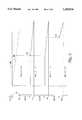
- FIG. 2is a timing diagram illustrating the effect of a DC voltage shift causing saturation of components of the line card of FIG. 1;
- FIG. 3is a block diagram of a continuous feedback DC cancelling network
- FIG. 4is a block diagram of a DC level shift control circuit for performing DC level control according to the present invention.
- FIG. 5is a timing diagram illustrating the operation of the DC level shift control circuit of FIG. 4.
- a block diagramis shown of a telephone line card 100 for interfacing an analog telephone 102 to a pulse code modulation (PCM) highway 104.
- the telephone 102includes a standard dial pad 105 with buttons for purposes of dialing as generally known.
- the telephone line card 100includes a SLIC 106 for performing a variety of functions, such as battery feed, overload protection, polarity reversal, on-hook transmission, switching regulation and current limiting.
- the telephone line card 100also includes a SLAC 108 for handling analog-to-digital. (A/D) and digital-to-analog (D/A) signal conversion, filtering, and interfacing with the pulse code modulation (PCM) highway 104.
- the SLAC 108also allows a user to program a desirable input impedance for the line card 100, as described below.
- the SLIC 106is connected to the telephone 102 via a two-wire connection, which includes two conductors for carrying "TIP” and "RING” signals, respectively, as known to those skilled in the art.
- the SLIC 106includes current mode amplifiers (not shown) for developing a current I L +I M through a series resistor R F on the TIP conductor and for developing a current I L -I M through another series resistor R F on the RING conductor as shown.
- the I L currentis the longitudinal or common mode current and I M is the metallic or differential current between the TIP and RING signals.
- I Lrepresents the DC current component and I M represents the AC current component for carrying the audio voice signals between the telephone 102 and the line card 100.
- a first differential amplifier 111 having a gain G TX1has its inputs connected across the resistor R HP1 and a second differential amplifier 113 having a gain G TX2 has its inputs connected across the resistor R HP2 .
- the G TX1 and G TX2 amplifiers 111, 113collectively detect the AC metallic voltage component measured across the R HP1 and R HP2 resistors, respectively, and preferably have gains of equal amplitude but opposite polarity for detecting the positive and negative portion of the AC component.
- the R HP1 , R HP2 resistorsare collectively referred to as a series resistor R HP , which is typically about 400-500 K ⁇ .
- the outputs of the G TX1 and G TX2 amplifiers 111, 113are summed together at a summing junction 110, for providing an analog audio voltage V TX at the four-wire output of the SLIC 106.
- the collective voltage across the series resistor R HPis referred to as the input signal V IN from the telephone 102, which is provided to the G TX amplifier 402 for developing the V TX signal, as shown in FIG. 4.
- the SLIC 106also includes a third amplifier 112 having its inputs connected across the capacitor C HP , which separates the DC component of the input signal to the SLIC 106. It is noted that the combination of the series resistor R HP , the capacitor C HP and the amplifier 112 function as a very low pass filter, which prevents the AC speech signals from entering the internal DC loop of the SLIC 106.
- the capacitor C HPsets the low frequency limit of the voice band response, where a typical value of 0.33 ⁇ F is used for optimizing voice band and DC loop performance. This low pass filter has a cutoff frequency of about 2 Hz or less.
- the output of the amplifier 112is connected to the non-inverting input terminal of another amplifier 114, which receives a reference voltage V REF at its inverting input terminal.
- the output of the amplifier 114is provided across a load impedance 116, where the amplifier 114 develops a current I L /K across the load 116.
- Kis a constant representing the internal current mode amplifier gain of the SLIC 106.
- the V REF signalis a bias voltage established by a longitudinal control loop for biasing the internal current mode SLIC amplifiers to operate in their linear region, i.e., for controlling the longitudinal line current to obtain an optimal common mode DC operating point for the current mode amplifiers.
- the output V TX of the adder 110is connected to the input of an A/D converter 118 within the SLAC 108.
- the A/D converter 118provides digital signals to a decimator 120. It is noted that the A/D converter 118 has a very high sampling rate, such as 4 megahertz (MHz), and preferably provides digital values having 6 bits, although other bit sizes are possible.
- the decimator 120reduces the sampling rate to approximately 8 kHz, and its output is provided to a transmitter path amplifier 121 having a gain GX, which is typically programmable within a range of 0-12 decibels (dB).
- the output of the GX amplifier 121is provided to the input of a filter block 122.
- the output of the filter block 122is provided to the input of a compression unit 124, which provides PCM codes to the transmit input of the PCM highway 104.
- the PCM highway 104provides PCM codes received from remote devices to an expansion unit 126 within the SLAC 108.
- the digital data provided from the expansion unit 126is provided to the input of a gain and filter block 128, which provides its output to an interpolator 130, which increases the sampling rate for conversion to analog.
- the output of the interpolator 130is provided to a D/A converter 132, which converts filtered and interpolated digital data into an analog output signal referred to as V RX , which is the receive signal of the analog four-wire interface between the SLIC 106 and the SLAC 108.
- the V RX signalis shown provided across an impedance 134 for developing a current I M /K into the receive summary node (RSN), not shown, of the SLIC 106 for controlling the metallic current of the two-wire interface.
- RSSNreceive summary node
- An impedance matching network 136is connected between the transmit and receive paths within the SLAC 108, where the impedance matching network 136 is typically connected to portions of the decimator 120 and the interpolator 130.
- the impedance matching network 136is programmable to allow a user to modify the effective termination impedance of the SLIC 106 to a desired value. This is generally used to match the two-wire impedance between the telephone 102 and the SLIC device 106 to allow maximum power transfer and minimize echoes during normal operation.
- the impedance matching network 136is insufficient to prevent saturation of electronic components due to sudden DC shifts caused by the DTMF generator 103.
- the keypad 105 on the telephone 102enables a user to dial a number, where the telephone 102 switches from the speaker/microphone to connect the DTMF generator 103 to assert corresponding dialing tones onto the TIP/RING two-wire interface.
- the DTMF generator 103has a different impedance than the speaker/microphone, where these impedances can differ by 50-200 ⁇ or more. Since the loop current may range from 25-45 mA, such switching results in a sudden DC level shift on the two-wire interface. The sudden DC voltage ranges from a few volts up to ten volts or more, thereby violating the maximum voltage range of the SLIC 106 and the SLAC 108, which operate in the range of 0-5 V.
- the series resistor R HP and the capacitor C HPhave a relatively large RC time constant, typically on the order of 100-150 ms, causing saturation of the G TX1 and G TX1 amplifiers 111, 113 (or the G TX amplifier 402), the A/D converter 118, the decimator 120 and the GX amplifier 121 for at least 80 ms or more.
- FIG. 2is a timing diagram illustrating the saturation situation of the telephone line card 100 operating without the benefit of the present invention.
- the output of the decimator 120is a digital value but is shown analog form as a voltage signal V S , which generally follows the V TX signal.
- the output of the GX amplifier 121is shown as a signal V GX1 .
- the curvesare plots of voltage versus time for the V IN , V TX , V S and V GX1 signals.
- the voltage levels for both the SLIC 106 and the SLAC 108are normalized, so that the saturation level for the internal components is 1 volt.
- the V IN signalis also normalized to a comparable voltage level relative to the normalized voltage levels of the telephone line card 100.
- All voltagesare initially zero at time T0.
- the userpresses a button on the keypad 105 and the DTMF 103 causes a 2 volt (2 V) DC voltage shift (normalized) of the V IN signal as shown in FIG. 2.
- 2 V2 volt
- the G TX amplifier 402almost immediately saturates to 1 V in response, as shown by the V TX signal.
- the voltage across the capacitor C HPbegins to decay as shown by curve 202. Although the voltage decay is exponential, it is shown as a linear decay for purposes of illustration since the time constant is relatively long.
- the G TX amplifier 402remains saturated and its voltage does not decay to one volt until at least 80 ms or more at a time T6.
- the gain GX of the amplifier 121is approximately 6 dB so that it effectively doubles its input voltage
- the GX amplifier 121is saturated even longer to a time T8, which is a at least 150 to 200 ms after time T2.
- This significantly large saturation periodresults in a "no detection” situation, since an interruption time of 20 ms or less is required for DTMF detection. This "no detection" situation is undesirable, since the DTMF is not detected by the line card 100 within the required specification of 20 ms or less, causing incorrect operation of the telephone system.
- a high pass filter networkcould be placed between the SLIC 106 and SLAC 108 to reject DC voltages and to prevent the SLAC 108 from saturating.
- the impedance of the line card 100would be altered by the high pass filter and it would be difficult to compensate for such an impedance change. This is true even using the impedance matching network 136 since it comprises a digital filter with a relatively high sampling rate, which therefore exhibits cycle limit problems.
- the high pass filterwould require relatively accurate components to sufficiently reduce variations from one line card to the next, where such variations would otherwise impact the two-wire interface return loss performance. Thus, expensive components would be required, such as a 5% or higher accuracy capacitor, which would impose a substantially expensive solution.
- a continuous DC voltage cancelling network 300is also contemplated, as shown in FIG. 3.
- an LPF 302 and a D/A converter 304are coupled in series between the filter block 122 and the input of the G TX amplifier 402.
- this solutionwould also substantially impact the two-wire return loss, especially in the low frequency band.
- the loop and system stabilitywould have to be monitored and compensated since a continuous feedback loop is implemented.
- Such continuous feedback loopsmay cause instability, oscillation and impedance matching problems that would have to be addressed.
- Such solutionsare possible though undesirable from design and cost standpoints.
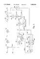
- FIG. 4a block diagram is shown of a DC level shift control circuit 400 according to the present invention as connected to components of the SLIC 106 and SLAC 108.
- the DC level shift control circuit 400filters out the DC components from the input audio signal, determines the gain setting in the transmit path using a duplicate gain amplifier, and introduces a DC adjust voltage which is opposite to the input DC level shift to avoid extended saturation.
- a summing junctionsubtracts the DC adjust voltage from the input voltage to counteract the DC shift.
- a long term filteris also included to correct for any DC residue caused by the DC level shift control circuit 400, as described below.
- An adder 401receives the V IN signal from the telephone line pair (not shown) on one of its two inputs, and subtracts a DC adjust feedback signal, referred to as V DCADJ , received at its other input from the V IN signal. This difference signal is provided to the G TX amplifier 402 for developing the V TX signal.
- the term "adder”generally refers to a summing junction for arithmetically combining two or more signals, such as through addition or subtraction.
- the adder 401may be implemented in any appropriate manner, such as using resistive summing junctions and a differential amplifier, etc.
- the other components of the SLIC 106 as shown in FIG. 1are not included in FIG. 4.
- a portion of the transmit path within the SLAC 108is repeated, including the A/D converter 118, the decimator 120 and the GX amplifier 121.
- the V S signal output of the decimator 120is connected to the input of a low pass filter (LPF) 404, having its output connected to the input of a digital switch 406.
- the switch 406is used to enable or disable DC level shift control according to the present invention, so that when the switch 406 is in the open state, the DC level shift control circuit 400 is disconnected and DC level control according to the present invention is not performed. It will be assumed, however, that the switch 406 is closed for enabling the DC level shift control circuit 400.
- the output of the LPF 404is coupled to the input of an amplifier 412 having the same gain GX as the GX amplifier 121.
- the GX amplifiers 121 and 412are both programmable and are programmed to always have the same gain.
- the output of the GX amplifier 412is provided to a threshold detection circuit TH1 414, which has a voltage threshold level preferably set to one-half the peak output voltage of the GX amplifier 412.
- the TH1 414asserts its binary output high, i.e., 5 V or logic 1, if the output voltage of the GX amplifier 412, referred to as a signal V GX2 , is greater than or equal to half of its positive peak voltage value, or less than or equal to half of its negative peak value but otherwise the TH1 414 asserts its output low, i.e., 0 V or logic 0.
- the peak voltages of V GX2is ⁇ 1 volt.
- the output of the LPF 404is also coupled to the input of a quantizer (QUAN) 408, which provides a quantized voltage signal at its output depending upon the voltage level at the output of the LPF (404).
- QUANquantizer
- the quantizer 408asserts a digital output value equivalent to +0.2 V if the output of the LPF 404 is greater than or equal to 0.2 V and outputs a digital value equivalent to -0.2 V if the output of the LPF 404 is less than or equal to -0.2 V. If the output of the LPF 404 is between -0.2 and +0.2 V, the output of the quantizer 408 is zero. In this manner, the resolution of the quantizer 408 is 0.2 V.
- the resolution of the quantizer 408is based upon the gain GX of the GX amplifier 121 when having a normalized maximum desired swing of 1 V, or 2 V peak to peak.
- a voltage of 0.2 Vis amplified by four to 0.8 V at an amplification of 12 dB, where 0.8 V is below the saturation point.
- the next 0.2 incrementcauses amplification above 1 volt, and thus into saturation.
- a higher gain rangewould require a finer quantizer resolution, which would mean a smaller voltage increment.
- a 0.2 V quantizer stepallows an inexpensive implementation.
- the quantizer resolutionmay be modified depending upon several factors, such as the maximum voltage swings of the SLIC and SLAC components and the maximum gain of the GX amplifiers 121, 412. Such variations are a matter of design choice.
- the output of the quantizer 408is connected to the input or source of a switch circuit 410, shown as a field effect transistor (FET). It is noted that a plurality of parallel FET switches are preferably incorporated for each bit, although a single FET is shown for clarity.
- the output of the TH1 414referred to as a binary signal ADJ, is provided to the control terminal or gate of the FET 410, where the TH1 414 turns the FET 410 either on or off depending upon the whether its threshold voltage level is exceeded or not.
- the drain of the FET 410is connected to one input of an adder junction 418 within an accumulator 416, where the adder 418 receives the output of a time delay 422 at its other input.
- the output of the adder 418is provided to the input of a D/A converter 424, and to one input terminal of a double pole, single throw switch device 420, which has its output terminal connected to the input of the time delay 422.
- the other input pole of the switch 420is connected to ground or logic zero. Again, a plurality of binary switches are used to implement the switch 420 although only one is shown.
- the time delay 422provides an output value equal to its input value after a predetermined time delay, which is preferably approximately 0.5 ms in the preferred embodiment.
- the switch 420is controlled by a binary signal RESET, where the switch 420 connects the output of the adder 418 to the input of the time delay 422 when the RESET signal is negated or low, but otherwise connects logic zero to the input of the time delay 422 when the RESET signal is asserted or high. In this manner, the RESET signal and the switch 420 are used to reset the accumulator 416 under certain conditions, as will be described in more detail below.
- the accumulator 416functions to sum an accumulated value with an incremental or quantized value from the quantizer 408 after the time delay determining the time delay 422, where the incremental value is preferably 0.2 V.
- the output of the adder 418either ramps up or down while the switches 410 and 420 are turned on, or stays at a steady DC value if the switch 410 is turned off.
- the accumulator 416outputs 0 V while the RESET signal is asserted.
- the digital voltage ramphas a relatively fast slope compared with the SLIC 106 since the time delay is chosen below 1 ms.
- the D/A converter 424converts the digital value from the adder 418 to an analog voltage.
- the output of the D/A converter 424provides the V DCADJ signal, which is subtracted from the V IN signal by the adder 401. In this manner, the V DCADJ signal offsets DC voltage shifts on the V IN signal as further described below.
- the output of the TH1 414is connected to an inverter 436, having its output connected to one input of a three-input AND logic gate 434.
- a long term DC level predictor and very narrow band filter (LLPF) 426receives the V S signal from the decimator 120 and has its output connected to one input of an adder 428.
- the output of the adder 418is provided to the other input of the adder 428, so that the output of the LLPF 426 is added to the output of the adder 418.
- the output value of the adder 428is provided to the input of a second threshold detection circuit TH2 430, which has its output connected to the input of an inverter 432.
- the output of the inverter 432is connected to a second input of the AND gate 434.
- the TH2 430asserts its output low if its input voltage is between -0.2 V and 0.2 V, but otherwise asserts its output high if the absolute value of its input voltage is greater than or equal to 0.2 V.
- the output of the adder 418is also connected to a third threshold detection circuit TH3 438, which is similar in its function to the TH2 430.
- the output of the TH3 438is connected to a third input of the AND gate 434.
- the AND gate 434asserts the RESET signal to reset the accumulator 416 under certain conditions, described below.
- the LPF 404has a cut-off frequency of approximately 40 Hz and a sampling rate of 8 kHz, where the LPF 404 has a transfer function as given by the following equation 1: ##EQU1## In this manner, the LPF 404 responds to a DC level shift of the audio signal in 4 ms or less.
- the LPF 404filters out desired voice frequencies (preferably between 200 Hz-3.4 kHz) and preserves the DC level, so that it determines if any sudden DC level shift has occurred on the input signal V IN .
- desired voice frequenciespreferably between 200 Hz-3.4 kHz
- transfer functions for the LPF 404can be utilized as is known to one of ordinary skill in the art, and still keeping within the teachings of the invention.
- the GX amplifier 412is provided to duplicated or otherwise represent the GX amplifier 121, where they both have the same gain GX. It is desired to monitor the DC level after the GX amplifier 121 to ensure proper operation of the DC level shift control circuit 400 according to the invention. For example, a 0.3 V DC shift sensed at the A/D converter 118 can cause the transmit path to almost saturate if the gain GX is set to 12 dB (decibels).
- the quantizer 408receives a continuous input level from the LPF 404 and outputs a quantized level.
- the FET 410is used to stop the accumulator 416 from ramping up or down.
- the FET 410is activated by the TH1 414 while the absolute value of the V GX1 signal is greater than or equal to 0.5 V.
- the ADJ signalpulls the gate and drain of the FET 410 low, thereby providing zero voltage to the adder 418.
- the accumulator 416provides a constant DC voltage. While the FET 410 is activated, the adder 418 adds the output of the quantizer 408 to the delayed output of the time delay 422, so that the adder 418 ramps up or down by the quantizer step level.
- the output signal of the adder 418is converted to the analog signal V DCADJ by the D/A converter 424 and subtracted from the V IN signal by the adder 401 to counteract DC voltage shifts.
- the voltage of the V DCADJ signalcauses the opposite problem in that it now represents an undesirable voltage shift in the opposite direction.
- the DC level shift control circuit 400corrects this in a similar manner, where this voltage is detected by the LPF 404 and amplified by the GX amplifier 412 causing the accumulator 416 to ramp back down to approximately zero.
- the LLPF 426has a 2 Hz cutoff frequency operates at a 250 Hz sampling frequency and has a transfer function according to the following equation 2: ##EQU2##
- the LLPF 426can have a different cutoff frequency, sampling frequency, and/or transfer function and still be within the scope of the invention as described herein.
- the LLPF 426is desired so that an instantaneous DC level shift, such as a narrow voltage spike, will not confuse the decision-making process of the DC level shift control circuit 400.
- the switch 420is needed to clear the DC residue (i.e., DC level ⁇ minimum threshold) during normal operation of the telephone line card 100. If the DC residue is not cleared during a normal telephone call, the dynamic range of the voice channel will be substantially reduced, which is an undesirable condition. In certain circumstances, for example, the output of the accumulator 416 may not go to zero but instead may supply a residue voltage equivalent to its voltage resolution of 0.2 V. This might occur when the V IN signal itself has a small DC offset less than this voltage resolution. This voltage residue would otherwise be amplified by the GX amplifier 121 in the transmit path and decrease the dynamic range of the audio signal.
- the LLPF 426is also used to detect this voltage residue and output a voltage equal to any DC residue generated by the accumulator 416 itself.
- the AND gate 434asserts the RESET signal to reset the accumulator 416 when the output of the GX amplifier 412 is within its threshold voltage, when the output of the accumulator 416 is not zero, and when the sum of the outputs of the adder 418 and the LLPF 426 is less than or equal to the resolution voltage of the accumulator 416.
- the threshold setting for the TH1 414should be set high enough so that an alternating input signal, such as a 200 Hz sinewave, does not trigger the DC level shift control circuit. However, setting the threshold too high may cause the transmit DC level to become very high, which is also undesirable. In that case, some of the signal may start to clip after being output from the GX amplifier 121. Therefore, a good choice of the threshold level for the first threshold detection circuit TH1 414 is approximately one-half of the saturation voltage of the GX amplifier 121 (and 412). Most of the voice signal with frequency greater than 100 Hz has already been partially filtered by the LPF 404, so that the TH1 414 primarily receives a DC signal.
- the feedback concept according to the preferred embodimentis not continuous, but rather utilizes a quantized, discontinuous filter block. Therefore, the stability problems associated with conventional methods for handling DC level shifts are not present in the system according to the invention.
- FIG. 5a timing diagram is shown to illustrate operation of the DC level shift control circuit 400 according to the present invention.
- the V IN signal, the V TX signal, the V S signal, the V GX1 signal, the output of the LPF 404 (shown as LPF), the V GX2 signal, the ADJ signal, the V DCADJ signal, the output of the LLPF 426 (shown as LLPF) and the RESET signal as output by the AND gate 434are shown plotted versus time. For clarity, any voice signals are ignored, so that only the response to a DC step voltage is shown.
- the worst caseis illustrated, where an input of 2 V is asserted on the V IN signal and remains asserted for a period of time, where it is understood that an actual DC voltage shift caused by the DTMF generator 103 would decay over time. Also, the DC step voltage asserted on the V IN signal will also be suddenly removed to illustrate response of the DC level shift control circuit 400 in response to a worst case scenario.
- V INV IN signal
- a 2 V DC step voltageis applied at time T2 on the V IN signal, which immediately saturates the G TX amplifier 402, the A/D converter 118, the decimator 120, the GX amplifier 121, the LPF 404 and the GX amplifier 412, so that the V TX , V S , V GX1 , LPF and V GX2 signals rise to 1 V.
- the ADJ signalis asserted high, turning on the FET 410 so that the quantizer 408 provides +0.2 V to the accumulator 416.
- the accumulator 416responds almost immediately or within less than 1 ms at a time T4 and begins ramping up at 0.2 V increments, where each step is about 0.5 ms caused by the time delay 422.
- the V DCADJ signalreaches 1 V so that the overvoltage of the V IN signal is cancelled out by the adder 401.
- the G TX amplifier 402, the A/D converter 118 and the decimator 120leave the saturation region.
- the accumulator 416drives the V DCADJ signal above 1 V so that the V TX signal begins ramping down by 0.2 V increments.
- the GX amplifier 121Since the GX amplifier 121 has a gain of 6 dB and thus doubles its input voltage, it responds more slowly, but then quickly ramps down beginning at time T10.
- the LPF 404responds fairly quickly to the output of the decimator 120 and begins ramping down at approximately time T8.
- the GX amplifier 412also having a gain of 6 dB ramps down in response to the output of the LPF 404 until going to approximately 0.4 V at time T12.
- the accumulator 416has ramped up to approximately 1.8 V, which is a 0.2 V differential with respect to the 2 V DC step signal asserted on the V IN signal.
- the 0.2 Vis amplified to 0.4 V by the GX amplifier 412, which is below the threshold of the TH1 414 at time T12. Therefore, the ADJ signal goes low at approximately time T12, shutting off the FET 410 so that the accumulator 416 maintains the V DCADJ signal at approximately 1.8 V.
- the V DCADJ signalremains at 1.8 V to offset the 2 V step voltage asserted on the V IN signal.
- the LLPF 426responds much more slowly than the LPF 404 and thus climbs towards 0.2 V after the V S signal drops to 0.2 V.
- the G TX amplifier 402the A/D converter 118, the decimator 120, the GX amplifier 121, the LPF 404 and the GX amplifier 412 all saturate at -1 V at approximately time T20.
- the ADJ signalis asserted high in response to the GX amplifier 412 reaching its negative saturation point, thereby activating the FET 410 at time T20.
- the quantizer 408provides a voltage of -0.2 V to the accumulator 416, which begins stepping downwards, thereby reducing the voltage of the V DCADJ signal beginning at time T22.
- the accumulator 416steps down in approximately 0.2 V steps, each occurring within approximately 0.5 ms.
- the V DCADJ signaleventually reaches one volt at time T24 and then drops below one volt 0.5 ms later at time T26, at which time the V TX and the output of the decimator 120 begin responding by rising above the -1 V saturation point.
- the LPF 404begins ramping up at about time T26.
- the GX amplifiers 121, 412respond more slowly at time T28, but eventually rise to -0.4 V at time T30, which is below the threshold level of the TH1 414.
- the TH1 414asserts the ADJ signal low, thereby turning off the FET 410, so that the output of the accumulator 416 remains at 0.2 V.
- the V DCADJ signalremains at 0.2 V.
- the V TX , V S and LPF signalsremain at -0.2 V and the V GX1 and V GX2 signals remain at -0.4 V at time T30.
- the LLPF 426has not yet reached 0.2 V at time T20.
- the LLPF 426responds, albeit slowly, to the sudden drop of the V S signal at time T20 and begins to fall until eventually reaching 0 V at about time T32.
- the DC level shift control circuit 400responds within 4 to 5 ms of a DC step voltage applied on the V IN signal pulling the primary components including the GX amplifier 121 out of saturation within 5 ms.
- the line card 100is capable of detecting the DTMF generator 103.
- the input step voltage or shift signaldecays over time and the DC level shift control circuit 400 responds accordingly by reducing the V DCADJ signal back down to near zero or within 0.2 V.
- the output of the accumulator 416has not decreased all the way to zero, but instead supplies a residue voltage such that the V DCADJ signal is at 0.2 V after the adjustment function is complete.
- This voltage residueis subtracted from V IN and then eventually multiplied by the GX amplifier 121 to -0.4 V if its gain is 6 dB, where this residual adjust voltage decreases the dynamic range of audio voice signals on the transmit path.
- the reset logic of the AND gate 434prevents this undesirable situation.
- the absolute value of the output of the adder junction 418is greater than or equal to 0.2 V
- the TH3 438asserts its output high for a first reset condition.
- the inverter 436asserts its output high meeting a second reset condition.
- the output of the LLPF 426 detecting residual DC adjust voltageis added to the output of the adder 418, and the absolute value of the difference is less than 0.2 V, the TH2 430 asserts its output low and the inverter 432 asserts its output high meeting the third and final reset condition, so that the AND gate 434 asserts the RESET signal high at about time T32.
- the switch 420is switched to provide all zeros, and all zeros are provided from the FET 410, so that the output of the accumulator 416 is now at 0 V at a time T34, thereby resetting the DC level shift control circuit 400 according to the present invention.
- the V GX1 signalis reset to 0 V at time T34, removing the voltage residue.
- the RESET signalgoes low at about time T36. It is noted that the RESET pulse typically occurs much faster, but its width is emphasized for purposes of clarity.
- DC level controlallows the SLIC and SLAC devices of a telephone line card to operate normally even in situations involving a sudden DC jump caused by a DTMF generator impedance change.
- the invention as described hereinkeeps the devices of an electronic line card from saturating for significant periods of time, thereby allowing DTMF detection.
- the present inventionprovides a quantized and discontinuous solution so that the AC functions remain substantially unaffected, even at the very low frequency range. Thus, impedance matching and stability problems are avoided.
- the components used to implement the present inventionmay be common, off the shelf and inexpensive components, resulting in a cost-effective solution.
Landscapes
- Engineering & Computer Science (AREA)
- Signal Processing (AREA)
- Power Engineering (AREA)
- Interface Circuits In Exchanges (AREA)
- Analogue/Digital Conversion (AREA)
Abstract
Description
Claims (24)
Priority Applications (4)
| Application Number | Priority Date | Filing Date | Title |
|---|---|---|---|
| US08/398,295US5583934A (en) | 1995-03-03 | 1995-03-03 | DC level control for an electronic telephone line card |
| PCT/US1996/002835WO1996027970A1 (en) | 1995-03-03 | 1996-03-01 | Dc level control for an electronic telephone line card |
| EP96908607AEP0792548B1 (en) | 1995-03-03 | 1996-03-01 | Dc level control for an electronic telephone line card |
| DE69633605TDE69633605T2 (en) | 1995-03-03 | 1996-03-01 | DC POWER CONTROL FOR ELECTRONIC REMOTE CONTROL CARD |
Applications Claiming Priority (1)
| Application Number | Priority Date | Filing Date | Title |
|---|---|---|---|
| US08/398,295US5583934A (en) | 1995-03-03 | 1995-03-03 | DC level control for an electronic telephone line card |
Publications (1)
| Publication Number | Publication Date |
|---|---|
| US5583934Atrue US5583934A (en) | 1996-12-10 |
Family
ID=23574832
Family Applications (1)
| Application Number | Title | Priority Date | Filing Date |
|---|---|---|---|
| US08/398,295Expired - LifetimeUS5583934A (en) | 1995-03-03 | 1995-03-03 | DC level control for an electronic telephone line card |
Country Status (4)
| Country | Link |
|---|---|
| US (1) | US5583934A (en) |
| EP (1) | EP0792548B1 (en) |
| DE (1) | DE69633605T2 (en) |
| WO (1) | WO1996027970A1 (en) |
Cited By (35)
| Publication number | Priority date | Publication date | Assignee | Title |
|---|---|---|---|---|
| WO1999034581A1 (en)* | 1997-12-30 | 1999-07-08 | Alcatel Usa Sourcing, L.P. | Telecommunications terminal card |
| US5926544A (en)* | 1997-06-06 | 1999-07-20 | Advanced Micro Devices, Inc. | Direct current feed with line status change adaptation in a communication system |
| EP1011250A1 (en)* | 1998-12-18 | 2000-06-21 | Lucent Technologies Inc. | A system and method for allocating overhead voltage in the transmission of pots and xdsl signals |
| US6178241B1 (en)* | 1997-06-06 | 2001-01-23 | Legerity, Inc. | Switch hook status determination in a communication system |
| US6219417B1 (en)* | 1997-06-06 | 2001-04-17 | Advanced Micro Devices, Inc. | Ring trip detection in a communication system |
| WO2001030062A1 (en)* | 1999-10-20 | 2001-04-26 | Legerity, Inc. | Method and apparatus for dc feed control |
| US20020118819A1 (en)* | 2000-12-29 | 2002-08-29 | Jin Li | Method and apparatus for detecting line card threshold |
| US20030059062A1 (en)* | 2001-09-24 | 2003-03-27 | Soo Kee Eng | Circuit to prevent acoustic feedback for a cellular speakerphone |
| US6560323B2 (en) | 1994-04-19 | 2003-05-06 | T-Netix, Inc. | Computer-based method and apparatus for controlling, monitoring, recording and reporting telephone access |
| US6611583B1 (en)* | 1994-04-19 | 2003-08-26 | T-Netix, Inc. | Computer-based method and apparatus for controlling, monitoring, recording and reporting telephone access |
| US20030202653A1 (en)* | 2002-04-30 | 2003-10-30 | Chan Wing K. | Generic line impedance matching circuit using decomposed configurable transfer functions |
| US6665380B1 (en) | 1999-01-11 | 2003-12-16 | T-Netix, Inc. | Inmate messaging system and method |
| US6668045B1 (en) | 2000-10-30 | 2003-12-23 | T-Netix, Inc. | Message screening, delivery and billing system |
| US20040120507A1 (en)* | 2002-12-18 | 2004-06-24 | Nasser Pooladian | Ring signal voltage offset for subscriber line interface circuit |
| US6763099B1 (en) | 1999-11-05 | 2004-07-13 | T-Netix, Inc. | Advanced three way call detection system and method using spread spectrum techniques |
| US6865269B1 (en)* | 2000-04-26 | 2005-03-08 | Legerity, Inc. | Method and apparatus for switch hook detection |
| US6920209B1 (en) | 1994-04-19 | 2005-07-19 | T-Netix, Inc. | Computer-based method and apparatus for controlling, monitoring, recording and reporting telephone access |
| US7248680B1 (en) | 1994-04-19 | 2007-07-24 | T-Netix, Inc. | Computer-based method and apparatus for controlling, monitoring, recording and reporting telephone access |
| US7317793B2 (en) | 2003-01-30 | 2008-01-08 | Serconet Ltd | Method and system for providing DC power on local telephone lines |
| US20080159367A1 (en)* | 2005-06-21 | 2008-07-03 | Nec Corporation | Signal Processing Device and Method |
| US7424031B2 (en) | 1998-07-28 | 2008-09-09 | Serconet, Ltd. | Local area network of serial intelligent cells |
| DE102007021738B3 (en)* | 2007-05-09 | 2008-12-24 | Infineon Technologies Ag | Method for recovering information signal from input signal, particularly for use in data communication devices, involves generating direct current voltage by subtracting low-pass-filtered control voltage from reference voltage |
| US7483524B2 (en) | 1999-07-20 | 2009-01-27 | Serconet, Ltd | Network for telephony and data communication |
| US7505406B1 (en) | 2001-07-13 | 2009-03-17 | Evercom Systems, Inc. | Public telephone control with voice over internet protocol transmission |
| US7522714B2 (en) | 2000-03-20 | 2009-04-21 | Serconet Ltd. | Telephone outlet for implementing a local area network over telephone lines and a local area network using such outlets |
| US7529357B1 (en) | 2003-08-15 | 2009-05-05 | Evercom Systems, Inc. | Inmate management and call processing systems and methods |
| US7899167B1 (en) | 2003-08-15 | 2011-03-01 | Securus Technologies, Inc. | Centralized call processing |
| US7916845B2 (en) | 2006-04-13 | 2011-03-29 | Securus Technologies, Inc. | Unauthorized call activity detection and prevention systems and methods for a Voice over Internet Protocol environment |
| US8000269B1 (en) | 2001-07-13 | 2011-08-16 | Securus Technologies, Inc. | Call processing with voice over internet protocol transmission |
| US8582598B2 (en) | 1999-07-07 | 2013-11-12 | Mosaid Technologies Incorporated | Local area network for distributing data communication, sensing and control signals |
| US9560193B1 (en) | 2002-04-29 | 2017-01-31 | Securus Technologies, Inc. | Systems and methods for detecting a call anomaly using biometric identification |
| US9990683B2 (en) | 2002-04-29 | 2018-06-05 | Securus Technologies, Inc. | Systems and methods for acquiring, accessing, and analyzing investigative information |
| US10115080B2 (en) | 2002-04-29 | 2018-10-30 | Securus Technologies, Inc. | System and method for proactively establishing a third-party payment account for services rendered to a resident of a controlled-environment facility |
| US10796392B1 (en) | 2007-05-22 | 2020-10-06 | Securus Technologies, Llc | Systems and methods for facilitating booking, bonding and release |
| US10986164B2 (en) | 2004-01-13 | 2021-04-20 | May Patents Ltd. | Information device |
Families Citing this family (2)
| Publication number | Priority date | Publication date | Assignee | Title |
|---|---|---|---|---|
| JP2994630B2 (en) | 1997-12-10 | 1999-12-27 | 松下電器産業株式会社 | Display device capable of adjusting the number of subfields by brightness |
| DE19802826C2 (en)* | 1998-01-26 | 1999-11-18 | Siemens Ag | Method for comparing current values of a subscriber set falsified by disturbance variables |
Citations (6)
| Publication number | Priority date | Publication date | Assignee | Title |
|---|---|---|---|---|
| US4065726A (en)* | 1976-08-11 | 1977-12-27 | The United States Of America As Represented By The Secretary Of The Navy | Negative feedback amplifier and lever shifter |
| US4410876A (en)* | 1976-09-27 | 1983-10-18 | Sony Corporation | D.C. Stabilized analog-to-digital converter |
| US4602374A (en)* | 1984-02-27 | 1986-07-22 | Nippon Telegraph & Telephone Public Corporation | Multi-level decision circuit |
| US4766417A (en)* | 1986-06-07 | 1988-08-23 | Sony Corporation | Automatic offset compensating bipolar A/D converter circuit |
| US4860010A (en)* | 1986-06-27 | 1989-08-22 | Fujitsu Limited | Automatic drift control circuit |
| US5027389A (en)* | 1988-08-29 | 1991-06-25 | Industrial Technology Research Institute | Self-compensated dual tone multiple frequency generator |
Family Cites Families (1)
| Publication number | Priority date | Publication date | Assignee | Title |
|---|---|---|---|---|
| SE457923B (en)* | 1987-06-15 | 1989-02-06 | Ellemtel Utvecklings Ab | DEVICE TO ACHIEVE A CONTROLLABLE LINE CUT IMPEDANCE |
- 1995
- 1995-03-03USUS08/398,295patent/US5583934A/ennot_activeExpired - Lifetime
- 1996
- 1996-03-01WOPCT/US1996/002835patent/WO1996027970A1/enactiveIP Right Grant
- 1996-03-01EPEP96908607Apatent/EP0792548B1/ennot_activeExpired - Lifetime
- 1996-03-01DEDE69633605Tpatent/DE69633605T2/ennot_activeExpired - Lifetime
Patent Citations (6)
| Publication number | Priority date | Publication date | Assignee | Title |
|---|---|---|---|---|
| US4065726A (en)* | 1976-08-11 | 1977-12-27 | The United States Of America As Represented By The Secretary Of The Navy | Negative feedback amplifier and lever shifter |
| US4410876A (en)* | 1976-09-27 | 1983-10-18 | Sony Corporation | D.C. Stabilized analog-to-digital converter |
| US4602374A (en)* | 1984-02-27 | 1986-07-22 | Nippon Telegraph & Telephone Public Corporation | Multi-level decision circuit |
| US4766417A (en)* | 1986-06-07 | 1988-08-23 | Sony Corporation | Automatic offset compensating bipolar A/D converter circuit |
| US4860010A (en)* | 1986-06-27 | 1989-08-22 | Fujitsu Limited | Automatic drift control circuit |
| US5027389A (en)* | 1988-08-29 | 1991-06-25 | Industrial Technology Research Institute | Self-compensated dual tone multiple frequency generator |
Cited By (73)
| Publication number | Priority date | Publication date | Assignee | Title |
|---|---|---|---|---|
| US6920209B1 (en) | 1994-04-19 | 2005-07-19 | T-Netix, Inc. | Computer-based method and apparatus for controlling, monitoring, recording and reporting telephone access |
| US7889847B2 (en) | 1994-04-19 | 2011-02-15 | Securus Technologies Holdings, Inc. | Computer-based method and apparatus for controlling, monitoring, recording and reporting telephone access |
| US7248680B1 (en) | 1994-04-19 | 2007-07-24 | T-Netix, Inc. | Computer-based method and apparatus for controlling, monitoring, recording and reporting telephone access |
| US20070041545A1 (en)* | 1994-04-19 | 2007-02-22 | Gainsboro Jay L | Computer-based method and apparatus for controlling, monitoring, recording and reporting telephone access |
| US7106843B1 (en) | 1994-04-19 | 2006-09-12 | T-Netix, Inc. | Computer-based method and apparatus for controlling, monitoring, recording and reporting telephone access |
| US6560323B2 (en) | 1994-04-19 | 2003-05-06 | T-Netix, Inc. | Computer-based method and apparatus for controlling, monitoring, recording and reporting telephone access |
| US6611583B1 (en)* | 1994-04-19 | 2003-08-26 | T-Netix, Inc. | Computer-based method and apparatus for controlling, monitoring, recording and reporting telephone access |
| US5926544A (en)* | 1997-06-06 | 1999-07-20 | Advanced Micro Devices, Inc. | Direct current feed with line status change adaptation in a communication system |
| US6178241B1 (en)* | 1997-06-06 | 2001-01-23 | Legerity, Inc. | Switch hook status determination in a communication system |
| US6219417B1 (en)* | 1997-06-06 | 2001-04-17 | Advanced Micro Devices, Inc. | Ring trip detection in a communication system |
| US6396922B1 (en) | 1997-12-30 | 2002-05-28 | Alcatel Usa Sourcing, L.P. | Telecommunications terminal card |
| WO1999034581A1 (en)* | 1997-12-30 | 1999-07-08 | Alcatel Usa Sourcing, L.P. | Telecommunications terminal card |
| US7986708B2 (en) | 1998-07-28 | 2011-07-26 | Mosaid Technologies Incorporated | Local area network of serial intelligent cells |
| US7969917B2 (en) | 1998-07-28 | 2011-06-28 | Mosaid Technologies Incorporated | Local area network of serial intelligent cells |
| US7852874B2 (en) | 1998-07-28 | 2010-12-14 | Mosaid Technologies Incorporated | Local area network of serial intelligent cells |
| US7978726B2 (en) | 1998-07-28 | 2011-07-12 | Mosaid Technologies Incorporated | Local area network of serial intelligent cells |
| US8867523B2 (en) | 1998-07-28 | 2014-10-21 | Conversant Intellectual Property Management Incorporated | Local area network of serial intelligent cells |
| US7653015B2 (en) | 1998-07-28 | 2010-01-26 | Mosaid Technologies Incorporated | Local area network of serial intelligent cells |
| US7424031B2 (en) | 1998-07-28 | 2008-09-09 | Serconet, Ltd. | Local area network of serial intelligent cells |
| US7830858B2 (en) | 1998-07-28 | 2010-11-09 | Mosaid Technologies Incorporated | Local area network of serial intelligent cells |
| US8885660B2 (en) | 1998-07-28 | 2014-11-11 | Conversant Intellectual Property Management Incorporated | Local area network of serial intelligent cells |
| US8270430B2 (en) | 1998-07-28 | 2012-09-18 | Mosaid Technologies Incorporated | Local area network of serial intelligent cells |
| US8908673B2 (en) | 1998-07-28 | 2014-12-09 | Conversant Intellectual Property Management Incorporated | Local area network of serial intelligent cells |
| US7965735B2 (en) | 1998-07-28 | 2011-06-21 | Mosaid Technologies Incorporated | Local area network of serial intelligent cells |
| US8325636B2 (en) | 1998-07-28 | 2012-12-04 | Mosaid Technologies Incorporated | Local area network of serial intelligent cells |
| US8885659B2 (en) | 1998-07-28 | 2014-11-11 | Conversant Intellectual Property Management Incorporated | Local area network of serial intelligent cells |
| EP1011250A1 (en)* | 1998-12-18 | 2000-06-21 | Lucent Technologies Inc. | A system and method for allocating overhead voltage in the transmission of pots and xdsl signals |
| US6748078B1 (en) | 1998-12-18 | 2004-06-08 | Lucent Technologies Inc. | System and method for allocating overhead voltage in the transmission of pots and XDSL signals |
| US6665380B1 (en) | 1999-01-11 | 2003-12-16 | T-Netix, Inc. | Inmate messaging system and method |
| US8582598B2 (en) | 1999-07-07 | 2013-11-12 | Mosaid Technologies Incorporated | Local area network for distributing data communication, sensing and control signals |
| US7492875B2 (en) | 1999-07-20 | 2009-02-17 | Serconet, Ltd. | Network for telephony and data communication |
| US7483524B2 (en) | 1999-07-20 | 2009-01-27 | Serconet, Ltd | Network for telephony and data communication |
| US8929523B2 (en) | 1999-07-20 | 2015-01-06 | Conversant Intellectual Property Management Inc. | Network for telephony and data communication |
| US7522713B2 (en) | 1999-07-20 | 2009-04-21 | Serconet, Ltd. | Network for telephony and data communication |
| US8351582B2 (en) | 1999-07-20 | 2013-01-08 | Mosaid Technologies Incorporated | Network for telephony and data communication |
| WO2001030062A1 (en)* | 1999-10-20 | 2001-04-26 | Legerity, Inc. | Method and apparatus for dc feed control |
| US6671373B1 (en) | 1999-10-20 | 2003-12-30 | Legerity, Inc. | Method and apparatus for DC feed control |
| US6763099B1 (en) | 1999-11-05 | 2004-07-13 | T-Netix, Inc. | Advanced three way call detection system and method using spread spectrum techniques |
| US8363797B2 (en) | 2000-03-20 | 2013-01-29 | Mosaid Technologies Incorporated | Telephone outlet for implementing a local area network over telephone lines and a local area network using such outlets |
| US8855277B2 (en) | 2000-03-20 | 2014-10-07 | Conversant Intellectual Property Managment Incorporated | Telephone outlet for implementing a local area network over telephone lines and a local area network using such outlets |
| US7522714B2 (en) | 2000-03-20 | 2009-04-21 | Serconet Ltd. | Telephone outlet for implementing a local area network over telephone lines and a local area network using such outlets |
| US7715534B2 (en) | 2000-03-20 | 2010-05-11 | Mosaid Technologies Incorporated | Telephone outlet for implementing a local area network over telephone lines and a local area network using such outlets |
| US6865269B1 (en)* | 2000-04-26 | 2005-03-08 | Legerity, Inc. | Method and apparatus for switch hook detection |
| US6668045B1 (en) | 2000-10-30 | 2003-12-23 | T-Netix, Inc. | Message screening, delivery and billing system |
| US20020118819A1 (en)* | 2000-12-29 | 2002-08-29 | Jin Li | Method and apparatus for detecting line card threshold |
| US7239695B2 (en)* | 2000-12-29 | 2007-07-03 | Legerity, Inc. | Method and apparatus for detecting line card threshold |
| US8000269B1 (en) | 2001-07-13 | 2011-08-16 | Securus Technologies, Inc. | Call processing with voice over internet protocol transmission |
| US7505406B1 (en) | 2001-07-13 | 2009-03-17 | Evercom Systems, Inc. | Public telephone control with voice over internet protocol transmission |
| US7027604B2 (en) | 2001-09-24 | 2006-04-11 | Motorola, Inc. | Circuit to prevent acoustic feedback for a cellular speakerphone |
| US20030059062A1 (en)* | 2001-09-24 | 2003-03-27 | Soo Kee Eng | Circuit to prevent acoustic feedback for a cellular speakerphone |
| US10178224B2 (en) | 2002-04-29 | 2019-01-08 | Securus Technologies, Inc. | Systems and methods for detecting a call anomaly using biometric identification |
| US10115080B2 (en) | 2002-04-29 | 2018-10-30 | Securus Technologies, Inc. | System and method for proactively establishing a third-party payment account for services rendered to a resident of a controlled-environment facility |
| US9990683B2 (en) | 2002-04-29 | 2018-06-05 | Securus Technologies, Inc. | Systems and methods for acquiring, accessing, and analyzing investigative information |
| US9560193B1 (en) | 2002-04-29 | 2017-01-31 | Securus Technologies, Inc. | Systems and methods for detecting a call anomaly using biometric identification |
| US20030202653A1 (en)* | 2002-04-30 | 2003-10-30 | Chan Wing K. | Generic line impedance matching circuit using decomposed configurable transfer functions |
| US7062037B2 (en)* | 2002-04-30 | 2006-06-13 | Texas Instruments Incorporated | Generic line impedance matching circuit using decomposed configurable transfer functions |
| US20040120507A1 (en)* | 2002-12-18 | 2004-06-24 | Nasser Pooladian | Ring signal voltage offset for subscriber line interface circuit |
| US7702095B2 (en) | 2003-01-30 | 2010-04-20 | Mosaid Technologies Incorporated | Method and system for providing DC power on local telephone lines |
| US7317793B2 (en) | 2003-01-30 | 2008-01-08 | Serconet Ltd | Method and system for providing DC power on local telephone lines |
| US8787562B2 (en) | 2003-01-30 | 2014-07-22 | Conversant Intellectual Property Management Inc. | Method and system for providing DC power on local telephone lines |
| US8107618B2 (en) | 2003-01-30 | 2012-01-31 | Mosaid Technologies Incorporated | Method and system for providing DC power on local telephone lines |
| US8340260B1 (en) | 2003-08-15 | 2012-12-25 | Securus Technologies, Inc. | Inmate management and call processing systems and methods |
| US7899167B1 (en) | 2003-08-15 | 2011-03-01 | Securus Technologies, Inc. | Centralized call processing |
| US7529357B1 (en) | 2003-08-15 | 2009-05-05 | Evercom Systems, Inc. | Inmate management and call processing systems and methods |
| US10740861B1 (en) | 2003-11-24 | 2020-08-11 | Securus Technologies, Inc. | Systems and methods for acquiring, accessing, and analyzing investigative information |
| US10986164B2 (en) | 2004-01-13 | 2021-04-20 | May Patents Ltd. | Information device |
| US11032353B2 (en) | 2004-01-13 | 2021-06-08 | May Patents Ltd. | Information device |
| US11095708B2 (en) | 2004-01-13 | 2021-08-17 | May Patents Ltd. | Information device |
| US20080159367A1 (en)* | 2005-06-21 | 2008-07-03 | Nec Corporation | Signal Processing Device and Method |
| US8059757B2 (en)* | 2005-06-21 | 2011-11-15 | Nec Corporation | Signal processing device and method |
| US7916845B2 (en) | 2006-04-13 | 2011-03-29 | Securus Technologies, Inc. | Unauthorized call activity detection and prevention systems and methods for a Voice over Internet Protocol environment |
| DE102007021738B3 (en)* | 2007-05-09 | 2008-12-24 | Infineon Technologies Ag | Method for recovering information signal from input signal, particularly for use in data communication devices, involves generating direct current voltage by subtracting low-pass-filtered control voltage from reference voltage |
| US10796392B1 (en) | 2007-05-22 | 2020-10-06 | Securus Technologies, Llc | Systems and methods for facilitating booking, bonding and release |
Also Published As
| Publication number | Publication date |
|---|---|
| DE69633605T2 (en) | 2006-03-02 |
| EP0792548A1 (en) | 1997-09-03 |
| WO1996027970A1 (en) | 1996-09-12 |
| EP0792548B1 (en) | 2004-10-13 |
| DE69633605D1 (en) | 2004-11-18 |
Similar Documents
| Publication | Publication Date | Title |
|---|---|---|
| US5583934A (en) | DC level control for an electronic telephone line card | |
| US7190784B2 (en) | Method and apparatus for adaptive DC level control | |
| US5353348A (en) | Double echo cancelling system | |
| US5369711A (en) | Automatic gain control for a headset | |
| US4555596A (en) | Loudspeaking telephones | |
| US5533119A (en) | Method and apparatus for sidetone optimization | |
| US5893034A (en) | Cordless parent/slave telephone set with improved sidetone handling | |
| KR100446585B1 (en) | A method and system for scaleable near-end speech cancellation for tip and ring tone signal detectors | |
| US4580013A (en) | Handsfree communication apparatus and method | |
| EP0272068B1 (en) | Microphone circuit | |
| WO1993021722A1 (en) | Wideband telephone line interface circuit | |
| EP0495672B1 (en) | White noise suppression circuit | |
| US3691311A (en) | Telephone user set | |
| US7239695B2 (en) | Method and apparatus for detecting line card threshold | |
| FR2532134A1 (en) | SPEAKER TELEPHONE DEVICE | |
| KR100357801B1 (en) | Lateral sound reduction circuit in receive signal path | |
| KR940002146B1 (en) | Telephone system | |
| EP0361884B1 (en) | Noise reduction in speech transmitter circuits | |
| US6930751B2 (en) | Method and apparatus for reducing false hook detection | |
| JPH0445323Y2 (en) | ||
| KR910003391B1 (en) | Half Duplex Voice Transceiver | |
| JP2789997B2 (en) | Telephone equipment | |
| US6865269B1 (en) | Method and apparatus for switch hook detection | |
| KR200306837Y1 (en) | Call volume control device of WLL terminal | |
| KR100207819B1 (en) | Telephone for inaudibles |
Legal Events
| Date | Code | Title | Description |
|---|---|---|---|
| AS | Assignment | Owner name:ADVANCED MICRO DEVICES, INC., CALIFORNIA Free format text:ASSIGNMENT OF ASSIGNORS INTEREST;ASSIGNOR:ZHOU, YAN;REEL/FRAME:007382/0920 Effective date:19950301 | |
| STCF | Information on status: patent grant | Free format text:PATENTED CASE | |
| FPAY | Fee payment | Year of fee payment:4 | |
| AS | Assignment | Owner name:MORGAN STANLEY & CO. INCORPORATED, NEW YORK Free format text:SECURITY INTEREST;ASSIGNOR:LEGERITY, INC.;REEL/FRAME:011601/0539 Effective date:20000804 | |
| AS | Assignment | Owner name:LEGERITY, INC., TEXAS Free format text:ASSIGNMENT OF ASSIGNORS INTEREST;ASSIGNOR:ADVANCED MICRO DEVICES, INC.;REEL/FRAME:011700/0686 Effective date:20000731 | |
| AS | Assignment | Owner name:MORGAN STANLEY & CO. INCORPORATED, AS FACILITY COL Free format text:SECURITY AGREEMENT;ASSIGNORS:LEGERITY, INC.;LEGERITY HOLDINGS, INC.;LEGERITY INTERNATIONAL, INC.;REEL/FRAME:013372/0063 Effective date:20020930 | |
| FPAY | Fee payment | Year of fee payment:8 | |
| AS | Assignment | Owner name:LEGERITY, INC., TEXAS Free format text:RELEASE BY SECURED PARTY;ASSIGNOR:MORGAN STANLEY SENIOR FUNDING INC;REEL/FRAME:019640/0676 Effective date:20070803 Owner name:LEGERITY, INC.,TEXAS Free format text:RELEASE BY SECURED PARTY;ASSIGNOR:MORGAN STANLEY SENIOR FUNDING INC;REEL/FRAME:019640/0676 Effective date:20070803 | |
| FPAY | Fee payment | Year of fee payment:12 | |
| AS | Assignment | Owner name:MICROSEMI SEMICONDUCTOR (U.S.) INC., TEXAS Free format text:CHANGE OF NAME;ASSIGNOR:ZARLINK SEMICONDUCTOR (U.S.) INC.;REEL/FRAME:031746/0214 Effective date:20111121 Owner name:ZARLINK SEMICONDUCTOR (U.S.) INC., TEXAS Free format text:MERGER;ASSIGNOR:LEGERITY, INC.;REEL/FRAME:031746/0171 Effective date:20071130 | |
| AS | Assignment | Owner name:MORGAN STANLEY & CO. LLC, NEW YORK Free format text:PATENT SECURITY AGREEMENT;ASSIGNOR:MICROSEMI SEMICONDUCTOR (U.S.) INC.;REEL/FRAME:031729/0667 Effective date:20131125 | |
| AS | Assignment | Owner name:BANK OF AMERICA, N.A., AS SUCCESSOR AGENT, NORTH C Free format text:NOTICE OF SUCCESSION OF AGENCY;ASSIGNOR:ROYAL BANK OF CANADA (AS SUCCESSOR TO MORGAN STANLEY & CO. LLC);REEL/FRAME:035657/0223 Effective date:20150402 | |
| AS | Assignment | Owner name:MICROSEMI SOC CORP., A CALIFORNIA CORPORATION, CAL Free format text:RELEASE BY SECURED PARTY;ASSIGNOR:BANK OF AMERICA, N.A.;REEL/FRAME:037558/0711 Effective date:20160115 Owner name:MICROSEMI COMMUNICATIONS, INC. (F/K/A VITESSE SEMI Free format text:RELEASE BY SECURED PARTY;ASSIGNOR:BANK OF AMERICA, N.A.;REEL/FRAME:037558/0711 Effective date:20160115 Owner name:MICROSEMI CORPORATION, CALIFORNIA Free format text:RELEASE BY SECURED PARTY;ASSIGNOR:BANK OF AMERICA, N.A.;REEL/FRAME:037558/0711 Effective date:20160115 Owner name:MICROSEMI FREQUENCY AND TIME CORPORATION, A DELAWA Free format text:RELEASE BY SECURED PARTY;ASSIGNOR:BANK OF AMERICA, N.A.;REEL/FRAME:037558/0711 Effective date:20160115 Owner name:MICROSEMI CORP.-ANALOG MIXED SIGNAL GROUP, A DELAW Free format text:RELEASE BY SECURED PARTY;ASSIGNOR:BANK OF AMERICA, N.A.;REEL/FRAME:037558/0711 Effective date:20160115 Owner name:MICROSEMI SEMICONDUCTOR (U.S.) INC., A DELAWARE CO Free format text:RELEASE BY SECURED PARTY;ASSIGNOR:BANK OF AMERICA, N.A.;REEL/FRAME:037558/0711 Effective date:20160115 Owner name:MICROSEMI CORP.-MEMORY AND STORAGE SOLUTIONS (F/K/ Free format text:RELEASE BY SECURED PARTY;ASSIGNOR:BANK OF AMERICA, N.A.;REEL/FRAME:037558/0711 Effective date:20160115 |