US5581206A - Power level detection circuit - Google Patents
Power level detection circuitDownload PDFInfo
- Publication number
- US5581206A US5581206AUS08/509,021US50902195AUS5581206AUS 5581206 AUS5581206 AUS 5581206AUS 50902195 AUS50902195 AUS 50902195AUS 5581206 AUS5581206 AUS 5581206A
- Authority
- US
- United States
- Prior art keywords
- voltage
- input signal
- circuit
- output
- detection circuit
- Prior art date
- Legal status (The legal status is an assumption and is not a legal conclusion. Google has not performed a legal analysis and makes no representation as to the accuracy of the status listed.)
- Expired - Lifetime
Links
Images
Classifications
- H—ELECTRICITY
- H03—ELECTRONIC CIRCUITRY
- H03K—PULSE TECHNIQUE
- H03K17/00—Electronic switching or gating, i.e. not by contact-making and –breaking
- H03K17/22—Modifications for ensuring a predetermined initial state when the supply voltage has been applied
- H03K17/223—Modifications for ensuring a predetermined initial state when the supply voltage has been applied in field-effect transistor switches
Definitions
- the present inventionrelates generally to the field of level detection circuitry and in particular to circuitry for detecting the level of an input signal, such as a power supply voltage, which is also powered by the input signal.
- the present inventionis capable of detecting input signals, such as power supply voltages, while being powered by such input signals.
- the input signal levelis reliably and accurately detected and an output is provided to accommodate input signals having fast and slow rising inputs.
- a level detection circuitfor producing an detection output when an input signal reaches a predetermined level is disclosed.
- the input signalis the primary power supply voltage of an electronic system reset by the detection circuit output at power on and at low power supply voltages.
- the detection circuitincludes a voltage reference circuit means for producing a reference voltage having a magnitude which is relatively independent of the input signal magnitude once the input signal has reached a first operating voltage.
- the level detection circuitfurther includes translator circuit means for producing a translated voltage having a magnitude which is indicative of the magnitude of the input signal.
- this elementincludes a series-connected MOS transistor and a resistor, with the output of the translator circuit means being produced at the junction of these two devices.
- a comparator meansis provided for comparing the reference voltage and the translated voltage and for producing a comparator output based upon the comparison.
- the comparator meansis powered by the input signal.
- the remaining elements of the subject detection circuitare also typically powered by the input signal.
- output meansis used for producing the detection output signal in response to the comparator output.
- the output meanspreferably includes some form of pulse shaping circuitry such as an inverter followed by a one shot circuit.
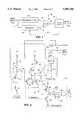
- FIG. 1is a simplified block diagram of the present invention.
- FIG. 2is a detailed schematic diagram of the present invention.
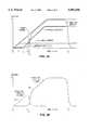
- FIGS. 3A and 3Bare timing diagrams illustrating the operation of the present invention.
- FIG. 1is a block diagram of the subject Level Detection Circuit 10.
- the Input Signal on line 11can be, by way of example, the primary supply voltage V CC for the system. In that event, all of the various elements of the system are also powered by the Input Signal.
- Circuit 10includes a Comparator circuit which compares the output of a Voltage Reference circuit 14 on line 15 and the output of a Translator circuit 16 on line 17. The Translator circuit provides an output indicative of the magnitude of the Input Signal. When the output of the Translator circuit 16 exceeds that of the Voltage Reference 14, the Comparator circuit 12 output on line 13 changes state thereby indicating that the Input Signal is at a predetermined minimum voltage level (trip point level).
- a Pulse Shaper circuit 18converts the output of the Comparator circuit 12 to the Detection Circuit 10 output on line 19 in the form of a pulse suitable for resetting the various logic elements of the associated system powered by Input Signal V CC . All of the elements of the subject Level Detection circuit 10 are typically implemented in a common integrated circuit.
- the function of the Voltage Reference circuit 14is to produce a reference voltage which is relatively independent of the Input Signal V CC . Since the Voltage Reference circuit 14 is powered by the Input Signal in the present example, the output reference voltage will not be produced until the Input Signal reaches some minimum value. To ensure proper operation of the Detection Circuit 10, that minimum value of Input Signal must be less than the trip point level of the Detection Circuit 10.
- the phrase "relatively independent"means that a variation in the Input Signal produces a corresponding variation in the magnitude of the Voltage Reference circuit output which is 30% or less than that of the Input Signal.
- the reference voltage outputcan vary only 15% (0.12 volts) or less (30% of 50%) in order to be considered relatively independent of the Input Signal.
- the Translator circuit 16functions to produce an output signal which is indicative of the magnitude of the Input Signal.
- the magnitude of the output of Translator circuit 16is selected to be equal to that of the Voltage Reference circuit 14 when the Input Signal is at the trip point level.
- FIG. 2is an exemplary implementation of the FIG. 1 circuit.
- the Voltage Reference circuit 14includes a diode-connected P channel transistor 21 connected in series with an N channel transistor 22. As will be explained, when the system is enabled, transistor 22 is conductive so that the drain of transistor 21 is effectively connected to the circuit common. The source and body (N well) of transistor 21 is connected to the Input Signal V CC by way of a resistor 24 for the purpose of powering the Voltage Reference circuit 14. A small parasitic capacitor 23 is associated with resistor 24. The output of the Voltage Reference circuit 14 at the junction of transistor 21 and resistor 24 is connected to one input of Comparator circuit 12 by way of line 15.
- the Translator circuit 16 of FIG. 2includes a pair of N channel transistors 26 and 28 connected in parallel, with the drain of both transistors connected to the Input Signal V CC on line 11.
- the common sources of transistors 26 and 28are connected to one terminal of a resistor 30 and to the remaining input of Comparator circuit 12 by way of line 17.
- the other terminal of resistor 30is connected to the circuit common.
- a small parasitic capacitor 31is associated with resistor 30.
- transistor 26is conductive and transistor 28 is off.
- a voltagewill be generated on line 17 indicative of the magnitude of the Input Signal.
- Transistor 28will be made conductive once the Input Signal reaches the trip point level so as to provide hysteresis, as will also be explained.
- the Comparator circuit 12includes a pair of differentially-connected p channel transistors 32 and 34.
- the common sources of transistors 32 and 34are connected to a tail current source formed by a P channel transistor 36.
- the source of transistor 36is connected to Input Signal V CC for the purpose of powering the Comparator circuit 12.
- Circuit 12includes a current mirror load comprising N channel transistors 38 and 40 having their sources connected to the circuit common.
- Transistor 38is connected as a diode, with the drain and gates connected together and to the drain of input transistor 32.
- Transistor 40has its gate connected to the gate-drain of transistor 38 and its drain connected to the drain of input transistor 34 and to the Comparator circuit output on line 13.
- an N channel transistor 42is connected in parallel with load transistor 38, with transistor 42 being off in normal operation.
- the Pulse Shaper circuit 18includes an inverter circuit 43 comprising a P channel transistor 44 and an N channel transistor 46 with their common gates connected together to receive the output of the Comparator Circuit on line 13.
- the inverter 43is powered by the Input Signal V CC .
- the output of the inverter 43 at the common drain connection of transistors 44 and 46 on line 20is connected to one input of an OR gate 50 by way of inverter 48.
- the output of inverter 48is also connected to the input of a One Shot circuit 52, with the output of the One Shot being connected to another input of OR gate 50.
- One Shot 52is implemented to trigger on a falling edge of the input and produce a fixed duration output pulse.
- the output on line 20is connected to the gate of transistor 28 to provide hysteresis.
- the output of OR gate 19provides the Output of the Level Detection circuit 10 on line 19.
- FIG. 3A timing diagramdepicts five signals, including the Input Signal V CC on line 11, the Voltage Reference circuit output on line 15, the Translator circuit output on line 17, the Comparator circuit output on line 13 and the One Shot circuit 52 output.
- FIG. 3Aillustrates operation when power in the form of voltage V CC , the Input Signal, is first applied at time T 0 . At this point, an ENABLE signal which is active low, is made active so that the Level Detection circuit will perform its normal function.
- the ENABLE signalis made high for the purpose of disabling various one of the system circuits in order to reduce power consumption in certain low power modes of operation.
- the timing diagram of FIG. 3Billustrates the two signals that are logically ORed together to form the Level Detection circuit 10 output on line 19.
- the first signal 54is essentially the output of the Comparator circuit 12 and the second signal 56 is the One Shot output 56.
- the Input Signalis still at ground potential. Since all of the FIG. 2 components are powered by the Input Signal V CC , the remaining four signals of the FIG. 3A timing diagram will also be at ground potential. Further, since signal ENABLE is low, the output of inverter 29 will be high and essentially equal to the magnitude on the Input Signal since inverter 29 is also powered by the Input Signal V CC . As will be explained, transistor 28 is non-conductive at this point. Transistor 26 functions essentially as a source follower circuit with the gate voltage being approximately equal to the Input Signal, with the source voltage following the gate voltage, and with the two voltages differing from one another by a relatively fixed voltage somewhat larger than the threshold voltage of transistor 26. However, at very low Input Signal levels, there is insufficient voltage for transistor 26 to function as a source follower.
- the Input Signalis at a voltage approaching the threshold voltage of transistor 21.
- threshold voltage of a transistoris used here to mean the gate-source voltage required to cause the transistor to conduct a drain-source current of 1 micro-ampere when the drain-source voltage is 1 volt.
- the Voltage Reference output on line 15is at its final value and will thereafter be relatively independent of the Input Signal.
- the Comparator circuit outputwill continue to follow the Input Signal at this point, as also indicated by waveform 54 of FIG. 3B.
- the voltage across the Translator transistor 26will be sufficient for the transistor to become active.
- the Translator signalbegins to increase at the same rate of increase as the Input Signal at this point.
- the output of the Voltage Referenceremains relatively constant and independent of the Input Signal. This independence is enhanced by taking steps to ensure that the gate-source voltage of transistor 21 remains close to the threshold voltage of the transistor. This is done by minimizing the magnitude of the current flow through the transistor which can be achieved by using a large value of resistance for resistor 24.
- a large geometry transistorthat is, a large channel width to channel length ratio (W/L) will help ensure that the gate-source voltage remains close to the threshold voltage.
- the threshold voltage of transistor 21will remain constant and will not change due to the body effect.
- Comparator circuit 12will continue to provide the desired polarity output but will not be fully functional as a comparator until the Input Signal is at least equal to the sum of the threshold voltages of transistors 32 and 38. Up to this point, the magnitude of the Voltage Reference circuit output on line 15 will be larger than that of the Translator circuit 16 output on line 17. Essentially all of the current provided by tail current source transistor 36 will flow through input transistor 34 so that the output of the Comparator circuit 12 on line 13 will be at a "high" level approaching the magnitude of the supply voltage, that is, the magnitude on the Input Signal V CC .
- the output of inverter 43 on line 20will be at a low level. This low level will keep hysteresis transistor 28 in an off state. In addition, the low level will not trigger One Shot 52 and the normally low output of the One Shot will remain low.
- the output of inverter 48will also be high so that one input of OR gate 19 will be high.
- the output of the Level Detection circuit 10will be at a high level, at least as high as the Input Signal V CC will permit at this point in the power on sequence.
- the Input Signalhas reached the predetermined level at which the subject Level Detection circuit 10 was designed to provide a pulse output.
- the Translator outputhas reached the same level as the Voltage Reference output.
- Comparator circuit 12has sufficient gain so that all of the current from tail current source transistor 36 flowing into transistor 34 will switch to transistor 32.
- the output of the Comparator circuit on line 13will switch from a high to a low state approaching the circuit common shortly after time T 3 .
- Inverter 43will invert the Comparator output and the gain of the inverter will increase the rise and fall times of the signal. Inverter 43 will also convert the signal levels to be between approximately ground level and the Input Signal level V CC .
- the output of inverter 43is inverted again by inverter 48 and the falling edge of the output of inverter 48 will trigger One Shot 52.
- One Shot 52will produce a positive output pulse of fixed duration as can be seen in FIG. 3A.
- the One Shot 52 outputis ORed by gate 50 with the output of inverter 48, with this output being similar to the output of Comparator circuit 12 shown in FIG. 3A.
- the combined outputs which form the Detection Circuit 10 outputare shown in the FIG. 3B timing diagram, with waveform 56 representing the contribution made by One Shot 52.
Landscapes
- Measurement Of Current Or Voltage (AREA)
Abstract
Description
Claims (36)
Priority Applications (4)
| Application Number | Priority Date | Filing Date | Title |
|---|---|---|---|
| US08/509,021US5581206A (en) | 1995-07-28 | 1995-07-28 | Power level detection circuit |
| US08/717,702US5767711A (en) | 1995-07-28 | 1996-09-23 | Level detection circuit and method |
| US09/094,825US6046615A (en) | 1995-07-28 | 1998-06-15 | Level detection circuit |
| US09/513,940US6229352B1 (en) | 1995-07-28 | 2000-02-28 | Power level detection circuit |
Applications Claiming Priority (1)
| Application Number | Priority Date | Filing Date | Title |
|---|---|---|---|
| US08/509,021US5581206A (en) | 1995-07-28 | 1995-07-28 | Power level detection circuit |
Related Child Applications (1)
| Application Number | Title | Priority Date | Filing Date |
|---|---|---|---|
| US08/717,702ContinuationUS5767711A (en) | 1995-07-28 | 1996-09-23 | Level detection circuit and method |
Publications (1)
| Publication Number | Publication Date |
|---|---|
| US5581206Atrue US5581206A (en) | 1996-12-03 |
Family
ID=24024985
Family Applications (4)
| Application Number | Title | Priority Date | Filing Date |
|---|---|---|---|
| US08/509,021Expired - LifetimeUS5581206A (en) | 1995-07-28 | 1995-07-28 | Power level detection circuit |
| US08/717,702Expired - LifetimeUS5767711A (en) | 1995-07-28 | 1996-09-23 | Level detection circuit and method |
| US09/094,825Expired - LifetimeUS6046615A (en) | 1995-07-28 | 1998-06-15 | Level detection circuit |
| US09/513,940Expired - LifetimeUS6229352B1 (en) | 1995-07-28 | 2000-02-28 | Power level detection circuit |
Family Applications After (3)
| Application Number | Title | Priority Date | Filing Date |
|---|---|---|---|
| US08/717,702Expired - LifetimeUS5767711A (en) | 1995-07-28 | 1996-09-23 | Level detection circuit and method |
| US09/094,825Expired - LifetimeUS6046615A (en) | 1995-07-28 | 1998-06-15 | Level detection circuit |
| US09/513,940Expired - LifetimeUS6229352B1 (en) | 1995-07-28 | 2000-02-28 | Power level detection circuit |
Country Status (1)
| Country | Link |
|---|---|
| US (4) | US5581206A (en) |
Cited By (53)
| Publication number | Priority date | Publication date | Assignee | Title |
|---|---|---|---|---|
| US5663713A (en)* | 1994-09-08 | 1997-09-02 | Lucas Industries Public Limited Company | Control system |
| US5850156A (en)* | 1996-02-07 | 1998-12-15 | Lucent Technologies Inc. | Processor supervisory circuit and method having increased range of power-on reset signal stability |
| US5875142A (en)* | 1997-06-17 | 1999-02-23 | Micron Technology, Inc. | Integrated circuit with temperature detector |
| US5886935A (en)* | 1997-08-22 | 1999-03-23 | Micron Technology, Inc. | High and negative voltage compare |
| US5898634A (en)* | 1997-06-17 | 1999-04-27 | Micron Technology, Inc. | Integrated circuit with supply voltage detector |
| WO1999030173A1 (en)* | 1997-12-12 | 1999-06-17 | Scenix Semiconductor, Inc. | System and method for programmable brown-out detection and differentiation |
| US5939902A (en)* | 1997-01-30 | 1999-08-17 | Nec Corporation | Integrating circuit internally included in semiconductor device |
| US5956289A (en)* | 1997-06-17 | 1999-09-21 | Micron Technology, Inc. | Clock signal from an adjustable oscillator for an integrated circuit |
| US5966035A (en)* | 1996-05-02 | 1999-10-12 | Integrated Device Technology, Inc. | High voltage tolerable input buffer |
| US6013932A (en)* | 1998-01-07 | 2000-01-11 | Micron Technology, Inc. | Supply voltage reduction circuit for integrated circuit |
| US6018175A (en)* | 1998-09-03 | 2000-01-25 | Micron Technology, Inc. | Gapped-plate capacitor |
| US6020775A (en)* | 1995-07-28 | 2000-02-01 | Micron Technology, Inc. | Adjustable timer circuit |
| US6046615A (en)* | 1995-07-28 | 2000-04-04 | Micron Technology, Inc. | Level detection circuit |
| US6104221A (en)* | 1997-02-05 | 2000-08-15 | Samsung Electronics, Co., Ltd. | Power-up detection circuit of a semiconductor device |
| US6124738A (en)* | 1998-06-09 | 2000-09-26 | Mitsubishi Denki Kabushiki Kaisha | Input buffer for semiconductor device |
| US6184724B1 (en)* | 1998-12-16 | 2001-02-06 | Macronix International Co., Ltd. | Voltage detection circuit |
| US6218893B1 (en)* | 1998-02-19 | 2001-04-17 | Oki Electric Industry Co., Ltd. | Power circuit and clock signal detection circuit |
| US6281723B1 (en)* | 1996-12-19 | 2001-08-28 | Sgs-Thomson Microelectronics S.A. | Device and method for power-on/power-off checking of an integrated circuit |
| US6407598B1 (en)* | 2000-11-08 | 2002-06-18 | Oki Electric Industry Co., Ltd. | Reset pulse signal generating circuit |
| US6501303B1 (en)* | 1999-05-27 | 2002-12-31 | Oki Electric Industry Co., Ltd. | Semiconductor integrated circuit |
| US20030023840A1 (en)* | 2001-07-25 | 2003-01-30 | Micron Technology, Inc. | Power up initialization for memory |
| US6542427B2 (en) | 2001-03-08 | 2003-04-01 | Micron Technology, Inc. | Power validation for memory devices on power up |
| US20050077929A1 (en)* | 2003-08-25 | 2005-04-14 | Infineon Technologies Ag | Driver device, in particular for a semiconductor device, and method for operating a driver device |
| WO2011026148A1 (en)* | 2009-08-31 | 2011-03-03 | Abbott Diabetes Care Inc. | Analyte monitoring system and methods for managing power and noise |
| US8362904B2 (en) | 2007-05-08 | 2013-01-29 | Abbott Diabetes Care Inc. | Analyte monitoring system and methods |
| US8437966B2 (en) | 2003-04-04 | 2013-05-07 | Abbott Diabetes Care Inc. | Method and system for transferring analyte test data |
| US8456301B2 (en) | 2007-05-08 | 2013-06-04 | Abbott Diabetes Care Inc. | Analyte monitoring system and methods |
| US8461985B2 (en) | 2007-05-08 | 2013-06-11 | Abbott Diabetes Care Inc. | Analyte monitoring system and methods |
| US8509107B2 (en) | 2008-05-30 | 2013-08-13 | Abbott Diabetes Care Inc. | Close proximity communication device and methods |
| US8585591B2 (en) | 2005-11-04 | 2013-11-19 | Abbott Diabetes Care Inc. | Method and system for providing basal profile modification in analyte monitoring and management systems |
| US8593109B2 (en) | 2006-03-31 | 2013-11-26 | Abbott Diabetes Care Inc. | Method and system for powering an electronic device |
| US8597575B2 (en) | 2006-03-31 | 2013-12-03 | Abbott Diabetes Care Inc. | Analyte monitoring devices and methods therefor |
| US8597188B2 (en) | 2007-06-21 | 2013-12-03 | Abbott Diabetes Care Inc. | Health management devices and methods |
| US8617069B2 (en) | 2007-06-21 | 2013-12-31 | Abbott Diabetes Care Inc. | Health monitor |
| US8771183B2 (en) | 2004-02-17 | 2014-07-08 | Abbott Diabetes Care Inc. | Method and system for providing data communication in continuous glucose monitoring and management system |
| US9069536B2 (en) | 2011-10-31 | 2015-06-30 | Abbott Diabetes Care Inc. | Electronic devices having integrated reset systems and methods thereof |
| US9088452B2 (en) | 2009-04-29 | 2015-07-21 | Abbott Diabetes Care Inc. | Method and system for providing data communication in continuous glucose monitoring and management system |
| US9095290B2 (en) | 2007-03-01 | 2015-08-04 | Abbott Diabetes Care Inc. | Method and apparatus for providing rolling data in communication systems |
| US9226701B2 (en) | 2009-04-28 | 2016-01-05 | Abbott Diabetes Care Inc. | Error detection in critical repeating data in a wireless sensor system |
| US9314195B2 (en) | 2009-08-31 | 2016-04-19 | Abbott Diabetes Care Inc. | Analyte signal processing device and methods |
| US9532737B2 (en) | 2011-02-28 | 2017-01-03 | Abbott Diabetes Care Inc. | Devices, systems, and methods associated with analyte monitoring devices and devices incorporating the same |
| US9574914B2 (en) | 2007-05-08 | 2017-02-21 | Abbott Diabetes Care Inc. | Method and device for determining elapsed sensor life |
| US9730584B2 (en) | 2003-06-10 | 2017-08-15 | Abbott Diabetes Care Inc. | Glucose measuring device for use in personal area network |
| US9962091B2 (en) | 2002-12-31 | 2018-05-08 | Abbott Diabetes Care Inc. | Continuous glucose monitoring system and methods of use |
| US9968306B2 (en) | 2012-09-17 | 2018-05-15 | Abbott Diabetes Care Inc. | Methods and apparatuses for providing adverse condition notification with enhanced wireless communication range in analyte monitoring systems |
| US9980669B2 (en) | 2011-11-07 | 2018-05-29 | Abbott Diabetes Care Inc. | Analyte monitoring device and methods |
| US10022499B2 (en) | 2007-02-15 | 2018-07-17 | Abbott Diabetes Care Inc. | Device and method for automatic data acquisition and/or detection |
| US10136816B2 (en) | 2009-08-31 | 2018-11-27 | Abbott Diabetes Care Inc. | Medical devices and methods |
| US11006871B2 (en) | 2009-02-03 | 2021-05-18 | Abbott Diabetes Care Inc. | Analyte sensor and apparatus for insertion of the sensor |
| US11793936B2 (en) | 2009-05-29 | 2023-10-24 | Abbott Diabetes Care Inc. | Medical device antenna systems having external antenna configurations |
| US12239463B2 (en) | 2020-08-31 | 2025-03-04 | Abbott Diabetes Care Inc. | Systems, devices, and methods for analyte sensor insertion |
| US12268496B2 (en) | 2017-01-23 | 2025-04-08 | Abbott Diabetes Care Inc. | Systems, devices and methods for analyte sensor insertion |
| US12274548B2 (en) | 2006-10-23 | 2025-04-15 | Abbott Diabetes Care Inc. | Sensor insertion devices and methods of use |
Families Citing this family (27)
| Publication number | Priority date | Publication date | Assignee | Title |
|---|---|---|---|---|
| JP2000036732A (en)* | 1998-07-17 | 2000-02-02 | Mitsubishi Electric Corp | Power-on reset circuit and semiconductor device |
| IT1304117B1 (en)* | 1998-12-17 | 2001-03-07 | St Microelectronics Srl | CURRENT PULSE GENERATOR WITH SYMMETRIC SWITCHING TIMES AND INDEPENDENT OF THE PROCESS AND TEMPERATURE |
| US6459374B1 (en) | 1999-11-12 | 2002-10-01 | Protex International Corp. | Anti-theft computer security system |
| US6362669B1 (en)* | 2000-04-10 | 2002-03-26 | Xilinx, Inc. | Structure and method for initializing IC devices during unstable power-up |
| US6448824B1 (en)* | 2000-09-29 | 2002-09-10 | Intel Corporation | Method and apparatus for integrated circuit power up |
| TW505838B (en)* | 2001-04-04 | 2002-10-11 | Via Tech Inc | Power source detector of digital integrated circuit |
| US7049857B2 (en)* | 2002-01-17 | 2006-05-23 | International Business Machines Corporation | Asymmetric comparator for low power applications |
| US6943596B2 (en)* | 2002-03-12 | 2005-09-13 | Broadcom Corporation | Power-on reset circuit for use in low power supply voltage applications |
| US6677785B1 (en) | 2002-07-24 | 2004-01-13 | Winbond Electronics Corp. | Power level detection circuit |
| KR100487536B1 (en)* | 2002-08-20 | 2005-05-03 | 삼성전자주식회사 | Power-on reset circuit |
| US7030668B1 (en)* | 2003-06-24 | 2006-04-18 | Xilinx, Inc. | Voltage detector |
| US6939608B2 (en)* | 2003-11-19 | 2005-09-06 | Invista North America S.A.R.L. | Bulked continuous filament having a three-sided exterior cross-section and a convex six-sided central void and yarn and carpet produced therefrom |
| US7034579B2 (en)* | 2003-12-22 | 2006-04-25 | Texas Instruments Incorporated | High-speed signal level detector |
| US7057427B2 (en)* | 2004-07-15 | 2006-06-06 | Freescale Semiconductor, Inc | Power on reset circuit |
| WO2006116687A2 (en)* | 2005-04-27 | 2006-11-02 | The Trustees Of The University Of Pennsylvania | Nanoassays |
| US7227388B2 (en)* | 2005-05-09 | 2007-06-05 | Micrel, Incorporated | Propagation delay characteristic comparator circuit |
| US7271624B2 (en)* | 2005-06-29 | 2007-09-18 | Broadcom Corporation | Low-power supply voltage level detection circuit and method |
| US7554607B2 (en)* | 2005-09-20 | 2009-06-30 | National Semiconductor Corporation | Video signal detection circuit |
| JP2008041884A (en)* | 2006-08-04 | 2008-02-21 | Rohm Co Ltd | Semiconductor integrated circuit, and electronic equipment equipped with it |
| US8316158B1 (en) | 2007-03-12 | 2012-11-20 | Cypress Semiconductor Corporation | Configuration of programmable device using a DMA controller |
| KR20090012479A (en)* | 2007-07-30 | 2009-02-04 | 삼성전자주식회사 | Battery module, computer system including same and power control method thereof |
| US7564279B2 (en)* | 2007-10-18 | 2009-07-21 | Micron Technology, Inc. | Power on reset circuitry in electronic systems |
| US7919999B2 (en)* | 2007-10-18 | 2011-04-05 | Micron Technology, Inc. | Band-gap reference voltage detection circuit |
| CN101425031B (en)* | 2007-10-29 | 2010-07-21 | 英业达股份有限公司 | Multi-voltage level detection circuit |
| KR101373005B1 (en)* | 2008-01-04 | 2014-03-14 | 삼성전자주식회사 | Input signal level detection apparatus and method thereof |
| US8228100B2 (en)* | 2010-01-26 | 2012-07-24 | Freescale Semiconductor, Inc. | Data processing system having brown-out detection circuit |
| US8350610B2 (en)* | 2010-07-21 | 2013-01-08 | Intel Corporation | Method and apparatus for fast wake-up of analog biases |
Citations (16)
| Publication number | Priority date | Publication date | Assignee | Title |
|---|---|---|---|---|
| US4041333A (en)* | 1975-12-15 | 1977-08-09 | Intel Corporation | High speed input buffer circuit |
| US4309627A (en)* | 1978-04-14 | 1982-01-05 | Kabushiki Kaisha Daini Seikosha | Detecting circuit for a power source voltage |
| US4437025A (en)* | 1981-07-29 | 1984-03-13 | Intel Corporation | MOS Buffer for receiving TTL level signals |
| US4584492A (en)* | 1984-08-06 | 1986-04-22 | Intel Corporation | Temperature and process stable MOS input buffer |
| US4658156A (en)* | 1983-12-08 | 1987-04-14 | Nec Corporation | Voltage detection circuit for detecting input voltage larger in absolute value than power supply voltage |
| US4922133A (en)* | 1987-07-31 | 1990-05-01 | Kabushiki Kaisha Toshiba | Voltage detecting circuit |
| JPH03206709A (en)* | 1990-01-08 | 1991-09-10 | Nec Corp | Power-on reset circuit |
| US5083045A (en)* | 1987-02-25 | 1992-01-21 | Samsung Electronics Co., Ltd. | High voltage follower and sensing circuit |
| US5097146A (en)* | 1987-04-03 | 1992-03-17 | Sgs Thomson-Microelectronics Sa | Circuit for detecting high voltage level in mos technology |
| US5124590A (en)* | 1991-08-12 | 1992-06-23 | Advanced Micro Devices, Inc. | CMOS tri-mode input buffer |
| US5144159A (en)* | 1990-11-26 | 1992-09-01 | Delco Electronics Corporation | Power-on-reset (POR) circuit having power supply rise time independence |
| US5214316A (en)* | 1991-04-19 | 1993-05-25 | Nec Corporation | Power-on reset circuit device for multi-level power supply sources |
| US5278458A (en)* | 1991-12-13 | 1994-01-11 | Texas Instruments Incorporated | Threshold/voltage detection circuit |
| US5280198A (en)* | 1992-11-06 | 1994-01-18 | Intel Corporation | Power supply level detector |
| US5378936A (en)* | 1991-12-19 | 1995-01-03 | Mitsubishi Denki Kabushiki Kaisha | Voltage level detecting circuit |
| US5469100A (en)* | 1993-06-23 | 1995-11-21 | Sgs Thomson Microelectronics, S.A. | Circuit for the generation of a time-stabilized output pulse |
Family Cites Families (2)
| Publication number | Priority date | Publication date | Assignee | Title |
|---|---|---|---|---|
| JPH04199541A (en) | 1990-11-28 | 1992-07-20 | Mitsubishi Electric Corp | Mode switching circuit |
| US5581206A (en)* | 1995-07-28 | 1996-12-03 | Micron Quantum Devices, Inc. | Power level detection circuit |
- 1995
- 1995-07-28USUS08/509,021patent/US5581206A/ennot_activeExpired - Lifetime
- 1996
- 1996-09-23USUS08/717,702patent/US5767711A/ennot_activeExpired - Lifetime
- 1998
- 1998-06-15USUS09/094,825patent/US6046615A/ennot_activeExpired - Lifetime
- 2000
- 2000-02-28USUS09/513,940patent/US6229352B1/ennot_activeExpired - Lifetime
Patent Citations (16)
| Publication number | Priority date | Publication date | Assignee | Title |
|---|---|---|---|---|
| US4041333A (en)* | 1975-12-15 | 1977-08-09 | Intel Corporation | High speed input buffer circuit |
| US4309627A (en)* | 1978-04-14 | 1982-01-05 | Kabushiki Kaisha Daini Seikosha | Detecting circuit for a power source voltage |
| US4437025A (en)* | 1981-07-29 | 1984-03-13 | Intel Corporation | MOS Buffer for receiving TTL level signals |
| US4658156A (en)* | 1983-12-08 | 1987-04-14 | Nec Corporation | Voltage detection circuit for detecting input voltage larger in absolute value than power supply voltage |
| US4584492A (en)* | 1984-08-06 | 1986-04-22 | Intel Corporation | Temperature and process stable MOS input buffer |
| US5083045A (en)* | 1987-02-25 | 1992-01-21 | Samsung Electronics Co., Ltd. | High voltage follower and sensing circuit |
| US5097146A (en)* | 1987-04-03 | 1992-03-17 | Sgs Thomson-Microelectronics Sa | Circuit for detecting high voltage level in mos technology |
| US4922133A (en)* | 1987-07-31 | 1990-05-01 | Kabushiki Kaisha Toshiba | Voltage detecting circuit |
| JPH03206709A (en)* | 1990-01-08 | 1991-09-10 | Nec Corp | Power-on reset circuit |
| US5144159A (en)* | 1990-11-26 | 1992-09-01 | Delco Electronics Corporation | Power-on-reset (POR) circuit having power supply rise time independence |
| US5214316A (en)* | 1991-04-19 | 1993-05-25 | Nec Corporation | Power-on reset circuit device for multi-level power supply sources |
| US5124590A (en)* | 1991-08-12 | 1992-06-23 | Advanced Micro Devices, Inc. | CMOS tri-mode input buffer |
| US5278458A (en)* | 1991-12-13 | 1994-01-11 | Texas Instruments Incorporated | Threshold/voltage detection circuit |
| US5378936A (en)* | 1991-12-19 | 1995-01-03 | Mitsubishi Denki Kabushiki Kaisha | Voltage level detecting circuit |
| US5280198A (en)* | 1992-11-06 | 1994-01-18 | Intel Corporation | Power supply level detector |
| US5469100A (en)* | 1993-06-23 | 1995-11-21 | Sgs Thomson Microelectronics, S.A. | Circuit for the generation of a time-stabilized output pulse |
Cited By (138)
| Publication number | Priority date | Publication date | Assignee | Title |
|---|---|---|---|---|
| US5663713A (en)* | 1994-09-08 | 1997-09-02 | Lucas Industries Public Limited Company | Control system |
| US6229352B1 (en) | 1995-07-28 | 2001-05-08 | Micron Technology, Inc. | Power level detection circuit |
| US6046615A (en)* | 1995-07-28 | 2000-04-04 | Micron Technology, Inc. | Level detection circuit |
| US6020775A (en)* | 1995-07-28 | 2000-02-01 | Micron Technology, Inc. | Adjustable timer circuit |
| US5850156A (en)* | 1996-02-07 | 1998-12-15 | Lucent Technologies Inc. | Processor supervisory circuit and method having increased range of power-on reset signal stability |
| US5966035A (en)* | 1996-05-02 | 1999-10-12 | Integrated Device Technology, Inc. | High voltage tolerable input buffer |
| US6441651B2 (en) | 1996-05-02 | 2002-08-27 | Integrated Device Technology, Inc. | High voltage tolerable input buffer |
| US6104229A (en)* | 1996-05-02 | 2000-08-15 | Integrated Device Technology, Inc. | High voltage tolerable input buffer and method for operating same |
| US6281723B1 (en)* | 1996-12-19 | 2001-08-28 | Sgs-Thomson Microelectronics S.A. | Device and method for power-on/power-off checking of an integrated circuit |
| US5939902A (en)* | 1997-01-30 | 1999-08-17 | Nec Corporation | Integrating circuit internally included in semiconductor device |
| US6104221A (en)* | 1997-02-05 | 2000-08-15 | Samsung Electronics, Co., Ltd. | Power-up detection circuit of a semiconductor device |
| US5875142A (en)* | 1997-06-17 | 1999-02-23 | Micron Technology, Inc. | Integrated circuit with temperature detector |
| US5956289A (en)* | 1997-06-17 | 1999-09-21 | Micron Technology, Inc. | Clock signal from an adjustable oscillator for an integrated circuit |
| US5898634A (en)* | 1997-06-17 | 1999-04-27 | Micron Technology, Inc. | Integrated circuit with supply voltage detector |
| US6002627A (en)* | 1997-06-17 | 1999-12-14 | Micron Technology, Inc. | Integrated circuit with temperature detector |
| US6160755A (en)* | 1997-06-17 | 2000-12-12 | Micron Technology, Inc. | Clock signal from an adjustable oscillator for an integrated circuit |
| US6034906A (en)* | 1997-08-22 | 2000-03-07 | Micron Technology, Inc. | High and negative voltage compare |
| US5886935A (en)* | 1997-08-22 | 1999-03-23 | Micron Technology, Inc. | High and negative voltage compare |
| WO1999030173A1 (en)* | 1997-12-12 | 1999-06-17 | Scenix Semiconductor, Inc. | System and method for programmable brown-out detection and differentiation |
| US5943635A (en)* | 1997-12-12 | 1999-08-24 | Scenix Semiconductor Inc. | System and method for programmable brown-out detection and differentiation |
| US20020033722A1 (en)* | 1998-01-07 | 2002-03-21 | Micron Technology, Inc. | Supply voltage reduction circuit for integrated circuit |
| US6867464B2 (en) | 1998-01-07 | 2005-03-15 | Micron Technology Inc. | Supply voltage reduction circuit for integrated circuit |
| US6291862B1 (en) | 1998-01-07 | 2001-09-18 | Micron Technology, Inc. | Supply voltage reduction circuit for integrated circuit |
| US6013932A (en)* | 1998-01-07 | 2000-01-11 | Micron Technology, Inc. | Supply voltage reduction circuit for integrated circuit |
| US6218893B1 (en)* | 1998-02-19 | 2001-04-17 | Oki Electric Industry Co., Ltd. | Power circuit and clock signal detection circuit |
| US6124738A (en)* | 1998-06-09 | 2000-09-26 | Mitsubishi Denki Kabushiki Kaisha | Input buffer for semiconductor device |
| US20040264104A1 (en)* | 1998-09-03 | 2004-12-30 | Kao David Y. | Gapped-plate capacitor |
| US6316326B1 (en) | 1998-09-03 | 2001-11-13 | Micron Technology, Inc. | Gapped-plate capacitor |
| US6498363B1 (en) | 1998-09-03 | 2002-12-24 | Micron Technology, Inc. | Gapped-plate capacitor |
| US20070058325A1 (en)* | 1998-09-03 | 2007-03-15 | Micron Technology, Inc. | Gapped-plate capacitor |
| US7151659B2 (en) | 1998-09-03 | 2006-12-19 | Micron Technology, Inc. | Gapped-plate capacitor |
| US6958901B2 (en) | 1998-09-03 | 2005-10-25 | Micron Technology, Inc. | Gapped-plate capacitor |
| US20030075751A1 (en)* | 1998-09-03 | 2003-04-24 | Kao David Y. | Gapped-plate capacitor |
| US20050121740A1 (en)* | 1998-09-03 | 2005-06-09 | Kao David Y. | Gapped-plate capacitor |
| US6774421B2 (en) | 1998-09-03 | 2004-08-10 | Micron Technology, Inc. | Gapped-plate capacitor |
| US6018175A (en)* | 1998-09-03 | 2000-01-25 | Micron Technology, Inc. | Gapped-plate capacitor |
| US6184724B1 (en)* | 1998-12-16 | 2001-02-06 | Macronix International Co., Ltd. | Voltage detection circuit |
| US6501303B1 (en)* | 1999-05-27 | 2002-12-31 | Oki Electric Industry Co., Ltd. | Semiconductor integrated circuit |
| US6407598B1 (en)* | 2000-11-08 | 2002-06-18 | Oki Electric Industry Co., Ltd. | Reset pulse signal generating circuit |
| US6731562B2 (en) | 2001-03-08 | 2004-05-04 | Micron Technology, Inc. | Power validation for memory devices on power up |
| US20030067831A1 (en)* | 2001-03-08 | 2003-04-10 | Micron Technology, Inc. | Power validation for memory devices on power up |
| US6542427B2 (en) | 2001-03-08 | 2003-04-01 | Micron Technology, Inc. | Power validation for memory devices on power up |
| US7774536B2 (en) | 2001-07-25 | 2010-08-10 | Micron Technology, Inc. | Power up initialization for memory |
| US7036004B2 (en) | 2001-07-25 | 2006-04-25 | Micron Technology, Inc. | Power up initialization for memory |
| US20060184782A1 (en)* | 2001-07-25 | 2006-08-17 | Micron Technology, Inc. | Power up initialization for memory |
| US20030023840A1 (en)* | 2001-07-25 | 2003-01-30 | Micron Technology, Inc. | Power up initialization for memory |
| US9962091B2 (en) | 2002-12-31 | 2018-05-08 | Abbott Diabetes Care Inc. | Continuous glucose monitoring system and methods of use |
| US10750952B2 (en) | 2002-12-31 | 2020-08-25 | Abbott Diabetes Care Inc. | Continuous glucose monitoring system and methods of use |
| US10039881B2 (en) | 2002-12-31 | 2018-08-07 | Abbott Diabetes Care Inc. | Method and system for providing data communication in continuous glucose monitoring and management system |
| US8483974B2 (en) | 2003-04-04 | 2013-07-09 | Abbott Diabetes Care Inc. | Method and system for transferring analyte test data |
| US8437966B2 (en) | 2003-04-04 | 2013-05-07 | Abbott Diabetes Care Inc. | Method and system for transferring analyte test data |
| US8682598B2 (en) | 2003-04-04 | 2014-03-25 | Abbott Laboratories | Method and system for transferring analyte test data |
| US8560250B2 (en) | 2003-04-04 | 2013-10-15 | Abbott Laboratories | Method and system for transferring analyte test data |
| US9730584B2 (en) | 2003-06-10 | 2017-08-15 | Abbott Diabetes Care Inc. | Glucose measuring device for use in personal area network |
| US7486116B2 (en)* | 2003-08-25 | 2009-02-03 | Infineon Technologies Ag | Driver device, in particular for a semiconductor device, and method for operating a driver device |
| US20050077929A1 (en)* | 2003-08-25 | 2005-04-14 | Infineon Technologies Ag | Driver device, in particular for a semiconductor device, and method for operating a driver device |
| US8771183B2 (en) | 2004-02-17 | 2014-07-08 | Abbott Diabetes Care Inc. | Method and system for providing data communication in continuous glucose monitoring and management system |
| US11538580B2 (en) | 2005-11-04 | 2022-12-27 | Abbott Diabetes Care Inc. | Method and system for providing basal profile modification in analyte monitoring and management systems |
| US9323898B2 (en) | 2005-11-04 | 2016-04-26 | Abbott Diabetes Care Inc. | Method and system for providing basal profile modification in analyte monitoring and management systems |
| US9669162B2 (en) | 2005-11-04 | 2017-06-06 | Abbott Diabetes Care Inc. | Method and system for providing basal profile modification in analyte monitoring and management systems |
| US8585591B2 (en) | 2005-11-04 | 2013-11-19 | Abbott Diabetes Care Inc. | Method and system for providing basal profile modification in analyte monitoring and management systems |
| US8597575B2 (en) | 2006-03-31 | 2013-12-03 | Abbott Diabetes Care Inc. | Analyte monitoring devices and methods therefor |
| US9743863B2 (en) | 2006-03-31 | 2017-08-29 | Abbott Diabetes Care Inc. | Method and system for powering an electronic device |
| US8593109B2 (en) | 2006-03-31 | 2013-11-26 | Abbott Diabetes Care Inc. | Method and system for powering an electronic device |
| US8933664B2 (en) | 2006-03-31 | 2015-01-13 | Abbott Diabetes Care Inc. | Method and system for powering an electronic device |
| US9039975B2 (en) | 2006-03-31 | 2015-05-26 | Abbott Diabetes Care Inc. | Analyte monitoring devices and methods therefor |
| US9625413B2 (en) | 2006-03-31 | 2017-04-18 | Abbott Diabetes Care Inc. | Analyte monitoring devices and methods therefor |
| US9380971B2 (en) | 2006-03-31 | 2016-07-05 | Abbott Diabetes Care Inc. | Method and system for powering an electronic device |
| US12274548B2 (en) | 2006-10-23 | 2025-04-15 | Abbott Diabetes Care Inc. | Sensor insertion devices and methods of use |
| US10022499B2 (en) | 2007-02-15 | 2018-07-17 | Abbott Diabetes Care Inc. | Device and method for automatic data acquisition and/or detection |
| US10617823B2 (en) | 2007-02-15 | 2020-04-14 | Abbott Diabetes Care Inc. | Device and method for automatic data acquisition and/or detection |
| US9801545B2 (en) | 2007-03-01 | 2017-10-31 | Abbott Diabetes Care Inc. | Method and apparatus for providing rolling data in communication systems |
| US9095290B2 (en) | 2007-03-01 | 2015-08-04 | Abbott Diabetes Care Inc. | Method and apparatus for providing rolling data in communication systems |
| US9000929B2 (en) | 2007-05-08 | 2015-04-07 | Abbott Diabetes Care Inc. | Analyte monitoring system and methods |
| US9949678B2 (en) | 2007-05-08 | 2018-04-24 | Abbott Diabetes Care Inc. | Method and device for determining elapsed sensor life |
| US12396645B2 (en) | 2007-05-08 | 2025-08-26 | Abbott Diabetes Care Inc. | Analyte monitoring system and methods |
| US12357180B2 (en) | 2007-05-08 | 2025-07-15 | Abbott Diabetes Care Inc. | Analyte monitoring system and methods |
| US9314198B2 (en) | 2007-05-08 | 2016-04-19 | Abbott Diabetes Care Inc. | Analyte monitoring system and methods |
| US9177456B2 (en) | 2007-05-08 | 2015-11-03 | Abbott Diabetes Care Inc. | Analyte monitoring system and methods |
| US11696684B2 (en) | 2007-05-08 | 2023-07-11 | Abbott Diabetes Care Inc. | Analyte monitoring system and methods |
| US8362904B2 (en) | 2007-05-08 | 2013-01-29 | Abbott Diabetes Care Inc. | Analyte monitoring system and methods |
| US10952611B2 (en) | 2007-05-08 | 2021-03-23 | Abbott Diabetes Care Inc. | Analyte monitoring system and methods |
| US9574914B2 (en) | 2007-05-08 | 2017-02-21 | Abbott Diabetes Care Inc. | Method and device for determining elapsed sensor life |
| US8456301B2 (en) | 2007-05-08 | 2013-06-04 | Abbott Diabetes Care Inc. | Analyte monitoring system and methods |
| US9649057B2 (en) | 2007-05-08 | 2017-05-16 | Abbott Diabetes Care Inc. | Analyte monitoring system and methods |
| US9035767B2 (en) | 2007-05-08 | 2015-05-19 | Abbott Diabetes Care Inc. | Analyte monitoring system and methods |
| US10653317B2 (en) | 2007-05-08 | 2020-05-19 | Abbott Diabetes Care Inc. | Analyte monitoring system and methods |
| US8461985B2 (en) | 2007-05-08 | 2013-06-11 | Abbott Diabetes Care Inc. | Analyte monitoring system and methods |
| US10178954B2 (en) | 2007-05-08 | 2019-01-15 | Abbott Diabetes Care Inc. | Analyte monitoring system and methods |
| US8593287B2 (en) | 2007-05-08 | 2013-11-26 | Abbott Diabetes Care Inc. | Analyte monitoring system and methods |
| US8617069B2 (en) | 2007-06-21 | 2013-12-31 | Abbott Diabetes Care Inc. | Health monitor |
| US11264133B2 (en) | 2007-06-21 | 2022-03-01 | Abbott Diabetes Care Inc. | Health management devices and methods |
| US8597188B2 (en) | 2007-06-21 | 2013-12-03 | Abbott Diabetes Care Inc. | Health management devices and methods |
| US11276492B2 (en) | 2007-06-21 | 2022-03-15 | Abbott Diabetes Care Inc. | Health management devices and methods |
| US8737259B2 (en) | 2008-05-30 | 2014-05-27 | Abbott Diabetes Care Inc. | Close proximity communication device and methods |
| US11770210B2 (en) | 2008-05-30 | 2023-09-26 | Abbott Diabetes Care Inc. | Close proximity communication device and methods |
| US12368529B2 (en) | 2008-05-30 | 2025-07-22 | Abbott Diabetes Care Inc. | Close proximity communication device and methods |
| US9184875B2 (en) | 2008-05-30 | 2015-11-10 | Abbott Diabetes Care, Inc. | Close proximity communication device and methods |
| US8509107B2 (en) | 2008-05-30 | 2013-08-13 | Abbott Diabetes Care Inc. | Close proximity communication device and methods |
| US9831985B2 (en) | 2008-05-30 | 2017-11-28 | Abbott Diabetes Care Inc. | Close proximity communication device and methods |
| US11006871B2 (en) | 2009-02-03 | 2021-05-18 | Abbott Diabetes Care Inc. | Analyte sensor and apparatus for insertion of the sensor |
| US11166656B2 (en) | 2009-02-03 | 2021-11-09 | Abbott Diabetes Care Inc. | Analyte sensor and apparatus for insertion of the sensor |
| US11213229B2 (en) | 2009-02-03 | 2022-01-04 | Abbott Diabetes Care Inc. | Analyte sensor and apparatus for insertion of the sensor |
| US11006872B2 (en) | 2009-02-03 | 2021-05-18 | Abbott Diabetes Care Inc. | Analyte sensor and apparatus for insertion of the sensor |
| US11006870B2 (en) | 2009-02-03 | 2021-05-18 | Abbott Diabetes Care Inc. | Analyte sensor and apparatus for insertion of the sensor |
| US11202591B2 (en) | 2009-02-03 | 2021-12-21 | Abbott Diabetes Care Inc. | Analyte sensor and apparatus for insertion of the sensor |
| US9226701B2 (en) | 2009-04-28 | 2016-01-05 | Abbott Diabetes Care Inc. | Error detection in critical repeating data in a wireless sensor system |
| US9088452B2 (en) | 2009-04-29 | 2015-07-21 | Abbott Diabetes Care Inc. | Method and system for providing data communication in continuous glucose monitoring and management system |
| US10172518B2 (en) | 2009-04-29 | 2019-01-08 | Abbott Diabetes Care Inc. | Method and system for providing data communication in continuous glucose monitoring and management system |
| US9693688B2 (en) | 2009-04-29 | 2017-07-04 | Abbott Diabetes Care Inc. | Method and system for providing data communication in continuous glucose monitoring and management system |
| US10617296B2 (en) | 2009-04-29 | 2020-04-14 | Abbott Diabetes Care Inc. | Method and system for providing data communication in continuous glucose monitoring and management system |
| US9949639B2 (en) | 2009-04-29 | 2018-04-24 | Abbott Diabetes Care Inc. | Method and system for providing data communication in continuous glucose monitoring and management system |
| US12364815B2 (en) | 2009-05-29 | 2025-07-22 | Abbott Diabetes Care Inc. | Medical device antenna systems having external antenna configurations |
| US11793936B2 (en) | 2009-05-29 | 2023-10-24 | Abbott Diabetes Care Inc. | Medical device antenna systems having external antenna configurations |
| US11872370B2 (en) | 2009-05-29 | 2024-01-16 | Abbott Diabetes Care Inc. | Medical device antenna systems having external antenna configurations |
| US10429250B2 (en) | 2009-08-31 | 2019-10-01 | Abbott Diabetes Care, Inc. | Analyte monitoring system and methods for managing power and noise |
| US10136816B2 (en) | 2009-08-31 | 2018-11-27 | Abbott Diabetes Care Inc. | Medical devices and methods |
| US11045147B2 (en) | 2009-08-31 | 2021-06-29 | Abbott Diabetes Care Inc. | Analyte signal processing device and methods |
| US9968302B2 (en) | 2009-08-31 | 2018-05-15 | Abbott Diabetes Care Inc. | Analyte signal processing device and methods |
| US9314195B2 (en) | 2009-08-31 | 2016-04-19 | Abbott Diabetes Care Inc. | Analyte signal processing device and methods |
| US12315630B2 (en) | 2009-08-31 | 2025-05-27 | Abbott Diabetes Care Inc. | Medical devices and methods |
| US11635332B2 (en) | 2009-08-31 | 2023-04-25 | Abbott Diabetes Care Inc. | Analyte monitoring system and methods for managing power and noise |
| US12279894B2 (en) | 2009-08-31 | 2025-04-22 | Abbott Diabetes Care Inc. | Analyte signal processing device and methods |
| US8993331B2 (en) | 2009-08-31 | 2015-03-31 | Abbott Diabetes Care Inc. | Analyte monitoring system and methods for managing power and noise |
| US10492685B2 (en) | 2009-08-31 | 2019-12-03 | Abbott Diabetes Care Inc. | Medical devices and methods |
| USD1010133S1 (en) | 2009-08-31 | 2024-01-02 | Abbott Diabetes Care Inc. | Analyte sensor assembly |
| US11150145B2 (en) | 2009-08-31 | 2021-10-19 | Abbott Diabetes Care Inc. | Analyte monitoring system and methods for managing power and noise |
| WO2011026148A1 (en)* | 2009-08-31 | 2011-03-03 | Abbott Diabetes Care Inc. | Analyte monitoring system and methods for managing power and noise |
| US9532737B2 (en) | 2011-02-28 | 2017-01-03 | Abbott Diabetes Care Inc. | Devices, systems, and methods associated with analyte monitoring devices and devices incorporating the same |
| US9069536B2 (en) | 2011-10-31 | 2015-06-30 | Abbott Diabetes Care Inc. | Electronic devices having integrated reset systems and methods thereof |
| US9465420B2 (en) | 2011-10-31 | 2016-10-11 | Abbott Diabetes Care Inc. | Electronic devices having integrated reset systems and methods thereof |
| US9980669B2 (en) | 2011-11-07 | 2018-05-29 | Abbott Diabetes Care Inc. | Analyte monitoring device and methods |
| US11950936B2 (en) | 2012-09-17 | 2024-04-09 | Abbott Diabetes Care Inc. | Methods and apparatuses for providing adverse condition notification with enhanced wireless communication range in analyte monitoring systems |
| US11612363B2 (en) | 2012-09-17 | 2023-03-28 | Abbott Diabetes Care Inc. | Methods and apparatuses for providing adverse condition notification with enhanced wireless communication range in analyte monitoring systems |
| US9968306B2 (en) | 2012-09-17 | 2018-05-15 | Abbott Diabetes Care Inc. | Methods and apparatuses for providing adverse condition notification with enhanced wireless communication range in analyte monitoring systems |
| US12419589B2 (en) | 2012-09-17 | 2025-09-23 | Abbott Diabetes Care Inc. | Methods and apparatuses for providing adverse condition notification with enhanced wireless communication range in analyte monitoring systems |
| US12268496B2 (en) | 2017-01-23 | 2025-04-08 | Abbott Diabetes Care Inc. | Systems, devices and methods for analyte sensor insertion |
| US12239463B2 (en) | 2020-08-31 | 2025-03-04 | Abbott Diabetes Care Inc. | Systems, devices, and methods for analyte sensor insertion |
Also Published As
| Publication number | Publication date |
|---|---|
| US6229352B1 (en) | 2001-05-08 |
| US5767711A (en) | 1998-06-16 |
| US6046615A (en) | 2000-04-04 |
Similar Documents
| Publication | Publication Date | Title |
|---|---|---|
| US5581206A (en) | Power level detection circuit | |
| US5144159A (en) | Power-on-reset (POR) circuit having power supply rise time independence | |
| US5760624A (en) | Power-on reset circuit with hysteresis | |
| US4812679A (en) | Power-on reset circuit | |
| US5440254A (en) | Accurate low voltage detect circuit | |
| US4142118A (en) | Integrated circuit with power supply voltage level detection | |
| JP3756961B2 (en) | Chip initialization signal generation circuit for semiconductor memory device | |
| US6809565B2 (en) | Semiconductor device | |
| US7034581B2 (en) | Voltage detecting circuit | |
| JPH05168151A (en) | Power-on detection circuit | |
| EP0887935A1 (en) | Noise isolation circuit | |
| US5602502A (en) | Circuit for detecting when a supply output voltage exceeds a predetermined level | |
| JP2001160743A (en) | Active undershoot enhanced FET switch | |
| JPH04345208A (en) | Power-on reset circuit | |
| JP2983460B2 (en) | Power supply detection circuit | |
| KR950035091A (en) | Semiconductor integrated circuit | |
| US6989704B2 (en) | Delay circuit having function of filter circuit | |
| US6037827A (en) | Noise isolation circuit | |
| JPH0736516B2 (en) | Power-on reset circuit | |
| JPH0611102B2 (en) | Signal detection circuit | |
| KR100323987B1 (en) | Integrated circuit | |
| US7372321B2 (en) | Robust start-up circuit and method for on-chip self-biased voltage and/or current reference | |
| US5686848A (en) | Power-up/power-down reset circuit for low voltage interval | |
| JPH06204832A (en) | Circuit for sensing buildup of power supply | |
| US6377080B1 (en) | Dynamic logic circuit |
Legal Events
| Date | Code | Title | Description |
|---|---|---|---|
| AS | Assignment | Owner name:MICRON QUANTUM DEVICES, INC., CALIFORNIA Free format text:ASSIGNMENT OF ASSIGNORS INTEREST;ASSIGNOR:CHEVALLIER, CHRISTOPHE J.;REEL/FRAME:007645/0556 Effective date:19950629 | |
| FEPP | Fee payment procedure | Free format text:PAYOR NUMBER ASSIGNED (ORIGINAL EVENT CODE: ASPN); ENTITY STATUS OF PATENT OWNER: LARGE ENTITY | |
| STCF | Information on status: patent grant | Free format text:PATENTED CASE | |
| FPAY | Fee payment | Year of fee payment:4 | |
| FPAY | Fee payment | Year of fee payment:8 | |
| FPAY | Fee payment | Year of fee payment:12 | |
| AS | Assignment | Owner name:MICRON TECHNOLOGY, INC., IDAHO Free format text:MERGER;ASSIGNOR:MICRON QUANTUM DEVICES, INC.;REEL/FRAME:029445/0165 Effective date:19980120 | |
| AS | Assignment | Owner name:U.S. BANK NATIONAL ASSOCIATION, AS COLLATERAL AGENT, CALIFORNIA Free format text:SECURITY INTEREST;ASSIGNOR:MICRON TECHNOLOGY, INC.;REEL/FRAME:038669/0001 Effective date:20160426 Owner name:U.S. BANK NATIONAL ASSOCIATION, AS COLLATERAL AGEN Free format text:SECURITY INTEREST;ASSIGNOR:MICRON TECHNOLOGY, INC.;REEL/FRAME:038669/0001 Effective date:20160426 | |
| AS | Assignment | Owner name:MORGAN STANLEY SENIOR FUNDING, INC., AS COLLATERAL AGENT, MARYLAND Free format text:PATENT SECURITY AGREEMENT;ASSIGNOR:MICRON TECHNOLOGY, INC.;REEL/FRAME:038954/0001 Effective date:20160426 Owner name:MORGAN STANLEY SENIOR FUNDING, INC., AS COLLATERAL Free format text:PATENT SECURITY AGREEMENT;ASSIGNOR:MICRON TECHNOLOGY, INC.;REEL/FRAME:038954/0001 Effective date:20160426 | |
| AS | Assignment | Owner name:U.S. BANK NATIONAL ASSOCIATION, AS COLLATERAL AGENT, CALIFORNIA Free format text:CORRECTIVE ASSIGNMENT TO CORRECT THE REPLACE ERRONEOUSLY FILED PATENT #7358718 WITH THE CORRECT PATENT #7358178 PREVIOUSLY RECORDED ON REEL 038669 FRAME 0001. ASSIGNOR(S) HEREBY CONFIRMS THE SECURITY INTEREST;ASSIGNOR:MICRON TECHNOLOGY, INC.;REEL/FRAME:043079/0001 Effective date:20160426 Owner name:U.S. BANK NATIONAL ASSOCIATION, AS COLLATERAL AGEN Free format text:CORRECTIVE ASSIGNMENT TO CORRECT THE REPLACE ERRONEOUSLY FILED PATENT #7358718 WITH THE CORRECT PATENT #7358178 PREVIOUSLY RECORDED ON REEL 038669 FRAME 0001. ASSIGNOR(S) HEREBY CONFIRMS THE SECURITY INTEREST;ASSIGNOR:MICRON TECHNOLOGY, INC.;REEL/FRAME:043079/0001 Effective date:20160426 | |
| AS | Assignment | Owner name:JPMORGAN CHASE BANK, N.A., AS COLLATERAL AGENT, ILLINOIS Free format text:SECURITY INTEREST;ASSIGNORS:MICRON TECHNOLOGY, INC.;MICRON SEMICONDUCTOR PRODUCTS, INC.;REEL/FRAME:047540/0001 Effective date:20180703 Owner name:JPMORGAN CHASE BANK, N.A., AS COLLATERAL AGENT, IL Free format text:SECURITY INTEREST;ASSIGNORS:MICRON TECHNOLOGY, INC.;MICRON SEMICONDUCTOR PRODUCTS, INC.;REEL/FRAME:047540/0001 Effective date:20180703 | |
| AS | Assignment | Owner name:MICRON TECHNOLOGY, INC., IDAHO Free format text:RELEASE BY SECURED PARTY;ASSIGNOR:U.S. BANK NATIONAL ASSOCIATION, AS COLLATERAL AGENT;REEL/FRAME:047243/0001 Effective date:20180629 | |
| AS | Assignment | Owner name:MICRON TECHNOLOGY, INC., IDAHO Free format text:RELEASE BY SECURED PARTY;ASSIGNOR:MORGAN STANLEY SENIOR FUNDING, INC., AS COLLATERAL AGENT;REEL/FRAME:050937/0001 Effective date:20190731 | |
| AS | Assignment | Owner name:MICRON TECHNOLOGY, INC., IDAHO Free format text:RELEASE BY SECURED PARTY;ASSIGNOR:JPMORGAN CHASE BANK, N.A., AS COLLATERAL AGENT;REEL/FRAME:051028/0001 Effective date:20190731 Owner name:MICRON SEMICONDUCTOR PRODUCTS, INC., IDAHO Free format text:RELEASE BY SECURED PARTY;ASSIGNOR:JPMORGAN CHASE BANK, N.A., AS COLLATERAL AGENT;REEL/FRAME:051028/0001 Effective date:20190731 |