US5580385A - Structure and method for incorporating an inductively coupled plasma source in a plasma processing chamber - Google Patents
Structure and method for incorporating an inductively coupled plasma source in a plasma processing chamberDownload PDFInfo
- Publication number
- US5580385A US5580385AUS08/269,414US26941494AUS5580385AUS 5580385 AUS5580385 AUS 5580385AUS 26941494 AUS26941494 AUS 26941494AUS 5580385 AUS5580385 AUS 5580385A
- Authority
- US
- United States
- Prior art keywords
- antenna
- processing chamber
- plasma processing
- plasma
- housing
- Prior art date
- Legal status (The legal status is an assumption and is not a legal conclusion. Google has not performed a legal analysis and makes no representation as to the accuracy of the status listed.)
- Expired - Lifetime
Links
- 238000000034methodMethods0.000titleclaimsabstractdescription30
- 238000009616inductively coupled plasmaMethods0.000titleclaimsabstractdescription24
- 230000008569processEffects0.000claimsabstractdescription19
- 239000004593EpoxySubstances0.000claimsabstractdescription14
- 230000015572biosynthetic processEffects0.000claimsabstractdescription8
- 239000008393encapsulating agentSubstances0.000claimsdescription4
- 238000007789sealingMethods0.000claimsdescription4
- 239000003990capacitorSubstances0.000claimsdescription3
- 125000006850spacer groupChemical group0.000claimsdescription2
- 239000012212insulatorSubstances0.000claims2
- 238000009826distributionMethods0.000abstractdescription15
- 239000007789gasSubstances0.000abstractdescription11
- 210000002381plasmaAnatomy0.000description64
- 235000012431wafersNutrition0.000description32
- 230000004907fluxEffects0.000description21
- 230000000694effectsEffects0.000description15
- 230000008901benefitEffects0.000description9
- 230000005684electric fieldEffects0.000description7
- 230000008878couplingEffects0.000description6
- 238000010168coupling processMethods0.000description6
- 238000005859coupling reactionMethods0.000description6
- 230000005672electromagnetic fieldEffects0.000description5
- BSYNRYMUTXBXSQ-UHFFFAOYSA-NAspirinChemical compoundCC(=O)OC1=CC=CC=C1C(O)=OBSYNRYMUTXBXSQ-UHFFFAOYSA-N0.000description4
- 241001364096PachycephalidaeSpecies0.000description4
- 238000010438heat treatmentMethods0.000description4
- 238000004519manufacturing processMethods0.000description4
- 229910052782aluminiumInorganic materials0.000description3
- XAGFODPZIPBFFR-UHFFFAOYSA-NaluminiumChemical compound[Al]XAGFODPZIPBFFR-UHFFFAOYSA-N0.000description3
- 239000000919ceramicSubstances0.000description3
- 238000004088simulationMethods0.000description3
- XKRFYHLGVUSROY-UHFFFAOYSA-NArgonChemical compound[Ar]XKRFYHLGVUSROY-UHFFFAOYSA-N0.000description2
- 230000003247decreasing effectEffects0.000description2
- 238000010586diagramMethods0.000description2
- 230000006698inductionEffects0.000description2
- 230000003993interactionEffects0.000description2
- 239000000463materialSubstances0.000description2
- 229910052751metalInorganic materials0.000description2
- 239000002184metalSubstances0.000description2
- 238000005457optimizationMethods0.000description2
- 235000012771pancakesNutrition0.000description2
- 230000004075alterationEffects0.000description1
- 229910052786argonInorganic materials0.000description1
- 230000009286beneficial effectEffects0.000description1
- 230000002860competitive effectEffects0.000description1
- 230000005686electrostatic fieldEffects0.000description1
- 125000003700epoxy groupChemical group0.000description1
- 238000005530etchingMethods0.000description1
- 238000007667floatingMethods0.000description1
- 238000005259measurementMethods0.000description1
- 230000007246mechanismEffects0.000description1
- 238000013386optimize processMethods0.000description1
- 239000002245particleSubstances0.000description1
- 238000001020plasma etchingMethods0.000description1
- 229920000647polyepoxidePolymers0.000description1
- 238000005086pumpingMethods0.000description1
- 239000010453quartzSubstances0.000description1
- 239000004065semiconductorSubstances0.000description1
- VYPSYNLAJGMNEJ-UHFFFAOYSA-Nsilicon dioxideInorganic materialsO=[Si]=OVYPSYNLAJGMNEJ-UHFFFAOYSA-N0.000description1
- 241000894007speciesSpecies0.000description1
- 238000006467substitution reactionMethods0.000description1
- 239000000758substrateSubstances0.000description1
- 230000002459sustained effectEffects0.000description1
- 238000009827uniform distributionMethods0.000description1
Images


Classifications
- H—ELECTRICITY
- H01—ELECTRIC ELEMENTS
- H01L—SEMICONDUCTOR DEVICES NOT COVERED BY CLASS H10
- H01L21/00—Processes or apparatus adapted for the manufacture or treatment of semiconductor or solid state devices or of parts thereof
- H01L21/02—Manufacture or treatment of semiconductor devices or of parts thereof
- H01L21/04—Manufacture or treatment of semiconductor devices or of parts thereof the devices having potential barriers, e.g. a PN junction, depletion layer or carrier concentration layer
- H01L21/18—Manufacture or treatment of semiconductor devices or of parts thereof the devices having potential barriers, e.g. a PN junction, depletion layer or carrier concentration layer the devices having semiconductor bodies comprising elements of Group IV of the Periodic Table or AIIIBV compounds with or without impurities, e.g. doping materials
- H01L21/30—Treatment of semiconductor bodies using processes or apparatus not provided for in groups H01L21/20 - H01L21/26
- H01L21/302—Treatment of semiconductor bodies using processes or apparatus not provided for in groups H01L21/20 - H01L21/26 to change their surface-physical characteristics or shape, e.g. etching, polishing, cutting
- H01L21/306—Chemical or electrical treatment, e.g. electrolytic etching
- H01L21/3065—Plasma etching; Reactive-ion etching
- H—ELECTRICITY
- H01—ELECTRIC ELEMENTS
- H01J—ELECTRIC DISCHARGE TUBES OR DISCHARGE LAMPS
- H01J37/00—Discharge tubes with provision for introducing objects or material to be exposed to the discharge, e.g. for the purpose of examination or processing thereof
- H01J37/32—Gas-filled discharge tubes
- H01J37/32009—Arrangements for generation of plasma specially adapted for examination or treatment of objects, e.g. plasma sources
- H01J37/32082—Radio frequency generated discharge
- H01J37/321—Radio frequency generated discharge the radio frequency energy being inductively coupled to the plasma
- H—ELECTRICITY
- H05—ELECTRIC TECHNIQUES NOT OTHERWISE PROVIDED FOR
- H05H—PLASMA TECHNIQUE; PRODUCTION OF ACCELERATED ELECTRICALLY-CHARGED PARTICLES OR OF NEUTRONS; PRODUCTION OR ACCELERATION OF NEUTRAL MOLECULAR OR ATOMIC BEAMS
- H05H1/00—Generating plasma; Handling plasma
- H05H1/24—Generating plasma
- H05H1/46—Generating plasma using applied electromagnetic fields, e.g. high frequency or microwave energy
Definitions
- This inventionrelates in general to semiconductor processing equipment and more particularly to an inductively coupled plasma source in a plasma processing chamber.
- Inductively coupled plasmasgenerated with radio frequency (“RF") waves having a frequency generally between 1 MHz and 100 MHz are capable of providing charged particle (electron and ion) concentrations in excess of 10 11 cm -3 and ion currents to wafer substrates in excess of 5 mA/cm 2 .
- the ICP sourceis thus competitive with electron cyclotron resonance (“ECR”) plasma sources for plasma processing applications in integrated circuit manufacturing processes.
- ECRelectron cyclotron resonance
- Inductively coupled RF plasma sourceshave advantages over both capacitively coupled RF plasma sources and ECR plasma sources.
- inductively coupled RF plasmashave substantially lower intrinsic plasma potentials ( ⁇ 50 V) and achieve a substantially higher ionization efficiency >5%). Also, the intrinsic plasma potential is relatively independent of the RF power. The low intrinsic plasma potential is useful in applications where high ion energies cannot be tolerated.
- the ion energy of an inductively coupled RF plasmacan be varied independently by biasing the integrated circuit wafer with a separate RF power supply.
- the ICP sourcehas the advantage of operating over a pressure range that is more compatible with process requirements (1 mTorr to 50 mTorr).
- An ECR sourceis most effective at pressures below 10 mTorr.
- the ICP sourcecan provide a larger diameter (15 cm to 30 cm), homogeneous plasma, in a compact design, and at substantially lower cost than an ECR source. Since the operating pressure is higher, the pumping requirements for a given gas flow rate are more modest.
- a first type of prior plasma source employing RF induction couplingcouples energy into the plasma through whistler or helicon waves.
- This sourceis called a helicon plasma source.
- a standing whistler wavecan be excited by applying an RF voltage to a loop antenna located around the source cavity.
- these axial magnetic fieldsare generally weaker than the magnetic fields employed in ECR sources, the plasma is non-uniform across the diameter of the source.
- the wafermust be located away or "downstream" of the source, in a region where the plasma is sufficiently uniform. This requires the input power of the source to be increased to maintain a sufficient plasma density (i.e., electron and ion concentration) at the downstream position.
- large solenoidal coilsare required to generate the axial magnetic field.
- a second type of prior plasma sourcediffers from the generic whistler wave or helicon source by omitting the axial magnetic field.
- the wafercan therefore be placed within the plasma generation region. Even though the peak plasma densities (5 ⁇ 10 11 cm -3 ) for such a some are about an order of magnitude lower than those for the whistler wave source, the proximity of the wafer to the source ensures that processing rates are comparable. Etch rates of over 1 ⁇ m/min are possible for many materials of interest. This source is simpler, more compact, and cheaper than the helicon plasma source.
- the second type of induction plasma sourceemploys a multi-turn pancake coil located along the top surface of a cylindrical vacuum chamber.
- a quartz vacuum windowtypically 0.5 in. thick, isolates the coil from the chamber.
- large currentscirculate in the coils. These currents induce intense electric fields inside the chamber that sustain the plasma.
- the time-varying magnetic and electric fields generated by a pancake coilare proportional to the coil current, and scale as the square of the number of coil turns.
- the uniformity of the induced fieldimproves with increasing coil turns.
- the inductance of the coilis proportional to the square of the number of coil turns. This implies that the voltage drop across the coil increases with an increasing number of coil turns for a fixed coil current. As an example, the voltage drop across a 5 ⁇ H coil for an RMS current of 20 A at 13.56 MHz is 8.5 kV.
- Such a high voltageis a hazard and results in capacitive energy coupling between the coil and the plasma. Capacitive coupling is undesirable because the intrinsic plasma potential increases dramatically if a significant amount of energy is transferred via capacitive coupling.
- a plasma source and method of manufactureare provided which substantially eliminate or reduce disadvantages and problems associated with prior plasma sources.
- a plasma processing structurecomprising a plasma processing chamber and an inductively coupled plasma source mounted therein.
- the inductively coupled plasma sourceincludes a hermetically sealed encapsulated antenna.
- Various embodimentsare disclosed including using a planar or conical antenna, having a dielectric capping plate which may be conical in shape, and adding electrically conducting rings to the surface of a housing that surrounds the antenna.
- RF powermay be supplied to the antenna through one or more RF matching networks from one or more RF power supplies.
- a technical advantage of the inventionis providing a method for incorporating an inductively coupled plasma source in a generic plasma processing chamber.
- a further advantage of the inventionis providing an inductively coupled plasma source having an encapsulated antenna assembly that is hermetically sealed.
- a further advantage of the inventionis providing an inductively coupled plasma source connected to a plurality of RF tuners and/or generators.
- FIG. 1depicts a partially cross-sectional, partially schematic diagram of a plasma processing chamber employing the disclosed plasma source
- FIG. 2illustrates an alternative configuration having a contoured dielectric capping plate adjacent the plasma source
- FIG. 3illustrates an alternative embodiment plasma source for large area plasmas
- FIG. 4illustrates an alternative embodiment plasma source having a master-slave link between the RF power supplies for the plasma source and wafer chuck;
- FIG. 5illustrates an alternative configuration of the plasma source having electrically conducting plates on the surface of the antenna housing
- FIG. 6illustrates an alternative configuration of the plasma source having a contoured antenna
- FIG. 7illustrates a mechanism for adjusting the spacing between the disclosed plasma source and the wafer chuck
- FIG. 8is a graph of the effects of antenna geometry on ion flux distribution at the wafer.
- FIG. 9is a graph of the effects of antenna geometry on ion flux distribution at the wafer.
- FIG. 10is a graph of the effects of the shape of the dielectric capping plate on ion flux distribution at the wafer
- FIG. 11is a graph of the effects of electrically conducting plates on ion flux distribution at the wafer.
- FIG. 12is a graph of the effects of chamber height on the electric field, ion flux, and the ion flux uniformity at the wafer.
- FIGS. 1-12 of the drawingslike numerals being used for like and corresponding parts of the various drawings.
- FIG. 1depicts a partially cross-sectional, partially schematic diagram of a generic plasma processing chamber 10 modified to include an inductively coupled plasma (ICP) source 12 according to the invention.
- ICP source 12consists of an antenna 14 encapsulated in an epoxy 16 and hermetically sealed in housing 18. Housing 18 is made of materials that are structurally rigid and resistant to the plasma environment such as ceramics.
- Epoxy 16is preferably a general purpose epoxy encapsulant, but any suitable encapsulant may be used.
- the antenna 14typically comprises aluminum tubing and may be segmented with capacitors installed between adjacent segments of aluminum tubing in order to reduce the effective coil impedance as described in detail in U.S. Pat. No. 5,231,334, issued Jul. 27, 1993, assigned to Texas Instruments, Inc. and hereby incorporated by reference.
- hermetic sealing of the antenna 14can be achieved by using a series of O-rings 22 to prevent the epoxy 16 from interacting with the plasma environment.
- Other methods of hermetic sealingwill be apparent to those skilled in the art.
- Hermetic sealingis desirable since most epoxies are attacked by the highly reactive environment produced by the plasma.
- the entire housing 18is located within the vacuum environment of the process chamber 10 and is preferably bolted to the upper wall of the process chamber 10. At least two leads 24 of the antenna 14 penetrate the upper wall of the chamber 10 through insulating bushings 26. Insulating bushings 26 preferably comprise a ceramic. Housing 18 may optionally be surrounded by a metal shield 20 if needed to prevent plasma formation behind and around the housing 18. Also shown in FIG. 1 are other components of a generic process chamber 10 such as chuck 34 for holding wafer 36 and the pump out ports 38.
- a dielectric capping plate 28separates the surface of housing 18 from plasma formation region 30.
- Dielectric capping plate 28may also be made of ceramic. If desired, dielectric capping plate 28 may have a plurality of holes (not shown) so that it may serve as a showerhead for uniform distribution of process gases which may enter the process chamber 10 at gas inlet 32. Optimized showerhead hole patterns for uniform gas distribution are well known in the art.
- the shape of dielectric capping plate 28may be contoured to provide better process uniformity. For example, dielectric capping plate 28 may be conical in shape as shown in FIG. 2. Contouring the dielectric capping plate 28 affects the plasma distribution in two ways. First, contouring alters the shape of the plasma formation region 30. Second, contouring changes the electromagnetic field distribution in the plasma and provides the ability to tailor the ion flux uniformity.
- the antenna 14is powered by an RF supply 40 through a RF matching network 42.
- the RF matching network 42may be installed directly over the upper wall of the process chamber as shown in FIG. 1. This will keep the electrical lead lengths between the antenna 14 and the matching network 42 to a minimum. If the process chamber 10 has a large diameter, for example, for processing large diameter wafers, several RF matching networks 42a-c may be used as shown in FIG. 3. Having multiple networks 42a-c reduces the impedance to be driven by each network 42a-c. For example, a first RF matching network 42a may be connected to the outermost coils.
- a second RF matching network 42bmay be connected to the intermediate coils and a third RF matching network 42c may be connected to the innermost coils.
- a separate supply 46,48(or generator) may be connected to each RF matching network 42a-c.
- the supplies 46,48are preferably connected in a master-slave configuration having a phase shifter 44 between a master generator 46 and each of the slave generators 48.
- the phase shifter 44is used to adjust the relative phases between the generators 46, 48 to minimize the interaction between them.
- one generator 40 or 46may be connected to several or all of the matching networks 42a-c.
- the chuck 34is typically connected to a RF power supply 54 through a matching network 52.
- the chuck 34 and antenna 14are typically powered by separate RF supplies.
- the power suppliesneed to be operated in a master-slave configuration similar to the one shown in FIG. 3, with the supply 40 for the antenna 14 serving as the master generator.
- a variable phase shifter 56is inserted in the master-slave link, and the relative phases of the two generators 40, 54 is adjusted to minimize interactions between them.
- the desired process gas(or gases) is supplied to gas inlet 32.
- the antenna 14is powered by RF power supply 40 (or 46 and 48) to produce large currents that circulate in the coils of antenna 14. These currents induce intense electric fields inside the chamber 10 in plasma formation region 30.
- RF power supply 40or 46 and 48
- process gas supplied through gas inlet 32flows through the showerhead holes in dielectric capping layer 28 and into the electric field generated by the currents in antenna 14 a plasma is created and sustained.
- the plasmathen reacts with the surface of wafer 36 in the conventional manner. Because antenna 14 is hermetically sealed, the plasma created does not react with epoxy 16. In addition, plasma formation behind and around housing 18 may be prevented if desired by the use of metal shield 20.
- electrically conductive plates 50may be added to the surface of housing 18, as shown in FIG. 5. Plates 50 may be electrostatically floating or grounded on the surface of housing 18. Plates 50 may comprises aluminum to minimize eddy current heating and losses. Similar to contouring dielectric capping plate 28, plates 50 can be used to tailor the ion flux uniformity at the wafer. Plates 50 may also be used to reduce the electrostatic coupling between the antenna and the plasma by ensuring that there is no electric field directly above the antenna 14. A drawback to using plates 50 is that some eddy current heating loss occurs.
- antenna 14may be scaled with wafer diameter and chamber size.
- antenna 14may be planar as indicated in FIG. 1 or it may be contoured in order to provide better process uniformity for a particular process chamber.
- a contoured antennais the conical antenna 14 shown in FIG. 6. As shown in FIG. 6, the innermost turns of antenna 14 are further away from the chuck 34 than the outermost turns.
- the spacing between the wafer 36 and the housing 18can be designed to be adjustable. Accordingly, the spacing between the wafer 36 and the housing 18 could be adjusted to optimize process uniformity and minimize wafer 36 heating due to electromagnetic fields.
- the spacingmay be varied by incorporating spacers 58 between the ICP 12 and the upper wall of the process chamber 10, as shown in FIG. 7.
- a set of multi-polar magnets 60 around the periphery of process chamber 10may be provided to generate a multipolar magnetic field to improve plasma confinement and extend operation to lower pressures.
- Another optimization techniqueinvolves operating the ICP source 12 in a time-modulated power mode in which the input RF power to the antenna 14 is time modulated. For example, a square wave modulation of the power may be used. Time modulation is useful for optimizing the mix of species in the plasma discharge. Time modulation has been shown to be beneficial for reactive ion etching and electron cyclotron resonance etching systems.
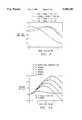
- FIGS. 8-12illustrate the effects on ion flux density for various geometric factors.
- FIG. 8illustrates the effect of antenna geometry on the ion flux distribution at the wafer. Simulations were performed on a 6.5 inch diameter process chamber using an argon plasma at 4 mTorr and an RF power ranging from 200-1500 W. Increasing the overall antenna diameter from 3 in. to 6.5 in. causes the standard deviation to reduce from 40% to 21% over a 150 mm measurement diameter. Further changing the shape of the antenna from planar to contoured, so that the innermost and outermost turns are located 1.5 in, and 0.5 in respectively from the surface of the dielectric capping plate 28, reduces the standard deviation to 17%.
- FIG. 9illustrates the effect of additional antenna geometries on the ion flux distribution at the wafer.
- Enlarging the chamber 10 to 8.75 in., while retaining the antenna diameter at 3 in.has only a minor impact on the uniformity.
- Merely increasing the chamber 10 diameterreduces the standard deviation from 40% to 30%, but simultaneously increasing the antenna diameter to 7 in. reduces the standard deviation to 5%.
- Decreasing the number of turns from 5 to 4has no appreciable effect on the ion flux uniformity. Accordingly, decreasing the number of turns is desirable, since it lowers the inductance of the antenna thus making RF tuning easier.
- Changing the shape of the antenna from planar to contoured, so that the innermost and outermost turns are located 1.5 in, and 0.5 in. respectively from the surface of the dielectric capping plate 28,increases the ion flux at the edge of the wafer relative to the center of the wafer.
- FIG. 10illustrates the effect of the shape of the dielectric capping plate 28 on the ion flux distribution at the wafer.
- the chamber 10 diameteris 12 in. and the gap between the antenna and the wafer is 2 in.
- Contouring the dielectric capping plate 28has the same effect as contouring the antenna 14 (i.e., the ion flux increases at the edge of the wafer relative to the center of the wafer).
- Contouring the dielectric capping plateaffects the plasma distribution in two ways: contouring alters the shape of the plasma generation volume and also affects the electromagnetic field distribution in the plasma. The ability to tailor the ion flux uniformity also allows compensation for gas flow effects. From manufacturing point of view, contouring the dielectric capping plate 28 is easier than contouring the antenna 14.
- FIG. 11illustrates the effect of electrically conducting rings on the ion flux distribution at the wafer. Simulation was performed assuming a planar antenna having five turns and an overall diameter of 7 in. in a chamber 10 of 8.75 in. Electrically conducting rings 50 have a similar effect as contouring the dielectric capping plate. Rings 50 affect the electrostatic and electromagnetic field distribution.
- FIG. 12illustrates the effect of chamber height on the electric field, the ion flux and the ion flux uniformity at the wafer. Simulation was performed based on a planar antenna having 5 turns and an overall diameter of 7 in. in a chamber 10 having a diameter of 8.75 in. Undesirable wafer heating due to the residual electromagnetic fields at the wafer can easily be reduced without substantially altering the ion flux by merely increasing the chamber 10 height slightly. For a given antenna configuration and chamber diameter there is an optimum chamber height for the best ion flux uniformity.
Landscapes
- Physics & Mathematics (AREA)
- Engineering & Computer Science (AREA)
- Plasma & Fusion (AREA)
- Electromagnetism (AREA)
- Spectroscopy & Molecular Physics (AREA)
- Chemical & Material Sciences (AREA)
- Analytical Chemistry (AREA)
- General Physics & Mathematics (AREA)
- Condensed Matter Physics & Semiconductors (AREA)
- Manufacturing & Machinery (AREA)
- Computer Hardware Design (AREA)
- Microelectronics & Electronic Packaging (AREA)
- Power Engineering (AREA)
- Plasma Technology (AREA)
- Drying Of Semiconductors (AREA)
- Chemical Vapour Deposition (AREA)
- ing And Chemical Polishing (AREA)
Abstract
Description
The following related patent application is hereby incorporated by reference:
______________________________________ Ser. No. Filing Date Title ______________________________________ 08/097,498 7/26/93 PLASMA SOURCE AND METHOD OF MANUFACTURING Now U.S. Pat. No. 5,436,528, issued 07/25/95. ______________________________________
This invention relates in general to semiconductor processing equipment and more particularly to an inductively coupled plasma source in a plasma processing chamber.
Inductively coupled plasmas ("CICPs") generated with radio frequency ("RF") waves having a frequency generally between 1 MHz and 100 MHz are capable of providing charged particle (electron and ion) concentrations in excess of 1011 cm-3 and ion currents to wafer substrates in excess of 5 mA/cm2. The ICP source is thus competitive with electron cyclotron resonance ("ECR") plasma sources for plasma processing applications in integrated circuit manufacturing processes. Inductively coupled RF plasma sources have advantages over both capacitively coupled RF plasma sources and ECR plasma sources.
In contrast to capacitive RF coupling, inductively coupled RF plasmas have substantially lower intrinsic plasma potentials (<50 V) and achieve a substantially higher ionization efficiency >5%). Also, the intrinsic plasma potential is relatively independent of the RF power. The low intrinsic plasma potential is useful in applications where high ion energies cannot be tolerated.
As in the case of ECR systems, the ion energy of an inductively coupled RF plasma can be varied independently by biasing the integrated circuit wafer with a separate RF power supply. The ICP source, however, has the advantage of operating over a pressure range that is more compatible with process requirements (1 mTorr to 50 mTorr). An ECR source is most effective at pressures below 10 mTorr. In addition, the ICP source can provide a larger diameter (15 cm to 30 cm), homogeneous plasma, in a compact design, and at substantially lower cost than an ECR source. Since the operating pressure is higher, the pumping requirements for a given gas flow rate are more modest.
A first type of prior plasma source employing RF induction coupling, couples energy into the plasma through whistler or helicon waves. This source is called a helicon plasma source. In the presence of a magnetic field ranging from 100 G to 1 kG directed along the axis of the source, a standing whistler wave can be excited by applying an RF voltage to a loop antenna located around the source cavity. Although these axial magnetic fields are generally weaker than the magnetic fields employed in ECR sources, the plasma is non-uniform across the diameter of the source. Thus, the wafer must be located away or "downstream" of the source, in a region where the plasma is sufficiently uniform. This requires the input power of the source to be increased to maintain a sufficient plasma density (i.e., electron and ion concentration) at the downstream position. Also, large solenoidal coils are required to generate the axial magnetic field. These increase source cost and complexity.
A second type of prior plasma source differs from the generic whistler wave or helicon source by omitting the axial magnetic field. The wafer can therefore be placed within the plasma generation region. Even though the peak plasma densities (5 ×1011 cm-3) for such a some are about an order of magnitude lower than those for the whistler wave source, the proximity of the wafer to the source ensures that processing rates are comparable. Etch rates of over 1 μm/min are possible for many materials of interest. This source is simpler, more compact, and cheaper than the helicon plasma source.
The second type of induction plasma source employs a multi-turn pancake coil located along the top surface of a cylindrical vacuum chamber. A quartz vacuum window, typically 0.5 in. thick, isolates the coil from the chamber. When the coil is powered by an RF source, large currents circulate in the coils. These currents induce intense electric fields inside the chamber that sustain the plasma.
The time-varying magnetic and electric fields generated by a pancake coil are proportional to the coil current, and scale as the square of the number of coil turns. The uniformity of the induced field improves with increasing coil turns. However, the inductance of the coil is proportional to the square of the number of coil turns. This implies that the voltage drop across the coil increases with an increasing number of coil turns for a fixed coil current. As an example, the voltage drop across a 5 μH coil for an RMS current of 20 A at 13.56 MHz is 8.5 kV. Such a high voltage is a hazard and results in capacitive energy coupling between the coil and the plasma. Capacitive coupling is undesirable because the intrinsic plasma potential increases dramatically if a significant amount of energy is transferred via capacitive coupling. These issues constrain the number of coil turns to about three in prior RF plasma sources.
In accordance with the present invention a plasma source and method of manufacture are provided which substantially eliminate or reduce disadvantages and problems associated with prior plasma sources.
A plasma processing structure comprising a plasma processing chamber and an inductively coupled plasma source mounted therein. The inductively coupled plasma source includes a hermetically sealed encapsulated antenna. Various embodiments are disclosed including using a planar or conical antenna, having a dielectric capping plate which may be conical in shape, and adding electrically conducting rings to the surface of a housing that surrounds the antenna. In addition, RF power may be supplied to the antenna through one or more RF matching networks from one or more RF power supplies.
A technical advantage of the invention is providing a method for incorporating an inductively coupled plasma source in a generic plasma processing chamber.
A further advantage of the invention is providing an inductively coupled plasma source having an encapsulated antenna assembly that is hermetically sealed.
A further advantage of the invention is providing an inductively coupled plasma source connected to a plurality of RF tuners and/or generators.
These and other advantages will be apparent to those skilled in the art having reference to the specification in conjunction with drawings.
For a more complete understanding of the present invention, and the advantages thereof, reference is now made to the following descriptions taken in conjunction with the accompanying drawings, in which:
FIG. 1 depicts a partially cross-sectional, partially schematic diagram of a plasma processing chamber employing the disclosed plasma source; and
FIG. 2 illustrates an alternative configuration having a contoured dielectric capping plate adjacent the plasma source;
FIG. 3 illustrates an alternative embodiment plasma source for large area plasmas;
FIG. 4 illustrates an alternative embodiment plasma source having a master-slave link between the RF power supplies for the plasma source and wafer chuck;
FIG. 5 illustrates an alternative configuration of the plasma source having electrically conducting plates on the surface of the antenna housing;
FIG. 6 illustrates an alternative configuration of the plasma source having a contoured antenna;
FIG. 7 illustrates a mechanism for adjusting the spacing between the disclosed plasma source and the wafer chuck;
FIG. 8 is a graph of the effects of antenna geometry on ion flux distribution at the wafer;
FIG. 9 is a graph of the effects of antenna geometry on ion flux distribution at the wafer;
FIG. 10 is a graph of the effects of the shape of the dielectric capping plate on ion flux distribution at the wafer;
FIG. 11 is a graph of the effects of electrically conducting plates on ion flux distribution at the wafer; and
FIG. 12 is a graph of the effects of chamber height on the electric field, ion flux, and the ion flux uniformity at the wafer.
The preferred embodiment of the present invention and its advantages are best understood by referring to FIGS. 1-12 of the drawings, like numerals being used for like and corresponding parts of the various drawings.
FIG. 1 depicts a partially cross-sectional, partially schematic diagram of a genericplasma processing chamber 10 modified to include an inductively coupled plasma (ICP)source 12 according to the invention.ICP source 12 consists of anantenna 14 encapsulated in an epoxy 16 and hermetically sealed inhousing 18.Housing 18 is made of materials that are structurally rigid and resistant to the plasma environment such as ceramics.Epoxy 16 is preferably a general purpose epoxy encapsulant, but any suitable encapsulant may be used. Theantenna 14 typically comprises aluminum tubing and may be segmented with capacitors installed between adjacent segments of aluminum tubing in order to reduce the effective coil impedance as described in detail in U.S. Pat. No. 5,231,334, issued Jul. 27, 1993, assigned to Texas Instruments, Inc. and hereby incorporated by reference.
Still referring to FIG. 1, hermetic sealing of theantenna 14 can be achieved by using a series of O-rings 22 to prevent the epoxy 16 from interacting with the plasma environment. Other methods of hermetic sealing will be apparent to those skilled in the art. Hermetic sealing is desirable since most epoxies are attacked by the highly reactive environment produced by the plasma.
Theentire housing 18 is located within the vacuum environment of theprocess chamber 10 and is preferably bolted to the upper wall of theprocess chamber 10. At least two leads 24 of theantenna 14 penetrate the upper wall of thechamber 10 through insulatingbushings 26. Insulatingbushings 26 preferably comprise a ceramic.Housing 18 may optionally be surrounded by ametal shield 20 if needed to prevent plasma formation behind and around thehousing 18. Also shown in FIG. 1 are other components of ageneric process chamber 10 such aschuck 34 for holdingwafer 36 and the pump outports 38.
Adielectric capping plate 28 separates the surface ofhousing 18 fromplasma formation region 30.Dielectric capping plate 28 may also be made of ceramic. If desired,dielectric capping plate 28 may have a plurality of holes (not shown) so that it may serve as a showerhead for uniform distribution of process gases which may enter theprocess chamber 10 atgas inlet 32. Optimized showerhead hole patterns for uniform gas distribution are well known in the art. The shape ofdielectric capping plate 28 may be contoured to provide better process uniformity. For example,dielectric capping plate 28 may be conical in shape as shown in FIG. 2. Contouring thedielectric capping plate 28 affects the plasma distribution in two ways. First, contouring alters the shape of theplasma formation region 30. Second, contouring changes the electromagnetic field distribution in the plasma and provides the ability to tailor the ion flux uniformity.
Referring back to FIG. 1, theantenna 14 is powered by anRF supply 40 through aRF matching network 42. TheRF matching network 42 may be installed directly over the upper wall of the process chamber as shown in FIG. 1. This will keep the electrical lead lengths between theantenna 14 and thematching network 42 to a minimum. If theprocess chamber 10 has a large diameter, for example, for processing large diameter wafers, several RF matching networks 42a-c may be used as shown in FIG. 3. Having multiple networks 42a-c reduces the impedance to be driven by each network 42a-c. For example, a first RF matching network 42a may be connected to the outermost coils. A secondRF matching network 42b may be connected to the intermediate coils and a thirdRF matching network 42c may be connected to the innermost coils. As shown in FIG. 3, aseparate supply 46,48 (or generator) may be connected to each RF matching network 42a-c. Thesupplies phase shifter 44 between amaster generator 46 and each of theslave generators 48. Thephase shifter 44 is used to adjust the relative phases between thegenerators generator
Referring to FIG. 4, thechuck 34 is typically connected to aRF power supply 54 through amatching network 52. Thechuck 34 andantenna 14 are typically powered by separate RF supplies. When the same RF frequency is desired for both thechuck 34 and theantenna 14, the power supplies need to be operated in a master-slave configuration similar to the one shown in FIG. 3, with thesupply 40 for theantenna 14 serving as the master generator. Avariable phase shifter 56 is inserted in the master-slave link, and the relative phases of the twogenerators
In operation, the desired process gas (or gases) is supplied togas inlet 32. Theantenna 14 is powered by RF power supply 40 (or 46 and 48) to produce large currents that circulate in the coils ofantenna 14. These currents induce intense electric fields inside thechamber 10 inplasma formation region 30. When the process gas supplied throughgas inlet 32 flows through the showerhead holes indielectric capping layer 28 and into the electric field generated by the currents in antenna 14 a plasma is created and sustained. The plasma then reacts with the surface ofwafer 36 in the conventional manner. Becauseantenna 14 is hermetically sealed, the plasma created does not react withepoxy 16. In addition, plasma formation behind and aroundhousing 18 may be prevented if desired by the use ofmetal shield 20.
To further optimize theICP source 12, electricallyconductive plates 50 may be added to the surface ofhousing 18, as shown in FIG. 5.Plates 50 may be electrostatically floating or grounded on the surface ofhousing 18.Plates 50 may comprises aluminum to minimize eddy current heating and losses. Similar to contouringdielectric capping plate 28,plates 50 can be used to tailor the ion flux uniformity at the wafer.Plates 50 may also be used to reduce the electrostatic coupling between the antenna and the plasma by ensuring that there is no electric field directly above theantenna 14. A drawback to usingplates 50 is that some eddy current heating loss occurs.
Several optimizations can be made toantenna 14 to improve process uniformity. For example, the diameter of and number of turns in theantenna 14 may be scaled with wafer diameter and chamber size. Furthermore,antenna 14 may be planar as indicated in FIG. 1 or it may be contoured in order to provide better process uniformity for a particular process chamber. One example of a contoured antenna is theconical antenna 14 shown in FIG. 6. As shown in FIG. 6, the innermost turns ofantenna 14 are further away from thechuck 34 than the outermost turns.
If desired, the spacing between thewafer 36 and thehousing 18 can be designed to be adjustable. Accordingly, the spacing between thewafer 36 and thehousing 18 could be adjusted to optimize process uniformity and minimizewafer 36 heating due to electromagnetic fields. For example, the spacing may be varied by incorporatingspacers 58 between theICP 12 and the upper wall of theprocess chamber 10, as shown in FIG. 7. In addition, a set ofmulti-polar magnets 60 around the periphery ofprocess chamber 10 may be provided to generate a multipolar magnetic field to improve plasma confinement and extend operation to lower pressures.
Another optimization technique involves operating theICP source 12 in a time-modulated power mode in which the input RF power to theantenna 14 is time modulated. For example, a square wave modulation of the power may be used. Time modulation is useful for optimizing the mix of species in the plasma discharge. Time modulation has been shown to be beneficial for reactive ion etching and electron cyclotron resonance etching systems.
FIGS. 8-12 illustrate the effects on ion flux density for various geometric factors. FIG. 8 illustrates the effect of antenna geometry on the ion flux distribution at the wafer. Simulations were performed on a 6.5 inch diameter process chamber using an argon plasma at 4 mTorr and an RF power ranging from 200-1500 W. Increasing the overall antenna diameter from 3 in. to 6.5 in. causes the standard deviation to reduce from 40% to 21% over a 150 mm measurement diameter. Further changing the shape of the antenna from planar to contoured, so that the innermost and outermost turns are located 1.5 in, and 0.5 in respectively from the surface of thedielectric capping plate 28, reduces the standard deviation to 17%.
FIG. 9 illustrates the effect of additional antenna geometries on the ion flux distribution at the wafer. Enlarging thechamber 10 to 8.75 in., while retaining the antenna diameter at 3 in. has only a minor impact on the uniformity. Merely increasing thechamber 10 diameter reduces the standard deviation from 40% to 30%, but simultaneously increasing the antenna diameter to 7 in. reduces the standard deviation to 5%. Decreasing the number of turns from 5 to 4 has no appreciable effect on the ion flux uniformity. Accordingly, decreasing the number of turns is desirable, since it lowers the inductance of the antenna thus making RF tuning easier. Changing the shape of the antenna from planar to contoured, so that the innermost and outermost turns are located 1.5 in, and 0.5 in. respectively from the surface of thedielectric capping plate 28, increases the ion flux at the edge of the wafer relative to the center of the wafer.
FIG. 10 illustrates the effect of the shape of thedielectric capping plate 28 on the ion flux distribution at the wafer. Thechamber 10 diameter is 12 in. and the gap between the antenna and the wafer is 2 in. Contouring thedielectric capping plate 28 has the same effect as contouring the antenna 14 (i.e., the ion flux increases at the edge of the wafer relative to the center of the wafer). Contouring the dielectric capping plate affects the plasma distribution in two ways: contouring alters the shape of the plasma generation volume and also affects the electromagnetic field distribution in the plasma. The ability to tailor the ion flux uniformity also allows compensation for gas flow effects. From manufacturing point of view, contouring thedielectric capping plate 28 is easier than contouring theantenna 14.
FIG. 11 illustrates the effect of electrically conducting rings on the ion flux distribution at the wafer. Simulation was performed assuming a planar antenna having five turns and an overall diameter of 7 in. in achamber 10 of 8.75 in. Electrically conducting rings 50 have a similar effect as contouring the dielectric capping plate.Rings 50 affect the electrostatic and electromagnetic field distribution.
FIG. 12 illustrates the effect of chamber height on the electric field, the ion flux and the ion flux uniformity at the wafer. Simulation was performed based on a planar antenna having 5 turns and an overall diameter of 7 in. in achamber 10 having a diameter of 8.75 in. Undesirable wafer heating due to the residual electromagnetic fields at the wafer can easily be reduced without substantially altering the ion flux by merely increasing thechamber 10 height slightly. For a given antenna configuration and chamber diameter there is an optimum chamber height for the best ion flux uniformity.
Although the present invention and its advantages have been described in detail, it should be understood that various changes, substitutions and alterations can be made herein without departing from the spirit and scope of the invention as defined by the appended claims.
Claims (28)
1. A plasma processing structure comprising:
a processing chamber;
an inductively coupled plasma source mounted within said processing chamber, said inductively coupled plasma source comprising an antenna encapsulated in an encapsulant, wherein said antenna and said encapsulant are hermetically sealed.
2. The structure of claim 1, further comprising a structurally rigid housing surrounding said encapsulated antenna.
3. The structure of claim 2, further comprising a conductive shield surrounding said housing except on a first side to prevent plasma formation behind and laterally adjacent said housing.
4. The structure of claim 2, further comprising at least one electrically conductive plate located on a side of said housing.
5. The structure of claim 1, wherein said antenna is planar.
6. The structure of claim 1, wherein said antenna is contoured.
7. The structure of claim 1, further comprising a dielectric capping plate of a side of said encapsulated antenna.
8. The structure of claim 7, wherein said dielectric capping plate is contoured.
9. The structure of claim 1, further comprising one or more matching networks connected to said encapsulated antenna and one or more RF power supplies connected to said matching networks for supplying RF power to said encapsulated antenna.
10. The structure of claim 9, wherein said at least one RF power supply comprises a master power supply and at least one slave power supply connected in a master-slave configuration having a phase shifter located between said master power supply and said at least one slave power supply.
11. The structure of claim 1, further comprising:
a chuck for holding a wafer located within said processing chamber;
a first RF power supply connected to said chuck through a matching network; and
a phase shifter connected between said first RF power supply for said chuck and a second RF power supply connected to said antenna.
12. The structure of claim 1, further comprising a plurality of multi-polar magnets located on a sidewall of said processing chamber.
13. The structure of claim 1, wherein said antenna comprises a plurality of coil segments separated from each other by a capacitor and an insulator.
14. A plasma processing chamber comprising:
an inductively coupled plasma source attached to an internal wall of said plasma processing chamber, said inductively coupled plasma source comprising:
a spiral antenna encapsulated in epoxy;
a structurally rigid housing surrounding the epoxy, wherein said epoxy and antenna are hermetically sealed; and
a dielectric capping plate having a plurality of holes, said dielectric capping plate being located adjacent a first side of said housing.
15. The plasma processing chamber of claim 14, wherein said spiral antenna comprises a plurality of leads extending through said internal wall of said plasma processing chamber.
16. The plasma processing chamber of claim 15, further comprising at least one matching network connected to said plurality of leads and at least one RF power supply connected to said at least one matching network for supplying RF power to said spiral antenna.
17. The plasma processing chamber of claim 16, wherein said at least one RF power supply comprises a master power supply and one or more slave power supplies connected in a master-slave configuration having a phase shifter located between said master power supply and said one or more slave power supplies.
18. The plasma processing chamber of claim 14, wherein said dielectric capping plate is contoured.
19. The plasma processing chamber of claim 14, wherein said antenna is contoured.
20. The plasma processing chamber of claim 14, further comprising at least one electrically conducting ring located on said first side of said housing.
21. The plasma processing chamber of claim 14, wherein said antenna comprises a plurality of coil segments separated from each other by a capacitor and an insulator.
22. A method for incorporating an inductively coupled plasma source in a plasma processing chamber comprising the steps of:
providing a plasma processing chamber having a chuck for holding a wafer;
encapsulating a spiral antenna in an epoxy;
surrounding said antenna and epoxy with a structurally rigid housing;
hermetically sealing said epoxy;
attaching said housing to an internal wall of said plasma processing chamber; and
providing a dielectric capping plate to a first side of said housing.
23. The method of claim 22, further comprising the steps of
supplying RF power to said spiral antenna; and
providing at least one process gas to said plasma processing chamber to form a plasma.
24. The method of claim 23, further comprising the step of time modulating the RF power supplied to said spiral antenna.
25. The method of claim 22, further comprising the step of placing spacers between said housing and said internal wall to adjust the spacing between said housing and said chuck.
26. The method of claim 22, further comprising the step of contouring said dielectric capping plate.
27. The method of claim 22, further comprising the step of contouring said spiral antenna into a conical shape.
28. The method of claim 22, further comprising the step of placing electrically conductive plates on said first side of said housing.
Priority Applications (7)
| Application Number | Priority Date | Filing Date | Title |
|---|---|---|---|
| US08/269,414US5580385A (en) | 1994-06-30 | 1994-06-30 | Structure and method for incorporating an inductively coupled plasma source in a plasma processing chamber |
| US08/472,606US5591493A (en) | 1994-06-30 | 1995-06-07 | Structure and method for incorporating an inductively coupled plasma source in a plasma processing chamber |
| KR1019950017440AKR100373815B1 (en) | 1994-06-30 | 1995-06-26 | Apparatus and method for coupling inductively coupled plasma sources to a plasma processing chamber |
| EP95110150AEP0690666B1 (en) | 1994-06-30 | 1995-06-29 | Structure and method for semiconductor processing |
| DE69504254TDE69504254T2 (en) | 1994-06-30 | 1995-06-29 | Semiconductor processing apparatus and method |
| JP7166511AJPH08195297A (en) | 1994-06-30 | 1995-06-30 | Structure and method of incorporating inductively connected plasma source into plasma processing box |
| TW090212272UTW501842U (en) | 1994-06-30 | 1995-12-27 | Structure for incorporationg an inductively coupled plasma source in plasma processing chamber |
Applications Claiming Priority (1)
| Application Number | Priority Date | Filing Date | Title |
|---|---|---|---|
| US08/269,414US5580385A (en) | 1994-06-30 | 1994-06-30 | Structure and method for incorporating an inductively coupled plasma source in a plasma processing chamber |
Related Child Applications (1)
| Application Number | Title | Priority Date | Filing Date |
|---|---|---|---|
| US08/472,606DivisionUS5591493A (en) | 1994-06-30 | 1995-06-07 | Structure and method for incorporating an inductively coupled plasma source in a plasma processing chamber |
Publications (1)
| Publication Number | Publication Date |
|---|---|
| US5580385Atrue US5580385A (en) | 1996-12-03 |
Family
ID=23027137
Family Applications (2)
| Application Number | Title | Priority Date | Filing Date |
|---|---|---|---|
| US08/269,414Expired - LifetimeUS5580385A (en) | 1994-06-30 | 1994-06-30 | Structure and method for incorporating an inductively coupled plasma source in a plasma processing chamber |
| US08/472,606Expired - LifetimeUS5591493A (en) | 1994-06-30 | 1995-06-07 | Structure and method for incorporating an inductively coupled plasma source in a plasma processing chamber |
Family Applications After (1)
| Application Number | Title | Priority Date | Filing Date |
|---|---|---|---|
| US08/472,606Expired - LifetimeUS5591493A (en) | 1994-06-30 | 1995-06-07 | Structure and method for incorporating an inductively coupled plasma source in a plasma processing chamber |
Country Status (6)
| Country | Link |
|---|---|
| US (2) | US5580385A (en) |
| EP (1) | EP0690666B1 (en) |
| JP (1) | JPH08195297A (en) |
| KR (1) | KR100373815B1 (en) |
| DE (1) | DE69504254T2 (en) |
| TW (1) | TW501842U (en) |
Cited By (106)
| Publication number | Priority date | Publication date | Assignee | Title |
|---|---|---|---|---|
| US5792261A (en)* | 1993-12-17 | 1998-08-11 | Tokyo Electron Limited | Plasma process apparatus |
| US5824605A (en)* | 1995-07-31 | 1998-10-20 | Lam Research Corporation | Gas dispersion window for plasma apparatus and method of use thereof |
| US5863376A (en)* | 1996-06-05 | 1999-01-26 | Lam Research Corporation | Temperature controlling method and apparatus for a plasma processing chamber |
| US5993594A (en)* | 1996-09-30 | 1999-11-30 | Lam Research Corporation | Particle controlling method and apparatus for a plasma processing chamber |
| US6033585A (en)* | 1996-12-20 | 2000-03-07 | Lam Research Corporation | Method and apparatus for preventing lightup of gas distribution holes |
| US6035868A (en)* | 1997-03-31 | 2000-03-14 | Lam Research Corporation | Method and apparatus for control of deposit build-up on an inner surface of a plasma processing chamber |
| US6043608A (en)* | 1996-10-31 | 2000-03-28 | Nec Corporation | Plasma processing apparatus |
| US6048798A (en)* | 1996-06-05 | 2000-04-11 | Lam Research Corporation | Apparatus for reducing process drift in inductive coupled plasma etching such as oxide layer |
| US6079357A (en)* | 1997-10-21 | 2000-06-27 | Tokyo Electron Yamanashi Limited | Plasma processing apparatus |
| US6089182A (en)* | 1995-08-17 | 2000-07-18 | Tokyo Electron Limited | Plasma processing apparatus |
| US6155199A (en)* | 1998-03-31 | 2000-12-05 | Lam Research Corporation | Parallel-antenna transformer-coupled plasma generation system |
| US6164241A (en)* | 1998-06-30 | 2000-12-26 | Lam Research Corporation | Multiple coil antenna for inductively-coupled plasma generation systems |
| US6189484B1 (en)* | 1999-03-05 | 2001-02-20 | Applied Materials Inc. | Plasma reactor having a helicon wave high density plasma source |
| US6203620B1 (en)* | 1996-07-10 | 2001-03-20 | Cvc Products Inc | Hermetically-sealed inductively-coupled plasma source structure and method of use |
| US6230651B1 (en) | 1998-12-30 | 2001-05-15 | Lam Research Corporation | Gas injection system for plasma processing |
| US6237526B1 (en) | 1999-03-26 | 2001-05-29 | Tokyo Electron Limited | Process apparatus and method for improving plasma distribution and performance in an inductively coupled plasma |
| DE19955671A1 (en)* | 1999-11-19 | 2001-05-31 | Muegge Electronic Gmbh | Device for generating plasma in treatment chamber has dividing plate between treatment chamber, antenna chamber in which plasma is not generated owing to higher pressure/gas filling |
| US6245202B1 (en)* | 1996-04-12 | 2001-06-12 | Hitachi, Ltd. | Plasma treatment device |
| RU2171555C1 (en)* | 2000-03-06 | 2001-07-27 | Берлин Евгений Владимирович | High-frequency gaseous-discharge source of high-density ions with low-impedance antenna |
| US6440220B1 (en)* | 1998-10-23 | 2002-08-27 | Goodrich Corporation | Method and apparatus for inhibiting infiltration of a reactive gas into porous refractory insulation |
| US6474258B2 (en) | 1999-03-26 | 2002-11-05 | Tokyo Electron Limited | Apparatus and method for improving plasma distribution and performance in an inductively coupled plasma |
| US6494998B1 (en) | 2000-08-30 | 2002-12-17 | Tokyo Electron Limited | Process apparatus and method for improving plasma distribution and performance in an inductively coupled plasma using an internal inductive element |
| US20020189763A1 (en)* | 2001-06-19 | 2002-12-19 | Jusung Engineering Co., Ltd. | Plasma processing apparatus having parallel resonance antenna for very high frequency |
| US20030150710A1 (en)* | 2001-10-09 | 2003-08-14 | Evans John D. | Plasma production device and method and RF driver circuit |
| US20040004220A1 (en)* | 2002-06-21 | 2004-01-08 | Koji Suzuki | Thin film transistor |
| US20040026231A1 (en)* | 2001-10-09 | 2004-02-12 | Pribyl Patrick A. | Plasma production device and method and RF driver circuit with adjustable duty cycle |
| US6805952B2 (en) | 2000-12-29 | 2004-10-19 | Lam Research Corporation | Low contamination plasma chamber components and methods for making the same |
| US20040263412A1 (en)* | 2001-10-09 | 2004-12-30 | Patrick Pribyl | Plasma production device and method and RF driver circuit with adjustable duty cycle |
| US6929830B2 (en) | 1997-12-12 | 2005-08-16 | Canon Kabushiki Kaisha | Plasma treatment method and method of manufacturing optical parts using the same |
| US20060137611A1 (en)* | 2004-12-24 | 2006-06-29 | Samsung Electronics Co., Ltd. | Plasma apparatus |
| US20070235327A1 (en)* | 2006-03-31 | 2007-10-11 | Tokyo Electron Limited | Internal coil with segmented shield and inductively-coupled plasma source and processing system therewith |
| US20070251451A1 (en)* | 2001-09-10 | 2007-11-01 | Tegal Corporation | Nanolayer Thick Film Processing System |
| US20080168945A1 (en)* | 2007-01-15 | 2008-07-17 | Hong-Seub Kim | Plasma generating apparatus |
| US20100041238A1 (en)* | 2001-10-15 | 2010-02-18 | Lam Research Corporation | Tunable multi-zone gas injection system |
| US20100190353A1 (en)* | 2003-02-04 | 2010-07-29 | Tegal Corporation | Nanolayer deposition process |
| US20100224321A1 (en)* | 2009-03-05 | 2010-09-09 | Applied Materials, Inc. | Inductively coupled plasma reactor having rf phase control and methods of use thereof |
| US20100285237A1 (en)* | 2001-09-10 | 2010-11-11 | Tegal Corporation | Nanolayer deposition using bias power treatment |
| CN1881537B (en)* | 1999-07-22 | 2011-04-20 | 株式会社半导体能源研究所 | Method for manufacturing active matrix display |
| WO2013162419A2 (en) | 2012-04-24 | 2013-10-31 | Berlin Evgenij Vladimirovich | Plasma generator (variants) |
| CN103715052A (en)* | 2012-10-09 | 2014-04-09 | 诺发系统公司 | Hybrid Impedance Matching for Inductively Coupled Plasma Systems |
| US9121098B2 (en) | 2003-02-04 | 2015-09-01 | Asm International N.V. | NanoLayer Deposition process for composite films |
| US20180308668A1 (en)* | 2017-02-15 | 2018-10-25 | Yield Engineering Systems, Inc. | Plasma Spreading Apparatus And Method Of Spreading Plasma In Process Ovens |
| US20190198291A1 (en)* | 2016-10-04 | 2019-06-27 | Applied Materials, Inc. | Chamber with flow-through source |
| US10468267B2 (en) | 2017-05-31 | 2019-11-05 | Applied Materials, Inc. | Water-free etching methods |
| US10490418B2 (en) | 2014-10-14 | 2019-11-26 | Applied Materials, Inc. | Systems and methods for internal surface conditioning assessment in plasma processing equipment |
| US10490406B2 (en) | 2018-04-10 | 2019-11-26 | Appled Materials, Inc. | Systems and methods for material breakthrough |
| US10497573B2 (en) | 2018-03-13 | 2019-12-03 | Applied Materials, Inc. | Selective atomic layer etching of semiconductor materials |
| US10504754B2 (en) | 2016-05-19 | 2019-12-10 | Applied Materials, Inc. | Systems and methods for improved semiconductor etching and component protection |
| US10522371B2 (en) | 2016-05-19 | 2019-12-31 | Applied Materials, Inc. | Systems and methods for improved semiconductor etching and component protection |
| US10529737B2 (en) | 2017-02-08 | 2020-01-07 | Applied Materials, Inc. | Accommodating imperfectly aligned memory holes |
| US10541184B2 (en) | 2017-07-11 | 2020-01-21 | Applied Materials, Inc. | Optical emission spectroscopic techniques for monitoring etching |
| US10541246B2 (en) | 2017-06-26 | 2020-01-21 | Applied Materials, Inc. | 3D flash memory cells which discourage cross-cell electrical tunneling |
| US10546729B2 (en) | 2016-10-04 | 2020-01-28 | Applied Materials, Inc. | Dual-channel showerhead with improved profile |
| US10573496B2 (en) | 2014-12-09 | 2020-02-25 | Applied Materials, Inc. | Direct outlet toroidal plasma source |
| US10573527B2 (en) | 2018-04-06 | 2020-02-25 | Applied Materials, Inc. | Gas-phase selective etching systems and methods |
| US10593553B2 (en) | 2017-08-04 | 2020-03-17 | Applied Materials, Inc. | Germanium etching systems and methods |
| US10593560B2 (en) | 2018-03-01 | 2020-03-17 | Applied Materials, Inc. | Magnetic induction plasma source for semiconductor processes and equipment |
| US10593523B2 (en) | 2014-10-14 | 2020-03-17 | Applied Materials, Inc. | Systems and methods for internal surface conditioning in plasma processing equipment |
| US10600639B2 (en) | 2016-11-14 | 2020-03-24 | Applied Materials, Inc. | SiN spacer profile patterning |
| US10607867B2 (en) | 2015-08-06 | 2020-03-31 | Applied Materials, Inc. | Bolted wafer chuck thermal management systems and methods for wafer processing systems |
| US10615047B2 (en) | 2018-02-28 | 2020-04-07 | Applied Materials, Inc. | Systems and methods to form airgaps |
| US10629473B2 (en) | 2016-09-09 | 2020-04-21 | Applied Materials, Inc. | Footing removal for nitride spacer |
| US10672642B2 (en) | 2018-07-24 | 2020-06-02 | Applied Materials, Inc. | Systems and methods for pedestal configuration |
| US10679870B2 (en) | 2018-02-15 | 2020-06-09 | Applied Materials, Inc. | Semiconductor processing chamber multistage mixing apparatus |
| US10699879B2 (en) | 2018-04-17 | 2020-06-30 | Applied Materials, Inc. | Two piece electrode assembly with gap for plasma control |
| US10727080B2 (en) | 2017-07-07 | 2020-07-28 | Applied Materials, Inc. | Tantalum-containing material removal |
| US10755941B2 (en) | 2018-07-06 | 2020-08-25 | Applied Materials, Inc. | Self-limiting selective etching systems and methods |
| US10770346B2 (en) | 2016-11-11 | 2020-09-08 | Applied Materials, Inc. | Selective cobalt removal for bottom up gapfill |
| US10854426B2 (en) | 2018-01-08 | 2020-12-01 | Applied Materials, Inc. | Metal recess for semiconductor structures |
| US10872778B2 (en) | 2018-07-06 | 2020-12-22 | Applied Materials, Inc. | Systems and methods utilizing solid-phase etchants |
| US10886137B2 (en) | 2018-04-30 | 2021-01-05 | Applied Materials, Inc. | Selective nitride removal |
| US10892198B2 (en) | 2018-09-14 | 2021-01-12 | Applied Materials, Inc. | Systems and methods for improved performance in semiconductor processing |
| US10903054B2 (en) | 2017-12-19 | 2021-01-26 | Applied Materials, Inc. | Multi-zone gas distribution systems and methods |
| US10903052B2 (en) | 2017-02-03 | 2021-01-26 | Applied Materials, Inc. | Systems and methods for radial and azimuthal control of plasma uniformity |
| US10920319B2 (en) | 2019-01-11 | 2021-02-16 | Applied Materials, Inc. | Ceramic showerheads with conductive electrodes |
| US10920320B2 (en) | 2017-06-16 | 2021-02-16 | Applied Materials, Inc. | Plasma health determination in semiconductor substrate processing reactors |
| US10943834B2 (en) | 2017-03-13 | 2021-03-09 | Applied Materials, Inc. | Replacement contact process |
| US10964512B2 (en) | 2018-02-15 | 2021-03-30 | Applied Materials, Inc. | Semiconductor processing chamber multistage mixing apparatus and methods |
| US11004689B2 (en) | 2018-03-12 | 2021-05-11 | Applied Materials, Inc. | Thermal silicon etch |
| US11024486B2 (en) | 2013-02-08 | 2021-06-01 | Applied Materials, Inc. | Semiconductor processing systems having multiple plasma configurations |
| US11049755B2 (en) | 2018-09-14 | 2021-06-29 | Applied Materials, Inc. | Semiconductor substrate supports with embedded RF shield |
| US11062887B2 (en) | 2018-09-17 | 2021-07-13 | Applied Materials, Inc. | High temperature RF heater pedestals |
| US11094508B2 (en)* | 2018-12-14 | 2021-08-17 | Applied Materials, Inc. | Film stress control for plasma enhanced chemical vapor deposition |
| US11101136B2 (en) | 2017-08-07 | 2021-08-24 | Applied Materials, Inc. | Process window widening using coated parts in plasma etch processes |
| US11121002B2 (en) | 2018-10-24 | 2021-09-14 | Applied Materials, Inc. | Systems and methods for etching metals and metal derivatives |
| US11158527B2 (en) | 2015-08-06 | 2021-10-26 | Applied Materials, Inc. | Thermal management systems and methods for wafer processing systems |
| US11239061B2 (en) | 2014-11-26 | 2022-02-01 | Applied Materials, Inc. | Methods and systems to enhance process uniformity |
| US11264213B2 (en) | 2012-09-21 | 2022-03-01 | Applied Materials, Inc. | Chemical control features in wafer process equipment |
| US11276590B2 (en) | 2017-05-17 | 2022-03-15 | Applied Materials, Inc. | Multi-zone semiconductor substrate supports |
| US11276559B2 (en) | 2017-05-17 | 2022-03-15 | Applied Materials, Inc. | Semiconductor processing chamber for multiple precursor flow |
| US11309167B2 (en)* | 2018-06-25 | 2022-04-19 | Toshiba Mitsubishi-Electric Industrial Systems Corporation | Active gas generation apparatus and deposition processing apparatus |
| US11328909B2 (en) | 2017-12-22 | 2022-05-10 | Applied Materials, Inc. | Chamber conditioning and removal processes |
| US11417534B2 (en) | 2018-09-21 | 2022-08-16 | Applied Materials, Inc. | Selective material removal |
| US11437242B2 (en) | 2018-11-27 | 2022-09-06 | Applied Materials, Inc. | Selective removal of silicon-containing materials |
| US11476093B2 (en) | 2015-08-27 | 2022-10-18 | Applied Materials, Inc. | Plasma etching systems and methods with secondary plasma injection |
| US11594428B2 (en) | 2015-02-03 | 2023-02-28 | Applied Materials, Inc. | Low temperature chuck for plasma processing systems |
| US11682560B2 (en) | 2018-10-11 | 2023-06-20 | Applied Materials, Inc. | Systems and methods for hafnium-containing film removal |
| US11721527B2 (en) | 2019-01-07 | 2023-08-08 | Applied Materials, Inc. | Processing chamber mixing systems |
| US11984298B2 (en) | 2019-12-02 | 2024-05-14 | Lam Research Corporation | Impedance transformation in radio-frequency-assisted plasma generation |
| US11994542B2 (en) | 2020-03-27 | 2024-05-28 | Lam Research Corporation | RF signal parameter measurement in an integrated circuit fabrication chamber |
| US12057329B2 (en) | 2016-06-29 | 2024-08-06 | Applied Materials, Inc. | Selective etch using material modification and RF pulsing |
| US12136938B2 (en) | 2019-05-07 | 2024-11-05 | Lam Research Corporation | Closed-loop multiple-output radio frequency (RF) matching |
| US12205796B2 (en) | 2019-07-31 | 2025-01-21 | Lam Research Corporation | Radio frequency power generator having multiple output ports |
| US12283462B2 (en) | 2020-06-12 | 2025-04-22 | Lam Research Corporation | Control of plasma formation by RF coupling structures |
| US12340979B2 (en) | 2017-05-17 | 2025-06-24 | Applied Materials, Inc. | Semiconductor processing chamber for improved precursor flow |
| US12394594B2 (en) | 2016-11-03 | 2025-08-19 | En2core Technology Inc. | Inductive coil structure and inductively coupled plasma generation system |
Families Citing this family (39)
| Publication number | Priority date | Publication date | Assignee | Title |
|---|---|---|---|---|
| JP3257328B2 (en)* | 1995-03-16 | 2002-02-18 | 株式会社日立製作所 | Plasma processing apparatus and plasma processing method |
| US20050236109A1 (en)* | 1995-03-16 | 2005-10-27 | Toshio Masuda | Plasma etching apparatus and plasma etching method |
| US5716451A (en)* | 1995-08-17 | 1998-02-10 | Tokyo Electron Limited | Plasma processing apparatus |
| US5965034A (en)* | 1995-12-04 | 1999-10-12 | Mc Electronics Co., Ltd. | High frequency plasma process wherein the plasma is executed by an inductive structure in which the phase and anti-phase portion of the capacitive currents between the inductive structure and the plasma are balanced |
| EP0805475B1 (en)* | 1996-05-02 | 2003-02-19 | Tokyo Electron Limited | Plasma processing apparatus |
| US5897712A (en)* | 1996-07-16 | 1999-04-27 | Applied Materials, Inc. | Plasma uniformity control for an inductive plasma source |
| KR100505176B1 (en) | 1996-09-27 | 2005-10-10 | 서페이스 테크놀로지 시스템스 피엘씨 | Plasma Processing Equipment |
| US6534922B2 (en) | 1996-09-27 | 2003-03-18 | Surface Technology Systems, Plc | Plasma processing apparatus |
| US6308654B1 (en)* | 1996-10-18 | 2001-10-30 | Applied Materials, Inc. | Inductively coupled parallel-plate plasma reactor with a conical dome |
| US6579426B1 (en) | 1997-05-16 | 2003-06-17 | Applied Materials, Inc. | Use of variable impedance to control coil sputter distribution |
| US6652717B1 (en) | 1997-05-16 | 2003-11-25 | Applied Materials, Inc. | Use of variable impedance to control coil sputter distribution |
| US6178920B1 (en) | 1997-06-05 | 2001-01-30 | Applied Materials, Inc. | Plasma reactor with internal inductive antenna capable of generating helicon wave |
| US6071372A (en)* | 1997-06-05 | 2000-06-06 | Applied Materials, Inc. | RF plasma etch reactor with internal inductive coil antenna and electrically conductive chamber walls |
| US6158384A (en)* | 1997-06-05 | 2000-12-12 | Applied Materials, Inc. | Plasma reactor with multiple small internal inductive antennas |
| US6235169B1 (en) | 1997-08-07 | 2001-05-22 | Applied Materials, Inc. | Modulated power for ionized metal plasma deposition |
| US6345588B1 (en) | 1997-08-07 | 2002-02-12 | Applied Materials, Inc. | Use of variable RF generator to control coil voltage distribution |
| JPH11135438A (en)* | 1997-10-28 | 1999-05-21 | Nippon Asm Kk | Semiconductor plasma processing apparatus |
| US6136165A (en)* | 1997-11-26 | 2000-10-24 | Cvc Products, Inc. | Apparatus for inductively-coupled-plasma-enhanced ionized physical-vapor deposition |
| US6254738B1 (en) | 1998-03-31 | 2001-07-03 | Applied Materials, Inc. | Use of variable impedance having rotating core to control coil sputter distribution |
| US5998933A (en)* | 1998-04-06 | 1999-12-07 | Shun'ko; Evgeny V. | RF plasma inductor with closed ferrite core |
| TW434636B (en) | 1998-07-13 | 2001-05-16 | Applied Komatsu Technology Inc | RF matching network with distributed outputs |
| EP1147544A2 (en)* | 1998-09-22 | 2001-10-24 | Applied Materials, Inc. | Rf plasma etch reactor with internal inductive coil antenna and electrically conductive chamber walls |
| US6418874B1 (en) | 2000-05-25 | 2002-07-16 | Applied Materials, Inc. | Toroidal plasma source for plasma processing |
| US6632322B1 (en)* | 2000-06-30 | 2003-10-14 | Lam Research Corporation | Switched uniformity control |
| US6471830B1 (en) | 2000-10-03 | 2002-10-29 | Veeco/Cvc, Inc. | Inductively-coupled-plasma ionized physical-vapor deposition apparatus, method and system |
| US6634313B2 (en) | 2001-02-13 | 2003-10-21 | Applied Materials, Inc. | High-frequency electrostatically shielded toroidal plasma and radical source |
| US6755150B2 (en)* | 2001-04-20 | 2004-06-29 | Applied Materials Inc. | Multi-core transformer plasma source |
| DE10308539B3 (en)* | 2003-02-27 | 2004-06-03 | Bauer Maschinen Gmbh | Cutting device for cutting grooves in the ground comprises cutting elements arranged on the cutting wheels to remove soil using a rotary action |
| US20040237897A1 (en)* | 2003-05-27 | 2004-12-02 | Hiroji Hanawa | High-Frequency electrostatically shielded toroidal plasma and radical source |
| EP1729551A4 (en)* | 2004-03-26 | 2009-08-12 | Nissin Electric Co Ltd | Plasma generating equipment |
| KR100721573B1 (en) | 2005-01-20 | 2007-05-23 | 삼성에스디아이 주식회사 | Inductively Coupled Plasma Treatment System |
| KR100721572B1 (en) | 2005-01-20 | 2007-05-23 | 삼성에스디아이 주식회사 | Inductively Coupled Plasma Treatment System |
| CN100372075C (en)* | 2005-04-15 | 2008-02-27 | 北京北方微电子基地设备工艺研究中心有限责任公司 | An inductively coupled plasma device |
| KR101313705B1 (en)* | 2005-06-24 | 2013-10-01 | 주성엔지니어링(주) | Deposition method of low temperature poly silicon and plasma generation apparatus for the same |
| JP5215685B2 (en)* | 2008-02-14 | 2013-06-19 | 三井造船株式会社 | Atomic layer growth equipment |
| US20110278260A1 (en) | 2010-05-14 | 2011-11-17 | Applied Materials, Inc. | Inductive plasma source with metallic shower head using b-field concentrator |
| US20140288850A1 (en)* | 2011-10-30 | 2014-09-25 | Paskal Technologies Agriculture Cooperative LTD. | Self-learning of plant growth strategy in a greenhouse |
| KR101826883B1 (en)* | 2016-11-03 | 2018-02-08 | 인투코어테크놀로지 주식회사 | Inductive Coil Structure And Inductively Coupled Plasma Apparatus |
| JP2025136978A (en)* | 2024-03-08 | 2025-09-19 | 東京エレクトロン株式会社 | Plasma processing apparatus and plasma processing method |
Citations (9)
| Publication number | Priority date | Publication date | Assignee | Title |
|---|---|---|---|---|
| US4361114A (en)* | 1980-10-06 | 1982-11-30 | Optical Coating Laboratory, Inc. | Method and apparatus for forming thin film oxide layers using reactive evaporation techniques |
| US4948458A (en)* | 1989-08-14 | 1990-08-14 | Lam Research Corporation | Method and apparatus for producing magnetically-coupled planar plasma |
| US5036252A (en)* | 1988-04-26 | 1991-07-30 | Hauzer Holding Bv | Radio frequency ion beam source |
| EP0467046A2 (en)* | 1990-07-17 | 1992-01-22 | Balzers Aktiengesellschaft | Device for etching or crating |
| US5231334A (en)* | 1992-04-15 | 1993-07-27 | Texas Instruments Incorporated | Plasma source and method of manufacturing |
| EP0601468A1 (en)* | 1992-12-01 | 1994-06-15 | Applied Materials, Inc. | Process and electromagnetically coupled planar plasma apparatus for etching oxides |
| US5346578A (en)* | 1992-11-04 | 1994-09-13 | Novellus Systems, Inc. | Induction plasma source |
| US5439524A (en)* | 1993-04-05 | 1995-08-08 | Vlsi Technology, Inc. | Plasma processing apparatus |
| US5464476A (en)* | 1993-10-19 | 1995-11-07 | Central Research Laboratories Limited | Plasma processing device comprising plural RF inductive coils |
Family Cites Families (6)
| Publication number | Priority date | Publication date | Assignee | Title |
|---|---|---|---|---|
| US4675690A (en)* | 1984-05-25 | 1987-06-23 | Revlon, Inc. | Conical spiral antenna |
| JPS62133724A (en)* | 1985-12-06 | 1987-06-16 | Toshiba Corp | Method for manufacturing bias sputter thin film |
| GB8905075D0 (en)* | 1989-03-06 | 1989-04-19 | Nordiko Ltd | Electrode assembly and apparatus |
| US5200595A (en)* | 1991-04-12 | 1993-04-06 | Universite De Sherbrooke | High performance induction plasma torch with a water-cooled ceramic confinement tube |
| US5244730A (en)* | 1991-04-30 | 1993-09-14 | International Business Machines Corporation | Plasma deposition of fluorocarbon |
| US5260236A (en)* | 1991-06-07 | 1993-11-09 | Intel Corporation | UV transparent oxynitride deposition in single wafer PECVD system |
- 1994
- 1994-06-30USUS08/269,414patent/US5580385A/ennot_activeExpired - Lifetime
- 1995
- 1995-06-07USUS08/472,606patent/US5591493A/ennot_activeExpired - Lifetime
- 1995-06-26KRKR1019950017440Apatent/KR100373815B1/ennot_activeExpired - Fee Related
- 1995-06-29DEDE69504254Tpatent/DE69504254T2/ennot_activeExpired - Fee Related
- 1995-06-29EPEP95110150Apatent/EP0690666B1/ennot_activeExpired - Lifetime
- 1995-06-30JPJP7166511Apatent/JPH08195297A/enactivePending
- 1995-12-27TWTW090212272Upatent/TW501842U/ennot_activeIP Right Cessation
Patent Citations (12)
| Publication number | Priority date | Publication date | Assignee | Title |
|---|---|---|---|---|
| US4361114A (en)* | 1980-10-06 | 1982-11-30 | Optical Coating Laboratory, Inc. | Method and apparatus for forming thin film oxide layers using reactive evaporation techniques |
| US5036252A (en)* | 1988-04-26 | 1991-07-30 | Hauzer Holding Bv | Radio frequency ion beam source |
| US4948458A (en)* | 1989-08-14 | 1990-08-14 | Lam Research Corporation | Method and apparatus for producing magnetically-coupled planar plasma |
| EP0467046A2 (en)* | 1990-07-17 | 1992-01-22 | Balzers Aktiengesellschaft | Device for etching or crating |
| US5460707A (en)* | 1990-07-17 | 1995-10-24 | Balzers Aktiengesellschaft | Etching or coating method and a plant therefor |
| US5231334A (en)* | 1992-04-15 | 1993-07-27 | Texas Instruments Incorporated | Plasma source and method of manufacturing |
| EP0565960A1 (en)* | 1992-04-15 | 1993-10-20 | Texas Instruments Incorporated | Plasma source and method of manufacturing |
| US5436528A (en)* | 1992-04-15 | 1995-07-25 | Texas Instruments Incorporated | Plasma source employing spiral RF coil and method for using same |
| US5346578A (en)* | 1992-11-04 | 1994-09-13 | Novellus Systems, Inc. | Induction plasma source |
| EP0601468A1 (en)* | 1992-12-01 | 1994-06-15 | Applied Materials, Inc. | Process and electromagnetically coupled planar plasma apparatus for etching oxides |
| US5439524A (en)* | 1993-04-05 | 1995-08-08 | Vlsi Technology, Inc. | Plasma processing apparatus |
| US5464476A (en)* | 1993-10-19 | 1995-11-07 | Central Research Laboratories Limited | Plasma processing device comprising plural RF inductive coils |
Cited By (149)
| Publication number | Priority date | Publication date | Assignee | Title |
|---|---|---|---|---|
| USRE39020E1 (en)* | 1993-12-17 | 2006-03-21 | Tokyo Electron, Ltd. | Plasma process apparatus |
| US5792261A (en)* | 1993-12-17 | 1998-08-11 | Tokyo Electron Limited | Plasma process apparatus |
| US5824605A (en)* | 1995-07-31 | 1998-10-20 | Lam Research Corporation | Gas dispersion window for plasma apparatus and method of use thereof |
| US6089182A (en)* | 1995-08-17 | 2000-07-18 | Tokyo Electron Limited | Plasma processing apparatus |
| US6245202B1 (en)* | 1996-04-12 | 2001-06-12 | Hitachi, Ltd. | Plasma treatment device |
| US5863376A (en)* | 1996-06-05 | 1999-01-26 | Lam Research Corporation | Temperature controlling method and apparatus for a plasma processing chamber |
| US6241845B1 (en) | 1996-06-05 | 2001-06-05 | Lam Research Corporation | Apparatus for reducing process drift in inductive coupled plasma etching such as oxide layer |
| US6048798A (en)* | 1996-06-05 | 2000-04-11 | Lam Research Corporation | Apparatus for reducing process drift in inductive coupled plasma etching such as oxide layer |
| US6203620B1 (en)* | 1996-07-10 | 2001-03-20 | Cvc Products Inc | Hermetically-sealed inductively-coupled plasma source structure and method of use |
| US6209480B1 (en)* | 1996-07-10 | 2001-04-03 | Mehrdad M. Moslehi | Hermetically-sealed inductively-coupled plasma source structure and method of use |
| US5993594A (en)* | 1996-09-30 | 1999-11-30 | Lam Research Corporation | Particle controlling method and apparatus for a plasma processing chamber |
| US6251793B1 (en) | 1996-09-30 | 2001-06-26 | Lam Research Corporation | Particle controlling method for a plasma processing chamber |
| US6043608A (en)* | 1996-10-31 | 2000-03-28 | Nec Corporation | Plasma processing apparatus |
| US6033585A (en)* | 1996-12-20 | 2000-03-07 | Lam Research Corporation | Method and apparatus for preventing lightup of gas distribution holes |
| US6155203A (en)* | 1997-03-31 | 2000-12-05 | Lam Research Corporation | Apparatus for control of deposit build-up on an inner surface of a plasma processing chamber |
| US6035868A (en)* | 1997-03-31 | 2000-03-14 | Lam Research Corporation | Method and apparatus for control of deposit build-up on an inner surface of a plasma processing chamber |
| US6079357A (en)* | 1997-10-21 | 2000-06-27 | Tokyo Electron Yamanashi Limited | Plasma processing apparatus |
| US6929830B2 (en) | 1997-12-12 | 2005-08-16 | Canon Kabushiki Kaisha | Plasma treatment method and method of manufacturing optical parts using the same |
| US6155199A (en)* | 1998-03-31 | 2000-12-05 | Lam Research Corporation | Parallel-antenna transformer-coupled plasma generation system |
| US6164241A (en)* | 1998-06-30 | 2000-12-26 | Lam Research Corporation | Multiple coil antenna for inductively-coupled plasma generation systems |
| US6463875B1 (en) | 1998-06-30 | 2002-10-15 | Lam Research Corporation | Multiple coil antenna for inductively-coupled plasma generation systems |
| US6440220B1 (en)* | 1998-10-23 | 2002-08-27 | Goodrich Corporation | Method and apparatus for inhibiting infiltration of a reactive gas into porous refractory insulation |
| US6230651B1 (en) | 1998-12-30 | 2001-05-15 | Lam Research Corporation | Gas injection system for plasma processing |
| US20010010257A1 (en)* | 1998-12-30 | 2001-08-02 | Tuqiang Ni | Gas injection system for plasma processing |
| US20100327085A1 (en)* | 1998-12-30 | 2010-12-30 | Lam Research Corporation, | Gas injection system for plasma processing |
| US8025731B2 (en) | 1998-12-30 | 2011-09-27 | Lam Research Corporation | Gas injection system for plasma processing |
| US7785417B2 (en) | 1998-12-30 | 2010-08-31 | Lam Research Corporation | Gas injection system for plasma processing |
| US6189484B1 (en)* | 1999-03-05 | 2001-02-20 | Applied Materials Inc. | Plasma reactor having a helicon wave high density plasma source |
| US6474258B2 (en) | 1999-03-26 | 2002-11-05 | Tokyo Electron Limited | Apparatus and method for improving plasma distribution and performance in an inductively coupled plasma |
| US6237526B1 (en) | 1999-03-26 | 2001-05-29 | Tokyo Electron Limited | Process apparatus and method for improving plasma distribution and performance in an inductively coupled plasma |
| CN1881537B (en)* | 1999-07-22 | 2011-04-20 | 株式会社半导体能源研究所 | Method for manufacturing active matrix display |
| DE19955671B4 (en)* | 1999-11-19 | 2004-07-22 | Muegge Electronic Gmbh | Device for generating plasma |
| DE19955671A1 (en)* | 1999-11-19 | 2001-05-31 | Muegge Electronic Gmbh | Device for generating plasma in treatment chamber has dividing plate between treatment chamber, antenna chamber in which plasma is not generated owing to higher pressure/gas filling |
| RU2171555C1 (en)* | 2000-03-06 | 2001-07-27 | Берлин Евгений Владимирович | High-frequency gaseous-discharge source of high-density ions with low-impedance antenna |
| US6494998B1 (en) | 2000-08-30 | 2002-12-17 | Tokyo Electron Limited | Process apparatus and method for improving plasma distribution and performance in an inductively coupled plasma using an internal inductive element |
| US6805952B2 (en) | 2000-12-29 | 2004-10-19 | Lam Research Corporation | Low contamination plasma chamber components and methods for making the same |
| US20040224128A1 (en)* | 2000-12-29 | 2004-11-11 | Lam Research Corporation | Low contamination plasma chamber components and methods for making the same |
| US20020189763A1 (en)* | 2001-06-19 | 2002-12-19 | Jusung Engineering Co., Ltd. | Plasma processing apparatus having parallel resonance antenna for very high frequency |
| US20070251451A1 (en)* | 2001-09-10 | 2007-11-01 | Tegal Corporation | Nanolayer Thick Film Processing System |
| US9708707B2 (en) | 2001-09-10 | 2017-07-18 | Asm International N.V. | Nanolayer deposition using bias power treatment |
| US20100285237A1 (en)* | 2001-09-10 | 2010-11-11 | Tegal Corporation | Nanolayer deposition using bias power treatment |
| US7132996B2 (en) | 2001-10-09 | 2006-11-07 | Plasma Control Systems Llc | Plasma production device and method and RF driver circuit |
| US20040026231A1 (en)* | 2001-10-09 | 2004-02-12 | Pribyl Patrick A. | Plasma production device and method and RF driver circuit with adjustable duty cycle |
| US20030150710A1 (en)* | 2001-10-09 | 2003-08-14 | Evans John D. | Plasma production device and method and RF driver circuit |
| US20040263412A1 (en)* | 2001-10-09 | 2004-12-30 | Patrick Pribyl | Plasma production device and method and RF driver circuit with adjustable duty cycle |
| US7084832B2 (en) | 2001-10-09 | 2006-08-01 | Plasma Control Systems, Llc | Plasma production device and method and RF driver circuit with adjustable duty cycle |
| US7100532B2 (en) | 2001-10-09 | 2006-09-05 | Plasma Control Systems, Llc | Plasma production device and method and RF driver circuit with adjustable duty cycle |
| US20100041238A1 (en)* | 2001-10-15 | 2010-02-18 | Lam Research Corporation | Tunable multi-zone gas injection system |
| US9051647B2 (en) | 2001-10-15 | 2015-06-09 | Lam Research Corporation | Tunable multi-zone gas injection system |
| US10403475B2 (en) | 2001-10-15 | 2019-09-03 | Lam Research Corporation | Tunable multi-zone gas injection system |
| US20040004220A1 (en)* | 2002-06-21 | 2004-01-08 | Koji Suzuki | Thin film transistor |
| US8940374B2 (en) | 2003-02-04 | 2015-01-27 | Asm International N.V. | Nanolayer deposition process |
| US9121098B2 (en) | 2003-02-04 | 2015-09-01 | Asm International N.V. | NanoLayer Deposition process for composite films |
| US9447496B2 (en) | 2003-02-04 | 2016-09-20 | Asm International N.V. | Nanolayer deposition process |
| US20100190353A1 (en)* | 2003-02-04 | 2010-07-29 | Tegal Corporation | Nanolayer deposition process |
| US8658259B2 (en) | 2003-02-04 | 2014-02-25 | Asm International N.V. | Nanolayer deposition process |
| US20060137611A1 (en)* | 2004-12-24 | 2006-06-29 | Samsung Electronics Co., Ltd. | Plasma apparatus |
| US7591232B2 (en)* | 2006-03-31 | 2009-09-22 | Tokyo Electron Limited | Internal coil with segmented shield and inductively-coupled plasma source and processing system therewith |
| US20070235327A1 (en)* | 2006-03-31 | 2007-10-11 | Tokyo Electron Limited | Internal coil with segmented shield and inductively-coupled plasma source and processing system therewith |
| US20080168945A1 (en)* | 2007-01-15 | 2008-07-17 | Hong-Seub Kim | Plasma generating apparatus |
| US20100224321A1 (en)* | 2009-03-05 | 2010-09-09 | Applied Materials, Inc. | Inductively coupled plasma reactor having rf phase control and methods of use thereof |
| US9378930B2 (en)* | 2009-03-05 | 2016-06-28 | Applied Materials, Inc. | Inductively coupled plasma reactor having RF phase control and methods of use thereof |
| TWI558273B (en)* | 2009-03-05 | 2016-11-11 | 應用材料股份有限公司 | Inductively coupled plasma reactor having rf phase control and methods of use thereof |
| WO2013162419A2 (en) | 2012-04-24 | 2013-10-31 | Berlin Evgenij Vladimirovich | Plasma generator (variants) |
| US9704691B2 (en) | 2012-04-24 | 2017-07-11 | Evgenij Vladimirovich Berlin | Plasma generator |
| JP2015521342A (en)* | 2012-04-24 | 2015-07-27 | ウラジミローヴィチ ベルリン,エヴゲンジ | Plasma generator (embodiments) |
| US11264213B2 (en) | 2012-09-21 | 2022-03-01 | Applied Materials, Inc. | Chemical control features in wafer process equipment |
| CN103715052B (en)* | 2012-10-09 | 2016-08-17 | 诺发系统公司 | Hybrid Impedance Matching for Inductively Coupled Plasma Systems |
| CN103715052A (en)* | 2012-10-09 | 2014-04-09 | 诺发系统公司 | Hybrid Impedance Matching for Inductively Coupled Plasma Systems |
| US11024486B2 (en) | 2013-02-08 | 2021-06-01 | Applied Materials, Inc. | Semiconductor processing systems having multiple plasma configurations |
| US10796922B2 (en) | 2014-10-14 | 2020-10-06 | Applied Materials, Inc. | Systems and methods for internal surface conditioning assessment in plasma processing equipment |
| US10490418B2 (en) | 2014-10-14 | 2019-11-26 | Applied Materials, Inc. | Systems and methods for internal surface conditioning assessment in plasma processing equipment |
| US10707061B2 (en) | 2014-10-14 | 2020-07-07 | Applied Materials, Inc. | Systems and methods for internal surface conditioning in plasma processing equipment |
| US10593523B2 (en) | 2014-10-14 | 2020-03-17 | Applied Materials, Inc. | Systems and methods for internal surface conditioning in plasma processing equipment |
| US11239061B2 (en) | 2014-11-26 | 2022-02-01 | Applied Materials, Inc. | Methods and systems to enhance process uniformity |
| US11637002B2 (en) | 2014-11-26 | 2023-04-25 | Applied Materials, Inc. | Methods and systems to enhance process uniformity |
| US10573496B2 (en) | 2014-12-09 | 2020-02-25 | Applied Materials, Inc. | Direct outlet toroidal plasma source |
| US11594428B2 (en) | 2015-02-03 | 2023-02-28 | Applied Materials, Inc. | Low temperature chuck for plasma processing systems |
| US12009228B2 (en) | 2015-02-03 | 2024-06-11 | Applied Materials, Inc. | Low temperature chuck for plasma processing systems |
| US11158527B2 (en) | 2015-08-06 | 2021-10-26 | Applied Materials, Inc. | Thermal management systems and methods for wafer processing systems |
| US10607867B2 (en) | 2015-08-06 | 2020-03-31 | Applied Materials, Inc. | Bolted wafer chuck thermal management systems and methods for wafer processing systems |
| US11476093B2 (en) | 2015-08-27 | 2022-10-18 | Applied Materials, Inc. | Plasma etching systems and methods with secondary plasma injection |
| US11735441B2 (en) | 2016-05-19 | 2023-08-22 | Applied Materials, Inc. | Systems and methods for improved semiconductor etching and component protection |
| US10522371B2 (en) | 2016-05-19 | 2019-12-31 | Applied Materials, Inc. | Systems and methods for improved semiconductor etching and component protection |
| US10504754B2 (en) | 2016-05-19 | 2019-12-10 | Applied Materials, Inc. | Systems and methods for improved semiconductor etching and component protection |
| US12057329B2 (en) | 2016-06-29 | 2024-08-06 | Applied Materials, Inc. | Selective etch using material modification and RF pulsing |
| US10629473B2 (en) | 2016-09-09 | 2020-04-21 | Applied Materials, Inc. | Footing removal for nitride spacer |
| US20190198291A1 (en)* | 2016-10-04 | 2019-06-27 | Applied Materials, Inc. | Chamber with flow-through source |
| US10546729B2 (en) | 2016-10-04 | 2020-01-28 | Applied Materials, Inc. | Dual-channel showerhead with improved profile |
| US10541113B2 (en)* | 2016-10-04 | 2020-01-21 | Applied Materials, Inc. | Chamber with flow-through source |
| US11049698B2 (en) | 2016-10-04 | 2021-06-29 | Applied Materials, Inc. | Dual-channel showerhead with improved profile |
| US12394594B2 (en) | 2016-11-03 | 2025-08-19 | En2core Technology Inc. | Inductive coil structure and inductively coupled plasma generation system |
| US10770346B2 (en) | 2016-11-11 | 2020-09-08 | Applied Materials, Inc. | Selective cobalt removal for bottom up gapfill |
| US10600639B2 (en) | 2016-11-14 | 2020-03-24 | Applied Materials, Inc. | SiN spacer profile patterning |
| US10903052B2 (en) | 2017-02-03 | 2021-01-26 | Applied Materials, Inc. | Systems and methods for radial and azimuthal control of plasma uniformity |
| US10529737B2 (en) | 2017-02-08 | 2020-01-07 | Applied Materials, Inc. | Accommodating imperfectly aligned memory holes |
| US20180308668A1 (en)* | 2017-02-15 | 2018-10-25 | Yield Engineering Systems, Inc. | Plasma Spreading Apparatus And Method Of Spreading Plasma In Process Ovens |
| US10840068B2 (en)* | 2017-02-15 | 2020-11-17 | Yield Engineering Systems, Inc. | Plasma spreading apparatus and method of spreading plasma in process ovens |
| US20210013013A1 (en)* | 2017-02-15 | 2021-01-14 | Yield Engineering Systems, Inc. | Plasma Spreading Apparatus And System |
| US10943834B2 (en) | 2017-03-13 | 2021-03-09 | Applied Materials, Inc. | Replacement contact process |
| US11915950B2 (en) | 2017-05-17 | 2024-02-27 | Applied Materials, Inc. | Multi-zone semiconductor substrate supports |
| US12340979B2 (en) | 2017-05-17 | 2025-06-24 | Applied Materials, Inc. | Semiconductor processing chamber for improved precursor flow |
| US11276590B2 (en) | 2017-05-17 | 2022-03-15 | Applied Materials, Inc. | Multi-zone semiconductor substrate supports |
| US11276559B2 (en) | 2017-05-17 | 2022-03-15 | Applied Materials, Inc. | Semiconductor processing chamber for multiple precursor flow |
| US11361939B2 (en) | 2017-05-17 | 2022-06-14 | Applied Materials, Inc. | Semiconductor processing chamber for multiple precursor flow |
| US10497579B2 (en) | 2017-05-31 | 2019-12-03 | Applied Materials, Inc. | Water-free etching methods |
| US10468267B2 (en) | 2017-05-31 | 2019-11-05 | Applied Materials, Inc. | Water-free etching methods |
| US10920320B2 (en) | 2017-06-16 | 2021-02-16 | Applied Materials, Inc. | Plasma health determination in semiconductor substrate processing reactors |
| US10541246B2 (en) | 2017-06-26 | 2020-01-21 | Applied Materials, Inc. | 3D flash memory cells which discourage cross-cell electrical tunneling |
| US10727080B2 (en) | 2017-07-07 | 2020-07-28 | Applied Materials, Inc. | Tantalum-containing material removal |
| US10541184B2 (en) | 2017-07-11 | 2020-01-21 | Applied Materials, Inc. | Optical emission spectroscopic techniques for monitoring etching |
| US10593553B2 (en) | 2017-08-04 | 2020-03-17 | Applied Materials, Inc. | Germanium etching systems and methods |
| US11101136B2 (en) | 2017-08-07 | 2021-08-24 | Applied Materials, Inc. | Process window widening using coated parts in plasma etch processes |
| US10903054B2 (en) | 2017-12-19 | 2021-01-26 | Applied Materials, Inc. | Multi-zone gas distribution systems and methods |
| US12148597B2 (en) | 2017-12-19 | 2024-11-19 | Applied Materials, Inc. | Multi-zone gas distribution systems and methods |
| US11328909B2 (en) | 2017-12-22 | 2022-05-10 | Applied Materials, Inc. | Chamber conditioning and removal processes |
| US10861676B2 (en) | 2018-01-08 | 2020-12-08 | Applied Materials, Inc. | Metal recess for semiconductor structures |
| US10854426B2 (en) | 2018-01-08 | 2020-12-01 | Applied Materials, Inc. | Metal recess for semiconductor structures |
| US10964512B2 (en) | 2018-02-15 | 2021-03-30 | Applied Materials, Inc. | Semiconductor processing chamber multistage mixing apparatus and methods |
| US10699921B2 (en) | 2018-02-15 | 2020-06-30 | Applied Materials, Inc. | Semiconductor processing chamber multistage mixing apparatus |
| US10679870B2 (en) | 2018-02-15 | 2020-06-09 | Applied Materials, Inc. | Semiconductor processing chamber multistage mixing apparatus |
| US10615047B2 (en) | 2018-02-28 | 2020-04-07 | Applied Materials, Inc. | Systems and methods to form airgaps |
| US10593560B2 (en) | 2018-03-01 | 2020-03-17 | Applied Materials, Inc. | Magnetic induction plasma source for semiconductor processes and equipment |
| US11004689B2 (en) | 2018-03-12 | 2021-05-11 | Applied Materials, Inc. | Thermal silicon etch |
| US10497573B2 (en) | 2018-03-13 | 2019-12-03 | Applied Materials, Inc. | Selective atomic layer etching of semiconductor materials |
| US10573527B2 (en) | 2018-04-06 | 2020-02-25 | Applied Materials, Inc. | Gas-phase selective etching systems and methods |
| US10490406B2 (en) | 2018-04-10 | 2019-11-26 | Appled Materials, Inc. | Systems and methods for material breakthrough |
| US10699879B2 (en) | 2018-04-17 | 2020-06-30 | Applied Materials, Inc. | Two piece electrode assembly with gap for plasma control |
| US10886137B2 (en) | 2018-04-30 | 2021-01-05 | Applied Materials, Inc. | Selective nitride removal |
| US11309167B2 (en)* | 2018-06-25 | 2022-04-19 | Toshiba Mitsubishi-Electric Industrial Systems Corporation | Active gas generation apparatus and deposition processing apparatus |
| US10872778B2 (en) | 2018-07-06 | 2020-12-22 | Applied Materials, Inc. | Systems and methods utilizing solid-phase etchants |
| US10755941B2 (en) | 2018-07-06 | 2020-08-25 | Applied Materials, Inc. | Self-limiting selective etching systems and methods |
| US10672642B2 (en) | 2018-07-24 | 2020-06-02 | Applied Materials, Inc. | Systems and methods for pedestal configuration |
| US10892198B2 (en) | 2018-09-14 | 2021-01-12 | Applied Materials, Inc. | Systems and methods for improved performance in semiconductor processing |
| US11049755B2 (en) | 2018-09-14 | 2021-06-29 | Applied Materials, Inc. | Semiconductor substrate supports with embedded RF shield |
| US11062887B2 (en) | 2018-09-17 | 2021-07-13 | Applied Materials, Inc. | High temperature RF heater pedestals |
| US11417534B2 (en) | 2018-09-21 | 2022-08-16 | Applied Materials, Inc. | Selective material removal |
| US11682560B2 (en) | 2018-10-11 | 2023-06-20 | Applied Materials, Inc. | Systems and methods for hafnium-containing film removal |
| US11121002B2 (en) | 2018-10-24 | 2021-09-14 | Applied Materials, Inc. | Systems and methods for etching metals and metal derivatives |
| US11437242B2 (en) | 2018-11-27 | 2022-09-06 | Applied Materials, Inc. | Selective removal of silicon-containing materials |
| US11094508B2 (en)* | 2018-12-14 | 2021-08-17 | Applied Materials, Inc. | Film stress control for plasma enhanced chemical vapor deposition |
| US11721527B2 (en) | 2019-01-07 | 2023-08-08 | Applied Materials, Inc. | Processing chamber mixing systems |
| US10920319B2 (en) | 2019-01-11 | 2021-02-16 | Applied Materials, Inc. | Ceramic showerheads with conductive electrodes |
| US12136938B2 (en) | 2019-05-07 | 2024-11-05 | Lam Research Corporation | Closed-loop multiple-output radio frequency (RF) matching |
| US12205796B2 (en) | 2019-07-31 | 2025-01-21 | Lam Research Corporation | Radio frequency power generator having multiple output ports |
| US12394601B2 (en) | 2019-12-02 | 2025-08-19 | Lam Research Corporation | Impedance transformation in radio-frequency-assisted plasma generation |
| US11984298B2 (en) | 2019-12-02 | 2024-05-14 | Lam Research Corporation | Impedance transformation in radio-frequency-assisted plasma generation |
| US11994542B2 (en) | 2020-03-27 | 2024-05-28 | Lam Research Corporation | RF signal parameter measurement in an integrated circuit fabrication chamber |
| US12283462B2 (en) | 2020-06-12 | 2025-04-22 | Lam Research Corporation | Control of plasma formation by RF coupling structures |
Also Published As
| Publication number | Publication date |
|---|---|
| KR100373815B1 (en) | 2003-05-01 |
| JPH08195297A (en) | 1996-07-30 |
| DE69504254D1 (en) | 1998-10-01 |
| EP0690666A1 (en) | 1996-01-03 |
| DE69504254T2 (en) | 1999-04-08 |
| EP0690666B1 (en) | 1998-08-26 |
| KR960002631A (en) | 1996-01-26 |
| TW501842U (en) | 2002-09-01 |
| US5591493A (en) | 1997-01-07 |
Similar Documents
| Publication | Publication Date | Title |
|---|---|---|
| US5580385A (en) | Structure and method for incorporating an inductively coupled plasma source in a plasma processing chamber | |
| EP0413282B1 (en) | Method and apparatus for producing magnetically-coupled planar plasma | |
| US6451161B1 (en) | Method and apparatus for generating high-density uniform plasma | |
| US7426900B2 (en) | Integrated electrostatic inductive coupling for plasma processing | |
| US7771562B2 (en) | Etch system with integrated inductive coupling | |
| US5619103A (en) | Inductively coupled plasma generating devices | |
| EP0565960B1 (en) | Plasma source and method of manufacturing | |
| US7854213B2 (en) | Modulated gap segmented antenna for inductively-coupled plasma processing system | |
| KR100238627B1 (en) | Plasma processing apparatus | |
| US5430355A (en) | RF induction plasma source for plasma processing | |
| US6679981B1 (en) | Inductive plasma loop enhancing magnetron sputtering | |
| TWI618455B (en) | Inductively coupled plasma source for plasma processing | |
| EP0835518B1 (en) | Low inductance large area coil for an inductively coupled plasma source | |
| JP4904202B2 (en) | Plasma reactor | |
| US20040040939A1 (en) | Inductively coupled plasma generating apparatus incorporating double-layered coil antenna | |
| KR20000053680A (en) | Antenna device for generating inductively coupled plasma | |
| JPH02235332A (en) | Plasma processor | |
| US6310577B1 (en) | Plasma processing system with a new inductive antenna and hybrid coupling of electronagnetic power | |
| TWI439186B (en) | Compound plasma source and method for dissociating gases using the same | |
| US6824363B2 (en) | Linear inductive plasma pump for process reactors | |
| KR100391063B1 (en) | Device and Method for Generating Capacitively Coupled Plasma Enhanced Inductively Coupled Plasma | |
| WO2002084700A1 (en) | Inductively coupled plasma control with external magnetic material | |
| WO2003017738A1 (en) | Large-area plasma antenna(lapa) and plasma source for making uniform plasma | |
| KR101281191B1 (en) | Inductively coupled plasma reactor capable | |
| KR100478106B1 (en) | Apparatus of high density plasma |
Legal Events
| Date | Code | Title | Description |
|---|---|---|---|
| AS | Assignment | Owner name:TEXAS INSTRUMENTS INCORPORATED, TEXAS Free format text:ASSIGNMENT OF ASSIGNORS INTEREST;ASSIGNORS:PARANJPE, AJIT;DAVIS, CECIL;MATTHEWS, ROBERT;REEL/FRAME:007083/0917 Effective date:19940630 | |
| STCF | Information on status: patent grant | Free format text:PATENTED CASE | |
| FPAY | Fee payment | Year of fee payment:4 | |
| FPAY | Fee payment | Year of fee payment:8 | |
| FPAY | Fee payment | Year of fee payment:12 |