US5578512A - Power MESFET structure and fabrication process with high breakdown voltage and enhanced source to drain current - Google Patents
Power MESFET structure and fabrication process with high breakdown voltage and enhanced source to drain currentDownload PDFInfo
- Publication number
- US5578512A US5578512AUS08/401,017US40101795AUS5578512AUS 5578512 AUS5578512 AUS 5578512AUS 40101795 AUS40101795 AUS 40101795AUS 5578512 AUS5578512 AUS 5578512A
- Authority
- US
- United States
- Prior art keywords
- area
- drain
- source
- gate
- mesfet
- Prior art date
- Legal status (The legal status is an assumption and is not a legal conclusion. Google has not performed a legal analysis and makes no representation as to the accuracy of the status listed.)
- Expired - Lifetime
Links
Images


Classifications
- H—ELECTRICITY
- H10—SEMICONDUCTOR DEVICES; ELECTRIC SOLID-STATE DEVICES NOT OTHERWISE PROVIDED FOR
- H10D—INORGANIC ELECTRIC SEMICONDUCTOR DEVICES
- H10D30/00—Field-effect transistors [FET]
- H10D30/01—Manufacture or treatment
- H10D30/061—Manufacture or treatment of FETs having Schottky gates
- H10D30/0612—Manufacture or treatment of FETs having Schottky gates of lateral single-gate Schottky FETs
- H—ELECTRICITY
- H10—SEMICONDUCTOR DEVICES; ELECTRIC SOLID-STATE DEVICES NOT OTHERWISE PROVIDED FOR
- H10D—INORGANIC ELECTRIC SEMICONDUCTOR DEVICES
- H10D84/00—Integrated devices formed in or on semiconductor substrates that comprise only semiconducting layers, e.g. on Si wafers or on GaAs-on-Si wafers
- H10D84/01—Manufacture or treatment
- H10D84/02—Manufacture or treatment characterised by using material-based technologies
- H10D84/05—Manufacture or treatment characterised by using material-based technologies using Group III-V technology
Definitions
- This inventionrelates generally to the structure and fabrication process of gallium arsenide (GaAs) integrated circuits (ICs). More particularly, this invention relates to the structure and fabrication process of GaAs power metal semiconductor field effect transistor (MESFET) integrated circuits (ICs) which has high breakdown voltage and high drain source current (Ids).
- GaAsgallium arsenide
- MESFETpower metal semiconductor field effect transistor
- the conventional general purpose GaAs MESFET as a power MESFEThas two basic limitations.
- the first limitationis the low level of breakdown voltage and the second limitation is the low drain to source current.
- the drain to source breakdown voltagedepends heavily on the basic FET structure including the configuration and the relative positioning of the cross section of the channel regions while the gate breakdown voltage is closely related to the carrier concentration of the active layer and the pinch off voltage which in turn is related to the drain saturation current per unit gate width.
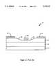
- FIG. 1shows a cross-sectional view of a general purpose MESFET IC 10 wherein three types of MESFET structures 20, 30 and 40 are supported on a semi-insulating GaAs substrate 50.
- Each of these structureshas a source, i.e., 22, 32, 42, a gate, i.e. 24, 34, and 44, and a drain, i.e., 26, 36, and 46. Under these sources and the drains, these three MESFET structures all have highly doped and deep N-plus regions, regions 27, 37 and 47.
- all three structuresalso have a shallower active channel region, i.e., regions 28, 38, and 48, which extends partially into these deeper N-plus regions, i.e., regions 27, 37, and 47.
- the dopant concentrations of the shallower active channelsas represented by regions 28, 38, and 48.
- the region 28is a depletion and enhancement channel
- the region 38is an enhancement channel
- the region 48is a depletion channel.
- FET structuresillustrate that when the active channel under the gate, i.e., regions 28,38, and 48, have lower concentration of dopant, i.e., the E-FET and D-FET types of structures, there is a higher breakdown voltage.
- the lower concentration of dopant in these type of structuresalso causes the source-drain current to decrease. There seems to have a conflict between these two design parameters with these conventional types of structures that the breakdown voltage and the source to drain current can not be increased simultaneously.
- Codella et al.disclose in U.S. Pat. No. 4,632,822 a self aligned GaAs, lightly doped drain MESFET wherein a shallow N-minus (N-) active channel region formed on a GaAs substrate, a Schottky gate overlaying the N- region and highly doped and deep N+ source and drain regions formed on either side of the gate.
- N-N-minus
- n-type source/drain extensionswhich have intermediate depth and doping concentration to minimize the device series resistance, suppress short channel effects and permit channel length reduction to sub micron levels.
- Codella et al.also disclose a structure where a deep p-type pockets are formed under the source/drain extensions to better control the device threshold voltage and to further reduce the channel.
- the GaAs MESFET self-aligned structure as disclosed by Codellais able to reduce the series resistance and shorten the channel length by the use lightly doped source/drain extensions which diminishes the short channel effects by preventing the drain electric field to extend into the active channel underneath the gate.
- the dopant concentration of the lightly doped region in the gate extension areasis too low to generate a high drain-source current as required by the power GaAs MESFET.
- FIG. 2represents such an structure where a cross sectional view of the proposed FET structure 70 is shown.
- the IC structureis built on a semi-insulating GaAs substrate 75 with an overlaying buffer 80.
- This is structure according to Hasegawawill increase the drain breakdown voltage.
- such structurehas only limited applications and is not suitable for use in low noise power amplifier which does not provide a solution to overcome the difficulty in implementing GaAs ICs in power MESFET circuits.
- Another object of the present inventionis to provide a FET structure and fabrication method to produce GaAs power MESFET with high breakdown voltage and drain to source current without the use of complicate processing steps.
- Another object of the present inventionis to provide a FET structure and fabrication method to produce GaAs power MESFET with high breakdown voltage and drain to source current where the processing steps are relatively simple and can be reliably repeated.
- the present inventioncomprises a metal semiconductor field effect transistor (MESFET).
- the MESFETcomprises a semiconductor substrate having a top surface.
- the MESFETfurther comprises a contiguous source area, gate area, and drain area disposed near the top surface on the semiconductor substrate, wherein the source and drain areas is of an equal relatively large depth from the top surface with high doping concentration.
- the gate areais of a relatively small depth from the top surface.
- the gate areais further disposed between and extending thereunto the source area and the drain area.
- the gate areafurther includes a current enhancement region with relatively lighter dopant concentration and extends between the gate and the source area.
- Another advantage of the present inventionis that it provides a FET structure and fabrication method to produce GaAs power MESFET with high breakdown voltage and drain to source current without the use of complicate processing steps.
- Another advantage of the present inventionis that it provides a FET structure and fabrication method to produce GaAs power MESFET with high breakdown voltage and drain to source current where the processing steps are relatively simple and can be reliably repeated.
- FIG. 1is a cross-sectional view of a prior art general purpose MESFET IC structure
- FIG. 2is a cross-sectional view of another prior art MESFET IC structure
- FIG. 3is a cross-sectional view of a GaAs power MESFET IC structure according to the present invention.
- FIG. 4A-4Eare diagrams illustrating by sequential cross-sectional representations the process steps of the present invention in making the MESFET IC structure as shown in FIG. 3.
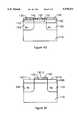
- FIG. 3shows a cross-sectional view of one preferred embodiment of a power GaAs MESFET device 100 in accordance with the principles and the fabrication processes of the present invention.
- a GaAs substrate 110is used to support this MESFET device 100 thereon.
- the MESFET devicecomprises a source electrode 115, a gate electrode 120 and a drain electrode 125.
- the ohmic contacts for the source electrode 115 and the drain 125 electrodeare 130 and 140 respectively which are composed of AuGeNi compound.
- the gate Schottky contact 135is composed of a TiPtAu compound.
- the source ohmic contact 130 and the drain ohmic contact 145are separated from the gate Schottky contact 135 by silicon nitride (Si 3 N 4 ) barrier 145 and 150 receptively.
- an enhancement implanted conducelye region (N-) 155Underneath the gate Schottky contact 135, the silicon nitride barrier 145, and the source ohmic contact 130 is an enhancement implanted conductlye region (N-) 155.
- the region 155extends slightly to the right beyond the gate Schottky contact 120 and cover a small region beneath the silicon nitride barrier 150.
- a layer of depletion implanted conductive region (N-) 160lies underneath the entire length of the MESFET device 100 which extends from a region which is directly underneath the left end of the enhancement implanted conductive region 155 to the right end directly underneath the drain ohmic contact 140.
- the active channel between the pockets 165 and 170is referred to as a gate area 164.
- the gate area 164comprises partially the depletion implanted region 160 and
- This inventionthus discloses a metal semiconductor field effect transistor (MESFET) 100 which comprises a semiconductor substrate 110 composed of gallium arsenide (GaAs) which has a top surface.
- This MESFET transistor 100further comprises a contiguous source area 165, gate area 164, and drain area 170 disposed near the top surface on the semiconductor substrate 110, wherein the source and drain areas 165 and 170 respectively are of an equal relatively large depth from the top surface with high doping concentration.
- the dopantcan be either N-type or P-type dopants depending on practical design considerations of the specific application.
- the gate area 164is of a relatively small depth from the top surface.
- the gate area 164is further disposed between and extending thereunto the source area 165 and the drain area 170.
- the gate area 164further includes a current enhancement region 155 being doped with relatively lower dopant concentration and extending between the gate area 164 and the source area 165.
- the dopantscan be either of N-type or P-type dopants most suitable for specific implementations.
- the current enhancement region 155is a region of less depth from the top surface doped with both depletion implantation and enhancement implantation.
- the gate area 164further includes a breakdown prevention region doped with a depletion implantation which a relatively less dopant concentration. The breakdown prevention region extends between the gate 135 and the drain area 170.
- This novel power MESFET device 100 shown in FIG. 3has several advantageous features.
- the conductive channel between the source electrode 115 and the gate electrode 120i.e., the gate area 164, is now a conductive region composed of twice implanted zones, i.e., the enhancement implemented region 155 and the depletion implanted region 160. Higher drain to source current can be generated now because the higher dopant concentration in this conductive channel.
- the channel between the gate electrode 120 and the drain electrode 125is a channel comprises only depletion implanted region 160.
- the MESFET device 100has a high drain breakdown voltage because of this configuration due to the fact that there is only a relatively lightly doped depletion implanted region 160 serves as active channel between the drain electrode 125 and the gate electrode 120.
- the structure of the MESFET device 100 near the gate electrode 120 and the drain electrode 125can resist a higher level of reverse voltage which causes the drain breakdown voltage to increase.
- the GaAs power MESFET device 100 as shown in FIG. 3is fabricated by the processing steps as described below with each step described sequentially with one of the pictures in FIGS. 4A to 4E.
- the fabrication processis initiated starting from a semi-insulating undoped or chromium doped GaAs substrate 110 upon which the active areas 165 and 170 of n-type conductivity is formed.
- This stepconsists of first forming a passivation surface layer 167 over the substrate 110 with a dielectric material such as silicon nitride (Si3N4). Photoresist patterns are then used to select the areas of substrate where the device active layer is to be formed wherein the n-plus type ions such as silicon is implanted directly into the resist free areas.
- a depletion implantation over the entire active area of the MESFET device 100is performed.
- the energy and dose of the ions implantedare chosen such that the semiconducting N-GaAs layer 160 as the result of this ion implantation operation is shallow having a depth of approximately 0.1 micron and has a dopant concentration in the range of about 10 16 to 10 17 atoms/cm 3 .
- the right portion of the top area above the depletion implanted region 160is covered with a photo-resist 162. Then a enhancement ion implantation is performed on the uncovered area to form an enhancement implanted region 155 on top of the depletion implanted region 160 over the left portion on the top surface of the MESFET device 100 where it is not covered by the photo-resist 162.
- the enhancement ion implantation layer 155has an dopant concentration in the range of 10 16 to 10 17 atoms/cm 3 with a layer thickness of approximately 0.1 microns.
- a method for fabricating a metal semiconductor field effect transistor (MESFET) 100 with higher breakdown voltage and greater drain to source currentis also disclosed in the present invention.
- the method for fabricating this power MESFET 100comprises the steps of (a) forming a passivation dielectric layer on top of a semiconductor substrate; (b) forming two-large depth active areas under the dielectric layer by utilizing a photoresist for defining and implanting ions of a first conductivity with higher doping concentration into the active areas wherein one of the active areas being a source area and another a drain area; (c) forming a shallow depth low-doping gate channel by implanting the entire active area using a lower doping concentration with ions of the first conductivity; (d) defining a current enhancement region by employing a photoresist to cover the top surface above the source area and a small portion of contiguous top surface above the gate channel; (e) performing a shallow-depth low concentration enhancement ion implantation for the current enhancement region with ions of the first conductivity
Landscapes
- Junction Field-Effect Transistors (AREA)
Abstract
Description
TABLE 1 ______________________________________ Breakdown Structure Implantation Voltage Ids ______________________________________ E-FET Enhancement Implantation High Low D-FET Depletion Implantation High Medium M-FET Enhancement and Depletion Low High ______________________________________
Claims (1)
Priority Applications (1)
| Application Number | Priority Date | Filing Date | Title |
|---|---|---|---|
| US08/401,017US5578512A (en) | 1993-09-07 | 1995-03-08 | Power MESFET structure and fabrication process with high breakdown voltage and enhanced source to drain current |
Applications Claiming Priority (2)
| Application Number | Priority Date | Filing Date | Title |
|---|---|---|---|
| US11691893A | 1993-09-07 | 1993-09-07 | |
| US08/401,017US5578512A (en) | 1993-09-07 | 1995-03-08 | Power MESFET structure and fabrication process with high breakdown voltage and enhanced source to drain current |
Related Parent Applications (1)
| Application Number | Title | Priority Date | Filing Date |
|---|---|---|---|
| US11691893ADivision | 1993-09-07 | 1993-09-07 |
Publications (1)
| Publication Number | Publication Date |
|---|---|
| US5578512Atrue US5578512A (en) | 1996-11-26 |
Family
ID=22370028
Family Applications (1)
| Application Number | Title | Priority Date | Filing Date |
|---|---|---|---|
| US08/401,017Expired - LifetimeUS5578512A (en) | 1993-09-07 | 1995-03-08 | Power MESFET structure and fabrication process with high breakdown voltage and enhanced source to drain current |
Country Status (1)
| Country | Link |
|---|---|
| US (1) | US5578512A (en) |
Cited By (14)
| Publication number | Priority date | Publication date | Assignee | Title |
|---|---|---|---|---|
| US6146931A (en)* | 1997-12-02 | 2000-11-14 | Fujitsu Quantum Devices Limited | Method of forming a semiconductor device having a barrier layer interposed between the ohmic contact and the schottky contact |
| US6150680A (en)* | 1998-03-05 | 2000-11-21 | Welch Allyn, Inc. | Field effect semiconductor device having dipole barrier |
| US6458640B1 (en) | 2001-06-04 | 2002-10-01 | Anadigics, Inc. | GaAs MESFET having LDD and non-uniform P-well doping profiles |
| US20030006455A1 (en)* | 2001-06-14 | 2003-01-09 | Ixys Corporation | Semiconductor devices having group III-V compound layers |
| US20050009277A1 (en)* | 2003-03-11 | 2005-01-13 | Mosel Vitelic, Inc. | Termination structure of DMOS device and method of forming the same |
| WO2006083577A1 (en)* | 2005-02-04 | 2006-08-10 | Raytheon Company | Monolithic integrated circuit having three field effect transistors |
| US20060175631A1 (en)* | 2005-02-04 | 2006-08-10 | Raytheon Company | Monolithic integrated circuit having enhanced breakdown voltage |
| US20060223293A1 (en)* | 2005-04-01 | 2006-10-05 | Raytheon Company | Semiconductor devices having improved field plates |
| US20070138515A1 (en)* | 2005-12-19 | 2007-06-21 | M/A-Com, Inc. | Dual field plate MESFET |
| US20070155072A1 (en)* | 2006-01-05 | 2007-07-05 | M/A-Com, Inc. | Method for fabricating a MESFET |
| CN105161531A (en)* | 2015-08-26 | 2015-12-16 | 西安电子科技大学 | 4h-sic metal semiconductor field effect transistor and manufacturing method thereof |
| CN105789056A (en)* | 2016-04-22 | 2016-07-20 | 西安电子科技大学 | Method of preparing 4H-SiC metal semiconductor field effect transistor with part highly-doped channel |
| CN113257887A (en)* | 2021-03-23 | 2021-08-13 | 西安电子科技大学 | 4H-SiC metal semiconductor field effect transistor with three regions |
| US11289600B2 (en) | 2019-05-17 | 2022-03-29 | Electronics And Telecommunications Research Institute | Field effect transistor |
Citations (7)
| Publication number | Priority date | Publication date | Assignee | Title |
|---|---|---|---|---|
| US4694563A (en)* | 1981-01-29 | 1987-09-22 | Sumitomo Electric Industries, Ltd. | Process for making Schottky-barrier gate FET |
| US4698899A (en)* | 1983-10-19 | 1987-10-13 | Gould Inc. | Field effect transistor |
| US4729372A (en)* | 1983-11-17 | 1988-03-08 | Lri L.P. | Apparatus for performing ophthalmic laser surgery |
| US4753899A (en)* | 1986-01-28 | 1988-06-28 | Telefunken Electronic Gmbh | Process for the fabrication of a Schottky gate field-effect transistor having a submicron effective channel length |
| US4941093A (en)* | 1985-09-12 | 1990-07-10 | Summit Technology, Inc. | Surface erosion using lasers |
| EP0417952A2 (en)* | 1989-09-05 | 1991-03-20 | Colloptics, Inc. | Shaping using area patterning mask |
| WO1992000711A1 (en)* | 1990-07-07 | 1992-01-23 | Aesculap Ag | Process and device for modelling or correcting optical lenses, especially the cornea of the eye |
- 1995
- 1995-03-08USUS08/401,017patent/US5578512A/ennot_activeExpired - Lifetime
Patent Citations (7)
| Publication number | Priority date | Publication date | Assignee | Title |
|---|---|---|---|---|
| US4694563A (en)* | 1981-01-29 | 1987-09-22 | Sumitomo Electric Industries, Ltd. | Process for making Schottky-barrier gate FET |
| US4698899A (en)* | 1983-10-19 | 1987-10-13 | Gould Inc. | Field effect transistor |
| US4729372A (en)* | 1983-11-17 | 1988-03-08 | Lri L.P. | Apparatus for performing ophthalmic laser surgery |
| US4941093A (en)* | 1985-09-12 | 1990-07-10 | Summit Technology, Inc. | Surface erosion using lasers |
| US4753899A (en)* | 1986-01-28 | 1988-06-28 | Telefunken Electronic Gmbh | Process for the fabrication of a Schottky gate field-effect transistor having a submicron effective channel length |
| EP0417952A2 (en)* | 1989-09-05 | 1991-03-20 | Colloptics, Inc. | Shaping using area patterning mask |
| WO1992000711A1 (en)* | 1990-07-07 | 1992-01-23 | Aesculap Ag | Process and device for modelling or correcting optical lenses, especially the cornea of the eye |
Cited By (22)
| Publication number | Priority date | Publication date | Assignee | Title |
|---|---|---|---|---|
| US6146931A (en)* | 1997-12-02 | 2000-11-14 | Fujitsu Quantum Devices Limited | Method of forming a semiconductor device having a barrier layer interposed between the ohmic contact and the schottky contact |
| US6150680A (en)* | 1998-03-05 | 2000-11-21 | Welch Allyn, Inc. | Field effect semiconductor device having dipole barrier |
| US6458640B1 (en) | 2001-06-04 | 2002-10-01 | Anadigics, Inc. | GaAs MESFET having LDD and non-uniform P-well doping profiles |
| US20030006455A1 (en)* | 2001-06-14 | 2003-01-09 | Ixys Corporation | Semiconductor devices having group III-V compound layers |
| US6734476B2 (en) | 2001-06-14 | 2004-05-11 | Ixys Corporation | Semiconductor devices having group III-V compound layers |
| US20050009277A1 (en)* | 2003-03-11 | 2005-01-13 | Mosel Vitelic, Inc. | Termination structure of DMOS device and method of forming the same |
| US6989306B2 (en) | 2003-03-11 | 2006-01-24 | Mosel Vitelic, Inc. | Termination structure of DMOS device and method of forming the same |
| JP2008530781A (en)* | 2005-02-04 | 2008-08-07 | レイセオン・カンパニー | Monolithic integrated circuit having three field effect transistors |
| WO2006083577A1 (en)* | 2005-02-04 | 2006-08-10 | Raytheon Company | Monolithic integrated circuit having three field effect transistors |
| US20060175631A1 (en)* | 2005-02-04 | 2006-08-10 | Raytheon Company | Monolithic integrated circuit having enhanced breakdown voltage |
| US20060175632A1 (en)* | 2005-02-04 | 2006-08-10 | Raytheon Company | Monolithic integrated circuit having enhancement mode/depletion mode field effect transistors and RF/RF/microwave/milli-meter wave milli-meter wave field effect transistors |
| US7626218B2 (en) | 2005-02-04 | 2009-12-01 | Raytheon Company | Monolithic integrated circuit having enhancement mode/depletion mode field effect transistors and RF/RF/microwave/milli-meter wave milli-meter wave field effect transistors |
| US20060223293A1 (en)* | 2005-04-01 | 2006-10-05 | Raytheon Company | Semiconductor devices having improved field plates |
| US20070166888A1 (en)* | 2005-04-01 | 2007-07-19 | Kiuchul Hwang | Semiconductor devices having improved field plates |
| US7498223B2 (en) | 2005-04-01 | 2009-03-03 | Raytheon Company | Semiconductor devices having improved field plates |
| US20070138515A1 (en)* | 2005-12-19 | 2007-06-21 | M/A-Com, Inc. | Dual field plate MESFET |
| US20070155072A1 (en)* | 2006-01-05 | 2007-07-05 | M/A-Com, Inc. | Method for fabricating a MESFET |
| US7485514B2 (en)* | 2006-01-05 | 2009-02-03 | Winslow Thomas A | Method for fabricating a MESFET |
| CN105161531A (en)* | 2015-08-26 | 2015-12-16 | 西安电子科技大学 | 4h-sic metal semiconductor field effect transistor and manufacturing method thereof |
| CN105789056A (en)* | 2016-04-22 | 2016-07-20 | 西安电子科技大学 | Method of preparing 4H-SiC metal semiconductor field effect transistor with part highly-doped channel |
| US11289600B2 (en) | 2019-05-17 | 2022-03-29 | Electronics And Telecommunications Research Institute | Field effect transistor |
| CN113257887A (en)* | 2021-03-23 | 2021-08-13 | 西安电子科技大学 | 4H-SiC metal semiconductor field effect transistor with three regions |
Similar Documents
| Publication | Publication Date | Title |
|---|---|---|
| US4636823A (en) | Vertical Schottky barrier gate field-effect transistor in GaAs/GaAlAs | |
| US4471366A (en) | Field effect transistor with high cut-off frequency and process for forming same | |
| JP3082671B2 (en) | Transistor element and method of manufacturing the same | |
| KR100854078B1 (en) | Morse gate type power semiconductor device and manufacturing method thereof | |
| US4115793A (en) | Field effect transistor with reduced series resistance | |
| US7378708B2 (en) | Transistor having a protruded drain | |
| US5578512A (en) | Power MESFET structure and fabrication process with high breakdown voltage and enhanced source to drain current | |
| US20020005559A1 (en) | Lateral semiconductor device | |
| KR910002037B1 (en) | Semiconductor device and manufacturing method | |
| KR960012539A (en) | Semiconductor device and manufacturing method | |
| KR930009101A (en) | Improved horizontally lateral double-diffusion MOS transistor and its manufacturing method | |
| US4952991A (en) | Vertical field-effect transistor having a high breakdown voltage and a small on-resistance | |
| JP3509896B2 (en) | Semiconductor device | |
| JPH03109775A (en) | Insulation-gate-type semiconductor device | |
| US5723349A (en) | Process for manufacturing a high conductivity insulated gate bipolar transistor integrater structure | |
| US5877047A (en) | Lateral gate, vertical drift region transistor | |
| EP0283878A1 (en) | Field effect transistor | |
| KR100521994B1 (en) | Trench gate type MOS transistor and its manufacturing method | |
| JPS6327062A (en) | Mis field-effect transistor | |
| JPS6085567A (en) | Field-effect transistor | |
| JP3167046B2 (en) | Static induction semiconductor device | |
| KR100264733B1 (en) | V-mos semiconductor device and method of manufacturing the same | |
| JPH07135219A (en) | Field effect transistor | |
| KR930010117B1 (en) | Semiconductor device of bimes structure | |
| KR100264732B1 (en) | V-MOS semiconductor device and manufacturing method thereof |
Legal Events
| Date | Code | Title | Description |
|---|---|---|---|
| AS | Assignment | Owner name:INDUSTRIAL TECHNOLOGY RESEARCH INSTITUTE, TAIWAN Free format text:ASSIGNMENT OF ASSIGNORS INTEREST;ASSIGNOR:TAO, KUANG-CHUNG;REEL/FRAME:007393/0664 Effective date:19950303 | |
| STCF | Information on status: patent grant | Free format text:PATENTED CASE | |
| REMI | Maintenance fee reminder mailed | ||
| FPAY | Fee payment | Year of fee payment:4 | |
| SULP | Surcharge for late payment | ||
| FEPP | Fee payment procedure | Free format text:PAYOR NUMBER ASSIGNED (ORIGINAL EVENT CODE: ASPN); ENTITY STATUS OF PATENT OWNER: LARGE ENTITY | |
| AS | Assignment | Owner name:VIA TECHNOLOGIES, INC., TAIWAN Free format text:ASSIGNMENT OF ASSIGNORS INTEREST;ASSIGNOR:INDUSTRIAL TECHNOLOGY RESEARCH INSTITUTE;REEL/FRAME:014815/0903 Effective date:20031203 | |
| FPAY | Fee payment | Year of fee payment:8 | |
| FPAY | Fee payment | Year of fee payment:12 | |
| REMI | Maintenance fee reminder mailed | ||
| FEPP | Fee payment procedure | Free format text:PAYER NUMBER DE-ASSIGNED (ORIGINAL EVENT CODE: RMPN); ENTITY STATUS OF PATENT OWNER: LARGE ENTITY Free format text:PAYOR NUMBER ASSIGNED (ORIGINAL EVENT CODE: ASPN); ENTITY STATUS OF PATENT OWNER: LARGE ENTITY | |
| AS | Assignment | Owner name:BLU TECHNOLOGY 2 LLC, MALAYSIA Free format text:ASSIGNMENT OF ASSIGNORS INTEREST;ASSIGNOR:VIA TECHNOLOGIES, INC.;REEL/FRAME:021912/0830 Effective date:20080924 | |
| AS | Assignment | Owner name:VIA TECHNOLOGIES, INC., TAIWAN Free format text:CONFIRMATORY ASSIGNMENT OF PATENT RIGHTS;ASSIGNOR:INDUSTRIAL TECHNOLOGY RESEARCH INSTITUTE;REEL/FRAME:021962/0989 Effective date:20081009 |