US5576629A - Plasma monitoring and control method and system - Google Patents
Plasma monitoring and control method and systemDownload PDFInfo
- Publication number
- US5576629A US5576629AUS08/328,069US32806994AUS5576629AUS 5576629 AUS5576629 AUS 5576629AUS 32806994 AUS32806994 AUS 32806994AUS 5576629 AUS5576629 AUS 5576629A
- Authority
- US
- United States
- Prior art keywords
- plasma
- electronic device
- radio frequency
- fabrication
- frequency power
- Prior art date
- Legal status (The legal status is an assumption and is not a legal conclusion. Google has not performed a legal analysis and makes no representation as to the accuracy of the status listed.)
- Expired - Lifetime
Links
- 238000000034methodMethods0.000titleclaimsabstractdescription345
- 238000012544monitoring processMethods0.000titleclaimsabstractdescription26
- 230000008569processEffects0.000claimsabstractdescription278
- 238000005441electronic device fabricationMethods0.000claimsabstractdescription61
- 238000004886process controlMethods0.000claimsabstractdescription48
- 238000001514detection methodMethods0.000claimsabstractdescription34
- 238000004519manufacturing processMethods0.000claimsdescription86
- 238000005259measurementMethods0.000claimsdescription43
- 238000012545processingMethods0.000claimsdescription26
- 230000007246mechanismEffects0.000claimsdescription21
- 230000004044responseEffects0.000claimsdescription17
- 238000010606normalizationMethods0.000claimsdescription15
- 238000012360testing methodMethods0.000claimsdescription14
- 238000012417linear regressionMethods0.000claimsdescription8
- 238000012935AveragingMethods0.000claimsdescription7
- 230000000670limiting effectEffects0.000claimsdescription4
- 230000000977initiatory effectEffects0.000claims6
- 238000011022operating instructionMethods0.000claims1
- 230000008021depositionEffects0.000abstractdescription13
- 230000006870functionEffects0.000abstractdescription9
- 235000012431wafersNutrition0.000description32
- 238000004422calculation algorithmMethods0.000description28
- 230000008901benefitEffects0.000description14
- 239000007789gasSubstances0.000description14
- 238000000151depositionMethods0.000description12
- 238000003070Statistical process controlMethods0.000description11
- 230000008859changeEffects0.000description11
- 239000004065semiconductorSubstances0.000description8
- 229910021420polycrystalline siliconInorganic materials0.000description7
- 229920005591polysiliconPolymers0.000description7
- 238000004458analytical methodMethods0.000description6
- 238000005516engineering processMethods0.000description6
- 238000010586diagramMethods0.000description5
- 238000011065in-situ storageMethods0.000description5
- 230000001939inductive effectEffects0.000description5
- 238000000623plasma-assisted chemical vapour depositionMethods0.000description5
- 230000003595spectral effectEffects0.000description5
- 239000000463materialSubstances0.000description4
- 238000010168coupling processMethods0.000description3
- 238000009434installationMethods0.000description3
- 238000005457optimizationMethods0.000description3
- 230000009467reductionEffects0.000description3
- 238000001228spectrumMethods0.000description3
- 238000010183spectrum analysisMethods0.000description3
- BOTDANWDWHJENH-UHFFFAOYSA-NTetraethyl orthosilicateChemical compoundCCO[Si](OCC)(OCC)OCCBOTDANWDWHJENH-UHFFFAOYSA-N0.000description2
- 230000002411adverseEffects0.000description2
- 238000004364calculation methodMethods0.000description2
- 238000004140cleaningMethods0.000description2
- 230000008878couplingEffects0.000description2
- 238000005859coupling reactionMethods0.000description2
- 230000007423decreaseEffects0.000description2
- 230000003247decreasing effectEffects0.000description2
- 238000013461designMethods0.000description2
- 238000002474experimental methodMethods0.000description2
- 238000001914filtrationMethods0.000description2
- 230000006872improvementEffects0.000description2
- 230000001965increasing effectEffects0.000description2
- 238000012423maintenanceMethods0.000description2
- 239000000203mixtureSubstances0.000description2
- 229920002120photoresistant polymerPolymers0.000description2
- 239000000523sampleSubstances0.000description2
- 230000035945sensitivityEffects0.000description2
- 238000013179statistical modelMethods0.000description2
- 239000000758substrateSubstances0.000description2
- 238000012546transferMethods0.000description2
- XUIMIQQOPSSXEZ-UHFFFAOYSA-NSiliconChemical compound[Si]XUIMIQQOPSSXEZ-UHFFFAOYSA-N0.000description1
- 238000000540analysis of varianceMethods0.000description1
- 238000002048anodisation reactionMethods0.000description1
- 238000013459approachMethods0.000description1
- 238000010923batch productionMethods0.000description1
- 230000015572biosynthetic processEffects0.000description1
- 238000000576coating methodMethods0.000description1
- 238000005137deposition processMethods0.000description1
- 238000012625in-situ measurementMethods0.000description1
- 238000010849ion bombardmentMethods0.000description1
- 238000012986modificationMethods0.000description1
- 230000004048modificationEffects0.000description1
- 238000006116polymerization reactionMethods0.000description1
- 230000002028prematureEffects0.000description1
- 238000012797qualificationMethods0.000description1
- 230000002829reductive effectEffects0.000description1
- 238000012827research and developmentMethods0.000description1
- 238000005096rolling processMethods0.000description1
- 229910052710siliconInorganic materials0.000description1
- 239000010703siliconSubstances0.000description1
- 239000007787solidSubstances0.000description1
- 238000004544sputter depositionMethods0.000description1
- 238000010561standard procedureMethods0.000description1
- 238000007619statistical methodMethods0.000description1
- 230000036962time dependentEffects0.000description1
- 230000007704transitionEffects0.000description1
- 230000001960triggered effectEffects0.000description1
Images


Classifications
- H—ELECTRICITY
- H01—ELECTRIC ELEMENTS
- H01J—ELECTRIC DISCHARGE TUBES OR DISCHARGE LAMPS
- H01J37/00—Discharge tubes with provision for introducing objects or material to be exposed to the discharge, e.g. for the purpose of examination or processing thereof
- H01J37/32—Gas-filled discharge tubes
- H01J37/32917—Plasma diagnostics
- H01J37/32935—Monitoring and controlling tubes by information coming from the object and/or discharge
- H01J37/32963—End-point detection
- B—PERFORMING OPERATIONS; TRANSPORTING
- B24—GRINDING; POLISHING
- B24B—MACHINES, DEVICES, OR PROCESSES FOR GRINDING OR POLISHING; DRESSING OR CONDITIONING OF ABRADING SURFACES; FEEDING OF GRINDING, POLISHING, OR LAPPING AGENTS
- B24B37/00—Lapping machines or devices; Accessories
- B24B37/005—Control means for lapping machines or devices
- B24B37/013—Devices or means for detecting lapping completion
- C—CHEMISTRY; METALLURGY
- C23—COATING METALLIC MATERIAL; COATING MATERIAL WITH METALLIC MATERIAL; CHEMICAL SURFACE TREATMENT; DIFFUSION TREATMENT OF METALLIC MATERIAL; COATING BY VACUUM EVAPORATION, BY SPUTTERING, BY ION IMPLANTATION OR BY CHEMICAL VAPOUR DEPOSITION, IN GENERAL; INHIBITING CORROSION OF METALLIC MATERIAL OR INCRUSTATION IN GENERAL
- C23C—COATING METALLIC MATERIAL; COATING MATERIAL WITH METALLIC MATERIAL; SURFACE TREATMENT OF METALLIC MATERIAL BY DIFFUSION INTO THE SURFACE, BY CHEMICAL CONVERSION OR SUBSTITUTION; COATING BY VACUUM EVAPORATION, BY SPUTTERING, BY ION IMPLANTATION OR BY CHEMICAL VAPOUR DEPOSITION, IN GENERAL
- C23C16/00—Chemical coating by decomposition of gaseous compounds, without leaving reaction products of surface material in the coating, i.e. chemical vapour deposition [CVD] processes
- C23C16/44—Chemical coating by decomposition of gaseous compounds, without leaving reaction products of surface material in the coating, i.e. chemical vapour deposition [CVD] processes characterised by the method of coating
- C23C16/52—Controlling or regulating the coating process
- H—ELECTRICITY
- H01—ELECTRIC ELEMENTS
- H01J—ELECTRIC DISCHARGE TUBES OR DISCHARGE LAMPS
- H01J37/00—Discharge tubes with provision for introducing objects or material to be exposed to the discharge, e.g. for the purpose of examination or processing thereof
- H01J37/32—Gas-filled discharge tubes
- H01J37/32009—Arrangements for generation of plasma specially adapted for examination or treatment of objects, e.g. plasma sources
- H01J37/32082—Radio frequency generated discharge
- H01J37/32091—Radio frequency generated discharge the radio frequency energy being capacitively coupled to the plasma
- H—ELECTRICITY
- H01—ELECTRIC ELEMENTS
- H01J—ELECTRIC DISCHARGE TUBES OR DISCHARGE LAMPS
- H01J37/00—Discharge tubes with provision for introducing objects or material to be exposed to the discharge, e.g. for the purpose of examination or processing thereof
- H01J37/32—Gas-filled discharge tubes
- H01J37/32009—Arrangements for generation of plasma specially adapted for examination or treatment of objects, e.g. plasma sources
- H01J37/32082—Radio frequency generated discharge
- H01J37/32174—Circuits specially adapted for controlling the RF discharge
- H01J37/32183—Matching circuits
- H—ELECTRICITY
- H01—ELECTRIC ELEMENTS
- H01J—ELECTRIC DISCHARGE TUBES OR DISCHARGE LAMPS
- H01J37/00—Discharge tubes with provision for introducing objects or material to be exposed to the discharge, e.g. for the purpose of examination or processing thereof
- H01J37/32—Gas-filled discharge tubes
- H01J37/32917—Plasma diagnostics
- H01J37/32935—Monitoring and controlling tubes by information coming from the object and/or discharge
- H—ELECTRICITY
- H01—ELECTRIC ELEMENTS
- H01J—ELECTRIC DISCHARGE TUBES OR DISCHARGE LAMPS
- H01J37/00—Discharge tubes with provision for introducing objects or material to be exposed to the discharge, e.g. for the purpose of examination or processing thereof
- H01J37/32—Gas-filled discharge tubes
- H01J37/32917—Plasma diagnostics
- H01J37/3299—Feedback systems
- H—ELECTRICITY
- H01—ELECTRIC ELEMENTS
- H01L—SEMICONDUCTOR DEVICES NOT COVERED BY CLASS H10
- H01L22/00—Testing or measuring during manufacture or treatment; Reliability measurements, i.e. testing of parts without further processing to modify the parts as such; Structural arrangements therefor
- H01L22/20—Sequence of activities consisting of a plurality of measurements, corrections, marking or sorting steps
- H01L22/26—Acting in response to an ongoing measurement without interruption of processing, e.g. endpoint detection, in-situ thickness measurement
- H—ELECTRICITY
- H01—ELECTRIC ELEMENTS
- H01J—ELECTRIC DISCHARGE TUBES OR DISCHARGE LAMPS
- H01J2237/00—Discharge tubes exposing object to beam, e.g. for analysis treatment, etching, imaging
- H01J2237/32—Processing objects by plasma generation
- H01J2237/33—Processing objects by plasma generation characterised by the type of processing
- H01J2237/334—Etching
Definitions
- the present inventionrelates to methods of monitoring and controlling the fabrication of an electronic device and, particularly, to a method and system for plasma monitoring and control that provides monitoring and control of radio frequency power including monitoring and control of radio frequency voltage, current, and phase angle, as well as harmonics of theses parameters as they affect the production of radio frequency plasma.
- FIG. 1shows RF network 10 that produces RF power for an electronic device and fabrication reactor.
- RF power generator 12connects to local automated matching network 14 via cable 16. From local automated matching network 14, mechanical RF connection 18 goes to process chamber 20.
- Process chamber 20includes cathode 22 that affects process gas 24 within plasma sheath 26 to produce an RF plasma.
- RF network 10In RF network 10, certain limitations exist. For example, RF power generator 12, while including solid state technology, still is a bulky system that consumes an undesirable about of clean room floor space. As a result, performance of RF network 10 is often adversely affected by installation dependencies due to generator placement.
- the objective of local automated matching network 14is to provide an efficient transfer of RF power from the RF power generator 12 to the RF load of plasma process gas 24 by matching the widely different impedances between RF power generator 12 and process chamber 20 (the RF load). Unfortunately, this match is accomplished by non-ideal impedance elements. This is particularly unfortunate considering the fact that impedance monitoring is a fundamental criterion in a frequency bands of interest to semiconductor plasma processing.
- a further limitation of RF network 10relates to process chamber 20 itself.
- the electronic devicesuch as a semiconductor wafer, is positioned and processed to achieve some desired result such as etch or deposition.
- process chamber 20two significant limitations exist. First of all, even with known installation dependencies and variability due to the local automated matching network 14, the RF power is primarily controlled based on a measurement made at RF power generator 12. Furthermore, even though RF power generator 12 for a given power level consists of three variables of voltage, current and phase angle, known systems generally measure and control RF power with the unit of watts only.
- FIGS. 2 and 3illustrate the limitations that exist when RF load power is measured only in terms of watts.
- diagram 30that includes origin 32 having axes 34, 36 and 38.
- Axis 38denotes the power level for RF power from RF power generator 12.
- three-dimensional object 40depicts the variability that exists with a one-dimensional measure of power.
- axis 34for example, represents changes in voltage for a given power level
- axis 36represents variation in current at the same power level.
- FIG. 2illustrates, for a given power level and minimum reflected load power considerable variability in current and voltage is possible.
- FIG. 2does not even consider phase angle differences.
- FIG. 3shows an actual measurement example of changes that can occur with a given power level in the three variables of voltage, current and phase angle.
- three-dimensional plot 50shows on axis 52 changes in phase angle between -81 and -87 degrees.
- On axis 54appears a scale of RMS current, A RMS ranging from 1.40 to 1.56 A RMS .
- Along axis 56are voltage measurements between 522 and 528 V RMS .
- measurement point 58indicates, for a given minimum RF power to process chamber 20, measurement points 58 exhibit a significant amount of variability. This obviously can significantly affect RF plasma measurement within process chamber 20.
- Local automated matching network 14 of RF network 10may be one of a wide variety of designs, all of which operate by tuning to a minimum reflected power.
- the dead band concept of matching circuit tuning, where inductive and/or capacitive elements are varied which drive the circuit to an acceptable reflected power levelis essentially the concept that FIG. 2 depicts.
- FIGS. 2 and 3illustrate, this concept of only monitoring reflected power could produce an infinite number of voltage, current, and phase angle combinations. For these infinite combinations associated differences in plasma and process parameters relate.
- FIG. 3 illustratesis for a single requested forward/reflected power combination.
- data points 58show the potentially infinite combinations that a widely accepted plasma tool generates operating under nominal conditions.
- one aspect of the inventionis a method for monitoring the radio frequency power of the plasma in an electronic device fabrication reactor that includes the necessary components for and steps of first sensing the voltage of the radio frequency power that is directed into a plasma producing gas at the input to the plasma producing environment of the electronic device fabrication reactor.
- the methodsenses the current and the phase angle of the radio frequency power directed to the plasma producing gas at the input to the plasma producing environment.
- the methodmeasures the full load that the radio frequency power sees by measuring the full load impedance of the plasma producing environment.
- the full loadin one embodiment represents not only the discharge and sheath impedances, but also the chuck and wafer impedance, a primary ground path impedance, and a secondary ground path impedance associated with the fabrication reactor plasma environment.
- Another aspect of the present inventionis a method and system for controlling the fabrication of an electronic device by generating a process halt or go-no-go signal according to predetermined parameters of the plasma process environment in the fabrication reactor.
- the systemincludes the necessary components for inputting a plurality of process parameters regarding the electronic device process into a process control computer that has a plurality of process control instructions for controlling the processing of the electronic device.
- the systemimplements a process recipe step counter that associates with the plurality of process control instructions for the electronic device fabrication process.
- the process control computerreceives information regarding the electronic device fabrication environment.
- the method and systemfurther determine the completion of a predetermined monitor time for monitoring the processing of the electronic device. Then, a predetermined set of process parameters relating to the electronic device are averaged upon the determination of the completion of the predetermined monitor time.
- the method and systemdetermine the presence of a reference subtraction signal to indicate the presence of a reference subtraction instruction in the process control instructions.
- the reference informationis then subtracted from the average process parameters upon the determination of the presence of the reference subtraction signal according to the reference subtraction instruction.
- the systemchecks a plurality of control limits.
- the control limitsform a part of the plurality of process parameters for limiting the control of the electronic device fabrication process according to the subtracted reference information.
- the method and systemthen generate an out of control signal upon determining that one or more of the values of the subtracted reference information are beyond an associated one of a plurality of control limits.
- the method and systemthen generate a process halt, or go-no-go signal for the electronic device fabrication process control computer in response to the out of control signal.
- Still another aspect of the present inventionis a method and system for controlling the fabrication of an electronic device by generating an endpoint detection signal according to predetermined parameters of an electronic device fabrication reactor.
- the method and systeminclude the necessary steps and components for inputting a plurality of process parameters regarding the electronic device fabrication process into a process control computer.
- the process control computerincludes a plurality of process control instructions for controlling the processing of the electronic device fabrication.
- the method and systemthen implement a process recipe step counter associated with the plurality of process control instructions.
- By acquiring and storing within the process control computerinformation regarding the electronic device fabrication environment is obtained.
- the step of determining a plurality of normalized endpoint valuesoccurs using a plurality of endpoint normalization instructions.
- the systemtests for completion of a normalization time and, if such time has been completed, the system acquires a plurality of normalized process values associated with the electronic device fabrication process. Then, the method and system apply a plurality of endpoint detection tests to determine the existence of an endpoint in the electronic device fabrication process. Then, the steps of generating an output end signal upon detecting the process endpoint, starting an overetch clock upon the generation of the output endpoint signal occur. An overetch end signal is then generated at a predetermined point in time after starting the overetch clock. Once the process control computer realizes that an overetch end signal has been generated, the ongoing process steps for the electronic device fabrication process terminate.
- the present inventionhas application for a wide variety of electronic devices, for example, for semiconductor wafers, semiconductor memory devices, and CD-ROM and similar types of devices that may be formed within an electronic device fabrication reactor.
- meaningful statistics concerning the plasma process environmentmay be generated.
- This improved controlmakes a significantly greater amount of process economy and flexibility possible.
- the precision of plasma processing that the present invention providesmakes statistical process control (SPC) feasible for a wide variety of electronic device fabrication processes.
- SPCstatistical process control
- another aspect of the present inventionis the use of linear regression techniques, such as stepwise linear regression modeling, that generates statistics relative to the plasma processing environment. These statistics make possible modeling of the plasma process environment within the fabrication reactor process chamber meaningful for generating process control models. These models may be used to significantly increase process uniformity for electronic devices.
- radio frequency harmonic measurementsfor measuring the voltage, current, and phase angle of the radio frequency power into the plasma process load for electronic device process environment.
- harmonic valuesfor voltage, current, and phase angle of the radio frequency power
- the present inventionfurther uses, in one aspect, a closed loop automatic gain control feature for controlling voltage, current, and/or phase so that voltage, current, and/or phase angle signals are measurable and used for precise process control.
- the present inventionprovides numerous technical advantages that overcome limitations existing in known methods and systems for monitoring and controlling the plasma environment within a fabrication reactor.
- One technical advantage of the present inventionis the ability to monitor radio frequency power at the load of the radio frequency power generator. By determining the radio frequency power that the plasma environment actually sees, as opposed to the radio frequency power at the output of the radio frequency generator, a much more precise measurement of the radio frequency power into the plasma environment is obtained. This may make it practical to place the radio frequency generator remote from the fabrication reactor and even outside the clean room.
- Another technical advantage of the present inventionis that it improves the impedance matching of the electronic circuit that includes the plasma process.
- the present inventionprovides a much more accurate measure of the resistive and reactive loads that the radio frequency power generator sees. This permits much more precise matching of the impedance. This also improves the overall operation of the present system.
- Another technical advantage of the present inventionis that in measuring the radio frequency power to the plasma process chamber the present invention treats radio frequency power as a three-dimensional quantity consisting of voltage, current, and phase angle as opposed to the one-dimensional quantity that conventional systems measure. As such, the present invention improves the ability to control the radio frequency power to the plasma environment in a way that improves the repeatability of plasma processes.
- Still another technical advantage of the present inventionis that by providing functions such as go-no-go control, endpoint detection automated control, and statistical process control based on statistical models, the present invention generally improves the fabrication yields for any given plasma process.
- Still a further technical advantage of the present inventionis that by analyzing the harmonic amplitudes of voltage, current, and phase angle of the radio frequency power into the plasma process environment, the present invention provides a truly unique opportunity to establish real-time process optimization mechanism.
- the present inventionprovides the user with the ability to teach the plasma process or metrology system of the fabrication reactor an acceptable level of process performance to improve manufacturing process control for the electronic device.
- FIG. 1illustrates the radio frequency network for establishing a plasma process environment within an electronic device fabrication reactor
- FIGS. 2 and 3illustrate, respectively, theoretical and actual variations in radio frequency power component measurements for a given radio frequency power to the plasma process environment
- FIG. 4illustrates a spectral analysis technique that the present invention offers
- FIG. 5illustrates the radio frequency network of the present embodiment
- FIG. 6shows the full load measurement characteristics of the present embodiment
- FIG. 7illustrates the go-no-go decision support that harmonic signature analysis of the present embodiment provides and makes possible
- FIG. 8illustrates the variation in current between individual semiconductor wafers to illustrate the variability in statistical process control that the present embodiment makes possible
- FIG. 9depicts the go-no-go detection process flow of the present embodiment
- FIG. 10illustrates the endpoint detection process flow of the present embodiment
- FIG. 11depicts the endpoint capabilities that the present embodiment makes possible as a result of the increased sensitivity and speed of process parameter detection
- FIG. 12illustrates a Circuit "A" component of the present embodiment for the automated gain control function
- FIG. 13illustrates the Circuit "B” band pass filter circuitry of the present embodiment
- FIG. 14illustrates the detector circuit and output amplifier and logic operation circuitry that is repeated through the present embodiment as Circuit "C";
- FIG. 15shows the voltage sensor signal-current sensor signal input circuitry for generating the isolated output amp and arithmetic logic output of the present embodiment
- FIG. 16depicts the B1-4 circuitry for measuring the amplitude of voltage or current signals from the input circuitry of FIG. 15.
- FIG. 17shows the phase harmonic circuits of the present embodiment for measuring the phase angles of harmonics of the current and voltage signals from FIG. 16;
- FIGS. 18A and 18Bshow an inductive coupler and a voltage sensor, respectively, of the present embodiment
- FIGS. 19A, 19B and 19Cillustrate various stages in a plasma etch process that the present embodiment may monitor and control
- FIG. 20illustrates process control sensing that the present embodiment makes possible with respect to the various stages at plasma etch process of FIGS. 19A, 19B and 19C;
- FIGS. 21 through 33show results associated with an exemplary application of the present embodiment.
- aspects of the present embodimentinclude a spectral analysis technique that is practical for implementation in an electronic device fabrication environment and the control steps that use the improved process parameter measurement, such as endpoint detection, real-time statistical process control (SPC), and immediate go-no-go or halt signal processing.
- the present embodimentincorporates the concept of measuring the full load impedance for the process environment to more precisely sense changes in the plasma process environment.
- spectral analysis flow diagram 60shows distorted harmonic-rich high frequency signal 62 that the present embodiment passes through a spectral filter network 64 including f0 filter 66 and other frequency filters shown elliptically through to f4 filter 68, for example. From filter network 64, signal 62 goes to splitter network 70 which feeds mixer 72.
- the signal flow of FIG. 4illustrates a practical technique for making radio frequency power measurements for the radio frequency power flowing to the plasma process environment.
- the signal that comes from the radio frequency plasmais analogous to that from an FM radio signal.
- Radio frequency power generator 12for many plasma processes, generates a 13.56 MHz signal that has few or no harmonic signals. Since the radio frequency signal that reaches the sensors of the present embodiment are measured at the load, there is at that point a non-linear portion that has already shifted some of the radio frequency energy from the signal. This produces the distorted harmonic-rich frequency signal 62 of FIG. 4. This basic sine-wave shape, therefore, generates distorted results.
- the f0 filter circuit 66 on through f4 filter circuit 68are band pass filters that are selective to the harmonic frequencies of the fundamental frequency of interest (e.g., 13.56 MHz).
- Splitter 70permits selection of the filter circuit output. Consequently, in the circuit of FIG.
- splitter 70 outputgoes to multiplexer 72 at the selected harmonic frequency, e.g., 13.56 MHz, 27.12 MHz, 40.68 MHz, 54.24 MHz, or 67.80 MHz. Because of the filter circuit selectivity, the signal that goes to multiplexer 72 is a clean sine-wave signal. A simple magnitude detector, such a peak detector or RMS detector circuit may then be used to determine the magnitude of the signal.
- the method of FIG. 4overcomes methods based on digital signal processing (DSP) techniques.
- DSP-based methodstake the radio frequency power signals to a Fast Fourier transform (FFT) algorithm contained in a DSP unit.
- FFTFast Fourier transform
- this methodcould be the technique of choice.
- variability due to the nonlinear components of the techniquemay cause significant errors and even failure of the technique due to unacceptable measurement performance.
- the process of FIG. 4also is superior to nondirectional coupler technology for radio frequency signal measurements.
- Many matching circuitscurrently employ directional coupling technology to make one-dimensional forward and reflective power measurements.
- the object of directional coupler technologyis to sample the radio frequency wave form as it travels through a coupler device. The sampled wave form is then directed to some detector technology.
- the detector technologycan vary from a simple square law device to a much more complex spectrum analyzer.
- the inherent broad band nature of directional couplers and the fact that any detector will be subject to the first spectrum of incidental radio frequency signalspose limitations on this technique.
- the broad band naturelimits the type of information derivable by the directional coupler technique, because traditional detectors have no ability to frequency discriminate. This causes a loss of all information that is contained in the load's harmonic signature. As such, the directional coupler technique may reduce to only a one-dimensional measurement capability for the radio frequency power.
- Process 60 of FIG. 4incorporates the desirable attributes of both the FFT method and the directional coupling method to provide a process that inherently discriminates both forward and reflected power, as well as frequency components.
- the FFTin hardware so as not to degrade the signal by front end DSP-based signal processing, while at the same time deriving a "net" radio frequency current delivered to the load without convoluting the frequency information, it is possible to significantly improve the radio frequency power measurement in the plasma environment.
- Process 60 in FIG. 4provides the capability to frequency discriminate the components of radio frequency power, including voltage, current, and phase, so that a complete picture of the radio frequency load may be established and used with whatever precision is necessary for manufacturing process control.
- process 60results in distortion-free harmonic measurements. These harmonic measurements permit a detailed understanding of the relationship between the object being measured (i.e., the broad band radio frequency voltage, current and phase) and the entity being controlled from the measurements (i.e., the plasma process).
- the present embodimentemploys radio frequency harmonic analysis for the purpose of determining endpoint detection, statistical process control, and the existence of a go-no-go situation that may indicate an out-of-control process.
- the advantage of using harmonicsis that there is no dead band process control or tapering off in the measurements that result. This provides the most rapid or instantaneous process control for any plasma processing environment.
- the present embodimentanalyzes harmonic amplitudes and matches them to known good historical values using the simple mathematical algorithm.
- the parameters that the present embodiment employspermits modeling of plasma process parameters that can relate to stress, thickness, deposition rate and other parameters.
- FIG. 5shows the implementation of the present embodiment in radio frequency network 80 for significantly improving plasma process control.
- radio frequency power generator 12supplies local automated matching network 14 of radio frequency power through cable 16.
- Local automated matching network 14provides radio frequency power through mechanical radio frequency connection 18 to process chamber 20.
- process chamber 20Within process chamber 20 are cathode 22, plasma environment 24, and plasma sheath 26.
- Sensors 82provide, through connection 84, radio frequency's voltage, radio frequency, current, and phase angle information to process control computer 86.
- Process control computer 86includes the necessary instructions for achieving endpoint detection, real-time SPC, and immediate go-no-go functions for the plasma gas 24 environment of process chamber 20.
- Sensors 82 at the input to process chamber 20include a voltage probe that the present embodiment places at the point of application of the radio frequency power and references it to ground. As a consequence, if any of the voltage dropped across the load changes these changes appear as a change in the voltage of the radio frequency power into the cathode 22 that produces the plasma. Similarly, an inductive pick-up (see FIG. 18) wrapped around a primary radio frequency current carrier senses the current of the radio frequency power going into process chamber 20. Thus, if anything changes in the radio frequency load, such as the clearing off of a film of a wafer or a changing of a gas mixture, the voltage and current will change.
- the changesmay be very subtle, such as unintentional changes in a gas mixture or an unintentional clearing off of a film on the electronic device. It could be, for example, polymerization of the chamber wall or the wearing away of anodization coatings on various process chamber components. Since the radio frequency load is closely coupled to the current and voltage as well as the phase angle, due to capacitive and inductive effects, these changes will affect the plasma environment in the process chamber.
- FIG. 6shows process chamber 20 in a way to illustrate the radio frequency loads that the present embodiment considers in determining the full radio frequency load to the radio frequency power from radio frequency power generator 12.
- process chamber 20has connections that include vacuum pump connection 90 that removes from process chamber 20 process gases and spent plasma gasses.
- Gas input 92connects to plasma sheath 94 and provides process gases into process chamber 20.
- Sheath 94connects to ground 95 to form a primary ground path impedance.
- ground connection 95connects to process chamber 20 to form a secondary ground path impedance.
- Chuck 97 and wafer 98form a further radio frequency load impedance with process chamber 20.
- Connecting to chuck 98may be a helium-cooled inlet 99 and a connection to sensor suite 82 of the present embodiment.
- plasma discharge environment 103forms yet another radio frequency load impedance to the radio frequency power
- the impedances for the radio frequency plasma generation processinclude the chuck and wafer impedance, Z1, the discharge and sheath impedance within process chamber 20, Z2, the primary ground path impedance, Z3, and the secondary ground impedance, Z4.
- the present embodimenttherefore, realizes the existence of a full radio frequency load that includes various chamber components such as the wall chemistry, the plasma discharge, and the wafer itself.
- the present embodimentmakes possible resolving each of the impedances at the power electrode by isolating the radio frequency power voltage, current and phase angle measurement associated with a particular impedance. This makes it possible to identify which factors contribute to shifts in the overall radio frequency load of the radio frequency network.
- the harmonic signature-based go-no-go decision support capability importanceis shown in FIG. 7.
- the current harmonicsare labelled I0 through I4.
- the largest shift in I4provides an immediate indication of a process shift. This deviation is created by a shift in the complex impedance of the radio frequency load.
- FIG. 8detects the wafer-to-wafer SPC capability that the present embodiment makes possible.
- endpointi.e., end of process
- SPC "X-bar" chartsi.e., end of process traces
- the complex radio frequency measurement that the present embodiment makes possiblemay be made both transparent and acceptable to the end user.
- the analysis of harmonic amplitudesprovides a truly unique opportunity to establish a real-time process optimization tool.
- the present embodimentmakes possible a go-no-go decision support capability. The essence of the go-no-go or halt process decision support capability to autonomously, and in real-time, evaluate process optimization and halt the operation on the semiconductor or electronic device should a predetermined out-of-control condition be detected.
- FIG. 9shows in more detail the go-no-go detection process flow 100 that the present embodiment employs.
- a userinputs operating parameters.
- process recipe step counterbegins.
- Data acquisitionbegins at block 106 and data is stored in a hard disk drive 108 associated with, for example, process control computer 86.
- the next stepis to test whether the monitored time has been completed as query 110 indicates. If the monitored time is not complete, process flow returns to data acquisition block 106. If the monitored time is complete, process flow continues to block 112 where an averaging algorithm for the data is employed. After performing the averaging algorithm on the process parameters, the next step is to determine whether reference subtraction is called for in go-no-go detection flow 100, as query 114 indicates.
- reference subtractionis not called for, data acquisition continues as block 116 indicates until an "end of step" signal occurs according to block 118. If a reference subtraction signal or instruction is present, process flow goes to reference subtraction algorithm 118.
- Reference subtraction algorithm 118receives reference identification information which was originally input by the user, as block 120 illustrates. After operation of the reference subtraction algorithm, process flow continues to block 122 where specific control limits, which may be input by a user, are used, as block 124 depicts. After operating control limit checking algorithm, process flow proceeds to out-of-control condition detected query 126, whereupon, based on the operation of reference subtraction algorithm 118 and control limit checking algorithm 122, an out-of-control condition may be detected.
- process flow 100If an out-of-control condition exists, then an alarm or display error message is generated by process flow 100, as block 128 illustrates. If an alarm or display message is generated, then process flow proceeds to block 130, where a halt or wait response until the next step signal is generated. This point may also be reached through end of step detected signal 118 which received an input from data acquisition block 116 or data acquisition block 132.
- data acquisitionbegins as block 106 indicates.
- a monitor time signalbegins upon initialization of data acquisition step 106.
- the parameters that data acquisition step 106 monitorsmay be, for example, (1) an entire voltage spectrum including the fundamental frequency and four harmonic frequencies, (2) the fundamental current frequency and four harmonic frequencies, (3) both the fundamental voltage and current frequencies and four harmonics of each of these frequencies, or (4) the combination of all voltage frequencies and all current frequencies together with monitoring the phase angle between the voltage and the frequency.
- the present embodimentmay monitor, for example, five voltage frequencies, five current frequencies, ten signals representing all the current frequencies and all of the voltage frequencies, or eleven signals representing all current and voltage frequencies together with the phase angle information from the radio frequency radio frequency power into the radio frequency load.
- Averaging algorithm 112takes a rolling average over the monitoring time designated by the user operator parameters in block 102. This is a simple, numerical average that is next used in the event that referenced subtraction signal query 114 indicates that a reference subtraction instruction in the user operator parameter input from block 102.
- An important aspect of the present embodimentis that it generates through data acquisition step 106, data files that are stored in hard disk drive 108 that is unique down to 1/100th of a second for a given day. This permits a user to select a particular wafer, of a particular lot, on a particular day if necessary to determine information about the wafer manufacturing process.
- a manufacturer of electronic devicesmay identify changes in a process that are the result of changes in the data that data acquisition step 106 generates. This permits linear progression or other modelling of processes for the purpose of determining whether an out-of-control condition exists. For example, as the X-Bar chart of FIG. 8 indicates, RMS radio frequency current generally hovers around an exemplary current value of 0.798 amps. Using known statistical process control and rules relating to the XBar charts, it may be determined, for example, that a beyond three sigma difference from the value of 0.798, in this example, indicates a problem in the fabrication process. This type of information is obtainable using the information that the present embodiment provides. Thus, in the example of FIG.
- the go-no-go algorithm of FIG. 9also would provide to the user meaningful data concerning the harmonic information from the chart of FIG. 7.
- the signals I0 through I4represent bar chart values for dBm for the frequency values that the present embodiment senses and measures.
- the bar chart of FIG. 7shows bars for two different days in the frequencies of the fundamental frequency, I-O, ranging to the four harmonic frequencies, I1 to I4. Note that there is a relatively uniform variation between the dBm values for the wafers measured on Day I, when compared to that of the data taken on Day II. This is true except for the data taken for the fourth harmonic, I4.
- the I4 harmonicshows that the Day I data has a greater value than does the Day II data.
- go-no-go process flow 100may just be controlled to define this as an out-of-control condition. Go-no-go process 100 may then use this to indicate to an operator the need to halt the fabrication process until this difference either goes away or is resolved to the satisfaction of the electronic device manufacturer.
- FIG. 10shows the endpoint process flow diagram 140 of the present embodiment. Beginning at block 142 a user may input operating parameters. The next step in process flow 140 is to initiate a process recipe step counter at block 144. Process flow proceeds to data acquisition block 146, at which point data respecting the plasma process is acquired and stored in hard disk drive 108. Data acquisition continues until process flow 140 goes to endpoint normalization algorithm 148. After operating endpoint normalization algorithm 148, process flow goes to pass normalization time query 150. If the process has not continued past the normalization time, then process flow returns to data acquisition block 146. If the process has continued past the normalization time, then process flow proceeds onward to data acquisition block 152, where further process data is required for the operation of endpoint detection algorithm 154.
- process flow 140tests whether an endpoint is detected at query 156. If no endpoint is detected at query 156, then process flow returns to endpoint detection algorithm 154. If endpoint detection does occur, then process flow proceeds to output endpoint signal block 158. Block 158 generates a signal that triggers the overetch clock, as start overetch clock block 160 depicts. Process flow then proceeds to block 162 at which the output overetch end signal is generated. Process flow then goes to halt/await next designated process step state 164.
- a usermay enter a setup screen or package that allows selection a desired endpoint algorithm.
- the algorithmmay be a slope detection or level change algorithm.
- a slope detection algorithmmay, for example, be a positive slope or negative slope algorithm or a threshold signal detection algorithm for detecting particular a threshold parameter or algorithm for processing the electronic device. This occurs at block 142.
- process recipe step counter block 144the user further describes the process that endpoint process 142 is to monitor. For example, by designating the number of radio frequency signal on/off steps that are in a particular manufacturing recipe.
- a typical scenariomay be, for example, a three-stage process that includes (1) an initialization stage, (2) a bulk etch stage, and (3) an over etch step or process that is a time dependent stage.
- the recipemay be repeated numerous times to fabricate an electronic device. All of this information is part of the initialization of the endpoint detection algorithm.
- endpoint detection process 140After initialization, the next stage beings by acquiring data, as block 146 illustrates, and from this part of the data determine whether the operation has reached a normalization time as query 150 illustrates. After passing the normalization time, endpoint detection process 140 begins looking for one or more changes in the fabrication process data. For example, endpoint detection algorithm 154 may look for a slope change or a level change or some other change in the sensed parameters. This is an autonomous mode of operation that signals that the process has reached an endpoint. After endpoint detection query 156 determines that an endpoint has been reached, process flow 140 continues to output end point signal block 158 which generates an end point signal for inducing a step change in the operation of the fabrication reactor.
- initialization stepbegins the first stage, and the data acquisition step begins the second stage, then the third stage begins upon generating the output end point signal.
- this third stagean over clock begins to operate, as start over clock block 160 depicts. After outputting the over end signal according to block 162, process flow 160 goes to halt/await next designated process step block 164.
- Additional embodiments of the process flow that FIG. 10 depictsmay include the use of a second or additional algorithm as part of a four-stage process.
- the four-stage processmay include (1) an initialization stage, (2) a bulk etch stage, (3) a second bulk etch stage, and (4) the third or ending stage.
- the second bulk etch stage end pointmay also be a level change, a slope change, or something else, even for example, a Fast Fourier Transform (FFT) algorithm at which a particular result will determine the end of that stage and the need to transition to the fourth stage.
- FFTFast Fourier Transform
- Point process flow 140 of FIG. 10may be to apply linear regression modelling to achieve desired deposition rates or other process parameters by which a user may sense the operation of the model and compare it to the operation that actually takes place within process chamber 20.
- FIG. 11depicts a typical process curve that results during a fabrication process. Note that at a process time of approximately 54 seconds a dip in the volts to a level of approximately 79 volts occurs. This dip indicates the endpoint of a fabrication process such as that for which block 156 of flow process 140 tests.
- FIG. 12illustrates a circuit component, herein referred to as Circuit "A", that forms a building block of the sensing and measuring circuitry of the present embodiment.
- Circuit "A”forms an automated gain control circuit 170 that receives input signal 172 to detector circuit 174.
- Detector circuit 174provides an output to automated gain control circuit 176 and an output to variable gain amplifier 178.
- Automated gain control circuit 176compares the output from detector circuit 174 to produce a control signal 180 for variable gain control amplifier 178.
- Variable gain control amplifier 178then outputs a control output signal 182 that may be used by other circuitry within the present embodiment.
- FIG. 13shows a band pass filter circuit 190 that also forms a building block of the circuitry of the present embodiment, herein referred to as a Circuit "B".
- Circuit “B” 170input signal 192 goes to Circuit “A” 170 that has the function and structure of Circuit “A” in FIG. 12.
- Circuit “A” 170produces output signal 194.
- Output signal 194goes to a band pass filter 196 for filtering.
- the output from band pass filter 196travels as signal 198 to a further building block 170 that performs an automatic gain control function on input signal 198 to produce the output signal 200.
- FIG. 14shows still another building block, Circuit "C", of the present embodiment in the form of amplifier and output circuit 210.
- Amplifier and output circuit 210receives input 212 at detector circuit 214.
- Detector circuit 214produces two parallel outputs.
- a first output 216goes to isolated output amplifier 218.
- Isolated output amplifier 218produces an amplifier output signal 220 that may be used by other circuitry within the present embodiment.
- Parallel output 222 from detector circuit 214goes to arithmetic logic unit 224. Arithmetic logic unit performs desired logic functions on output 222 and produces output signal 226.
- FIG. 15shows the basic circuitry of the present embodiment for processing voltage, current, and phase angle measurements of the radio frequency power into process chamber 20.
- Processing circuitry 230receives voltage sensor signal 232 that goes to Circuit "A” 170.
- Circuit “A” 170provides a gain controlled output signal 234 to 5-way-0 degree splitter circuit 236.
- the 5-way 0 degree splitter circuit 236divides input signal 234 into five signals. Four signals go in parallel as output signal 238 to board B1-4 (see FIG. 16).
- the fifth output signal 240goes to Circuit “B” 190 for producing an output signal 242.
- Output signal 242goes to 2 way-0 degree splitter circuit 244.
- Signal 246 from 2 way-0 degree splitter circuit 244goes to Circuit “C” 210.
- the remaining output signal 248goes to Circuit "A” 170.
- Circuit “A” 170produces output signal 250 that goes to phase detector circuit 251.
- B0 circuit 230 of FIG. 15is symmetrical about phase detector circuit 251. Therefore, current sensor signal 252 goes to Circuit "A” 170. Output signal 254 from Circuit “A” 170 goes to 5 way-0 degree splitter circuit 256. The 5 way-0 degree splitter circuit 256 produces four output signals 258 that go to board B1-4. The fifth signal from 5 way-0 degree splitter circuit 256 goes as output signal 260 to Circuit "B” 190. Circuit “B” 190 produces output signal 262 for 2 way-0 degree splitter circuit 264. The 2 way-0 degree splitter circuit 264 produces output signal 266 for Circuit “C” 210 and output signal 268 for Circuit "A” 170. Circuit “A” 170 generates output signal 270 to phase detector 251. Phase detector 251 detects the phase between voltage sensor signal 232 and current sensor signal 252 to produce parallel output 272 for isolated output end 274 and parallel output 276 for ALU circuit 278.
- FIG. 16shows block diagrams for each of the signals 238 or 258 from B0 circuit 230 of FIG. 15.
- four output signals labelled simply as output signal 238go to board B1-4.
- four outputs signals 258 from 5 way-0 degree splitter circuit 256 of B0 circuit 230go to an associated board B1-4 for a current measurement.
- the four B0 output signals 238are identified together in FIG. 16 as reaching B1-4 circuit 280 as separate signals 282, 284, 286, and 288.
- input signal 282 flowappears. Signal flow for input signals 284, 286, and 288 is similar.
- input signal 282goes to Circuit “B” 190 to produce output 290 that 2 way-0 degree splitter circuit 292 receives.
- Part of 2 way-0 degree splitter circuit 292 outputgoes to a phase angle harmonic circuit (see FIG. 17) as output signal 294.
- the remaining output signal 296goes to Circuit "C” 210.
- FIG. 17illustrates functionally similar phase harmonic detection circuits that permit quantifying the amount of power which is frequency converted by the radio frequency load. This permits more precisely quantifying subtle differences and process hardware and chemistry. This provides the phase angle for the average power calculation. As such, it is possible to show that as the frequency increases, the phase angle becomes more positive. This results in more efficient power transfer at higher frequencies. The benefit of this determination arises from the property that since the load will essentially shift the energy to where it needs the energy to meet user performance requirements, this circuit will permit determining the location of those energy requirements. Thus, if different power levels are being shifted in different tools, the circuitry of FIG. 17 permits identifying and understanding performance variability on a tool-to-tool basis. Thus, referring to FIG.
- output signal 294 from 2 way-0 degree splitter circuit 292goes to Circuit "A” 170, which produces output signal 298 to phase detector 300.
- signal 302goes to Circuit "A” 170 to produce output signal 304 to phase detector 300.
- Phase detector 300produces a parallel output having component 306 to isolated output amplifier 308 and output 310 to arithmetic logic unit 312. The output of each of these circuits provides meaningful data regarding the plasma process.
- circuit 293 of FIG. 17may be the circuit for 13.5 MHz operation.
- Circuit 313may represent a circuit determining the output for a 40.68 MHz output from the radio frequency plasma.
- Circuit 315may represent a phase harmonic circuit for a 54.24 MHz harmonic signal.
- Circuit 317may represent the 67.80 MHz phase harmonic circuit.
- FIG. 18ashows a unique aspect of the present embodiment in the form of toroidal inductor device 320 for measuring the radio frequency current into the radio frequency load.
- Toroidal inductor device 322includes a toroid-shaped inductor 322 within casing 329 that provides direct coupling and measurement of the parameters for the plasma as they enter process chamber 20.
- Toroidal inductor device 320inductively couples with the radio frequency energy into the discharge to produce a current signal that is representative of the current that enters process chamber 20.
- the output from toroidal inductor 322goes to output 326. This provides direct measurement of the radio frequency current process variables.
- the signal from toroidal inductor devicegoes to input circuitry 230 of FIG. 15.
- voltage sensor 321 of FIG. 18bthat includes voltage two resistors 323 in casing 325 of size and function similar to that of casing 324 for toroidal inductor device 320.
- Resistors 323drop the voltage by a known factor and direct it also to input circuitry 230 of FIG. 15.
- the voltage that comes from the voltage sensor 321is an accurate scaled measurement of the actual voltage into process chamber 20.
- the signal that comes from the radio frequency plasmais analogous to an FM radio signal.
- the generatorputs out a very clean radio frequency signal often at a frequency of 13.56 MHz. Since the signal coming to the sensors of the present embodiment is measured at the load, at that point there is a non-linear load element that has already shifted some of that radio frequency energy from the 13.56 MHz, for example. This produces the distorted harmonic-rich frequency signal 62 of FIG. 4.
- the basic time-wave shapehas distorted results.
- the output from splitter 70goes to multiplexer 72 and based on the output select signal whether from f0 filter 66 or f4 filter 68 or somewhere in between, an output signal, for example, up to a frequency of five times the fundamental is possible.
- the filters 66 through 68are band pass filters.
- FIGS. 19A, 19B, 19C, and FIG. 20illustrate an exemplary operation of a present embodiment.
- FIG. 19Ashows a first stage of an etch process for an electronic device 340.
- Electronic device 340includes silicon substrate layer 342 on which is deposited oxide layer 344.
- Polysilicon layer 346covers oxide layer 344.
- a photoresist layer 348covers predetermined portions of polysilicon layer 346.
- FIG. 19Arepresents a first stage I that corresponds to Region I of the plot of FIG. 20.
- FIG. 20plots in magnitude a first plot 350 of etch effluent as indicated by measurement line 352.
- Plot 354shows with line 356 the change in discharge impedance for the various stages of etch processing within process chamber 20.
- Region Ia highest degree of etch effluent exists with a lowest impedance level for the discharge impedance.
- etch effluentline 352shows a reduction in magnitude.
- discharge impedance line 356starts to increase.
- the decrease in etch effluent values, as indicated by line 352continues, as does the increase in discharge impedance line 356, until Region III of FIG. 20.
- the etch processhas removed all polysilicon layer 346 in region 358, region 360, and region 362 of structure. Since photoresist layer 348 prevents the removal of additional polysilicon and there is no further exposed polysilicon to remove in Region III of FIG. 20.
- Etch effluent line 352decreases asymptotically to zero as the discharge impedance line 356 levels asymptotically approach a constant value.
- the following discussionexplains another example of operation of the present invention using a known fabrication reactor, such as those manufactured by Applied Materials having the name Applied Materials 5000 PECVD systems.
- This discussiondemonstrates how in situ radio frequency metrology that the present invention provides could be applied to significantly reduce the cost of ownership for such fabrication systems.
- the present inventionachieves cost reduction by increasing net throughput, decreasing scheduled maintenance time and cost, extending chamber kit hardware lifetime, decreasing test wafer usage, and improving average line and device yield.
- the present inventionprovides these technical advantages with a minimum of expense and installation time.
- the present inventioncan not only be applied to etch processes in order to detect process endpoint for (typically) patterned film removal prior to significant substrate or base layer loss due to overetching.
- process endpointfor (typically) patterned film removal prior to significant substrate or base layer loss due to overetching.
- These changes in wafer surface conditionsoften lead to dramatic changes in load impedance which are readily detected by the sensor 82 mounted directly to the cathode Note that this adjacent location is critical since necessary impedance matching networks act to remove this variance.
- a useful signalis obtained for an etch process endpoint by monitoring the system impedance in real time.
- monitoring these signalsare numerous. First of all, terminating clean processes at the optimal time protects chamber hardware from unnecessary overetching. This avoids premature replacement of this hardware. Secondly, monitoring these signals minimizes consumable costs and permits delaying scheduled maintenance for parts replacement until absolutely required. Without in situ monitoring, such schedules involve worst-case models that insure the process and, therefore, the yield are not adversely affected. Also, "timed" clean processes are designed to etch deposits for the thickest expected films in an environment of varying deposition rates and chamber conditions. Margins of error are also added in these calculations. As a consequence, throughput loss is often significant due to timed clean processes. Furthermore, optimizing etch times reduces costs associated with ozone-depleting PFC etchant gases such as C 2 F 6 and NF 3 .
- the present inventionmakes possible logging radio frequency spectral data. This data can be applied to predict key process outcomes by correlating harmonic fingerprints to measured wafer results. For example, with the present invention it is practical to predict the deposition rate of PECVD TEOS with reasonable accuracy by monitoring a few radio frequency current and voltage harmonics. Film stress can also be modelled using a linear regression model of radio frequency harmonic terms. Consequently, the present invention may be used as an in situ monitor of important film parameters. This may effectively reduce the need for time-consuming and costly wafer tests.
- Control charts of these real-time parameterscan be used to stabilize a process just as effectively as wafer-test based charts, but at a fraction of the cost. Additionally, the present system makes it possible to detect parameter drifts outside acceptable limits at the earliest moment. This could save product wafers from nonoptimal conditions. Line and device yields would likely improve over the standard method of process control, as result.
- One embodiment of sensor 82was installed on two Applied Materials 5000 PECVD process chambers 20 between the output of impedance matching network 14 and the powered electrode 22.
- Initial manually triggered scanswere made on various cleaning process recipes (both single and two-step processes) to analyze signal characteristics.
- the system 80was configured to acquire radio frequency data automatically in the process steps of interest via a generic trigger interface.
- the single step processeslong and short etch times
- datawas obtained from system 80 in standard production mode over a period of more than a month.
- Datawas automatically sent to hard disk 108 on the computer 86 and later downloaded for analysis.
- the two-step-cleandata was collected over several production days in the auto-trigger mode for all radio frequency powered steps.
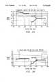
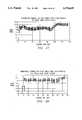
- FIGS. 21 through 26typical process clean endpoint traces are shown in FIGS. 21 through 26. As is apparent from these Figures, one can readily see that shifts in both the fundamental current and current-voltage phase angle signals occur when the deposited chamber 20 films begin to clear. These changes are easily detected by system 80 and can be used to trigger a process termination via programmed endpoint detection process flow as described in FIG. 10.
- FIGS. 27 and 28demonstrate repeatability of the endpoint signal from the present invention. These overlay plots show individual clean endpoint traces over days of production time and are remarkably similar. Changes are seen in the average starting level over time, but the shift in signal level is generally constant. System 80 can be set up to trigger endpoint based on an average level change. Consequently, the starting signal level is not a concern.
- FIG. 29shows the results of obtaining spectral data during a full factorial stress DOX. Wafer measurements were made for comparison.
- FIG. 30shows a representative scan of the radio frequency data from statistical analysis and models were built using radio frequency parameters as input factors and wafer results as output functions. The purpose of this analysis was to predict wafer responses from the in situ radio frequency measurements.
- FIG. 31An excellent linear regression model was obtained for film stress using a subset of the available spectral signals and a similar DOX resulted in a good model for deposited thickness (which is directly applicable to deposition rate).
- the coefficients and ANOVA generated for a linear model of film stressare shown in the t of FIG. 31.
- This modelcan be used to predict wafer results in real time by utilizing radio frequency parameter measurements without the downtime and expense of wafer testing.
- FIGS. 32 and 33graphically demonstrate the relationship between predicted/measured stress and predicted/measured deposition rate, respectively. The confidence intervals are drawn to show that the in situ measurement can accurately forecast the deposition rate and film stress during the deposition process to tight limits. These models could be used to significantly reduce test wafer measurements and therefore cost.
- this demonstrationshows how in situ radio frequency metrology using the present invention can be applied to reduce cost-of-ownership associated with the Applied Materials 5000 PECVD system through improved process control and reduction in wasteful wafer qualification costs. Costs are further reduced by optimizing clean cycles; significantly lowering hardware replacement frequency and reducing PFC gas consumption. Improved process models used to optimize wafer results are likely to result from the application of radio frequency parameter data obtained directly at the powered electrode leading to better process performance and device yields.
- the present inventionprovides a method and system for monitoring the radio frequency power of a plasma in an electronic device fabrication reactor and includes the necessary components and steps of sensing the voltage of the radio frequency power that is directed into a plasma producing gas at the input to the plasma producing environment of the electronic device fabrication reactor.
- the methodsenses also the current and phase angle of the radio frequency power that is directed into the plasma producing gas, also at the input to the plasma producing environment.
- the methodmore completely measures the load that the radio frequency power sees by measuring the full load impedance of the plasma producing environment.
- the full loadin one embodiment, represents not only the discharge and sheath impedances, but also the chuck and wafer impedance, a primary ground path impedance, and a secondary ground path impedance that associates with the plasma environment of the fabrication reactor.
- the methodpermits controlling the plasma environment by accurately measuring voltage, current, and phase associated with the plasma environment.
Landscapes
- Engineering & Computer Science (AREA)
- Chemical & Material Sciences (AREA)
- Physics & Mathematics (AREA)
- Plasma & Fusion (AREA)
- Analytical Chemistry (AREA)
- Mechanical Engineering (AREA)
- Materials Engineering (AREA)
- Chemical Kinetics & Catalysis (AREA)
- General Chemical & Material Sciences (AREA)
- Metallurgy (AREA)
- Organic Chemistry (AREA)
- Manufacturing & Machinery (AREA)
- Computer Hardware Design (AREA)
- Microelectronics & Electronic Packaging (AREA)
- Power Engineering (AREA)
- Plasma Technology (AREA)
- Drying Of Semiconductors (AREA)
Abstract
Description
Claims (43)
Priority Applications (2)
| Application Number | Priority Date | Filing Date | Title |
|---|---|---|---|
| US08/328,069US5576629A (en) | 1994-10-24 | 1994-10-24 | Plasma monitoring and control method and system |
| US08/751,636US5939886A (en) | 1994-10-24 | 1996-11-18 | Plasma monitoring and control method and system |
Applications Claiming Priority (1)
| Application Number | Priority Date | Filing Date | Title |
|---|---|---|---|
| US08/328,069US5576629A (en) | 1994-10-24 | 1994-10-24 | Plasma monitoring and control method and system |
Related Child Applications (1)
| Application Number | Title | Priority Date | Filing Date |
|---|---|---|---|
| US08/751,636DivisionUS5939886A (en) | 1994-10-24 | 1996-11-18 | Plasma monitoring and control method and system |
Publications (1)
| Publication Number | Publication Date |
|---|---|
| US5576629Atrue US5576629A (en) | 1996-11-19 |
Family
ID=23279382
Family Applications (2)
| Application Number | Title | Priority Date | Filing Date |
|---|---|---|---|
| US08/328,069Expired - LifetimeUS5576629A (en) | 1994-10-24 | 1994-10-24 | Plasma monitoring and control method and system |
| US08/751,636Expired - LifetimeUS5939886A (en) | 1994-10-24 | 1996-11-18 | Plasma monitoring and control method and system |
Family Applications After (1)
| Application Number | Title | Priority Date | Filing Date |
|---|---|---|---|
| US08/751,636Expired - LifetimeUS5939886A (en) | 1994-10-24 | 1996-11-18 | Plasma monitoring and control method and system |
Country Status (1)
| Country | Link |
|---|---|
| US (2) | US5576629A (en) |
Cited By (498)
| Publication number | Priority date | Publication date | Assignee | Title |
|---|---|---|---|---|
| US5705931A (en)* | 1994-12-21 | 1998-01-06 | Adolph Slaby Instituut Forschungsgesellschaft Fur Plasmatechnologie Und Mikrostrukturierung Mbh | Method for determining absolute plasma parameters |
| US5844369A (en)* | 1996-05-15 | 1998-12-01 | Daihen Corporation | Automatic phase adjusting circuit for a plasma processing apparatus |
| WO1999029146A1 (en)* | 1997-12-01 | 1999-06-10 | Applied Materials, Inc. | Method and apparatus for monitoring and adjusting chamber impedance |
| US5918144A (en)* | 1996-08-29 | 1999-06-29 | Sony Corporation | Method of manufacturing a semiconductor device |
| US5939886A (en)* | 1994-10-24 | 1999-08-17 | Advanced Energy Industries, Inc. | Plasma monitoring and control method and system |
| US5971591A (en)* | 1997-10-20 | 1999-10-26 | Eni Technologies, Inc. | Process detection system for plasma process |
| US6041734A (en)* | 1997-12-01 | 2000-03-28 | Applied Materials, Inc. | Use of an asymmetric waveform to control ion bombardment during substrate processing |
| US6051284A (en)* | 1996-05-08 | 2000-04-18 | Applied Materials, Inc. | Chamber monitoring and adjustment by plasma RF metrology |
| US6080292A (en)* | 1996-11-19 | 2000-06-27 | Matsuzawa; Reiji | Monitoring apparatus for plasma process |
| US6098568A (en)* | 1997-12-01 | 2000-08-08 | Applied Materials, Inc. | Mixed frequency CVD apparatus |
| US6132552A (en)* | 1998-02-19 | 2000-10-17 | Micron Technology, Inc. | Method and apparatus for controlling the temperature of a gas distribution plate in a process reactor |
| US6197116B1 (en)* | 1996-08-29 | 2001-03-06 | Fujitsu Limited | Plasma processing system |
| US6268226B1 (en)* | 1999-06-30 | 2001-07-31 | International Business Machines Corporation | Reactive ion etch loading measurement technique |
| US6333634B1 (en)* | 1997-09-03 | 2001-12-25 | Mitsubishi Denki Kabushiki Kaisha | Method for measuring radio-frequency current |
| WO2001005197A3 (en)* | 1999-07-13 | 2002-02-14 | Nordson Corp | High-speed symmetrical plasma treatment system |
| US6351683B1 (en) | 1997-09-17 | 2002-02-26 | Tokyo Electron Limited | System and method for monitoring and controlling gas plasma processes |
| US20020040765A1 (en)* | 2000-10-06 | 2002-04-11 | Kawasaki Microelectronics Inc. | Apparatus and methods for processing surface of semiconductor substrate |
| US6406641B1 (en) | 1997-06-17 | 2002-06-18 | Luxtron Corporation | Liquid etch endpoint detection and process metrology |
| US6440260B1 (en)* | 1998-07-10 | 2002-08-27 | Seiko Epson Corporation | Plasma monitoring method and semiconductor production apparatus |
| US6441620B1 (en)* | 2000-06-20 | 2002-08-27 | John Scanlan | Method for fault identification in a plasma process |
| US6449568B1 (en) | 1998-02-27 | 2002-09-10 | Eni Technology, Inc. | Voltage-current sensor with high matching directivity |
| US6447691B1 (en) | 1998-04-07 | 2002-09-10 | Seiko Epson Corporation | Method for detecting end point of plasma etching, and plasma etching apparatus |
| US6455437B1 (en)* | 1999-04-07 | 2002-09-24 | Applied Materials Inc. | Method and apparatus for monitoring the process state of a semiconductor device fabrication process |
| US20020134310A1 (en)* | 2001-03-21 | 2002-09-26 | Condrashoff Robert S. | Material handling system and method for a multi-workpiece plasma treatment system |
| KR20020077648A (en)* | 2001-04-06 | 2002-10-12 | 이엔아이 테크놀로지, 인코포레이티드 | Predictive failure scheme for industrial thin films processing power delivery system |
| US6465263B1 (en)* | 2000-01-04 | 2002-10-15 | Advanced Micro Devices, Inc. | Method and apparatus for implementing corrected species by monitoring specific state parameters |
| US6556884B1 (en)* | 2000-06-16 | 2003-04-29 | Advanced Micro Devices, Inc. | Method and apparatus for interfacing a statistical process control system with a manufacturing process control framework |
| US20030153989A1 (en)* | 2002-02-14 | 2003-08-14 | John Scanlan | Fault classification in a plasma process chamber |
| US6627464B2 (en) | 2001-02-07 | 2003-09-30 | Eni Technology, Inc. | Adaptive plasma characterization system |
| US20030183335A1 (en)* | 1998-09-30 | 2003-10-02 | Winniczek Jaroslaw W. | Methods and apparatus for determining an etch endpoint in a plasma processing system |
| WO2003083911A1 (en)* | 2002-03-28 | 2003-10-09 | Tokyo Electron Limited | A system and method for determining the state of a film in a plasma reactor using an electrical property |
| US20030218427A1 (en)* | 2002-05-22 | 2003-11-27 | Applied Materials, Inc. | Capacitively coupled plasma reactor with magnetic plasma control |
| US20030226821A1 (en)* | 2002-06-07 | 2003-12-11 | Chung-Ho Huang | Integrated stepwise statistical process control in a plasma processing system |
| US20040004708A1 (en)* | 2002-05-29 | 2004-01-08 | Tokyo Electron Limited | Method and system for data handling, storage and manipulation |
| US20040007560A1 (en)* | 2000-07-04 | 2004-01-15 | Shinji Sakano | Method for predicting consumption of consumable part, method for predicting deposited-film thickness, and plasma processor |
| US6685797B2 (en)* | 1999-03-19 | 2004-02-03 | Kabushiki Kaisha Toshiba | Semiconductor device manufacturing system for etching a semiconductor by plasma discharge |
| US6709522B1 (en) | 2000-07-11 | 2004-03-23 | Nordson Corporation | Material handling system and methods for a multichamber plasma treatment system |
| US20040055868A1 (en)* | 2002-09-24 | 2004-03-25 | Scientific Systems Research Limited | Method for fault detection in a plasma process |
| US6727655B2 (en)* | 2001-10-26 | 2004-04-27 | Mcchesney Jon | Method and apparatus to monitor electrical states at a workpiece in a semiconductor processing chamber |
| US6728591B1 (en)* | 2001-08-01 | 2004-04-27 | Advanced Micro Devices, Inc. | Method and apparatus for run-to-run control of trench profiles |
| US20040116080A1 (en)* | 2002-06-24 | 2004-06-17 | Jin-Shyong Chen | Time resolved RF plasma impedance meter |
| US6808592B1 (en) | 1994-12-05 | 2004-10-26 | Nordson Corporation | High throughput plasma treatment system |
| US20040211759A1 (en)* | 2000-03-17 | 2004-10-28 | Applied Materials, Inc. | Merie plasma reactor with overhead RF electrode tuned to the plasma with arcing suppression |
| US6815633B1 (en) | 1997-06-26 | 2004-11-09 | Applied Science & Technology, Inc. | Inductively-coupled toroidal plasma source |
| US20040226657A1 (en)* | 2003-05-16 | 2004-11-18 | Applied Materials, Inc. | Plasma density, energy and etch rate measurements at bias power input and real time feedback control of plasma source and bias power |
| US20040235304A1 (en)* | 2001-12-27 | 2004-11-25 | Tokyo Electron Limited | Plasma treatment apparatus |
| US6842658B2 (en)* | 2001-02-01 | 2005-01-11 | Hitachi, Ltd. | Method of manufacturing a semiconductor device and manufacturing system |
| US6853953B2 (en) | 2001-08-07 | 2005-02-08 | Tokyo Electron Limited | Method for characterizing the performance of an electrostatic chuck |
| US20050038543A1 (en)* | 2003-08-13 | 2005-02-17 | Shui-Tien Lin | Method and system for synchronizing control limit and equipment performance |
| US20050057164A1 (en)* | 2002-05-31 | 2005-03-17 | Toshiaki Kitamura | Coaxial type impedance matching device and impedance detecting method for plasma generation |
| US6871112B1 (en)* | 2000-01-07 | 2005-03-22 | Advanced Micro Devices, Inc. | Method for requesting trace data reports from FDC semiconductor fabrication processes |
| US20050067102A1 (en)* | 2003-09-30 | 2005-03-31 | Baldwin Craig T. | Method and apparatus for detecting a plasma |
| US6924455B1 (en) | 1997-06-26 | 2005-08-02 | Applied Science & Technology, Inc. | Integrated plasma chamber and inductively-coupled toroidal plasma source |
| US20050167396A1 (en)* | 2004-02-02 | 2005-08-04 | International Business Machines Corporation | A measurement to determine plasma leakage |
| US20050183821A1 (en)* | 2002-07-03 | 2005-08-25 | Tokyo Electron Limited | Method and apparatus for non-invasive measurement and analysis of semiconductor process parameters |
| US20050194094A1 (en)* | 2002-04-24 | 2005-09-08 | Mitsuo Yasaka | Window type probe, plasma monitoring device, and plasma processing device |
| US20050217795A1 (en)* | 2004-03-30 | 2005-10-06 | Armen Avoyan | Method of plasma etch endpoint detection using a V-I probe diagnostics |
| US6970700B1 (en)* | 2000-01-31 | 2005-11-29 | Eni Technology, Inc. | Power delivery system |
| US6972071B1 (en) | 1999-07-13 | 2005-12-06 | Nordson Corporation | High-speed symmetrical plasma treatment system |
| US20060005928A1 (en)* | 2002-03-08 | 2006-01-12 | Lam Research Corporation | Apparatus and methods for improving the stability of RF power delivery to a plasma load |
| US20060021970A1 (en)* | 2002-07-03 | 2006-02-02 | Tokyo Electron Limited | Method and apparatus for non-invasive measurement and analysis of semiconductor process parameters |
| US20060074590A1 (en)* | 2004-09-27 | 2006-04-06 | Bailey Andrew Iii | Computer-implemented data presentation techniques for a plasma processing system |
| US7030335B2 (en) | 2000-03-17 | 2006-04-18 | Applied Materials, Inc. | Plasma reactor with overhead RF electrode tuned to the plasma with arcing suppression |
| US20060170367A1 (en)* | 2005-01-11 | 2006-08-03 | Bhutta Imran A | Method of detecting RF power delivered to a load and complex impedance of the load |
| US7141757B2 (en) | 2000-03-17 | 2006-11-28 | Applied Materials, Inc. | Plasma reactor with overhead RF source power electrode having a resonance that is virtually pressure independent |
| US7161112B2 (en) | 1997-06-26 | 2007-01-09 | Mks Instruments, Inc. | Toroidal low-field reactive gas source |
| US7166816B1 (en) | 1997-06-26 | 2007-01-23 | Mks Instruments, Inc. | Inductively-coupled torodial plasma source |
| US7196283B2 (en) | 2000-03-17 | 2007-03-27 | Applied Materials, Inc. | Plasma reactor overhead source power electrode with low arcing tendency, cylindrical gas outlets and shaped surface |
| US7220937B2 (en) | 2000-03-17 | 2007-05-22 | Applied Materials, Inc. | Plasma reactor with overhead RF source power electrode with low loss, low arcing tendency and low contamination |
| US20070193976A1 (en)* | 2006-02-22 | 2007-08-23 | Hitoshi Tamura | Plasma processing apparatus and plasma processing method |
| US20080029385A1 (en)* | 2006-08-03 | 2008-02-07 | Tokyo Electron Limited | Plasma processing apparatus and plasma processing method |
| US7359177B2 (en) | 2005-05-10 | 2008-04-15 | Applied Materials, Inc. | Dual bias frequency plasma reactor with feedback control of E.S.C. voltage using wafer voltage measurement at the bias supply output |
| US20080258836A1 (en)* | 2007-04-19 | 2008-10-23 | Kim Jae-Hyun | Impedance matching methods and systems performing the same |
| US20080270048A1 (en)* | 2007-04-26 | 2008-10-30 | Van Zyl Gideon | Method and apparatus for modifying interactions between an electrical generator and a nonlinear load |
| US7452824B2 (en) | 2003-05-16 | 2008-11-18 | Applied Materials, Inc. | Method of characterizing a chamber based upon concurrent behavior of selected plasma parameters as a function of plural chamber parameters |
| US7470626B2 (en) | 2003-05-16 | 2008-12-30 | Applied Materials, Inc. | Method of characterizing a chamber based upon concurrent behavior of selected plasma parameters as a function of source power, bias power and chamber pressure |
| WO2009114791A1 (en)* | 2008-03-14 | 2009-09-17 | Forth-Rite Technologies, Inc. | Effluent impedance based endpoint detection |
| US20090281741A1 (en)* | 2008-05-07 | 2009-11-12 | Van Zyl Gideon J | System, method, and apparatus for monitoring power |
| US7695984B1 (en) | 2005-04-20 | 2010-04-13 | Pivotal Systems Corporation | Use of modeled parameters for real-time semiconductor process metrology applied to semiconductor processes |
| US20100174420A1 (en)* | 2008-12-31 | 2010-07-08 | Van Zyl Gideon | Method and apparatus for adjusting the reference impedance of a power generator |
| US7795153B2 (en) | 2003-05-16 | 2010-09-14 | Applied Materials, Inc. | Method of controlling a chamber based upon predetermined concurrent behavior of selected plasma parameters as a function of selected chamber parameters |
| EP2228818A2 (en) | 2009-03-10 | 2010-09-15 | Schott AG | Method for monitoring plasma discharges |
| US7901952B2 (en) | 2003-05-16 | 2011-03-08 | Applied Materials, Inc. | Plasma reactor control by translating desired values of M plasma parameters to values of N chamber parameters |
| US20110060442A1 (en)* | 2009-09-10 | 2011-03-10 | Valcore Jr John C | Methods and arrangement for detecting a wafer-released event within a plasma processing chamber |
| US20110058302A1 (en)* | 2009-09-10 | 2011-03-10 | Valcore Jr John C | Methods and arrangement for plasma dechuck optimization based on coupling of plasma signaling to substrate position and potential |
| US7910013B2 (en) | 2003-05-16 | 2011-03-22 | Applied Materials, Inc. | Method of controlling a chamber based upon predetermined concurrent behavior of selected plasma parameters as a function of source power, bias power and chamber pressure |
| US7955986B2 (en) | 2002-05-22 | 2011-06-07 | Applied Materials, Inc. | Capacitively coupled plasma reactor with magnetic plasma control |
| US8048806B2 (en) | 2000-03-17 | 2011-11-01 | Applied Materials, Inc. | Methods to avoid unstable plasma states during a process transition |
| US8124906B2 (en) | 1997-06-26 | 2012-02-28 | Mks Instruments, Inc. | Method and apparatus for processing metal bearing gases |
| US20120212135A1 (en)* | 2011-02-23 | 2012-08-23 | Kabushiki Kaisha Toshiba | Control apparatus, plasma processing apparatus, method for controlling control apparatus |
| US20120227903A1 (en)* | 2006-04-27 | 2012-09-13 | Applied Materials, Inc. | Automatic Gain Control |
| CN102822380A (en)* | 2010-04-02 | 2012-12-12 | 株式会社爱发科 | Sputtering apparatus and sputtering method |
| US8617351B2 (en) | 2002-07-09 | 2013-12-31 | Applied Materials, Inc. | Plasma reactor with minimal D.C. coils for cusp, solenoid and mirror fields for plasma uniformity and device damage reduction |
| US8716984B2 (en) | 2009-06-29 | 2014-05-06 | Advanced Energy Industries, Inc. | Method and apparatus for modifying the sensitivity of an electrical generator to a nonlinear load |
| US20140152189A1 (en)* | 2012-06-15 | 2014-06-05 | COMET Technologies USA, Inc. | Plasma pulse tracking system and method |
| US8779322B2 (en) | 1997-06-26 | 2014-07-15 | Mks Instruments Inc. | Method and apparatus for processing metal bearing gases |
| US20140265910A1 (en)* | 2013-03-13 | 2014-09-18 | Applied Materials, Inc. | Digital phase controller for two-phase operation of a plasma reactor |
| US20140346650A1 (en)* | 2009-08-14 | 2014-11-27 | Asm Ip Holding B.V. | Systems and methods for thin-film deposition of metal oxides using excited nitrogen-oxygen species |
| US20150047974A1 (en)* | 2012-03-26 | 2015-02-19 | Tokyo Electron Limited | Plasma processing apparatus and high frequency generator |
| CN104425208A (en)* | 2013-09-11 | 2015-03-18 | 北京北方微电子基地设备工艺研究中心有限责任公司 | Impedance matching method |
| CN104934340A (en)* | 2014-03-21 | 2015-09-23 | 北京北方微电子基地设备工艺研究中心有限责任公司 | Radio frequency sensor and impedance matching device |
| US20160216100A1 (en)* | 2015-01-22 | 2016-07-28 | Samsung Display Co., Ltd. | Apparatus for measuring contamination of plasma generating device |
| US20170062186A1 (en)* | 2015-08-27 | 2017-03-02 | Mks Instruments, Inc. | Feedback Control By RF Waveform Tailoring for Ion Energy Distribution |
| US9745660B2 (en) | 2014-05-02 | 2017-08-29 | Reno Technologies, Inc. | Method for controlling a plasma chamber |
| US9859151B1 (en) | 2016-07-08 | 2018-01-02 | Asm Ip Holding B.V. | Selective film deposition method to form air gaps |
| US9887082B1 (en) | 2016-07-28 | 2018-02-06 | Asm Ip Holding B.V. | Method and apparatus for filling a gap |
| US9916980B1 (en) | 2016-12-15 | 2018-03-13 | Asm Ip Holding B.V. | Method of forming a structure on a substrate |
| US10023960B2 (en) | 2012-09-12 | 2018-07-17 | Asm Ip Holdings B.V. | Process gas management for an inductively-coupled plasma deposition reactor |
| US10026592B2 (en) | 2016-07-01 | 2018-07-17 | Lam Research Corporation | Systems and methods for tailoring ion energy distribution function by odd harmonic mixing |
| US10083836B2 (en) | 2015-07-24 | 2018-09-25 | Asm Ip Holding B.V. | Formation of boron-doped titanium metal films with high work function |
| US10087522B2 (en) | 2016-04-21 | 2018-10-02 | Asm Ip Holding B.V. | Deposition of metal borides |
| US10103040B1 (en) | 2017-03-31 | 2018-10-16 | Asm Ip Holding B.V. | Apparatus and method for manufacturing a semiconductor device |
| KR20180116225A (en)* | 2016-01-22 | 2018-10-24 | 에스피피 테크놀로지스 컴퍼니 리미티드 | Plasma control device |
| US10134757B2 (en) | 2016-11-07 | 2018-11-20 | Asm Ip Holding B.V. | Method of processing a substrate and a device manufactured by using the method |
| US20180366306A1 (en)* | 2015-06-17 | 2018-12-20 | Applied Materials, Inc. | Multiple electrode substrate support assembly and phase control system |
| US10177025B2 (en) | 2016-07-28 | 2019-01-08 | Asm Ip Holding B.V. | Method and apparatus for filling a gap |
| US10229833B2 (en) | 2016-11-01 | 2019-03-12 | Asm Ip Holding B.V. | Methods for forming a transition metal nitride film on a substrate by atomic layer deposition and related semiconductor device structures |
| US10236177B1 (en) | 2017-08-22 | 2019-03-19 | ASM IP Holding B.V.. | Methods for depositing a doped germanium tin semiconductor and related semiconductor device structures |
| US10249577B2 (en) | 2016-05-17 | 2019-04-02 | Asm Ip Holding B.V. | Method of forming metal interconnection and method of fabricating semiconductor apparatus using the method |
| US10249524B2 (en) | 2017-08-09 | 2019-04-02 | Asm Ip Holding B.V. | Cassette holder assembly for a substrate cassette and holding member for use in such assembly |
| US10262859B2 (en) | 2016-03-24 | 2019-04-16 | Asm Ip Holding B.V. | Process for forming a film on a substrate using multi-port injection assemblies |
| US10269558B2 (en) | 2016-12-22 | 2019-04-23 | Asm Ip Holding B.V. | Method of forming a structure on a substrate |
| US10276355B2 (en) | 2015-03-12 | 2019-04-30 | Asm Ip Holding B.V. | Multi-zone reactor, system including the reactor, and method of using the same |
| US10283353B2 (en) | 2017-03-29 | 2019-05-07 | Asm Ip Holding B.V. | Method of reforming insulating film deposited on substrate with recess pattern |
| US10290508B1 (en) | 2017-12-05 | 2019-05-14 | Asm Ip Holding B.V. | Method for forming vertical spacers for spacer-defined patterning |
| US10312055B2 (en) | 2017-07-26 | 2019-06-04 | Asm Ip Holding B.V. | Method of depositing film by PEALD using negative bias |
| US10312129B2 (en) | 2015-09-29 | 2019-06-04 | Asm Ip Holding B.V. | Variable adjustment for precise matching of multiple chamber cavity housings |
| US10319588B2 (en) | 2017-10-10 | 2019-06-11 | Asm Ip Holding B.V. | Method for depositing a metal chalcogenide on a substrate by cyclical deposition |
| US10322384B2 (en) | 2015-11-09 | 2019-06-18 | Asm Ip Holding B.V. | Counter flow mixer for process chamber |
| US10340125B2 (en) | 2013-03-08 | 2019-07-02 | Asm Ip Holding B.V. | Pulsed remote plasma method and system |
| US10340135B2 (en) | 2016-11-28 | 2019-07-02 | Asm Ip Holding B.V. | Method of topologically restricted plasma-enhanced cyclic deposition of silicon or metal nitride |
| US10343920B2 (en) | 2016-03-18 | 2019-07-09 | Asm Ip Holding B.V. | Aligned carbon nanotubes |
| US10361201B2 (en) | 2013-09-27 | 2019-07-23 | Asm Ip Holding B.V. | Semiconductor structure and device formed using selective epitaxial process |
| US10364496B2 (en) | 2011-06-27 | 2019-07-30 | Asm Ip Holding B.V. | Dual section module having shared and unshared mass flow controllers |
| US10367080B2 (en) | 2016-05-02 | 2019-07-30 | Asm Ip Holding B.V. | Method of forming a germanium oxynitride film |
| US10366864B2 (en) | 2013-03-08 | 2019-07-30 | Asm Ip Holding B.V. | Method and system for in-situ formation of intermediate reactive species |
| US20190237305A1 (en)* | 2018-01-26 | 2019-08-01 | Tokyo Electron Limited | Method for applying dc voltage and plasma processing apparatus |
| US10378106B2 (en) | 2008-11-14 | 2019-08-13 | Asm Ip Holding B.V. | Method of forming insulation film by modified PEALD |
| US10381219B1 (en) | 2018-10-25 | 2019-08-13 | Asm Ip Holding B.V. | Methods for forming a silicon nitride film |
| US10381226B2 (en) | 2016-07-27 | 2019-08-13 | Asm Ip Holding B.V. | Method of processing substrate |
| US10388513B1 (en) | 2018-07-03 | 2019-08-20 | Asm Ip Holding B.V. | Method for depositing silicon-free carbon-containing film as gap-fill layer by pulse plasma-assisted deposition |
| US10388509B2 (en) | 2016-06-28 | 2019-08-20 | Asm Ip Holding B.V. | Formation of epitaxial layers via dislocation filtering |
| US10395919B2 (en) | 2016-07-28 | 2019-08-27 | Asm Ip Holding B.V. | Method and apparatus for filling a gap |
| US10403504B2 (en) | 2017-10-05 | 2019-09-03 | Asm Ip Holding B.V. | Method for selectively depositing a metallic film on a substrate |
| US10410943B2 (en) | 2016-10-13 | 2019-09-10 | Asm Ip Holding B.V. | Method for passivating a surface of a semiconductor and related systems |
| US10431428B2 (en) | 2014-01-10 | 2019-10-01 | Reno Technologies, Inc. | System for providing variable capacitance |
| US10438965B2 (en) | 2014-12-22 | 2019-10-08 | Asm Ip Holding B.V. | Semiconductor device and manufacturing method thereof |
| US10435790B2 (en) | 2016-11-01 | 2019-10-08 | Asm Ip Holding B.V. | Method of subatmospheric plasma-enhanced ALD using capacitively coupled electrodes with narrow gap |
| US10446393B2 (en) | 2017-05-08 | 2019-10-15 | Asm Ip Holding B.V. | Methods for forming silicon-containing epitaxial layers and related semiconductor device structures |
| US10458018B2 (en) | 2015-06-26 | 2019-10-29 | Asm Ip Holding B.V. | Structures including metal carbide material, devices including the structures, and methods of forming same |
| US10468261B2 (en) | 2017-02-15 | 2019-11-05 | Asm Ip Holding B.V. | Methods for forming a metallic film on a substrate by cyclical deposition and related semiconductor device structures |
| US10468251B2 (en) | 2016-02-19 | 2019-11-05 | Asm Ip Holding B.V. | Method for forming spacers using silicon nitride film for spacer-defined multiple patterning |
| US10480072B2 (en) | 2009-04-06 | 2019-11-19 | Asm Ip Holding B.V. | Semiconductor processing reactor and components thereof |
| US10483099B1 (en) | 2018-07-26 | 2019-11-19 | Asm Ip Holding B.V. | Method for forming thermally stable organosilicon polymer film |
| US10501866B2 (en) | 2016-03-09 | 2019-12-10 | Asm Ip Holding B.V. | Gas distribution apparatus for improved film uniformity in an epitaxial system |
| US10504742B2 (en) | 2017-05-31 | 2019-12-10 | Asm Ip Holding B.V. | Method of atomic layer etching using hydrogen plasma |
| US10510536B2 (en) | 2018-03-29 | 2019-12-17 | Asm Ip Holding B.V. | Method of depositing a co-doped polysilicon film on a surface of a substrate within a reaction chamber |
| US10529563B2 (en) | 2017-03-29 | 2020-01-07 | Asm Ip Holdings B.V. | Method for forming doped metal oxide films on a substrate by cyclical deposition and related semiconductor device structures |
| US10529554B2 (en) | 2016-02-19 | 2020-01-07 | Asm Ip Holding B.V. | Method for forming silicon nitride film selectively on sidewalls or flat surfaces of trenches |
| US10529542B2 (en) | 2015-03-11 | 2020-01-07 | Asm Ip Holdings B.V. | Cross-flow reactor and method |
| US10535516B2 (en) | 2018-02-01 | 2020-01-14 | Asm Ip Holdings B.V. | Method for depositing a semiconductor structure on a surface of a substrate and related semiconductor structures |
| US10541333B2 (en) | 2017-07-19 | 2020-01-21 | Asm Ip Holding B.V. | Method for depositing a group IV semiconductor and related semiconductor device structures |
| US10559458B1 (en) | 2018-11-26 | 2020-02-11 | Asm Ip Holding B.V. | Method of forming oxynitride film |
| KR20200015841A (en)* | 2017-07-13 | 2020-02-12 | 어플라이드 머티어리얼스, 인코포레이티드 | Substrate Processing Method and Apparatus |
| US10561975B2 (en) | 2014-10-07 | 2020-02-18 | Asm Ip Holdings B.V. | Variable conductance gas distribution apparatus and method |
| US10566223B2 (en) | 2012-08-28 | 2020-02-18 | Asm Ip Holdings B.V. | Systems and methods for dynamic semiconductor process scheduling |
| US10590535B2 (en) | 2017-07-26 | 2020-03-17 | Asm Ip Holdings B.V. | Chemical treatment, deposition and/or infiltration apparatus and method for using the same |
| US10600673B2 (en) | 2015-07-07 | 2020-03-24 | Asm Ip Holding B.V. | Magnetic susceptor to baseplate seal |
| US10607895B2 (en) | 2017-09-18 | 2020-03-31 | Asm Ip Holdings B.V. | Method for forming a semiconductor device structure comprising a gate fill metal |
| US10605530B2 (en) | 2017-07-26 | 2020-03-31 | Asm Ip Holding B.V. | Assembly of a liner and a flange for a vertical furnace as well as the liner and the vertical furnace |
| US10604847B2 (en) | 2014-03-18 | 2020-03-31 | Asm Ip Holding B.V. | Gas distribution system, reactor including the system, and methods of using the same |
| US10612136B2 (en) | 2018-06-29 | 2020-04-07 | ASM IP Holding, B.V. | Temperature-controlled flange and reactor system including same |
| US10612137B2 (en) | 2016-07-08 | 2020-04-07 | Asm Ip Holdings B.V. | Organic reactants for atomic layer deposition |
| USD880437S1 (en) | 2018-02-01 | 2020-04-07 | Asm Ip Holding B.V. | Gas supply plate for semiconductor manufacturing apparatus |
| US10643826B2 (en) | 2016-10-26 | 2020-05-05 | Asm Ip Holdings B.V. | Methods for thermally calibrating reaction chambers |
| US10643904B2 (en) | 2016-11-01 | 2020-05-05 | Asm Ip Holdings B.V. | Methods for forming a semiconductor device and related semiconductor device structures |
| US10655221B2 (en) | 2017-02-09 | 2020-05-19 | Asm Ip Holding B.V. | Method for depositing oxide film by thermal ALD and PEALD |
| US10658205B2 (en) | 2017-09-28 | 2020-05-19 | Asm Ip Holdings B.V. | Chemical dispensing apparatus and methods for dispensing a chemical to a reaction chamber |
| US10658181B2 (en) | 2018-02-20 | 2020-05-19 | Asm Ip Holding B.V. | Method of spacer-defined direct patterning in semiconductor fabrication |
| US10665452B2 (en) | 2016-05-02 | 2020-05-26 | Asm Ip Holdings B.V. | Source/drain performance through conformal solid state doping |
| US10685834B2 (en) | 2017-07-05 | 2020-06-16 | Asm Ip Holdings B.V. | Methods for forming a silicon germanium tin layer and related semiconductor device structures |
| US10683571B2 (en) | 2014-02-25 | 2020-06-16 | Asm Ip Holding B.V. | Gas supply manifold and method of supplying gases to chamber using same |
| US10692741B2 (en) | 2017-08-08 | 2020-06-23 | Asm Ip Holdings B.V. | Radiation shield |
| US10707106B2 (en) | 2011-06-06 | 2020-07-07 | Asm Ip Holding B.V. | High-throughput semiconductor-processing apparatus equipped with multiple dual-chamber modules |
| US10714385B2 (en) | 2016-07-19 | 2020-07-14 | Asm Ip Holding B.V. | Selective deposition of tungsten |
| US10714350B2 (en) | 2016-11-01 | 2020-07-14 | ASM IP Holdings, B.V. | Methods for forming a transition metal niobium nitride film on a substrate by atomic layer deposition and related semiconductor device structures |
| US10714315B2 (en) | 2012-10-12 | 2020-07-14 | Asm Ip Holdings B.V. | Semiconductor reaction chamber showerhead |
| US10714335B2 (en) | 2017-04-25 | 2020-07-14 | Asm Ip Holding B.V. | Method of depositing thin film and method of manufacturing semiconductor device |
| US10734244B2 (en) | 2017-11-16 | 2020-08-04 | Asm Ip Holding B.V. | Method of processing a substrate and a device manufactured by the same |
| US10734497B2 (en) | 2017-07-18 | 2020-08-04 | Asm Ip Holding B.V. | Methods for forming a semiconductor device structure and related semiconductor device structures |
| US10731249B2 (en) | 2018-02-15 | 2020-08-04 | Asm Ip Holding B.V. | Method of forming a transition metal containing film on a substrate by a cyclical deposition process, a method for supplying a transition metal halide compound to a reaction chamber, and related vapor deposition apparatus |
| US10748797B2 (en) | 2017-01-18 | 2020-08-18 | Applied Materials, Inc. | Plasma parameters and skew characterization by high speed imaging |
| US10755922B2 (en) | 2018-07-03 | 2020-08-25 | Asm Ip Holding B.V. | Method for depositing silicon-free carbon-containing film as gap-fill layer by pulse plasma-assisted deposition |
| CN111600307A (en)* | 2020-06-01 | 2020-08-28 | 中国科学院微电子研究所 | Harmonic monitoring system and monitoring method of radio frequency power supply, semiconductor equipment system |
| US10770336B2 (en) | 2017-08-08 | 2020-09-08 | Asm Ip Holding B.V. | Substrate lift mechanism and reactor including same |
| US10770286B2 (en) | 2017-05-08 | 2020-09-08 | Asm Ip Holdings B.V. | Methods for selectively forming a silicon nitride film on a substrate and related semiconductor device structures |
| US10767789B2 (en) | 2018-07-16 | 2020-09-08 | Asm Ip Holding B.V. | Diaphragm valves, valve components, and methods for forming valve components |
| US10787741B2 (en) | 2014-08-21 | 2020-09-29 | Asm Ip Holding B.V. | Method and system for in situ formation of gas-phase compounds |
| US10797133B2 (en) | 2018-06-21 | 2020-10-06 | Asm Ip Holding B.V. | Method for depositing a phosphorus doped silicon arsenide film and related semiconductor device structures |
| US10811256B2 (en) | 2018-10-16 | 2020-10-20 | Asm Ip Holding B.V. | Method for etching a carbon-containing feature |
| US10818758B2 (en) | 2018-11-16 | 2020-10-27 | Asm Ip Holding B.V. | Methods for forming a metal silicate film on a substrate in a reaction chamber and related semiconductor device structures |
| USD900036S1 (en) | 2017-08-24 | 2020-10-27 | Asm Ip Holding B.V. | Heater electrical connector and adapter |
| US10832903B2 (en) | 2011-10-28 | 2020-11-10 | Asm Ip Holding B.V. | Process feed management for semiconductor substrate processing |
| US10829852B2 (en) | 2018-08-16 | 2020-11-10 | Asm Ip Holding B.V. | Gas distribution device for a wafer processing apparatus |
| US10844484B2 (en) | 2017-09-22 | 2020-11-24 | Asm Ip Holding B.V. | Apparatus for dispensing a vapor phase reactant to a reaction chamber and related methods |
| US10847366B2 (en) | 2018-11-16 | 2020-11-24 | Asm Ip Holding B.V. | Methods for depositing a transition metal chalcogenide film on a substrate by a cyclical deposition process |
| US10847371B2 (en) | 2018-03-27 | 2020-11-24 | Asm Ip Holding B.V. | Method of forming an electrode on a substrate and a semiconductor device structure including an electrode |
| US10847365B2 (en) | 2018-10-11 | 2020-11-24 | Asm Ip Holding B.V. | Method of forming conformal silicon carbide film by cyclic CVD |
| USD903477S1 (en) | 2018-01-24 | 2020-12-01 | Asm Ip Holdings B.V. | Metal clamp |
| US10851456B2 (en) | 2016-04-21 | 2020-12-01 | Asm Ip Holding B.V. | Deposition of metal borides |
| US10854498B2 (en) | 2011-07-15 | 2020-12-01 | Asm Ip Holding B.V. | Wafer-supporting device and method for producing same |
| US10858737B2 (en) | 2014-07-28 | 2020-12-08 | Asm Ip Holding B.V. | Showerhead assembly and components thereof |
| US10865475B2 (en) | 2016-04-21 | 2020-12-15 | Asm Ip Holding B.V. | Deposition of metal borides and silicides |
| US10867788B2 (en) | 2016-12-28 | 2020-12-15 | Asm Ip Holding B.V. | Method of forming a structure on a substrate |
| US10867786B2 (en) | 2018-03-30 | 2020-12-15 | Asm Ip Holding B.V. | Substrate processing method |
| US10872771B2 (en) | 2018-01-16 | 2020-12-22 | Asm Ip Holding B. V. | Method for depositing a material film on a substrate within a reaction chamber by a cyclical deposition process and related device structures |
| US10886123B2 (en) | 2017-06-02 | 2021-01-05 | Asm Ip Holding B.V. | Methods for forming low temperature semiconductor layers and related semiconductor device structures |
| US10883175B2 (en) | 2018-08-09 | 2021-01-05 | Asm Ip Holding B.V. | Vertical furnace for processing substrates and a liner for use therein |
| US10892156B2 (en) | 2017-05-08 | 2021-01-12 | Asm Ip Holding B.V. | Methods for forming a silicon nitride film on a substrate and related semiconductor device structures |
| US10896820B2 (en) | 2018-02-14 | 2021-01-19 | Asm Ip Holding B.V. | Method for depositing a ruthenium-containing film on a substrate by a cyclical deposition process |
| US10910262B2 (en) | 2017-11-16 | 2021-02-02 | Asm Ip Holding B.V. | Method of selectively depositing a capping layer structure on a semiconductor device structure |
| US10914004B2 (en) | 2018-06-29 | 2021-02-09 | Asm Ip Holding B.V. | Thin-film deposition method and manufacturing method of semiconductor device |
| US10923344B2 (en) | 2017-10-30 | 2021-02-16 | Asm Ip Holding B.V. | Methods for forming a semiconductor structure and related semiconductor structures |
| US10928731B2 (en) | 2017-09-21 | 2021-02-23 | Asm Ip Holding B.V. | Method of sequential infiltration synthesis treatment of infiltrateable material and structures and devices formed using same |
| US10934619B2 (en) | 2016-11-15 | 2021-03-02 | Asm Ip Holding B.V. | Gas supply unit and substrate processing apparatus including the gas supply unit |
| US10941490B2 (en) | 2014-10-07 | 2021-03-09 | Asm Ip Holding B.V. | Multiple temperature range susceptor, assembly, reactor and system including the susceptor, and methods of using the same |
| US10975470B2 (en) | 2018-02-23 | 2021-04-13 | Asm Ip Holding B.V. | Apparatus for detecting or monitoring for a chemical precursor in a high temperature environment |
| US11001925B2 (en) | 2016-12-19 | 2021-05-11 | Asm Ip Holding B.V. | Substrate processing apparatus |
| US11018002B2 (en) | 2017-07-19 | 2021-05-25 | Asm Ip Holding B.V. | Method for selectively depositing a Group IV semiconductor and related semiconductor device structures |
| US11018047B2 (en) | 2018-01-25 | 2021-05-25 | Asm Ip Holding B.V. | Hybrid lift pin |
| US11015245B2 (en) | 2014-03-19 | 2021-05-25 | Asm Ip Holding B.V. | Gas-phase reactor and system having exhaust plenum and components thereof |
| US11022879B2 (en) | 2017-11-24 | 2021-06-01 | Asm Ip Holding B.V. | Method of forming an enhanced unexposed photoresist layer |
| US11024523B2 (en) | 2018-09-11 | 2021-06-01 | Asm Ip Holding B.V. | Substrate processing apparatus and method |
| US11031242B2 (en) | 2018-11-07 | 2021-06-08 | Asm Ip Holding B.V. | Methods for depositing a boron doped silicon germanium film |
| USD922229S1 (en) | 2019-06-05 | 2021-06-15 | Asm Ip Holding B.V. | Device for controlling a temperature of a gas supply unit |
| US11049751B2 (en) | 2018-09-14 | 2021-06-29 | Asm Ip Holding B.V. | Cassette supply system to store and handle cassettes and processing apparatus equipped therewith |
| US11056567B2 (en) | 2018-05-11 | 2021-07-06 | Asm Ip Holding B.V. | Method of forming a doped metal carbide film on a substrate and related semiconductor device structures |
| US11056344B2 (en) | 2017-08-30 | 2021-07-06 | Asm Ip Holding B.V. | Layer forming method |
| US11053591B2 (en) | 2018-08-06 | 2021-07-06 | Asm Ip Holding B.V. | Multi-port gas injection system and reactor system including same |
| US11069510B2 (en) | 2017-08-30 | 2021-07-20 | Asm Ip Holding B.V. | Substrate processing apparatus |
| US11081345B2 (en) | 2018-02-06 | 2021-08-03 | Asm Ip Holding B.V. | Method of post-deposition treatment for silicon oxide film |
| US11087997B2 (en) | 2018-10-31 | 2021-08-10 | Asm Ip Holding B.V. | Substrate processing apparatus for processing substrates |
| US11088002B2 (en) | 2018-03-29 | 2021-08-10 | Asm Ip Holding B.V. | Substrate rack and a substrate processing system and method |
| US11107661B2 (en) | 2019-07-09 | 2021-08-31 | COMET Technologies USA, Inc. | Hybrid matching network topology |
| US11114279B2 (en) | 2019-06-28 | 2021-09-07 | COMET Technologies USA, Inc. | Arc suppression device for plasma processing equipment |
| US11114283B2 (en) | 2018-03-16 | 2021-09-07 | Asm Ip Holding B.V. | Reactor, system including the reactor, and methods of manufacturing and using same |
| US11114294B2 (en) | 2019-03-08 | 2021-09-07 | Asm Ip Holding B.V. | Structure including SiOC layer and method of forming same |
| USD930782S1 (en) | 2019-08-22 | 2021-09-14 | Asm Ip Holding B.V. | Gas distributor |
| US11127617B2 (en) | 2017-11-27 | 2021-09-21 | Asm Ip Holding B.V. | Storage device for storing wafer cassettes for use with a batch furnace |
| US11127589B2 (en) | 2019-02-01 | 2021-09-21 | Asm Ip Holding B.V. | Method of topology-selective film formation of silicon oxide |
| USD931978S1 (en) | 2019-06-27 | 2021-09-28 | Asm Ip Holding B.V. | Showerhead vacuum transport |
| US11139308B2 (en) | 2015-12-29 | 2021-10-05 | Asm Ip Holding B.V. | Atomic layer deposition of III-V compounds to form V-NAND devices |
| US11139191B2 (en) | 2017-08-09 | 2021-10-05 | Asm Ip Holding B.V. | Storage apparatus for storing cassettes for substrates and processing apparatus equipped therewith |
| US11158513B2 (en) | 2018-12-13 | 2021-10-26 | Asm Ip Holding B.V. | Methods for forming a rhenium-containing film on a substrate by a cyclical deposition process and related semiconductor device structures |
| USD935572S1 (en) | 2019-05-24 | 2021-11-09 | Asm Ip Holding B.V. | Gas channel plate |
| US11171025B2 (en) | 2019-01-22 | 2021-11-09 | Asm Ip Holding B.V. | Substrate processing device |
| US11205585B2 (en) | 2016-07-28 | 2021-12-21 | Asm Ip Holding B.V. | Substrate processing apparatus and method of operating the same |
| US11217444B2 (en) | 2018-11-30 | 2022-01-04 | Asm Ip Holding B.V. | Method for forming an ultraviolet radiation responsive metal oxide-containing film |
| US11222772B2 (en) | 2016-12-14 | 2022-01-11 | Asm Ip Holding B.V. | Substrate processing apparatus |
| USD940837S1 (en) | 2019-08-22 | 2022-01-11 | Asm Ip Holding B.V. | Electrode |
| US11227782B2 (en) | 2019-07-31 | 2022-01-18 | Asm Ip Holding B.V. | Vertical batch furnace assembly |
| US11227789B2 (en) | 2019-02-20 | 2022-01-18 | Asm Ip Holding B.V. | Method and apparatus for filling a recess formed within a substrate surface |
| US11233133B2 (en) | 2015-10-21 | 2022-01-25 | Asm Ip Holding B.V. | NbMC layers |
| US11230766B2 (en) | 2018-03-29 | 2022-01-25 | Asm Ip Holding B.V. | Substrate processing apparatus and method |
| US11232963B2 (en) | 2018-10-03 | 2022-01-25 | Asm Ip Holding B.V. | Substrate processing apparatus and method |
| US11251068B2 (en) | 2018-10-19 | 2022-02-15 | Asm Ip Holding B.V. | Substrate processing apparatus and substrate processing method |
| US11251040B2 (en) | 2019-02-20 | 2022-02-15 | Asm Ip Holding B.V. | Cyclical deposition method including treatment step and apparatus for same |
| USD944946S1 (en) | 2019-06-14 | 2022-03-01 | Asm Ip Holding B.V. | Shower plate |
| US11270899B2 (en) | 2018-06-04 | 2022-03-08 | Asm Ip Holding B.V. | Wafer handling chamber with moisture reduction |
| US11274369B2 (en) | 2018-09-11 | 2022-03-15 | Asm Ip Holding B.V. | Thin film deposition method |
| US11282698B2 (en) | 2019-07-19 | 2022-03-22 | Asm Ip Holding B.V. | Method of forming topology-controlled amorphous carbon polymer film |
| US11286558B2 (en) | 2019-08-23 | 2022-03-29 | Asm Ip Holding B.V. | Methods for depositing a molybdenum nitride film on a surface of a substrate by a cyclical deposition process and related semiconductor device structures including a molybdenum nitride film |
| US11289326B2 (en) | 2019-05-07 | 2022-03-29 | Asm Ip Holding B.V. | Method for reforming amorphous carbon polymer film |
| US11290080B2 (en) | 2017-11-29 | 2022-03-29 | COMET Technologies USA, Inc. | Retuning for impedance matching network control |
| US11286562B2 (en) | 2018-06-08 | 2022-03-29 | Asm Ip Holding B.V. | Gas-phase chemical reactor and method of using same |
| USD947913S1 (en) | 2019-05-17 | 2022-04-05 | Asm Ip Holding B.V. | Susceptor shaft |
| US11295980B2 (en) | 2017-08-30 | 2022-04-05 | Asm Ip Holding B.V. | Methods for depositing a molybdenum metal film over a dielectric surface of a substrate by a cyclical deposition process and related semiconductor device structures |
| USD948463S1 (en) | 2018-10-24 | 2022-04-12 | Asm Ip Holding B.V. | Susceptor for semiconductor substrate supporting apparatus |
| US11306395B2 (en) | 2017-06-28 | 2022-04-19 | Asm Ip Holding B.V. | Methods for depositing a transition metal nitride film on a substrate by atomic layer deposition and related deposition apparatus |
| USD949319S1 (en) | 2019-08-22 | 2022-04-19 | Asm Ip Holding B.V. | Exhaust duct |
| US20220122813A1 (en)* | 2020-10-16 | 2022-04-21 | Tokyo Electron Limited | Substrate processing system, control method, and control program |
| US11315794B2 (en) | 2019-10-21 | 2022-04-26 | Asm Ip Holding B.V. | Apparatus and methods for selectively etching films |
| US11342216B2 (en) | 2019-02-20 | 2022-05-24 | Asm Ip Holding B.V. | Cyclical deposition method and apparatus for filling a recess formed within a substrate surface |
| US11339476B2 (en) | 2019-10-08 | 2022-05-24 | Asm Ip Holding B.V. | Substrate processing device having connection plates, substrate processing method |
| US11345999B2 (en) | 2019-06-06 | 2022-05-31 | Asm Ip Holding B.V. | Method of using a gas-phase reactor system including analyzing exhausted gas |
| US11355338B2 (en) | 2019-05-10 | 2022-06-07 | Asm Ip Holding B.V. | Method of depositing material onto a surface and structure formed according to the method |
| US11361990B2 (en) | 2018-05-28 | 2022-06-14 | Asm Ip Holding B.V. | Substrate processing method and device manufactured by using the same |
| US20220189741A1 (en)* | 2020-12-10 | 2022-06-16 | Asm Ip Holding B.V. | Methods and systems for depositing a layer |
| US11374112B2 (en) | 2017-07-19 | 2022-06-28 | Asm Ip Holding B.V. | Method for depositing a group IV semiconductor and related semiconductor device structures |
| US11373844B2 (en) | 2020-09-28 | 2022-06-28 | COMET Technologies USA, Inc. | Systems and methods for repetitive tuning of matching networks |
| US11378337B2 (en) | 2019-03-28 | 2022-07-05 | Asm Ip Holding B.V. | Door opener and substrate processing apparatus provided therewith |
| US11393690B2 (en) | 2018-01-19 | 2022-07-19 | Asm Ip Holding B.V. | Deposition method |
| US11390946B2 (en) | 2019-01-17 | 2022-07-19 | Asm Ip Holding B.V. | Methods of forming a transition metal containing film on a substrate by a cyclical deposition process |
| US11390945B2 (en) | 2019-07-03 | 2022-07-19 | Asm Ip Holding B.V. | Temperature control assembly for substrate processing apparatus and method of using same |
| US11401605B2 (en) | 2019-11-26 | 2022-08-02 | Asm Ip Holding B.V. | Substrate processing apparatus |
| US11414760B2 (en) | 2018-10-08 | 2022-08-16 | Asm Ip Holding B.V. | Substrate support unit, thin film deposition apparatus including the same, and substrate processing apparatus including the same |
| US11424119B2 (en) | 2019-03-08 | 2022-08-23 | Asm Ip Holding B.V. | Method for selective deposition of silicon nitride layer and structure including selectively-deposited silicon nitride layer |
| US11430674B2 (en) | 2018-08-22 | 2022-08-30 | Asm Ip Holding B.V. | Sensor array, apparatus for dispensing a vapor phase reactant to a reaction chamber and related methods |
| US11430640B2 (en) | 2019-07-30 | 2022-08-30 | Asm Ip Holding B.V. | Substrate processing apparatus |
| US11437241B2 (en) | 2020-04-08 | 2022-09-06 | Asm Ip Holding B.V. | Apparatus and methods for selectively etching silicon oxide films |
| US11443926B2 (en) | 2019-07-30 | 2022-09-13 | Asm Ip Holding B.V. | Substrate processing apparatus |
| US11447864B2 (en) | 2019-04-19 | 2022-09-20 | Asm Ip Holding B.V. | Layer forming method and apparatus |
| US11447861B2 (en) | 2016-12-15 | 2022-09-20 | Asm Ip Holding B.V. | Sequential infiltration synthesis apparatus and a method of forming a patterned structure |
| US11453943B2 (en) | 2016-05-25 | 2022-09-27 | Asm Ip Holding B.V. | Method for forming carbon-containing silicon/metal oxide or nitride film by ALD using silicon precursor and hydrocarbon precursor |
| USD965044S1 (en) | 2019-08-19 | 2022-09-27 | Asm Ip Holding B.V. | Susceptor shaft |
| USD965524S1 (en) | 2019-08-19 | 2022-10-04 | Asm Ip Holding B.V. | Susceptor support |
| US11469098B2 (en) | 2018-05-08 | 2022-10-11 | Asm Ip Holding B.V. | Methods for depositing an oxide film on a substrate by a cyclical deposition process and related device structures |
| US11476109B2 (en) | 2019-06-11 | 2022-10-18 | Asm Ip Holding B.V. | Method of forming an electronic structure using reforming gas, system for performing the method, and structure formed using the method |
| US11473195B2 (en) | 2018-03-01 | 2022-10-18 | Asm Ip Holding B.V. | Semiconductor processing apparatus and a method for processing a substrate |
| US11482418B2 (en) | 2018-02-20 | 2022-10-25 | Asm Ip Holding B.V. | Substrate processing method and apparatus |
| US11482533B2 (en) | 2019-02-20 | 2022-10-25 | Asm Ip Holding B.V. | Apparatus and methods for plug fill deposition in 3-D NAND applications |
| US11482412B2 (en) | 2018-01-19 | 2022-10-25 | Asm Ip Holding B.V. | Method for depositing a gap-fill layer by plasma-assisted deposition |
| US11488819B2 (en) | 2018-12-04 | 2022-11-01 | Asm Ip Holding B.V. | Method of cleaning substrate processing apparatus |
| US11488854B2 (en) | 2020-03-11 | 2022-11-01 | Asm Ip Holding B.V. | Substrate handling device with adjustable joints |
| US11492703B2 (en) | 2018-06-27 | 2022-11-08 | Asm Ip Holding B.V. | Cyclic deposition methods for forming metal-containing material and films and structures including the metal-containing material |
| US11495459B2 (en) | 2019-09-04 | 2022-11-08 | Asm Ip Holding B.V. | Methods for selective deposition using a sacrificial capping layer |
| US11499226B2 (en) | 2018-11-02 | 2022-11-15 | Asm Ip Holding B.V. | Substrate supporting unit and a substrate processing device including the same |
| US11499222B2 (en) | 2018-06-27 | 2022-11-15 | Asm Ip Holding B.V. | Cyclic deposition methods for forming metal-containing material and films and structures including the metal-containing material |
| US11501968B2 (en) | 2019-11-15 | 2022-11-15 | Asm Ip Holding B.V. | Method for providing a semiconductor device with silicon filled gaps |
| US11515188B2 (en) | 2019-05-16 | 2022-11-29 | Asm Ip Holding B.V. | Wafer boat handling device, vertical batch furnace and method |
| US11515187B2 (en) | 2020-05-01 | 2022-11-29 | Asm Ip Holding B.V. | Fast FOUP swapping with a FOUP handler |
| US11521851B2 (en) | 2020-02-03 | 2022-12-06 | Asm Ip Holding B.V. | Method of forming structures including a vanadium or indium layer |
| US11521832B2 (en) | 2020-01-10 | 2022-12-06 | COMET Technologies USA, Inc. | Uniformity control for radio frequency plasma processing systems |
| US11527400B2 (en) | 2019-08-23 | 2022-12-13 | Asm Ip Holding B.V. | Method for depositing silicon oxide film having improved quality by peald using bis(diethylamino)silane |
| US11527403B2 (en) | 2019-12-19 | 2022-12-13 | Asm Ip Holding B.V. | Methods for filling a gap feature on a substrate surface and related semiconductor structures |
| US11527385B2 (en) | 2021-04-29 | 2022-12-13 | COMET Technologies USA, Inc. | Systems and methods for calibrating capacitors of matching networks |
| US11532757B2 (en) | 2016-10-27 | 2022-12-20 | Asm Ip Holding B.V. | Deposition of charge trapping layers |
| US11530483B2 (en) | 2018-06-21 | 2022-12-20 | Asm Ip Holding B.V. | Substrate processing system |
| US11530876B2 (en) | 2020-04-24 | 2022-12-20 | Asm Ip Holding B.V. | Vertical batch furnace assembly comprising a cooling gas supply |
| US11551912B2 (en) | 2020-01-20 | 2023-01-10 | Asm Ip Holding B.V. | Method of forming thin film and method of modifying surface of thin film |
| US11551925B2 (en) | 2019-04-01 | 2023-01-10 | Asm Ip Holding B.V. | Method for manufacturing a semiconductor device |
| USD975665S1 (en) | 2019-05-17 | 2023-01-17 | Asm Ip Holding B.V. | Susceptor shaft |
| US11557474B2 (en) | 2019-07-29 | 2023-01-17 | Asm Ip Holding B.V. | Methods for selective deposition utilizing n-type dopants and/or alternative dopants to achieve high dopant incorporation |
| US11562901B2 (en) | 2019-09-25 | 2023-01-24 | Asm Ip Holding B.V. | Substrate processing method |
| US11572620B2 (en) | 2018-11-06 | 2023-02-07 | Asm Ip Holding B.V. | Methods for selectively depositing an amorphous silicon film on a substrate |
| US11581186B2 (en) | 2016-12-15 | 2023-02-14 | Asm Ip Holding B.V. | Sequential infiltration synthesis apparatus |
| US11587815B2 (en) | 2019-07-31 | 2023-02-21 | Asm Ip Holding B.V. | Vertical batch furnace assembly |
| US11587814B2 (en) | 2019-07-31 | 2023-02-21 | Asm Ip Holding B.V. | Vertical batch furnace assembly |
| US11594600B2 (en) | 2019-11-05 | 2023-02-28 | Asm Ip Holding B.V. | Structures with doped semiconductor layers and methods and systems for forming same |
| US11594450B2 (en) | 2019-08-22 | 2023-02-28 | Asm Ip Holding B.V. | Method for forming a structure with a hole |
| USD979506S1 (en) | 2019-08-22 | 2023-02-28 | Asm Ip Holding B.V. | Insulator |
| US11596309B2 (en) | 2019-07-09 | 2023-03-07 | COMET Technologies USA, Inc. | Hybrid matching network topology |
| USD980813S1 (en) | 2021-05-11 | 2023-03-14 | Asm Ip Holding B.V. | Gas flow control plate for substrate processing apparatus |
| US11605527B2 (en) | 2020-01-20 | 2023-03-14 | COMET Technologies USA, Inc. | Pulsing control match network |
| USD980814S1 (en) | 2021-05-11 | 2023-03-14 | Asm Ip Holding B.V. | Gas distributor for substrate processing apparatus |
| US11605528B2 (en) | 2019-07-09 | 2023-03-14 | Asm Ip Holding B.V. | Plasma device using coaxial waveguide, and substrate treatment method |
| US11610774B2 (en) | 2019-10-02 | 2023-03-21 | Asm Ip Holding B.V. | Methods for forming a topographically selective silicon oxide film by a cyclical plasma-enhanced deposition process |
| US11610775B2 (en) | 2016-07-28 | 2023-03-21 | Asm Ip Holding B.V. | Method and apparatus for filling a gap |
| US11615970B2 (en) | 2019-07-17 | 2023-03-28 | Asm Ip Holding B.V. | Radical assist ignition plasma system and method |
| USD981973S1 (en) | 2021-05-11 | 2023-03-28 | Asm Ip Holding B.V. | Reactor wall for substrate processing apparatus |
| US11626308B2 (en) | 2020-05-13 | 2023-04-11 | Asm Ip Holding B.V. | Laser alignment fixture for a reactor system |
| US11626316B2 (en) | 2019-11-20 | 2023-04-11 | Asm Ip Holding B.V. | Method of depositing carbon-containing material on a surface of a substrate, structure formed using the method, and system for forming the structure |
| US11629407B2 (en) | 2019-02-22 | 2023-04-18 | Asm Ip Holding B.V. | Substrate processing apparatus and method for processing substrates |
| US11629406B2 (en) | 2018-03-09 | 2023-04-18 | Asm Ip Holding B.V. | Semiconductor processing apparatus comprising one or more pyrometers for measuring a temperature of a substrate during transfer of the substrate |
| US11637014B2 (en) | 2019-10-17 | 2023-04-25 | Asm Ip Holding B.V. | Methods for selective deposition of doped semiconductor material |
| US11637011B2 (en) | 2019-10-16 | 2023-04-25 | Asm Ip Holding B.V. | Method of topology-selective film formation of silicon oxide |
| US11639811B2 (en) | 2017-11-27 | 2023-05-02 | Asm Ip Holding B.V. | Apparatus including a clean mini environment |
| US11639548B2 (en) | 2019-08-21 | 2023-05-02 | Asm Ip Holding B.V. | Film-forming material mixed-gas forming device and film forming device |
| US11644758B2 (en) | 2020-07-17 | 2023-05-09 | Asm Ip Holding B.V. | Structures and methods for use in photolithography |
| US11646204B2 (en) | 2020-06-24 | 2023-05-09 | Asm Ip Holding B.V. | Method for forming a layer provided with silicon |
| US11646184B2 (en) | 2019-11-29 | 2023-05-09 | Asm Ip Holding B.V. | Substrate processing apparatus |
| US11646205B2 (en) | 2019-10-29 | 2023-05-09 | Asm Ip Holding B.V. | Methods of selectively forming n-type doped material on a surface, systems for selectively forming n-type doped material, and structures formed using same |
| US11643724B2 (en) | 2019-07-18 | 2023-05-09 | Asm Ip Holding B.V. | Method of forming structures using a neutral beam |
| US11657980B1 (en) | 2022-05-09 | 2023-05-23 | COMET Technologies USA, Inc. | Dielectric fluid variable capacitor |
| US11658029B2 (en) | 2018-12-14 | 2023-05-23 | Asm Ip Holding B.V. | Method of forming a device structure using selective deposition of gallium nitride and system for same |
| US11658035B2 (en) | 2020-06-30 | 2023-05-23 | Asm Ip Holding B.V. | Substrate processing method |
| US11664267B2 (en) | 2019-07-10 | 2023-05-30 | Asm Ip Holding B.V. | Substrate support assembly and substrate processing device including the same |
| US11664199B2 (en) | 2018-10-19 | 2023-05-30 | Asm Ip Holding B.V. | Substrate processing apparatus and substrate processing method |
| US11664245B2 (en) | 2019-07-16 | 2023-05-30 | Asm Ip Holding B.V. | Substrate processing device |
| US11670488B2 (en) | 2020-01-10 | 2023-06-06 | COMET Technologies USA, Inc. | Fast arc detecting match network |
| US11674220B2 (en) | 2020-07-20 | 2023-06-13 | Asm Ip Holding B.V. | Method for depositing molybdenum layers using an underlayer |
| US11680839B2 (en) | 2019-08-05 | 2023-06-20 | Asm Ip Holding B.V. | Liquid level sensor for a chemical source vessel |
| US11688603B2 (en) | 2019-07-17 | 2023-06-27 | Asm Ip Holding B.V. | Methods of forming silicon germanium structures |
| USD990534S1 (en) | 2020-09-11 | 2023-06-27 | Asm Ip Holding B.V. | Weighted lift pin |
| USD990441S1 (en) | 2021-09-07 | 2023-06-27 | Asm Ip Holding B.V. | Gas flow control plate |
| US11685991B2 (en) | 2018-02-14 | 2023-06-27 | Asm Ip Holding B.V. | Method for depositing a ruthenium-containing film on a substrate by a cyclical deposition process |
| US11705333B2 (en) | 2020-05-21 | 2023-07-18 | Asm Ip Holding B.V. | Structures including multiple carbon layers and methods of forming and using same |
| US11718913B2 (en) | 2018-06-04 | 2023-08-08 | Asm Ip Holding B.V. | Gas distribution system and reactor system including same |
| US11725280B2 (en) | 2020-08-26 | 2023-08-15 | Asm Ip Holding B.V. | Method for forming metal silicon oxide and metal silicon oxynitride layers |
| US11725277B2 (en) | 2011-07-20 | 2023-08-15 | Asm Ip Holding B.V. | Pressure transmitter for a semiconductor processing environment |
| US11735422B2 (en) | 2019-10-10 | 2023-08-22 | Asm Ip Holding B.V. | Method of forming a photoresist underlayer and structure including same |
| US11742198B2 (en) | 2019-03-08 | 2023-08-29 | Asm Ip Holding B.V. | Structure including SiOCN layer and method of forming same |
| US11769682B2 (en) | 2017-08-09 | 2023-09-26 | Asm Ip Holding B.V. | Storage apparatus for storing cassettes for substrates and processing apparatus equipped therewith |
| US11767589B2 (en) | 2020-05-29 | 2023-09-26 | Asm Ip Holding B.V. | Substrate processing device |
| US20230305045A1 (en)* | 2022-03-25 | 2023-09-28 | Impedans Ltd | System and method for non-invasive sensing of radio-frequency current spectra flowing in a plasma processing chamber |
| US11776846B2 (en) | 2020-02-07 | 2023-10-03 | Asm Ip Holding B.V. | Methods for depositing gap filling fluids and related systems and devices |
| US11781243B2 (en) | 2020-02-17 | 2023-10-10 | Asm Ip Holding B.V. | Method for depositing low temperature phosphorous-doped silicon |
| US11781221B2 (en) | 2019-05-07 | 2023-10-10 | Asm Ip Holding B.V. | Chemical source vessel with dip tube |
| US11804364B2 (en) | 2020-05-19 | 2023-10-31 | Asm Ip Holding B.V. | Substrate processing apparatus |
| US20230352283A1 (en)* | 2022-04-28 | 2023-11-02 | Forth-Rite Technologies, Llc | System and method for detecting endpoint in plasma processing |
| US20230352284A1 (en)* | 2022-04-28 | 2023-11-02 | Forth-Rite Technologies, Llc | System and method for detecting excursion in plasma processing |
| US11814747B2 (en) | 2019-04-24 | 2023-11-14 | Asm Ip Holding B.V. | Gas-phase reactor system-with a reaction chamber, a solid precursor source vessel, a gas distribution system, and a flange assembly |
| US11821078B2 (en) | 2020-04-15 | 2023-11-21 | Asm Ip Holding B.V. | Method for forming precoat film and method for forming silicon-containing film |
| US11823876B2 (en) | 2019-09-05 | 2023-11-21 | Asm Ip Holding B.V. | Substrate processing apparatus |
| US11823866B2 (en) | 2020-04-02 | 2023-11-21 | Asm Ip Holding B.V. | Thin film forming method |
| US11830708B2 (en) | 2020-01-10 | 2023-11-28 | COMET Technologies USA, Inc. | Inductive broad-band sensors for electromagnetic waves |
| US11827981B2 (en) | 2020-10-14 | 2023-11-28 | Asm Ip Holding B.V. | Method of depositing material on stepped structure |
| US11828707B2 (en) | 2020-02-04 | 2023-11-28 | Asm Ip Holding B.V. | Method and apparatus for transmittance measurements of large articles |
| US11830730B2 (en) | 2017-08-29 | 2023-11-28 | Asm Ip Holding B.V. | Layer forming method and apparatus |
| US11830738B2 (en) | 2020-04-03 | 2023-11-28 | Asm Ip Holding B.V. | Method for forming barrier layer and method for manufacturing semiconductor device |
| US11840761B2 (en) | 2019-12-04 | 2023-12-12 | Asm Ip Holding B.V. | Substrate processing apparatus |
| US11873557B2 (en) | 2020-10-22 | 2024-01-16 | Asm Ip Holding B.V. | Method of depositing vanadium metal |
| US11876356B2 (en) | 2020-03-11 | 2024-01-16 | Asm Ip Holding B.V. | Lockout tagout assembly and system and method of using same |
| WO2024019020A1 (en)* | 2022-07-21 | 2024-01-25 | 東京エレクトロン株式会社 | Plasma processing device and endpoint detection method |
| US11885023B2 (en) | 2018-10-01 | 2024-01-30 | Asm Ip Holding B.V. | Substrate retaining apparatus, system including the apparatus, and method of using same |
| US11885013B2 (en) | 2019-12-17 | 2024-01-30 | Asm Ip Holding B.V. | Method of forming vanadium nitride layer and structure including the vanadium nitride layer |
| US11887857B2 (en) | 2020-04-24 | 2024-01-30 | Asm Ip Holding B.V. | Methods and systems for depositing a layer comprising vanadium, nitrogen, and a further element |
| USD1012873S1 (en) | 2020-09-24 | 2024-01-30 | Asm Ip Holding B.V. | Electrode for semiconductor processing apparatus |
| US11887820B2 (en) | 2020-01-10 | 2024-01-30 | COMET Technologies USA, Inc. | Sector shunts for plasma-based wafer processing systems |
| US11885020B2 (en) | 2020-12-22 | 2024-01-30 | Asm Ip Holding B.V. | Transition metal deposition method |
| US11891696B2 (en) | 2020-11-30 | 2024-02-06 | Asm Ip Holding B.V. | Injector configured for arrangement within a reaction chamber of a substrate processing apparatus |
| US11901179B2 (en) | 2020-10-28 | 2024-02-13 | Asm Ip Holding B.V. | Method and device for depositing silicon onto substrates |
| US11898243B2 (en) | 2020-04-24 | 2024-02-13 | Asm Ip Holding B.V. | Method of forming vanadium nitride-containing layer |
| US11915929B2 (en) | 2019-11-26 | 2024-02-27 | Asm Ip Holding B.V. | Methods for selectively forming a target film on a substrate comprising a first dielectric surface and a second metallic surface |
| US11923181B2 (en) | 2019-11-29 | 2024-03-05 | Asm Ip Holding B.V. | Substrate processing apparatus for minimizing the effect of a filling gas during substrate processing |
| US11923175B2 (en) | 2021-07-28 | 2024-03-05 | COMET Technologies USA, Inc. | Systems and methods for variable gain tuning of matching networks |
| US11929251B2 (en) | 2019-12-02 | 2024-03-12 | Asm Ip Holding B.V. | Substrate processing apparatus having electrostatic chuck and substrate processing method |
| US11946137B2 (en) | 2020-12-16 | 2024-04-02 | Asm Ip Holding B.V. | Runout and wobble measurement fixtures |
| US11961711B2 (en) | 2020-01-20 | 2024-04-16 | COMET Technologies USA, Inc. | Radio frequency match network and generator |
| US11961741B2 (en) | 2020-03-12 | 2024-04-16 | Asm Ip Holding B.V. | Method for fabricating layer structure having target topological profile |
| US11959168B2 (en) | 2020-04-29 | 2024-04-16 | Asm Ip Holding B.V. | Solid source precursor vessel |
| US11967488B2 (en) | 2013-02-01 | 2024-04-23 | Asm Ip Holding B.V. | Method for treatment of deposition reactor |
| USD1023959S1 (en) | 2021-05-11 | 2024-04-23 | Asm Ip Holding B.V. | Electrode for substrate processing apparatus |
| US11976359B2 (en) | 2020-01-06 | 2024-05-07 | Asm Ip Holding B.V. | Gas supply assembly, components thereof, and reactor system including same |
| US11987881B2 (en) | 2020-05-22 | 2024-05-21 | Asm Ip Holding B.V. | Apparatus for depositing thin films using hydrogen peroxide |
| US11986868B2 (en) | 2020-02-28 | 2024-05-21 | Asm Ip Holding B.V. | System dedicated for parts cleaning |
| US11996309B2 (en) | 2019-05-16 | 2024-05-28 | Asm Ip Holding B.V. | Wafer boat handling device, vertical batch furnace and method |
| US11993847B2 (en) | 2020-01-08 | 2024-05-28 | Asm Ip Holding B.V. | Injector |
| US11996289B2 (en) | 2020-04-16 | 2024-05-28 | Asm Ip Holding B.V. | Methods of forming structures including silicon germanium and silicon layers, devices formed using the methods, and systems for performing the methods |
| US11996292B2 (en) | 2019-10-25 | 2024-05-28 | Asm Ip Holding B.V. | Methods for filling a gap feature on a substrate surface and related semiconductor structures |
| US11993843B2 (en) | 2017-08-31 | 2024-05-28 | Asm Ip Holding B.V. | Substrate processing apparatus |
| US12002611B2 (en) | 2019-08-28 | 2024-06-04 | COMET Technologies USA, Inc. | High power low frequency coils |
| US12006572B2 (en) | 2019-10-08 | 2024-06-11 | Asm Ip Holding B.V. | Reactor system including a gas distribution assembly for use with activated species and method of using same |
| US12009241B2 (en) | 2019-10-14 | 2024-06-11 | Asm Ip Holding B.V. | Vertical batch furnace assembly with detector to detect cassette |
| US12009224B2 (en) | 2020-09-29 | 2024-06-11 | Asm Ip Holding B.V. | Apparatus and method for etching metal nitrides |
| US12020934B2 (en) | 2020-07-08 | 2024-06-25 | Asm Ip Holding B.V. | Substrate processing method |
| US12025484B2 (en) | 2018-05-08 | 2024-07-02 | Asm Ip Holding B.V. | Thin film forming method |
| US12027351B2 (en) | 2020-01-10 | 2024-07-02 | COMET Technologies USA, Inc. | Plasma non-uniformity detection |
| US12027365B2 (en) | 2020-11-24 | 2024-07-02 | Asm Ip Holding B.V. | Methods for filling a gap and related systems and devices |
| US12033885B2 (en) | 2020-01-06 | 2024-07-09 | Asm Ip Holding B.V. | Channeled lift pin |
| US12040139B2 (en) | 2022-05-09 | 2024-07-16 | COMET Technologies USA, Inc. | Variable capacitor with linear impedance and high voltage breakdown |
| US12040177B2 (en) | 2020-08-18 | 2024-07-16 | Asm Ip Holding B.V. | Methods for forming a laminate film by cyclical plasma-enhanced deposition processes |
| US12040200B2 (en) | 2017-06-20 | 2024-07-16 | Asm Ip Holding B.V. | Semiconductor processing apparatus and methods for calibrating a semiconductor processing apparatus |
| US12040199B2 (en) | 2018-11-28 | 2024-07-16 | Asm Ip Holding B.V. | Substrate processing apparatus for processing substrates |
| US12043899B2 (en) | 2017-01-10 | 2024-07-23 | Asm Ip Holding B.V. | Reactor system and method to reduce residue buildup during a film deposition process |
| US12051602B2 (en) | 2020-05-04 | 2024-07-30 | Asm Ip Holding B.V. | Substrate processing system for processing substrates with an electronics module located behind a door in a front wall of the substrate processing system |
| US12051567B2 (en) | 2020-10-07 | 2024-07-30 | Asm Ip Holding B.V. | Gas supply unit and substrate processing apparatus including gas supply unit |
| US12051549B2 (en) | 2022-08-02 | 2024-07-30 | COMET Technologies USA, Inc. | Coaxial variable capacitor |
| US12057296B2 (en) | 2021-02-22 | 2024-08-06 | COMET Technologies USA, Inc. | Electromagnetic field sensing device |
| US12057293B2 (en) | 2021-05-12 | 2024-08-06 | Tokyo Electron Limited | Methods for real-time pulse measurement and pulse timing adjustment to control plasma process performance |
| US12057314B2 (en) | 2020-05-15 | 2024-08-06 | Asm Ip Holding B.V. | Methods for silicon germanium uniformity control using multiple precursors |
| US12074022B2 (en) | 2020-08-27 | 2024-08-27 | Asm Ip Holding B.V. | Method and system for forming patterned structures using multiple patterning process |
| US12087586B2 (en) | 2020-04-15 | 2024-09-10 | Asm Ip Holding B.V. | Method of forming chromium nitride layer and structure including the chromium nitride layer |
| US12106944B2 (en) | 2020-06-02 | 2024-10-01 | Asm Ip Holding B.V. | Rotating substrate support |
| US12107005B2 (en) | 2020-10-06 | 2024-10-01 | Asm Ip Holding B.V. | Deposition method and an apparatus for depositing a silicon-containing material |
| US12112940B2 (en) | 2019-07-19 | 2024-10-08 | Asm Ip Holding B.V. | Method of forming topology-controlled amorphous carbon polymer film |
| US12125700B2 (en) | 2020-01-16 | 2024-10-22 | Asm Ip Holding B.V. | Method of forming high aspect ratio features |
| US12131885B2 (en) | 2020-12-22 | 2024-10-29 | Asm Ip Holding B.V. | Plasma treatment device having matching box |
| US12129545B2 (en) | 2020-12-22 | 2024-10-29 | Asm Ip Holding B.V. | Precursor capsule, a vessel and a method |
| US12132435B2 (en) | 2022-10-27 | 2024-10-29 | COMET Technologies USA, Inc. | Method for repeatable stepper motor homing |
| US12148609B2 (en) | 2020-09-16 | 2024-11-19 | Asm Ip Holding B.V. | Silicon oxide deposition method |
| US12154824B2 (en) | 2020-08-14 | 2024-11-26 | Asm Ip Holding B.V. | Substrate processing method |
| US12159788B2 (en) | 2020-12-14 | 2024-12-03 | Asm Ip Holding B.V. | Method of forming structures for threshold voltage control |
| US12169361B2 (en) | 2019-07-30 | 2024-12-17 | Asm Ip Holding B.V. | Substrate processing apparatus and method |
| US12173404B2 (en) | 2020-03-17 | 2024-12-24 | Asm Ip Holding B.V. | Method of depositing epitaxial material, structure formed using the method, and system for performing the method |
| US12195852B2 (en) | 2020-11-23 | 2025-01-14 | Asm Ip Holding B.V. | Substrate processing apparatus with an injector |
| US12203166B2 (en) | 2020-05-07 | 2025-01-21 | Asm Ip Holding B.V. | Apparatus and methods for performing an in-situ etch of reaction chambers with fluorine-based radicals |
| US12209308B2 (en) | 2020-11-12 | 2025-01-28 | Asm Ip Holding B.V. | Reactor and related methods |
| US12211742B2 (en) | 2020-09-10 | 2025-01-28 | Asm Ip Holding B.V. | Methods for depositing gap filling fluid |
| US12218000B2 (en) | 2020-09-25 | 2025-02-04 | Asm Ip Holding B.V. | Semiconductor processing method |
| US12217946B2 (en) | 2020-10-15 | 2025-02-04 | Asm Ip Holding B.V. | Method of manufacturing semiconductor device, and substrate treatment apparatus using ether-CAT |
| US12218269B2 (en) | 2020-02-13 | 2025-02-04 | Asm Ip Holding B.V. | Substrate processing apparatus including light receiving device and calibration method of light receiving device |
| USD1060598S1 (en) | 2021-12-03 | 2025-02-04 | Asm Ip Holding B.V. | Split showerhead cover |
| US12217954B2 (en) | 2020-08-25 | 2025-02-04 | Asm Ip Holding B.V. | Method of cleaning a surface |
| US12221357B2 (en) | 2020-04-24 | 2025-02-11 | Asm Ip Holding B.V. | Methods and apparatus for stabilizing vanadium compounds |
| US12230531B2 (en) | 2018-04-09 | 2025-02-18 | Asm Ip Holding B.V. | Substrate supporting apparatus, substrate processing apparatus including the same, and substrate processing method |
| US12243747B2 (en) | 2020-04-24 | 2025-03-04 | Asm Ip Holding B.V. | Methods of forming structures including vanadium boride and vanadium phosphide layers |
| US12243717B2 (en) | 2022-04-04 | 2025-03-04 | COMET Technologies USA, Inc. | Variable reactance device having isolated gate drive power supplies |
| US12241158B2 (en) | 2020-07-20 | 2025-03-04 | Asm Ip Holding B.V. | Method for forming structures including transition metal layers |
| US12243757B2 (en) | 2020-05-21 | 2025-03-04 | Asm Ip Holding B.V. | Flange and apparatus for processing substrates |
| US12243742B2 (en) | 2020-04-21 | 2025-03-04 | Asm Ip Holding B.V. | Method for processing a substrate |
| US12247286B2 (en) | 2019-08-09 | 2025-03-11 | Asm Ip Holding B.V. | Heater assembly including cooling apparatus and method of using same |
| US12252785B2 (en) | 2019-06-10 | 2025-03-18 | Asm Ip Holding B.V. | Method for cleaning quartz epitaxial chambers |
| US12266524B2 (en) | 2020-06-16 | 2025-04-01 | Asm Ip Holding B.V. | Method for depositing boron containing silicon germanium layers |
| US12272527B2 (en) | 2018-05-09 | 2025-04-08 | Asm Ip Holding B.V. | Apparatus for use with hydrogen radicals and method of using same |
| US12276023B2 (en) | 2017-08-04 | 2025-04-15 | Asm Ip Holding B.V. | Showerhead assembly for distributing a gas within a reaction chamber |
| US12278129B2 (en) | 2020-03-04 | 2025-04-15 | Asm Ip Holding B.V. | Alignment fixture for a reactor system |
| US12288710B2 (en) | 2020-12-18 | 2025-04-29 | Asm Ip Holding B.V. | Wafer processing apparatus with a rotatable table |
| US12288673B2 (en) | 2017-11-29 | 2025-04-29 | COMET Technologies USA, Inc. | Retuning for impedance matching network control |
| US12322591B2 (en) | 2020-07-27 | 2025-06-03 | Asm Ip Holding B.V. | Thin film deposition process |
| US12378665B2 (en) | 2018-10-26 | 2025-08-05 | Asm Ip Holding B.V. | High temperature coatings for a preclean and etch apparatus and related methods |
| CN120499916A (en)* | 2025-07-18 | 2025-08-15 | 江苏神州半导体科技有限公司 | Remote plasma stabilization method based on radio frequency excitation |
| US12406846B2 (en) | 2020-05-26 | 2025-09-02 | Asm Ip Holding B.V. | Method for depositing boron and gallium containing silicon germanium layers |
| US12410515B2 (en) | 2020-01-29 | 2025-09-09 | Asm Ip Holding B.V. | Contaminant trap system for a reactor system |
| US12431334B2 (en) | 2020-02-13 | 2025-09-30 | Asm Ip Holding B.V. | Gas distribution assembly |
| US12431354B2 (en) | 2020-07-01 | 2025-09-30 | Asm Ip Holding B.V. | Silicon nitride and silicon oxide deposition methods using fluorine inhibitor |
| US12428726B2 (en) | 2019-10-08 | 2025-09-30 | Asm Ip Holding B.V. | Gas injection system and reactor system including same |
| US12444599B2 (en) | 2021-12-08 | 2025-10-14 | Asm Ip Holding B.V. | Method for forming an ultraviolet radiation responsive metal oxide-containing film |
Families Citing this family (48)
| Publication number | Priority date | Publication date | Assignee | Title |
|---|---|---|---|---|
| US6579805B1 (en)* | 1999-01-05 | 2003-06-17 | Ronal Systems Corp. | In situ chemical generator and method |
| US6741944B1 (en) | 1999-07-20 | 2004-05-25 | Tokyo Electron Limited | Electron density measurement and plasma process control system using a microwave oscillator locked to an open resonator containing the plasma |
| US6646386B1 (en) | 1999-07-20 | 2003-11-11 | Tokyo Electron Limited | Stabilized oscillator circuit for plasma density measurement |
| US6861844B1 (en) | 1999-07-21 | 2005-03-01 | Tokyo Electron Limited | Electron density measurement and plasma process control system using changes in the resonant frequency of an open resonator containing the plasma |
| JP4422375B2 (en)* | 1999-07-21 | 2010-02-24 | 東京エレクトロン株式会社 | Electron density measurement system and method using change in resonance frequency of open resonator containing plasma |
| US6532555B1 (en) | 1999-10-29 | 2003-03-11 | Advanced Micro Devices, Inc. | Method and apparatus for integration of real-time tool data and in-line metrology for fault detection in an advanced process control (APC) framework |
| US6546508B1 (en) | 1999-10-29 | 2003-04-08 | Advanced Micro Devices, Inc. | Method and apparatus for fault detection of a processing tool in an advanced process control (APC) framework |
| DE19956733A1 (en) | 1999-11-25 | 2001-06-28 | Fraunhofer Ges Forschung | Process for controlling sputtering processes |
| US6326584B1 (en) | 1999-12-31 | 2001-12-04 | Litmas, Inc. | Methods and apparatus for RF power delivery |
| TW483037B (en)* | 2000-03-24 | 2002-04-11 | Hitachi Ltd | Semiconductor manufacturing apparatus and method of processing semiconductor wafer using plasma, and wafer voltage probe |
| US6418874B1 (en) | 2000-05-25 | 2002-07-16 | Applied Materials, Inc. | Toroidal plasma source for plasma processing |
| TW511158B (en)* | 2000-08-11 | 2002-11-21 | Alps Electric Co Ltd | Plasma processing apparatus and system, performance validation system thereof |
| US6887337B2 (en) | 2000-09-19 | 2005-05-03 | Xactix, Inc. | Apparatus for etching semiconductor samples and a source for providing a gas by sublimation thereto |
| TW529085B (en)* | 2000-09-22 | 2003-04-21 | Alps Electric Co Ltd | Method for evaluating performance of plasma treatment apparatus or performance confirming system of plasma treatment system |
| JP3665265B2 (en) | 2000-12-28 | 2005-06-29 | 株式会社日立製作所 | Plasma processing equipment |
| US6634313B2 (en) | 2001-02-13 | 2003-10-21 | Applied Materials, Inc. | High-frequency electrostatically shielded toroidal plasma and radical source |
| US6535783B1 (en)* | 2001-03-05 | 2003-03-18 | Advanced Micro Devices, Inc. | Method and apparatus for the integration of sensor data from a process tool in an advanced process control (APC) framework |
| US7019543B2 (en)* | 2001-03-16 | 2006-03-28 | Tokyo Electron Limited | Impedance monitoring system and method |
| US6522121B2 (en)* | 2001-03-20 | 2003-02-18 | Eni Technology, Inc. | Broadband design of a probe analysis system |
| US6755150B2 (en)* | 2001-04-20 | 2004-06-29 | Applied Materials Inc. | Multi-core transformer plasma source |
| JP3689732B2 (en)* | 2001-12-05 | 2005-08-31 | 株式会社日立ハイテクノロジーズ | Monitoring device for plasma processing equipment |
| US6946847B2 (en)* | 2002-02-08 | 2005-09-20 | Daihen Corporation | Impedance matching device provided with reactance-impedance table |
| US6608446B1 (en)* | 2002-02-25 | 2003-08-19 | Eni Technology, Inc. | Method and apparatus for radio frequency (RF) metrology |
| US6694210B1 (en)* | 2002-08-08 | 2004-02-17 | Applied Materials, Inc. | Process recipe modification in an integrated circuit fabrication apparatus |
| US6873114B2 (en)* | 2002-09-26 | 2005-03-29 | Lam Research Corporation | Method for toolmatching and troubleshooting a plasma processing system |
| US6919689B2 (en)* | 2002-09-26 | 2005-07-19 | Lam Research Corporation | Method for toolmatching and troubleshooting a plasma processing system |
| DE10308539B3 (en)* | 2003-02-27 | 2004-06-03 | Bauer Maschinen Gmbh | Cutting device for cutting grooves in the ground comprises cutting elements arranged on the cutting wheels to remove soil using a rotary action |
| US7375035B2 (en) | 2003-04-29 | 2008-05-20 | Ronal Systems Corporation | Host and ancillary tool interface methodology for distributed processing |
| US20040237897A1 (en)* | 2003-05-27 | 2004-12-02 | Hiroji Hanawa | High-Frequency electrostatically shielded toroidal plasma and radical source |
| US7429714B2 (en)* | 2003-06-20 | 2008-09-30 | Ronal Systems Corporation | Modular ICP torch assembly |
| US6791274B1 (en)* | 2003-07-15 | 2004-09-14 | Advanced Energy Industries, Inc. | RF power control device for RF plasma applications |
| US8321506B2 (en)* | 2003-10-23 | 2012-11-27 | Microsoft Corporation | Architecture for an extensible real-time collaboration system |
| US7794663B2 (en)* | 2004-02-19 | 2010-09-14 | Axcelis Technologies, Inc. | Method and system for detection of solid materials in a plasma using an electromagnetic circuit |
| US7871830B2 (en)* | 2005-01-19 | 2011-01-18 | Pivotal Systems Corporation | End point detection method for plasma etching of semiconductor wafers with low exposed area |
| DE102005016996B4 (en)* | 2005-04-13 | 2014-10-23 | TRUMPF Hüttinger GmbH + Co. KG | Current measurement device |
| TWI425767B (en)* | 2005-10-31 | 2014-02-01 | Mks Instr Inc | Radio frequency power delivery system |
| US8920600B2 (en)* | 2006-08-22 | 2014-12-30 | Mattson Technology, Inc. | Inductive plasma source with high coupling efficiency |
| US8992725B2 (en) | 2006-08-28 | 2015-03-31 | Mattson Technology, Inc. | Plasma reactor with inductie excitation of plasma and efficient removal of heat from the excitation coil |
| US8055203B2 (en)* | 2007-03-14 | 2011-11-08 | Mks Instruments, Inc. | Multipoint voltage and current probe system |
| JP5271768B2 (en)* | 2009-03-26 | 2013-08-21 | ラピスセミコンダクタ株式会社 | Plasma monitoring method |
| IES20100241A2 (en)* | 2010-04-21 | 2011-10-26 | Impedans Ltd | Sensing of process parameters |
| US8452439B2 (en)* | 2011-03-15 | 2013-05-28 | Taiwan Semiconductor Manufacturing Co., Ltd. | Device performance parmeter tuning method and system |
| US20130006555A1 (en)* | 2011-06-30 | 2013-01-03 | Advanced Energy Industries, Inc. | Method and apparatus for measuring the power of a power generator while operating in variable frequency mode and/or while operating in pulsing mode |
| WO2014016357A2 (en)* | 2012-07-25 | 2014-01-30 | Impedans Ltd | Analysing rf signals from a plasma system |
| WO2014094737A2 (en) | 2012-12-18 | 2014-06-26 | TRUMPF Hüttinger GmbH + Co. KG | Method for producing high-frequency power and power supply system having a power converter for supplying a load with power |
| WO2014094738A2 (en) | 2012-12-18 | 2014-06-26 | TRUMPF Hüttinger GmbH + Co. KG | Arc extinguishing method and power supply system having a power converter |
| CN106973395B (en)* | 2016-01-14 | 2021-04-20 | 中兴通讯股份有限公司 | Method and device for link calibration and radio frequency feed-in system |
| USD876504S1 (en) | 2017-04-03 | 2020-02-25 | Asm Ip Holding B.V. | Exhaust flow control ring for semiconductor deposition apparatus |
Citations (7)
| Publication number | Priority date | Publication date | Assignee | Title |
|---|---|---|---|---|
| US4846920A (en)* | 1987-12-09 | 1989-07-11 | International Business Machine Corporation | Plasma amplified photoelectron process endpoint detection apparatus |
| US4954212A (en)* | 1989-09-26 | 1990-09-04 | Vlsi Technology, Inc. | Endpoint detection system and method for plasma etching |
| US5116482A (en)* | 1989-09-22 | 1992-05-26 | Hitachi, Ltd. | Film forming system using high frequency power and power supply unit for the same |
| US5135604A (en)* | 1990-12-04 | 1992-08-04 | Board Of Supervisors Of Louisiana State University And Agricultural And Mechanical College | Analysis of radiofrequency discharges in plasma |
| US5175472A (en)* | 1991-12-30 | 1992-12-29 | Comdel, Inc. | Power monitor of RF plasma |
| US5314603A (en)* | 1991-07-24 | 1994-05-24 | Tokyo Electron Yamanashi Limited | Plasma processing apparatus capable of detecting and regulating actual RF power at electrode within chamber |
| US5325019A (en)* | 1992-08-21 | 1994-06-28 | Sematech, Inc. | Control of plasma process by use of harmonic frequency components of voltage and current |
Family Cites Families (4)
| Publication number | Priority date | Publication date | Assignee | Title |
|---|---|---|---|---|
| US5273610A (en)* | 1992-06-23 | 1993-12-28 | Association Institutions For Material Sciences, Inc. | Apparatus and method for determining power in plasma processing |
| US5467013A (en)* | 1993-12-07 | 1995-11-14 | Sematech, Inc. | Radio frequency monitor for semiconductor process control |
| US5576629A (en)* | 1994-10-24 | 1996-11-19 | Fourth State Technology, Inc. | Plasma monitoring and control method and system |
| US5770922A (en)* | 1996-07-22 | 1998-06-23 | Eni Technologies, Inc. | Baseband V-I probe |
- 1994
- 1994-10-24USUS08/328,069patent/US5576629A/ennot_activeExpired - Lifetime
- 1996
- 1996-11-18USUS08/751,636patent/US5939886A/ennot_activeExpired - Lifetime
Patent Citations (7)
| Publication number | Priority date | Publication date | Assignee | Title |
|---|---|---|---|---|
| US4846920A (en)* | 1987-12-09 | 1989-07-11 | International Business Machine Corporation | Plasma amplified photoelectron process endpoint detection apparatus |
| US5116482A (en)* | 1989-09-22 | 1992-05-26 | Hitachi, Ltd. | Film forming system using high frequency power and power supply unit for the same |
| US4954212A (en)* | 1989-09-26 | 1990-09-04 | Vlsi Technology, Inc. | Endpoint detection system and method for plasma etching |
| US5135604A (en)* | 1990-12-04 | 1992-08-04 | Board Of Supervisors Of Louisiana State University And Agricultural And Mechanical College | Analysis of radiofrequency discharges in plasma |
| US5314603A (en)* | 1991-07-24 | 1994-05-24 | Tokyo Electron Yamanashi Limited | Plasma processing apparatus capable of detecting and regulating actual RF power at electrode within chamber |
| US5175472A (en)* | 1991-12-30 | 1992-12-29 | Comdel, Inc. | Power monitor of RF plasma |
| US5325019A (en)* | 1992-08-21 | 1994-06-28 | Sematech, Inc. | Control of plasma process by use of harmonic frequency components of voltage and current |
Cited By (702)
| Publication number | Priority date | Publication date | Assignee | Title |
|---|---|---|---|---|
| US5939886A (en)* | 1994-10-24 | 1999-08-17 | Advanced Energy Industries, Inc. | Plasma monitoring and control method and system |
| US20070175588A1 (en)* | 1994-12-05 | 2007-08-02 | Nordson Corporation | High throughput plasma treatment system |
| US6808592B1 (en) | 1994-12-05 | 2004-10-26 | Nordson Corporation | High throughput plasma treatment system |
| US7201823B2 (en) | 1994-12-05 | 2007-04-10 | Nordson Corporation | High throughput plasma treatment system |
| US5705931A (en)* | 1994-12-21 | 1998-01-06 | Adolph Slaby Instituut Forschungsgesellschaft Fur Plasmatechnologie Und Mikrostrukturierung Mbh | Method for determining absolute plasma parameters |
| US5861752A (en)* | 1994-12-21 | 1999-01-19 | Klick; Michael | Method and apparatus for determining of absolute plasma parameters |
| US6051284A (en)* | 1996-05-08 | 2000-04-18 | Applied Materials, Inc. | Chamber monitoring and adjustment by plasma RF metrology |
| US5844369A (en)* | 1996-05-15 | 1998-12-01 | Daihen Corporation | Automatic phase adjusting circuit for a plasma processing apparatus |
| US6197116B1 (en)* | 1996-08-29 | 2001-03-06 | Fujitsu Limited | Plasma processing system |
| US5918144A (en)* | 1996-08-29 | 1999-06-29 | Sony Corporation | Method of manufacturing a semiconductor device |
| US6080292A (en)* | 1996-11-19 | 2000-06-27 | Matsuzawa; Reiji | Monitoring apparatus for plasma process |
| US6406641B1 (en) | 1997-06-17 | 2002-06-18 | Luxtron Corporation | Liquid etch endpoint detection and process metrology |
| US6924455B1 (en) | 1997-06-26 | 2005-08-02 | Applied Science & Technology, Inc. | Integrated plasma chamber and inductively-coupled toroidal plasma source |
| US8124906B2 (en) | 1997-06-26 | 2012-02-28 | Mks Instruments, Inc. | Method and apparatus for processing metal bearing gases |
| US6815633B1 (en) | 1997-06-26 | 2004-11-09 | Applied Science & Technology, Inc. | Inductively-coupled toroidal plasma source |
| US7161112B2 (en) | 1997-06-26 | 2007-01-09 | Mks Instruments, Inc. | Toroidal low-field reactive gas source |
| US8779322B2 (en) | 1997-06-26 | 2014-07-15 | Mks Instruments Inc. | Method and apparatus for processing metal bearing gases |
| US7166816B1 (en) | 1997-06-26 | 2007-01-23 | Mks Instruments, Inc. | Inductively-coupled torodial plasma source |
| US7541558B2 (en) | 1997-06-26 | 2009-06-02 | Mks Instruments, Inc. | Inductively-coupled toroidal plasma source |
| US6333634B1 (en)* | 1997-09-03 | 2001-12-25 | Mitsubishi Denki Kabushiki Kaisha | Method for measuring radio-frequency current |
| US6351683B1 (en) | 1997-09-17 | 2002-02-26 | Tokyo Electron Limited | System and method for monitoring and controlling gas plasma processes |
| US6535785B2 (en) | 1997-09-17 | 2003-03-18 | Tokyo Electron Limited | System and method for monitoring and controlling gas plasma processes |
| EP0911863A3 (en)* | 1997-10-20 | 2001-09-12 | Eni Technologies, Inc. | Plasma process control system comprising a programmable process controller and an external computer for downloading a control program to the process controller |
| US5971591A (en)* | 1997-10-20 | 1999-10-26 | Eni Technologies, Inc. | Process detection system for plasma process |
| JP2001525618A (en)* | 1997-12-01 | 2001-12-11 | アプライド マテリアルズ インコーポレイテッド | Method and apparatus for monitoring and adjusting chamber impedance |
| US6358573B1 (en) | 1997-12-01 | 2002-03-19 | Applied Materials, Inc. | Mixed frequency CVD process |
| US7004107B1 (en) | 1997-12-01 | 2006-02-28 | Applied Materials Inc. | Method and apparatus for monitoring and adjusting chamber impedance |
| US6162709A (en)* | 1997-12-01 | 2000-12-19 | Applied Materials, Inc. | Use of an asymmetric waveform to control ion bombardment during substrate processing |
| US6098568A (en)* | 1997-12-01 | 2000-08-08 | Applied Materials, Inc. | Mixed frequency CVD apparatus |
| US6041734A (en)* | 1997-12-01 | 2000-03-28 | Applied Materials, Inc. | Use of an asymmetric waveform to control ion bombardment during substrate processing |
| WO1999029146A1 (en)* | 1997-12-01 | 1999-06-10 | Applied Materials, Inc. | Method and apparatus for monitoring and adjusting chamber impedance |
| US20040035531A1 (en)* | 1998-02-19 | 2004-02-26 | Donohoe Kevin G. | Apparatus for controlling the temperature of a gas distribution plate in a process reactor |
| US6960534B2 (en) | 1998-02-19 | 2005-11-01 | Micron Technology, Inc. | Method for controlling the temperature of a gas distribution plate in a process reactor |
| US6323133B1 (en) | 1998-02-19 | 2001-11-27 | Micron Technology, Inc. | Method and apparatus for controlling the temperature of a gas distribution plate in a process reactor |
| US6833049B2 (en) | 1998-02-19 | 2004-12-21 | Micron Technology, Inc. | Apparatus for controlling the temperature of a gas distribution plate in a process reactor |
| US20060021969A1 (en)* | 1998-02-19 | 2006-02-02 | Donohoe Kevin G | Method for controlling the temperature of a gas distribution plate in a process reactor |
| US6299725B1 (en) | 1998-02-19 | 2001-10-09 | Micron Technology, Inc. | Method and apparatus for controlling the temperature of a gas distribution plate in a process reactor |
| US20040038551A1 (en)* | 1998-02-19 | 2004-02-26 | Donohoe Kevin G. | Method for controlling the temperature of a gas distribution plate in a process reactor |
| US6383334B1 (en) | 1998-02-19 | 2002-05-07 | Micron Technology, Inc. | Method and apparatus for controlling the temperature of a gas distribution plate in a process reactor |
| US6613189B2 (en) | 1998-02-19 | 2003-09-02 | Micron Technology, Inc. | Apparatus for controlling the temperature of a gas distribution plate in a process reactor |
| US6617256B2 (en) | 1998-02-19 | 2003-09-09 | Micron Technology, Inc. | Method for controlling the temperature of a gas distribution plate in a process reactor |
| US6132552A (en)* | 1998-02-19 | 2000-10-17 | Micron Technology, Inc. | Method and apparatus for controlling the temperature of a gas distribution plate in a process reactor |
| US6449568B1 (en) | 1998-02-27 | 2002-09-10 | Eni Technology, Inc. | Voltage-current sensor with high matching directivity |
| EP0939428A3 (en)* | 1998-02-27 | 2002-10-23 | Eni Technologies, Inc. | Voltage-current probe with high matching directivity |
| US6447691B1 (en) | 1998-04-07 | 2002-09-10 | Seiko Epson Corporation | Method for detecting end point of plasma etching, and plasma etching apparatus |
| US6440260B1 (en)* | 1998-07-10 | 2002-08-27 | Seiko Epson Corporation | Plasma monitoring method and semiconductor production apparatus |
| US20020124959A1 (en)* | 1998-07-10 | 2002-09-12 | Atsushi Denda | Plasma monitoring method and semiconductor production apparatus |
| US6858446B2 (en) | 1998-07-10 | 2005-02-22 | Seiko Epson Corporation | Plasma monitoring method and semiconductor production apparatus |
| US20030183335A1 (en)* | 1998-09-30 | 2003-10-02 | Winniczek Jaroslaw W. | Methods and apparatus for determining an etch endpoint in a plasma processing system |
| US20040134610A1 (en)* | 1999-03-19 | 2004-07-15 | Kabushiki Kaisha Toshiba | Semiconductor device manufacturing system for etching a semiconductor by plasma discharge |
| US20040137746A1 (en)* | 1999-03-19 | 2004-07-15 | Kabushiki Kaisha Toshiba | Semiconductor device manufacturing system for etching a semiconductor by plasma discharge |
| US6685797B2 (en)* | 1999-03-19 | 2004-02-03 | Kabushiki Kaisha Toshiba | Semiconductor device manufacturing system for etching a semiconductor by plasma discharge |
| US7067761B2 (en) | 1999-03-19 | 2006-06-27 | Kabushiki Kaisha Toshiba | Semiconductor device manufacturing system for etching a semiconductor by plasma discharge |
| US20040149698A1 (en)* | 1999-03-19 | 2004-08-05 | Kabushiki Kaisha Toshiba | Semiconductor device manufacturing system for etching a semiconductor by plasma discharge |
| US20040134609A1 (en)* | 1999-03-19 | 2004-07-15 | Kabushiki Kaisha Toshiba | Semiconductor device manufacturing system for etching a semiconductor by plasma discharge |
| US6989073B2 (en) | 1999-03-19 | 2006-01-24 | Kabushiki Kaisha Toshiba | Semiconductor device manufacturing system for etching a semiconductor by plasma discharge |
| US6455437B1 (en)* | 1999-04-07 | 2002-09-24 | Applied Materials Inc. | Method and apparatus for monitoring the process state of a semiconductor device fabrication process |
| US6268226B1 (en)* | 1999-06-30 | 2001-07-31 | International Business Machines Corporation | Reactive ion etch loading measurement technique |
| WO2001005197A3 (en)* | 1999-07-13 | 2002-02-14 | Nordson Corp | High-speed symmetrical plasma treatment system |
| US6972071B1 (en) | 1999-07-13 | 2005-12-06 | Nordson Corporation | High-speed symmetrical plasma treatment system |
| US6465263B1 (en)* | 2000-01-04 | 2002-10-15 | Advanced Micro Devices, Inc. | Method and apparatus for implementing corrected species by monitoring specific state parameters |
| US6871112B1 (en)* | 2000-01-07 | 2005-03-22 | Advanced Micro Devices, Inc. | Method for requesting trace data reports from FDC semiconductor fabrication processes |
| US6970700B1 (en)* | 2000-01-31 | 2005-11-29 | Eni Technology, Inc. | Power delivery system |
| US20040211759A1 (en)* | 2000-03-17 | 2004-10-28 | Applied Materials, Inc. | Merie plasma reactor with overhead RF electrode tuned to the plasma with arcing suppression |
| US8048806B2 (en) | 2000-03-17 | 2011-11-01 | Applied Materials, Inc. | Methods to avoid unstable plasma states during a process transition |
| US7141757B2 (en) | 2000-03-17 | 2006-11-28 | Applied Materials, Inc. | Plasma reactor with overhead RF source power electrode having a resonance that is virtually pressure independent |
| US7196283B2 (en) | 2000-03-17 | 2007-03-27 | Applied Materials, Inc. | Plasma reactor overhead source power electrode with low arcing tendency, cylindrical gas outlets and shaped surface |
| US7220937B2 (en) | 2000-03-17 | 2007-05-22 | Applied Materials, Inc. | Plasma reactor with overhead RF source power electrode with low loss, low arcing tendency and low contamination |
| US6894245B2 (en) | 2000-03-17 | 2005-05-17 | Applied Materials, Inc. | Merie plasma reactor with overhead RF electrode tuned to the plasma with arcing suppression |
| US7186943B2 (en) | 2000-03-17 | 2007-03-06 | Applied Materials, Inc. | MERIE plasma reactor with overhead RF electrode tuned to the plasma with arcing suppression |
| US7030335B2 (en) | 2000-03-17 | 2006-04-18 | Applied Materials, Inc. | Plasma reactor with overhead RF electrode tuned to the plasma with arcing suppression |
| US6556884B1 (en)* | 2000-06-16 | 2003-04-29 | Advanced Micro Devices, Inc. | Method and apparatus for interfacing a statistical process control system with a manufacturing process control framework |
| US6441620B1 (en)* | 2000-06-20 | 2002-08-27 | John Scanlan | Method for fault identification in a plasma process |
| US7341644B2 (en)* | 2000-07-04 | 2008-03-11 | Tokyo Electron Limited | Method for predicting consumption of consumable part, method for predicting deposited-film thickness, and plasma processor |
| US20040007560A1 (en)* | 2000-07-04 | 2004-01-15 | Shinji Sakano | Method for predicting consumption of consumable part, method for predicting deposited-film thickness, and plasma processor |
| US6709522B1 (en) | 2000-07-11 | 2004-03-23 | Nordson Corporation | Material handling system and methods for a multichamber plasma treatment system |
| US6815369B2 (en) | 2000-10-06 | 2004-11-09 | Kawasaki Microelectronics Inc. | Method for monitoring deposition reaction during processing the surface of a semiconductor substrate |
| US20020040765A1 (en)* | 2000-10-06 | 2002-04-11 | Kawasaki Microelectronics Inc. | Apparatus and methods for processing surface of semiconductor substrate |
| US6842658B2 (en)* | 2001-02-01 | 2005-01-11 | Hitachi, Ltd. | Method of manufacturing a semiconductor device and manufacturing system |
| US6627464B2 (en) | 2001-02-07 | 2003-09-30 | Eni Technology, Inc. | Adaptive plasma characterization system |
| US20020134310A1 (en)* | 2001-03-21 | 2002-09-26 | Condrashoff Robert S. | Material handling system and method for a multi-workpiece plasma treatment system |
| US6841033B2 (en) | 2001-03-21 | 2005-01-11 | Nordson Corporation | Material handling system and method for a multi-workpiece plasma treatment system |
| KR20020077648A (en)* | 2001-04-06 | 2002-10-12 | 이엔아이 테크놀로지, 인코포레이티드 | Predictive failure scheme for industrial thin films processing power delivery system |
| US6728591B1 (en)* | 2001-08-01 | 2004-04-27 | Advanced Micro Devices, Inc. | Method and apparatus for run-to-run control of trench profiles |
| US6853953B2 (en) | 2001-08-07 | 2005-02-08 | Tokyo Electron Limited | Method for characterizing the performance of an electrostatic chuck |
| US6727655B2 (en)* | 2001-10-26 | 2004-04-27 | Mcchesney Jon | Method and apparatus to monitor electrical states at a workpiece in a semiconductor processing chamber |
| US20040235304A1 (en)* | 2001-12-27 | 2004-11-25 | Tokyo Electron Limited | Plasma treatment apparatus |
| US20030153989A1 (en)* | 2002-02-14 | 2003-08-14 | John Scanlan | Fault classification in a plasma process chamber |
| US6826489B2 (en)* | 2002-02-14 | 2004-11-30 | Scientific Systems Research Limited | Fault classification in a plasma process chamber |
| US7480571B2 (en)* | 2002-03-08 | 2009-01-20 | Lam Research Corporation | Apparatus and methods for improving the stability of RF power delivery to a plasma load |
| US20060005928A1 (en)* | 2002-03-08 | 2006-01-12 | Lam Research Corporation | Apparatus and methods for improving the stability of RF power delivery to a plasma load |
| US7557591B2 (en) | 2002-03-28 | 2009-07-07 | Tokyo Electron Limited | System and method for determining the state of a film in a plasma reactor using an electrical property |
| WO2003083911A1 (en)* | 2002-03-28 | 2003-10-09 | Tokyo Electron Limited | A system and method for determining the state of a film in a plasma reactor using an electrical property |
| US20060231526A1 (en)* | 2002-03-28 | 2006-10-19 | John Donohue | System and method for determining the state of a film in a plasma reactor using an electrical property |
| US20050194094A1 (en)* | 2002-04-24 | 2005-09-08 | Mitsuo Yasaka | Window type probe, plasma monitoring device, and plasma processing device |
| US20030218427A1 (en)* | 2002-05-22 | 2003-11-27 | Applied Materials, Inc. | Capacitively coupled plasma reactor with magnetic plasma control |
| US7955986B2 (en) | 2002-05-22 | 2011-06-07 | Applied Materials, Inc. | Capacitively coupled plasma reactor with magnetic plasma control |
| US6853141B2 (en) | 2002-05-22 | 2005-02-08 | Daniel J. Hoffman | Capacitively coupled plasma reactor with magnetic plasma control |
| US20040004708A1 (en)* | 2002-05-29 | 2004-01-08 | Tokyo Electron Limited | Method and system for data handling, storage and manipulation |
| US20050057164A1 (en)* | 2002-05-31 | 2005-03-17 | Toshiaki Kitamura | Coaxial type impedance matching device and impedance detecting method for plasma generation |
| US7176634B2 (en)* | 2002-05-31 | 2007-02-13 | Tokyo Electron Limited | Coaxial type impedance matching device and impedance detecting method for plasma generation |
| US20050084988A1 (en)* | 2002-06-07 | 2005-04-21 | Lam Research Corporation | Integrated stepwise statistical process control in a plasma processing system |
| CN100376024C (en)* | 2002-06-07 | 2008-03-19 | 朗姆研究公司 | Integrated stepwise statistical process control in a plasma processing system |
| US20030226821A1 (en)* | 2002-06-07 | 2003-12-11 | Chung-Ho Huang | Integrated stepwise statistical process control in a plasma processing system |
| US7469195B2 (en) | 2002-06-07 | 2008-12-23 | Lam Research Corporation | Integrated stepwise statistical process control in a plasma processing system |
| US6825050B2 (en) | 2002-06-07 | 2004-11-30 | Lam Research Corporation | Integrated stepwise statistical process control in a plasma processing system |
| WO2003105215A1 (en) | 2002-06-07 | 2003-12-18 | Lam Research Corporation | Integrated stepwise statistical process control in a plasma processing system |
| US20040116080A1 (en)* | 2002-06-24 | 2004-06-17 | Jin-Shyong Chen | Time resolved RF plasma impedance meter |
| US20060021970A1 (en)* | 2002-07-03 | 2006-02-02 | Tokyo Electron Limited | Method and apparatus for non-invasive measurement and analysis of semiconductor process parameters |
| US20050183821A1 (en)* | 2002-07-03 | 2005-08-25 | Tokyo Electron Limited | Method and apparatus for non-invasive measurement and analysis of semiconductor process parameters |
| US8617351B2 (en) | 2002-07-09 | 2013-12-31 | Applied Materials, Inc. | Plasma reactor with minimal D.C. coils for cusp, solenoid and mirror fields for plasma uniformity and device damage reduction |
| US20040055868A1 (en)* | 2002-09-24 | 2004-03-25 | Scientific Systems Research Limited | Method for fault detection in a plasma process |
| US6781383B2 (en) | 2002-09-24 | 2004-08-24 | Scientific System Research Limited | Method for fault detection in a plasma process |
| US20040226657A1 (en)* | 2003-05-16 | 2004-11-18 | Applied Materials, Inc. | Plasma density, energy and etch rate measurements at bias power input and real time feedback control of plasma source and bias power |
| US7247218B2 (en) | 2003-05-16 | 2007-07-24 | Applied Materials, Inc. | Plasma density, energy and etch rate measurements at bias power input and real time feedback control of plasma source and bias power |
| US7553679B2 (en) | 2003-05-16 | 2009-06-30 | Applied Materials, Inc. | Method of determining plasma ion density, wafer voltage, etch rate and wafer current from applied bias voltage and current |
| US7585685B2 (en) | 2003-05-16 | 2009-09-08 | Applied Materials, Inc. | Method of determining wafer voltage in a plasma reactor from applied bias voltage and current and a pair of constants |
| US7521370B2 (en) | 2003-05-16 | 2009-04-21 | Applied Materials, Inc. | Method of operating a plasma reactor chamber with respect to two plasma parameters selected from a group comprising ion density, wafer voltage, etch rate and wafer current, by controlling chamber parameters of source power and bias power |
| US7910013B2 (en) | 2003-05-16 | 2011-03-22 | Applied Materials, Inc. | Method of controlling a chamber based upon predetermined concurrent behavior of selected plasma parameters as a function of source power, bias power and chamber pressure |
| US7470626B2 (en) | 2003-05-16 | 2008-12-30 | Applied Materials, Inc. | Method of characterizing a chamber based upon concurrent behavior of selected plasma parameters as a function of source power, bias power and chamber pressure |
| US7795153B2 (en) | 2003-05-16 | 2010-09-14 | Applied Materials, Inc. | Method of controlling a chamber based upon predetermined concurrent behavior of selected plasma parameters as a function of selected chamber parameters |
| US7452824B2 (en) | 2003-05-16 | 2008-11-18 | Applied Materials, Inc. | Method of characterizing a chamber based upon concurrent behavior of selected plasma parameters as a function of plural chamber parameters |
| US7901952B2 (en) | 2003-05-16 | 2011-03-08 | Applied Materials, Inc. | Plasma reactor control by translating desired values of M plasma parameters to values of N chamber parameters |
| US20050038543A1 (en)* | 2003-08-13 | 2005-02-17 | Shui-Tien Lin | Method and system for synchronizing control limit and equipment performance |
| US6947801B2 (en) | 2003-08-13 | 2005-09-20 | Taiwan Semiconductor Manufacturing Co., Ltd. | Method and system for synchronizing control limit and equipment performance |
| US7314537B2 (en) | 2003-09-30 | 2008-01-01 | Tokyo Electron Limited | Method and apparatus for detecting a plasma |
| US20050067102A1 (en)* | 2003-09-30 | 2005-03-31 | Baldwin Craig T. | Method and apparatus for detecting a plasma |
| US7115210B2 (en) | 2004-02-02 | 2006-10-03 | International Business Machines Corporation | Measurement to determine plasma leakage |
| US20050167396A1 (en)* | 2004-02-02 | 2005-08-04 | International Business Machines Corporation | A measurement to determine plasma leakage |
| WO2005098091A3 (en)* | 2004-03-30 | 2007-03-15 | Lam Res Corp | A method of plasma etch endpoint detection using a v-i probe diagnostics |
| US20050217795A1 (en)* | 2004-03-30 | 2005-10-06 | Armen Avoyan | Method of plasma etch endpoint detection using a V-I probe diagnostics |
| WO2006036893A1 (en)* | 2004-09-27 | 2006-04-06 | Lam Research Corporation | Computer-implemented data presentation techniques for a plasma processing system |
| JP2008521212A (en)* | 2004-09-27 | 2008-06-19 | ラム リサーチ コーポレーション | Data display technology for plasma processing system computer |
| CN101061465B (en)* | 2004-09-27 | 2011-01-12 | 朗姆研究公司 | Computer-implemented data representation techniques for plasma processing systems |
| US7130767B2 (en)* | 2004-09-27 | 2006-10-31 | Lam Research Corporation | Computer-implemented data presentation techniques for a plasma processing system |
| US20060074590A1 (en)* | 2004-09-27 | 2006-04-06 | Bailey Andrew Iii | Computer-implemented data presentation techniques for a plasma processing system |
| US7298128B2 (en) | 2005-01-11 | 2007-11-20 | Innovation Engineering Llc | Method of detecting RF powder delivered to a load and complex impedance of the load |
| US20060170367A1 (en)* | 2005-01-11 | 2006-08-03 | Bhutta Imran A | Method of detecting RF power delivered to a load and complex impedance of the load |
| US7695984B1 (en) | 2005-04-20 | 2010-04-13 | Pivotal Systems Corporation | Use of modeled parameters for real-time semiconductor process metrology applied to semiconductor processes |
| US7359177B2 (en) | 2005-05-10 | 2008-04-15 | Applied Materials, Inc. | Dual bias frequency plasma reactor with feedback control of E.S.C. voltage using wafer voltage measurement at the bias supply output |
| US7375947B2 (en) | 2005-05-10 | 2008-05-20 | Applied Materials, Inc. | Method of feedback control of ESC voltage using wafer voltage measurement at the bias supply output |
| US20070193976A1 (en)* | 2006-02-22 | 2007-08-23 | Hitoshi Tamura | Plasma processing apparatus and plasma processing method |
| US20090194506A1 (en)* | 2006-02-22 | 2009-08-06 | Hitoshi Tamura | Plasma Processing Apparatus And Plasma Processing Method |
| US8142674B2 (en) | 2006-02-22 | 2012-03-27 | Hitachi High-Technologies Corporation | Plasma processing apparatus and plasma processing method |
| US20120227903A1 (en)* | 2006-04-27 | 2012-09-13 | Applied Materials, Inc. | Automatic Gain Control |
| US20110114599A1 (en)* | 2006-08-03 | 2011-05-19 | Tokyo Electron Limited | Plasma processing apparatus and plasma processing method |
| US8404137B2 (en)* | 2006-08-03 | 2013-03-26 | Tokyo Electron Limited | Plasma processing apparatus and plasma processing method |
| US20080029385A1 (en)* | 2006-08-03 | 2008-02-07 | Tokyo Electron Limited | Plasma processing apparatus and plasma processing method |
| US20080258836A1 (en)* | 2007-04-19 | 2008-10-23 | Kim Jae-Hyun | Impedance matching methods and systems performing the same |
| US8466623B2 (en) | 2007-04-19 | 2013-06-18 | Plasmart, Inc. | Impedance matching methods and systems performing the same |
| US8053991B2 (en)* | 2007-04-19 | 2011-11-08 | Plasmart Co., Ltd. | Impedance matching methods and systems performing the same |
| US8004251B2 (en) | 2007-04-26 | 2011-08-23 | Advances Energy Industries, Inc. | Method and apparatus for modifying interactions between an electrical generator and a nonlinear load |
| US7570028B2 (en) | 2007-04-26 | 2009-08-04 | Advanced Energy Industries, Inc. | Method and apparatus for modifying interactions between an electrical generator and a nonlinear load |
| US20080270048A1 (en)* | 2007-04-26 | 2008-10-30 | Van Zyl Gideon | Method and apparatus for modifying interactions between an electrical generator and a nonlinear load |
| US20090278598A1 (en)* | 2007-04-26 | 2009-11-12 | Van Zyl Gideon | Method and apparatus for modifying interactions between an electrical generator and a nonlinear load |
| WO2009114791A1 (en)* | 2008-03-14 | 2009-09-17 | Forth-Rite Technologies, Inc. | Effluent impedance based endpoint detection |
| US20090261839A1 (en)* | 2008-03-14 | 2009-10-22 | Turner Terry R | Effluent impedance based endpoint detection |
| US7970562B2 (en) | 2008-05-07 | 2011-06-28 | Advanced Energy Industries, Inc. | System, method, and apparatus for monitoring power |
| US20090281741A1 (en)* | 2008-05-07 | 2009-11-12 | Van Zyl Gideon J | System, method, and apparatus for monitoring power |
| US10378106B2 (en) | 2008-11-14 | 2019-08-13 | Asm Ip Holding B.V. | Method of forming insulation film by modified PEALD |
| US8344704B2 (en)* | 2008-12-31 | 2013-01-01 | Advanced Energy Industries, Inc. | Method and apparatus for adjusting the reference impedance of a power generator |
| US20100174420A1 (en)* | 2008-12-31 | 2010-07-08 | Van Zyl Gideon | Method and apparatus for adjusting the reference impedance of a power generator |
| DE102009011960B4 (en)* | 2009-03-10 | 2013-06-13 | Schott Ag | Method for monitoring plasma discharges |
| DE102009011960A1 (en) | 2009-03-10 | 2010-09-23 | Schott Ag | Method for monitoring plasma discharges |
| EP2228818A2 (en) | 2009-03-10 | 2010-09-15 | Schott AG | Method for monitoring plasma discharges |
| US20100231194A1 (en)* | 2009-03-10 | 2010-09-16 | Hartmut Bauch | Method and device for monitoring plasma discharges |
| US10480072B2 (en) | 2009-04-06 | 2019-11-19 | Asm Ip Holding B.V. | Semiconductor processing reactor and components thereof |
| US10844486B2 (en) | 2009-04-06 | 2020-11-24 | Asm Ip Holding B.V. | Semiconductor processing reactor and components thereof |
| US8716984B2 (en) | 2009-06-29 | 2014-05-06 | Advanced Energy Industries, Inc. | Method and apparatus for modifying the sensitivity of an electrical generator to a nonlinear load |
| US20140346650A1 (en)* | 2009-08-14 | 2014-11-27 | Asm Ip Holding B.V. | Systems and methods for thin-film deposition of metal oxides using excited nitrogen-oxygen species |
| US10804098B2 (en)* | 2009-08-14 | 2020-10-13 | Asm Ip Holding B.V. | Systems and methods for thin-film deposition of metal oxides using excited nitrogen-oxygen species |
| US20110058302A1 (en)* | 2009-09-10 | 2011-03-10 | Valcore Jr John C | Methods and arrangement for plasma dechuck optimization based on coupling of plasma signaling to substrate position and potential |
| US8797705B2 (en) | 2009-09-10 | 2014-08-05 | Lam Research Corporation | Methods and arrangement for plasma dechuck optimization based on coupling of plasma signaling to substrate position and potential |
| US20110060442A1 (en)* | 2009-09-10 | 2011-03-10 | Valcore Jr John C | Methods and arrangement for detecting a wafer-released event within a plasma processing chamber |
| CN102822380B (en)* | 2010-04-02 | 2014-08-13 | 株式会社爱发科 | Sputtering apparatus and sputtering method |
| CN102822380A (en)* | 2010-04-02 | 2012-12-12 | 株式会社爱发科 | Sputtering apparatus and sputtering method |
| US20120212135A1 (en)* | 2011-02-23 | 2012-08-23 | Kabushiki Kaisha Toshiba | Control apparatus, plasma processing apparatus, method for controlling control apparatus |
| US9225299B2 (en) | 2011-04-18 | 2015-12-29 | Advanced Energy Industries, Inc. | Variable-class amplifier, system, and method |
| US10707106B2 (en) | 2011-06-06 | 2020-07-07 | Asm Ip Holding B.V. | High-throughput semiconductor-processing apparatus equipped with multiple dual-chamber modules |
| US10364496B2 (en) | 2011-06-27 | 2019-07-30 | Asm Ip Holding B.V. | Dual section module having shared and unshared mass flow controllers |
| US10854498B2 (en) | 2011-07-15 | 2020-12-01 | Asm Ip Holding B.V. | Wafer-supporting device and method for producing same |
| US11725277B2 (en) | 2011-07-20 | 2023-08-15 | Asm Ip Holding B.V. | Pressure transmitter for a semiconductor processing environment |
| US10832903B2 (en) | 2011-10-28 | 2020-11-10 | Asm Ip Holding B.V. | Process feed management for semiconductor substrate processing |
| US20150047974A1 (en)* | 2012-03-26 | 2015-02-19 | Tokyo Electron Limited | Plasma processing apparatus and high frequency generator |
| US10074524B2 (en)* | 2012-03-26 | 2018-09-11 | Tokyo Electron Limited | Plasma processing apparatus and high frequency generator |
| US9171700B2 (en)* | 2012-06-15 | 2015-10-27 | COMET Technologies USA, Inc. | Plasma pulse tracking system and method |
| US20140152189A1 (en)* | 2012-06-15 | 2014-06-05 | COMET Technologies USA, Inc. | Plasma pulse tracking system and method |
| US10566223B2 (en) | 2012-08-28 | 2020-02-18 | Asm Ip Holdings B.V. | Systems and methods for dynamic semiconductor process scheduling |
| US10023960B2 (en) | 2012-09-12 | 2018-07-17 | Asm Ip Holdings B.V. | Process gas management for an inductively-coupled plasma deposition reactor |
| US11501956B2 (en) | 2012-10-12 | 2022-11-15 | Asm Ip Holding B.V. | Semiconductor reaction chamber showerhead |
| US10714315B2 (en) | 2012-10-12 | 2020-07-14 | Asm Ip Holdings B.V. | Semiconductor reaction chamber showerhead |
| US11967488B2 (en) | 2013-02-01 | 2024-04-23 | Asm Ip Holding B.V. | Method for treatment of deposition reactor |
| US10366864B2 (en) | 2013-03-08 | 2019-07-30 | Asm Ip Holding B.V. | Method and system for in-situ formation of intermediate reactive species |
| US10340125B2 (en) | 2013-03-08 | 2019-07-02 | Asm Ip Holding B.V. | Pulsed remote plasma method and system |
| US9312106B2 (en)* | 2013-03-13 | 2016-04-12 | Applied Materials, Inc. | Digital phase controller for two-phase operation of a plasma reactor |
| US20140265910A1 (en)* | 2013-03-13 | 2014-09-18 | Applied Materials, Inc. | Digital phase controller for two-phase operation of a plasma reactor |
| CN104425208B (en)* | 2013-09-11 | 2018-01-19 | 北京北方华创微电子装备有限公司 | A kind of impedance matching methods |
| CN104425208A (en)* | 2013-09-11 | 2015-03-18 | 北京北方微电子基地设备工艺研究中心有限责任公司 | Impedance matching method |
| US10361201B2 (en) | 2013-09-27 | 2019-07-23 | Asm Ip Holding B.V. | Semiconductor structure and device formed using selective epitaxial process |
| US10460912B2 (en) | 2014-01-10 | 2019-10-29 | Reno Technologies, Inc. | RF impedance matching circuit and systems and methods incorporating same |
| US10707057B2 (en) | 2014-01-10 | 2020-07-07 | Reno Technologies, Inc. | RF impedance matching circuit and systems and methods incorporating same |
| US10431428B2 (en) | 2014-01-10 | 2019-10-01 | Reno Technologies, Inc. | System for providing variable capacitance |
| US10683571B2 (en) | 2014-02-25 | 2020-06-16 | Asm Ip Holding B.V. | Gas supply manifold and method of supplying gases to chamber using same |
| US10604847B2 (en) | 2014-03-18 | 2020-03-31 | Asm Ip Holding B.V. | Gas distribution system, reactor including the system, and methods of using the same |
| US11015245B2 (en) | 2014-03-19 | 2021-05-25 | Asm Ip Holding B.V. | Gas-phase reactor and system having exhaust plenum and components thereof |
| CN104934340B (en)* | 2014-03-21 | 2017-10-20 | 北京北方华创微电子装备有限公司 | A kind of radio frequency sensor and impedance-matching device |
| CN104934340A (en)* | 2014-03-21 | 2015-09-23 | 北京北方微电子基地设备工艺研究中心有限责任公司 | Radio frequency sensor and impedance matching device |
| US9745660B2 (en) | 2014-05-02 | 2017-08-29 | Reno Technologies, Inc. | Method for controlling a plasma chamber |
| US10858737B2 (en) | 2014-07-28 | 2020-12-08 | Asm Ip Holding B.V. | Showerhead assembly and components thereof |
| US10787741B2 (en) | 2014-08-21 | 2020-09-29 | Asm Ip Holding B.V. | Method and system for in situ formation of gas-phase compounds |
| US11795545B2 (en) | 2014-10-07 | 2023-10-24 | Asm Ip Holding B.V. | Multiple temperature range susceptor, assembly, reactor and system including the susceptor, and methods of using the same |
| US10941490B2 (en) | 2014-10-07 | 2021-03-09 | Asm Ip Holding B.V. | Multiple temperature range susceptor, assembly, reactor and system including the susceptor, and methods of using the same |
| US10561975B2 (en) | 2014-10-07 | 2020-02-18 | Asm Ip Holdings B.V. | Variable conductance gas distribution apparatus and method |
| US10438965B2 (en) | 2014-12-22 | 2019-10-08 | Asm Ip Holding B.V. | Semiconductor device and manufacturing method thereof |
| US20160216100A1 (en)* | 2015-01-22 | 2016-07-28 | Samsung Display Co., Ltd. | Apparatus for measuring contamination of plasma generating device |
| US10529542B2 (en) | 2015-03-11 | 2020-01-07 | Asm Ip Holdings B.V. | Cross-flow reactor and method |
| US11742189B2 (en) | 2015-03-12 | 2023-08-29 | Asm Ip Holding B.V. | Multi-zone reactor, system including the reactor, and method of using the same |
| US10276355B2 (en) | 2015-03-12 | 2019-04-30 | Asm Ip Holding B.V. | Multi-zone reactor, system including the reactor, and method of using the same |
| US20180366306A1 (en)* | 2015-06-17 | 2018-12-20 | Applied Materials, Inc. | Multiple electrode substrate support assembly and phase control system |
| US11242598B2 (en) | 2015-06-26 | 2022-02-08 | Asm Ip Holding B.V. | Structures including metal carbide material, devices including the structures, and methods of forming same |
| US10458018B2 (en) | 2015-06-26 | 2019-10-29 | Asm Ip Holding B.V. | Structures including metal carbide material, devices including the structures, and methods of forming same |
| US10600673B2 (en) | 2015-07-07 | 2020-03-24 | Asm Ip Holding B.V. | Magnetic susceptor to baseplate seal |
| US10083836B2 (en) | 2015-07-24 | 2018-09-25 | Asm Ip Holding B.V. | Formation of boron-doped titanium metal films with high work function |
| US20170062186A1 (en)* | 2015-08-27 | 2017-03-02 | Mks Instruments, Inc. | Feedback Control By RF Waveform Tailoring for Ion Energy Distribution |
| US10692698B2 (en) | 2015-08-27 | 2020-06-23 | Mks Instruments, Inc. | Feedback control by RF waveform tailoring for ion energy distribution |
| CN112908824B (en)* | 2015-08-27 | 2024-03-22 | Mks仪器有限公司 | Feedback control through RF waveform modification for ion energy distribution |
| CN112908824A (en)* | 2015-08-27 | 2021-06-04 | Mks仪器有限公司 | Feedback control through RF waveform modification for ion energy distribution |
| US10395895B2 (en)* | 2015-08-27 | 2019-08-27 | Mks Instruments, Inc. | Feedback control by RF waveform tailoring for ion energy distribution |
| US10312129B2 (en) | 2015-09-29 | 2019-06-04 | Asm Ip Holding B.V. | Variable adjustment for precise matching of multiple chamber cavity housings |
| US11233133B2 (en) | 2015-10-21 | 2022-01-25 | Asm Ip Holding B.V. | NbMC layers |
| US10322384B2 (en) | 2015-11-09 | 2019-06-18 | Asm Ip Holding B.V. | Counter flow mixer for process chamber |
| US11139308B2 (en) | 2015-12-29 | 2021-10-05 | Asm Ip Holding B.V. | Atomic layer deposition of III-V compounds to form V-NAND devices |
| US11956977B2 (en) | 2015-12-29 | 2024-04-09 | Asm Ip Holding B.V. | Atomic layer deposition of III-V compounds to form V-NAND devices |
| US11195697B2 (en)* | 2016-01-22 | 2021-12-07 | Spp Technologies Co., Ltd. | Plasma control apparatus |
| TWI713681B (en)* | 2016-01-22 | 2020-12-21 | 日商Spp科技股份有限公司 | Plasma control device |
| KR20180116225A (en)* | 2016-01-22 | 2018-10-24 | 에스피피 테크놀로지스 컴퍼니 리미티드 | Plasma control device |
| US10720322B2 (en) | 2016-02-19 | 2020-07-21 | Asm Ip Holding B.V. | Method for forming silicon nitride film selectively on top surface |
| US10468251B2 (en) | 2016-02-19 | 2019-11-05 | Asm Ip Holding B.V. | Method for forming spacers using silicon nitride film for spacer-defined multiple patterning |
| US10529554B2 (en) | 2016-02-19 | 2020-01-07 | Asm Ip Holding B.V. | Method for forming silicon nitride film selectively on sidewalls or flat surfaces of trenches |
| US11676812B2 (en) | 2016-02-19 | 2023-06-13 | Asm Ip Holding B.V. | Method for forming silicon nitride film selectively on top/bottom portions |
| US10501866B2 (en) | 2016-03-09 | 2019-12-10 | Asm Ip Holding B.V. | Gas distribution apparatus for improved film uniformity in an epitaxial system |
| US10343920B2 (en) | 2016-03-18 | 2019-07-09 | Asm Ip Holding B.V. | Aligned carbon nanotubes |
| US12240760B2 (en) | 2016-03-18 | 2025-03-04 | Asm Ip Holding B.V. | Aligned carbon nanotubes |
| US10262859B2 (en) | 2016-03-24 | 2019-04-16 | Asm Ip Holding B.V. | Process for forming a film on a substrate using multi-port injection assemblies |
| US10087522B2 (en) | 2016-04-21 | 2018-10-02 | Asm Ip Holding B.V. | Deposition of metal borides |
| US10851456B2 (en) | 2016-04-21 | 2020-12-01 | Asm Ip Holding B.V. | Deposition of metal borides |
| US10865475B2 (en) | 2016-04-21 | 2020-12-15 | Asm Ip Holding B.V. | Deposition of metal borides and silicides |
| US10665452B2 (en) | 2016-05-02 | 2020-05-26 | Asm Ip Holdings B.V. | Source/drain performance through conformal solid state doping |
| US10367080B2 (en) | 2016-05-02 | 2019-07-30 | Asm Ip Holding B.V. | Method of forming a germanium oxynitride film |
| US11101370B2 (en) | 2016-05-02 | 2021-08-24 | Asm Ip Holding B.V. | Method of forming a germanium oxynitride film |
| US10249577B2 (en) | 2016-05-17 | 2019-04-02 | Asm Ip Holding B.V. | Method of forming metal interconnection and method of fabricating semiconductor apparatus using the method |
| US11453943B2 (en) | 2016-05-25 | 2022-09-27 | Asm Ip Holding B.V. | Method for forming carbon-containing silicon/metal oxide or nitride film by ALD using silicon precursor and hydrocarbon precursor |
| US10388509B2 (en) | 2016-06-28 | 2019-08-20 | Asm Ip Holding B.V. | Formation of epitaxial layers via dislocation filtering |
| US10026592B2 (en) | 2016-07-01 | 2018-07-17 | Lam Research Corporation | Systems and methods for tailoring ion energy distribution function by odd harmonic mixing |
| US10612137B2 (en) | 2016-07-08 | 2020-04-07 | Asm Ip Holdings B.V. | Organic reactants for atomic layer deposition |
| US11094582B2 (en) | 2016-07-08 | 2021-08-17 | Asm Ip Holding B.V. | Selective deposition method to form air gaps |
| US9859151B1 (en) | 2016-07-08 | 2018-01-02 | Asm Ip Holding B.V. | Selective film deposition method to form air gaps |
| US11749562B2 (en) | 2016-07-08 | 2023-09-05 | Asm Ip Holding B.V. | Selective deposition method to form air gaps |
| US10541173B2 (en) | 2016-07-08 | 2020-01-21 | Asm Ip Holding B.V. | Selective deposition method to form air gaps |
| US11649546B2 (en) | 2016-07-08 | 2023-05-16 | Asm Ip Holding B.V. | Organic reactants for atomic layer deposition |
| US10714385B2 (en) | 2016-07-19 | 2020-07-14 | Asm Ip Holding B.V. | Selective deposition of tungsten |
| US10381226B2 (en) | 2016-07-27 | 2019-08-13 | Asm Ip Holding B.V. | Method of processing substrate |
| US11610775B2 (en) | 2016-07-28 | 2023-03-21 | Asm Ip Holding B.V. | Method and apparatus for filling a gap |
| US10741385B2 (en) | 2016-07-28 | 2020-08-11 | Asm Ip Holding B.V. | Method and apparatus for filling a gap |
| US10177025B2 (en) | 2016-07-28 | 2019-01-08 | Asm Ip Holding B.V. | Method and apparatus for filling a gap |
| US9887082B1 (en) | 2016-07-28 | 2018-02-06 | Asm Ip Holding B.V. | Method and apparatus for filling a gap |
| US11107676B2 (en) | 2016-07-28 | 2021-08-31 | Asm Ip Holding B.V. | Method and apparatus for filling a gap |
| US10395919B2 (en) | 2016-07-28 | 2019-08-27 | Asm Ip Holding B.V. | Method and apparatus for filling a gap |
| US11205585B2 (en) | 2016-07-28 | 2021-12-21 | Asm Ip Holding B.V. | Substrate processing apparatus and method of operating the same |
| US11694892B2 (en) | 2016-07-28 | 2023-07-04 | Asm Ip Holding B.V. | Method and apparatus for filling a gap |
| US10410943B2 (en) | 2016-10-13 | 2019-09-10 | Asm Ip Holding B.V. | Method for passivating a surface of a semiconductor and related systems |
| US10643826B2 (en) | 2016-10-26 | 2020-05-05 | Asm Ip Holdings B.V. | Methods for thermally calibrating reaction chambers |
| US10943771B2 (en) | 2016-10-26 | 2021-03-09 | Asm Ip Holding B.V. | Methods for thermally calibrating reaction chambers |
| US11532757B2 (en) | 2016-10-27 | 2022-12-20 | Asm Ip Holding B.V. | Deposition of charge trapping layers |
| US10229833B2 (en) | 2016-11-01 | 2019-03-12 | Asm Ip Holding B.V. | Methods for forming a transition metal nitride film on a substrate by atomic layer deposition and related semiconductor device structures |
| US10643904B2 (en) | 2016-11-01 | 2020-05-05 | Asm Ip Holdings B.V. | Methods for forming a semiconductor device and related semiconductor device structures |
| US10720331B2 (en) | 2016-11-01 | 2020-07-21 | ASM IP Holdings, B.V. | Methods for forming a transition metal nitride film on a substrate by atomic layer deposition and related semiconductor device structures |
| US10435790B2 (en) | 2016-11-01 | 2019-10-08 | Asm Ip Holding B.V. | Method of subatmospheric plasma-enhanced ALD using capacitively coupled electrodes with narrow gap |
| US11810788B2 (en) | 2016-11-01 | 2023-11-07 | Asm Ip Holding B.V. | Methods for forming a transition metal niobium nitride film on a substrate by atomic layer deposition and related semiconductor device structures |
| US10714350B2 (en) | 2016-11-01 | 2020-07-14 | ASM IP Holdings, B.V. | Methods for forming a transition metal niobium nitride film on a substrate by atomic layer deposition and related semiconductor device structures |
| US10622375B2 (en) | 2016-11-07 | 2020-04-14 | Asm Ip Holding B.V. | Method of processing a substrate and a device manufactured by using the method |
| US10134757B2 (en) | 2016-11-07 | 2018-11-20 | Asm Ip Holding B.V. | Method of processing a substrate and a device manufactured by using the method |
| US10644025B2 (en) | 2016-11-07 | 2020-05-05 | Asm Ip Holding B.V. | Method of processing a substrate and a device manufactured by using the method |
| US11396702B2 (en) | 2016-11-15 | 2022-07-26 | Asm Ip Holding B.V. | Gas supply unit and substrate processing apparatus including the gas supply unit |
| US10934619B2 (en) | 2016-11-15 | 2021-03-02 | Asm Ip Holding B.V. | Gas supply unit and substrate processing apparatus including the gas supply unit |
| US10340135B2 (en) | 2016-11-28 | 2019-07-02 | Asm Ip Holding B.V. | Method of topologically restricted plasma-enhanced cyclic deposition of silicon or metal nitride |
| US11222772B2 (en) | 2016-12-14 | 2022-01-11 | Asm Ip Holding B.V. | Substrate processing apparatus |
| US11851755B2 (en) | 2016-12-15 | 2023-12-26 | Asm Ip Holding B.V. | Sequential infiltration synthesis apparatus and a method of forming a patterned structure |
| US12000042B2 (en) | 2016-12-15 | 2024-06-04 | Asm Ip Holding B.V. | Sequential infiltration synthesis apparatus and a method of forming a patterned structure |
| US11970766B2 (en) | 2016-12-15 | 2024-04-30 | Asm Ip Holding B.V. | Sequential infiltration synthesis apparatus |
| US11581186B2 (en) | 2016-12-15 | 2023-02-14 | Asm Ip Holding B.V. | Sequential infiltration synthesis apparatus |
| US11447861B2 (en) | 2016-12-15 | 2022-09-20 | Asm Ip Holding B.V. | Sequential infiltration synthesis apparatus and a method of forming a patterned structure |
| US9916980B1 (en) | 2016-12-15 | 2018-03-13 | Asm Ip Holding B.V. | Method of forming a structure on a substrate |
| US11001925B2 (en) | 2016-12-19 | 2021-05-11 | Asm Ip Holding B.V. | Substrate processing apparatus |
| US10269558B2 (en) | 2016-12-22 | 2019-04-23 | Asm Ip Holding B.V. | Method of forming a structure on a substrate |
| US11251035B2 (en) | 2016-12-22 | 2022-02-15 | Asm Ip Holding B.V. | Method of forming a structure on a substrate |
| US10784102B2 (en) | 2016-12-22 | 2020-09-22 | Asm Ip Holding B.V. | Method of forming a structure on a substrate |
| US10867788B2 (en) | 2016-12-28 | 2020-12-15 | Asm Ip Holding B.V. | Method of forming a structure on a substrate |
| US12043899B2 (en) | 2017-01-10 | 2024-07-23 | Asm Ip Holding B.V. | Reactor system and method to reduce residue buildup during a film deposition process |
| US10748797B2 (en) | 2017-01-18 | 2020-08-18 | Applied Materials, Inc. | Plasma parameters and skew characterization by high speed imaging |
| US11545376B2 (en) | 2017-01-18 | 2023-01-03 | Applied Materials, Inc. | Plasma parameters and skew characterization by high speed imaging |
| US10655221B2 (en) | 2017-02-09 | 2020-05-19 | Asm Ip Holding B.V. | Method for depositing oxide film by thermal ALD and PEALD |
| US10468261B2 (en) | 2017-02-15 | 2019-11-05 | Asm Ip Holding B.V. | Methods for forming a metallic film on a substrate by cyclical deposition and related semiconductor device structures |
| US12106965B2 (en) | 2017-02-15 | 2024-10-01 | Asm Ip Holding B.V. | Methods for forming a metallic film on a substrate by cyclical deposition and related semiconductor device structures |
| US11410851B2 (en) | 2017-02-15 | 2022-08-09 | Asm Ip Holding B.V. | Methods for forming a metallic film on a substrate by cyclical deposition and related semiconductor device structures |
| US10468262B2 (en) | 2017-02-15 | 2019-11-05 | Asm Ip Holding B.V. | Methods for forming a metallic film on a substrate by a cyclical deposition and related semiconductor device structures |
| US10283353B2 (en) | 2017-03-29 | 2019-05-07 | Asm Ip Holding B.V. | Method of reforming insulating film deposited on substrate with recess pattern |
| US10529563B2 (en) | 2017-03-29 | 2020-01-07 | Asm Ip Holdings B.V. | Method for forming doped metal oxide films on a substrate by cyclical deposition and related semiconductor device structures |
| US11658030B2 (en) | 2017-03-29 | 2023-05-23 | Asm Ip Holding B.V. | Method for forming doped metal oxide films on a substrate by cyclical deposition and related semiconductor device structures |
| US10103040B1 (en) | 2017-03-31 | 2018-10-16 | Asm Ip Holding B.V. | Apparatus and method for manufacturing a semiconductor device |
| US10714335B2 (en) | 2017-04-25 | 2020-07-14 | Asm Ip Holding B.V. | Method of depositing thin film and method of manufacturing semiconductor device |
| US10950432B2 (en) | 2017-04-25 | 2021-03-16 | Asm Ip Holding B.V. | Method of depositing thin film and method of manufacturing semiconductor device |
| US11848200B2 (en) | 2017-05-08 | 2023-12-19 | Asm Ip Holding B.V. | Methods for selectively forming a silicon nitride film on a substrate and related semiconductor device structures |
| US10770286B2 (en) | 2017-05-08 | 2020-09-08 | Asm Ip Holdings B.V. | Methods for selectively forming a silicon nitride film on a substrate and related semiconductor device structures |
| US10446393B2 (en) | 2017-05-08 | 2019-10-15 | Asm Ip Holding B.V. | Methods for forming silicon-containing epitaxial layers and related semiconductor device structures |
| US10892156B2 (en) | 2017-05-08 | 2021-01-12 | Asm Ip Holding B.V. | Methods for forming a silicon nitride film on a substrate and related semiconductor device structures |
| US10504742B2 (en) | 2017-05-31 | 2019-12-10 | Asm Ip Holding B.V. | Method of atomic layer etching using hydrogen plasma |
| US10886123B2 (en) | 2017-06-02 | 2021-01-05 | Asm Ip Holding B.V. | Methods for forming low temperature semiconductor layers and related semiconductor device structures |
| US12040200B2 (en) | 2017-06-20 | 2024-07-16 | Asm Ip Holding B.V. | Semiconductor processing apparatus and methods for calibrating a semiconductor processing apparatus |
| US11976361B2 (en) | 2017-06-28 | 2024-05-07 | Asm Ip Holding B.V. | Methods for depositing a transition metal nitride film on a substrate by atomic layer deposition and related deposition apparatus |
| US11306395B2 (en) | 2017-06-28 | 2022-04-19 | Asm Ip Holding B.V. | Methods for depositing a transition metal nitride film on a substrate by atomic layer deposition and related deposition apparatus |
| US10685834B2 (en) | 2017-07-05 | 2020-06-16 | Asm Ip Holdings B.V. | Methods for forming a silicon germanium tin layer and related semiconductor device structures |
| US10903048B2 (en)* | 2017-07-13 | 2021-01-26 | Applied Materials, Inc. | Substrate processing method and apparatus for controlling phase angles of harmonic signals |
| CN110870040A (en)* | 2017-07-13 | 2020-03-06 | 应用材料公司 | Substrate processing method and apparatus |
| CN110870040B (en)* | 2017-07-13 | 2022-05-03 | 应用材料公司 | Substrate processing method and apparatus |
| KR20200015841A (en)* | 2017-07-13 | 2020-02-12 | 어플라이드 머티어리얼스, 인코포레이티드 | Substrate Processing Method and Apparatus |
| US11695054B2 (en) | 2017-07-18 | 2023-07-04 | Asm Ip Holding B.V. | Methods for forming a semiconductor device structure and related semiconductor device structures |
| US11164955B2 (en) | 2017-07-18 | 2021-11-02 | Asm Ip Holding B.V. | Methods for forming a semiconductor device structure and related semiconductor device structures |
| US10734497B2 (en) | 2017-07-18 | 2020-08-04 | Asm Ip Holding B.V. | Methods for forming a semiconductor device structure and related semiconductor device structures |
| US12363960B2 (en) | 2017-07-19 | 2025-07-15 | Asm Ip Holding B.V. | Method for depositing a Group IV semiconductor and related semiconductor device structures |
| US10541333B2 (en) | 2017-07-19 | 2020-01-21 | Asm Ip Holding B.V. | Method for depositing a group IV semiconductor and related semiconductor device structures |
| US11374112B2 (en) | 2017-07-19 | 2022-06-28 | Asm Ip Holding B.V. | Method for depositing a group IV semiconductor and related semiconductor device structures |
| US11018002B2 (en) | 2017-07-19 | 2021-05-25 | Asm Ip Holding B.V. | Method for selectively depositing a Group IV semiconductor and related semiconductor device structures |
| US11004977B2 (en) | 2017-07-19 | 2021-05-11 | Asm Ip Holding B.V. | Method for depositing a group IV semiconductor and related semiconductor device structures |
| US10312055B2 (en) | 2017-07-26 | 2019-06-04 | Asm Ip Holding B.V. | Method of depositing film by PEALD using negative bias |
| US10605530B2 (en) | 2017-07-26 | 2020-03-31 | Asm Ip Holding B.V. | Assembly of a liner and a flange for a vertical furnace as well as the liner and the vertical furnace |
| US11802338B2 (en) | 2017-07-26 | 2023-10-31 | Asm Ip Holding B.V. | Chemical treatment, deposition and/or infiltration apparatus and method for using the same |
| US10590535B2 (en) | 2017-07-26 | 2020-03-17 | Asm Ip Holdings B.V. | Chemical treatment, deposition and/or infiltration apparatus and method for using the same |
| US12276023B2 (en) | 2017-08-04 | 2025-04-15 | Asm Ip Holding B.V. | Showerhead assembly for distributing a gas within a reaction chamber |
| US11587821B2 (en) | 2017-08-08 | 2023-02-21 | Asm Ip Holding B.V. | Substrate lift mechanism and reactor including same |
| US10770336B2 (en) | 2017-08-08 | 2020-09-08 | Asm Ip Holding B.V. | Substrate lift mechanism and reactor including same |
| US10692741B2 (en) | 2017-08-08 | 2020-06-23 | Asm Ip Holdings B.V. | Radiation shield |
| US11417545B2 (en) | 2017-08-08 | 2022-08-16 | Asm Ip Holding B.V. | Radiation shield |
| US10249524B2 (en) | 2017-08-09 | 2019-04-02 | Asm Ip Holding B.V. | Cassette holder assembly for a substrate cassette and holding member for use in such assembly |
| US10672636B2 (en) | 2017-08-09 | 2020-06-02 | Asm Ip Holding B.V. | Cassette holder assembly for a substrate cassette and holding member for use in such assembly |
| US11769682B2 (en) | 2017-08-09 | 2023-09-26 | Asm Ip Holding B.V. | Storage apparatus for storing cassettes for substrates and processing apparatus equipped therewith |
| US11139191B2 (en) | 2017-08-09 | 2021-10-05 | Asm Ip Holding B.V. | Storage apparatus for storing cassettes for substrates and processing apparatus equipped therewith |
| US10236177B1 (en) | 2017-08-22 | 2019-03-19 | ASM IP Holding B.V.. | Methods for depositing a doped germanium tin semiconductor and related semiconductor device structures |
| USD900036S1 (en) | 2017-08-24 | 2020-10-27 | Asm Ip Holding B.V. | Heater electrical connector and adapter |
| US11830730B2 (en) | 2017-08-29 | 2023-11-28 | Asm Ip Holding B.V. | Layer forming method and apparatus |
| US11056344B2 (en) | 2017-08-30 | 2021-07-06 | Asm Ip Holding B.V. | Layer forming method |
| US11069510B2 (en) | 2017-08-30 | 2021-07-20 | Asm Ip Holding B.V. | Substrate processing apparatus |
| US11581220B2 (en) | 2017-08-30 | 2023-02-14 | Asm Ip Holding B.V. | Methods for depositing a molybdenum metal film over a dielectric surface of a substrate by a cyclical deposition process and related semiconductor device structures |
| US11295980B2 (en) | 2017-08-30 | 2022-04-05 | Asm Ip Holding B.V. | Methods for depositing a molybdenum metal film over a dielectric surface of a substrate by a cyclical deposition process and related semiconductor device structures |
| US11993843B2 (en) | 2017-08-31 | 2024-05-28 | Asm Ip Holding B.V. | Substrate processing apparatus |
| US10607895B2 (en) | 2017-09-18 | 2020-03-31 | Asm Ip Holdings B.V. | Method for forming a semiconductor device structure comprising a gate fill metal |
| US10928731B2 (en) | 2017-09-21 | 2021-02-23 | Asm Ip Holding B.V. | Method of sequential infiltration synthesis treatment of infiltrateable material and structures and devices formed using same |
| US10844484B2 (en) | 2017-09-22 | 2020-11-24 | Asm Ip Holding B.V. | Apparatus for dispensing a vapor phase reactant to a reaction chamber and related methods |
| US10658205B2 (en) | 2017-09-28 | 2020-05-19 | Asm Ip Holdings B.V. | Chemical dispensing apparatus and methods for dispensing a chemical to a reaction chamber |
| US11387120B2 (en) | 2017-09-28 | 2022-07-12 | Asm Ip Holding B.V. | Chemical dispensing apparatus and methods for dispensing a chemical to a reaction chamber |
| US11094546B2 (en) | 2017-10-05 | 2021-08-17 | Asm Ip Holding B.V. | Method for selectively depositing a metallic film on a substrate |
| US10403504B2 (en) | 2017-10-05 | 2019-09-03 | Asm Ip Holding B.V. | Method for selectively depositing a metallic film on a substrate |
| US12033861B2 (en) | 2017-10-05 | 2024-07-09 | Asm Ip Holding B.V. | Method for selectively depositing a metallic film on a substrate |
| US10734223B2 (en) | 2017-10-10 | 2020-08-04 | Asm Ip Holding B.V. | Method for depositing a metal chalcogenide on a substrate by cyclical deposition |
| US10319588B2 (en) | 2017-10-10 | 2019-06-11 | Asm Ip Holding B.V. | Method for depositing a metal chalcogenide on a substrate by cyclical deposition |
| US10923344B2 (en) | 2017-10-30 | 2021-02-16 | Asm Ip Holding B.V. | Methods for forming a semiconductor structure and related semiconductor structures |
| US12040184B2 (en) | 2017-10-30 | 2024-07-16 | Asm Ip Holding B.V. | Methods for forming a semiconductor structure and related semiconductor structures |
| US10734244B2 (en) | 2017-11-16 | 2020-08-04 | Asm Ip Holding B.V. | Method of processing a substrate and a device manufactured by the same |
| US10910262B2 (en) | 2017-11-16 | 2021-02-02 | Asm Ip Holding B.V. | Method of selectively depositing a capping layer structure on a semiconductor device structure |
| US11022879B2 (en) | 2017-11-24 | 2021-06-01 | Asm Ip Holding B.V. | Method of forming an enhanced unexposed photoresist layer |
| US11682572B2 (en) | 2017-11-27 | 2023-06-20 | Asm Ip Holdings B.V. | Storage device for storing wafer cassettes for use with a batch furnace |
| US11127617B2 (en) | 2017-11-27 | 2021-09-21 | Asm Ip Holding B.V. | Storage device for storing wafer cassettes for use with a batch furnace |
| US11639811B2 (en) | 2017-11-27 | 2023-05-02 | Asm Ip Holding B.V. | Apparatus including a clean mini environment |
| US12288673B2 (en) | 2017-11-29 | 2025-04-29 | COMET Technologies USA, Inc. | Retuning for impedance matching network control |
| US11290080B2 (en) | 2017-11-29 | 2022-03-29 | COMET Technologies USA, Inc. | Retuning for impedance matching network control |
| US10290508B1 (en) | 2017-12-05 | 2019-05-14 | Asm Ip Holding B.V. | Method for forming vertical spacers for spacer-defined patterning |
| US11501973B2 (en) | 2018-01-16 | 2022-11-15 | Asm Ip Holding B.V. | Method for depositing a material film on a substrate within a reaction chamber by a cyclical deposition process and related device structures |
| US10872771B2 (en) | 2018-01-16 | 2020-12-22 | Asm Ip Holding B. V. | Method for depositing a material film on a substrate within a reaction chamber by a cyclical deposition process and related device structures |
| US11393690B2 (en) | 2018-01-19 | 2022-07-19 | Asm Ip Holding B.V. | Deposition method |
| US11482412B2 (en) | 2018-01-19 | 2022-10-25 | Asm Ip Holding B.V. | Method for depositing a gap-fill layer by plasma-assisted deposition |
| US11972944B2 (en) | 2018-01-19 | 2024-04-30 | Asm Ip Holding B.V. | Method for depositing a gap-fill layer by plasma-assisted deposition |
| US12119228B2 (en) | 2018-01-19 | 2024-10-15 | Asm Ip Holding B.V. | Deposition method |
| USD903477S1 (en) | 2018-01-24 | 2020-12-01 | Asm Ip Holdings B.V. | Metal clamp |
| US11018047B2 (en) | 2018-01-25 | 2021-05-25 | Asm Ip Holding B.V. | Hybrid lift pin |
| CN110085502B (en)* | 2018-01-26 | 2021-09-03 | 东京毅力科创株式会社 | Method of controlling plasma processing apparatus and plasma processing apparatus |
| US20190237305A1 (en)* | 2018-01-26 | 2019-08-01 | Tokyo Electron Limited | Method for applying dc voltage and plasma processing apparatus |
| CN110085502A (en)* | 2018-01-26 | 2019-08-02 | 东京毅力科创株式会社 | Control the method and plasma processing apparatus of plasma processing apparatus |
| US10535516B2 (en) | 2018-02-01 | 2020-01-14 | Asm Ip Holdings B.V. | Method for depositing a semiconductor structure on a surface of a substrate and related semiconductor structures |
| USD880437S1 (en) | 2018-02-01 | 2020-04-07 | Asm Ip Holding B.V. | Gas supply plate for semiconductor manufacturing apparatus |
| USD913980S1 (en) | 2018-02-01 | 2021-03-23 | Asm Ip Holding B.V. | Gas supply plate for semiconductor manufacturing apparatus |
| US11081345B2 (en) | 2018-02-06 | 2021-08-03 | Asm Ip Holding B.V. | Method of post-deposition treatment for silicon oxide film |
| US11735414B2 (en) | 2018-02-06 | 2023-08-22 | Asm Ip Holding B.V. | Method of post-deposition treatment for silicon oxide film |
| US11685991B2 (en) | 2018-02-14 | 2023-06-27 | Asm Ip Holding B.V. | Method for depositing a ruthenium-containing film on a substrate by a cyclical deposition process |
| US10896820B2 (en) | 2018-02-14 | 2021-01-19 | Asm Ip Holding B.V. | Method for depositing a ruthenium-containing film on a substrate by a cyclical deposition process |
| US11387106B2 (en) | 2018-02-14 | 2022-07-12 | Asm Ip Holding B.V. | Method for depositing a ruthenium-containing film on a substrate by a cyclical deposition process |
| US12173402B2 (en) | 2018-02-15 | 2024-12-24 | Asm Ip Holding B.V. | Method of forming a transition metal containing film on a substrate by a cyclical deposition process, a method for supplying a transition metal halide compound to a reaction chamber, and related vapor deposition apparatus |
| US10731249B2 (en) | 2018-02-15 | 2020-08-04 | Asm Ip Holding B.V. | Method of forming a transition metal containing film on a substrate by a cyclical deposition process, a method for supplying a transition metal halide compound to a reaction chamber, and related vapor deposition apparatus |
| US10658181B2 (en) | 2018-02-20 | 2020-05-19 | Asm Ip Holding B.V. | Method of spacer-defined direct patterning in semiconductor fabrication |
| US11482418B2 (en) | 2018-02-20 | 2022-10-25 | Asm Ip Holding B.V. | Substrate processing method and apparatus |
| US10975470B2 (en) | 2018-02-23 | 2021-04-13 | Asm Ip Holding B.V. | Apparatus for detecting or monitoring for a chemical precursor in a high temperature environment |
| US11939673B2 (en) | 2018-02-23 | 2024-03-26 | Asm Ip Holding B.V. | Apparatus for detecting or monitoring for a chemical precursor in a high temperature environment |
| US11473195B2 (en) | 2018-03-01 | 2022-10-18 | Asm Ip Holding B.V. | Semiconductor processing apparatus and a method for processing a substrate |
| US11629406B2 (en) | 2018-03-09 | 2023-04-18 | Asm Ip Holding B.V. | Semiconductor processing apparatus comprising one or more pyrometers for measuring a temperature of a substrate during transfer of the substrate |
| US11114283B2 (en) | 2018-03-16 | 2021-09-07 | Asm Ip Holding B.V. | Reactor, system including the reactor, and methods of manufacturing and using same |
| US12020938B2 (en) | 2018-03-27 | 2024-06-25 | Asm Ip Holding B.V. | Method of forming an electrode on a substrate and a semiconductor device structure including an electrode |
| US10847371B2 (en) | 2018-03-27 | 2020-11-24 | Asm Ip Holding B.V. | Method of forming an electrode on a substrate and a semiconductor device structure including an electrode |
| US11398382B2 (en) | 2018-03-27 | 2022-07-26 | Asm Ip Holding B.V. | Method of forming an electrode on a substrate and a semiconductor device structure including an electrode |
| US11088002B2 (en) | 2018-03-29 | 2021-08-10 | Asm Ip Holding B.V. | Substrate rack and a substrate processing system and method |
| US10510536B2 (en) | 2018-03-29 | 2019-12-17 | Asm Ip Holding B.V. | Method of depositing a co-doped polysilicon film on a surface of a substrate within a reaction chamber |
| US11230766B2 (en) | 2018-03-29 | 2022-01-25 | Asm Ip Holding B.V. | Substrate processing apparatus and method |
| US10867786B2 (en) | 2018-03-30 | 2020-12-15 | Asm Ip Holding B.V. | Substrate processing method |
| US12230531B2 (en) | 2018-04-09 | 2025-02-18 | Asm Ip Holding B.V. | Substrate supporting apparatus, substrate processing apparatus including the same, and substrate processing method |
| US12025484B2 (en) | 2018-05-08 | 2024-07-02 | Asm Ip Holding B.V. | Thin film forming method |
| US11469098B2 (en) | 2018-05-08 | 2022-10-11 | Asm Ip Holding B.V. | Methods for depositing an oxide film on a substrate by a cyclical deposition process and related device structures |
| US12272527B2 (en) | 2018-05-09 | 2025-04-08 | Asm Ip Holding B.V. | Apparatus for use with hydrogen radicals and method of using same |
| US11056567B2 (en) | 2018-05-11 | 2021-07-06 | Asm Ip Holding B.V. | Method of forming a doped metal carbide film on a substrate and related semiconductor device structures |
| US11361990B2 (en) | 2018-05-28 | 2022-06-14 | Asm Ip Holding B.V. | Substrate processing method and device manufactured by using the same |
| US11908733B2 (en) | 2018-05-28 | 2024-02-20 | Asm Ip Holding B.V. | Substrate processing method and device manufactured by using the same |
| US11837483B2 (en) | 2018-06-04 | 2023-12-05 | Asm Ip Holding B.V. | Wafer handling chamber with moisture reduction |
| US11718913B2 (en) | 2018-06-04 | 2023-08-08 | Asm Ip Holding B.V. | Gas distribution system and reactor system including same |
| US11270899B2 (en) | 2018-06-04 | 2022-03-08 | Asm Ip Holding B.V. | Wafer handling chamber with moisture reduction |
| US11286562B2 (en) | 2018-06-08 | 2022-03-29 | Asm Ip Holding B.V. | Gas-phase chemical reactor and method of using same |
| US10797133B2 (en) | 2018-06-21 | 2020-10-06 | Asm Ip Holding B.V. | Method for depositing a phosphorus doped silicon arsenide film and related semiconductor device structures |
| US11530483B2 (en) | 2018-06-21 | 2022-12-20 | Asm Ip Holding B.V. | Substrate processing system |
| US11296189B2 (en) | 2018-06-21 | 2022-04-05 | Asm Ip Holding B.V. | Method for depositing a phosphorus doped silicon arsenide film and related semiconductor device structures |
| US11492703B2 (en) | 2018-06-27 | 2022-11-08 | Asm Ip Holding B.V. | Cyclic deposition methods for forming metal-containing material and films and structures including the metal-containing material |
| US11499222B2 (en) | 2018-06-27 | 2022-11-15 | Asm Ip Holding B.V. | Cyclic deposition methods for forming metal-containing material and films and structures including the metal-containing material |
| US11952658B2 (en) | 2018-06-27 | 2024-04-09 | Asm Ip Holding B.V. | Cyclic deposition methods for forming metal-containing material and films and structures including the metal-containing material |
| US11814715B2 (en) | 2018-06-27 | 2023-11-14 | Asm Ip Holding B.V. | Cyclic deposition methods for forming metal-containing material and films and structures including the metal-containing material |
| US11168395B2 (en) | 2018-06-29 | 2021-11-09 | Asm Ip Holding B.V. | Temperature-controlled flange and reactor system including same |
| US10612136B2 (en) | 2018-06-29 | 2020-04-07 | ASM IP Holding, B.V. | Temperature-controlled flange and reactor system including same |
| US10914004B2 (en) | 2018-06-29 | 2021-02-09 | Asm Ip Holding B.V. | Thin-film deposition method and manufacturing method of semiconductor device |
| US10755923B2 (en) | 2018-07-03 | 2020-08-25 | Asm Ip Holding B.V. | Method for depositing silicon-free carbon-containing film as gap-fill layer by pulse plasma-assisted deposition |
| US11923190B2 (en) | 2018-07-03 | 2024-03-05 | Asm Ip Holding B.V. | Method for depositing silicon-free carbon-containing film as gap-fill layer by pulse plasma-assisted deposition |
| US10388513B1 (en) | 2018-07-03 | 2019-08-20 | Asm Ip Holding B.V. | Method for depositing silicon-free carbon-containing film as gap-fill layer by pulse plasma-assisted deposition |
| US11646197B2 (en) | 2018-07-03 | 2023-05-09 | Asm Ip Holding B.V. | Method for depositing silicon-free carbon-containing film as gap-fill layer by pulse plasma-assisted deposition |
| US10755922B2 (en) | 2018-07-03 | 2020-08-25 | Asm Ip Holding B.V. | Method for depositing silicon-free carbon-containing film as gap-fill layer by pulse plasma-assisted deposition |
| US10767789B2 (en) | 2018-07-16 | 2020-09-08 | Asm Ip Holding B.V. | Diaphragm valves, valve components, and methods for forming valve components |
| US10483099B1 (en) | 2018-07-26 | 2019-11-19 | Asm Ip Holding B.V. | Method for forming thermally stable organosilicon polymer film |
| US11053591B2 (en) | 2018-08-06 | 2021-07-06 | Asm Ip Holding B.V. | Multi-port gas injection system and reactor system including same |
| US10883175B2 (en) | 2018-08-09 | 2021-01-05 | Asm Ip Holding B.V. | Vertical furnace for processing substrates and a liner for use therein |
| US10829852B2 (en) | 2018-08-16 | 2020-11-10 | Asm Ip Holding B.V. | Gas distribution device for a wafer processing apparatus |
| US11430674B2 (en) | 2018-08-22 | 2022-08-30 | Asm Ip Holding B.V. | Sensor array, apparatus for dispensing a vapor phase reactant to a reaction chamber and related methods |
| US11274369B2 (en) | 2018-09-11 | 2022-03-15 | Asm Ip Holding B.V. | Thin film deposition method |
| US11804388B2 (en) | 2018-09-11 | 2023-10-31 | Asm Ip Holding B.V. | Substrate processing apparatus and method |
| US11024523B2 (en) | 2018-09-11 | 2021-06-01 | Asm Ip Holding B.V. | Substrate processing apparatus and method |
| US11049751B2 (en) | 2018-09-14 | 2021-06-29 | Asm Ip Holding B.V. | Cassette supply system to store and handle cassettes and processing apparatus equipped therewith |
| US11885023B2 (en) | 2018-10-01 | 2024-01-30 | Asm Ip Holding B.V. | Substrate retaining apparatus, system including the apparatus, and method of using same |
| US11232963B2 (en) | 2018-10-03 | 2022-01-25 | Asm Ip Holding B.V. | Substrate processing apparatus and method |
| US11414760B2 (en) | 2018-10-08 | 2022-08-16 | Asm Ip Holding B.V. | Substrate support unit, thin film deposition apparatus including the same, and substrate processing apparatus including the same |
| US10847365B2 (en) | 2018-10-11 | 2020-11-24 | Asm Ip Holding B.V. | Method of forming conformal silicon carbide film by cyclic CVD |
| US10811256B2 (en) | 2018-10-16 | 2020-10-20 | Asm Ip Holding B.V. | Method for etching a carbon-containing feature |
| US11664199B2 (en) | 2018-10-19 | 2023-05-30 | Asm Ip Holding B.V. | Substrate processing apparatus and substrate processing method |
| US11251068B2 (en) | 2018-10-19 | 2022-02-15 | Asm Ip Holding B.V. | Substrate processing apparatus and substrate processing method |
| USD948463S1 (en) | 2018-10-24 | 2022-04-12 | Asm Ip Holding B.V. | Susceptor for semiconductor substrate supporting apparatus |
| US10381219B1 (en) | 2018-10-25 | 2019-08-13 | Asm Ip Holding B.V. | Methods for forming a silicon nitride film |
| US12378665B2 (en) | 2018-10-26 | 2025-08-05 | Asm Ip Holding B.V. | High temperature coatings for a preclean and etch apparatus and related methods |
| US11735445B2 (en) | 2018-10-31 | 2023-08-22 | Asm Ip Holding B.V. | Substrate processing apparatus for processing substrates |
| US11087997B2 (en) | 2018-10-31 | 2021-08-10 | Asm Ip Holding B.V. | Substrate processing apparatus for processing substrates |
| US11499226B2 (en) | 2018-11-02 | 2022-11-15 | Asm Ip Holding B.V. | Substrate supporting unit and a substrate processing device including the same |
| US11866823B2 (en) | 2018-11-02 | 2024-01-09 | Asm Ip Holding B.V. | Substrate supporting unit and a substrate processing device including the same |
| US11572620B2 (en) | 2018-11-06 | 2023-02-07 | Asm Ip Holding B.V. | Methods for selectively depositing an amorphous silicon film on a substrate |
| US11031242B2 (en) | 2018-11-07 | 2021-06-08 | Asm Ip Holding B.V. | Methods for depositing a boron doped silicon germanium film |
| US10847366B2 (en) | 2018-11-16 | 2020-11-24 | Asm Ip Holding B.V. | Methods for depositing a transition metal chalcogenide film on a substrate by a cyclical deposition process |
| US11798999B2 (en) | 2018-11-16 | 2023-10-24 | Asm Ip Holding B.V. | Methods for forming a metal silicate film on a substrate in a reaction chamber and related semiconductor device structures |
| US10818758B2 (en) | 2018-11-16 | 2020-10-27 | Asm Ip Holding B.V. | Methods for forming a metal silicate film on a substrate in a reaction chamber and related semiconductor device structures |
| US11411088B2 (en) | 2018-11-16 | 2022-08-09 | Asm Ip Holding B.V. | Methods for forming a metal silicate film on a substrate in a reaction chamber and related semiconductor device structures |
| US11244825B2 (en) | 2018-11-16 | 2022-02-08 | Asm Ip Holding B.V. | Methods for depositing a transition metal chalcogenide film on a substrate by a cyclical deposition process |
| US10559458B1 (en) | 2018-11-26 | 2020-02-11 | Asm Ip Holding B.V. | Method of forming oxynitride film |
| US12040199B2 (en) | 2018-11-28 | 2024-07-16 | Asm Ip Holding B.V. | Substrate processing apparatus for processing substrates |
| US11217444B2 (en) | 2018-11-30 | 2022-01-04 | Asm Ip Holding B.V. | Method for forming an ultraviolet radiation responsive metal oxide-containing film |
| US11488819B2 (en) | 2018-12-04 | 2022-11-01 | Asm Ip Holding B.V. | Method of cleaning substrate processing apparatus |
| US11769670B2 (en) | 2018-12-13 | 2023-09-26 | Asm Ip Holding B.V. | Methods for forming a rhenium-containing film on a substrate by a cyclical deposition process and related semiconductor device structures |
| US11158513B2 (en) | 2018-12-13 | 2021-10-26 | Asm Ip Holding B.V. | Methods for forming a rhenium-containing film on a substrate by a cyclical deposition process and related semiconductor device structures |
| US11658029B2 (en) | 2018-12-14 | 2023-05-23 | Asm Ip Holding B.V. | Method of forming a device structure using selective deposition of gallium nitride and system for same |
| US11959171B2 (en) | 2019-01-17 | 2024-04-16 | Asm Ip Holding B.V. | Methods of forming a transition metal containing film on a substrate by a cyclical deposition process |
| US11390946B2 (en) | 2019-01-17 | 2022-07-19 | Asm Ip Holding B.V. | Methods of forming a transition metal containing film on a substrate by a cyclical deposition process |
| US11171025B2 (en) | 2019-01-22 | 2021-11-09 | Asm Ip Holding B.V. | Substrate processing device |
| US11127589B2 (en) | 2019-02-01 | 2021-09-21 | Asm Ip Holding B.V. | Method of topology-selective film formation of silicon oxide |
| US11251040B2 (en) | 2019-02-20 | 2022-02-15 | Asm Ip Holding B.V. | Cyclical deposition method including treatment step and apparatus for same |
| US11342216B2 (en) | 2019-02-20 | 2022-05-24 | Asm Ip Holding B.V. | Cyclical deposition method and apparatus for filling a recess formed within a substrate surface |
| US11482533B2 (en) | 2019-02-20 | 2022-10-25 | Asm Ip Holding B.V. | Apparatus and methods for plug fill deposition in 3-D NAND applications |
| US12176243B2 (en) | 2019-02-20 | 2024-12-24 | Asm Ip Holding B.V. | Method and apparatus for filling a recess formed within a substrate surface |
| US11798834B2 (en) | 2019-02-20 | 2023-10-24 | Asm Ip Holding B.V. | Cyclical deposition method and apparatus for filling a recess formed within a substrate surface |
| US11615980B2 (en) | 2019-02-20 | 2023-03-28 | Asm Ip Holding B.V. | Method and apparatus for filling a recess formed within a substrate surface |
| US11227789B2 (en) | 2019-02-20 | 2022-01-18 | Asm Ip Holding B.V. | Method and apparatus for filling a recess formed within a substrate surface |
| US12410522B2 (en) | 2019-02-22 | 2025-09-09 | Asm Ip Holding B.V. | Substrate processing apparatus and method for processing substrates |
| US11629407B2 (en) | 2019-02-22 | 2023-04-18 | Asm Ip Holding B.V. | Substrate processing apparatus and method for processing substrates |
| US11901175B2 (en) | 2019-03-08 | 2024-02-13 | Asm Ip Holding B.V. | Method for selective deposition of silicon nitride layer and structure including selectively-deposited silicon nitride layer |
| US11424119B2 (en) | 2019-03-08 | 2022-08-23 | Asm Ip Holding B.V. | Method for selective deposition of silicon nitride layer and structure including selectively-deposited silicon nitride layer |
| US11114294B2 (en) | 2019-03-08 | 2021-09-07 | Asm Ip Holding B.V. | Structure including SiOC layer and method of forming same |
| US11742198B2 (en) | 2019-03-08 | 2023-08-29 | Asm Ip Holding B.V. | Structure including SiOCN layer and method of forming same |
| US11378337B2 (en) | 2019-03-28 | 2022-07-05 | Asm Ip Holding B.V. | Door opener and substrate processing apparatus provided therewith |
| US11551925B2 (en) | 2019-04-01 | 2023-01-10 | Asm Ip Holding B.V. | Method for manufacturing a semiconductor device |
| US11447864B2 (en) | 2019-04-19 | 2022-09-20 | Asm Ip Holding B.V. | Layer forming method and apparatus |
| US11814747B2 (en) | 2019-04-24 | 2023-11-14 | Asm Ip Holding B.V. | Gas-phase reactor system-with a reaction chamber, a solid precursor source vessel, a gas distribution system, and a flange assembly |
| US11289326B2 (en) | 2019-05-07 | 2022-03-29 | Asm Ip Holding B.V. | Method for reforming amorphous carbon polymer film |
| US11781221B2 (en) | 2019-05-07 | 2023-10-10 | Asm Ip Holding B.V. | Chemical source vessel with dip tube |
| US11355338B2 (en) | 2019-05-10 | 2022-06-07 | Asm Ip Holding B.V. | Method of depositing material onto a surface and structure formed according to the method |
| US11996309B2 (en) | 2019-05-16 | 2024-05-28 | Asm Ip Holding B.V. | Wafer boat handling device, vertical batch furnace and method |
| US11515188B2 (en) | 2019-05-16 | 2022-11-29 | Asm Ip Holding B.V. | Wafer boat handling device, vertical batch furnace and method |
| USD947913S1 (en) | 2019-05-17 | 2022-04-05 | Asm Ip Holding B.V. | Susceptor shaft |
| USD975665S1 (en) | 2019-05-17 | 2023-01-17 | Asm Ip Holding B.V. | Susceptor shaft |
| USD935572S1 (en) | 2019-05-24 | 2021-11-09 | Asm Ip Holding B.V. | Gas channel plate |
| USD922229S1 (en) | 2019-06-05 | 2021-06-15 | Asm Ip Holding B.V. | Device for controlling a temperature of a gas supply unit |
| US11453946B2 (en) | 2019-06-06 | 2022-09-27 | Asm Ip Holding B.V. | Gas-phase reactor system including a gas detector |
| US11345999B2 (en) | 2019-06-06 | 2022-05-31 | Asm Ip Holding B.V. | Method of using a gas-phase reactor system including analyzing exhausted gas |
| US12195855B2 (en) | 2019-06-06 | 2025-01-14 | Asm Ip Holding B.V. | Gas-phase reactor system including a gas detector |
| US12252785B2 (en) | 2019-06-10 | 2025-03-18 | Asm Ip Holding B.V. | Method for cleaning quartz epitaxial chambers |
| US11476109B2 (en) | 2019-06-11 | 2022-10-18 | Asm Ip Holding B.V. | Method of forming an electronic structure using reforming gas, system for performing the method, and structure formed using the method |
| US11908684B2 (en) | 2019-06-11 | 2024-02-20 | Asm Ip Holding B.V. | Method of forming an electronic structure using reforming gas, system for performing the method, and structure formed using the method |
| USD944946S1 (en) | 2019-06-14 | 2022-03-01 | Asm Ip Holding B.V. | Shower plate |
| USD931978S1 (en) | 2019-06-27 | 2021-09-28 | Asm Ip Holding B.V. | Showerhead vacuum transport |
| US11972928B2 (en) | 2019-06-28 | 2024-04-30 | COMET Technologies USA, Inc. | Method and system for plasma processing arc suppression |
| US11114279B2 (en) | 2019-06-28 | 2021-09-07 | COMET Technologies USA, Inc. | Arc suppression device for plasma processing equipment |
| US11574799B2 (en) | 2019-06-28 | 2023-02-07 | COMET Technologies USA, Inc. | Arc suppression device for plasma processing equipment |
| US11390945B2 (en) | 2019-07-03 | 2022-07-19 | Asm Ip Holding B.V. | Temperature control assembly for substrate processing apparatus and method of using same |
| US11746414B2 (en) | 2019-07-03 | 2023-09-05 | Asm Ip Holding B.V. | Temperature control assembly for substrate processing apparatus and method of using same |
| US11596309B2 (en) | 2019-07-09 | 2023-03-07 | COMET Technologies USA, Inc. | Hybrid matching network topology |
| US11107661B2 (en) | 2019-07-09 | 2021-08-31 | COMET Technologies USA, Inc. | Hybrid matching network topology |
| US11605528B2 (en) | 2019-07-09 | 2023-03-14 | Asm Ip Holding B.V. | Plasma device using coaxial waveguide, and substrate treatment method |
| US12107000B2 (en) | 2019-07-10 | 2024-10-01 | Asm Ip Holding B.V. | Substrate support assembly and substrate processing device including the same |
| US11664267B2 (en) | 2019-07-10 | 2023-05-30 | Asm Ip Holding B.V. | Substrate support assembly and substrate processing device including the same |
| US11996304B2 (en) | 2019-07-16 | 2024-05-28 | Asm Ip Holding B.V. | Substrate processing device |
| US11664245B2 (en) | 2019-07-16 | 2023-05-30 | Asm Ip Holding B.V. | Substrate processing device |
| US11688603B2 (en) | 2019-07-17 | 2023-06-27 | Asm Ip Holding B.V. | Methods of forming silicon germanium structures |
| US11615970B2 (en) | 2019-07-17 | 2023-03-28 | Asm Ip Holding B.V. | Radical assist ignition plasma system and method |
| US11643724B2 (en) | 2019-07-18 | 2023-05-09 | Asm Ip Holding B.V. | Method of forming structures using a neutral beam |
| US12129548B2 (en) | 2019-07-18 | 2024-10-29 | Asm Ip Holding B.V. | Method of forming structures using a neutral beam |
| US12112940B2 (en) | 2019-07-19 | 2024-10-08 | Asm Ip Holding B.V. | Method of forming topology-controlled amorphous carbon polymer film |
| US11282698B2 (en) | 2019-07-19 | 2022-03-22 | Asm Ip Holding B.V. | Method of forming topology-controlled amorphous carbon polymer film |
| US11557474B2 (en) | 2019-07-29 | 2023-01-17 | Asm Ip Holding B.V. | Methods for selective deposition utilizing n-type dopants and/or alternative dopants to achieve high dopant incorporation |
| US11443926B2 (en) | 2019-07-30 | 2022-09-13 | Asm Ip Holding B.V. | Substrate processing apparatus |
| US12169361B2 (en) | 2019-07-30 | 2024-12-17 | Asm Ip Holding B.V. | Substrate processing apparatus and method |
| US11430640B2 (en) | 2019-07-30 | 2022-08-30 | Asm Ip Holding B.V. | Substrate processing apparatus |
| US11587814B2 (en) | 2019-07-31 | 2023-02-21 | Asm Ip Holding B.V. | Vertical batch furnace assembly |
| US11876008B2 (en) | 2019-07-31 | 2024-01-16 | Asm Ip Holding B.V. | Vertical batch furnace assembly |
| US11587815B2 (en) | 2019-07-31 | 2023-02-21 | Asm Ip Holding B.V. | Vertical batch furnace assembly |
| US11227782B2 (en) | 2019-07-31 | 2022-01-18 | Asm Ip Holding B.V. | Vertical batch furnace assembly |
| US11680839B2 (en) | 2019-08-05 | 2023-06-20 | Asm Ip Holding B.V. | Liquid level sensor for a chemical source vessel |
| US12247286B2 (en) | 2019-08-09 | 2025-03-11 | Asm Ip Holding B.V. | Heater assembly including cooling apparatus and method of using same |
| USD965524S1 (en) | 2019-08-19 | 2022-10-04 | Asm Ip Holding B.V. | Susceptor support |
| USD965044S1 (en) | 2019-08-19 | 2022-09-27 | Asm Ip Holding B.V. | Susceptor shaft |
| US11639548B2 (en) | 2019-08-21 | 2023-05-02 | Asm Ip Holding B.V. | Film-forming material mixed-gas forming device and film forming device |
| USD949319S1 (en) | 2019-08-22 | 2022-04-19 | Asm Ip Holding B.V. | Exhaust duct |
| US12040229B2 (en) | 2019-08-22 | 2024-07-16 | Asm Ip Holding B.V. | Method for forming a structure with a hole |
| USD940837S1 (en) | 2019-08-22 | 2022-01-11 | Asm Ip Holding B.V. | Electrode |
| USD979506S1 (en) | 2019-08-22 | 2023-02-28 | Asm Ip Holding B.V. | Insulator |
| US11594450B2 (en) | 2019-08-22 | 2023-02-28 | Asm Ip Holding B.V. | Method for forming a structure with a hole |
| USD930782S1 (en) | 2019-08-22 | 2021-09-14 | Asm Ip Holding B.V. | Gas distributor |
| US11898242B2 (en) | 2019-08-23 | 2024-02-13 | Asm Ip Holding B.V. | Methods for forming a polycrystalline molybdenum film over a surface of a substrate and related structures including a polycrystalline molybdenum film |
| US11527400B2 (en) | 2019-08-23 | 2022-12-13 | Asm Ip Holding B.V. | Method for depositing silicon oxide film having improved quality by peald using bis(diethylamino)silane |
| US11827978B2 (en) | 2019-08-23 | 2023-11-28 | Asm Ip Holding B.V. | Methods for depositing a molybdenum nitride film on a surface of a substrate by a cyclical deposition process and related semiconductor device structures including a molybdenum nitride film |
| US12033849B2 (en) | 2019-08-23 | 2024-07-09 | Asm Ip Holding B.V. | Method for depositing silicon oxide film having improved quality by PEALD using bis(diethylamino)silane |
| US11286558B2 (en) | 2019-08-23 | 2022-03-29 | Asm Ip Holding B.V. | Methods for depositing a molybdenum nitride film on a surface of a substrate by a cyclical deposition process and related semiconductor device structures including a molybdenum nitride film |
| US12002611B2 (en) | 2019-08-28 | 2024-06-04 | COMET Technologies USA, Inc. | High power low frequency coils |
| US11495459B2 (en) | 2019-09-04 | 2022-11-08 | Asm Ip Holding B.V. | Methods for selective deposition using a sacrificial capping layer |
| US11823876B2 (en) | 2019-09-05 | 2023-11-21 | Asm Ip Holding B.V. | Substrate processing apparatus |
| US11562901B2 (en) | 2019-09-25 | 2023-01-24 | Asm Ip Holding B.V. | Substrate processing method |
| US11610774B2 (en) | 2019-10-02 | 2023-03-21 | Asm Ip Holding B.V. | Methods for forming a topographically selective silicon oxide film by a cyclical plasma-enhanced deposition process |
| US12230497B2 (en) | 2019-10-02 | 2025-02-18 | Asm Ip Holding B.V. | Methods for forming a topographically selective silicon oxide film by a cyclical plasma-enhanced deposition process |
| US12006572B2 (en) | 2019-10-08 | 2024-06-11 | Asm Ip Holding B.V. | Reactor system including a gas distribution assembly for use with activated species and method of using same |
| US12428726B2 (en) | 2019-10-08 | 2025-09-30 | Asm Ip Holding B.V. | Gas injection system and reactor system including same |
| US11339476B2 (en) | 2019-10-08 | 2022-05-24 | Asm Ip Holding B.V. | Substrate processing device having connection plates, substrate processing method |
| US11735422B2 (en) | 2019-10-10 | 2023-08-22 | Asm Ip Holding B.V. | Method of forming a photoresist underlayer and structure including same |
| US12009241B2 (en) | 2019-10-14 | 2024-06-11 | Asm Ip Holding B.V. | Vertical batch furnace assembly with detector to detect cassette |
| US11637011B2 (en) | 2019-10-16 | 2023-04-25 | Asm Ip Holding B.V. | Method of topology-selective film formation of silicon oxide |
| US11637014B2 (en) | 2019-10-17 | 2023-04-25 | Asm Ip Holding B.V. | Methods for selective deposition of doped semiconductor material |
| US11315794B2 (en) | 2019-10-21 | 2022-04-26 | Asm Ip Holding B.V. | Apparatus and methods for selectively etching films |
| US11996292B2 (en) | 2019-10-25 | 2024-05-28 | Asm Ip Holding B.V. | Methods for filling a gap feature on a substrate surface and related semiconductor structures |
| US11646205B2 (en) | 2019-10-29 | 2023-05-09 | Asm Ip Holding B.V. | Methods of selectively forming n-type doped material on a surface, systems for selectively forming n-type doped material, and structures formed using same |
| US12266695B2 (en) | 2019-11-05 | 2025-04-01 | Asm Ip Holding B.V. | Structures with doped semiconductor layers and methods and systems for forming same |
| US11594600B2 (en) | 2019-11-05 | 2023-02-28 | Asm Ip Holding B.V. | Structures with doped semiconductor layers and methods and systems for forming same |
| US11501968B2 (en) | 2019-11-15 | 2022-11-15 | Asm Ip Holding B.V. | Method for providing a semiconductor device with silicon filled gaps |
| US11626316B2 (en) | 2019-11-20 | 2023-04-11 | Asm Ip Holding B.V. | Method of depositing carbon-containing material on a surface of a substrate, structure formed using the method, and system for forming the structure |
| US11401605B2 (en) | 2019-11-26 | 2022-08-02 | Asm Ip Holding B.V. | Substrate processing apparatus |
| US11915929B2 (en) | 2019-11-26 | 2024-02-27 | Asm Ip Holding B.V. | Methods for selectively forming a target film on a substrate comprising a first dielectric surface and a second metallic surface |
| US11646184B2 (en) | 2019-11-29 | 2023-05-09 | Asm Ip Holding B.V. | Substrate processing apparatus |
| US11923181B2 (en) | 2019-11-29 | 2024-03-05 | Asm Ip Holding B.V. | Substrate processing apparatus for minimizing the effect of a filling gas during substrate processing |
| US11929251B2 (en) | 2019-12-02 | 2024-03-12 | Asm Ip Holding B.V. | Substrate processing apparatus having electrostatic chuck and substrate processing method |
| US11840761B2 (en) | 2019-12-04 | 2023-12-12 | Asm Ip Holding B.V. | Substrate processing apparatus |
| US11885013B2 (en) | 2019-12-17 | 2024-01-30 | Asm Ip Holding B.V. | Method of forming vanadium nitride layer and structure including the vanadium nitride layer |
| US12119220B2 (en) | 2019-12-19 | 2024-10-15 | Asm Ip Holding B.V. | Methods for filling a gap feature on a substrate surface and related semiconductor structures |
| US11527403B2 (en) | 2019-12-19 | 2022-12-13 | Asm Ip Holding B.V. | Methods for filling a gap feature on a substrate surface and related semiconductor structures |
| US12033885B2 (en) | 2020-01-06 | 2024-07-09 | Asm Ip Holding B.V. | Channeled lift pin |
| US11976359B2 (en) | 2020-01-06 | 2024-05-07 | Asm Ip Holding B.V. | Gas supply assembly, components thereof, and reactor system including same |
| US11993847B2 (en) | 2020-01-08 | 2024-05-28 | Asm Ip Holding B.V. | Injector |
| US20230260755A1 (en)* | 2020-01-10 | 2023-08-17 | COMET Technologies USA, Inc. | Fast arc detecting match network |
| US11830708B2 (en) | 2020-01-10 | 2023-11-28 | COMET Technologies USA, Inc. | Inductive broad-band sensors for electromagnetic waves |
| US11670488B2 (en) | 2020-01-10 | 2023-06-06 | COMET Technologies USA, Inc. | Fast arc detecting match network |
| US11521832B2 (en) | 2020-01-10 | 2022-12-06 | COMET Technologies USA, Inc. | Uniformity control for radio frequency plasma processing systems |
| US12027351B2 (en) | 2020-01-10 | 2024-07-02 | COMET Technologies USA, Inc. | Plasma non-uniformity detection |
| US11887820B2 (en) | 2020-01-10 | 2024-01-30 | COMET Technologies USA, Inc. | Sector shunts for plasma-based wafer processing systems |
| US12125700B2 (en) | 2020-01-16 | 2024-10-22 | Asm Ip Holding B.V. | Method of forming high aspect ratio features |
| US11605527B2 (en) | 2020-01-20 | 2023-03-14 | COMET Technologies USA, Inc. | Pulsing control match network |
| US11961711B2 (en) | 2020-01-20 | 2024-04-16 | COMET Technologies USA, Inc. | Radio frequency match network and generator |
| US11551912B2 (en) | 2020-01-20 | 2023-01-10 | Asm Ip Holding B.V. | Method of forming thin film and method of modifying surface of thin film |
| US12410515B2 (en) | 2020-01-29 | 2025-09-09 | Asm Ip Holding B.V. | Contaminant trap system for a reactor system |
| US11521851B2 (en) | 2020-02-03 | 2022-12-06 | Asm Ip Holding B.V. | Method of forming structures including a vanadium or indium layer |
| US11828707B2 (en) | 2020-02-04 | 2023-11-28 | Asm Ip Holding B.V. | Method and apparatus for transmittance measurements of large articles |
| US11776846B2 (en) | 2020-02-07 | 2023-10-03 | Asm Ip Holding B.V. | Methods for depositing gap filling fluids and related systems and devices |
| US12218269B2 (en) | 2020-02-13 | 2025-02-04 | Asm Ip Holding B.V. | Substrate processing apparatus including light receiving device and calibration method of light receiving device |
| US12431334B2 (en) | 2020-02-13 | 2025-09-30 | Asm Ip Holding B.V. | Gas distribution assembly |
| US11781243B2 (en) | 2020-02-17 | 2023-10-10 | Asm Ip Holding B.V. | Method for depositing low temperature phosphorous-doped silicon |
| US11986868B2 (en) | 2020-02-28 | 2024-05-21 | Asm Ip Holding B.V. | System dedicated for parts cleaning |
| US12278129B2 (en) | 2020-03-04 | 2025-04-15 | Asm Ip Holding B.V. | Alignment fixture for a reactor system |
| US11488854B2 (en) | 2020-03-11 | 2022-11-01 | Asm Ip Holding B.V. | Substrate handling device with adjustable joints |
| US11837494B2 (en) | 2020-03-11 | 2023-12-05 | Asm Ip Holding B.V. | Substrate handling device with adjustable joints |
| US11876356B2 (en) | 2020-03-11 | 2024-01-16 | Asm Ip Holding B.V. | Lockout tagout assembly and system and method of using same |
| US11961741B2 (en) | 2020-03-12 | 2024-04-16 | Asm Ip Holding B.V. | Method for fabricating layer structure having target topological profile |
| US12173404B2 (en) | 2020-03-17 | 2024-12-24 | Asm Ip Holding B.V. | Method of depositing epitaxial material, structure formed using the method, and system for performing the method |
| US11823866B2 (en) | 2020-04-02 | 2023-11-21 | Asm Ip Holding B.V. | Thin film forming method |
| US11830738B2 (en) | 2020-04-03 | 2023-11-28 | Asm Ip Holding B.V. | Method for forming barrier layer and method for manufacturing semiconductor device |
| US11437241B2 (en) | 2020-04-08 | 2022-09-06 | Asm Ip Holding B.V. | Apparatus and methods for selectively etching silicon oxide films |
| US11821078B2 (en) | 2020-04-15 | 2023-11-21 | Asm Ip Holding B.V. | Method for forming precoat film and method for forming silicon-containing film |
| US12087586B2 (en) | 2020-04-15 | 2024-09-10 | Asm Ip Holding B.V. | Method of forming chromium nitride layer and structure including the chromium nitride layer |
| US11996289B2 (en) | 2020-04-16 | 2024-05-28 | Asm Ip Holding B.V. | Methods of forming structures including silicon germanium and silicon layers, devices formed using the methods, and systems for performing the methods |
| US12243742B2 (en) | 2020-04-21 | 2025-03-04 | Asm Ip Holding B.V. | Method for processing a substrate |
| US12130084B2 (en) | 2020-04-24 | 2024-10-29 | Asm Ip Holding B.V. | Vertical batch furnace assembly comprising a cooling gas supply |
| US11898243B2 (en) | 2020-04-24 | 2024-02-13 | Asm Ip Holding B.V. | Method of forming vanadium nitride-containing layer |
| US12243747B2 (en) | 2020-04-24 | 2025-03-04 | Asm Ip Holding B.V. | Methods of forming structures including vanadium boride and vanadium phosphide layers |
| US12221357B2 (en) | 2020-04-24 | 2025-02-11 | Asm Ip Holding B.V. | Methods and apparatus for stabilizing vanadium compounds |
| US11887857B2 (en) | 2020-04-24 | 2024-01-30 | Asm Ip Holding B.V. | Methods and systems for depositing a layer comprising vanadium, nitrogen, and a further element |
| US11530876B2 (en) | 2020-04-24 | 2022-12-20 | Asm Ip Holding B.V. | Vertical batch furnace assembly comprising a cooling gas supply |
| US11959168B2 (en) | 2020-04-29 | 2024-04-16 | Asm Ip Holding B.V. | Solid source precursor vessel |
| US11798830B2 (en) | 2020-05-01 | 2023-10-24 | Asm Ip Holding B.V. | Fast FOUP swapping with a FOUP handler |
| US11515187B2 (en) | 2020-05-01 | 2022-11-29 | Asm Ip Holding B.V. | Fast FOUP swapping with a FOUP handler |
| US12051602B2 (en) | 2020-05-04 | 2024-07-30 | Asm Ip Holding B.V. | Substrate processing system for processing substrates with an electronics module located behind a door in a front wall of the substrate processing system |
| US12203166B2 (en) | 2020-05-07 | 2025-01-21 | Asm Ip Holding B.V. | Apparatus and methods for performing an in-situ etch of reaction chambers with fluorine-based radicals |
| US11626308B2 (en) | 2020-05-13 | 2023-04-11 | Asm Ip Holding B.V. | Laser alignment fixture for a reactor system |
| US12057314B2 (en) | 2020-05-15 | 2024-08-06 | Asm Ip Holding B.V. | Methods for silicon germanium uniformity control using multiple precursors |
| US11804364B2 (en) | 2020-05-19 | 2023-10-31 | Asm Ip Holding B.V. | Substrate processing apparatus |
| US11705333B2 (en) | 2020-05-21 | 2023-07-18 | Asm Ip Holding B.V. | Structures including multiple carbon layers and methods of forming and using same |
| US12243757B2 (en) | 2020-05-21 | 2025-03-04 | Asm Ip Holding B.V. | Flange and apparatus for processing substrates |
| US11987881B2 (en) | 2020-05-22 | 2024-05-21 | Asm Ip Holding B.V. | Apparatus for depositing thin films using hydrogen peroxide |
| US12406846B2 (en) | 2020-05-26 | 2025-09-02 | Asm Ip Holding B.V. | Method for depositing boron and gallium containing silicon germanium layers |
| US11767589B2 (en) | 2020-05-29 | 2023-09-26 | Asm Ip Holding B.V. | Substrate processing device |
| CN111600307A (en)* | 2020-06-01 | 2020-08-28 | 中国科学院微电子研究所 | Harmonic monitoring system and monitoring method of radio frequency power supply, semiconductor equipment system |
| US12106944B2 (en) | 2020-06-02 | 2024-10-01 | Asm Ip Holding B.V. | Rotating substrate support |
| US12266524B2 (en) | 2020-06-16 | 2025-04-01 | Asm Ip Holding B.V. | Method for depositing boron containing silicon germanium layers |
| US11646204B2 (en) | 2020-06-24 | 2023-05-09 | Asm Ip Holding B.V. | Method for forming a layer provided with silicon |
| US11658035B2 (en) | 2020-06-30 | 2023-05-23 | Asm Ip Holding B.V. | Substrate processing method |
| US12431354B2 (en) | 2020-07-01 | 2025-09-30 | Asm Ip Holding B.V. | Silicon nitride and silicon oxide deposition methods using fluorine inhibitor |
| US12020934B2 (en) | 2020-07-08 | 2024-06-25 | Asm Ip Holding B.V. | Substrate processing method |
| US12055863B2 (en) | 2020-07-17 | 2024-08-06 | Asm Ip Holding B.V. | Structures and methods for use in photolithography |
| US11644758B2 (en) | 2020-07-17 | 2023-05-09 | Asm Ip Holding B.V. | Structures and methods for use in photolithography |
| US11674220B2 (en) | 2020-07-20 | 2023-06-13 | Asm Ip Holding B.V. | Method for depositing molybdenum layers using an underlayer |
| US12241158B2 (en) | 2020-07-20 | 2025-03-04 | Asm Ip Holding B.V. | Method for forming structures including transition metal layers |
| US12322591B2 (en) | 2020-07-27 | 2025-06-03 | Asm Ip Holding B.V. | Thin film deposition process |
| US12154824B2 (en) | 2020-08-14 | 2024-11-26 | Asm Ip Holding B.V. | Substrate processing method |
| US12040177B2 (en) | 2020-08-18 | 2024-07-16 | Asm Ip Holding B.V. | Methods for forming a laminate film by cyclical plasma-enhanced deposition processes |
| US12217954B2 (en) | 2020-08-25 | 2025-02-04 | Asm Ip Holding B.V. | Method of cleaning a surface |
| US11725280B2 (en) | 2020-08-26 | 2023-08-15 | Asm Ip Holding B.V. | Method for forming metal silicon oxide and metal silicon oxynitride layers |
| US12074022B2 (en) | 2020-08-27 | 2024-08-27 | Asm Ip Holding B.V. | Method and system for forming patterned structures using multiple patterning process |
| US12211742B2 (en) | 2020-09-10 | 2025-01-28 | Asm Ip Holding B.V. | Methods for depositing gap filling fluid |
| USD990534S1 (en) | 2020-09-11 | 2023-06-27 | Asm Ip Holding B.V. | Weighted lift pin |
| US12148609B2 (en) | 2020-09-16 | 2024-11-19 | Asm Ip Holding B.V. | Silicon oxide deposition method |
| USD1012873S1 (en) | 2020-09-24 | 2024-01-30 | Asm Ip Holding B.V. | Electrode for semiconductor processing apparatus |
| US12218000B2 (en) | 2020-09-25 | 2025-02-04 | Asm Ip Holding B.V. | Semiconductor processing method |
| US11373844B2 (en) | 2020-09-28 | 2022-06-28 | COMET Technologies USA, Inc. | Systems and methods for repetitive tuning of matching networks |
| US12009224B2 (en) | 2020-09-29 | 2024-06-11 | Asm Ip Holding B.V. | Apparatus and method for etching metal nitrides |
| US12107005B2 (en) | 2020-10-06 | 2024-10-01 | Asm Ip Holding B.V. | Deposition method and an apparatus for depositing a silicon-containing material |
| US12051567B2 (en) | 2020-10-07 | 2024-07-30 | Asm Ip Holding B.V. | Gas supply unit and substrate processing apparatus including gas supply unit |
| US11827981B2 (en) | 2020-10-14 | 2023-11-28 | Asm Ip Holding B.V. | Method of depositing material on stepped structure |
| US12217946B2 (en) | 2020-10-15 | 2025-02-04 | Asm Ip Holding B.V. | Method of manufacturing semiconductor device, and substrate treatment apparatus using ether-CAT |
| US20220122813A1 (en)* | 2020-10-16 | 2022-04-21 | Tokyo Electron Limited | Substrate processing system, control method, and control program |
| US11873557B2 (en) | 2020-10-22 | 2024-01-16 | Asm Ip Holding B.V. | Method of depositing vanadium metal |
| US11901179B2 (en) | 2020-10-28 | 2024-02-13 | Asm Ip Holding B.V. | Method and device for depositing silicon onto substrates |
| US12209308B2 (en) | 2020-11-12 | 2025-01-28 | Asm Ip Holding B.V. | Reactor and related methods |
| US12195852B2 (en) | 2020-11-23 | 2025-01-14 | Asm Ip Holding B.V. | Substrate processing apparatus with an injector |
| US12027365B2 (en) | 2020-11-24 | 2024-07-02 | Asm Ip Holding B.V. | Methods for filling a gap and related systems and devices |
| US11891696B2 (en) | 2020-11-30 | 2024-02-06 | Asm Ip Holding B.V. | Injector configured for arrangement within a reaction chamber of a substrate processing apparatus |
| US12255053B2 (en)* | 2020-12-10 | 2025-03-18 | Asm Ip Holding B.V. | Methods and systems for depositing a layer |
| US20220189741A1 (en)* | 2020-12-10 | 2022-06-16 | Asm Ip Holding B.V. | Methods and systems for depositing a layer |
| US12159788B2 (en) | 2020-12-14 | 2024-12-03 | Asm Ip Holding B.V. | Method of forming structures for threshold voltage control |
| US11946137B2 (en) | 2020-12-16 | 2024-04-02 | Asm Ip Holding B.V. | Runout and wobble measurement fixtures |
| US12288710B2 (en) | 2020-12-18 | 2025-04-29 | Asm Ip Holding B.V. | Wafer processing apparatus with a rotatable table |
| US11885020B2 (en) | 2020-12-22 | 2024-01-30 | Asm Ip Holding B.V. | Transition metal deposition method |
| US12131885B2 (en) | 2020-12-22 | 2024-10-29 | Asm Ip Holding B.V. | Plasma treatment device having matching box |
| US12129545B2 (en) | 2020-12-22 | 2024-10-29 | Asm Ip Holding B.V. | Precursor capsule, a vessel and a method |
| US12057296B2 (en) | 2021-02-22 | 2024-08-06 | COMET Technologies USA, Inc. | Electromagnetic field sensing device |
| US11527385B2 (en) | 2021-04-29 | 2022-12-13 | COMET Technologies USA, Inc. | Systems and methods for calibrating capacitors of matching networks |
| US12442082B2 (en) | 2021-05-04 | 2025-10-14 | Asm Ip Holding B.V. | Reactor system comprising a tuning circuit |
| USD981973S1 (en) | 2021-05-11 | 2023-03-28 | Asm Ip Holding B.V. | Reactor wall for substrate processing apparatus |
| USD980814S1 (en) | 2021-05-11 | 2023-03-14 | Asm Ip Holding B.V. | Gas distributor for substrate processing apparatus |
| USD1023959S1 (en) | 2021-05-11 | 2024-04-23 | Asm Ip Holding B.V. | Electrode for substrate processing apparatus |
| USD980813S1 (en) | 2021-05-11 | 2023-03-14 | Asm Ip Holding B.V. | Gas flow control plate for substrate processing apparatus |
| US12057293B2 (en) | 2021-05-12 | 2024-08-06 | Tokyo Electron Limited | Methods for real-time pulse measurement and pulse timing adjustment to control plasma process performance |
| US11923175B2 (en) | 2021-07-28 | 2024-03-05 | COMET Technologies USA, Inc. | Systems and methods for variable gain tuning of matching networks |
| USD990441S1 (en) | 2021-09-07 | 2023-06-27 | Asm Ip Holding B.V. | Gas flow control plate |
| USD1060598S1 (en) | 2021-12-03 | 2025-02-04 | Asm Ip Holding B.V. | Split showerhead cover |
| US12444599B2 (en) | 2021-12-08 | 2025-10-14 | Asm Ip Holding B.V. | Method for forming an ultraviolet radiation responsive metal oxide-containing film |
| US20230305045A1 (en)* | 2022-03-25 | 2023-09-28 | Impedans Ltd | System and method for non-invasive sensing of radio-frequency current spectra flowing in a plasma processing chamber |
| US12243717B2 (en) | 2022-04-04 | 2025-03-04 | COMET Technologies USA, Inc. | Variable reactance device having isolated gate drive power supplies |
| US20230352284A1 (en)* | 2022-04-28 | 2023-11-02 | Forth-Rite Technologies, Llc | System and method for detecting excursion in plasma processing |
| US20230352283A1 (en)* | 2022-04-28 | 2023-11-02 | Forth-Rite Technologies, Llc | System and method for detecting endpoint in plasma processing |
| US11657980B1 (en) | 2022-05-09 | 2023-05-23 | COMET Technologies USA, Inc. | Dielectric fluid variable capacitor |
| US12040139B2 (en) | 2022-05-09 | 2024-07-16 | COMET Technologies USA, Inc. | Variable capacitor with linear impedance and high voltage breakdown |
| WO2024019020A1 (en)* | 2022-07-21 | 2024-01-25 | 東京エレクトロン株式会社 | Plasma processing device and endpoint detection method |
| US12051549B2 (en) | 2022-08-02 | 2024-07-30 | COMET Technologies USA, Inc. | Coaxial variable capacitor |
| US12132435B2 (en) | 2022-10-27 | 2024-10-29 | COMET Technologies USA, Inc. | Method for repeatable stepper motor homing |
| CN120499916A (en)* | 2025-07-18 | 2025-08-15 | 江苏神州半导体科技有限公司 | Remote plasma stabilization method based on radio frequency excitation |
Also Published As
| Publication number | Publication date |
|---|---|
| US5939886A (en) | 1999-08-17 |
Similar Documents
| Publication | Publication Date | Title |
|---|---|---|
| US5576629A (en) | Plasma monitoring and control method and system | |
| KR100560886B1 (en) | Systems and methods for monitoring and controlling gas plasma processes | |
| KR100499229B1 (en) | Plasma processing apparatus for processing semiconductor wafer using plasma | |
| EP1552543B1 (en) | Method for toolmatching and troubleshooting a plasma processing system | |
| KR100610413B1 (en) | Devices and methods for detecting and preventing arcs in RF plasma systems | |
| US6745095B1 (en) | Detection of process endpoint through monitoring fluctuation of output data | |
| US6815228B2 (en) | Film thickness measuring method of member to be processed using emission spectroscopy and processing method of the member using the measuring method | |
| US5658418A (en) | Apparatus for monitoring the dry etching of a dielectric film to a given thickness in an integrated circuit | |
| US6441620B1 (en) | Method for fault identification in a plasma process | |
| CN107689318A (en) | Monitor plasma process system and technique and the method and system of instrument control | |
| WO2004003969A2 (en) | Method and system for predicting process performance using material processing tool and sensor data | |
| JP2000349076A (en) | Method and apparatus for monitoring the processing status of a semiconductor device manufacturing process | |
| WO2005103997A2 (en) | Method and system for run-to-run control | |
| WO2004003822A1 (en) | Controlling a material processing tool and performance data | |
| US6781383B2 (en) | Method for fault detection in a plasma process | |
| CN1998069A (en) | Method of plasma etch endpoint detection using a V-I probe diagnostics | |
| JPWO2003003437A1 (en) | Processing result prediction method and processing apparatus | |
| Law et al. | Remote-coupled sensing of plasma harmonics and process end-point detection | |
| US7695984B1 (en) | Use of modeled parameters for real-time semiconductor process metrology applied to semiconductor processes | |
| US6855209B2 (en) | Plasma chamber cleaning | |
| JPH07258853A (en) | Method and device for discriminating state of process | |
| US20230352283A1 (en) | System and method for detecting endpoint in plasma processing | |
| Wurm et al. | SEERS-based process control for plasma etching. | |
| JPH06124922A (en) | Dry etching termination detector | |
| IE83616B1 (en) | Plasma chamber cleaning |
Legal Events
| Date | Code | Title | Description |
|---|---|---|---|
| AS | Assignment | Owner name:FOURTH STATE TECHNOLOGY, INC., TEXAS Free format text:ASSIGNMENT OF ASSIGNORS INTEREST;ASSIGNORS:TURNER, TERRY RICHARD;SPAIN, JAMES DOUGLAS;REEL/FRAME:007463/0514 Effective date:19950328 | |
| AS | Assignment | Owner name:FOURTH STATE TECHNOLOGY, INC., TEXAS Free format text:ASSIGNMENT OF ASSIGNORS INTEREST;ASSIGNOR:SWYERS, JOHN RICE;REEL/FRAME:007525/0123 Effective date:19950626 | |
| STCF | Information on status: patent grant | Free format text:PATENTED CASE | |
| AS | Assignment | Owner name:ADVANCED ENERGY INDUSTRIES, INC., COLORADO Free format text:ASSIGNMENT OF ASSIGNORS INTEREST;ASSIGNOR:FOURTH STATE TECHNOLOGY, INC.;REEL/FRAME:009453/0118 Effective date:19980903 | |
| AS | Assignment | Owner name:ADVANCED ENERGY INDUSTRIES, INC., COLORADO Free format text:ASSIGNMENT OF ASSIGNORS INTEREST;ASSIGNOR:FOURTH STATE TECHNOLOGIES, INC.;REEL/FRAME:010299/0344 Effective date:19980903 | |
| FEPP | Fee payment procedure | Free format text:PAYOR NUMBER ASSIGNED (ORIGINAL EVENT CODE: ASPN); ENTITY STATUS OF PATENT OWNER: LARGE ENTITY | |
| FPAY | Fee payment | Year of fee payment:4 | |
| FEPP | Fee payment procedure | Free format text:PAYOR NUMBER ASSIGNED (ORIGINAL EVENT CODE: ASPN); ENTITY STATUS OF PATENT OWNER: LARGE ENTITY Free format text:PAYER NUMBER DE-ASSIGNED (ORIGINAL EVENT CODE: RMPN); ENTITY STATUS OF PATENT OWNER: LARGE ENTITY | |
| FEPP | Fee payment procedure | Free format text:PAT HOLDER NO LONGER CLAIMS SMALL ENTITY STATUS, ENTITY STATUS SET TO UNDISCOUNTED (ORIGINAL EVENT CODE: STOL); ENTITY STATUS OF PATENT OWNER: LARGE ENTITY | |
| FPAY | Fee payment | Year of fee payment:8 | |
| FEPP | Fee payment procedure | Free format text:ENTITY STATUS SET TO UNDISCOUNTED (ORIGINAL EVENT CODE: BIG.); ENTITY STATUS OF PATENT OWNER: LARGE ENTITY | |
| FPAY | Fee payment | Year of fee payment:12 |