US5574801A - Method of inspecting an array of solder ball connections of an integrated circuit module - Google Patents
Method of inspecting an array of solder ball connections of an integrated circuit moduleDownload PDFInfo
- Publication number
- US5574801A US5574801AUS08/289,972US28997294AUS5574801AUS 5574801 AUS5574801 AUS 5574801AUS 28997294 AUS28997294 AUS 28997294AUS 5574801 AUS5574801 AUS 5574801A
- Authority
- US
- United States
- Prior art keywords
- balls
- array
- camera
- views
- plane
- Prior art date
- Legal status (The legal status is an assumption and is not a legal conclusion. Google has not performed a legal analysis and makes no representation as to the accuracy of the status listed.)
- Expired - Fee Related
Links
Images


Classifications
- G—PHYSICS
- G01—MEASURING; TESTING
- G01N—INVESTIGATING OR ANALYSING MATERIALS BY DETERMINING THEIR CHEMICAL OR PHYSICAL PROPERTIES
- G01N21/00—Investigating or analysing materials by the use of optical means, i.e. using sub-millimetre waves, infrared, visible or ultraviolet light
- G01N21/84—Systems specially adapted for particular applications
- G01N21/88—Investigating the presence of flaws or contamination
- G01N21/95—Investigating the presence of flaws or contamination characterised by the material or shape of the object to be examined
- G01N21/956—Inspecting patterns on the surface of objects
- G01N21/95684—Patterns showing highly reflecting parts, e.g. metallic elements
- G—PHYSICS
- G01—MEASURING; TESTING
- G01R—MEASURING ELECTRIC VARIABLES; MEASURING MAGNETIC VARIABLES
- G01R31/00—Arrangements for testing electric properties; Arrangements for locating electric faults; Arrangements for electrical testing characterised by what is being tested not provided for elsewhere
- G01R31/28—Testing of electronic circuits, e.g. by signal tracer
- G01R31/302—Contactless testing
- G01R31/308—Contactless testing using non-ionising electromagnetic radiation, e.g. optical radiation
- G01R31/311—Contactless testing using non-ionising electromagnetic radiation, e.g. optical radiation of integrated circuits
Definitions
- the inventionrelates to a method of inspection used in the manufacture of integrated circuit modules, and more particularly to a method of inspecting an array of solder ball connections used for outside connections in an integrated circuit module in order to determine if the inspected module meets the manufacturing specifications.
- solder ballsreplace conventional connection pins.
- the substrategenerally includes a plurality of layers which interconnect the chips to solder balls used as input/outputs.
- solder ballsare routinely soldered to a printed circuit board by means of a matrix of conductive pads.
- the overall reliability of the bonds created by the soldered ball processis adversely affected by defective balls.
- a ballhas an insufficient height, no electrical connection exists between the ball and its corresponding pad on the circuit board.
- U.S. Pat. No. 4,688,939describes an inspection apparatus of solder bumps by placing a chip carrier on a platform beneath a light ring which is coupled to a television camera. Light directed at an angle towards the sides of the chip carrier is reflected upwardly into the camera by the solder bumps. The output signal of the camera, which varies with the intensity of the light reflected from the bumps, is processed by a visual system to obtain a one-dimensional plot of the light intensity. The one-dimensional plot is analyzed automatically by the system to detect missing or excessive solder bumps on the chip carrier.
- U.S. Pat. No. 5,058,178relates to an apparatus wherein defective or missing solder bumps of a chip carrier are detected by first illuminating the carrier with dark field illumination.
- the image of the surfaceis captured by a television camera.
- the imageis processed to detect defects by first creating a window within the image about each group of solder bumps and creating a bounding box for each bump in each window.
- Each set of attributesincludes the number, size and location of both the windows and the boxes within each window; and similarly, the dimensions, shape and brightness of the image within each box.
- the value of each attributeis compared to a reference value that represents the attribute when no defects are present. If the attribute differs by more than a predetermined tolerance, it indicates the presence of a defect.
- Present state of the art inspection apparatuscheck each solder bump and verify whether the bump meets the requirements that determine the presence or the absence of a defect. None of the present apparatus inspect the complete array of bumps (or balls) to determine whether they are correctly placed with respect to each other within the array.
- an object of the inventionto provide an automatic method of inspecting an array of balls used as connections in an integrated circuit module to determine whether the module meets its manufacturing specifications.
- Another object of the inventionis to provide an automatic method of inspecting the centrality and the flatness of an array of balls used as connections in an integrated circuit module.
- Still another object of the inventionis to provide an automatic method of inspecting an array of balls used as connections in an integrated circuit module by checking the alignment and the flatness of the balls without utilizing an absolute reference, such as the edge of the substrate.
- the present inventionrelates to a method of inspecting an array of balls used as connections of integrated circuit modules, using an inspection apparatus having a microprocessor, a support for holding in place the module to be inspected, wherein positioning of the support is controlled by the microprocessor, at least one camera connected to the microprocessor, the camera providing images of the balls, the balls being illuminated by a light source.
- the methodincludes measuring the X and Y coordinates of each ball forming the array of balls to determine the best fitting grid of the balls, detecting the Z coordinate of each ball to determine a best fitting plane for the array of balls, offsetting the best fitting plane to ensure that the offset plane includes the lowest ball of the array, computing the deviation between each ball of the array and the offset plane, and comparing the computed deviation against a predetermined specification to determine whether the module is in compliance with the specification.
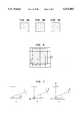
- FIG. 1shows a schematic diagram of a module that uses Solder Ball Connections
- FIG. 2shows a cross-section of a ball soldered to the pad of the module substrate
- FIG. 3is a schematic of the module soldered to a printed circuit card
- FIG. 4is a bloc diagram of the system used in the inspection method according to the present invention.
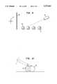
- FIGS. 5A-Cillustrate three examples of ball arrays which can be inspected with the inspection method, according to the present invention
- FIG. 6shows successive views of groups of balls that are recorded using the method that determines the centrality of the array of balls
- FIG. 7shows three representations showing the deviations to be taken into account when the height of the balls is determined
- FIG. 8shows a schematic diagram of the system used in determining the flatness of the array of balls used in the inspection method, according to the present invention
- FIG. 9is a photograph showing the view of the illuminated balls, according to the method of the present invention.
- FIG. 10illustrates the correction to be introduced in the determination of the height when the ball is not at its theoretical position
- FIG. 11illustrates a misalignment between the camera and the table carrying the module to be inspected
- FIG. 12shows a pair of juxtaposed views that includes drift between first and second views
- FIG. 13shows two Juxtaposed views separated by a gap caused by a scaling problem
- FIG. 14illustrates the deviation between the image plane and the vertical plane in determining the Z scale
- FIG. 15shows the light ring used as the light source of the inspection method, according to the present invention.
- the module to be inspectedis generally a Solder Ball Connection (SBC) module shown in FIG. 1.
- Solder balls 10replace the conventional pins used for the connections.
- Substrate 14contains a plurality of circuitry layers which connect chips 12 to the balls, which are used as input/output terminals. The chips are encapsulated by cap 16. As shown in FIG. 2, each ball 10 is connected to a pad 18 of substrate 14 by a point of solder 20.
- modulesare attached to a printed circuit board by soldering the balls on the receiving pads 22 of the board 24 as shown in FIG. 3. If the array of balls soldered on the module is not planar, some balls 10 may be too far removed from pad 22 to be soldered thereto, and no connection to the board is achieved. Furthermore, if the matrix of balls is not regular, some balls may not face their corresponding pad, and again no connection will ensue.
- the method of inspection according to the present inventionenables the array of balls to be inspected with high degree of accuracy and speed. Such a method achieves its best results when used with the inspection apparatus illustrated in FIG. 4.
- a module 30is placed on a motorized table or support which is movable along its X and Y axes.
- the motion of table 32is controlled by microprocessor 34 (e.g., an IBM PS/2) via control unit 36.
- microprocessor 34e.g., an IBM PS/2
- the tablecan be moved so that the X and Y coordinates of the modules can be adjusted with precision.
- Two cameras 38 and 40are used to perform an inspection of the positioning of the ball in the X,Y plane and height with respect to the horizontal plane. As will be described hereinafter, camera 38 is used to measure the centrality of the ball array, whereas camera 40 is used to sense the flatness of the array.
- the two cameras 38 and 40are coupled to a controller 42 which is connected to microprocessor 34. Controller 42 processes the vision algorithms, computes the results, adjusts the light intensity, and selects the camera.
- Microprocessor 34performs all controls, synchronizes the axes motion with the vision process and is used to interface with the operator.
- the first step of the inspectionconsists in checking the uniformity of the array of balls, i.e., measuring the centrality of the array.
- the principleis not to sense the position of each ball with respect to an absolute reference, such as the edge of the substrate, but to define the relative position of each ball in the array with respect to other balls forming the array.
- three modules A, B, and Care illustrated in FIG. 5.
- the first module Ahas an array forming an irregular matrix. Such a module will be discarded.
- module Bhas a shifted matrix of balls
- module Chas a tilted matrix of balls; these modules B and C can be kept since, in both instances, the matrix of balls is regularly shaped.
- the stepconsists in measuring accurately the position of each ball, computing a best fitting grid which is a theoretical grid matching at best all the balls, and computing the deviation between each ball against its theoretical position in the best fitting grid.
- a measureis achieved by means of the vertical camera 38 (see FIG. 4) which takes successive views of the array in the manner illustrated in FIG. 6, wherein the module 30 is shown in grey.
- Each view 1, 2, 3, . . . 6, 7corresponds to a matrix of m ⁇ n balls.
- one viewcan take the image of 20 balls corresponding to a 4 ⁇ 5 matrix.
- the parameters m and nare determined by the distance which the table carrying the module is moved to whenever a new view is required.
- the technique of taking views in this manneris sometimes called "Boustrophedon", and results in scanning the whole module in a minimum amount of time.
- the image magnification and the scaledepend on the distance object/camera. Thus, if the distance grows, the magnification becomes smaller.
- the specifications on the thickness of the moduleare large, e.g., 0.9 mm.
- the scalescan lead to erroneous results if the difference is as small as 0.1 mm.
- Thruput considerationspreclude calibrating the tool for each module. Therefore, the distance module/camera must be adapted to a predetermined scale which is applicable to each module.
- the apparatus performing the inspectionuses two cameras with different viewing angles resulting in the ability of processing stereo-vision to detect variations in height. Two views are processed from the same object and 3D information is computed. This information is compared with information stored during the calibration step described hereinafter.
- the Z axisis automatically adjusted to maintain the height between the camera and the module constant. Such a method enables determining a deviation of the order of 10 ⁇ m.
- the difference in height for each moduleis easily determined with the help of the two cameras.
- diagram Athere is no height difference; therefore no adjustment is necessary.
- diagram Bthe height difference Dh is determined by measuring the deviation D1 determined by the tilted camera. ##EQU1##
- the vertical camerais moved by the distance Dh before further processing.
- the height of the ballsis determined by taking a view for each group of four balls.
- a light source 50is located opposite camera 40.
- a diffuser 52is placed between the light source 50 and the balls 10. With such a light system, it is very easy for the camera to capture a view of the light reflection 54 at the top of the balls, as illustrated in FIG. 9 by the four crosses shown on top of the four balls.
- the tableis then moved to take a view of the next four balls.
- the technique of taking the views of the balls(Boustrophedon) is the same as it was for measuring the alignment of the balls.
- a plane fitting at most the top of the ballsis computed using the Least Square Regression technique. If X(i,j), Y(i,j), and Z(i,j) are the coordinates of each ball top, the equation of a plane including such a point is:
- the processconsists in computing three parameters of the plane which minimizes the sum of the squared distances, i.e., :
- Dis derived with respect to the three unknown coefficients a, b, c, and the derivatives equal to zero.
- Equations (4) and (5)become
- the deviations between the balls of the array and the best fitting planeare then computed.
- the best fitting planeis offset so that the new plane, i.e., the inspection plane, includes the top of the lowest ball in the array.
- the deviations between the balls and the inspection planeare computed.
- the computed deviationsare compared with the specifications. If they compare favorably, the module is accepted; otherwise, the module is discarded.
- the calibrationis particularly important. It consists in determining the ratio camera pixel/real size. This ratio is called “scale” and depends on the optical magnification.
- a CCD (coupled charge device) camerais used.
- a pixelis not square, so the scale for the two axes X and Y has to be determined.
- one axial motionbeing executed between two image acquisitions, one must also take into account the drift resulting from the misalignment between axes of the camera and the table, as shown in FIG. 11.
- Calibrationis achieved in two steps: a coarse calibration and a fine calibration.
- coarse calibrationone image is snapped (20 balls for centrality and 4 balls for flatness) to determine the approximate pixel scale.
- the average of the deviation between the ballsis computed by combining them two by two.
- the fine calibrationgives, with high accuracy, the scales X and Y. It also provides the drifts X and Y for centrality measurements. These are obtained using a vertical camera (Note: if the X and Y table axes are not perpendicular, drift X is different from drift Y). For flatness measurements, the camera is tilted at an angle of about 15° with respect to the horizontal plane.
- the calibrationprovides the Z scale and the reference for the Z axis, i.e., the distance between the module and the vertical camera used for the centrality.
- the complete moduleis preferably processed by the inspection method according to the invention using the scale resulting from the coarse calibration.
- Driftis illustrated in FIG. 12 showing two successive views.
- the slope of the moduleis computed by averaging all the balls of each view over all the views. Such a slope is called a "correction" (CORR).
- CORRcorrected
- VARIvariation from one view to the next
- the Z scaleFor measurement of the flatness, the Z scale needs to be determined.
- the angle ⁇ between the image plane and the vertical planemust be computed, as illustrated in FIG. 14. If RS is the real scale and SS the observed scale, the following equations can be set:
Landscapes
- Engineering & Computer Science (AREA)
- Physics & Mathematics (AREA)
- General Physics & Mathematics (AREA)
- Health & Medical Sciences (AREA)
- Immunology (AREA)
- Computer Hardware Design (AREA)
- General Health & Medical Sciences (AREA)
- Analytical Chemistry (AREA)
- Chemical & Material Sciences (AREA)
- Pathology (AREA)
- Life Sciences & Earth Sciences (AREA)
- Biochemistry (AREA)
- Microelectronics & Electronic Packaging (AREA)
- Computer Vision & Pattern Recognition (AREA)
- Electromagnetism (AREA)
- Toxicology (AREA)
- General Engineering & Computer Science (AREA)
- Length Measuring Devices By Optical Means (AREA)
Abstract
Description
The invention relates to a method of inspection used in the manufacture of integrated circuit modules, and more particularly to a method of inspecting an array of solder ball connections used for outside connections in an integrated circuit module in order to determine if the inspected module meets the manufacturing specifications.
In many integrated circuit modules and in particular in SBC (Solder Ball Connection) modules, solder balls replace conventional connection pins. The substrate generally includes a plurality of layers which interconnect the chips to solder balls used as input/outputs. Such modules are routinely soldered to a printed circuit board by means of a matrix of conductive pads.
The overall reliability of the bonds created by the soldered ball process is adversely affected by defective balls. By way of example, if a ball has an insufficient height, no electrical connection exists between the ball and its corresponding pad on the circuit board.
In the past, several types of bonding inspection apparatus have been proposed. For instance, U.S. Pat. No. 4,688,939 describes an inspection apparatus of solder bumps by placing a chip carrier on a platform beneath a light ring which is coupled to a television camera. Light directed at an angle towards the sides of the chip carrier is reflected upwardly into the camera by the solder bumps. The output signal of the camera, which varies with the intensity of the light reflected from the bumps, is processed by a visual system to obtain a one-dimensional plot of the light intensity. The one-dimensional plot is analyzed automatically by the system to detect missing or excessive solder bumps on the chip carrier.
In a second illustration, U.S. Pat. No. 5,058,178 relates to an apparatus wherein defective or missing solder bumps of a chip carrier are detected by first illuminating the carrier with dark field illumination. The image of the surface is captured by a television camera. The image is processed to detect defects by first creating a window within the image about each group of solder bumps and creating a bounding box for each bump in each window. Each set of attributes includes the number, size and location of both the windows and the boxes within each window; and similarly, the dimensions, shape and brightness of the image within each box. The value of each attribute is compared to a reference value that represents the attribute when no defects are present. If the attribute differs by more than a predetermined tolerance, it indicates the presence of a defect.
Present state of the art inspection apparatus check each solder bump and verify whether the bump meets the requirements that determine the presence or the absence of a defect. None of the present apparatus inspect the complete array of bumps (or balls) to determine whether they are correctly placed with respect to each other within the array.
Accordingly, it is an object of the invention to provide an automatic method of inspecting an array of balls used as connections in an integrated circuit module to determine whether the module meets its manufacturing specifications.
Another object of the invention is to provide an automatic method of inspecting the centrality and the flatness of an array of balls used as connections in an integrated circuit module.
Still another object of the invention is to provide an automatic method of inspecting an array of balls used as connections in an integrated circuit module by checking the alignment and the flatness of the balls without utilizing an absolute reference, such as the edge of the substrate.
Accordingly, the present invention relates to a method of inspecting an array of balls used as connections of integrated circuit modules, using an inspection apparatus having a microprocessor, a support for holding in place the module to be inspected, wherein positioning of the support is controlled by the microprocessor, at least one camera connected to the microprocessor, the camera providing images of the balls, the balls being illuminated by a light source. The method, according to the present invention, includes measuring the X and Y coordinates of each ball forming the array of balls to determine the best fitting grid of the balls, detecting the Z coordinate of each ball to determine a best fitting plane for the array of balls, offsetting the best fitting plane to ensure that the offset plane includes the lowest ball of the array, computing the deviation between each ball of the array and the offset plane, and comparing the computed deviation against a predetermined specification to determine whether the module is in compliance with the specification.
The objects, features and advantages of the subject invention will become more evident with the following description read in connection with the accompanying drawings wherein:
FIG. 1 shows a schematic diagram of a module that uses Solder Ball Connections;
FIG. 2 shows a cross-section of a ball soldered to the pad of the module substrate;
FIG. 3 is a schematic of the module soldered to a printed circuit card;
FIG. 4 is a bloc diagram of the system used in the inspection method according to the present invention;
FIGS. 5A-C illustrate three examples of ball arrays which can be inspected with the inspection method, according to the present invention;
FIG. 6 shows successive views of groups of balls that are recorded using the method that determines the centrality of the array of balls;
FIG. 7 shows three representations showing the deviations to be taken into account when the height of the balls is determined;
FIG. 8 shows a schematic diagram of the system used in determining the flatness of the array of balls used in the inspection method, according to the present invention;
FIG. 9 is a photograph showing the view of the illuminated balls, according to the method of the present invention;
FIG. 10 illustrates the correction to be introduced in the determination of the height when the ball is not at its theoretical position;
FIG. 11 illustrates a misalignment between the camera and the table carrying the module to be inspected;
FIG. 12 shows a pair of juxtaposed views that includes drift between first and second views;
FIG. 13 shows two Juxtaposed views separated by a gap caused by a scaling problem;
FIG. 14 illustrates the deviation between the image plane and the vertical plane in determining the Z scale; and
FIG. 15 shows the light ring used as the light source of the inspection method, according to the present invention.
The module to be inspected is generally a Solder Ball Connection (SBC) module shown in FIG. 1.Solder balls 10 replace the conventional pins used for the connections.Substrate 14 contains a plurality of circuitry layers which connectchips 12 to the balls, which are used as input/output terminals. The chips are encapsulated bycap 16. As shown in FIG. 2, eachball 10 is connected to apad 18 ofsubstrate 14 by a point ofsolder 20.
Several modules are attached to a printed circuit board by soldering the balls on thereceiving pads 22 of theboard 24 as shown in FIG. 3. If the array of balls soldered on the module is not planar, someballs 10 may be too far removed frompad 22 to be soldered thereto, and no connection to the board is achieved. Furthermore, if the matrix of balls is not regular, some balls may not face their corresponding pad, and again no connection will ensue.
The method of inspection according to the present invention enables the array of balls to be inspected with high degree of accuracy and speed. Such a method achieves its best results when used with the inspection apparatus illustrated in FIG. 4. Amodule 30 is placed on a motorized table or support which is movable along its X and Y axes. The motion of table 32 is controlled by microprocessor 34 (e.g., an IBM PS/2) viacontrol unit 36. The table can be moved so that the X and Y coordinates of the modules can be adjusted with precision.
Twocameras camera 38 is used to measure the centrality of the ball array, whereascamera 40 is used to sense the flatness of the array. The twocameras controller 42 which is connected tomicroprocessor 34.Controller 42 processes the vision algorithms, computes the results, adjusts the light intensity, and selects the camera.Microprocessor 34 performs all controls, synchronizes the axes motion with the vision process and is used to interface with the operator.
The first step of the inspection consists in checking the uniformity of the array of balls, i.e., measuring the centrality of the array. The principle is not to sense the position of each ball with respect to an absolute reference, such as the edge of the substrate, but to define the relative position of each ball in the array with respect to other balls forming the array. Thus, three modules A, B, and C are illustrated in FIG. 5. The first module A has an array forming an irregular matrix. Such a module will be discarded. Conversely, module B has a shifted matrix of balls, and module C has a tilted matrix of balls; these modules B and C can be kept since, in both instances, the matrix of balls is regularly shaped.
More particularly, the step consists in measuring accurately the position of each ball, computing a best fitting grid which is a theoretical grid matching at best all the balls, and computing the deviation between each ball against its theoretical position in the best fitting grid. Such a measure is achieved by means of the vertical camera 38 (see FIG. 4) which takes successive views of the array in the manner illustrated in FIG. 6, wherein themodule 30 is shown in grey. Eachview 1, 2, 3, . . . 6, 7 corresponds to a matrix of m×n balls. Thus, one view can take the image of 20 balls corresponding to a 4×5 matrix. The parameters m and n are determined by the distance which the table carrying the module is moved to whenever a new view is required. The technique of taking views in this manner is sometimes called "Boustrophedon", and results in scanning the whole module in a minimum amount of time.
The views are then combined to form a composite image of the module. This can, potentially, create difficulties due to the misalignment of the camera with respect to the table. Such a problem resulting from an image "drift" is solved by a calibration step which will be described hereinafter.
The image magnification and the scale depend on the distance object/camera. Thus, if the distance grows, the magnification becomes smaller. The specifications on the thickness of the module are large, e.g., 0.9 mm. The scales, however, can lead to erroneous results if the difference is as small as 0.1 mm. Thruput considerations preclude calibrating the tool for each module. Therefore, the distance module/camera must be adapted to a predetermined scale which is applicable to each module. The apparatus performing the inspection uses two cameras with different viewing angles resulting in the ability of processing stereo-vision to detect variations in height. Two views are processed from the same object and 3D information is computed. This information is compared with information stored during the calibration step described hereinafter. The Z axis is automatically adjusted to maintain the height between the camera and the module constant. Such a method enables determining a deviation of the order of 10 μm.
As illustrated in FIG. 7, the difference in height for each module is easily determined with the help of the two cameras. In diagram A, there is no height difference; therefore no adjustment is necessary. In diagram B, the height difference Dh is determined by measuring the deviation D1 determined by the tilted camera. ##EQU1##
In diagram C, in addition to the difference in height, there is also a difference D2 in the position detected by the vertical camera. In such a case, the height difference is: ##EQU2##
When the height difference has been accurately determined by measuring several balls and taking the average, the vertical camera is moved by the distance Dh before further processing.
The height of the balls is determined by taking a view for each group of four balls. As shown on FIG. 8, alight source 50 is located oppositecamera 40. In order to obtain a diffused light, adiffuser 52 is placed between thelight source 50 and theballs 10. With such a light system, it is very easy for the camera to capture a view of thelight reflection 54 at the top of the balls, as illustrated in FIG. 9 by the four crosses shown on top of the four balls.
For each ball, a correction of the height is necessary becauseball 10 is not at itstheoretical position 56, as shown in FIG. 10. Such a deviation with respect to the theoretical Y coordinate is known by measuring the alignment of the balls and determining the theoretical grid, as already described. The correction to be applied to the view is:
D=L. sin Φ,
wherein Y is the angle of the camera and L the deviation of the ball with respect to its theoretical position.
The table is then moved to take a view of the next four balls. The technique of taking the views of the balls (Boustrophedon) is the same as it was for measuring the alignment of the balls.
Once the height of the balls forming the array has been determined, corrected and stored, a plane fitting at most the top of the balls, called hereinafter the "best fitting plane", is computed using the Least Square Regression technique. If X(i,j), Y(i,j), and Z(i,j) are the coordinates of each ball top, the equation of a plane including such a point is:
Z.sub.plane =a.X(i,j)+b.Y(i,j)+c
The squared distance between any object and the plane is given by:
E(i,j)=[Z.sub.plane -Z(i,j)].sup.2
The process consists in computing three parameters of the plane which minimizes the sum of the squared distances, i.e., :
D=sum E(i,j),
wherein D is derived with respect to the three unknown coefficients a, b, c, and the derivatives equal to zero.
Let it be defined:
S=Z.sub.plane -Z(i,j)
S=a.X(i,j)+b.Y(i,j)+c-Z(i,j)
Therefore,
dE(i,j)/d* =2.dS/d*.S,
wherein * represents any one of a, b, c.
dE(i,j)/da=2.X(i,j).[a.X(i,j)+b.Y(i,j)+c-Z(i,j)]
dE(i,j)/db=2.Y(i,j).[a.X(i,j)+b.Y(i,j)+c-Z(i,j)]
dE(i,j)/dc=2.[a.X(i,j)+b.Y(i,j)+c-Z(i,j)]
These expressions are summed over the working set comprising n objects, and the results are equated to zero. ##EQU3##
This results in:
0=a.S4+b.S6+c.S1+S7 (1)
0=a.S6+b.S5+c.S2+S8 (2)
0=a.S1+b.S2+c.n+S3 (3)
Let
(1).S6-(2).S4 (4)
0=b.(S6.S6-S5.S4)+c.(S1.S6-S2.S4)+(S7.S6-S4.S8)
(2).S1-(3).S6 (5)
0=b.(S5.S1-S2.S6)+c.(S1.S2-n.S6)+(S8.S1-S3.S6)
Let it be further defined: ##EQU4##
Equations (4) and (5) become
0=b.A+c.B+C
0=b.D+c.E+F
Let
(4).E-(5).B
0=b.(A.E-D.B)+(C.E-F.B)
Then coefficient b is given by:
b=-(C.E-F.B)/(A.E-D.B)
It follows that:
a=-(b.S6+c.S1+S7)/S4, and
c=-(B.D-A.E)/(D.C-A.F)
The deviations between the balls of the array and the best fitting plane are then computed. The best fitting plane is offset so that the new plane, i.e., the inspection plane, includes the top of the lowest ball in the array. Again, the deviations between the balls and the inspection plane are computed. Finally, the computed deviations are compared with the specifications. If they compare favorably, the module is accepted; otherwise, the module is discarded.
Since the apparatus for performing the process according to the invention is an alignment tool, the calibration is particularly important. It consists in determining the ratio camera pixel/real size. This ratio is called "scale" and depends on the optical magnification.
Preferably, a CCD (coupled charge device) camera is used. In such a camera, a pixel is not square, so the scale for the two axes X and Y has to be determined. Furthermore, with one axial motion being executed between two image acquisitions, one must also take into account the drift resulting from the misalignment between axes of the camera and the table, as shown in FIG. 11.
Calibration is achieved in two steps: a coarse calibration and a fine calibration. During coarse calibration, one image is snapped (20 balls for centrality and 4 balls for flatness) to determine the approximate pixel scale. The average of the deviation between the balls is computed by combining them two by two.
The fine calibration gives, with high accuracy, the scales X and Y. It also provides the drifts X and Y for centrality measurements. These are obtained using a vertical camera (Note: if the X and Y table axes are not perpendicular, drift X is different from drift Y). For flatness measurements, the camera is tilted at an angle of about 15° with respect to the horizontal plane. The calibration provides the Z scale and the reference for the Z axis, i.e., the distance between the module and the vertical camera used for the centrality.
To perform a fine calibration, the complete module is preferably processed by the inspection method according to the invention using the scale resulting from the coarse calibration.
Drift is illustrated in FIG. 12 showing two successive views. The slope of the module is computed by averaging all the balls of each view over all the views. Such a slope is called a "correction" (CORR). The variation from one view to the next (VARI) is averaged over all the balls located at the image edges.
DRIFT=VARI (x,y)-CORR (x,y)
As far as the scale is concerned, such a problem is illustrated in FIG. 13 showing two views separated by a gap due to a scale problem. This problem is easily solved by noticing that R is not only the ratio of the value of the distance between the balls of the views but it is also the ratio of the "used scale" over the "real scale". Therefore, once R is computed, one may easily rectify the scale. It must be noted that the distances between balls are averaged over the complete module.
For measurement of the flatness, the Z scale needs to be determined. The angle θ between the image plane and the vertical plane must be computed, as illustrated in FIG. 14. If RS is the real scale and SS the observed scale, the following equations can be set:
RS(X)=SS(X)
RS(Y)=SS(X).R ##EQU5## With reference to FIG. 15 it must be noted that, in order to obtain an image that includes the balls without any shadow (which could disturb the measuring process), a non-directed and homogeneouslight source 60 called a "light ring" is used to illuminatemodule 30 during the inspection process. Such a light ring composed of LEDs 100 is highly advantageous in that it does not provide much heat which would constitute a nuisance for achieving inspection.
While the invention has been described with respect to a particular embodiment thereof, it will be apparent to those skilled in the art that variations may be made therein without departing from the spirit and the scope of the present invention.
Claims (17)
1. A method of inspecting balls within a ball grid array, the balls used as connections of integrated circuit modules, using an inspection apparatus having a microprocessor, a support for holding in place the modules to be inspected, wherein positioning of the support is controlled by the microprocessor, at least one camera connected to the microprocessor, the camera providing images of the balls, the balls being illuminated by a light source, said method comprising the steps of:
measuring a centrality of the grid array by taking views of successive adjoining sub-arrays of said grid array and combining said views to form a composite image of the module;
from said composite image, measuring the X and Y coordinates of each of the balls forming said grid array to determine a best fitting grid of said balls;
determining the Z coordinate measured from the top of each of said balls to define a best fitting plane applicable to said array, based on said best fitting grid;
offsetting said best fitting plane so that the plane includes the lowest ball of said array of balls;
computing a deviation in the Z direction between each of said balls of said array and said offset plane; and
comparing the computed deviation against a predetermined specification and discarding as defective any said modules exceeding said first deviation and said deviation in the Z direction.
2. The method as recited in claim 1, wherein the step of determining the best fitting grid of said balls further comprises the steps of:
measuring the position of each of the balls of said array for each of said modules;
determining from the position of each of the balls the best fitting grid to best match all the balls of said array of balls; and
computing the deviation in the x and y directions between each of said balls and its position within said best fitting grid.
3. The method as recited in claim 2, wherein said step of measuring the position of each of said balls in said array further comprises taking successive juxtaposed views with the camera of sections of said array of balls, each section comprising a sub-array of m by n of said balls.
4. The method as recited in claim 1, wherein the step of determining the Z coordinate of each of said balls of said array further comprises taking views with a tilted camera of successive juxtaposed rows of said array of balls, wherein said balls are illuminated by the light source placed opposite to said camera, and wherein the image of said balls taken by said camera corresponds to a light reflection at the top of said ball.
5. The method as recited in claim 1, wherein said step of determining the best fitting plane for said array of balls further comprises applying a Least Square Regression technique to the computation of parameters that define said plane so as to minimize the sum of squared distances between the plane and the balls.
6. The method as recited in claim 4, wherein the Z coordinate measured at the top of each of said balls and detected by the tilted camera is corrected by determining a deviation of the position of each of said balls with respect to a predetermined position in said best fitting grid.
7. The method as recited in claim 6, wherein prior to the step of detecting the Z coordinate of each of said balls, the relative position of the module with respect to the vertical camera is adjusted to account for the thickness of the module.
8. The method as recited in claim 1, further comprising a calibration step that includes a coarse and a fine calibration, said calibration being performed prior to inspecting the module, wherein a scale and a drift required by the inspection are defined.
9. The method as recited in claim 8, wherein said coarse calibration further comprises obtaining an image of said array of balls and computing an average of the deviation between said balls, wherein said balls are combined two by two to define a pixel scale.
10. The method as recited in claim 9, wherein said fine calibration further comprises:
determining the drift resulting from a misalignment between an axis of said camera and an axis of the support by computing the difference between the variation between two successive views of said balls taken by the camera and the slope of the module with respect to the support;
determining the X and Y scales by computing the ratio of the distance between said balls captured by said camera in one of said views to the distance between balls in two of said views, and
determining the Z scale by using the angle 0 between the vertical plane and the image plane when a view is taken with a tilted camera.
11. A method of inspecting balls within a ball grid array, the balls used as connections of integrated circuit modules, using an inspection apparatus having a microprocessor, a support movable in the X and Y directions controlled by said microprocessor, first and second cameras coupled to said microprocessor for providing images of the balls, said method comprising the steps of:
a) measuring a centrality of the grid array by taking views of successive adjoining sub-arrays of said grid array and combining said views to form a composite image of the module;
b) combining said views to form an image of said array of balls;
c) from said image, measuring the position of each said balls, computing a best fitting grid and a first deviation in the X and Y directions between each of said balls and said best fitting grid;
d) determining the height of said balls with said second camera tilted with respect with said module, taking views of successive rows, while said balls are illuminated by a source of light placed opposite to said wherein an image of said balls in each said views corresponds to light reflections at the top of said balls;
e) computing a best fitting plane formed by said tops of said balls;
f) offsetting said best fitting plane by an amount determined by the top of the lowest of said balls in said array of balls to form an offset plane;
g) computing a deviation in the Z direction between said best fitting plane and said offset plane; and
h) comparing said first deviation and said deviation in the Z direction with predetermined specifications, and discarding as defective any said modules exceeding said first deviation and said deviation in the Z direction.
12. The method as recited in step d) of claim 11, further comprising the step of correcting said height of said tops of said balls by adjusting said height in accordance with said first deviation.
13. The method as recited in step d) of claim 11, wherein said first camera is adjusted to account for the thickness of said module.
14. The method as recited in claim 11, wherein calibration is performed prior to said inspection to quantify a drift that occurs while taking said views.
15. The method as recited in claim 14, wherein said calibration includes a coarse and a fine calibration.
16. The method as recited in claim 15, wherein said coarse calibration includes creating an image of said array of balls and subsequently computing a deviation in the X and Y directions between two of said balls by combining said balls two by two to determine an approximate pixel scale.
17. The method as recited in claim 15, wherein said fine calibration further comprises the steps of:
determining said drift resulting from a misalignment between said first camera and said support by computing a difference between a variation from one of said views to the next of said views taken with said first camera and the tilt of said module with respect to said support;
determining X and Y scales by computing a ratio of the distance between balls of one of said views over the distance between balls of two of said views; and
determining a Z scale by using an angle formed by a vertical plane and an image plane determined when a view is taken with said second camera.
Applications Claiming Priority (2)
| Application Number | Priority Date | Filing Date | Title |
|---|---|---|---|
| EP93480113AEP0638801B1 (en) | 1993-08-12 | 1993-08-12 | Method of inspecting the array of balls of an integrated circuit module |
| EP93480113.5 | 1993-09-17 |
Publications (1)
| Publication Number | Publication Date |
|---|---|
| US5574801Atrue US5574801A (en) | 1996-11-12 |
Family
ID=8214843
Family Applications (1)
| Application Number | Title | Priority Date | Filing Date |
|---|---|---|---|
| US08/289,972Expired - Fee RelatedUS5574801A (en) | 1993-08-12 | 1994-08-12 | Method of inspecting an array of solder ball connections of an integrated circuit module |
Country Status (3)
| Country | Link |
|---|---|
| US (1) | US5574801A (en) |
| EP (1) | EP0638801B1 (en) |
| DE (1) | DE69322775T2 (en) |
Cited By (84)
| Publication number | Priority date | Publication date | Assignee | Title |
|---|---|---|---|---|
| US5695667A (en)* | 1995-02-07 | 1997-12-09 | Matsushita Electric Industrial Co., Ltd. | Method and apparatus for mounting soldering balls onto electrodes of a substrate or a comparable electronic component |
| US5828449A (en)* | 1997-02-26 | 1998-10-27 | Acuity Imaging, Llc | Ring illumination reflective elements on a generally planar surface |
| US5831247A (en)* | 1995-06-19 | 1998-11-03 | Matsushita Electric Industrial Co., Ltd. | Apparatus and method for producing an electronic component provided with bumps |
| US5872870A (en) | 1996-02-16 | 1999-02-16 | Cognex Corporation | Machine vision methods for identifying extrema of objects in rotated reference frames |
| US5909504A (en) | 1996-03-15 | 1999-06-01 | Cognex Corporation | Method of testing a machine vision inspection system |
| US5926557A (en)* | 1997-02-26 | 1999-07-20 | Acuity Imaging, Llc | Inspection method |
| US5943125A (en)* | 1997-02-26 | 1999-08-24 | Acuity Imaging, Llc | Ring illumination apparatus for illuminating reflective elements on a generally planar surface |
| US5953130A (en) | 1997-01-06 | 1999-09-14 | Cognex Corporation | Machine vision methods and apparatus for machine vision illumination of an object |
| US5956134A (en)* | 1997-07-11 | 1999-09-21 | Semiconductor Technologies & Instruments, Inc. | Inspection system and method for leads of semiconductor devices |
| US5960125A (en) | 1996-11-21 | 1999-09-28 | Cognex Corporation | Nonfeedback-based machine vision method for determining a calibration relationship between a camera and a moveable object |
| US5974169A (en) | 1997-03-20 | 1999-10-26 | Cognex Corporation | Machine vision methods for determining characteristics of an object using boundary points and bounding regions |
| US5978080A (en) | 1997-09-25 | 1999-11-02 | Cognex Corporation | Machine vision methods using feedback to determine an orientation, pixel width and pixel height of a field of view |
| US5978502A (en) | 1996-04-01 | 1999-11-02 | Cognex Corporation | Machine vision methods for determining characteristics of three-dimensional objects |
| US6026176A (en) | 1995-07-25 | 2000-02-15 | Cognex Corporation | Machine vision methods and articles of manufacture for ball grid array inspection |
| US6025854A (en) | 1997-12-31 | 2000-02-15 | Cognex Corporation | Method and apparatus for high speed image acquisition |
| WO2000010115A1 (en)* | 1998-08-14 | 2000-02-24 | Acuity Imaging, Llc | System and method for image subtraction for ball and bumped grid array inspection |
| US6055054A (en)* | 1997-05-05 | 2000-04-25 | Beaty; Elwin M. | Three dimensional inspection system |
| US6055328A (en)* | 1998-01-16 | 2000-04-25 | Cognex Corporation | Analyzing an acquired arrangement of object locations |
| US6056190A (en)* | 1997-02-06 | 2000-05-02 | Speedline Technologies, Inc. | Solder ball placement apparatus |
| US6064757A (en)* | 1998-01-16 | 2000-05-16 | Elwin M. Beaty | Process for three dimensional inspection of electronic components |
| US6067379A (en) | 1988-12-09 | 2000-05-23 | Cognex Corporation | Method and apparatus for locating patterns in an optical image |
| US6067376A (en)* | 1998-01-16 | 2000-05-23 | Cognex Corporation | Classifying pixels of an image |
| US6075881A (en) | 1997-03-18 | 2000-06-13 | Cognex Corporation | Machine vision methods for identifying collinear sets of points from an image |
| US6115491A (en)* | 1996-02-27 | 2000-09-05 | Cyberoptics Corporation | Apparatus and method for estimating background tilt and offset |
| US6118524A (en)* | 1997-02-26 | 2000-09-12 | Acuity Imaging, Llc | Arc illumination apparatus and method |
| US6119337A (en)* | 1998-03-10 | 2000-09-19 | Matsushita Electric Industrial Co., Ltd. | Method of mounting conductive balls |
| US6130959A (en)* | 1997-07-16 | 2000-10-10 | Cognex Corporation | Analyzing an image of an arrangement of discrete objects |
| US6137893A (en) | 1996-10-07 | 2000-10-24 | Cognex Corporation | Machine vision calibration targets and methods of determining their location and orientation in an image |
| US6141033A (en) | 1997-05-15 | 2000-10-31 | Cognex Corporation | Bandwidth reduction of multichannel images for machine vision |
| US6151406A (en)* | 1997-10-09 | 2000-11-21 | Cognex Corporation | Method and apparatus for locating ball grid array packages from two-dimensional image data |
| US6170737B1 (en) | 1997-02-06 | 2001-01-09 | Speedline Technologies, Inc. | Solder ball placement method |
| US6177682B1 (en)* | 1998-10-21 | 2001-01-23 | Novacam Tyechnologies Inc. | Inspection of ball grid arrays (BGA) by using shadow images of the solder balls |
| US6201892B1 (en) | 1997-02-26 | 2001-03-13 | Acuity Imaging, Llc | System and method for arithmetic operations for electronic package inspection |
| US6199741B1 (en) | 1998-12-09 | 2001-03-13 | International Business Machines Corporation | Enhanced pad design for substrate |
| US6202918B1 (en) | 1997-01-28 | 2001-03-20 | Eric Hertz | Method and apparatus for placing conductive preforms |
| US6215915B1 (en) | 1998-02-20 | 2001-04-10 | Cognex Corporation | Image processing methods and apparatus for separable, general affine transformation of an image |
| US6230963B1 (en) | 1997-01-28 | 2001-05-15 | Eric L. Hertz | Method and apparatus using colored foils for placing conductive preforms |
| US6236769B1 (en) | 1998-01-28 | 2001-05-22 | Cognex Corporation | Machine vision systems and methods for morphological transformation of an image with zero or other uniform offsets |
| US6259827B1 (en) | 1996-03-21 | 2001-07-10 | Cognex Corporation | Machine vision methods for enhancing the contrast between an object and its background using multiple on-axis images |
| US6268275B1 (en) | 1998-10-08 | 2001-07-31 | Micron Technology, Inc. | Method of locating conductive spheres utilizing screen and hopper of solder balls |
| US6282328B1 (en) | 1998-01-28 | 2001-08-28 | Cognex Corporation | Machine vision systems and methods for morphological transformation of an image with non-uniform offsets |
| US6289117B1 (en) | 1997-07-16 | 2001-09-11 | Cognex Corporation | Analysis of an image of a pattern of discrete objects |
| US6298149B1 (en) | 1996-03-21 | 2001-10-02 | Cognex Corporation | Semiconductor device image inspection with contrast enhancement |
| SG85125A1 (en)* | 1998-08-05 | 2001-12-19 | Nat Semiconductor Corp | Grid array inspection system and method |
| US20020015780A1 (en)* | 2000-07-11 | 2002-02-07 | William Holm | Method and apparatus for applying viscous medium onto a substrate |
| US20020014602A1 (en)* | 2000-07-11 | 2002-02-07 | William Holm | Method and apparatus for providing a substrate with viscous medium |
| US6360935B1 (en)* | 1999-01-26 | 2002-03-26 | Board Of Regents Of The University Of Texas System | Apparatus and method for assessing solderability |
| US6381366B1 (en) | 1998-12-18 | 2002-04-30 | Cognex Corporation | Machine vision methods and system for boundary point-based comparison of patterns and images |
| US6381375B1 (en) | 1998-02-20 | 2002-04-30 | Cognex Corporation | Methods and apparatus for generating a projection of an image |
| US6412685B2 (en) | 1997-01-28 | 2002-07-02 | Galahad, Co. | Method and apparatus for release and optional inspection for conductive preforms placement apparatus |
| US20020158643A1 (en)* | 2001-01-12 | 2002-10-31 | Electroglas Inc. | Method and apparatus for generating values for selected pixels used in evaluating semiconductor wafer bumps |
| US6522777B1 (en) | 1998-07-08 | 2003-02-18 | Ppt Vision, Inc. | Combined 3D- and 2D-scanning machine-vision system and method |
| US6533159B1 (en) | 1998-10-07 | 2003-03-18 | Micron Technology, Inc. | Apparatus for attaching solder balls to BGA package utilizing a tool to pick and dip the solder ball in flux |
| US6608647B1 (en) | 1997-06-24 | 2003-08-19 | Cognex Corporation | Methods and apparatus for charge coupled device image acquisition with independent integration and readout |
| US6641030B1 (en) | 1997-02-06 | 2003-11-04 | Speedline Technologies, Inc. | Method and apparatus for placing solder balls on a substrate |
| US6657656B1 (en)* | 1998-11-25 | 2003-12-02 | Shibuya Kogyo Co., Ltd. | Mount inspection apparatus |
| US6684402B1 (en) | 1999-12-01 | 2004-01-27 | Cognex Technology And Investment Corporation | Control methods and apparatus for coupling multiple image acquisition devices to a digital data processor |
| US6687402B1 (en) | 1998-12-18 | 2004-02-03 | Cognex Corporation | Machine vision methods and systems for boundary feature comparison of patterns and images |
| US6748104B1 (en) | 2000-03-24 | 2004-06-08 | Cognex Corporation | Methods and apparatus for machine vision inspection using single and multiple templates or patterns |
| US20040109602A1 (en)* | 2002-11-22 | 2004-06-10 | Yusuke Konno | Method and apparatus for inspecting a bump electrode |
| US20040148128A1 (en)* | 2003-01-23 | 2004-07-29 | Sun Microsystems, Inc. | Methods and apparatus for inspecting centerplane connectors |
| US6778282B1 (en)* | 1999-04-13 | 2004-08-17 | Icos Vision Systems N.V. | Measuring positions of coplanarity of contract elements of an electronic component with a flat illumination and two cameras |
| US6853751B1 (en)* | 2000-03-31 | 2005-02-08 | Cognex Technology And Investment Corporation | Location of generally rectangular shaped objects in an image |
| US20050094542A1 (en)* | 2003-10-29 | 2005-05-05 | Tdk Corporation | Inspection device and inspection method |
| US6915007B2 (en) | 1998-01-16 | 2005-07-05 | Elwin M. Beaty | Method and apparatus for three dimensional inspection of electronic components |
| US20050190961A1 (en)* | 1998-01-16 | 2005-09-01 | Beaty Elwin M. | Method of manufacturing electronic components including a method for three dimensional inspection |
| US6956963B2 (en) | 1998-07-08 | 2005-10-18 | Ismeca Europe Semiconductor Sa | Imaging for a machine-vision system |
| US20050249397A1 (en)* | 2002-11-28 | 2005-11-10 | Advantest Corporation | Position detecting apparatus, a position detecting method and an electronic component carrying apparatus |
| US7006669B1 (en) | 2000-12-31 | 2006-02-28 | Cognex Corporation | Machine vision method and apparatus for thresholding images of non-uniform materials |
| US7142301B2 (en) | 1999-07-08 | 2006-11-28 | Ppt Vision | Method and apparatus for adjusting illumination angle |
| US20070255455A1 (en)* | 2006-04-28 | 2007-11-01 | Symyx Technologies, Inc. | Robotic station for capturing both image and weight of a sample |
| US7353954B1 (en) | 1998-07-08 | 2008-04-08 | Charles A. Lemaire | Tray flipper and method for parts inspection |
| US7423743B2 (en) | 2000-12-29 | 2008-09-09 | Icos Vision Systems Nv | Method and an apparatus for measuring positions of contact elements of an electronic component |
| US20090074285A1 (en)* | 2006-05-15 | 2009-03-19 | Nikon Corporation | Surface inspection device |
| US7639861B2 (en) | 2005-09-14 | 2009-12-29 | Cognex Technology And Investment Corporation | Method and apparatus for backlighting a wafer during alignment |
| WO2009123808A3 (en)* | 2008-04-04 | 2010-01-14 | Research Triangle Institute | A solder bump bondig method, stencil. and system |
| US20100328435A1 (en)* | 2006-06-21 | 2010-12-30 | Yong Joo Puah | Method and apparatus for 3-dimensional vision and inspection of ball and like protrusions of electronic components |
| US8111904B2 (en) | 2005-10-07 | 2012-02-07 | Cognex Technology And Investment Corp. | Methods and apparatus for practical 3D vision system |
| US8162584B2 (en) | 2006-08-23 | 2012-04-24 | Cognex Corporation | Method and apparatus for semiconductor wafer alignment |
| US8368872B1 (en)* | 2011-07-15 | 2013-02-05 | Primax Electronics Ltd. | Method for determining planting ball number of camera module |
| US20130278750A1 (en)* | 2012-04-23 | 2013-10-24 | Metrospec Technology, L.L.C. | Self-learning machine vision system |
| US8643305B2 (en) | 1998-03-19 | 2014-02-04 | Lemaire Illumination Technologies, Llc | Apparatus for L.E.D. illumination |
| US9704232B2 (en) | 2014-03-18 | 2017-07-11 | Arizona Board of Regents of behalf of Arizona State University | Stereo vision measurement system and method |
| CN112834528A (en)* | 2021-01-06 | 2021-05-25 | 深圳格兰达智能装备股份有限公司 | 3D defect detection system and method |
Families Citing this family (21)
| Publication number | Priority date | Publication date | Assignee | Title |
|---|---|---|---|---|
| JP3551667B2 (en)* | 1996-12-04 | 2004-08-11 | 株式会社日立製作所 | Solder bump height measurement method |
| JP2000510248A (en)* | 1997-03-05 | 2000-08-08 | シーメンス アクチエンゲゼルシヤフト | Method for monitoring the presence of terminal balls |
| US6095661A (en) | 1998-03-19 | 2000-08-01 | Ppt Vision, Inc. | Method and apparatus for an L.E.D. flashlight |
| JP2000121338A (en)* | 1998-10-13 | 2000-04-28 | Yamagata Casio Co Ltd | Electronic component inspecting device |
| IES991081A2 (en)* | 1998-12-23 | 2000-07-26 | Mv Res Ltd | A measurement system |
| US6671397B1 (en) | 1998-12-23 | 2003-12-30 | M.V. Research Limited | Measurement system having a camera with a lens and a separate sensor |
| US6707545B1 (en) | 1999-09-07 | 2004-03-16 | Applied Materials, Inc. | Optical signal routing method and apparatus providing multiple inspection collection points on semiconductor manufacturing systems |
| US6630995B1 (en) | 1999-09-07 | 2003-10-07 | Applied Materials, Inc. | Method and apparatus for embedded substrate and system status monitoring |
| US6721045B1 (en) | 1999-09-07 | 2004-04-13 | Applied Materials, Inc. | Method and apparatus to provide embedded substrate process monitoring through consolidation of multiple process inspection techniques |
| US7012684B1 (en) | 1999-09-07 | 2006-03-14 | Applied Materials, Inc. | Method and apparatus to provide for automated process verification and hierarchical substrate examination |
| US6813032B1 (en) | 1999-09-07 | 2004-11-02 | Applied Materials, Inc. | Method and apparatus for enhanced embedded substrate inspection through process data collection and substrate imaging techniques |
| US6693708B1 (en) | 1999-09-07 | 2004-02-17 | Applied Materials, Inc. | Method and apparatus for substrate surface inspection using spectral profiling techniques |
| US6707544B1 (en) | 1999-09-07 | 2004-03-16 | Applied Materials, Inc. | Particle detection and embedded vision system to enhance substrate yield and throughput |
| US6525331B1 (en) | 1999-12-01 | 2003-02-25 | Nanyang Technological University | Ball grid array (BGA) package on-line non-contact inspection method and system |
| US6509559B1 (en) | 2000-06-20 | 2003-01-21 | Ppt Vision, Inc. | Binary optical grating and method for generating a moire pattern for 3D imaging |
| US6486963B1 (en) | 2000-06-20 | 2002-11-26 | Ppt Vision, Inc. | Precision 3D scanner base and method for measuring manufactured parts |
| US6501554B1 (en) | 2000-06-20 | 2002-12-31 | Ppt Vision, Inc. | 3D scanner and method for measuring heights and angles of manufactured parts |
| US20020196336A1 (en) | 2001-06-19 | 2002-12-26 | Applied Materials, Inc. | Method and apparatus for substrate imaging |
| AU2003253368A1 (en)* | 2002-07-25 | 2004-02-16 | Matsushita Electric Industrial Co., Ltd. | Apparatus and method for insepecting cream solder printed on a substrate |
| WO2004088399A1 (en)* | 2003-03-31 | 2004-10-14 | Hits Co., Ltd. | Lcd cell edge inspection apparatus and method thereof |
| WO2005024403A1 (en)* | 2003-09-05 | 2005-03-17 | Semiconductor Technologies & Instruments Pte Ltd. | Ball grid array inspection system and method |
Citations (14)
| Publication number | Priority date | Publication date | Assignee | Title |
|---|---|---|---|---|
| US3721825A (en)* | 1970-12-03 | 1973-03-20 | J Rasmussen | Method and apparatus for analysis of liquid residues using nuclear reactions |
| US4296474A (en)* | 1977-09-06 | 1981-10-20 | Deere & Company | Inspection system and apparatus therefor |
| US4677473A (en)* | 1985-06-21 | 1987-06-30 | Matsushita Electric Works, Ltd. | Soldering inspection system and method therefor |
| US4688939A (en)* | 1985-12-27 | 1987-08-25 | At&T Technologies, Inc. | Method and apparatus for inspecting articles |
| US5058178A (en)* | 1989-12-21 | 1991-10-15 | At&T Bell Laboratories | Method and apparatus for inspection of specular, three-dimensional features |
| EP0471196A2 (en)* | 1990-08-13 | 1992-02-19 | Siemens Aktiengesellschaft | Image analysis method |
| EP0472041A2 (en)* | 1990-08-24 | 1992-02-26 | Hitachi, Ltd. | Method and apparatus for detecting deformations of leads of semiconductor device |
| US5108024A (en)* | 1991-06-03 | 1992-04-28 | Motorola, Inc. | Method of inspecting solder joints |
| US5134665A (en)* | 1990-03-08 | 1992-07-28 | Mitsubishi Denki Kabushiki Kaisha | Apparatus and method of inspecting solder printing |
| US5137362A (en)* | 1990-03-26 | 1992-08-11 | Motorola, Inc. | Automatic package inspection method |
| US5161202A (en)* | 1990-07-18 | 1992-11-03 | Dainippon Screen Mfg. Co. Ltd. | Method of and device for inspecting pattern of printed circuit board |
| US5368217A (en)* | 1993-08-25 | 1994-11-29 | Microelectronics And Computer Technology Corporation | High force compression flip chip bonding method and system |
| US5376790A (en)* | 1992-03-13 | 1994-12-27 | Park Scientific Instruments | Scanning probe microscope |
| US5394246A (en)* | 1991-12-02 | 1995-02-28 | Kabushiki Kaisha Shinkawa | Bonding wire inspection apparatus and method |
- 1993
- 1993-08-12EPEP93480113Apatent/EP0638801B1/ennot_activeExpired - Lifetime
- 1993-08-12DEDE69322775Tpatent/DE69322775T2/ennot_activeExpired - Fee Related
- 1994
- 1994-08-12USUS08/289,972patent/US5574801A/ennot_activeExpired - Fee Related
Patent Citations (14)
| Publication number | Priority date | Publication date | Assignee | Title |
|---|---|---|---|---|
| US3721825A (en)* | 1970-12-03 | 1973-03-20 | J Rasmussen | Method and apparatus for analysis of liquid residues using nuclear reactions |
| US4296474A (en)* | 1977-09-06 | 1981-10-20 | Deere & Company | Inspection system and apparatus therefor |
| US4677473A (en)* | 1985-06-21 | 1987-06-30 | Matsushita Electric Works, Ltd. | Soldering inspection system and method therefor |
| US4688939A (en)* | 1985-12-27 | 1987-08-25 | At&T Technologies, Inc. | Method and apparatus for inspecting articles |
| US5058178A (en)* | 1989-12-21 | 1991-10-15 | At&T Bell Laboratories | Method and apparatus for inspection of specular, three-dimensional features |
| US5134665A (en)* | 1990-03-08 | 1992-07-28 | Mitsubishi Denki Kabushiki Kaisha | Apparatus and method of inspecting solder printing |
| US5137362A (en)* | 1990-03-26 | 1992-08-11 | Motorola, Inc. | Automatic package inspection method |
| US5161202A (en)* | 1990-07-18 | 1992-11-03 | Dainippon Screen Mfg. Co. Ltd. | Method of and device for inspecting pattern of printed circuit board |
| EP0471196A2 (en)* | 1990-08-13 | 1992-02-19 | Siemens Aktiengesellschaft | Image analysis method |
| EP0472041A2 (en)* | 1990-08-24 | 1992-02-26 | Hitachi, Ltd. | Method and apparatus for detecting deformations of leads of semiconductor device |
| US5108024A (en)* | 1991-06-03 | 1992-04-28 | Motorola, Inc. | Method of inspecting solder joints |
| US5394246A (en)* | 1991-12-02 | 1995-02-28 | Kabushiki Kaisha Shinkawa | Bonding wire inspection apparatus and method |
| US5376790A (en)* | 1992-03-13 | 1994-12-27 | Park Scientific Instruments | Scanning probe microscope |
| US5368217A (en)* | 1993-08-25 | 1994-11-29 | Microelectronics And Computer Technology Corporation | High force compression flip chip bonding method and system |
Non-Patent Citations (4)
| Title |
|---|
| Disclosed Anonymously No. 33317, "Solder Ball Connection (SBC) Co-Planarity with X-Ray Technology" Havant GB, Jan. 1992. |
| Disclosed Anonymously No. 33317, Solder Ball Connection (SBC) Co Planarity with X Ray Technology Havant GB, Jan. 1992.* |
| W. E. Blanz, et al., "Image Analysis Methods for Solder Ball Inspection in Integrated Circuit Manufacturing" IEEE, pp. 509-514, 1987. |
| W. E. Blanz, et al., Image Analysis Methods for Solder Ball Inspection in Integrated Circuit Manufacturing IEEE, pp. 509 514, 1987.* |
Cited By (143)
| Publication number | Priority date | Publication date | Assignee | Title |
|---|---|---|---|---|
| US6067379A (en) | 1988-12-09 | 2000-05-23 | Cognex Corporation | Method and apparatus for locating patterns in an optical image |
| US6013899A (en)* | 1995-02-07 | 2000-01-11 | Matsushita Electric Industrial Co., Ltd. | Method and apparatus for mounting soldering balls onto electrodes of a substrate or a comparable electronic component |
| US5695667A (en)* | 1995-02-07 | 1997-12-09 | Matsushita Electric Industrial Co., Ltd. | Method and apparatus for mounting soldering balls onto electrodes of a substrate or a comparable electronic component |
| US5831247A (en)* | 1995-06-19 | 1998-11-03 | Matsushita Electric Industrial Co., Ltd. | Apparatus and method for producing an electronic component provided with bumps |
| US6026176A (en) | 1995-07-25 | 2000-02-15 | Cognex Corporation | Machine vision methods and articles of manufacture for ball grid array inspection |
| US5872870A (en) | 1996-02-16 | 1999-02-16 | Cognex Corporation | Machine vision methods for identifying extrema of objects in rotated reference frames |
| US6385335B1 (en) | 1996-02-27 | 2002-05-07 | Cyberoptics Corp. | Apparatus and method for estimating background tilt and offset |
| US6115491A (en)* | 1996-02-27 | 2000-09-05 | Cyberoptics Corporation | Apparatus and method for estimating background tilt and offset |
| US5909504A (en) | 1996-03-15 | 1999-06-01 | Cognex Corporation | Method of testing a machine vision inspection system |
| US6298149B1 (en) | 1996-03-21 | 2001-10-02 | Cognex Corporation | Semiconductor device image inspection with contrast enhancement |
| US6396949B1 (en) | 1996-03-21 | 2002-05-28 | Cognex Corporation | Machine vision methods for image segmentation using multiple images |
| US6587582B1 (en) | 1996-03-21 | 2003-07-01 | Cognex Corporation | Semiconductor device image inspection with contrast enhancement |
| US6259827B1 (en) | 1996-03-21 | 2001-07-10 | Cognex Corporation | Machine vision methods for enhancing the contrast between an object and its background using multiple on-axis images |
| US5978502A (en) | 1996-04-01 | 1999-11-02 | Cognex Corporation | Machine vision methods for determining characteristics of three-dimensional objects |
| US6137893A (en) | 1996-10-07 | 2000-10-24 | Cognex Corporation | Machine vision calibration targets and methods of determining their location and orientation in an image |
| US6301396B1 (en) | 1996-11-21 | 2001-10-09 | Cognex Corporation | Nonfeedback-based machine vision methods for determining a calibration relationship between a camera and a moveable object |
| US5960125A (en) | 1996-11-21 | 1999-09-28 | Cognex Corporation | Nonfeedback-based machine vision method for determining a calibration relationship between a camera and a moveable object |
| US5953130A (en) | 1997-01-06 | 1999-09-14 | Cognex Corporation | Machine vision methods and apparatus for machine vision illumination of an object |
| US6230963B1 (en) | 1997-01-28 | 2001-05-15 | Eric L. Hertz | Method and apparatus using colored foils for placing conductive preforms |
| US6202918B1 (en) | 1997-01-28 | 2001-03-20 | Eric Hertz | Method and apparatus for placing conductive preforms |
| US6412685B2 (en) | 1997-01-28 | 2002-07-02 | Galahad, Co. | Method and apparatus for release and optional inspection for conductive preforms placement apparatus |
| US6056190A (en)* | 1997-02-06 | 2000-05-02 | Speedline Technologies, Inc. | Solder ball placement apparatus |
| US6427903B1 (en) | 1997-02-06 | 2002-08-06 | Speedline Technologies, Inc. | Solder ball placement apparatus |
| US6170737B1 (en) | 1997-02-06 | 2001-01-09 | Speedline Technologies, Inc. | Solder ball placement method |
| US6641030B1 (en) | 1997-02-06 | 2003-11-04 | Speedline Technologies, Inc. | Method and apparatus for placing solder balls on a substrate |
| US5926557A (en)* | 1997-02-26 | 1999-07-20 | Acuity Imaging, Llc | Inspection method |
| US6236747B1 (en) | 1997-02-26 | 2001-05-22 | Acuity Imaging, Llc | System and method for image subtraction for ball and bumped grid array inspection |
| US6118524A (en)* | 1997-02-26 | 2000-09-12 | Acuity Imaging, Llc | Arc illumination apparatus and method |
| US5828449A (en)* | 1997-02-26 | 1998-10-27 | Acuity Imaging, Llc | Ring illumination reflective elements on a generally planar surface |
| US5943125A (en)* | 1997-02-26 | 1999-08-24 | Acuity Imaging, Llc | Ring illumination apparatus for illuminating reflective elements on a generally planar surface |
| US6201892B1 (en) | 1997-02-26 | 2001-03-13 | Acuity Imaging, Llc | System and method for arithmetic operations for electronic package inspection |
| US6075881A (en) | 1997-03-18 | 2000-06-13 | Cognex Corporation | Machine vision methods for identifying collinear sets of points from an image |
| US5974169A (en) | 1997-03-20 | 1999-10-26 | Cognex Corporation | Machine vision methods for determining characteristics of an object using boundary points and bounding regions |
| US6055054A (en)* | 1997-05-05 | 2000-04-25 | Beaty; Elwin M. | Three dimensional inspection system |
| US6141033A (en) | 1997-05-15 | 2000-10-31 | Cognex Corporation | Bandwidth reduction of multichannel images for machine vision |
| US6608647B1 (en) | 1997-06-24 | 2003-08-19 | Cognex Corporation | Methods and apparatus for charge coupled device image acquisition with independent integration and readout |
| US5956134A (en)* | 1997-07-11 | 1999-09-21 | Semiconductor Technologies & Instruments, Inc. | Inspection system and method for leads of semiconductor devices |
| US6289117B1 (en) | 1997-07-16 | 2001-09-11 | Cognex Corporation | Analysis of an image of a pattern of discrete objects |
| US6130959A (en)* | 1997-07-16 | 2000-10-10 | Cognex Corporation | Analyzing an image of an arrangement of discrete objects |
| US5978080A (en) | 1997-09-25 | 1999-11-02 | Cognex Corporation | Machine vision methods using feedback to determine an orientation, pixel width and pixel height of a field of view |
| US6151406A (en)* | 1997-10-09 | 2000-11-21 | Cognex Corporation | Method and apparatus for locating ball grid array packages from two-dimensional image data |
| US6396942B1 (en) | 1997-10-09 | 2002-05-28 | Cognex Corporation | Method and apparatus for locating ball grid array packages from two-dimensional image data |
| US6025854A (en) | 1997-12-31 | 2000-02-15 | Cognex Corporation | Method and apparatus for high speed image acquisition |
| US6067376A (en)* | 1998-01-16 | 2000-05-23 | Cognex Corporation | Classifying pixels of an image |
| US6064756A (en)* | 1998-01-16 | 2000-05-16 | Elwin M. Beaty | Apparatus for three dimensional inspection of electronic components |
| US7508974B2 (en) | 1998-01-16 | 2009-03-24 | Scanner Technologies Corporation | Electronic component products and method of manufacturing electronic component products |
| US6055328A (en)* | 1998-01-16 | 2000-04-25 | Cognex Corporation | Analyzing an acquired arrangement of object locations |
| US7085411B2 (en) | 1998-01-16 | 2006-08-01 | Scanner Technologies Corporation | Method of manufacturing electronic components including a method for three dimensional inspection |
| US6862365B1 (en)* | 1998-01-16 | 2005-03-01 | Elwin Beaty & Elaine Beaty | Method and apparatus for three dimensional inspection of electronic components |
| US6064757A (en)* | 1998-01-16 | 2000-05-16 | Elwin M. Beaty | Process for three dimensional inspection of electronic components |
| US7079678B2 (en) | 1998-01-16 | 2006-07-18 | Scanner Technologies Corporation | Electronic component products made according to a process that includes a method for three dimensional inspection |
| US6915007B2 (en) | 1998-01-16 | 2005-07-05 | Elwin M. Beaty | Method and apparatus for three dimensional inspection of electronic components |
| US6353676B1 (en) | 1998-01-16 | 2002-03-05 | Cognex Coporation | Analyzing an acquired arrangement of object locations |
| US20050190961A1 (en)* | 1998-01-16 | 2005-09-01 | Beaty Elwin M. | Method of manufacturing electronic components including a method for three dimensional inspection |
| US20050190960A1 (en)* | 1998-01-16 | 2005-09-01 | Beaty Elwin M. | Electronic component products made according to a process that includes a method for three dimensional inspection |
| US20050189657A1 (en)* | 1998-01-16 | 2005-09-01 | Beaty Elwin M. | Electronic component products and method of manufacturing electronic component products |
| US6072898A (en)* | 1998-01-16 | 2000-06-06 | Beaty; Elwin M. | Method and apparatus for three dimensional inspection of electronic components |
| US6282328B1 (en) | 1998-01-28 | 2001-08-28 | Cognex Corporation | Machine vision systems and methods for morphological transformation of an image with non-uniform offsets |
| US6236769B1 (en) | 1998-01-28 | 2001-05-22 | Cognex Corporation | Machine vision systems and methods for morphological transformation of an image with zero or other uniform offsets |
| US6381375B1 (en) | 1998-02-20 | 2002-04-30 | Cognex Corporation | Methods and apparatus for generating a projection of an image |
| US6215915B1 (en) | 1998-02-20 | 2001-04-10 | Cognex Corporation | Image processing methods and apparatus for separable, general affine transformation of an image |
| US6119337A (en)* | 1998-03-10 | 2000-09-19 | Matsushita Electric Industrial Co., Ltd. | Method of mounting conductive balls |
| US8643305B2 (en) | 1998-03-19 | 2014-02-04 | Lemaire Illumination Technologies, Llc | Apparatus for L.E.D. illumination |
| US9907137B1 (en) | 1998-03-19 | 2018-02-27 | Lemaire Illumination Technologies, Llc | Pulsed L.E.D. illumination |
| US8829808B1 (en) | 1998-03-19 | 2014-09-09 | Led Tech Development, Llc | Apparatus and method for pulsed L.E.D. illumination |
| US7719670B2 (en) | 1998-07-08 | 2010-05-18 | Charles A. Lemaire | Parts manipulation, inspection, and replacement system and method |
| US8408379B2 (en) | 1998-07-08 | 2013-04-02 | Charles A. Lemaire | Parts manipulation, inspection, and replacement |
| US8286780B2 (en) | 1998-07-08 | 2012-10-16 | Charles A. Lemaire | Parts manipulation, inspection, and replacement system and method |
| US8056700B2 (en) | 1998-07-08 | 2011-11-15 | Charles A. Lemaire | Tray flipper, tray, and method for parts inspection |
| US6522777B1 (en) | 1998-07-08 | 2003-02-18 | Ppt Vision, Inc. | Combined 3D- and 2D-scanning machine-vision system and method |
| US7773209B2 (en) | 1998-07-08 | 2010-08-10 | Charles A. Lemaire | Method and apparatus for parts manipulation, inspection, and replacement |
| US6956963B2 (en) | 1998-07-08 | 2005-10-18 | Ismeca Europe Semiconductor Sa | Imaging for a machine-vision system |
| US7353954B1 (en) | 1998-07-08 | 2008-04-08 | Charles A. Lemaire | Tray flipper and method for parts inspection |
| US20090180679A1 (en)* | 1998-07-08 | 2009-07-16 | Charles A. Lemaire | Method and apparatus for parts manipulation, inspection, and replacement |
| US20090078620A1 (en)* | 1998-07-08 | 2009-03-26 | Charles A. Lemaire | Tray flipper, tray, and method for parts inspection |
| US20090073427A1 (en)* | 1998-07-08 | 2009-03-19 | Charles A. Lemaire | Parts manipulation, inspection, and replacement system and method |
| SG85125A1 (en)* | 1998-08-05 | 2001-12-19 | Nat Semiconductor Corp | Grid array inspection system and method |
| WO2000010115A1 (en)* | 1998-08-14 | 2000-02-24 | Acuity Imaging, Llc | System and method for image subtraction for ball and bumped grid array inspection |
| US20030111508A1 (en)* | 1998-10-07 | 2003-06-19 | Cobbley Chad A. | Apparatus for attaching solder balls to BGA package utilizing a tool to pick and dip the solder ball in flux |
| US7644853B2 (en) | 1998-10-07 | 2010-01-12 | Micron Technology, Inc. | Apparatus for attaching solder balls to BGA package utilizing a tool to pick and dip the solder ball in flux |
| US20060027624A1 (en)* | 1998-10-07 | 2006-02-09 | Cobbley Chad A | Apparatus for attaching solder balls to BGA package utilizing a tool to pick and dip the solder ball in flux |
| US6957760B2 (en) | 1998-10-07 | 2005-10-25 | Micron Technology, Inc. | Apparatus for attaching solder balls to BGA package utilizing a tool to pick and dip the solder ball in flux |
| US6844216B2 (en) | 1998-10-07 | 2005-01-18 | Micron Technology, Inc. | Method of attaching solder balls to BGA package utilizing a tool to pick and dip the solder ball in flux |
| US6595408B1 (en) | 1998-10-07 | 2003-07-22 | Micron Technology, Inc. | Method of attaching solder balls to BGA package utilizing a tool to pick and dip the solder ball in flux prior to placement |
| US20030121957A1 (en)* | 1998-10-07 | 2003-07-03 | Cobbley Chad A. | Method of attaching solder balls to BGA package utilizing a tool to pick and dip the solder ball in flux |
| US6533159B1 (en) | 1998-10-07 | 2003-03-18 | Micron Technology, Inc. | Apparatus for attaching solder balls to BGA package utilizing a tool to pick and dip the solder ball in flux |
| US20050056681A1 (en)* | 1998-10-08 | 2005-03-17 | Cobbley Chad A. | Method of locating conductive spheres utilizing screen and hopper of solder balls |
| US20030110626A1 (en)* | 1998-10-08 | 2003-06-19 | Cobbley Chad A. | Method of locating conductive spheres utilizing screen and hopper of solder balls |
| US6551917B2 (en) | 1998-10-08 | 2003-04-22 | Micron Technology, Inc. | Method of locating conductive spheres utilizing screen and hopper of solder balls |
| US20050056682A1 (en)* | 1998-10-08 | 2005-03-17 | Cobbley Chad A. | Method of locating conductive spheres utilizing screen and hopper of solder balls |
| US7635079B1 (en) | 1998-10-08 | 2009-12-22 | Micron Technology, Inc. | System for locating conductive sphere utilizing screen and hopper of solder balls |
| US7105432B2 (en) | 1998-10-08 | 2006-09-12 | Micron Technology, Inc. | Method of locating conductive spheres utilizing screen and hopper of solder balls |
| US7275676B2 (en) | 1998-10-08 | 2007-10-02 | Micron Technology, Inc. | Apparatus for locating conductive spheres utilizing screen and hopper of solder balls |
| US6268275B1 (en) | 1998-10-08 | 2001-07-31 | Micron Technology, Inc. | Method of locating conductive spheres utilizing screen and hopper of solder balls |
| US6177682B1 (en)* | 1998-10-21 | 2001-01-23 | Novacam Tyechnologies Inc. | Inspection of ball grid arrays (BGA) by using shadow images of the solder balls |
| US6657656B1 (en)* | 1998-11-25 | 2003-12-02 | Shibuya Kogyo Co., Ltd. | Mount inspection apparatus |
| US6940168B2 (en) | 1998-12-09 | 2005-09-06 | International Business Machines Corporation | Enhanced pad design for substrate |
| US20010010321A1 (en)* | 1998-12-09 | 2001-08-02 | Garrity John Joseph | Enhanced pad design for substrate |
| US6720665B2 (en) | 1998-12-09 | 2004-04-13 | International Business Machines Corporation | Enhanced pad design for substrate |
| US6199741B1 (en) | 1998-12-09 | 2001-03-13 | International Business Machines Corporation | Enhanced pad design for substrate |
| US6687402B1 (en) | 1998-12-18 | 2004-02-03 | Cognex Corporation | Machine vision methods and systems for boundary feature comparison of patterns and images |
| US6381366B1 (en) | 1998-12-18 | 2002-04-30 | Cognex Corporation | Machine vision methods and system for boundary point-based comparison of patterns and images |
| US6360935B1 (en)* | 1999-01-26 | 2002-03-26 | Board Of Regents Of The University Of Texas System | Apparatus and method for assessing solderability |
| US6778282B1 (en)* | 1999-04-13 | 2004-08-17 | Icos Vision Systems N.V. | Measuring positions of coplanarity of contract elements of an electronic component with a flat illumination and two cameras |
| US7142301B2 (en) | 1999-07-08 | 2006-11-28 | Ppt Vision | Method and apparatus for adjusting illumination angle |
| US7557920B2 (en) | 1999-07-08 | 2009-07-07 | Lebens Gary A | Method and apparatus for auto-adjusting illumination |
| US6684402B1 (en) | 1999-12-01 | 2004-01-27 | Cognex Technology And Investment Corporation | Control methods and apparatus for coupling multiple image acquisition devices to a digital data processor |
| US6748104B1 (en) | 2000-03-24 | 2004-06-08 | Cognex Corporation | Methods and apparatus for machine vision inspection using single and multiple templates or patterns |
| US6853751B1 (en)* | 2000-03-31 | 2005-02-08 | Cognex Technology And Investment Corporation | Location of generally rectangular shaped objects in an image |
| US7201802B2 (en)* | 2000-07-11 | 2007-04-10 | Mydata Automation Ab | Apparatus for providing a substrate with viscous medium |
| US20020015780A1 (en)* | 2000-07-11 | 2002-02-07 | William Holm | Method and apparatus for applying viscous medium onto a substrate |
| US7931933B2 (en) | 2000-07-11 | 2011-04-26 | Mydata Automation Ab | Method and apparatus for providing a substrate with viscous medium |
| US20070137558A1 (en)* | 2000-07-11 | 2007-06-21 | William Holm | Method and apparatus for applying viscous medium onto a substrate |
| US20060275538A1 (en)* | 2000-07-11 | 2006-12-07 | William Holm | Method and apparatus for providing a substrate with viscous medium |
| US20020014602A1 (en)* | 2000-07-11 | 2002-02-07 | William Holm | Method and apparatus for providing a substrate with viscous medium |
| US7600548B2 (en) | 2000-07-11 | 2009-10-13 | Mydata Automation Ab | Method and apparatus for applying viscous medium onto a substrate |
| US7757391B2 (en) | 2000-07-11 | 2010-07-20 | Mydata Automation Ab | Method for applying viscous medium on a substrate |
| US7423743B2 (en) | 2000-12-29 | 2008-09-09 | Icos Vision Systems Nv | Method and an apparatus for measuring positions of contact elements of an electronic component |
| US7006669B1 (en) | 2000-12-31 | 2006-02-28 | Cognex Corporation | Machine vision method and apparatus for thresholding images of non-uniform materials |
| US20030025517A1 (en)* | 2001-01-12 | 2003-02-06 | Electrogas, Inc. | Method and apparatus for determining the location of an alignment mark on a wafer |
| US6547409B2 (en) | 2001-01-12 | 2003-04-15 | Electroglas, Inc. | Method and apparatus for illuminating projecting features on the surface of a semiconductor wafer |
| US20020158643A1 (en)* | 2001-01-12 | 2002-10-31 | Electroglas Inc. | Method and apparatus for generating values for selected pixels used in evaluating semiconductor wafer bumps |
| US20040109602A1 (en)* | 2002-11-22 | 2004-06-10 | Yusuke Konno | Method and apparatus for inspecting a bump electrode |
| US20050249397A1 (en)* | 2002-11-28 | 2005-11-10 | Advantest Corporation | Position detecting apparatus, a position detecting method and an electronic component carrying apparatus |
| US7471819B2 (en)* | 2002-11-28 | 2008-12-30 | Advantest Corporation | Position detecting apparatus, a position detecting method and an electronic component carrying apparatus |
| US7742071B2 (en) | 2003-01-23 | 2010-06-22 | Oracle America, Inc. | Methods and apparatus for inspecting centerplane connectors |
| US20040148128A1 (en)* | 2003-01-23 | 2004-07-29 | Sun Microsystems, Inc. | Methods and apparatus for inspecting centerplane connectors |
| US20050094542A1 (en)* | 2003-10-29 | 2005-05-05 | Tdk Corporation | Inspection device and inspection method |
| US7576769B2 (en)* | 2003-10-29 | 2009-08-18 | Tdk Corporation | Inspection device and inspection method |
| US7639861B2 (en) | 2005-09-14 | 2009-12-29 | Cognex Technology And Investment Corporation | Method and apparatus for backlighting a wafer during alignment |
| US8111904B2 (en) | 2005-10-07 | 2012-02-07 | Cognex Technology And Investment Corp. | Methods and apparatus for practical 3D vision system |
| US7848848B2 (en)* | 2006-04-28 | 2010-12-07 | Freeslate, Inc. | Robotic station for capturing both image and weight of a sample |
| US20070255455A1 (en)* | 2006-04-28 | 2007-11-01 | Symyx Technologies, Inc. | Robotic station for capturing both image and weight of a sample |
| US20090074285A1 (en)* | 2006-05-15 | 2009-03-19 | Nikon Corporation | Surface inspection device |
| US8885040B2 (en)* | 2006-06-21 | 2014-11-11 | Generic Power Pte Ltd. | Method and apparatus for 3-dimensional vision and inspection of ball and like protrusions of electronic components |
| US20100328435A1 (en)* | 2006-06-21 | 2010-12-30 | Yong Joo Puah | Method and apparatus for 3-dimensional vision and inspection of ball and like protrusions of electronic components |
| US8162584B2 (en) | 2006-08-23 | 2012-04-24 | Cognex Corporation | Method and apparatus for semiconductor wafer alignment |
| WO2009123808A3 (en)* | 2008-04-04 | 2010-01-14 | Research Triangle Institute | A solder bump bondig method, stencil. and system |
| US8368872B1 (en)* | 2011-07-15 | 2013-02-05 | Primax Electronics Ltd. | Method for determining planting ball number of camera module |
| TWI500317B (en)* | 2011-07-15 | 2015-09-11 | Primax Electronics Ltd | Method for determining amount of planting ball of camera module |
| US20130278750A1 (en)* | 2012-04-23 | 2013-10-24 | Metrospec Technology, L.L.C. | Self-learning machine vision system |
| US9704232B2 (en) | 2014-03-18 | 2017-07-11 | Arizona Board of Regents of behalf of Arizona State University | Stereo vision measurement system and method |
| CN112834528A (en)* | 2021-01-06 | 2021-05-25 | 深圳格兰达智能装备股份有限公司 | 3D defect detection system and method |
Also Published As
| Publication number | Publication date |
|---|---|
| EP0638801B1 (en) | 1998-12-23 |
| DE69322775T2 (en) | 1999-07-22 |
| EP0638801A1 (en) | 1995-02-15 |
| DE69322775D1 (en) | 1999-02-04 |
Similar Documents
| Publication | Publication Date | Title |
|---|---|---|
| US5574801A (en) | Method of inspecting an array of solder ball connections of an integrated circuit module | |
| US7034272B1 (en) | Method and apparatus for evaluating integrated circuit packages having three dimensional features | |
| US6055055A (en) | Cross optical axis inspection system for integrated circuits | |
| US5563703A (en) | Lead coplanarity inspection apparatus and method thereof | |
| US4959898A (en) | Surface mount machine with lead coplanarity verifier | |
| US5815275A (en) | Method and system for triangulation-based, 3-D imaging utilizing an angled scanning beam of radiant energy | |
| US6879403B2 (en) | Three dimensional scanning camera | |
| EP2387796B1 (en) | System and method for inspecting a wafer | |
| US6064757A (en) | Process for three dimensional inspection of electronic components | |
| US5621530A (en) | Apparatus and method for verifying the coplanarity of a ball grid array | |
| US8885040B2 (en) | Method and apparatus for 3-dimensional vision and inspection of ball and like protrusions of electronic components | |
| JP3005294B2 (en) | Grid array inspection system and method | |
| US6141040A (en) | Measurement and inspection of leads on integrated circuit packages | |
| US20090123060A1 (en) | inspection system | |
| WO2010082900A2 (en) | System and method for inspecting a wafer | |
| KR20010040998A (en) | Automatic inspection system with stereovision | |
| US6242756B1 (en) | Cross optical axis inspection system for integrated circuits | |
| WO2002029357A2 (en) | Method and apparatus for evaluating integrated circuit packages having three dimensional features | |
| US5838434A (en) | Semiconductor device lead calibration unit | |
| JPH0864999A (en) | Inspecting apparatus, measuring method for three-dimensional shape, and manufacture of product | |
| CN109219730B (en) | System and method for pin angle inspection using multi-view stereo vision | |
| US5489843A (en) | Apparatus and method for testing the calibration of electronic package lead inspection system | |
| JP2006317408A (en) | Warpage checker | |
| JPH11132735A (en) | Ic lead floating inspection device and inspection method | |
| KR100472966B1 (en) | Flatness level inspection apparatus and method of the ball grid array package |
Legal Events
| Date | Code | Title | Description |
|---|---|---|---|
| AS | Assignment | Owner name:INTERNATIONAL BUSINESS MACHINES CORPORATION, NEW Y Free format text:ASSIGNMENT OF ASSIGNORS INTEREST;ASSIGNOR:COLLET-BEILLON, OLIVIER;REEL/FRAME:007126/0035 Effective date:19940721 | |
| CC | Certificate of correction | ||
| FPAY | Fee payment | Year of fee payment:4 | |
| REMI | Maintenance fee reminder mailed | ||
| LAPS | Lapse for failure to pay maintenance fees | ||
| STCH | Information on status: patent discontinuation | Free format text:PATENT EXPIRED DUE TO NONPAYMENT OF MAINTENANCE FEES UNDER 37 CFR 1.362 | |
| FP | Lapsed due to failure to pay maintenance fee | Effective date:20041112 |