US5574738A - Multi-gigahertz frequency-modulated vertical-cavity surface emitting laser - Google Patents
Multi-gigahertz frequency-modulated vertical-cavity surface emitting laserDownload PDFInfo
- Publication number
- US5574738A US5574738AUS08/476,965US47696595AUS5574738AUS 5574738 AUS5574738 AUS 5574738AUS 47696595 AUS47696595 AUS 47696595AUS 5574738 AUS5574738 AUS 5574738A
- Authority
- US
- United States
- Prior art keywords
- vcsel
- frequency
- self
- terminal
- vcsels
- Prior art date
- Legal status (The legal status is an assumption and is not a legal conclusion. Google has not performed a legal analysis and makes no representation as to the accuracy of the status listed.)
- Expired - Lifetime
Links
- 239000006096absorbing agentSubstances0.000claimsabstractdescription42
- 238000004891communicationMethods0.000claimsabstractdescription6
- 230000000694effectsEffects0.000claimsdescription10
- 238000010521absorption reactionMethods0.000abstractdescription16
- 238000013461designMethods0.000abstractdescription10
- 238000002347injectionMethods0.000abstractdescription9
- 239000007924injectionSubstances0.000abstractdescription9
- 238000000034methodMethods0.000abstractdescription9
- 238000003491arrayMethods0.000abstractdescription7
- 238000004519manufacturing processMethods0.000abstractdescription7
- 230000004044responseEffects0.000abstractdescription3
- 230000008569processEffects0.000abstractdescription2
- 230000003287optical effectEffects0.000description15
- 230000010349pulsationEffects0.000description14
- 239000004065semiconductorSubstances0.000description13
- FTWRSWRBSVXQPI-UHFFFAOYSA-Nalumanylidynearsane;gallanylidynearsaneChemical compound[As]#[Al].[As]#[Ga]FTWRSWRBSVXQPI-UHFFFAOYSA-N0.000description12
- 239000000758substrateSubstances0.000description11
- JBRZTFJDHDCESZ-UHFFFAOYSA-NAsGaChemical compound[As]#[Ga]JBRZTFJDHDCESZ-UHFFFAOYSA-N0.000description10
- 239000000463materialSubstances0.000description10
- 229910001218Gallium arsenideInorganic materials0.000description9
- 230000010355oscillationEffects0.000description7
- 125000006850spacer groupChemical group0.000description7
- 239000011248coating agentSubstances0.000description5
- 238000000576coating methodMethods0.000description5
- 230000004888barrier functionEffects0.000description4
- 230000008859changeEffects0.000description4
- MDPILPRLPQYEEN-UHFFFAOYSA-Naluminium arsenideChemical compound[As]#[Al]MDPILPRLPQYEEN-UHFFFAOYSA-N0.000description3
- 230000008901benefitEffects0.000description3
- 238000009826distributionMethods0.000description3
- 238000005516engineering processMethods0.000description3
- 239000012535impuritySubstances0.000description3
- 238000002955isolationMethods0.000description3
- 238000000059patterningMethods0.000description3
- 238000002310reflectometryMethods0.000description3
- 238000013459approachMethods0.000description2
- 230000001427coherent effectEffects0.000description2
- 230000001419dependent effectEffects0.000description2
- 238000010586diagramMethods0.000description2
- 230000005684electric fieldEffects0.000description2
- 239000000835fiberSubstances0.000description2
- 239000007943implantSubstances0.000description2
- 230000010354integrationEffects0.000description2
- 238000005468ion implantationMethods0.000description2
- 229910052751metalInorganic materials0.000description2
- 239000002184metalSubstances0.000description2
- 238000001451molecular beam epitaxyMethods0.000description2
- 239000012071phaseSubstances0.000description2
- 230000010287polarizationEffects0.000description2
- 230000005701quantum confined stark effectEffects0.000description2
- 230000005855radiationEffects0.000description2
- 238000012935AveragingMethods0.000description1
- 230000004075alterationEffects0.000description1
- 238000004458analytical methodMethods0.000description1
- 239000013590bulk materialSubstances0.000description1
- 239000000969carrierSubstances0.000description1
- 239000002800charge carrierSubstances0.000description1
- 238000005229chemical vapour depositionMethods0.000description1
- 238000005253claddingMethods0.000description1
- 238000010276constructionMethods0.000description1
- 230000008878couplingEffects0.000description1
- 238000010168coupling processMethods0.000description1
- 238000005859coupling reactionMethods0.000description1
- 230000007423decreaseEffects0.000description1
- 230000003247decreasing effectEffects0.000description1
- 230000001934delayEffects0.000description1
- 238000001514detection methodMethods0.000description1
- 238000001914filtrationMethods0.000description1
- 238000003384imaging methodMethods0.000description1
- 238000010348incorporationMethods0.000description1
- 238000001465metallisationMethods0.000description1
- 238000002161passivationMethods0.000description1
- 230000000737periodic effectEffects0.000description1
- 238000012545processingMethods0.000description1
- 230000006798recombinationEffects0.000description1
- 238000005215recombinationMethods0.000description1
- 230000002269spontaneous effectEffects0.000description1
- 238000000927vapour-phase epitaxyMethods0.000description1
Images


Classifications
- H—ELECTRICITY
- H01—ELECTRIC ELEMENTS
- H01S—DEVICES USING THE PROCESS OF LIGHT AMPLIFICATION BY STIMULATED EMISSION OF RADIATION [LASER] TO AMPLIFY OR GENERATE LIGHT; DEVICES USING STIMULATED EMISSION OF ELECTROMAGNETIC RADIATION IN WAVE RANGES OTHER THAN OPTICAL
- H01S5/00—Semiconductor lasers
- H01S5/10—Construction or shape of the optical resonator, e.g. extended or external cavity, coupled cavities, bent-guide, varying width, thickness or composition of the active region
- H01S5/18—Surface-emitting [SE] lasers, e.g. having both horizontal and vertical cavities
- H01S5/183—Surface-emitting [SE] lasers, e.g. having both horizontal and vertical cavities having only vertical cavities, e.g. vertical cavity surface-emitting lasers [VCSEL]
- H—ELECTRICITY
- H01—ELECTRIC ELEMENTS
- H01S—DEVICES USING THE PROCESS OF LIGHT AMPLIFICATION BY STIMULATED EMISSION OF RADIATION [LASER] TO AMPLIFY OR GENERATE LIGHT; DEVICES USING STIMULATED EMISSION OF ELECTROMAGNETIC RADIATION IN WAVE RANGES OTHER THAN OPTICAL
- H01S5/00—Semiconductor lasers
- H01S5/06—Arrangements for controlling the laser output parameters, e.g. by operating on the active medium
- H01S5/062—Arrangements for controlling the laser output parameters, e.g. by operating on the active medium by varying the potential of the electrodes
- H01S5/06209—Arrangements for controlling the laser output parameters, e.g. by operating on the active medium by varying the potential of the electrodes in single-section lasers
- H01S5/06216—Pulse modulation or generation
- H—ELECTRICITY
- H01—ELECTRIC ELEMENTS
- H01S—DEVICES USING THE PROCESS OF LIGHT AMPLIFICATION BY STIMULATED EMISSION OF RADIATION [LASER] TO AMPLIFY OR GENERATE LIGHT; DEVICES USING STIMULATED EMISSION OF ELECTROMAGNETIC RADIATION IN WAVE RANGES OTHER THAN OPTICAL
- H01S5/00—Semiconductor lasers
- H01S5/06—Arrangements for controlling the laser output parameters, e.g. by operating on the active medium
- H01S5/0601—Arrangements for controlling the laser output parameters, e.g. by operating on the active medium comprising an absorbing region
- H—ELECTRICITY
- H01—ELECTRIC ELEMENTS
- H01S—DEVICES USING THE PROCESS OF LIGHT AMPLIFICATION BY STIMULATED EMISSION OF RADIATION [LASER] TO AMPLIFY OR GENERATE LIGHT; DEVICES USING STIMULATED EMISSION OF ELECTROMAGNETIC RADIATION IN WAVE RANGES OTHER THAN OPTICAL
- H01S5/00—Semiconductor lasers
- H01S5/06—Arrangements for controlling the laser output parameters, e.g. by operating on the active medium
- H01S5/0607—Arrangements for controlling the laser output parameters, e.g. by operating on the active medium by varying physical parameters other than the potential of the electrodes, e.g. by an electric or magnetic field, mechanical deformation, pressure, light, temperature
- H01S5/0614—Arrangements for controlling the laser output parameters, e.g. by operating on the active medium by varying physical parameters other than the potential of the electrodes, e.g. by an electric or magnetic field, mechanical deformation, pressure, light, temperature controlled by electric field, i.e. whereby an additional electric field is used to tune the bandgap, e.g. using the Stark-effect
- H—ELECTRICITY
- H01—ELECTRIC ELEMENTS
- H01S—DEVICES USING THE PROCESS OF LIGHT AMPLIFICATION BY STIMULATED EMISSION OF RADIATION [LASER] TO AMPLIFY OR GENERATE LIGHT; DEVICES USING STIMULATED EMISSION OF ELECTROMAGNETIC RADIATION IN WAVE RANGES OTHER THAN OPTICAL
- H01S5/00—Semiconductor lasers
- H01S5/06—Arrangements for controlling the laser output parameters, e.g. by operating on the active medium
- H01S5/065—Mode locking; Mode suppression; Mode selection ; Self pulsating
- H01S5/0658—Self-pulsating
- H—ELECTRICITY
- H01—ELECTRIC ELEMENTS
- H01S—DEVICES USING THE PROCESS OF LIGHT AMPLIFICATION BY STIMULATED EMISSION OF RADIATION [LASER] TO AMPLIFY OR GENERATE LIGHT; DEVICES USING STIMULATED EMISSION OF ELECTROMAGNETIC RADIATION IN WAVE RANGES OTHER THAN OPTICAL
- H01S5/00—Semiconductor lasers
- H01S5/40—Arrangement of two or more semiconductor lasers, not provided for in groups H01S5/02 - H01S5/30
- H01S5/42—Arrays of surface emitting lasers
- H01S5/423—Arrays of surface emitting lasers having a vertical cavity
Definitions
- This inventionrelates to the field of semiconductor lasers, and particularly relates to vertical cavity surface emitting lasers. More particularly, the invention relates to self-pulsing vertical cavity surface emitting lasers (VCSELs).
- VCSELsvertical cavity surface emitting lasers
- the typical semiconductor laseris a double heterostructure with a narrow bandgap, high refractive index layer surrounded on opposed major surfaces by wide bandgap, low refractive index layers.
- the low bandgap layeris termed the "active layer", and the bandgap and refractive index differences serve to confine both charge carriers and optical energy to the active layer or region.
- Opposite ends of the active layerhave mirror facets which form the laser cavity.
- the cladding layershave opposite conductivity types and when current is passed through the structure, electrons and holes combine in the active layer to generate light.
- VCSELvertical cavity surface emitting laser
- the laser describedhas an active region with bulk or one or more quantum well layers.
- the quantum well layersare interleaved with barrier layers.
- mirror stackswhich are formed by interleaved semiconductor layers having properties, such that each layer is typically a quarter wavelength thick at the wavelength (in the medium) of interest thereby forming the mirrors for the laser cavity.
- surface emitting devicescan be fabricated in arrays with relative ease while edge emitting devices can not be as easily fabricated.
- An array of laserscan be fabricated by growing the desired layers on a substrate and then patterning the layers to form the array. Individual lasers may be separately connected with appropriate contacts. Such arrays are potentially useful in such diverse applications as, for example, image processing inter-chip communications, i.e., optical interconnects, and so forth.
- typical edge-emitter lasersare turned on and off by varying the current flow through the device. This requires a relatively large change in the current through the device which is undesirable; the surface emitting laser, described below, requires lower drive current, and thus the change of current to switch the VCSEL need not be large.
- the present inventionis a controllable frequency-modulated, producible, vertical cavity surface emitting laser (VCSEL) and array.
- the inventionuses a saturable absorber (SA) contained within the VCSEL's distributed Bragg reflector (DBR), or spacer (as described in "Self-pulsations in vertical-cavity surface-emitting lasers," by D. Nugent et al., Electronics Letters, 31, pp. 43-44, Jan. 5, 1995).
- the saturable absorberstrategically placed, forces the VCSEL to self-pulsate (in the GHz-regime) at rates related to the local intensity, absorption, lifetime, and carrier density at the saturable absorber.
- This characteristicis exploited as a technique to frequency modulate a VCSEL.
- These operating conditionscan be controlled in real time by adjusting the injection current into the VCSEL itself, or by using a third terminal to modify the carrier density within the saturable absorber with additional current injection for a fixed VCSEL bias, or by reverse-biasing the saturable absorber thereby simultaneously altering the absorber's absorption and carrier lifetime and hence carrier density.
- the center frequency of oscillationcan be determined by the material, location and thickness of the saturable absorber, the mirror design, cavity Q and structure, and the laser size (and hence threshold current).
- VCSELs of this typecan have a particular modulation frequency range determined during fabrication and be further tuned during operation. The total operating range across the array can be increased by varying each element structure, and subsequently tuning it.
- VCSELs, arranged in an array, having differing sizes of apertures or other characteristicsmay be adjusted so as to form a phased array, with certain VCSELs turned on and others turned off, or a variation of frequency to achieve a certain direction of radiation by the resultant phased array, or a phased-antenna array controller.
- VCSELspermit the construction of highly effective, long range phased arrays functioning at high frequencies using low power with low cost, unsophisticated electronics, in contrast to radio frequency (RF) or millimeter (MM) based phased arrays.
- RFradio frequency
- MMmillimeter
- An additional advantagemay be determined by self-pulsation of the VCSEL which effectively decoheres the laser light output, wherein each individual pulse is reasonably coherent but the pulses together make the output laser light beam appear incoherent by averaging over the many pulses during the detection integration period, even though the laser beam itself may be in a coherent single transverse and longitudinal mode.
- Such decoherencecan be used to reduce modal noise in a multi-moded fiber medium to overcome mode selective noise penalties.
- a two terminal version of the VCSELis suited for decoherence purposes as a fixed VCSEL bias would be used for a predetermined frequency of self pulsation. A predetermined injected current would result in VCSEL emitting light pulsating at a certain frequency.
- the output of a VCSELmay be coupled into and conveyed by either a single mode or multi-mode medium or into a "free-space" lensed system.
- a controlled frequency modulated VCSELmay also serve as a low cost, low power optical local oscillator within numerous radio-frequency (RF) systems.
- FIG. 1is an illustration of a planar, current-guided, GaAs/AlGaAs top surface emitting vertical cavity laser.
- FIG. 2is a schematic of a VCSEL with an absorber.
- FIG. 3is a graph of pulsation frequency versus drive current for various positions of a saturable absorber in a VCSEL.
- FIG. 4is a cross-section of a three terminal frequency modulated VCSEL.
- FIG. 5are graphs for various voltage-current levels or light power and self-pulsation frequency versus drive current for a three terminal VCSEL.
- FIG. 6is a plot of the absorption coefficient of a quantum well region versus the applied (reverse) voltage.
- FIGS. 7a and 7bshow waveforms of VCSEL self-pulsation and modulation.
- FIG. 8ais an optical field distribution of a VCSEL.
- FIG. 8bshows light intensity versus position near the active region of a VCSEL.
- FIG. 9is a graph of typical light power-current-voltage (L-I-V) characteristics of a state-of-the-art GaAs/AlGaAs VCSEL.
- FIG. 10shows a hybrid-DBR spatial-filtered VCSEL having a dielectric mirror, with spatial filtering for single TEM 00 -mode control for improved performance and potential fabrication advantages.
- FIG. 11is a diagram of a modulator and the three terminal VCSEL for providing frequency-modulated self-pulsations.
- FIG. 12reveals an array of VCSELs having various sized and/or structured VCSEL apertures.
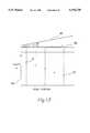
- FIG. 13is a cross section of an array of VCSELs having a Q-graded coating.
- FIG. 1is a diagram of a two terminal VCSEL 10. Formed on an n+ gallium arsenide (GaAs) substrate 14 is an n-contact 12. As indicated, substrate 14 is doped with impurities of a first type (i.e., n type). An n- mirror stack 16 is formed on substrate 14. Formed on stack 16 is a spacer 18. Spacer 18 has a bottom confinement layer 20 formed on stack 16, an active region 22 formed on layer 20 and a top confinement layer 24 formed on active region 22. A p- mirror stack 26 is formed on top confinement layer 24. A p- metal layer 28 is formed on stack 26. The emission region may have a passivation layer 30. Isolation region 29 restricts the area of the current flow 27 through the active region. Region 29 can be formed by deep H+ ion implantation or by other known techniques.
- Isolation region 29restricts the area of the current flow 27 through the active region. Region 29 can be formed by deep H+ ion implantation or by other known techniques.
- Spacer 18may contain quantum wells disposed between mirror stacks 16 and 26.
- Stacks 16 and 26are distributed Bragg reflector stacks.
- Quantum well active region 22has alternating layers of aluminum gallium arsenide (AlGaAs) barrier layers and GaAs well layers.
- Stacks 16 and 26have periodic layers of doped AlGaAs and aluminum arsenide (AlAs).
- the AlGaAs of stack 16is doped with the same type of impurity as substrate 14 (i.e., n type), and the AlGaAs of stack 26 is doped with the other kind of impurity (i.e., p type).
- Contact layers 12 and 28are ohmic contacts that allow appropriate electrical biasing of laser diode 10.
- active region 22emits light 32 which passes through stack 26.
- a saturable absorbersuch as layer 25, composed of GaAs, for example, to absorb light at wavelengths ( ⁇ ) less than 870 nm or composed of In x Ga 1-x As quantum wells (such as 80 angstroms in thickness and wherein x may be 0.2 as an example) to absorb light at wavelengths less than one micron.
- Layer 25can be of a ⁇ /4 order in thickness but need not be such.
- Layer 25can be situated anywhere in the stack of device 10. Instead, for instance, layer 31 may be the saturable absorber. Placement of the saturable absorber at a position in the cavity within layers 16 through 26 is influenced by the confinement factor. The saturable absorber may also be placed within spacer regions 20 or 24.
- saturable absorber layer 25is indicated to be a kth distance 90 of k one-quarter wavelengths from active region 22, as illustrated in FIG. 2 which is a schematic of a portion of VCSEL 10.
- Active region 22is illustrated with a thickness 94 and absorber 25 with a thickness 96.
- the thicknessshould be chosen in conjunction with the rest of the structure to maintain an adequate optically thick cavity.
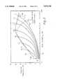
- FIG. 3shows the results of pulsation frequency versus drive current for various (k) SA positions of ⁇ /4 thickness for a VCSEL of a particular design but not necessarily VCSEL 10 of FIG. 1. Ibid., D. Nugent et al. The drive current for VCSEL 10 would be applied via contacts 28 and 12. These figures are noted again below. Note that pulsation frequency may be tuned by injection current and influenced by design (i.e., absorber position).
- a three terminal version of a vertical cavity surface emitting laseris shown in a sectional view in FIG. 4, in contrast to the two terminal VCSEL of FIG. 1.
- the frequency of the self pulsations of VCSEL 60 light 70may be modulated or tuned with a drive power of varying amplitude between terminals 52 and 50.
- the saturable absorbermay be situated anywhere between terminals 50 and 52.
- This inexpensive, low power device 60has a very large frequency modulation bandwidth.
- the application of current across terminals 48 and 50 of VCSEL 60can be constant, but tuned to give the right center self-pulsation frequency and/or light output. This configuration would result in minimal amplitude modulation of the VCSEL 60 light 70, as opposed to a two-terminal current-injected frequency-modulated VCSEL.
- the three terminal device 60has a fixed constant current between terminals 48 and 50 resulting in a particular voltage-current (VI) (reverse or forward biased) being applied between those terminals.
- VIvoltage-current
- FIG. 5three levels 74, 76 and 78 of VI 50-52 (voltage-current) across terminals (50 and 52) are illustrated with light power and the self-pulsation frequency f sp versus the drive current through terminals 48 and 50.
- the drive poweris used to modulate f sp .
- VI 78is greater than VI 76 which is greater than VI 74. As one can note, under these conditions for a given f sp , the drive current is less for a greater VI, as indicated by the dashed lines.
- FIG. 4Shown are substrate 34, regions 36 and 46 having a first conductivity type, active region 38, regions 40 and 42 having a second conductivity type, with saturable absorption region 44 having either or neither conductivity type depending on design and operating conditions.
- Region 44may comprise any number of bulk materials or one or more quantum wells, being normally absorbing at the lasing wavelength.
- Regions 36, 40, 42 and 46comprise mirrors which are depicted as interference mirrors. Region 36 comprises a first mirror. Only several layers are shown for reasons of clarity.
- Regions 40, 42, 44 and 46form a second distributed mirror with a cavity Q and hence an oscillation frequency controllable via power applied to the saturable absorber through contacts 50 and 52.
- the active regiontypically comprises one or more quantum well regions which are interleaved with barrier layers, i.e., layers having a bandgap greater than the bandgap of the quantum well region.
- barrier layersi.e., layers having a bandgap greater than the bandgap of the quantum well region.
- Contact 48may be physically made to substrate 34 if the substrate is conducting and not semi-insulating.
- Isolation region 54restricts the area of the current flow through the active region to the area generally under region 46.
- Isolation region 54can be formed by, e.g., deep ion implantation. Other forms of current and optical confinement may be utilized.
- the first and second interference mirrorsfurther comprise a plurality of interleaved first and second semiconductor layers with each layer having characteristics such that it is typically a quarter wavelength thick at the medium wavelength of interest thereby forming the respective interference mirror.
- the individual layers of the active region and the interference mirrorsare not described with particularity as those skilled in the art know the structure of these elements.
- substrate 34is conducting or semi-insulating GaAs
- regions 36, 40, 42 and 46comprise alternating layers of AlAs and AlGaAs, as an example, with properties as described in the previous paragraph.
- the active regionmay comprise one or multiple GaAs (or, e.g., In x Ga 1-x As) quantum wells interleaved with AlGaAs barrier layers.
- Saturable absorption (SA) region 44is optically coupled to region 40, i.e., the absorption due to the SA is within the distributed mirror incorporating regions 40, 42, 44 and 46.
- Region 46comprises interference mirror layers of, e.g., AlAs and AlGaAs, and has a first conductivity type.
- Those skilled in the artwill readily select appropriate layer thicknesses and these parameters need not be described in detail.
- the use of other semiconductorsis contemplated and appropriate choices will readily be made by those skilled in the art. For instance, other Group III-IV semiconductors may be used.
- the frequency of oscillation of the self-pulsing light emitted from the devicecan be varied by controlling the properties of the SA region within the VCSEL structure.
- An embodimentmay use current or voltage alteration of bulk or quantum-well material such as the quantum-confined Stark effect in quantum wells. This effect is well known and understood by those skilled in the art; the effect is described in Chapter 4 entitled “Nonlinear optical properties of semiconductor quantum wells," by D. S. Chemla et al., in Optical Nonlinearities and Instabilities in Semiconductors, pp. 339-347, (Academic Press 1988). Basically, the exciton absorption depends on the magnitude of the electric field in the quantum well. FIG.
- the absorption coefficient ⁇ of the quantum well regionvertically versus the applied voltage V horizontally for a wavelength longer than that of the zero field exciton.
- the absorption coefficient ⁇is plotted vertically versus the voltage V horizontally for an exemplary quantum-confined Stark effect region useful in the present device.
- a voltageis between contacts 52 and 50, i.e., a reverse bias p-i-n junction, and an increasing voltage corresponds to an increasing electric field and vice versa, Arbitrary units are used for purposes of exposition, The initial voltage is V b .
- the absorption coefficient ⁇can be varied a significant amount with a relatively small change in the applied voltage.
- the field-dependent Franz-Keldysh effectcan be used for an SA composed of bulk material, The use of this characteristic is noted below, Moreover, SA 44 of FIG. 4 may be forward biased to inject current into it also allowing frequency tuning.
- a vertical cavity surface emitting laserneeds relatively large reflectivities in both mirror stacks for lasing; typically, mirror stack reflectivities should be 99 percent or greater.
- the SA regionfunctions as a bias-dependent absorber, by appropriately varying the bias, the laser pulsation can be frequency modulated at different rates.
- a small voltage or current changemay be used to vary the absorption or carrier density of the SA and hence the frequency of the VCSEL self-pulsation.
- the magnitude of the current supplied through contacts 48 and 50 of device 60 of FIG. 4may remain essentially constant as the laser is modulated.
- the optical spatial field distribution of the surface emitting laser and the position of the saturable absorberare both engineering parameters. More or less absorption can be obtained by placing the absorber near a node or antinode, respectively. More or less absorption can also be obtained by increasing or decreasing the reflectivity of regions 40 and 36 of device 60, thereby coupling relatively less or more of the SA into the distributed mirror. Additionally, the material, thickness and/or design and number of the quantum wells, or of bulk materials, in SA 44 can be varied from that described herein. Those skilled in the art will readily select appropriate parameters.
- the inventionutilizes the saturable absorber in the optical cavity to achieve high-speed bias-controlled tuning of the self oscillation or pulsation frequency of a VCSEL or VCSEL array while maintaining constant current and hence minimizing chirp, relaxation oscillations, and so forth.
- terminal 50represents the top (usually the p type) contact and terminal 48 represents the bottom contact (usually the n type) contact.
- the bottom contactmay be a common metalization on the bottom like contact 12 as shown in FIG. 1.
- Contact 52represents a third connection which can be used to either reverse bias or forward bias the saturable absorber layer which is schematically illustrated by layer 44.
- FIG. 7areveals the nature of a frequency-modulated self-pulsing waveform.
- Profile 62is the frequency of the self-pulsations of the VCSEL with respect to time.
- Profile 64is the amplitude of the modulating waveform of the power (VI) signal sent to the VCSEL.
- the overall envelope 62may of course be changed by the power (VI) between terminals 48 and 50 of VCSEL 60.
- the waveform of the self-pulsationsswitches between I max and I min which are light "on” and light “off” conditions, respectively, of the pulsation.
- I minmay be between zero amplitude and I max , depending on the electrical and physical characteristics of, and the power parameters to the VCSEL, and is ideally zero.
- the subscripts "a” and “s”identify the active and saturable absorber, respectively; the symbol “ ⁇ ” refers to the photon confinement factor.
- the third term I s /eV sis added in equation (3) to represent the case for current injection via contacts 50 and 52 as shown in FIG. 4.
- ⁇ s , and V sare determined or affected by material, structure and material placement; and g s , n s , n 0s , ⁇ s and I s are changed by current-voltage (VI 50-52 ) across terminals 50 and 52, and the device consequently can be tuned.
- ⁇ ais the active region confinement factor
- g ais the active region differential gain
- n ais the active region carrier density
- n 0ais the active region transparency density
- Pis the optical power
- ⁇ sis the SA confinement factor
- g sis the SA differential gain
- n sis the SA carrier density
- n 0sis the SA transparency density
- ⁇ pbis the cavity lifetime
- V ais the active region volume
- ⁇is the spontaneous emission factor
- Bis the bimolecular recombination coefficient
- ⁇ ais the active region lifetime
- I ais the active region injection current
- eis the electron charge
- V sis the SA volume
- ⁇ sis the SA lifetime
- I sis the current in the SA.
- FIG. 3graphically represents the calculations of pulsation frequency versus drive current for long-wavelength laser parameters.
- the k-parameterrepresents the location of the saturable absorber, assumed to be the kth quarter wave in active spacer 18 of FIG. 1.
- the graph of FIG. 3shows the self-sustained pulsation frequency in GHz of a VCSEL, versus drive current I a in milliamperes for various k's of the saturable absorber.
- Curve 66shows the maximum drive currents and corresponding frequencies for the respective k's for self-sustained pulsations.
- Curve 68shows the maximum drive currents against frequencies of damped relaxation oscillations, determined from small signal analyses.
- Points 70reveal the minimum drive currents for the various k's. Ibid., D. Nugent et al. The absolute current, frequency and k dependence will vary in accordance with equations (1)-(3) for VCSEL 60.
- FIG. 8ashows the optical intensity of the light decreases roughly exponentially from the spacer region as indicated in FIG. 8a. This figure reveals the photon density distribution within the VCSEL structure.
- FIG. 8bshows a relationship of light intensity relative to physical position in the VCSEL for a typical VCSEL with a one ⁇ -thick cavity (a cavity having one of other multiples of ⁇ /2 is also possible).
- FIG. 9is a graph of power in milliwatts, voltage in volts and wallplug efficiency in percent versus current in milliamperes for a GaAs VCSEL having an implant diameter (g) of 20 microns, a window aperture (w) of 15 microns, a series resistance (R) of 31 ohms or less, and a wavelength ( ⁇ ) of 844 nm at room temperature (25 degrees C.) .
- FIGS. 1 and 10Window aperture 93 and implant diameter 95 are illustrated in FIGS. 1 and 10.
- the graph of FIG. 9reveals the VCSEL to have a 1.6 volt (0.1 volt above bandgap) CW threshold voltage, a 3 milliampere threshold current and a wallplug efficiency ⁇ of 22 percent.
- the poweris proportional to the drive current. It is clear that an order of magnitude less drive current for a few milliamperes of power per element may be needed. This may also result in higher speed at lower drive-power requirements as compared to the VCSEL modeled in FIG. 3.
- the saturable absorber's size (V s ) and placementmay be strategically designed parameters exploiting the optical field pattern of FIG. 8a affecting ⁇ s , in order to control the oscillation frequency.
- n s and g scan also be affected by material, doping and wavelength of operation in an effort to engineer the VCSEL frequency response.
- the injection current (I a ) into the VCSELcan be varied; for a fixed VCSEL bias, using a third terminal (50 of FIG.
- the carrier density, n s , within the saturable absorbercan be modified via additional or less current injection; or the saturable absorber can be reverse-biased, by simultaneously altering its absorption (g s and n s ) and carrier lifetime ( ⁇ s ) and thus modulating the VCSEL self-oscillation frequency.
- the latteris the shifting of a given k-value curve of FIG. 3.
- a given modulation frequencycan be controlled in the fabrication process by location of the saturable absorber ( ⁇ s ) and effects of the mirror design and cavity Q (P, ⁇ s ).
- Qcan be altered by varying the epi-mirror or design, or by exploiting a hybrid semiconductor/dielectric mirror 72 as illustrated in FIG. 10.
- This approachmay also have the additional advantage of controlling the laser to single transverse mode emission stability over the entire operating range.
- ⁇ s and Qmay also be altered by changing laser size (and hence threshold current), all of which permit great design flexibility into a VCSEL GHz generator.
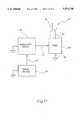
- FIG. 11shows a configuration 63 which incorporates VCSEL 60 of FIG. 4.
- Self-pulsing light 70 of VCSEL 60is frequency modulated with amplitude signals across terminals 50 and 48 from modulator driver 61.
- Modulator driver 61receives signals 69 that are to modulate the self-pulsating light 70 from signal source 67.
- Signals 69having a digital and/or analog format, may originate as signals conveying data, control information, communications and so forth.
- the laser cavity frequency itselfhas been estimated to be in the tens of the GHz regime (at about 50 GHz from the modulation response of the VCSEL shown in FIG. 10.).
- individual VCSELsare inherently extendible to both one and two dimensional arrays permitting easy multiplexing of numerous GHz channels into a 100 plus GHz transmitter in a cost-effective, high yield style.
- Individual elements operating modulation frequency rangecan be controlled by fabrication and/or tuned in operation. The total operating range across the array can be increased by varying each element structure, and also subsequently tuned as discussed previously.
- FIG. 12shows an array 80 of rows or columns of VCSELs having apertures of various sizes.
- VCSELs 81, 82, 83 and 84may have aperture sizes of 10, 20, 30 and 40 microns, and self-pulsation frequencies of 100, 70, 50, and 30 GHz, respectively, for same drive current and electrical power applied to those VCSELs.
- VCSEL 85has the same aperture size as that of VCSEL 81 but a self-pulsation frequency of 120 GHz which is higher than that of VCSEL 81 for the same applied drive current and electrical power.
- the only structural difference between VCSELs 81 and 85is that VCSEL 85 has a dielectric mirror layer that increases the Q of its cavity thereby increasing its self-pulsation frequency.
- FIG. 12may represent an array wherein the phases of each of the VCSELs of array 80 may be controlled relative to one another via current or external delays to result in a VCSEL phased array.
- FIG. 13reveals a cross section of an array of VCSELs having the same structural and electrical characteristics.
- a coating 86 of material having a varying thicknessis applied to the VCSEL array.
- Coating 86has the effect of altering the Q of the VCSEL relative to the thickness of the coating immediately or directly over the respective VCSEL. For example, the greater the thickness of coating 86, the lower the Q of the respective VCSEL as shown by Q's 91 and 92 plotted in graph 89 and positions 87 and 88 of the respective VCSELs.
- a plurality of VCSELsmay be formed into a phased array wherein the phase relationships among the VCSEL outputs are controlled and the outputs can be selectively switched to generate radiator groupings for establishing a particular or desired radiated pattern for a certain direction at a particular frequency.
- controllable mirrormay use any voltage for a controllable effect.
- the lightmay be emitted through either the substrate at one end or the top mirror at the other end.
- verticalis used to mean perpendicular to the major surfaces of the substrate.
- the means for injecting powercan have first and second conductivity types on opposite sides of the active region, either along the axis formed by the first mirror, active region and second mirror, or along some other axis.
Landscapes
- Physics & Mathematics (AREA)
- Condensed Matter Physics & Semiconductors (AREA)
- General Physics & Mathematics (AREA)
- Electromagnetism (AREA)
- Optics & Photonics (AREA)
- Semiconductor Lasers (AREA)
Abstract
Description
dP/dt=Γ.sub.a g.sub.a (n.sub.a -n.sub.0a)P+Γ.sub.s g.sub.s (n.sub.s -n.sub.0s)P-P/τpb+V.sub.a βBn.sub.a.sup.2 (1);
dn.sub.a /dt=-Γ.sub.a g.sub.a (n.sub.a -n.sub.0a)P/V.sub.a +-n.sub.a /τ.sub.a +I.sub.a /eV.sub.a TM (2); and
dn.sub.s /dt=-Γ.sub.s g.sub.s (n.sub.s -n.sub.0s)P/V.sub.s +-n.sub.s /τ.sub.s +(I.sub.s /eV.sub.s) (3);
Claims (12)
Priority Applications (6)
| Application Number | Priority Date | Filing Date | Title |
|---|---|---|---|
| US08/476,965US5574738A (en) | 1995-06-07 | 1995-06-07 | Multi-gigahertz frequency-modulated vertical-cavity surface emitting laser |
| PCT/US1996/007752WO1996041403A1 (en) | 1995-06-07 | 1996-05-28 | Multi-gigahertz frequency-modulated vertical-cavity surface emitting laser |
| EP96921224AEP0830718B1 (en) | 1995-06-07 | 1996-05-28 | Multi-gigahertz frequency-modulated vertical-cavity surface emitting laser |
| JP9500739AJPH11511292A (en) | 1995-06-07 | 1996-05-28 | Multi-gigahertz frequency modulated vertical cavity surface emitting laser |
| CA002221308ACA2221308A1 (en) | 1995-06-07 | 1996-05-28 | Multi-gigahertz frequency-modulated vertical-cavity surface emitting laser |
| DE69610499TDE69610499T2 (en) | 1995-06-07 | 1996-05-28 | MULTI-GIGAHERTZ FREQUENCY MODULATION OF SURFACE-EMITTING LASER WITH VERTICAL RESONATOR |
Applications Claiming Priority (1)
| Application Number | Priority Date | Filing Date | Title |
|---|---|---|---|
| US08/476,965US5574738A (en) | 1995-06-07 | 1995-06-07 | Multi-gigahertz frequency-modulated vertical-cavity surface emitting laser |
Publications (1)
| Publication Number | Publication Date |
|---|---|
| US5574738Atrue US5574738A (en) | 1996-11-12 |
Family
ID=23893951
Family Applications (1)
| Application Number | Title | Priority Date | Filing Date |
|---|---|---|---|
| US08/476,965Expired - LifetimeUS5574738A (en) | 1995-06-07 | 1995-06-07 | Multi-gigahertz frequency-modulated vertical-cavity surface emitting laser |
Country Status (6)
| Country | Link |
|---|---|
| US (1) | US5574738A (en) |
| EP (1) | EP0830718B1 (en) |
| JP (1) | JPH11511292A (en) |
| CA (1) | CA2221308A1 (en) |
| DE (1) | DE69610499T2 (en) |
| WO (1) | WO1996041403A1 (en) |
Cited By (91)
| Publication number | Priority date | Publication date | Assignee | Title |
|---|---|---|---|---|
| US5745152A (en)* | 1994-10-31 | 1998-04-28 | Hewlett Packard Company | Multiple beam laser scanner using lasers with different aperture sizes |
| US5745515A (en)* | 1996-07-18 | 1998-04-28 | Honeywell Inc. | Self-limiting intrinsically eye-safe laser utilizing an increasing absorption layer |
| US5748665A (en)* | 1996-01-16 | 1998-05-05 | Motorola, Inc. | Visible VCSEL with hybrid mirrors |
| US5796771A (en)* | 1996-08-19 | 1998-08-18 | The Regents Of The University Of California | Miniature self-pumped monolithically integrated solid state laser |
| US5892786A (en)* | 1997-03-26 | 1999-04-06 | The United States Of America As Represented By The Secretary Of The Air Force | Output control of vertical microcavity light emitting device |
| US5940422A (en)* | 1996-06-28 | 1999-08-17 | Honeywell Inc. | Laser with an improved mode control |
| US5953362A (en)* | 1997-12-15 | 1999-09-14 | Pamulapati; Jagadeesh | Strain induce control of polarization states in vertical cavity surface emitting lasers and method of making same |
| WO1999057789A1 (en)* | 1998-05-01 | 1999-11-11 | The Regents Of The University Of California | Vertical-cavity surface-emitting laser with an intracavity quantum-well optical absorber |
| US6061380A (en)* | 1997-09-15 | 2000-05-09 | Motorola, Inc. | Vertical cavity surface emitting laser with doped active region and method of fabrication |
| US6064683A (en)* | 1997-12-12 | 2000-05-16 | Honeywell Inc. | Bandgap isolated light emitter |
| WO2000045480A1 (en)* | 1999-02-01 | 2000-08-03 | Gigatera Ag | High-repetition rate passively mode-locked solid-state laser |
| US6327293B1 (en)* | 1998-08-12 | 2001-12-04 | Coherent, Inc. | Optically-pumped external-mirror vertical-cavity semiconductor-laser |
| WO2001095443A1 (en)* | 1999-06-02 | 2001-12-13 | Cielo Communications, Inc. | Single mode vertical cavity surface emitting laser |
| US6393038B1 (en) | 1999-10-04 | 2002-05-21 | Sandia Corporation | Frequency-doubled vertical-external-cavity surface-emitting laser |
| US6412989B1 (en) | 2000-04-10 | 2002-07-02 | Motorola, Inc. | Directable laser transmission module |
| US20020085610A1 (en)* | 2000-12-29 | 2002-07-04 | Morgan Robert A. | Spatially modulated reflector for an optoelectronic device |
| DE10102458A1 (en)* | 2001-01-15 | 2002-07-25 | Infineon Technologies Ag | Laser diode for scanning media has fading absorber means for irradiating a vertical resonator and absorber material integrated into a sequence of layers. |
| US6495381B2 (en)* | 2000-05-18 | 2002-12-17 | Samsung Electronics Co., Ltd. | Apparatus and method for forming aperture of vertical cavity surface emitting laser by selective oxidation |
| US6515305B2 (en) | 2000-09-18 | 2003-02-04 | Regents Of The University Of Minnesota | Vertical cavity surface emitting laser with single mode confinement |
| US20030053503A1 (en)* | 2001-03-07 | 2003-03-20 | Ying-Jay Yang | Device structure for semiconductor lasers |
| US6542527B1 (en) | 1998-08-27 | 2003-04-01 | Regents Of The University Of Minnesota | Vertical cavity surface emitting laser |
| US20030123514A1 (en)* | 2001-12-28 | 2003-07-03 | Cox James A. | Vertical cavity surface emitting laser having a gain guide aperture interior to an oxide confinement layer |
| US20030123502A1 (en)* | 2001-12-28 | 2003-07-03 | Biard James R. | Gain guide implant in oxide vertical cavity surface emitting laser |
| US6594295B1 (en)* | 2001-11-16 | 2003-07-15 | Fox-Tek, Inc. | Semiconductor laser with disordered and non-disordered quantum well regions |
| US20030156611A1 (en)* | 2002-02-21 | 2003-08-21 | Hoki Kwon | GaAs/Al(Ga)As distributed bragg reflector on InP |
| US6611543B2 (en)* | 2000-12-23 | 2003-08-26 | Applied Optoelectronics, Inc. | Vertical-cavity surface-emitting laser with metal mirror and method of fabrication of same |
| US6628695B1 (en) | 2002-03-07 | 2003-09-30 | The Board Of Trustees Of The Leland Stanford Junior University | Monolithically integrated mode-locked vertical cavity surface emitting laser (VCSEL) |
| US6636544B2 (en)* | 2000-12-06 | 2003-10-21 | Applied Optoelectronics, Inc. | Overlapping wavelength-tunable vertical cavity surface-emitting laser (VCSEL) arrays |
| US20030211642A1 (en)* | 2000-08-31 | 2003-11-13 | Honeywell International Inc. | Protective side wall passivation for VCSEL chips |
| US6671304B2 (en) | 2001-08-28 | 2003-12-30 | The United States Of America As Represented By The Secretary Of The Navy | Amplitude-modulated laser for high-bandwidth communications systems |
| WO2002089273A3 (en)* | 2001-03-12 | 2004-01-29 | Honeywell Int Inc | Apparatus and method providing a balancing load to a laser differential drive circuit |
| WO2004021536A1 (en) | 2002-08-28 | 2004-03-11 | Epicrystals Oy | Vertical cavity surface emitting laser comprising a modulator monolithically integrated on top |
| US6751245B1 (en) | 1999-06-02 | 2004-06-15 | Optical Communication Products, Inc. | Single mode vertical cavity surface emitting laser |
| US6798806B1 (en)* | 2002-09-03 | 2004-09-28 | Finisar Corporation | Hybrid mirror VCSELs |
| US6813293B2 (en) | 2002-11-21 | 2004-11-02 | Finisar Corporation | Long wavelength VCSEL with tunnel junction, and implant |
| US20050018714A1 (en)* | 2003-07-25 | 2005-01-27 | Fermann Martin E. | Polarization maintaining dispersion controlled fiber laser source of ultrashort pulses |
| EP1511138A1 (en)* | 2003-09-01 | 2005-03-02 | Avalon Photonics AG | A high power top emitting vertical cavity surface emitting laser |
| KR100475846B1 (en)* | 2001-12-28 | 2005-03-17 | 주식회사 테라스테이트 | Vertical Cavity Surface Emitting Lasers |
| US6882673B1 (en)* | 2001-01-15 | 2005-04-19 | Optical Communication Products, Inc. | Mirror structure for reducing the effect of feedback on a VCSEL |
| US6887801B2 (en) | 2003-07-18 | 2005-05-03 | Finisar Corporation | Edge bead control method and apparatus |
| US20050117623A1 (en)* | 2003-12-01 | 2005-06-02 | Nl-Nanosemiconductor Gmbh | Optoelectronic device incorporating an interference filter |
| US6905900B1 (en) | 2000-11-28 | 2005-06-14 | Finisar Corporation | Versatile method and system for single mode VCSELs |
| US20050190812A1 (en)* | 2002-10-28 | 2005-09-01 | Johnson Ralph H. | Distributed bragg reflector for optoelectronic device |
| WO2005098573A1 (en)* | 2004-03-31 | 2005-10-20 | Intel Corporation | Surface emitting laser with an integrated absorber |
| US6961489B2 (en) | 2003-06-30 | 2005-11-01 | Finisar Corporation | High speed optical system |
| US6965626B2 (en)* | 2002-09-03 | 2005-11-15 | Finisar Corporation | Single mode VCSEL |
| US20050259916A1 (en)* | 2003-05-21 | 2005-11-24 | David Jenkins | Multimode fiber optical fiber transmission system with offset launch single mode long wavelength vertical cavity surface emitting laser transmitter |
| US20050271092A1 (en)* | 2004-06-07 | 2005-12-08 | Nl-Nanosemiconductor Gmbh | Electrooptically wavelength-tunable resonant cavity optoelectronic device for high-speed data transfer |
| US20060043278A1 (en)* | 2004-08-30 | 2006-03-02 | Honeywell International Inc. | VCSEL pin sensor |
| US7031363B2 (en) | 2003-10-29 | 2006-04-18 | Finisar Corporation | Long wavelength VCSEL device processing |
| US7054345B2 (en) | 2003-06-27 | 2006-05-30 | Finisar Corporation | Enhanced lateral oxidation |
| US20060124829A1 (en)* | 2004-12-10 | 2006-06-15 | Song Hyun W | Surface emitting laser device including optical sensor and optical waveguide device employing the same |
| US7065124B2 (en) | 2000-11-28 | 2006-06-20 | Finlsar Corporation | Electron affinity engineered VCSELs |
| US7075962B2 (en) | 2003-06-27 | 2006-07-11 | Finisar Corporation | VCSEL having thermal management |
| US7149383B2 (en) | 2003-06-30 | 2006-12-12 | Finisar Corporation | Optical system with reduced back reflection |
| US20060291515A1 (en)* | 2005-06-28 | 2006-12-28 | Samsung Electronics Co., Ltd. | High power vertical external cavity surface emitting laser |
| US20070063140A1 (en)* | 2005-09-22 | 2007-03-22 | Honeywell International Inc. | Optical particulate sensor in oil quality detection |
| US7210857B2 (en) | 2003-07-16 | 2007-05-01 | Finisar Corporation | Optical coupling system |
| US7277461B2 (en)* | 2003-06-27 | 2007-10-02 | Finisar Corporation | Dielectric VCSEL gain guide |
| US7298942B2 (en) | 2003-06-06 | 2007-11-20 | Finisar Corporation | Pluggable optical optic system having a lens fiber stop |
| US20070291799A1 (en)* | 2006-06-16 | 2007-12-20 | Janne Konttinen | High power laser device |
| US20080131051A1 (en)* | 2004-05-22 | 2008-06-05 | Ocp-Europe, Ltd. | Multi-mode fiber, optical fiber transmission system with offset-launch, single-mode, long-wavelength, vertical cavity surface emitting laser transmitter |
| US7433381B2 (en) | 2003-06-25 | 2008-10-07 | Finisar Corporation | InP based long wavelength VCSEL |
| US20080267231A1 (en)* | 2007-04-30 | 2008-10-30 | The Research Foundation Of State University Of New York | Detuned duo-cavity laser-modulator device and method with detuning selected to minimize change in reflectivity |
| US20090041464A1 (en)* | 2007-08-10 | 2009-02-12 | Vi Systems Gmbh | Anti Stark Electrooptic Medium and Electrooptically Modulated Optoelectronic Device Based Thereupon |
| US7596165B2 (en) | 2004-08-31 | 2009-09-29 | Finisar Corporation | Distributed Bragg Reflector for optoelectronic device |
| US20090296754A1 (en)* | 2006-06-16 | 2009-12-03 | Vi Systems Gmbh | Optoelectric Device for High-Speed Data Transfer with Electrooptically Tunable Stopband Edge of a Bragg-Reflector |
| CN1813339B (en)* | 2003-06-30 | 2010-10-13 | 电子科学工业公司 | Laser pulse selection with controlled acousto-optic modulator loading |
| US7829912B2 (en) | 2006-07-31 | 2010-11-09 | Finisar Corporation | Efficient carrier injection in a semiconductor device |
| US7920612B2 (en) | 2004-08-31 | 2011-04-05 | Finisar Corporation | Light emitting semiconductor device having an electrical confinement barrier near the active region |
| US20110148328A1 (en)* | 2009-12-19 | 2011-06-23 | Trilumina Corporation | System and method for combining laser arrays for digital outputs |
| US20110181942A1 (en)* | 2008-05-23 | 2011-07-28 | Hila Hashemi | Nonlinear harmonic generation and devices in doubly-resonant kerr cavities |
| US8031752B1 (en) | 2007-04-16 | 2011-10-04 | Finisar Corporation | VCSEL optimized for high speed data |
| US20120075634A1 (en)* | 2010-09-27 | 2012-03-29 | Stichting Imec Nederland | Sensor, Method for Detecting The Presence and/or Concentration of an Analyte Using the Sensor, and Use of the Method |
| US8208196B2 (en) | 2003-07-25 | 2012-06-26 | Imra America, Inc. | Pulsed laser sources |
| US8406266B2 (en) | 2011-08-31 | 2013-03-26 | Avago Technologies Fiber Ip (Singapore) Pte. Ltd | Three-terminal vertical cavity surface emitting laser (VCSEL) and a method for operating a three-terminal VCSEL |
| US8687983B2 (en) | 2011-11-02 | 2014-04-01 | Hewlett-Packard Development Company, L.P. | Laser communication system |
| US8979338B2 (en) | 2009-12-19 | 2015-03-17 | Trilumina Corp. | System for combining laser array outputs into a single beam carrying digital data |
| US8995485B2 (en) | 2009-02-17 | 2015-03-31 | Trilumina Corp. | High brightness pulsed VCSEL sources |
| US8995493B2 (en) | 2009-02-17 | 2015-03-31 | Trilumina Corp. | Microlenses for multibeam arrays of optoelectronic devices for high frequency operation |
| US9071037B2 (en) | 2004-03-31 | 2015-06-30 | Imra America, Inc. | High power short pulse fiber laser |
| US9190810B2 (en) | 2008-07-28 | 2015-11-17 | Avago Technologies General Ip (Singapore) Pte. Ltd. | Three-terminal vertical cavity surface emitting laser (VCSEL) and a method for operating a three-terminal VCSEL |
| US10038304B2 (en) | 2009-02-17 | 2018-07-31 | Trilumina Corp. | Laser arrays for variable optical properties |
| US10244181B2 (en) | 2009-02-17 | 2019-03-26 | Trilumina Corp. | Compact multi-zone infrared laser illuminator |
| DE102018003982A1 (en)* | 2018-05-17 | 2019-11-21 | 3-5 Power Electronics GmbH | Semiconductor device manufacturing method and semiconductor device |
| US10615871B2 (en) | 2009-02-17 | 2020-04-07 | Trilumina Corp. | High speed free-space optical communications |
| US10707650B2 (en) | 2016-03-04 | 2020-07-07 | Princeton Optronics, Inc. | High-speed VCSEL device |
| US10739137B2 (en) | 2018-08-17 | 2020-08-11 | Honeywell International Inc. | Solid state ring laser gyroscope using rare-earth gain dopants in glassy hosts |
| US20210028603A1 (en)* | 2018-04-04 | 2021-01-28 | Lg Innotek Co., Ltd. | A surface-emitting laser device and light emitting device including the same |
| US11095365B2 (en) | 2011-08-26 | 2021-08-17 | Lumentum Operations Llc | Wide-angle illuminator module |
| US11962118B2 (en) | 2020-10-27 | 2024-04-16 | Honeywell International Inc. | Ultraviolet filter for ring laser gyroscope mirrors |
Families Citing this family (3)
| Publication number | Priority date | Publication date | Assignee | Title |
|---|---|---|---|---|
| DE10129616A1 (en)* | 2001-06-20 | 2003-01-09 | Infineon Technologies Ag | Solid state laser based upon a pair of coupled lasers and a means for coupling emissions |
| JP7646596B2 (en)* | 2021-05-17 | 2025-03-17 | キヤノン株式会社 | Light emitting device and distance measuring device |
| JP2023028421A (en)* | 2021-08-19 | 2023-03-03 | キヤノン株式会社 | Light source device and ranging device |
Citations (5)
| Publication number | Priority date | Publication date | Assignee | Title |
|---|---|---|---|---|
| US4885592A (en)* | 1987-12-28 | 1989-12-05 | Kofol J Stephen | Electronically steerable antenna |
| US5056098A (en)* | 1990-07-05 | 1991-10-08 | At&T Bell Laboratories | Vertical cavity laser with mirror having controllable reflectivity |
| US5115442A (en)* | 1990-04-13 | 1992-05-19 | At&T Bell Laboratories | Top-emitting surface emitting laser structures |
| US5206872A (en)* | 1991-11-01 | 1993-04-27 | At&T Bell Laboratories | Surface emitting laser |
| US5359447A (en)* | 1993-06-25 | 1994-10-25 | Hewlett-Packard Company | Optical communication with vertical-cavity surface-emitting laser operating in multiple transverse modes |
Family Cites Families (1)
| Publication number | Priority date | Publication date | Assignee | Title |
|---|---|---|---|---|
| US5040183A (en)* | 1990-07-20 | 1991-08-13 | At&T Bell Laboratories | Apparatus comprising optical pulse-generating means |
- 1995
- 1995-06-07USUS08/476,965patent/US5574738A/ennot_activeExpired - Lifetime
- 1996
- 1996-05-28WOPCT/US1996/007752patent/WO1996041403A1/enactiveIP Right Grant
- 1996-05-28JPJP9500739Apatent/JPH11511292A/ennot_activeCeased
- 1996-05-28EPEP96921224Apatent/EP0830718B1/ennot_activeExpired - Lifetime
- 1996-05-28CACA002221308Apatent/CA2221308A1/ennot_activeAbandoned
- 1996-05-28DEDE69610499Tpatent/DE69610499T2/ennot_activeExpired - Lifetime
Patent Citations (5)
| Publication number | Priority date | Publication date | Assignee | Title |
|---|---|---|---|---|
| US4885592A (en)* | 1987-12-28 | 1989-12-05 | Kofol J Stephen | Electronically steerable antenna |
| US5115442A (en)* | 1990-04-13 | 1992-05-19 | At&T Bell Laboratories | Top-emitting surface emitting laser structures |
| US5056098A (en)* | 1990-07-05 | 1991-10-08 | At&T Bell Laboratories | Vertical cavity laser with mirror having controllable reflectivity |
| US5206872A (en)* | 1991-11-01 | 1993-04-27 | At&T Bell Laboratories | Surface emitting laser |
| US5359447A (en)* | 1993-06-25 | 1994-10-25 | Hewlett-Packard Company | Optical communication with vertical-cavity surface-emitting laser operating in multiple transverse modes |
Non-Patent Citations (16)
| Title |
|---|
| D. Chemia et al., Chapter 4 "Nonlinear Optical Properties of Semiconductor Quantum Wells," 1988, Optical Nonlinearities and Instabilities in Semiconductors, pp. 83-120. (No Month). |
| D. Chemia et al., Chapter 4 Nonlinear Optical Properties of Semiconductor Quantum Wells, 1988, Optical Nonlinearities and Instabilities in Semiconductors, pp. 83 120. (No Month).* |
| D. Nugent et al., "Self-pulsations in vertical-cavity surface-emitting lasers," Jan. 5, 1995, Electronics Letters. |
| D. Nugent et al., Self pulsations in vertical cavity surface emitting lasers, Jan. 5, 1995, Electronics Letters.* |
| F. Choa et al., "High-Speed Modulation of Vertical-Cavity Surface-Emitting Lasers," Aug. 1991, IEEE Photonics Technology Letters, vol. 3, No. 8, pp. 697-699. |
| F. Choa et al., High Speed Modulation of Vertical Cavity Surface Emitting Lasers, Aug. 1991, IEEE Photonics Technology Letters, vol. 3, No. 8, pp. 697 699.* |
| J. Jewell et al., "Surface-emitting microlasers for photonic switching and interchip connections," Mar. 1990, Optical Engineering, vol. 29, No. 3. |
| J. Jewell et al., Surface emitting microlasers for photonic switching and interchip connections, Mar. 1990, Optical Engineering, vol. 29, No. 3.* |
| R. Morgan et al., "Vertical-cavity surface-emitting laser arrays," (1995) SPIE, vol. 2398-09, Bellingham WA. (No Month). |
| R. Morgan et al., Vertical cavity surface emitting laser arrays, (1995) SPIE, vol. 2398 09, Bellingham WA. (No Month).* |
| S. Jiang et al., "High-frequency polarization self-modulation in vertical-cavity surface-emitting lasers," Dec. 27, 1993, Applied Physics Letters, pp. 3545-3547. |
| S. Jiang et al., High frequency polarization self modulation in vertical cavity surface emitting lasers, Dec. 27, 1993, Applied Physics Letters, pp. 3545 3547.* |
| T. Banweil et al., "VCSE Laser Transmitters for Parallel Data Links," Feb. 1993, IEEE Journal of Quantum Electronics, vol. 29, No. 2, pp. 635-644. |
| T. Banweil et al., VCSE Laser Transmitters for Parallel Data Links, Feb. 1993, IEEE Journal of Quantum Electronics, vol. 29, No. 2, pp. 635 644.* |
| Y. Lee et al., "Top-Surface-Emitting GaAs Four-Quantum-Will Lasers Emitting at 0.85μm," May 24, 1990,, Electronics Letters. |
| Y. Lee et al., Top Surface Emitting GaAs Four Quantum Will Lasers Emitting at 0.85 m, May 24, 1990,, Electronics Letters.* |
Cited By (152)
| Publication number | Priority date | Publication date | Assignee | Title |
|---|---|---|---|---|
| US5745152A (en)* | 1994-10-31 | 1998-04-28 | Hewlett Packard Company | Multiple beam laser scanner using lasers with different aperture sizes |
| US5748665A (en)* | 1996-01-16 | 1998-05-05 | Motorola, Inc. | Visible VCSEL with hybrid mirrors |
| US5940422A (en)* | 1996-06-28 | 1999-08-17 | Honeywell Inc. | Laser with an improved mode control |
| US5745515A (en)* | 1996-07-18 | 1998-04-28 | Honeywell Inc. | Self-limiting intrinsically eye-safe laser utilizing an increasing absorption layer |
| US5796771A (en)* | 1996-08-19 | 1998-08-18 | The Regents Of The University Of California | Miniature self-pumped monolithically integrated solid state laser |
| US6026108A (en)* | 1996-10-16 | 2000-02-15 | The Regents Of The University Of California | Vertical-cavity surface-emitting laser with an intracavity quantum-well optical absorber |
| US5892786A (en)* | 1997-03-26 | 1999-04-06 | The United States Of America As Represented By The Secretary Of The Air Force | Output control of vertical microcavity light emitting device |
| US6061380A (en)* | 1997-09-15 | 2000-05-09 | Motorola, Inc. | Vertical cavity surface emitting laser with doped active region and method of fabrication |
| US6064683A (en)* | 1997-12-12 | 2000-05-16 | Honeywell Inc. | Bandgap isolated light emitter |
| US5953362A (en)* | 1997-12-15 | 1999-09-14 | Pamulapati; Jagadeesh | Strain induce control of polarization states in vertical cavity surface emitting lasers and method of making same |
| WO1999057789A1 (en)* | 1998-05-01 | 1999-11-11 | The Regents Of The University Of California | Vertical-cavity surface-emitting laser with an intracavity quantum-well optical absorber |
| US6327293B1 (en)* | 1998-08-12 | 2001-12-04 | Coherent, Inc. | Optically-pumped external-mirror vertical-cavity semiconductor-laser |
| US6542527B1 (en) | 1998-08-27 | 2003-04-01 | Regents Of The University Of Minnesota | Vertical cavity surface emitting laser |
| WO2000045480A1 (en)* | 1999-02-01 | 2000-08-03 | Gigatera Ag | High-repetition rate passively mode-locked solid-state laser |
| US6751245B1 (en) | 1999-06-02 | 2004-06-15 | Optical Communication Products, Inc. | Single mode vertical cavity surface emitting laser |
| WO2001095443A1 (en)* | 1999-06-02 | 2001-12-13 | Cielo Communications, Inc. | Single mode vertical cavity surface emitting laser |
| US6393038B1 (en) | 1999-10-04 | 2002-05-21 | Sandia Corporation | Frequency-doubled vertical-external-cavity surface-emitting laser |
| US6412989B1 (en) | 2000-04-10 | 2002-07-02 | Motorola, Inc. | Directable laser transmission module |
| US6495381B2 (en)* | 2000-05-18 | 2002-12-17 | Samsung Electronics Co., Ltd. | Apparatus and method for forming aperture of vertical cavity surface emitting laser by selective oxidation |
| US6924161B2 (en) | 2000-08-31 | 2005-08-02 | Finisar Corporation | Protective side wall passivation for VCSEL chips |
| US20030211642A1 (en)* | 2000-08-31 | 2003-11-13 | Honeywell International Inc. | Protective side wall passivation for VCSEL chips |
| US6674777B1 (en) | 2000-08-31 | 2004-01-06 | Honeywell International Inc. | Protective side wall passivation for VCSEL chips |
| US6515305B2 (en) | 2000-09-18 | 2003-02-04 | Regents Of The University Of Minnesota | Vertical cavity surface emitting laser with single mode confinement |
| US6905900B1 (en) | 2000-11-28 | 2005-06-14 | Finisar Corporation | Versatile method and system for single mode VCSELs |
| US7221691B2 (en) | 2000-11-28 | 2007-05-22 | Finisar Corporation | Versatile method and system for single mode VCSELs |
| US7065124B2 (en) | 2000-11-28 | 2006-06-20 | Finlsar Corporation | Electron affinity engineered VCSELs |
| US7308011B2 (en) | 2000-11-28 | 2007-12-11 | Finisar Corporation | Versatile method and system for single mode VCSELs |
| US6636544B2 (en)* | 2000-12-06 | 2003-10-21 | Applied Optoelectronics, Inc. | Overlapping wavelength-tunable vertical cavity surface-emitting laser (VCSEL) arrays |
| US6611543B2 (en)* | 2000-12-23 | 2003-08-26 | Applied Optoelectronics, Inc. | Vertical-cavity surface-emitting laser with metal mirror and method of fabrication of same |
| US6727520B2 (en) | 2000-12-29 | 2004-04-27 | Honeywell International Inc. | Spatially modulated reflector for an optoelectronic device |
| US20040188695A1 (en)* | 2000-12-29 | 2004-09-30 | Morgan Robert A. | Laser with resonant reflector |
| US7760786B2 (en) | 2000-12-29 | 2010-07-20 | Finisar Corporation | Laser with resonant reflector |
| US20020085610A1 (en)* | 2000-12-29 | 2002-07-04 | Morgan Robert A. | Spatially modulated reflector for an optoelectronic device |
| US7266135B2 (en) | 2000-12-29 | 2007-09-04 | Finisar Corporation | Method for producing laser with resonant reflector |
| US20040191941A1 (en)* | 2000-12-29 | 2004-09-30 | Morgan Robert A. | Method for producing laser with resonant reflector |
| DE10102458A1 (en)* | 2001-01-15 | 2002-07-25 | Infineon Technologies Ag | Laser diode for scanning media has fading absorber means for irradiating a vertical resonator and absorber material integrated into a sequence of layers. |
| US20050100063A1 (en)* | 2001-01-15 | 2005-05-12 | Optical Communication Products, Inc. | Mirror structure for reducing the effect of feedback on a VCSEL |
| US6882673B1 (en)* | 2001-01-15 | 2005-04-19 | Optical Communication Products, Inc. | Mirror structure for reducing the effect of feedback on a VCSEL |
| US6990127B2 (en) | 2001-01-15 | 2006-01-24 | Infineon Technologies Ag | Vertical laser diode with means for beam profile forming |
| US20030053503A1 (en)* | 2001-03-07 | 2003-03-20 | Ying-Jay Yang | Device structure for semiconductor lasers |
| US6728280B1 (en) | 2001-03-12 | 2004-04-27 | Honeywell International Inc. | Apparatus and method providing a balancing load to a laser differential drive circuit |
| WO2002089273A3 (en)* | 2001-03-12 | 2004-01-29 | Honeywell Int Inc | Apparatus and method providing a balancing load to a laser differential drive circuit |
| US6671304B2 (en) | 2001-08-28 | 2003-12-30 | The United States Of America As Represented By The Secretary Of The Navy | Amplitude-modulated laser for high-bandwidth communications systems |
| US6594295B1 (en)* | 2001-11-16 | 2003-07-15 | Fox-Tek, Inc. | Semiconductor laser with disordered and non-disordered quantum well regions |
| KR100475846B1 (en)* | 2001-12-28 | 2005-03-17 | 주식회사 테라스테이트 | Vertical Cavity Surface Emitting Lasers |
| US6904072B2 (en)* | 2001-12-28 | 2005-06-07 | Finisar Corporation | Vertical cavity surface emitting laser having a gain guide aperture interior to an oxide confinement layer |
| US20030123502A1 (en)* | 2001-12-28 | 2003-07-03 | Biard James R. | Gain guide implant in oxide vertical cavity surface emitting laser |
| US20050233486A1 (en)* | 2001-12-28 | 2005-10-20 | Finisar Corporation | Vertical cavity surface emitting laser having a gain guide aperture interior to an oxide confinement layer |
| US20050018729A1 (en)* | 2001-12-28 | 2005-01-27 | Biard James R. | Implant damaged oxide insulating region in vertical cavity surface emitting laser |
| US20030123514A1 (en)* | 2001-12-28 | 2003-07-03 | Cox James A. | Vertical cavity surface emitting laser having a gain guide aperture interior to an oxide confinement layer |
| US6816526B2 (en)* | 2001-12-28 | 2004-11-09 | Finisar Corporation | Gain guide implant in oxide vertical cavity surface emitting laser |
| US7432118B2 (en) | 2001-12-28 | 2008-10-07 | Finisar Corporation | Vertical cavity surface emitting laser having a gain guide aperture interior to an oxide confinement layer |
| US7095771B2 (en) | 2001-12-28 | 2006-08-22 | Finisar Corporation | Implant damaged oxide insulating region in vertical cavity surface emitting laser |
| US6822995B2 (en)* | 2002-02-21 | 2004-11-23 | Finisar Corporation | GaAs/AI(Ga)As distributed bragg reflector on InP |
| US20030156611A1 (en)* | 2002-02-21 | 2003-08-21 | Hoki Kwon | GaAs/Al(Ga)As distributed bragg reflector on InP |
| US6628695B1 (en) | 2002-03-07 | 2003-09-30 | The Board Of Trustees Of The Leland Stanford Junior University | Monolithically integrated mode-locked vertical cavity surface emitting laser (VCSEL) |
| WO2004021536A1 (en) | 2002-08-28 | 2004-03-11 | Epicrystals Oy | Vertical cavity surface emitting laser comprising a modulator monolithically integrated on top |
| US7110427B2 (en)* | 2002-09-03 | 2006-09-19 | Finisar Corporation | Hybrid mirror VCSEL |
| US6798806B1 (en)* | 2002-09-03 | 2004-09-28 | Finisar Corporation | Hybrid mirror VCSELs |
| US6965626B2 (en)* | 2002-09-03 | 2005-11-15 | Finisar Corporation | Single mode VCSEL |
| US20050047474A1 (en)* | 2002-09-03 | 2005-03-03 | Finisar | Hybrid mirror VCSEL |
| US20050190812A1 (en)* | 2002-10-28 | 2005-09-01 | Johnson Ralph H. | Distributed bragg reflector for optoelectronic device |
| US7251264B2 (en) | 2002-10-28 | 2007-07-31 | Finisar Corporation | Distributed bragg reflector for optoelectronic device |
| US6990135B2 (en) | 2002-10-28 | 2006-01-24 | Finisar Corporation | Distributed bragg reflector for optoelectronic device |
| US6813293B2 (en) | 2002-11-21 | 2004-11-02 | Finisar Corporation | Long wavelength VCSEL with tunnel junction, and implant |
| US7231114B2 (en) | 2003-05-21 | 2007-06-12 | Ocp-Europe, Ltd. | Multimode fiber optical fiber transmission system with offset launch single mode long wavelength vertical cavity surface emitting laser transmitter |
| US20050259916A1 (en)* | 2003-05-21 | 2005-11-24 | David Jenkins | Multimode fiber optical fiber transmission system with offset launch single mode long wavelength vertical cavity surface emitting laser transmitter |
| US7298942B2 (en) | 2003-06-06 | 2007-11-20 | Finisar Corporation | Pluggable optical optic system having a lens fiber stop |
| US7433381B2 (en) | 2003-06-25 | 2008-10-07 | Finisar Corporation | InP based long wavelength VCSEL |
| US7277461B2 (en)* | 2003-06-27 | 2007-10-02 | Finisar Corporation | Dielectric VCSEL gain guide |
| US7054345B2 (en) | 2003-06-27 | 2006-05-30 | Finisar Corporation | Enhanced lateral oxidation |
| US7075962B2 (en) | 2003-06-27 | 2006-07-11 | Finisar Corporation | VCSEL having thermal management |
| US7149383B2 (en) | 2003-06-30 | 2006-12-12 | Finisar Corporation | Optical system with reduced back reflection |
| CN1813339B (en)* | 2003-06-30 | 2010-10-13 | 电子科学工业公司 | Laser pulse selection with controlled acousto-optic modulator loading |
| US7139454B2 (en) | 2003-06-30 | 2006-11-21 | Finisar Corporation | Methods for signal transmission in optical fiber |
| US6961489B2 (en) | 2003-06-30 | 2005-11-01 | Finisar Corporation | High speed optical system |
| US7210857B2 (en) | 2003-07-16 | 2007-05-01 | Finisar Corporation | Optical coupling system |
| US6887801B2 (en) | 2003-07-18 | 2005-05-03 | Finisar Corporation | Edge bead control method and apparatus |
| US8456735B2 (en) | 2003-07-25 | 2013-06-04 | Imra America, Inc. | Pulsed laser sources |
| US7088756B2 (en)* | 2003-07-25 | 2006-08-08 | Imra America, Inc. | Polarization maintaining dispersion controlled fiber laser source of ultrashort pulses |
| US9653868B2 (en) | 2003-07-25 | 2017-05-16 | Imra America, Inc. | Pulsed laser sources |
| US8208196B2 (en) | 2003-07-25 | 2012-06-26 | Imra America, Inc. | Pulsed laser sources |
| US20050018714A1 (en)* | 2003-07-25 | 2005-01-27 | Fermann Martin E. | Polarization maintaining dispersion controlled fiber laser source of ultrashort pulses |
| US9401579B2 (en) | 2003-07-25 | 2016-07-26 | Imra America, Inc. | Pulsed laser sources |
| US8599473B2 (en) | 2003-07-25 | 2013-12-03 | Imra America, Inc. | Pulsed laser sources |
| US20070091960A1 (en)* | 2003-09-01 | 2007-04-26 | Hans-Peter Gauggel | High power top emitting vertical cavity surface emitting laser |
| US8247252B2 (en) | 2003-09-01 | 2012-08-21 | Oclaro Technology Limited | High power top emitting vertical cavity surface emitting laser |
| EP1511138A1 (en)* | 2003-09-01 | 2005-03-02 | Avalon Photonics AG | A high power top emitting vertical cavity surface emitting laser |
| WO2005022712A1 (en)* | 2003-09-01 | 2005-03-10 | Avalon Photonics Ag | A high power top emitting vertical cavity surface emitting laser |
| US20100035372A1 (en)* | 2003-09-01 | 2010-02-11 | Avalon Photonics Ag | High power top emitting vertical cavity surface emitting laser |
| US7031363B2 (en) | 2003-10-29 | 2006-04-18 | Finisar Corporation | Long wavelength VCSEL device processing |
| US20050117623A1 (en)* | 2003-12-01 | 2005-06-02 | Nl-Nanosemiconductor Gmbh | Optoelectronic device incorporating an interference filter |
| US20070189350A1 (en)* | 2004-03-31 | 2007-08-16 | Young Ian A | Surface emitting laser with an integrated absorber |
| CN1950781B (en)* | 2004-03-31 | 2011-04-20 | 英特尔公司 | Surface-emitting lasers with integrated absorbers |
| US20060029112A1 (en)* | 2004-03-31 | 2006-02-09 | Young Ian A | Surface emitting laser with an integrated absorber |
| US9640940B2 (en) | 2004-03-31 | 2017-05-02 | Imra America, Inc. | High power short pulse fiber laser |
| WO2005098573A1 (en)* | 2004-03-31 | 2005-10-20 | Intel Corporation | Surface emitting laser with an integrated absorber |
| US9071037B2 (en) | 2004-03-31 | 2015-06-30 | Imra America, Inc. | High power short pulse fiber laser |
| US7729393B2 (en) | 2004-03-31 | 2010-06-01 | Intel Corporation | Surface emitting laser with an integrated absorber |
| US7477815B2 (en) | 2004-05-22 | 2009-01-13 | Ocp-Europe, Ltd | Multi-mode fiber, optical fiber transmission system with offset-launch, single-mode, long-wavelength, vertical cavity surface emitting laser transmitter |
| US20080131051A1 (en)* | 2004-05-22 | 2008-06-05 | Ocp-Europe, Ltd. | Multi-mode fiber, optical fiber transmission system with offset-launch, single-mode, long-wavelength, vertical cavity surface emitting laser transmitter |
| US7369583B2 (en) | 2004-06-07 | 2008-05-06 | Innolume Gmbh | Electrooptically wavelength-tunable resonant cavity optoelectronic device for high-speed data transfer |
| US20050271092A1 (en)* | 2004-06-07 | 2005-12-08 | Nl-Nanosemiconductor Gmbh | Electrooptically wavelength-tunable resonant cavity optoelectronic device for high-speed data transfer |
| US20060043278A1 (en)* | 2004-08-30 | 2006-03-02 | Honeywell International Inc. | VCSEL pin sensor |
| US7596165B2 (en) | 2004-08-31 | 2009-09-29 | Finisar Corporation | Distributed Bragg Reflector for optoelectronic device |
| US7920612B2 (en) | 2004-08-31 | 2011-04-05 | Finisar Corporation | Light emitting semiconductor device having an electrical confinement barrier near the active region |
| US20060124829A1 (en)* | 2004-12-10 | 2006-06-15 | Song Hyun W | Surface emitting laser device including optical sensor and optical waveguide device employing the same |
| US7244923B2 (en) | 2004-12-10 | 2007-07-17 | Electronics And Telecommunications Research Institute | Surface emitting laser device including optical sensor and optical waveguide device employing the same |
| US7684454B2 (en)* | 2005-06-28 | 2010-03-23 | Samsung Electronics Co., Ltd. | High power vertical cavity surface emitting laser |
| US20060291515A1 (en)* | 2005-06-28 | 2006-12-28 | Samsung Electronics Co., Ltd. | High power vertical external cavity surface emitting laser |
| US7321117B2 (en) | 2005-09-22 | 2008-01-22 | Honeywell International Inc. | Optical particulate sensor in oil quality detection |
| US20070063140A1 (en)* | 2005-09-22 | 2007-03-22 | Honeywell International Inc. | Optical particulate sensor in oil quality detection |
| US20090296754A1 (en)* | 2006-06-16 | 2009-12-03 | Vi Systems Gmbh | Optoelectric Device for High-Speed Data Transfer with Electrooptically Tunable Stopband Edge of a Bragg-Reflector |
| US7801197B2 (en) | 2006-06-16 | 2010-09-21 | Epicrystals Oy | High power laser device |
| US20070291799A1 (en)* | 2006-06-16 | 2007-12-20 | Janne Konttinen | High power laser device |
| WO2007144471A1 (en)* | 2006-06-16 | 2007-12-21 | Epicrystals Oy | High power laser device |
| US8290016B2 (en) | 2006-06-16 | 2012-10-16 | Connector Optics | Optoelectric device for high-speed data transfer with electrooptically tunable stopband edge of a bragg-reflector |
| EP2041849A4 (en)* | 2006-06-16 | 2010-04-21 | Epicrystals Oy | High power laser device |
| US7829912B2 (en) | 2006-07-31 | 2010-11-09 | Finisar Corporation | Efficient carrier injection in a semiconductor device |
| US8031752B1 (en) | 2007-04-16 | 2011-10-04 | Finisar Corporation | VCSEL optimized for high speed data |
| US20080267231A1 (en)* | 2007-04-30 | 2008-10-30 | The Research Foundation Of State University Of New York | Detuned duo-cavity laser-modulator device and method with detuning selected to minimize change in reflectivity |
| US7508858B2 (en) | 2007-04-30 | 2009-03-24 | The Research Foundation Of State University Of New York | Detuned duo-cavity laser-modulator device and method with detuning selected to minimize change in reflectivity |
| US7772615B2 (en) | 2007-08-10 | 2010-08-10 | Connector Optics | Anti stark electrooptic medium and electrooptically modulated optoelectronic device based thereupon |
| US20090041464A1 (en)* | 2007-08-10 | 2009-02-12 | Vi Systems Gmbh | Anti Stark Electrooptic Medium and Electrooptically Modulated Optoelectronic Device Based Thereupon |
| US8045257B2 (en) | 2008-05-23 | 2011-10-25 | Massachusetts Institute Of Technology | Nonlinear harmonic generation and devices in doubly-resonant Kerr cavities |
| US20110181942A1 (en)* | 2008-05-23 | 2011-07-28 | Hila Hashemi | Nonlinear harmonic generation and devices in doubly-resonant kerr cavities |
| US9190810B2 (en) | 2008-07-28 | 2015-11-17 | Avago Technologies General Ip (Singapore) Pte. Ltd. | Three-terminal vertical cavity surface emitting laser (VCSEL) and a method for operating a three-terminal VCSEL |
| US10938476B2 (en) | 2009-02-17 | 2021-03-02 | Lumentum Operations Llc | System for optical free-space transmission of a string of binary data |
| US10615871B2 (en) | 2009-02-17 | 2020-04-07 | Trilumina Corp. | High speed free-space optical communications |
| US8995485B2 (en) | 2009-02-17 | 2015-03-31 | Trilumina Corp. | High brightness pulsed VCSEL sources |
| US8995493B2 (en) | 2009-02-17 | 2015-03-31 | Trilumina Corp. | Microlenses for multibeam arrays of optoelectronic devices for high frequency operation |
| US10038304B2 (en) | 2009-02-17 | 2018-07-31 | Trilumina Corp. | Laser arrays for variable optical properties |
| US11075695B2 (en) | 2009-02-17 | 2021-07-27 | Lumentum Operations Llc | Eye-safe optical laser system |
| US11121770B2 (en) | 2009-02-17 | 2021-09-14 | Lumentum Operations Llc | Optical laser device |
| US10244181B2 (en) | 2009-02-17 | 2019-03-26 | Trilumina Corp. | Compact multi-zone infrared laser illuminator |
| US11405105B2 (en) | 2009-02-17 | 2022-08-02 | Lumentum Operations Llc | System for optical free-space transmission of a string of binary data |
| US8979338B2 (en) | 2009-12-19 | 2015-03-17 | Trilumina Corp. | System for combining laser array outputs into a single beam carrying digital data |
| US20110148328A1 (en)* | 2009-12-19 | 2011-06-23 | Trilumina Corporation | System and method for combining laser arrays for digital outputs |
| US8613536B2 (en) | 2009-12-19 | 2013-12-24 | Trilumina Corporation | System and method for combining laser arrays for digital outputs |
| US8634078B2 (en)* | 2010-09-27 | 2014-01-21 | Stichting Imec Nederland | Sensor, method for detecting the presence and/or concentration of an analyte using the sensor, and use of the method |
| US20120075634A1 (en)* | 2010-09-27 | 2012-03-29 | Stichting Imec Nederland | Sensor, Method for Detecting The Presence and/or Concentration of an Analyte Using the Sensor, and Use of the Method |
| US11451013B2 (en) | 2011-08-26 | 2022-09-20 | Lumentum Operations Llc | Wide-angle illuminator module |
| US11095365B2 (en) | 2011-08-26 | 2021-08-17 | Lumentum Operations Llc | Wide-angle illuminator module |
| US8406266B2 (en) | 2011-08-31 | 2013-03-26 | Avago Technologies Fiber Ip (Singapore) Pte. Ltd | Three-terminal vertical cavity surface emitting laser (VCSEL) and a method for operating a three-terminal VCSEL |
| US8687983B2 (en) | 2011-11-02 | 2014-04-01 | Hewlett-Packard Development Company, L.P. | Laser communication system |
| US10707650B2 (en) | 2016-03-04 | 2020-07-07 | Princeton Optronics, Inc. | High-speed VCSEL device |
| US20210028603A1 (en)* | 2018-04-04 | 2021-01-28 | Lg Innotek Co., Ltd. | A surface-emitting laser device and light emitting device including the same |
| US11942762B2 (en)* | 2018-04-04 | 2024-03-26 | Suzhou Lekin Semiconductor Co., Ltd. | Surface-emitting laser device and light emitting device including the same |
| US10825734B2 (en) | 2018-05-17 | 2020-11-03 | 3-5 Power Electronics GmbH | Method for fabricating a semiconductor device and a semiconductor device |
| DE102018003982A1 (en)* | 2018-05-17 | 2019-11-21 | 3-5 Power Electronics GmbH | Semiconductor device manufacturing method and semiconductor device |
| US10739137B2 (en) | 2018-08-17 | 2020-08-11 | Honeywell International Inc. | Solid state ring laser gyroscope using rare-earth gain dopants in glassy hosts |
| US11962118B2 (en) | 2020-10-27 | 2024-04-16 | Honeywell International Inc. | Ultraviolet filter for ring laser gyroscope mirrors |
Also Published As
| Publication number | Publication date |
|---|---|
| EP0830718A1 (en) | 1998-03-25 |
| CA2221308A1 (en) | 1996-12-19 |
| EP0830718B1 (en) | 2000-09-27 |
| WO1996041403A1 (en) | 1996-12-19 |
| DE69610499D1 (en) | 2000-11-02 |
| JPH11511292A (en) | 1999-09-28 |
| DE69610499T2 (en) | 2001-02-01 |
Similar Documents
| Publication | Publication Date | Title |
|---|---|---|
| US5574738A (en) | Multi-gigahertz frequency-modulated vertical-cavity surface emitting laser | |
| US7369583B2 (en) | Electrooptically wavelength-tunable resonant cavity optoelectronic device for high-speed data transfer | |
| EP0465145B1 (en) | Vertical cavity laser with mirror having controllable reflectivity | |
| US8290016B2 (en) | Optoelectric device for high-speed data transfer with electrooptically tunable stopband edge of a bragg-reflector | |
| Ledentsov | Long-wavelength quantum-dot lasers on GaAs substrates: from media to device concepts | |
| CA2622301C (en) | Optical phase conjugation laser diode | |
| US6697413B2 (en) | Tunable vertical-cavity surface-emitting laser with tuning junction | |
| US8218972B2 (en) | Wavelength division multiplexing system | |
| US7580595B1 (en) | Data transmission optoelectric device | |
| US7376164B2 (en) | Vertical cavity surface emitting semiconductor laser, light emission device, and optical transmission system | |
| US5187717A (en) | Tunable semiconductor laser | |
| EP1317035A1 (en) | Optical pulse generator | |
| Zeeb et al. | Planar proton implanted VCSEL's and fiber-coupled 2-D VCSEL arrays | |
| JP5427371B2 (en) | Data transmission optoelectronic device | |
| US5166946A (en) | Apparatus for and method of controlling the emission of a laser | |
| US5073892A (en) | Semiconductor laser device | |
| US20040160997A1 (en) | Frequency modulated vertical cavity laser | |
| JPH05283809A (en) | Improved array and method of activating modulated solid-state laser array having reduced thermal crosstalk | |
| US20060227825A1 (en) | Mode-locked quantum dot laser with controllable gain properties by multiple stacking | |
| EP1944842B1 (en) | Data transmission optoelectronic device | |
| Hudgings et al. | Dynamic behavior and applications of a three-contact vertical-cavity surface-emitting laser | |
| Morgan | High-Performance, Producible Vertical-Cavity Lasers for Optical Interconnects | |
| Bimberg | Quantum dots, lasers and amplifiers | |
| MORGAN | HIGH-PERFORMANCE, PRODUCIBLE VERTICAL-CAVITY LASERS FOR OPTICAL INTERCONNECTS | |
| Olbright et al. | Heterodyne measurement of linewidth, tunability, and frequency synthesis of vertical-cavity surface-emitting laser diode arrays |
Legal Events
| Date | Code | Title | Description |
|---|---|---|---|
| AS | Assignment | Owner name:HONEYWELL INC., MINNESOTA Free format text:ASSIGNMENT OF ASSIGNORS INTEREST;ASSIGNOR:MORGAN, ROBERT A.;REEL/FRAME:007530/0369 Effective date:19950607 | |
| FEPP | Fee payment procedure | Free format text:PAYOR NUMBER ASSIGNED (ORIGINAL EVENT CODE: ASPN); ENTITY STATUS OF PATENT OWNER: LARGE ENTITY | |
| STCF | Information on status: patent grant | Free format text:PATENTED CASE | |
| FEPP | Fee payment procedure | Free format text:PAYER NUMBER DE-ASSIGNED (ORIGINAL EVENT CODE: RMPN); ENTITY STATUS OF PATENT OWNER: LARGE ENTITY | |
| FPAY | Fee payment | Year of fee payment:4 | |
| AS | Assignment | Owner name:FINISAR CORPORATION, CALIFORNIA Free format text:ASSIGNMENT OF ASSIGNORS INTEREST;ASSIGNOR:HONEYWELL INTERNATIONAL, INC.;REEL/FRAME:014468/0371 Effective date:20040301 Owner name:FINISAR CORPORATION, CALIFORNIA Free format text:ASSIGNMENT OF ASSIGNORS INTEREST;ASSIGNOR:HONEYWELL INTERNATIONAL, INC.;REEL/FRAME:014468/0407 Effective date:20040301 Owner name:FINISAR CORPORATION, CALIFORNIA Free format text:ASSIGNMENT OF ASSIGNORS INTEREST;ASSIGNOR:HONEYWELL INTERNATIONAL, INC.;REEL/FRAME:014484/0171 Effective date:20040301 | |
| AS | Assignment | Owner name:FINISAR CORPORATION, CALIFORNIA Free format text:ASSIGNMENT OF ASSIGNORS INTEREST;ASSIGNOR:HONEYWELL INTERNATIONAL, INC.;REEL/FRAME:014499/0365 Effective date:20040301 | |
| FPAY | Fee payment | Year of fee payment:8 | |
| FPAY | Fee payment | Year of fee payment:12 | |
| REMI | Maintenance fee reminder mailed | ||
| AS | Assignment | Owner name:II-VI DELAWARE, INC., DELAWARE Free format text:ASSIGNMENT OF ASSIGNORS INTEREST;ASSIGNOR:FINISAR CORPORATION;REEL/FRAME:052286/0001 Effective date:20190924 |