US5574291A - Article comprising a thin film transistor with low conductivity organic layer - Google Patents
Article comprising a thin film transistor with low conductivity organic layerDownload PDFInfo
- Publication number
- US5574291A US5574291AUS08/353,032US35303294AUS5574291AUS 5574291 AUS5574291 AUS 5574291AUS 35303294 AUS35303294 AUS 35303294AUS 5574291 AUS5574291 AUS 5574291A
- Authority
- US
- United States
- Prior art keywords
- organic semiconductor
- layer
- semiconductor material
- organic
- thin film
- Prior art date
- Legal status (The legal status is an assumption and is not a legal conclusion. Google has not performed a legal analysis and makes no representation as to the accuracy of the status listed.)
- Expired - Lifetime
Links
Images

Classifications
- H—ELECTRICITY
- H10—SEMICONDUCTOR DEVICES; ELECTRIC SOLID-STATE DEVICES NOT OTHERWISE PROVIDED FOR
- H10K—ORGANIC ELECTRIC SOLID-STATE DEVICES
- H10K85/00—Organic materials used in the body or electrodes of devices covered by this subclass
- H10K85/60—Organic compounds having low molecular weight
- H10K85/649—Aromatic compounds comprising a hetero atom
- H10K85/655—Aromatic compounds comprising a hetero atom comprising only sulfur as heteroatom
- H—ELECTRICITY
- H10—SEMICONDUCTOR DEVICES; ELECTRIC SOLID-STATE DEVICES NOT OTHERWISE PROVIDED FOR
- H10D—INORGANIC ELECTRIC SEMICONDUCTOR DEVICES
- H10D30/00—Field-effect transistors [FET]
- H10D30/60—Insulated-gate field-effect transistors [IGFET]
- B—PERFORMING OPERATIONS; TRANSPORTING
- B82—NANOTECHNOLOGY
- B82Y—SPECIFIC USES OR APPLICATIONS OF NANOSTRUCTURES; MEASUREMENT OR ANALYSIS OF NANOSTRUCTURES; MANUFACTURE OR TREATMENT OF NANOSTRUCTURES
- B82Y10/00—Nanotechnology for information processing, storage or transmission, e.g. quantum computing or single electron logic
- G—PHYSICS
- G11—INFORMATION STORAGE
- G11C—STATIC STORES
- G11C13/00—Digital stores characterised by the use of storage elements not covered by groups G11C11/00, G11C23/00, or G11C25/00
- G11C13/0002—Digital stores characterised by the use of storage elements not covered by groups G11C11/00, G11C23/00, or G11C25/00 using resistive RAM [RRAM] elements
- G11C13/0009—RRAM elements whose operation depends upon chemical change
- G11C13/0014—RRAM elements whose operation depends upon chemical change comprising cells based on organic memory material
- H—ELECTRICITY
- H10—SEMICONDUCTOR DEVICES; ELECTRIC SOLID-STATE DEVICES NOT OTHERWISE PROVIDED FOR
- H10K—ORGANIC ELECTRIC SOLID-STATE DEVICES
- H10K85/00—Organic materials used in the body or electrodes of devices covered by this subclass
- H10K85/10—Organic polymers or oligomers
- H10K85/111—Organic polymers or oligomers comprising aromatic, heteroaromatic, or aryl chains, e.g. polyaniline, polyphenylene or polyphenylene vinylene
- H10K85/113—Heteroaromatic compounds comprising sulfur or selene, e.g. polythiophene
- H—ELECTRICITY
- H10—SEMICONDUCTOR DEVICES; ELECTRIC SOLID-STATE DEVICES NOT OTHERWISE PROVIDED FOR
- H10K—ORGANIC ELECTRIC SOLID-STATE DEVICES
- H10K10/00—Organic devices specially adapted for rectifying, amplifying, oscillating or switching; Organic capacitors or resistors having potential barriers
- H10K10/40—Organic transistors
- H10K10/46—Field-effect transistors, e.g. organic thin-film transistors [OTFT]
- H10K10/462—Insulated gate field-effect transistors [IGFETs]
- H10K10/464—Lateral top-gate IGFETs comprising only a single gate
- H—ELECTRICITY
- H10—SEMICONDUCTOR DEVICES; ELECTRIC SOLID-STATE DEVICES NOT OTHERWISE PROVIDED FOR
- H10K—ORGANIC ELECTRIC SOLID-STATE DEVICES
- H10K10/00—Organic devices specially adapted for rectifying, amplifying, oscillating or switching; Organic capacitors or resistors having potential barriers
- H10K10/40—Organic transistors
- H10K10/46—Field-effect transistors, e.g. organic thin-film transistors [OTFT]
- H10K10/462—Insulated gate field-effect transistors [IGFETs]
- H10K10/466—Lateral bottom-gate IGFETs comprising only a single gate
Definitions
- This inventionpertains to thin film transistors (TFTs) that comprise an organic active layer, and to methods of making such transistors.
- TFTsThin film transistors
- amorphous silicon-based TFTsare used in a large fraction of active matrix liquid crystal displays.
- TFFs with an organic active layerare also known. See, for instance, F. Garnier et al., Science, Vol. 265, pp. 1684-1686; H. Koezuka et at., Applied Physics Letters, Vol. 62 (15), pp. 1794-1796; H. Fuchigami et al., Applied Physics Letters, Vol. 63 (10), pp. 1372-1374; G. Horowitz et al., J. Applied Physics, Vol. 70 (1), pp. 469-475, and G. Horowitz et al., Synthetic Metals, vol. 41-43, pp. 1127-1130. These devices typically are field effect transistors (FETs).
- FETsfield effect transistors
- Bipolar transistorsthat utilize both p-type and n-type organic material are also known. See, for instance, U.S. Pat. No. 5,315,129. S. Miyauchi et al., Synthetic Metals, 41-43 (1991), pp. 1155-1158, disclose a junction FET that comprises a layer of p-type polythiophene on n-type silicon.
- organic TFTshave not yet reached commercialization, at least in part due to the relatively poor device characteristics of prior art organic TFTs.
- An important device characteristic of a switching transistoris the on/off ratio of the source/drain current.
- Prior art organic TFTstypically have relatively low on/off ratios.
- H. Fuchigami et al.op. cit.
- That paperalso discloses purification of semiconducting material (PTV) to reduce the carrier scattering by impurities.
- the materialhad a conductivity in the range 10 -5 -10 -6 S/cm.
- H. Koezuka et al.report attainment of an on/off ratio (modulation ratio) of the channel current of about 10 5 in a device with doped polypyrole (a highly conducting polymer)-coated source and drain contacts. According to these authors, this is the highest on/off ratio achieved in organic FETs. Nevertheless, the reported on/off ratio is still substantially smaller than on/off ratios typically available in conventional FETs and demanded for many potential applications of organic TFTs. Furthermore, the organic TFT had very low carrier mobility (2 ⁇ 10 -4 cm 2 /V.s), and thus would not have been suitable for high-speed operation.
- organic semiconductorherein is a material that contains a substantial amount of carbon in combination with other elements, or that comprises an allotrope of elemental carbon (excluding diamond), and exhibits charge carrier mobility of at least 10 -3 cm 2 /V.s at room temperature (20° C.).
- Organic semiconductors of interest for TFTstypically have conductivity less than about 1 S/cm at 20° C.
- a “p-type" (“n-type”) organic semiconductor hereinis an organic semiconductor in which the Fermi energy is closer to (farther from) the energy of the highest occupied orbital of the molecules or aggregates present in the material than it is to (from) the energy of the lowest unoccupied orbital.
- the termis also intended to mean an organic semiconductor which transports positive charge carriers more (less) efficiently than negative carriers.
- Positive (negative) carriersare generally referred to as "holes" (“electrons").
- the inventionis embodied in an article that comprises a novel organic TFT that can have substantially improved characteristics (e.g., on/off ratio), as compared to prior art organic TFTs.
- a method of making the articleis also disclosed.
- the organic TFTcomprises an organic material layer, spaced apart first and second contact means (e.g., gold electrodes) in contact with said layer, and third contact means that are spaced from each of the first and second contact means and that are adapted for controlling, by means of a voltage applied to the third contact means, a current between the first and the second contact means through said layer.
- first and second contact meanse.g., gold electrodes
- third contact meansthat are spaced from each of the first and second contact means and that are adapted for controlling, by means of a voltage applied to the third contact means, a current between the first and the second contact means through said layer.
- the organic material of the layeris selected from the group consisting of ⁇ -quaterthienylene ( ⁇ -4T), ⁇ -hexathienylene ( ⁇ -6T), ⁇ -octathienylene ( ⁇ -8T), ⁇ -pentathienylene ( ⁇ -5T), ⁇ -heptathienylene ( ⁇ -7T), and ⁇ -nonathienylene ( ⁇ -9T), each with or without substituents on the 4 or 5 carbon of the terminal rings (these compounds will collectively be referred to as " ⁇ -nT", with n being an integer from 4 to 9), said organic material layer having an electrical conductivity of at most 5 ⁇ 10 -8 S/cm (preferably less than 1 ⁇ 10 -8 S/cm)at 20° C., either in the as-deposited condition or subsequent to a rapid thermal anneal.
- the organic layer materialis ⁇ -6T or ⁇ -8T, with ⁇ -6T being most preferred.
- TFTsthat comprise the novel active layer material can have an on/off ratio that is comparable to those of the novel (2-layer) TFTs described in the concurrently filed co-assigned patent application by the same inventors of title "Article Comprising an Organic Thin Film Transistor".
- TFTs according to the, instant inventionwill typically, but not necessarily, comprise a single organic layer, the "active" layer (but not excluding the presence of, e.g., a protective layer over said active layer).
- the methodcomprises providing a quantity of ⁇ -mT, and depositing a layer of the ⁇ -mT on a substrate.
- the ⁇ -mTis produced by a process that comprises providing ⁇ -(m/2) thienyl, de-protonated in the 5-position, in an organic solvent.
- the process of producing said ⁇ -mTstill further comprises contacting said ⁇ -(m/2) thienyl in the organic solvent with a non-halogenating oxidizing agent such that an ⁇ -mT-containing mixture is formed, and isolating said ⁇ -mT from the mixture.
- the "isolating" stepcomprises a multiplicity of substeps.
- ⁇ -6T according to the inventiondiffers from prior art ⁇ -6T not only with regard to carrier concentration but typically also with regard to such characterizing properties as melting point, X-ray diffraction pattern and elemental analysis. Similar differences are expected for ⁇ -4T and ⁇ -8T, and indeed for all ⁇ -nT. These differences support the conclusion that the active layer materials according to the invention are essentially new materials that differ qualitatively from the analogous prior art materials. However, we will refer to materials according to the invention by the chemical names that have commonly been used to refer to the analogous prior art materials.
- a TFT according to the inventionwith ⁇ -6T active layer, has exhibited in the as-deposited condition an on/off ratio of more than 10 6 at 20° C., substantially higher (e.g., by a factor of 10 2 ) than the ratios typically exhibited by prior art organic TFTs.
- the active layer of the exemplary TFT according to the inventionwas only lightly p-type at 20° C.
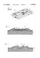
- FIG. 1schematically shows an exemplary prior art TFT
- FIGS. 2 and 3schematically depict exemplary TFTs according to the invention
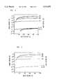
- FIGS. 4 and 5show data on drain current vs. drain voltage for 2 TFTs according to the invention, of somewhat different conductivities;
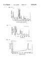
- FIGS. 6 and 7show the X-ray diffraction pattern of, respectively, ⁇ -6T according to the invention, and an exemplary prior art ⁇ -6T;
- FIG. 8shows exemplary differential scanning calorimetry data for ⁇ -6T according to the invention.
- FIG. 9shows an exemplary drive circuit in an active matrix liquid crystal display that comprises TFTs according to the invention.
- FIG. 1schematically depicts a prior art organic TFT 10 of the metal-insulator-semiconductor field effect transistor (MIS-FET) type, wherein numerals 11-16 refer, respectively, to substrate, first electrode (e.g., source electrode), second electrode (e.g., drain electrode), third electrode (gate electrode), insulator layer, and active layer.
- first electrodee.g., source electrode
- second electrodee.g., drain electrode
- gate electrodee.g., third electrode
- FIG. 2schematically shows a MIS-FET type device according to the invention.
- the transistor 20also comprises substrate 11 (e.g., a glass, silicon or plastic body), first and second contacts 12 and 13, third contact 14, gate dielectric 15 and active layer 16.
- substrate 11e.g., a glass, silicon or plastic body
- first and second contacts 12 and 13third contact 14, gate dielectric 15 and active layer 16.
- active layer 16e.g., a glass, silicon or plastic body
- the formercomprises an active layer material that differs significantly from prior art materials, resulting in substantially improved performance (e.g., substantially higher on/off ratio of the source/drain current), as compared to prior art organic TFFs.
- FIG. 3schematically depicts another embodiment of the invention, namely, an organic TFT of the metal-semiconductor (MES)-FET type.
- Numerals 31-35designate, respectively, substrate, active layer, first, second and third contacts.
- MIS-FET type TFTswith 12 ⁇ m channel length and 250 ⁇ m gate length, were fabricated on thermally oxidized, conductive Si substrates.
- the oxide, serving as gate dielectric,was 300 nm thick.
- the gate regionwas accessed by a gold ohmic contact to the Si, and gold source and drain contacts were lithographically defined on the silicon oxide.
- the organic active layerwas then formed by evaporation onto the entire assembly at room temperature and at a pressure of 10 -6 torr.
- the active layerwas 50 nm thick, and was not heat treated. Measurements were made in situ, in vacuum.
- FIG. 4shows curves of drain current vs. drain voltage obtained from an exemplary TFT as described above, with the active layer material ( ⁇ -6T) prepared as described in detail below.
- the off-current (gate voltage 0 or positive, drain voltage -100 V)was about 10 -11 A, and the on/off ratio was greater than 10 6 .
- the as deposited ⁇ -6T at 20° C.had a conductivity below 10 -8 S/cm, (approximately 10 -9 S/cm), and was barely p-type (i.e., it was substantially intrinsic), as those skilled in the art will recognize from the substantial overlap of the curves for 0-60 V gate voltage.
- FIG. 5shows analogous results for a TFT as described above, but with ⁇ -6T of somewhat higher conductivity (approximately 1.4 ⁇ 10 -8 S/cm) due to adventitious impurity doping.
- the carrier mobilitywas about 1-2 ⁇ 10 -2 cm 2 /V ⁇ s, and the on/off ratio was greater than 10 6 for gate voltages between 20 V and -80 V.
- material preparationis a significant aspect of TFTs according to the invention.
- ⁇ -6Tthat can yield material of very low conductivity, exemplarily ⁇ 5 ⁇ 10 -8 S/cm at 20° C.
- Use of such material in a TFTcan result in very low off-current, a feature that inter alia can result in high on/off ratio and good dynamic response of the TFT.
- the closely related compounds ⁇ -8T and ⁇ -4Tcan be made by substantially the same method.
- Reagent grade ⁇ -terthienylwas dissolved in about three times its weight of toluene and applied to a column of ten times its weight of silica gel packed with hexane in a chromatography column. The ⁇ -terthienyl was eluted from the column with hexane and the eluate was concentrated in vacuum. This purified ⁇ -terthienyl (4.5 g) was placed in a round-bottom flask equipped with a magnetic stir bar, and 400 ml of tetrahydrofuran (THF), freshly distilled from sodium benzophenone ketyl, was added. The flask was capped with a rubber stopper.
- THFtetrahydrofuran
- the resulting suspensionwas added via a cannula to a second stirred flask containing a non-halogenating oxidizing agent, e.g., 6.4 g of reagent grade ferric acetylacetonate, and 150 ml of the THF, cooled to ⁇ -70° C. under nitrogen.
- a non-halogenating oxidizing agente.g., 6.4 g of reagent grade ferric acetylacetonate
- the suspended solidswere collected by vacuum filtration and washed in sequence with 100 ml of ethyl ether, 300 ml of 1% HCl in water, 300 ml of (DI) water, 100 ml of ethanol, and 100 ml of ether, yielding 3.5 g of crude solid product.
- the solidwas further washed with 100 ml each of 0.1% Na 2 CO 3 in water, water, water again, ethanol, methyl ethyl ketone, and toluene, all heated to just below boiling and with vigorous shaking to prevent bumping.
- the undissolved solidswere extracted with an inert solvent with boiling point >120° C., e.g., 800 ml of boiling mesitylene under nitrogen for one hour.
- the extractwas filtered at the boiling point through a funnel heated with the vapors of the same solvent (e.g., mesitylene) that was boiling in the receiving flask.
- the filtratewas allowed to cool to ambient temperature, and crystals were obtained.
- the supernatantwas separated from the crystals by suction filtration and used to further extract the undissolved solids. A total of 1.5 g of crystals were obtained.
- Portions of 200-300 mg of the thus produced crystalswere placed at the bottom of a glass sublimator measuring 5 cm in diameter and 6-12 cm high. The material was sublimed >1 cm along the glass tube by heating at about 300° C. and 10 -4 torr. After cooling under vacuum to ambient temperature, the sublimed material was scraped from the glass tube.
- the above described exemplary novel method of making ⁇ -6Tcomprises features. that can significantly affect product quality. Among these is the use of a non-halogenating oxidizing agent, exemplarily ferric acetylacetonate.
- a non-halogenating oxidizing agentexemplarily ferric acetylacetonate.
- prior art ⁇ -6Te.g., ⁇ -6T made with cupric chloride
- the ⁇ -6T made according to the above described methodthus typically differs significantly from prior art ⁇ -6T with regard to elemental analysis.
- Preferred methods of making ⁇ -6Talso comprise solid extraction with an inert solvent with boiling point greater than 120° C., exemplarily mesitylene, and isolation of the ⁇ -6T by crystallization of the extract.
- the preferred methodsfurther comprise a multi-step washing sequence applied to the (pre-washed) crude solid product, and sublimation of the washed solid product along a significant distance, typically >1 cm.
- ⁇ -6T made according to the above described methodhas a melting point that differs substantially from reported melting points of prior art ⁇ -6T, which are in the range 280°-307° C. Specifically, using differential scanning calorimetry under nitrogen, we found the melting point of the novel ⁇ -6T to be about 313° C., as demonstrated by FIG. 8.
- material according to the inventionhas more numerous and sharper X-ray peaks.
- ⁇ -6T according to the inventionthe prior art peaks (see the above cited article by B. Servet et al.) at about 20° and 22.5° each are resolved into at least two peaks.
- ⁇ -6T according to the inventionis a material that can give rise to evaporated films that can exist in a more stable, more dense and better ordered crystalline form than prior art ⁇ -6T.
- electron microscopyhas confirmed that as-deposited films of ⁇ -6T according to the invention (deposited on a substrate at room temperature) can consist of large, anisotropic platelets with lengths of 100-200 nm that are clearly interconnected. This is to be contrasted with similarly deposited prior art ⁇ -6T films which are reported to have grain sizes of 50 nm, with the isotropic grains more or less separated from each other (B. Servet et al., Chemistry of Materials, Vol. 6, (1994), p. 1809).
- the ⁇ -6T films according to the inventioncan have mobility of about 10 -2 cm 2 /V ⁇ s, whereas the above described prior art material was reported to have mobility of only 2 ⁇ 10 -3 cm 2 /V ⁇ s.
- halogen content below 0.1 weight %is an important aspect of active layer material according to the invention, since active layer material with higher halogen content is likely to have relatively low carrier mobility.
- ⁇ -6Tis exemplary, and that modifications of the method are possible.
- alternative inert solventse.g., xylene
- other metal-alkyl reagentse.g., sec-butyllithium
- other non-halogenating oxidizing agentse.g., ferric trifluoro-acetylacetonate, manganese (III) acetylacetonate
- ferric trifluoro-acetylacetonatee.g., ferric trifluoro-acetylacetonate, manganese (III) acetylacetonate
- the methodis not limited to the synthesis of ⁇ -6T but applies, with obvious modifications (e.g., starting material, quantities and temperatures of solvents, sublimation temperature and pressure), also to the preparation of ⁇ -4T and ⁇ -8T, and to the preparation of closely related compounds such as the end-substituted derivatives of ⁇ -6T, ⁇ -4T and ⁇ -8T.
- at least the purification aspects of the novel methodare expected to be applicable, with obvious modifications (e.g., use of solvents of appropriate polarity and boiling point, sublimation temperature and pressure) to other related compounds such as ⁇ -5T, ⁇ -7T and ⁇ -9T, and their 4 or 5 substituted derivatives.
- ⁇ -6Tproduced as described above was placed into a conventional tungsten boat in a conventional evaporator system.
- the base pressure in the evaporation chamberwas about 10 -7 torr.
- the boatwas heated to about 300° C., and a 50 nm thick ⁇ -6T film was deposited uniformly over an appropriate substrate at room temperature.
- the as-deposited materialtypically was polycrystalline, with average grain size of order 100 nm.
- RTArapid thermal annealing
- Annealing an as-deposited ⁇ -6T film for a short timetypically less than 10 seconds, e.g., 1 second
- a temperature close to (optionally even slightly above) the melting pointexemplarily has resulted in increase of the average grain size to above 2 ⁇ m, e.g., in the range 5-100 ⁇ m.
- Annealingis desirably done in an inert atmosphere, e.g., N 2 .
- Any suitable heat sourcee.g., a bank of halogen lamps focused to a susceptor, or a graphite strip heater
- the morphology of the other ⁇ -nTscan also be improved by appropriate RTA.
- RTA of as-deposited p-type ⁇ -6T filmscan result in substantial decrease of the conductivity, with consequent increase in on/off ratio.
- a as-deposited ⁇ -6T layerexhibited a conductivity of about 10 -6 S/cm.
- the layerexhibited a conductivity of 0.7 ⁇ 10 -8 S/cm. It is expected that other members of the group ⁇ -nT will show similar conductivity decreases.
- TFFs according to the inventioncan be produced in substantially the same way as analogous prior an TFTs, provided that a ⁇ -nT of the required low conductivity is used.
- Exemplary substratesare glass, plastics such as MYLAR® or KAPTON®, or Si (coated with SiO 2 or other insulator). Use of encapsulant that protects the active layer material is contemplated.
- Transistors according to the inventioncan be used as discrete devices but will more typically be used in integrated circuits that comprise a multiplicity of transistors according to the invention, possibly in conjunction with conventional semiconductor devices, with conductors interconnecting the devices and providing means for energizing the devices, providing input signals to the circuit and optionally receiving output signals therefrom.
- transistors according to the inventionare used as current switches in liquid crystal displays in functionally the same way as prior art semiconductor TFTs are currently used.
- FIG. 9depicts relevant aspects of an exemplary circuit diagram of an active-matrix liquid crystal display, wherein transistors 101 are TFTs according to the invention, and the remainder of the circuit is conventional.
- Numerals 102refer to liquid crystal
- numerals 103-105refer to signal lines, gate lines and common electrode, respectively.
- Video signals and gate pulsesare also shown schematically.
Landscapes
- Engineering & Computer Science (AREA)
- Chemical & Material Sciences (AREA)
- Physics & Mathematics (AREA)
- Nanotechnology (AREA)
- Materials Engineering (AREA)
- Mathematical Physics (AREA)
- Theoretical Computer Science (AREA)
- Crystallography & Structural Chemistry (AREA)
- Spectroscopy & Molecular Physics (AREA)
- Thin Film Transistor (AREA)
- Electroluminescent Light Sources (AREA)
- Heterocyclic Carbon Compounds Containing A Hetero Ring Having Oxygen Or Sulfur (AREA)
Abstract
Description
Claims (7)
Priority Applications (9)
| Application Number | Priority Date | Filing Date | Title |
|---|---|---|---|
| US08/353,032US5574291A (en) | 1994-12-09 | 1994-12-09 | Article comprising a thin film transistor with low conductivity organic layer |
| TW084101308ATW279260B (en) | 1994-12-09 | 1995-02-14 | |
| CA002160394ACA2160394C (en) | 1994-12-09 | 1995-10-12 | Method of making an organic thin film transistor, and article made by the method |
| EP95308517AEP0716458B1 (en) | 1994-12-09 | 1995-11-28 | Method of making an organic thin film transistor, and article made by the method |
| DE69532794TDE69532794T2 (en) | 1994-12-09 | 1995-11-28 | Process for the preparation of an organic thin film transistor and article produced by this process |
| MX9505068AMX9505068A (en) | 1994-12-09 | 1995-12-05 | Method of making an organic thin film transistor and article made by the method. |
| SG1995002064ASG33623A1 (en) | 1994-12-09 | 1995-12-07 | Method of making an organic thin film transistor and article made by the method |
| KR1019950049121AKR100351009B1 (en) | 1994-12-09 | 1995-12-09 | Apparatus Including Thin Film Transistor and Manufacturing Method of Thin Film Transistor |
| JP34545495AJP3145294B2 (en) | 1994-12-09 | 1995-12-11 | Article comprising thin film transistor and method of manufacturing the same |
Applications Claiming Priority (1)
| Application Number | Priority Date | Filing Date | Title |
|---|---|---|---|
| US08/353,032US5574291A (en) | 1994-12-09 | 1994-12-09 | Article comprising a thin film transistor with low conductivity organic layer |
Publications (1)
| Publication Number | Publication Date |
|---|---|
| US5574291Atrue US5574291A (en) | 1996-11-12 |
Family
ID=23387469
Family Applications (1)
| Application Number | Title | Priority Date | Filing Date |
|---|---|---|---|
| US08/353,032Expired - LifetimeUS5574291A (en) | 1994-12-09 | 1994-12-09 | Article comprising a thin film transistor with low conductivity organic layer |
Country Status (8)
| Country | Link |
|---|---|
| US (1) | US5574291A (en) |
| EP (1) | EP0716458B1 (en) |
| JP (1) | JP3145294B2 (en) |
| KR (1) | KR100351009B1 (en) |
| CA (1) | CA2160394C (en) |
| DE (1) | DE69532794T2 (en) |
| MX (1) | MX9505068A (en) |
| TW (1) | TW279260B (en) |
Cited By (101)
| Publication number | Priority date | Publication date | Assignee | Title |
|---|---|---|---|---|
| US5796121A (en)* | 1997-03-25 | 1998-08-18 | International Business Machines Corporation | Thin film transistors fabricated on plastic substrates |
| US5936259A (en)* | 1997-10-16 | 1999-08-10 | Lucent Technologies Inc. | Thin film transistor and organic semiconductor material thereof |
| US5966594A (en)* | 1993-07-27 | 1999-10-12 | Semiconductor Energy Laboratory Co., Ltd. | Semiconductor device and method for manufacturing the same |
| US6107117A (en)* | 1996-12-20 | 2000-08-22 | Lucent Technologies Inc. | Method of making an organic thin film transistor |
| US6215130B1 (en)* | 1998-08-20 | 2001-04-10 | Lucent Technologies Inc. | Thin film transistors |
| US6278127B1 (en)* | 1994-12-09 | 2001-08-21 | Agere Systems Guardian Corp. | Article comprising an organic thin film transistor adapted for biasing to form a N-type or a P-type transistor |
| US6312971B1 (en) | 1999-08-31 | 2001-11-06 | E Ink Corporation | Solvent annealing process for forming a thin semiconductor film with advantageous properties |
| DE10045192A1 (en)* | 2000-09-13 | 2002-04-04 | Siemens Ag | Organic data storage, RFID tag with organic data storage, use of an organic data storage |
| US6384804B1 (en) | 1998-11-25 | 2002-05-07 | Lucent Techonologies Inc. | Display comprising organic smart pixels |
| US20020170090A1 (en)* | 1997-02-18 | 2002-11-14 | Washington State University Research Foundation | Omega-3 fatty acid desaturase |
| US6498114B1 (en) | 1999-04-09 | 2002-12-24 | E Ink Corporation | Method for forming a patterned semiconductor film |
| US6518949B2 (en)* | 1998-04-10 | 2003-02-11 | E Ink Corporation | Electronic displays using organic-based field effect transistors |
| US6545291B1 (en) | 1999-08-31 | 2003-04-08 | E Ink Corporation | Transistor design for use in the construction of an electronically driven display |
| US20030080426A1 (en)* | 2001-10-30 | 2003-05-01 | Hagen Klauk | Method and device for reducing the contact resistance in organic field-effect transistors by embedding nanoparticles to produce field boosting |
| US20030107265A1 (en)* | 2000-07-18 | 2003-06-12 | Armin Arnold | Method and brake system for controlling the braking process in a motor vehicle |
| US6593690B1 (en) | 1999-09-03 | 2003-07-15 | 3M Innovative Properties Company | Large area organic electronic devices having conducting polymer buffer layers and methods of making same |
| US6611096B1 (en) | 1999-09-03 | 2003-08-26 | 3M Innovative Properties Company | Organic electronic devices having conducting self-doped polymer buffer layers |
| US20030178620A1 (en)* | 2000-09-11 | 2003-09-25 | Adolf Bernds | Organic rectifier, circuit, rfid tag and use of an organic rectifier |
| US20030183817A1 (en)* | 2000-09-01 | 2003-10-02 | Adolf Bernds | Organic field effect transistor, method for structuring an ofet and integrated circuit |
| US20040016886A1 (en)* | 2002-07-25 | 2004-01-29 | General Electric Company | Flexible imager and digital imaging method |
| US20040023447A1 (en)* | 2002-08-02 | 2004-02-05 | Semiconductor Energy Laboratory Co., Ltd. | Organic thin film transistor and method of manufacturing the same, and semiconductor device having the organic thin film transistor |
| US20040029310A1 (en)* | 2000-08-18 | 2004-02-12 | Adoft Bernds | Organic field-effect transistor (ofet), a production method therefor, an integrated circut constructed from the same and their uses |
| US20040026689A1 (en)* | 2000-08-18 | 2004-02-12 | Adolf Bernds | Encapsulated organic-electronic component, method for producing the same and use thereof |
| US20040026121A1 (en)* | 2000-09-22 | 2004-02-12 | Adolf Bernds | Electrode and/or conductor track for organic components and production method thereof |
| US6704133B2 (en) | 1998-03-18 | 2004-03-09 | E-Ink Corporation | Electro-optic display overlays and systems for addressing such displays |
| US20040063267A1 (en)* | 2000-12-08 | 2004-04-01 | Adolf Bernds | Organic field-effect transistor, method for structuring and ofet and integrated circuit |
| US20040062294A1 (en)* | 2000-12-08 | 2004-04-01 | Wolfgang Clemens | Device for detecting and/or transmitting at least one environmental influence, method for producing said device and use thereof |
| US20040075093A1 (en)* | 2001-06-01 | 2004-04-22 | Semiconductor Energy Laboratory Co., Ltd. | Organic semiconductor device and process of manufacturing the same |
| US20040092690A1 (en)* | 2000-12-20 | 2004-05-13 | Mark Giles | Organic semiconductor, production method therefor and the use thereof |
| US6736985B1 (en)* | 1999-05-05 | 2004-05-18 | Agere Systems Inc. | High-resolution method for patterning a substrate with micro-printing |
| US20040094771A1 (en)* | 2001-03-26 | 2004-05-20 | Adolf Bernds | Device with at least two organic electronic components and method for producing the same |
| US6784017B2 (en) | 2002-08-12 | 2004-08-31 | Precision Dynamics Corporation | Method of creating a high performance organic semiconductor device |
| US20040256467A1 (en)* | 2001-10-18 | 2004-12-23 | Wolfgang Clemens | Electronic unit, circuit design for the same, and production method |
| US20040262599A1 (en)* | 2001-06-01 | 2004-12-30 | Adolf Bernds | Organic field effect transistor, method for production and use thereof in the assembly of integrated circuits |
| US6839158B2 (en) | 1997-08-28 | 2005-01-04 | E Ink Corporation | Encapsulated electrophoretic displays having a monolayer of capsules and materials and methods for making the same |
| US6842657B1 (en) | 1999-04-09 | 2005-01-11 | E Ink Corporation | Reactive formation of dielectric layers and protection of organic layers in organic semiconductor device fabrication |
| US20050048803A1 (en)* | 2001-10-16 | 2005-03-03 | Erwann Guillet | Insulator for an organic electronic component |
| US20050045885A1 (en)* | 2003-08-28 | 2005-03-03 | Kim Bo Sung | Thin film transistor array panel using organic semiconductor and a method for manufacturing the same |
| US6864875B2 (en) | 1998-04-10 | 2005-03-08 | E Ink Corporation | Full color reflective display with multichromatic sub-pixels |
| US20050106507A1 (en)* | 2002-03-21 | 2005-05-19 | Adolf Bernds | Device and method for laser structuring functional polymers and the use thereof |
| US20050121728A1 (en)* | 2003-12-04 | 2005-06-09 | Lucent Technologies Inc. | OFETs with active channels formed of densified layers |
| US20050142496A1 (en)* | 2003-12-24 | 2005-06-30 | Kang Seung Y. | Method of fabricating bottom gate type organic thin film transistor |
| US20050140840A1 (en)* | 2003-12-26 | 2005-06-30 | Semiconductor Energy Laboratory Co., Ltd. | Method for manufacturing an organic semiconductor element |
| US20050139823A1 (en)* | 2003-12-26 | 2005-06-30 | Semiconductor Energy Laboratory Co. Ltd. | Organic semiconductor device and method for manufacturing the same |
| US20050173701A1 (en)* | 2004-02-09 | 2005-08-11 | Seiko Epson Corporation | Transistor, circuit board, display and electronic equipment |
| US20050189876A1 (en)* | 2002-03-14 | 2005-09-01 | Semiconductor Energy Laboratory Co., Ltd. | Display device and method of fabricating the same |
| US20050211972A1 (en)* | 2001-12-11 | 2005-09-29 | Siemens Aktiengesellschaft | Organic field effect transistor with off-set threshold voltage and the use thereof |
| US20050211973A1 (en)* | 2004-03-23 | 2005-09-29 | Kiyotaka Mori | Stressed organic semiconductor |
| US20050224787A1 (en)* | 2002-06-13 | 2005-10-13 | Wolfgang Clemens | Substrate for an organic field effect transistor, use of said substrate, method for increasing the charge carrier mobility, and organic field effect transistor (ofet) |
| US20050247928A1 (en)* | 2002-06-20 | 2005-11-10 | Canon Kabushiki Kaisha | Organic semiconductor element, production mehtod therefor and organic semiconductor device |
| US20050275056A1 (en)* | 2004-05-26 | 2005-12-15 | Stephen Forrest | Organic heterojunction bipolar transistor |
| US20050277240A1 (en)* | 2002-03-21 | 2005-12-15 | Walter Fix | Logic components from organic field effect transistors |
| US20060035423A1 (en)* | 2002-11-19 | 2006-02-16 | Walter Fix | Organic electronic component comprising the same organic material for at least two functional layers |
| US20060057769A1 (en)* | 2003-01-21 | 2006-03-16 | Adolf Bernds | Use of conductive carbon black/graphite mixtures for the production of low-cost electronics |
| US20060079327A1 (en)* | 2002-08-08 | 2006-04-13 | Wolfgang Clemens | Electronic device |
| US20060091460A1 (en)* | 2004-10-28 | 2006-05-04 | Gregory Herman | Semiconductor devices and methods of making |
| US20060118778A1 (en)* | 2002-11-05 | 2006-06-08 | Wolfgang Clemens | Organic electronic component with high-resolution structuring and method for the production thereof |
| US20060118780A1 (en)* | 2003-01-09 | 2006-06-08 | Axel Gerlt | Organo-resistive memory unit |
| US20060118779A1 (en)* | 2002-11-19 | 2006-06-08 | Wolfgang Clemens | Organic Electronic Component Comprising A Patterned, Semi-Conducting Functional Layer And A Method For Producing Said Component |
| US20060138701A1 (en)* | 2003-07-03 | 2006-06-29 | Jurgen Ficker | Method and device for structuring organic layers |
| US20060160266A1 (en)* | 2003-01-21 | 2006-07-20 | Adolf Bernds | Organic electronic component and method for producing organic electronic devices |
| US20060214571A1 (en)* | 2005-03-25 | 2006-09-28 | Semiconductor Energy Laboratory Co., Ltd. | Organic semiconductor device |
| US20060220126A1 (en)* | 2003-03-07 | 2006-10-05 | Bart-Hendrik Huisman | Method of manufacturing an electronic arrangement |
| US20060220005A1 (en)* | 2003-07-03 | 2006-10-05 | Walter Fix | Logic gate with a potential-free gate electrode for organic integrated circuits |
| US20070008019A1 (en)* | 2003-09-03 | 2007-01-11 | Wolfgang Clemens | Mechanical control elements for organic polymer electronic devices |
| US7167155B1 (en) | 1995-07-20 | 2007-01-23 | E Ink Corporation | Color electrophoretic displays |
| US20070017401A1 (en)* | 2003-09-03 | 2007-01-25 | Polyic Gmbh & Co. Kg | Polymer mixtures for printed polymer electronic circuits |
| US20070030623A1 (en)* | 2003-08-20 | 2007-02-08 | Polyic Gmbh & Co. Kg | Organic capacitor having a voltage-controlled capacitance |
| US20070051940A1 (en)* | 2003-01-29 | 2007-03-08 | Wolfgang Clemens | Device and method for determining the physical condition of an animal |
| US7238961B2 (en) | 2001-02-09 | 2007-07-03 | Polyic Gmbh & Co. Kg | Organic field effect transistor with a photostructured gate dielectric, method for the production and use thereof in organic electronics |
| US7242513B2 (en) | 1997-08-28 | 2007-07-10 | E Ink Corporation | Encapsulated electrophoretic displays having a monolayer of capsules and materials and methods for making the same |
| US20070215863A1 (en)* | 2006-03-15 | 2007-09-20 | Lucent Technologies Inc. | Fabricating apparatus with doped organic semiconductors |
| US20080061986A1 (en)* | 2004-08-23 | 2008-03-13 | Polylc Gmbh & Co. Kg | External Package Capable of Being Radio-Tagged |
| US7414513B2 (en) | 2002-08-23 | 2008-08-19 | Polyic Gmbh & Co. Kg | Organic component for overvoltage protection and associated circuit |
| US20080197343A1 (en)* | 2004-12-10 | 2008-08-21 | Robert Blache | Organic Field Effect Transistor Gate |
| US20080204069A1 (en)* | 2005-03-01 | 2008-08-28 | Polyic Gmbh & Co. Kg | Electronic Module With Organic Logic Circuit Elements |
| US20080218315A1 (en)* | 2004-12-10 | 2008-09-11 | Markus Bohm | Electronic Component Comprising a Modulator |
| US7479670B2 (en) | 2003-08-25 | 2009-01-20 | Polyic Gmbh & Co Kg | Organic electronic component with high resolution structuring, and method of the production thereof |
| US20090121218A1 (en)* | 2006-03-22 | 2009-05-14 | Polyic Gmbh & Co. Kg | Method for programming an electronic circuit and electronic circuit |
| US20090189147A1 (en)* | 2004-01-14 | 2009-07-30 | Walter Fix | Organic transistor comprising a self-aligning gate electrode, and method for the production thereof |
| EP2085401A1 (en) | 2008-01-22 | 2009-08-05 | Ricoh Company, Ltd. | Benzobisthiazole compound, benzobisthiazole polymer, organic film including the compound or polymer and transistor including the organic film |
| US20090237248A1 (en)* | 2004-12-10 | 2009-09-24 | Wolfgang Clemens | Identification System |
| US7641857B2 (en) | 2002-11-14 | 2010-01-05 | Polyic Gmbh & Co. Kg | Measuring apparatus used for determining an analyte in a liquid sample, comprising polymer electronic components |
| US20100019234A1 (en)* | 2006-12-04 | 2010-01-28 | Masatoshi Saito | Organic thin film transistor and organic thin film light emitting transistor |
| US20100025670A1 (en)* | 2006-12-04 | 2010-02-04 | Idemitsu Kosan Co., Ltd. | Organic Thin Film Transistor and Organic Thin Film Light Emitting Transistor |
| US7724550B2 (en) | 2004-12-23 | 2010-05-25 | Polyic Gmbh & Co. Kg | Organic rectifier |
| US20100237332A1 (en)* | 2009-03-23 | 2010-09-23 | Fuji Xerox Co., Ltd. | Organic semiconductor transistor |
| US20100243995A1 (en)* | 2009-03-24 | 2010-09-30 | Fuji Xerox Co., Ltd. | Organic semiconductor transistor, method of producing the same, and electronic device |
| US7812343B2 (en) | 2005-04-15 | 2010-10-12 | Polyic Gmbh & Co. Kg | Multilayer composite body having an electronic function |
| US7821000B2 (en) | 2008-02-01 | 2010-10-26 | Alcatel-Lucent Usa Inc. | Method of doping organic semiconductors |
| US20100276672A1 (en)* | 2009-04-30 | 2010-11-04 | Fuji Xerox Co., Ltd. | Organic electroluminescent device and display medium |
| US7843342B2 (en) | 2005-03-01 | 2010-11-30 | Polyic Gmbh & Co. Kg | Organic clock generator |
| US7846838B2 (en) | 2005-07-29 | 2010-12-07 | Polyic Gmbh & Co. Kg | Method for producing an electronic component |
| US7940340B2 (en) | 2005-07-04 | 2011-05-10 | Polyic Gmbh & Co. Kg | Multilayer body with electrically controllable optically active systems of layers |
| US8044517B2 (en) | 2002-07-29 | 2011-10-25 | Polyic Gmbh & Co. Kg | Electronic component comprising predominantly organic functional materials and a method for the production thereof |
| JP2011258891A (en)* | 2010-06-11 | 2011-12-22 | Fuji Xerox Co Ltd | Organic transistor and method of manufacturing organic transistor |
| US8315061B2 (en) | 2005-09-16 | 2012-11-20 | Polyic Gmbh & Co. Kg | Electronic circuit with elongated strip layer and method for the manufacture of the same |
| US8470617B2 (en) | 2006-04-07 | 2013-06-25 | Qd Vision, Inc. | Composition including material, methods of depositing material, articles including same and systems for depositing material |
| US8716703B2 (en) | 2011-12-26 | 2014-05-06 | Fuji Xerox Co., Ltd. | Organic semiconductor transistor |
| US9011729B2 (en) | 2010-04-22 | 2015-04-21 | Idemitsu Kosan Co., Ltd. | Organic thin-film transistor |
| US9120149B2 (en) | 2006-06-24 | 2015-09-01 | Qd Vision, Inc. | Methods and articles including nanomaterial |
Families Citing this family (20)
| Publication number | Priority date | Publication date | Assignee | Title |
|---|---|---|---|---|
| EP1438757A2 (en)* | 2001-10-01 | 2004-07-21 | Koninklijke Philips Electronics N.V. | Composition, method and electronic device |
| JP3856202B2 (en) | 2001-10-05 | 2006-12-13 | 日本電気株式会社 | Organic thin film transistor |
| JP3823312B2 (en) | 2001-10-18 | 2006-09-20 | 日本電気株式会社 | Organic thin film transistor |
| US20060243965A1 (en)* | 2003-01-28 | 2006-11-02 | De Leeuw Dagobert M | Electronic device |
| US7166689B2 (en) | 2003-02-13 | 2007-01-23 | Ricoh Company, Ltd. | Aryl amine polymer, thin film transistor using the aryl amine polymer, and method of manufacturing the thin film transistor |
| US7297621B2 (en) | 2003-04-15 | 2007-11-20 | California Institute Of Technology | Flexible carbon-based ohmic contacts for organic transistors |
| CN100428521C (en) | 2003-11-17 | 2008-10-22 | 富士施乐株式会社 | Organic Semiconductor Transistor Elements |
| JP4877869B2 (en)* | 2003-12-26 | 2012-02-15 | 株式会社半導体エネルギー研究所 | Method for producing organic semiconductor element |
| JP2005268550A (en)* | 2004-03-18 | 2005-09-29 | Japan Science & Technology Agency | Organic semiconductor, semiconductor device using the same, and manufacturing method thereof |
| JP4449549B2 (en) | 2004-04-15 | 2010-04-14 | 日本電気株式会社 | ORGANIC THIN FILM TRANSISTOR USING MATERIAL HAVING BRIDGED CYCLIC HYDROCARBON LACTONE STRUCTURE AND MANUFACTURING METHOD |
| KR101133767B1 (en) | 2005-03-09 | 2012-04-09 | 삼성전자주식회사 | Organic thin film transistor array panel and method for manufacturing the same |
| JP4632034B2 (en)* | 2005-03-10 | 2011-02-16 | セイコーエプソン株式会社 | Manufacturing method of organic ferroelectric memory |
| US7521710B2 (en) | 2006-02-16 | 2009-04-21 | Idemitsu Kosan Co., Ltd. | Organic thin film transistor |
| JP2007287961A (en)* | 2006-04-18 | 2007-11-01 | Konica Minolta Holdings Inc | Organic thin film transistor and manufacturing method thereof |
| JP5368797B2 (en) | 2006-10-12 | 2013-12-18 | 出光興産株式会社 | Organic thin film transistor device and organic thin film light emitting transistor |
| US8022401B2 (en) | 2006-11-14 | 2011-09-20 | Idemitsu Kosan, Co., Ltd. | Organic thin film transistor and organic thin film light-emitting transistor |
| EP2083457A4 (en) | 2006-11-14 | 2012-04-25 | Idemitsu Kosan Co | ORGANIC FILM THIN TRANSISTOR AND ORGANIC FILM THIN ELECTROLUMIZING TRANSISTOR |
| US8203139B2 (en) | 2006-11-24 | 2012-06-19 | Idemitsu Kosan Co., Ltd | Organic thin film transistor and organic thin film light-emitting transistor using an organic semiconductor layer having an aromatic hydrocarbon group or an aromatic heterocyclic group in the center thereof |
| JP5308162B2 (en) | 2006-11-24 | 2013-10-09 | 出光興産株式会社 | Organic thin film transistor and organic thin film light emitting transistor |
| KR101582991B1 (en)* | 2014-05-23 | 2016-01-20 | 연세대학교 산학협력단 | Flexible organic thin-film transistor and sensor having the same |
Citations (4)
| Publication number | Priority date | Publication date | Assignee | Title |
|---|---|---|---|---|
| JPH03236286A (en)* | 1990-02-14 | 1991-10-22 | Toshiba Corp | Organic film element |
| US5247190A (en)* | 1989-04-20 | 1993-09-21 | Cambridge Research And Innovation Limited | Electroluminescent devices |
| US5315129A (en)* | 1990-08-20 | 1994-05-24 | University Of Southern California | Organic optoelectronic devices and methods |
| US5355235A (en)* | 1991-08-15 | 1994-10-11 | Kabushiki Kaisha Toshiba | Organic field effect element having organic layers with different carrier concentrations |
- 1994
- 1994-12-09USUS08/353,032patent/US5574291A/ennot_activeExpired - Lifetime
- 1995
- 1995-02-14TWTW084101308Apatent/TW279260B/zhnot_activeIP Right Cessation
- 1995-10-12CACA002160394Apatent/CA2160394C/ennot_activeExpired - Lifetime
- 1995-11-28DEDE69532794Tpatent/DE69532794T2/ennot_activeExpired - Lifetime
- 1995-11-28EPEP95308517Apatent/EP0716458B1/ennot_activeExpired - Lifetime
- 1995-12-05MXMX9505068Apatent/MX9505068A/ennot_activeIP Right Cessation
- 1995-12-09KRKR1019950049121Apatent/KR100351009B1/ennot_activeExpired - Lifetime
- 1995-12-11JPJP34545495Apatent/JP3145294B2/ennot_activeExpired - Fee Related
Patent Citations (4)
| Publication number | Priority date | Publication date | Assignee | Title |
|---|---|---|---|---|
| US5247190A (en)* | 1989-04-20 | 1993-09-21 | Cambridge Research And Innovation Limited | Electroluminescent devices |
| JPH03236286A (en)* | 1990-02-14 | 1991-10-22 | Toshiba Corp | Organic film element |
| US5315129A (en)* | 1990-08-20 | 1994-05-24 | University Of Southern California | Organic optoelectronic devices and methods |
| US5355235A (en)* | 1991-08-15 | 1994-10-11 | Kabushiki Kaisha Toshiba | Organic field effect element having organic layers with different carrier concentrations |
Non-Patent Citations (19)
| Title |
|---|
| "All-Polymer Field-Effect Transistor Realized by Printing Techniques", by F. Garnier et al., Science, vol. 265, 16 Sep. 1994, pp. 1684-1686. |
| "Amorphous and Microcrystalline Devices", J. Kanicki, editor, Artech House, Boston (1991) pp. 102-103. no month. |
| "An Analytical Model for Organic-Based Thin-Film Transistors", by G. Horowitz et al., J. Appl. Phys., vol. 70(1), 1 Jul. 1991, pp. 469-475. |
| "Junction Field-Effect Transistor Using Polythiophene as an Active Component", by S. Miyauchi et al., Synthetic Metals., vol. 41-43 (1991), pp. 1155-1158. no month. |
| "Polymorphism and Charge Transport in Vacuum-Evaporated Sexithiophene Films", by B. Servet et al., Chemistry of Materials, vol. 6, (1994), p. 1809. no month. |
| "Polythienylenevinylene Thin-Film Transistor with High Carrier Mobility", by H. Fuchigami et al., Appl. Phys. Lett., vol. 63(10), 6 Sep. 1993, pp. 1372-1374. |
| "Polythiophene Field-Effect Transistor With Polypyrrole Worked as Source and Drain Electrodes", by H. Koezuka et al., Appl. Phys. Lett., vol. 62(15), 12 Apr. 1993, pp. 1794-1796. |
| "Thin-Film Transistors Based on Alpha-Conjugated Oligomers", by G. Horowitz et al., Synthetic Metals, vol. 41-43 (1991), pp. 1127-1130. no month. |
| "X-Ray Determination of the Crystal Structure and Orientation of Vacuum Evaporated Sexithiophene Films", by B. Servet et al., Advanced Materials, vol. 5, No. 6, p. 461 (1993). no month. |
| All Polymer Field Effect Transistor Realized by Printing Techniques , by F. Garnier et al., Science, vol. 265, 16 Sep. 1994, pp. 1684 1686.* |
| Amorphous and Microcrystalline Devices , J. Kanicki, editor, Artech House, Boston (1991) pp. 102 103. no month.* |
| An Analytical Model for Organic Based Thin Film Transistors , by G. Horowitz et al., J. Appl. Phys., vol. 70(1), 1 Jul. 1991, pp. 469 475.* |
| Chemical Abstracts, vol. 114, p. 22, item 186387g (1991). no month.* |
| Junction Field Effect Transistor Using Polythiophene as an Active Component , by S. Miyauchi et al., Synthetic Metals., vol. 41 43 (1991), pp. 1155 1158. no month.* |
| Polymorphism and Charge Transport in Vacuum Evaporated Sexithiophene Films , by B. Servet et al., Chemistry of Materials, vol. 6, (1994), p. 1809. no month.* |
| Polythienylenevinylene Thin Film Transistor with High Carrier Mobility , by H. Fuchigami et al., Appl. Phys. Lett., vol. 63(10), 6 Sep. 1993, pp. 1372 1374.* |
| Polythiophene Field Effect Transistor With Polypyrrole Worked as Source and Drain Electrodes , by H. Koezuka et al., Appl. Phys. Lett., vol. 62(15), 12 Apr. 1993, pp. 1794 1796.* |
| Thin Film Transistors Based on Alpha Conjugated Oligomers , by G. Horowitz et al., Synthetic Metals, vol. 41 43 (1991), pp. 1127 1130. no month.* |
| X Ray Determination of the Crystal Structure and Orientation of Vacuum Evaporated Sexithiophene Films , by B. Servet et al., Advanced Materials, vol. 5, No. 6, p. 461 (1993). no month.* |
Cited By (181)
| Publication number | Priority date | Publication date | Assignee | Title |
|---|---|---|---|---|
| US5966594A (en)* | 1993-07-27 | 1999-10-12 | Semiconductor Energy Laboratory Co., Ltd. | Semiconductor device and method for manufacturing the same |
| US6210997B1 (en) | 1993-07-27 | 2001-04-03 | Semiconductor Energy Laboratory Co., Ltd. | Semiconductor device and method for manufacturing the same |
| US6465284B2 (en) | 1993-07-27 | 2002-10-15 | Semiconductor Energy Laboratory Co., Ltd. | Semiconductor device and method for manufacturing the same |
| US6278127B1 (en)* | 1994-12-09 | 2001-08-21 | Agere Systems Guardian Corp. | Article comprising an organic thin film transistor adapted for biasing to form a N-type or a P-type transistor |
| US7167155B1 (en) | 1995-07-20 | 2007-01-23 | E Ink Corporation | Color electrophoretic displays |
| US6107117A (en)* | 1996-12-20 | 2000-08-22 | Lucent Technologies Inc. | Method of making an organic thin film transistor |
| US20020170090A1 (en)* | 1997-02-18 | 2002-11-14 | Washington State University Research Foundation | Omega-3 fatty acid desaturase |
| US5796121A (en)* | 1997-03-25 | 1998-08-18 | International Business Machines Corporation | Thin film transistors fabricated on plastic substrates |
| US7242513B2 (en) | 1997-08-28 | 2007-07-10 | E Ink Corporation | Encapsulated electrophoretic displays having a monolayer of capsules and materials and methods for making the same |
| US6839158B2 (en) | 1997-08-28 | 2005-01-04 | E Ink Corporation | Encapsulated electrophoretic displays having a monolayer of capsules and materials and methods for making the same |
| US5936259A (en)* | 1997-10-16 | 1999-08-10 | Lucent Technologies Inc. | Thin film transistor and organic semiconductor material thereof |
| US6704133B2 (en) | 1998-03-18 | 2004-03-09 | E-Ink Corporation | Electro-optic display overlays and systems for addressing such displays |
| US8466852B2 (en) | 1998-04-10 | 2013-06-18 | E Ink Corporation | Full color reflective display with multichromatic sub-pixels |
| US6518949B2 (en)* | 1998-04-10 | 2003-02-11 | E Ink Corporation | Electronic displays using organic-based field effect transistors |
| US7075502B1 (en) | 1998-04-10 | 2006-07-11 | E Ink Corporation | Full color reflective display with multichromatic sub-pixels |
| US6864875B2 (en) | 1998-04-10 | 2005-03-08 | E Ink Corporation | Full color reflective display with multichromatic sub-pixels |
| US6215130B1 (en)* | 1998-08-20 | 2001-04-10 | Lucent Technologies Inc. | Thin film transistors |
| US6384804B1 (en) | 1998-11-25 | 2002-05-07 | Lucent Techonologies Inc. | Display comprising organic smart pixels |
| US6498114B1 (en) | 1999-04-09 | 2002-12-24 | E Ink Corporation | Method for forming a patterned semiconductor film |
| US6842657B1 (en) | 1999-04-09 | 2005-01-11 | E Ink Corporation | Reactive formation of dielectric layers and protection of organic layers in organic semiconductor device fabrication |
| US6736985B1 (en)* | 1999-05-05 | 2004-05-18 | Agere Systems Inc. | High-resolution method for patterning a substrate with micro-printing |
| US6545291B1 (en) | 1999-08-31 | 2003-04-08 | E Ink Corporation | Transistor design for use in the construction of an electronically driven display |
| US20030141500A1 (en)* | 1999-08-31 | 2003-07-31 | E Ink Corporation | Transistor design for use in the construction of an electronically driven display |
| US6750473B2 (en) | 1999-08-31 | 2004-06-15 | E-Ink Corporation | Transistor design for use in the construction of an electronically driven display |
| US6312971B1 (en) | 1999-08-31 | 2001-11-06 | E Ink Corporation | Solvent annealing process for forming a thin semiconductor film with advantageous properties |
| US6611096B1 (en) | 1999-09-03 | 2003-08-26 | 3M Innovative Properties Company | Organic electronic devices having conducting self-doped polymer buffer layers |
| US20030209973A1 (en)* | 1999-09-03 | 2003-11-13 | 3M Innovative Properties Company | Large area organic electronic devices having conducting polymer buffer layers and methods of making same |
| US6593690B1 (en) | 1999-09-03 | 2003-07-15 | 3M Innovative Properties Company | Large area organic electronic devices having conducting polymer buffer layers and methods of making same |
| US20030107265A1 (en)* | 2000-07-18 | 2003-06-12 | Armin Arnold | Method and brake system for controlling the braking process in a motor vehicle |
| US20040026689A1 (en)* | 2000-08-18 | 2004-02-12 | Adolf Bernds | Encapsulated organic-electronic component, method for producing the same and use thereof |
| US7875975B2 (en) | 2000-08-18 | 2011-01-25 | Polyic Gmbh & Co. Kg | Organic integrated circuit completely encapsulated by multi-layered barrier and included in RFID tag |
| US20040029310A1 (en)* | 2000-08-18 | 2004-02-12 | Adoft Bernds | Organic field-effect transistor (ofet), a production method therefor, an integrated circut constructed from the same and their uses |
| US20030183817A1 (en)* | 2000-09-01 | 2003-10-02 | Adolf Bernds | Organic field effect transistor, method for structuring an ofet and integrated circuit |
| US6960489B2 (en) | 2000-09-01 | 2005-11-01 | Siemens Aktiengesellschaft | Method for structuring an OFET |
| US20030178620A1 (en)* | 2000-09-11 | 2003-09-25 | Adolf Bernds | Organic rectifier, circuit, rfid tag and use of an organic rectifier |
| US6903958B2 (en) | 2000-09-13 | 2005-06-07 | Siemens Aktiengesellschaft | Method of writing to an organic memory |
| US20040026690A1 (en)* | 2000-09-13 | 2004-02-12 | Adolf Bernds | Organic memory, identification marker (rfid-tag) with organic memory and uses of an organic memory |
| DE10045192A1 (en)* | 2000-09-13 | 2002-04-04 | Siemens Ag | Organic data storage, RFID tag with organic data storage, use of an organic data storage |
| US20040026121A1 (en)* | 2000-09-22 | 2004-02-12 | Adolf Bernds | Electrode and/or conductor track for organic components and production method thereof |
| US7229868B2 (en) | 2000-12-08 | 2007-06-12 | Polyic Gmbh & Co. Kg | Organic field-effect transistor, method for structuring an OFET and integrated circuit |
| US20040062294A1 (en)* | 2000-12-08 | 2004-04-01 | Wolfgang Clemens | Device for detecting and/or transmitting at least one environmental influence, method for producing said device and use thereof |
| US7534034B2 (en)* | 2000-12-08 | 2009-05-19 | Polyic Gmbh & Co. Kg | Device for detecting at least one environmental influence |
| US20040063267A1 (en)* | 2000-12-08 | 2004-04-01 | Adolf Bernds | Organic field-effect transistor, method for structuring and ofet and integrated circuit |
| US20040092690A1 (en)* | 2000-12-20 | 2004-05-13 | Mark Giles | Organic semiconductor, production method therefor and the use thereof |
| US7238961B2 (en) | 2001-02-09 | 2007-07-03 | Polyic Gmbh & Co. Kg | Organic field effect transistor with a photostructured gate dielectric, method for the production and use thereof in organic electronics |
| US20040094771A1 (en)* | 2001-03-26 | 2004-05-20 | Adolf Bernds | Device with at least two organic electronic components and method for producing the same |
| US20040075093A1 (en)* | 2001-06-01 | 2004-04-22 | Semiconductor Energy Laboratory Co., Ltd. | Organic semiconductor device and process of manufacturing the same |
| US7015502B2 (en) | 2001-06-01 | 2006-03-21 | Semiconductor Energy Laboratory Co., Ltd. | Organic semiconductor device and process of manufacturing the same |
| US7554113B2 (en) | 2001-06-01 | 2009-06-30 | Semiconductor Energy Laboratory Co., Ltd. | Organic semiconductor device |
| US20040262599A1 (en)* | 2001-06-01 | 2004-12-30 | Adolf Bernds | Organic field effect transistor, method for production and use thereof in the assembly of integrated circuits |
| US20060131573A1 (en)* | 2001-06-01 | 2006-06-22 | Semiconductor Energy Laboratory Co., Ltd. | Organic semiconductor device and process of manufacturing the same |
| US7298023B2 (en) | 2001-10-16 | 2007-11-20 | Polyic Gmbh & Co. Kg | Electronic device with organic insulator |
| US20050048803A1 (en)* | 2001-10-16 | 2005-03-03 | Erwann Guillet | Insulator for an organic electronic component |
| US20040256467A1 (en)* | 2001-10-18 | 2004-12-23 | Wolfgang Clemens | Electronic unit, circuit design for the same, and production method |
| US7483275B2 (en) | 2001-10-18 | 2009-01-27 | Polyic Gmbh & Co. Kg | Electronic unit, circuit design for the same, and production method |
| US7067840B2 (en)* | 2001-10-30 | 2006-06-27 | Infineon Technologies Ag | Method and device for reducing the contact resistance in organic field-effect transistors by embedding nanoparticles to produce field boosting |
| US20030080426A1 (en)* | 2001-10-30 | 2003-05-01 | Hagen Klauk | Method and device for reducing the contact resistance in organic field-effect transistors by embedding nanoparticles to produce field boosting |
| US20050211972A1 (en)* | 2001-12-11 | 2005-09-29 | Siemens Aktiengesellschaft | Organic field effect transistor with off-set threshold voltage and the use thereof |
| US7064345B2 (en) | 2001-12-11 | 2006-06-20 | Siemens Aktiengesellschaft | Organic field effect transistor with off-set threshold voltage and the use thereof |
| US20050189876A1 (en)* | 2002-03-14 | 2005-09-01 | Semiconductor Energy Laboratory Co., Ltd. | Display device and method of fabricating the same |
| US7378791B2 (en) | 2002-03-14 | 2008-05-27 | Semiconductor Energy Laboratory Co., Ltd. | Display device comprising contrast medium |
| US20080248609A1 (en)* | 2002-03-14 | 2008-10-09 | Semiconductor Energy Laboratory Co., Ltd. | Display device and method of fabricating the same |
| US10088732B2 (en) | 2002-03-14 | 2018-10-02 | Semiconductor Energy Laboratory Co., Ltd. | Display device and method of fabricating the same |
| US10663834B2 (en) | 2002-03-14 | 2020-05-26 | Semiconductor Energy Laboratory Co., Ltd. | Display device and method of fabricating the same |
| US9513528B2 (en) | 2002-03-14 | 2016-12-06 | Semiconductor Energy Laboratory Co., Ltd. | Display device and method of fabricating the same |
| US9122119B2 (en) | 2002-03-14 | 2015-09-01 | Semiconductor Energy Laboratory Co., Ltd. | Display device and method of fabricating the same |
| US7978399B2 (en) | 2002-03-14 | 2011-07-12 | Semiconductor Energy Laboratory Co., Ltd. | Display device and method of fabricating the same |
| US8599469B2 (en) | 2002-03-14 | 2013-12-03 | Semiconductor Energy Laboratory Co., Ltd. | Display device and method of fabricating the same |
| US7223995B2 (en) | 2002-03-21 | 2007-05-29 | Polyic Gmbh & Co. Kg | Logic components comprising organic field effect transistors |
| US20050277240A1 (en)* | 2002-03-21 | 2005-12-15 | Walter Fix | Logic components from organic field effect transistors |
| US20050106507A1 (en)* | 2002-03-21 | 2005-05-19 | Adolf Bernds | Device and method for laser structuring functional polymers and the use thereof |
| US20050224787A1 (en)* | 2002-06-13 | 2005-10-13 | Wolfgang Clemens | Substrate for an organic field effect transistor, use of said substrate, method for increasing the charge carrier mobility, and organic field effect transistor (ofet) |
| US7709865B2 (en) | 2002-06-13 | 2010-05-04 | Polyic Gmbh & Co. Kg | Substrate for an organic field effect transistor, use of said substrate, method of increasing the charge carrier mobility, and organic field effect transistor (OFET) |
| US7202495B2 (en) | 2002-06-20 | 2007-04-10 | Canon Kabushiki Kaisha | Organic semiconductor element, production method therefor and organic semiconductor device |
| US20050247928A1 (en)* | 2002-06-20 | 2005-11-10 | Canon Kabushiki Kaisha | Organic semiconductor element, production mehtod therefor and organic semiconductor device |
| US20040016886A1 (en)* | 2002-07-25 | 2004-01-29 | General Electric Company | Flexible imager and digital imaging method |
| US7078702B2 (en) | 2002-07-25 | 2006-07-18 | General Electric Company | Imager |
| US8044517B2 (en) | 2002-07-29 | 2011-10-25 | Polyic Gmbh & Co. Kg | Electronic component comprising predominantly organic functional materials and a method for the production thereof |
| US20100038636A1 (en)* | 2002-08-02 | 2010-02-18 | Semiconductor Energy Laboratory Co., Ltd. | Organic thin film transistor and method of manufacturing the same, and semiconductor device having the organic thin film transistor |
| US8368065B2 (en) | 2002-08-02 | 2013-02-05 | Semiconductor Energy Laboratory Co., Ltd. | Organic thin film transistor and method of manufacturing the same, and semiconductor device having the organic thin film transistor |
| US7985967B2 (en) | 2002-08-02 | 2011-07-26 | Semiconductor Energy Laboratory Co., Ltd. | Organic thin film transistor and method of manufacturing the same, and semiconductor device having the organic thin film transistor |
| US20050062065A1 (en)* | 2002-08-02 | 2005-03-24 | Semiconductor Energy Laboratory Co., Ltd. | Organic thin film transistor and method of manufacturing the same, and semiconductor device having the organic thin film transistor |
| US6821811B2 (en) | 2002-08-02 | 2004-11-23 | Semiconductor Energy Laboratory Co., Ltd. | Organic thin film transistor and method of manufacturing the same, and semiconductor device having the organic thin film transistor |
| US7626196B2 (en) | 2002-08-02 | 2009-12-01 | Semiconductor Energy Laboratory Co., Ltd. | Organic thin film transistor and method of manufacturing the same, and semiconductor device having the organic thin film transistor |
| US20040023447A1 (en)* | 2002-08-02 | 2004-02-05 | Semiconductor Energy Laboratory Co., Ltd. | Organic thin film transistor and method of manufacturing the same, and semiconductor device having the organic thin film transistor |
| US20060079327A1 (en)* | 2002-08-08 | 2006-04-13 | Wolfgang Clemens | Electronic device |
| US20050003574A1 (en)* | 2002-08-12 | 2005-01-06 | Yang Yang | Method of creating a high performance organic semiconductor device |
| US6784017B2 (en) | 2002-08-12 | 2004-08-31 | Precision Dynamics Corporation | Method of creating a high performance organic semiconductor device |
| US7414513B2 (en) | 2002-08-23 | 2008-08-19 | Polyic Gmbh & Co. Kg | Organic component for overvoltage protection and associated circuit |
| US20060118778A1 (en)* | 2002-11-05 | 2006-06-08 | Wolfgang Clemens | Organic electronic component with high-resolution structuring and method for the production thereof |
| US7641857B2 (en) | 2002-11-14 | 2010-01-05 | Polyic Gmbh & Co. Kg | Measuring apparatus used for determining an analyte in a liquid sample, comprising polymer electronic components |
| US20060035423A1 (en)* | 2002-11-19 | 2006-02-16 | Walter Fix | Organic electronic component comprising the same organic material for at least two functional layers |
| US20060118779A1 (en)* | 2002-11-19 | 2006-06-08 | Wolfgang Clemens | Organic Electronic Component Comprising A Patterned, Semi-Conducting Functional Layer And A Method For Producing Said Component |
| US7442954B2 (en) | 2002-11-19 | 2008-10-28 | Polyic Gmbh & Co. Kg | Organic electronic component comprising a patterned, semi-conducting functional layer and a method for producing said component |
| US20060118780A1 (en)* | 2003-01-09 | 2006-06-08 | Axel Gerlt | Organo-resistive memory unit |
| US20060057769A1 (en)* | 2003-01-21 | 2006-03-16 | Adolf Bernds | Use of conductive carbon black/graphite mixtures for the production of low-cost electronics |
| US20060160266A1 (en)* | 2003-01-21 | 2006-07-20 | Adolf Bernds | Organic electronic component and method for producing organic electronic devices |
| US7329559B2 (en) | 2003-01-21 | 2008-02-12 | Polyic Gmbh & Co. Kg | Use of conductive carbon black/graphite mixtures for the production of low-cost electronics |
| US20070051940A1 (en)* | 2003-01-29 | 2007-03-08 | Wolfgang Clemens | Device and method for determining the physical condition of an animal |
| US20060220126A1 (en)* | 2003-03-07 | 2006-10-05 | Bart-Hendrik Huisman | Method of manufacturing an electronic arrangement |
| US7820999B2 (en)* | 2003-03-07 | 2010-10-26 | Polymer Vision Limited | Electronic arrangement including a thin film transistor having active and protective layers structured in a same two-dimensional pattern |
| US20060220005A1 (en)* | 2003-07-03 | 2006-10-05 | Walter Fix | Logic gate with a potential-free gate electrode for organic integrated circuits |
| US20060138701A1 (en)* | 2003-07-03 | 2006-06-29 | Jurgen Ficker | Method and device for structuring organic layers |
| US20070030623A1 (en)* | 2003-08-20 | 2007-02-08 | Polyic Gmbh & Co. Kg | Organic capacitor having a voltage-controlled capacitance |
| US7479670B2 (en) | 2003-08-25 | 2009-01-20 | Polyic Gmbh & Co Kg | Organic electronic component with high resolution structuring, and method of the production thereof |
| US20110084260A1 (en)* | 2003-08-28 | 2011-04-14 | Samsung Electronics Co., Ltd | Thin film transistor array panel using organic semiconductor and a method for manufacturing the same |
| US7880170B2 (en)* | 2003-08-28 | 2011-02-01 | Samsung Electronics Co., Ltd. | Thin film transistor array panel using organic semiconductor and a method for manufacturing the same |
| US8319223B2 (en) | 2003-08-28 | 2012-11-27 | Samsung Display Co., Ltd. | Thin film transistor array panel using organic semiconductor and a method for manufacturing the same |
| US20050045885A1 (en)* | 2003-08-28 | 2005-03-03 | Kim Bo Sung | Thin film transistor array panel using organic semiconductor and a method for manufacturing the same |
| US20070008019A1 (en)* | 2003-09-03 | 2007-01-11 | Wolfgang Clemens | Mechanical control elements for organic polymer electronic devices |
| US7678857B2 (en) | 2003-09-03 | 2010-03-16 | Polyic Gmbh & Co. Kg | Polymer mixtures for printed polymer electronic circuits |
| US7576294B2 (en) | 2003-09-03 | 2009-08-18 | Polyic Gmbh & Co. Kg | Mechanical control elements for organic polymer electronic devices |
| US20070017401A1 (en)* | 2003-09-03 | 2007-01-25 | Polyic Gmbh & Co. Kg | Polymer mixtures for printed polymer electronic circuits |
| US7767998B2 (en)* | 2003-12-04 | 2010-08-03 | Alcatel-Lucent Usa Inc. | OFETs with active channels formed of densified layers |
| US20050121728A1 (en)* | 2003-12-04 | 2005-06-09 | Lucent Technologies Inc. | OFETs with active channels formed of densified layers |
| US7459337B2 (en) | 2003-12-24 | 2008-12-02 | Electronics And Telecommunications Research Institute | Method of fabricating bottom gate type organic thin film transistor |
| US20050142496A1 (en)* | 2003-12-24 | 2005-06-30 | Kang Seung Y. | Method of fabricating bottom gate type organic thin film transistor |
| US7749804B2 (en) | 2003-12-26 | 2010-07-06 | Semiconductor Energy Laboratory Co., Ltd. | Organic semiconductor device and method for manufacturing the same |
| US20100151621A1 (en)* | 2003-12-26 | 2010-06-17 | Semiconductor Energy Laboratory Co., Ltd. | Method for manufacturing an organic semiconductor element |
| US7977150B2 (en) | 2003-12-26 | 2011-07-12 | Semiconductor Energy Laboratory Co., Ltd. | Method for manufacturing an organic semiconductor element |
| US7554121B2 (en) | 2003-12-26 | 2009-06-30 | Semiconductor Energy Laboratory Co., Ltd. | Organic semiconductor device |
| US20090209069A1 (en)* | 2003-12-26 | 2009-08-20 | Semiconductor Energy Laboratory Co., Ltd. | Organic semiconductor device and method for manufacturing the same |
| US20110237034A1 (en)* | 2003-12-26 | 2011-09-29 | Semiconductor Energy Laboratory Co., Ltd. | Method for manufacturing an organic semiconductor element |
| US8202760B2 (en) | 2003-12-26 | 2012-06-19 | Semiconductor Energy Laboratory Co., Ltd. | Method for manufacturing an organic semiconductor element |
| US20050139823A1 (en)* | 2003-12-26 | 2005-06-30 | Semiconductor Energy Laboratory Co. Ltd. | Organic semiconductor device and method for manufacturing the same |
| US20050140840A1 (en)* | 2003-12-26 | 2005-06-30 | Semiconductor Energy Laboratory Co., Ltd. | Method for manufacturing an organic semiconductor element |
| US7659138B2 (en) | 2003-12-26 | 2010-02-09 | Semiconductor Energy Laboratory Co., Ltd. | Method for manufacturing an organic semiconductor element |
| US20090189147A1 (en)* | 2004-01-14 | 2009-07-30 | Walter Fix | Organic transistor comprising a self-aligning gate electrode, and method for the production thereof |
| US7361927B2 (en) | 2004-02-09 | 2008-04-22 | Seiko Epson Corporation | Transistor, circuit board, display and electronic equipment |
| US20060267005A1 (en)* | 2004-02-09 | 2006-11-30 | Seiko Epson Corporation | Transistor, circuit board, display and electronic equipment |
| US7180108B2 (en) | 2004-02-09 | 2007-02-20 | Seiko Epson Corporation | Transistor, circuit board, display and electronic equipment |
| US20050173701A1 (en)* | 2004-02-09 | 2005-08-11 | Seiko Epson Corporation | Transistor, circuit board, display and electronic equipment |
| US20050211973A1 (en)* | 2004-03-23 | 2005-09-29 | Kiyotaka Mori | Stressed organic semiconductor |
| US20060214163A1 (en)* | 2004-03-23 | 2006-09-28 | Kiyotaka Mori | Stressed organic semiconductor |
| US20050275056A1 (en)* | 2004-05-26 | 2005-12-15 | Stephen Forrest | Organic heterojunction bipolar transistor |
| US20080061986A1 (en)* | 2004-08-23 | 2008-03-13 | Polylc Gmbh & Co. Kg | External Package Capable of Being Radio-Tagged |
| US7847695B2 (en) | 2004-08-23 | 2010-12-07 | Polyic Gmbh & Co. Kg | External package capable of being radio-tagged |
| US20060091460A1 (en)* | 2004-10-28 | 2006-05-04 | Gregory Herman | Semiconductor devices and methods of making |
| US7291522B2 (en) | 2004-10-28 | 2007-11-06 | Hewlett-Packard Development Company, L.P. | Semiconductor devices and methods of making |
| US8823100B2 (en) | 2004-10-28 | 2014-09-02 | Hewlett-Packard Development Company, L.P. | Semiconductor devices and methods of making |
| US20080042201A1 (en)* | 2004-10-28 | 2008-02-21 | Gregory Herman | Semiconductor Devices and Methods of Making |
| US20080197343A1 (en)* | 2004-12-10 | 2008-08-21 | Robert Blache | Organic Field Effect Transistor Gate |
| US20080218315A1 (en)* | 2004-12-10 | 2008-09-11 | Markus Bohm | Electronic Component Comprising a Modulator |
| US20090237248A1 (en)* | 2004-12-10 | 2009-09-24 | Wolfgang Clemens | Identification System |
| US7940159B2 (en) | 2004-12-10 | 2011-05-10 | Polyic Gmbh & Co. Kg | Identification system |
| US7724550B2 (en) | 2004-12-23 | 2010-05-25 | Polyic Gmbh & Co. Kg | Organic rectifier |
| US7843342B2 (en) | 2005-03-01 | 2010-11-30 | Polyic Gmbh & Co. Kg | Organic clock generator |
| US7589553B2 (en) | 2005-03-01 | 2009-09-15 | Polyic Gmbh & Co. Kg | Electronic module with organic logic circuit elements |
| US20080204069A1 (en)* | 2005-03-01 | 2008-08-28 | Polyic Gmbh & Co. Kg | Electronic Module With Organic Logic Circuit Elements |
| US7429823B2 (en) | 2005-03-25 | 2008-09-30 | Semiconductor Energy Laboratory Co., Ltd. | Organic semiconductor device |
| US20080277655A1 (en)* | 2005-03-25 | 2008-11-13 | Semiconductor Energy Laboratory Co., Ltd. | Organic semiconductor device |
| US7811852B2 (en) | 2005-03-25 | 2010-10-12 | Semiconductor Energy Laboratory Co., Ltd. | Organic semiconductor device |
| US20060214571A1 (en)* | 2005-03-25 | 2006-09-28 | Semiconductor Energy Laboratory Co., Ltd. | Organic semiconductor device |
| US7812343B2 (en) | 2005-04-15 | 2010-10-12 | Polyic Gmbh & Co. Kg | Multilayer composite body having an electronic function |
| US7940340B2 (en) | 2005-07-04 | 2011-05-10 | Polyic Gmbh & Co. Kg | Multilayer body with electrically controllable optically active systems of layers |
| US7846838B2 (en) | 2005-07-29 | 2010-12-07 | Polyic Gmbh & Co. Kg | Method for producing an electronic component |
| US8315061B2 (en) | 2005-09-16 | 2012-11-20 | Polyic Gmbh & Co. Kg | Electronic circuit with elongated strip layer and method for the manufacture of the same |
| US20070215863A1 (en)* | 2006-03-15 | 2007-09-20 | Lucent Technologies Inc. | Fabricating apparatus with doped organic semiconductors |
| US20090148979A1 (en)* | 2006-03-15 | 2009-06-11 | Alcatel-Lucent Usa, Incorporated | Fabricating apparatus with doped organic semiconductors |
| US8144495B2 (en) | 2006-03-22 | 2012-03-27 | Polyic Gmbh & Co. Kg | Method for programming an electronic circuit and electronic circuit |
| US20090121218A1 (en)* | 2006-03-22 | 2009-05-14 | Polyic Gmbh & Co. Kg | Method for programming an electronic circuit and electronic circuit |
| US8906804B2 (en) | 2006-04-07 | 2014-12-09 | Qd Vision, Inc. | Composition including material, methods of depositing material, articles including same and systems for depositing materials |
| US8470617B2 (en) | 2006-04-07 | 2013-06-25 | Qd Vision, Inc. | Composition including material, methods of depositing material, articles including same and systems for depositing material |
| US9120149B2 (en) | 2006-06-24 | 2015-09-01 | Qd Vision, Inc. | Methods and articles including nanomaterial |
| US8207525B2 (en) | 2006-12-04 | 2012-06-26 | Idemitsu Kosan Co., Ltd. | Organic thin film transistor and organic thin film light emitting transistor |
| US8330147B2 (en) | 2006-12-04 | 2012-12-11 | Idemitsu Kosan, Co., Ltd. | Organic thin film transistor and organic thin film light emitting transistor having organic semiconductor compound with divalent aromatic hydrocarbon group and divalent aromatic heterocyclic group |
| US20100025670A1 (en)* | 2006-12-04 | 2010-02-04 | Idemitsu Kosan Co., Ltd. | Organic Thin Film Transistor and Organic Thin Film Light Emitting Transistor |
| US20100019234A1 (en)* | 2006-12-04 | 2010-01-28 | Masatoshi Saito | Organic thin film transistor and organic thin film light emitting transistor |
| EP2085401A1 (en) | 2008-01-22 | 2009-08-05 | Ricoh Company, Ltd. | Benzobisthiazole compound, benzobisthiazole polymer, organic film including the compound or polymer and transistor including the organic film |
| US7821000B2 (en) | 2008-02-01 | 2010-10-26 | Alcatel-Lucent Usa Inc. | Method of doping organic semiconductors |
| US20100330737A1 (en)* | 2008-02-01 | 2010-12-30 | Lucent Technologies Inc. | Method of doping organic semiconductors |
| US8124444B2 (en) | 2008-02-01 | 2012-02-28 | Alcatel Lucent | Method of doping organic semiconductors |
| US20100237332A1 (en)* | 2009-03-23 | 2010-09-23 | Fuji Xerox Co., Ltd. | Organic semiconductor transistor |
| US8487298B2 (en) | 2009-03-23 | 2013-07-16 | Fuji Xerox Co., Ltd. | Organic semiconductor transistor |
| US8217391B2 (en) | 2009-03-24 | 2012-07-10 | Fuji Xerox Co., Ltd. | Organic semiconductor transistor, method of producing the same, and electronic device |
| US20100243995A1 (en)* | 2009-03-24 | 2010-09-30 | Fuji Xerox Co., Ltd. | Organic semiconductor transistor, method of producing the same, and electronic device |
| US20100276672A1 (en)* | 2009-04-30 | 2010-11-04 | Fuji Xerox Co., Ltd. | Organic electroluminescent device and display medium |
| US8263972B2 (en) | 2009-04-30 | 2012-09-11 | Fuji Xerox Co. Ltd. | Organic electroluminescent device and display medium |
| US9011729B2 (en) | 2010-04-22 | 2015-04-21 | Idemitsu Kosan Co., Ltd. | Organic thin-film transistor |
| JP2011258891A (en)* | 2010-06-11 | 2011-12-22 | Fuji Xerox Co Ltd | Organic transistor and method of manufacturing organic transistor |
| US8716703B2 (en) | 2011-12-26 | 2014-05-06 | Fuji Xerox Co., Ltd. | Organic semiconductor transistor |
Also Published As
| Publication number | Publication date |
|---|---|
| KR100351009B1 (en) | 2003-01-29 |
| DE69532794T2 (en) | 2005-03-17 |
| MX9505068A (en) | 1997-01-31 |
| JPH08228035A (en) | 1996-09-03 |
| EP0716458B1 (en) | 2004-03-31 |
| EP0716458A3 (en) | 1997-11-26 |
| DE69532794D1 (en) | 2004-05-06 |
| TW279260B (en) | 1996-06-21 |
| KR960026961A (en) | 1996-07-22 |
| EP0716458A2 (en) | 1996-06-12 |
| JP3145294B2 (en) | 2001-03-12 |
| CA2160394C (en) | 1999-04-13 |
| CA2160394A1 (en) | 1996-06-10 |
Similar Documents
| Publication | Publication Date | Title |
|---|---|---|
| US5574291A (en) | Article comprising a thin film transistor with low conductivity organic layer | |
| US5596208A (en) | Article comprising an organic thin film transistor | |
| KR101410150B1 (en) | Field-effect transistor | |
| US7385221B1 (en) | Silylethynylated heteroacenes and electronic devices made therewith | |
| US6608323B2 (en) | n-type thiophene semiconductors | |
| CN102714276A (en) | Organic semiconductor material, organic semiconductor thin film, and organic thin film transistor | |
| US20080048185A1 (en) | Field effect transistor and method of manufacturing the same | |
| JP2005272460A (en) | Polyacene compounds and organic semiconductor thin films | |
| EP1866980A1 (en) | Semiconductor materials for thin film transistors | |
| US7915609B2 (en) | Smectic liquid crystal compound | |
| JP4481028B2 (en) | Manufacturing method of organic semiconductor thin film | |
| Garnier | Thin film transistors based on molecular semiconductors | |
| JP4224578B2 (en) | Organic thin film transistor | |
| US7094625B2 (en) | Field effect transistor and method of producing the same | |
| KR20130000323A (en) | Electronic device | |
| CN103081149B (en) | Organic semiconductor microparticle material, organic semiconductor thin-film, organic semiconductor film are formed with dispersion liquid, the manufacture method of organic semiconductor thin-film and OTFT | |
| JP2008094781A (en) | Tetrathiafulvalene derivative and electronic device using the same | |
| WO2005038943A2 (en) | Organic thin-film transistor | |
| US8546796B2 (en) | Semiconductor device, method of manufacturing the same, and method of forming multilayer semiconductor thin film | |
| TW200537569A (en) | Thin film of condensed polycyclic aromatic compound, and method for preparing thin film of condensed polycyclic aromatic compound | |
| US7863081B2 (en) | Field effect transistor and method of manufacturing the same | |
| US7586117B2 (en) | Field effect transistor and method of producing same | |
| JP2007042717A (en) | Tetrathiafulvalene derivative, tetraselenafulvalene derivative and p-type organic field effect transistor | |
| WO2006098121A1 (en) | Organic semiconductor material, organic semiconductor film, organic semiconductor device, organic thin-film transistor, and method for manufacturing organic thin-film transistor | |
| JP2004319982A (en) | Field effect transistor and method of manufacturing the same |
Legal Events
| Date | Code | Title | Description |
|---|---|---|---|
| AS | Assignment | Owner name:AT&T CORP., NEW YORK Free format text:ASSIGNMENT OF ASSIGNORS INTEREST;ASSIGNORS:DODABALAPUR, ANANTH;KATZ, HOWARD EDAN;TORSI, LUISA;REEL/FRAME:007281/0979 Effective date:19941208 | |
| AS | Assignment | Owner name:AT&T IPM CORP., FLORIDA Free format text:ASSIGNMENT OF ASSIGNORS INTEREST;ASSIGNOR:AT&T CORP.;REEL/FRAME:007467/0511 Effective date:19950428 | |
| AS | Assignment | Owner name:LUCENT TECHNOLOGIES, INC., NEW JERSEY Free format text:ASSIGNMENT OF ASSIGNORS INTEREST;ASSIGNOR:AT&T CORP.;REEL/FRAME:008102/0142 Effective date:19960329 | |
| STCF | Information on status: patent grant | Free format text:PATENTED CASE | |
| FEPP | Fee payment procedure | Free format text:PAYOR NUMBER ASSIGNED (ORIGINAL EVENT CODE: ASPN); ENTITY STATUS OF PATENT OWNER: LARGE ENTITY | |
| FPAY | Fee payment | Year of fee payment:4 | |
| FPAY | Fee payment | Year of fee payment:8 | |
| FPAY | Fee payment | Year of fee payment:12 | |
| AS | Assignment | Owner name:DEUTSCHE BANK AG NEW YORK BRANCH, AS COLLATERAL AG Free format text:PATENT SECURITY AGREEMENT;ASSIGNORS:LSI CORPORATION;AGERE SYSTEMS LLC;REEL/FRAME:032856/0031 Effective date:20140506 | |
| AS | Assignment | Owner name:AVAGO TECHNOLOGIES GENERAL IP (SINGAPORE) PTE. LTD Free format text:ASSIGNMENT OF ASSIGNORS INTEREST;ASSIGNOR:AGERE SYSTEMS LLC;REEL/FRAME:035365/0634 Effective date:20140804 | |
| AS | Assignment | Owner name:AGERE SYSTEMS LLC, PENNSYLVANIA Free format text:TERMINATION AND RELEASE OF SECURITY INTEREST IN PATENT RIGHTS (RELEASES RF 032856-0031);ASSIGNOR:DEUTSCHE BANK AG NEW YORK BRANCH, AS COLLATERAL AGENT;REEL/FRAME:037684/0039 Effective date:20160201 Owner name:LSI CORPORATION, CALIFORNIA Free format text:TERMINATION AND RELEASE OF SECURITY INTEREST IN PATENT RIGHTS (RELEASES RF 032856-0031);ASSIGNOR:DEUTSCHE BANK AG NEW YORK BRANCH, AS COLLATERAL AGENT;REEL/FRAME:037684/0039 Effective date:20160201 | |
| AS | Assignment | Owner name:BELL SEMICONDUCTOR, LLC, ILLINOIS Free format text:ASSIGNMENT OF ASSIGNORS INTEREST;ASSIGNORS:AVAGO TECHNOLOGIES GENERAL IP (SINGAPORE) PTE. LTD.;BROADCOM CORPORATION;REEL/FRAME:044886/0001 Effective date:20171208 | |
| AS | Assignment | Owner name:CORTLAND CAPITAL MARKET SERVICES LLC, AS COLLATERA Free format text:SECURITY INTEREST;ASSIGNORS:HILCO PATENT ACQUISITION 56, LLC;BELL SEMICONDUCTOR, LLC;BELL NORTHERN RESEARCH, LLC;REEL/FRAME:045216/0020 Effective date:20180124 | |
| AS | Assignment | Owner name:BELL NORTHERN RESEARCH, LLC, ILLINOIS Free format text:SECURITY INTEREST;ASSIGNOR:CORTLAND CAPITAL MARKET SERVICES LLC;REEL/FRAME:060885/0001 Effective date:20220401 Owner name:BELL SEMICONDUCTOR, LLC, ILLINOIS Free format text:SECURITY INTEREST;ASSIGNOR:CORTLAND CAPITAL MARKET SERVICES LLC;REEL/FRAME:060885/0001 Effective date:20220401 Owner name:HILCO PATENT ACQUISITION 56, LLC, ILLINOIS Free format text:SECURITY INTEREST;ASSIGNOR:CORTLAND CAPITAL MARKET SERVICES LLC;REEL/FRAME:060885/0001 Effective date:20220401 |