US5574262A - Noise cancellation for non-ideal electrostatic shielding - Google Patents
Noise cancellation for non-ideal electrostatic shieldingDownload PDFInfo
- Publication number
- US5574262A US5574262AUS08/317,952US31795294AUS5574262AUS 5574262 AUS5574262 AUS 5574262AUS 31795294 AUS31795294 AUS 31795294AUS 5574262 AUS5574262 AUS 5574262A
- Authority
- US
- United States
- Prior art keywords
- input
- signal
- digitizing
- grid
- noise
- Prior art date
- Legal status (The legal status is an assumption and is not a legal conclusion. Google has not performed a legal analysis and makes no representation as to the accuracy of the status listed.)
- Expired - Lifetime
Links
Images

Classifications
- G—PHYSICS
- G06—COMPUTING OR CALCULATING; COUNTING
- G06F—ELECTRIC DIGITAL DATA PROCESSING
- G06F3/00—Input arrangements for transferring data to be processed into a form capable of being handled by the computer; Output arrangements for transferring data from processing unit to output unit, e.g. interface arrangements
- G06F3/01—Input arrangements or combined input and output arrangements for interaction between user and computer
- G06F3/03—Arrangements for converting the position or the displacement of a member into a coded form
- G06F3/041—Digitisers, e.g. for touch screens or touch pads, characterised by the transducing means
- G06F3/0416—Control or interface arrangements specially adapted for digitisers
- G06F3/0418—Control or interface arrangements specially adapted for digitisers for error correction or compensation, e.g. based on parallax, calibration or alignment
- G06F3/04182—Filtering of noise external to the device and not generated by digitiser components
- G—PHYSICS
- G06—COMPUTING OR CALCULATING; COUNTING
- G06F—ELECTRIC DIGITAL DATA PROCESSING
- G06F3/00—Input arrangements for transferring data to be processed into a form capable of being handled by the computer; Output arrangements for transferring data from processing unit to output unit, e.g. interface arrangements
- G06F3/01—Input arrangements or combined input and output arrangements for interaction between user and computer
- G06F3/03—Arrangements for converting the position or the displacement of a member into a coded form
- G—PHYSICS
- G06—COMPUTING OR CALCULATING; COUNTING
- G06F—ELECTRIC DIGITAL DATA PROCESSING
- G06F2203/00—Indexing scheme relating to G06F3/00 - G06F3/048
- G06F2203/041—Indexing scheme relating to G06F3/041 - G06F3/045
- G06F2203/04107—Shielding in digitiser, i.e. guard or shielding arrangements, mostly for capacitive touchscreens, e.g. driven shields, driven grounds
- G—PHYSICS
- G06—COMPUTING OR CALCULATING; COUNTING
- G06F—ELECTRIC DIGITAL DATA PROCESSING
- G06F3/00—Input arrangements for transferring data to be processed into a form capable of being handled by the computer; Output arrangements for transferring data from processing unit to output unit, e.g. interface arrangements
- G06F3/01—Input arrangements or combined input and output arrangements for interaction between user and computer
- G06F3/03—Arrangements for converting the position or the displacement of a member into a coded form
- G06F3/041—Digitisers, e.g. for touch screens or touch pads, characterised by the transducing means
- G06F3/044—Digitisers, e.g. for touch screens or touch pads, characterised by the transducing means by capacitive means
Definitions
- This inventionrelates in general to digitizing tablet construction and specifically to providing shielding to prevent electrostatic noise interference from adversely affecting the output signal from a digitizing tablet.
- Digitizing tablet sensor circuitscan be adversely affected by ambient electrical and electrostatic noise from light sources, display monitors, and nearby electrically operated devices. Severe interference can be caused by image generators such as television or computer monitor screens when a digitizing grid is placed over the screens for digitizing a generated image.
- prior art systemsinsert a conductive shield between possible noise sources and the sensors.
- the shieldis grounded to conduct electrical noise away.
- Several examples of the prior artillustrate this approach to eradicating unwanted noise and electrostatic interference.
- U.S. Pat. No. 4,644,102shows the use of an electrostatic shield using grounded copper strips vice a grounded copper plate.
- the grounded copper stripsprevent the effects of reversed fields that occur when using a conventional grounded plate. Noise is eliminated or at least reduced by the use of a demodulator coupled to a matched filter instead of a conventional low-pass filter which was considered to have too slow a recovery time.
- U.S. Pat. No. 4,636,582teaches the use of a conductive shield layer coupled to ground to prevent electrostatic interference with handwritten information detected by a pair of conductive layers activated by a writing stylus. Electrostatic noise from the hand of a user or nearby electrical devices interferes with the decoding of signals representing entered information.
- the shieldis intended to ground at least some of the electrical noise.
- U.S. Pat. No. 4,497,977shows the use of an electrostatic shield layer coupled to ground to prevent noise from the hand of a user from causing interference with electrical signals representing information entered via a handheld stylus.
- U.S. Pat. No. 3,974,332describes a system for entering information using a conductive pen capacitively coupled to a tablet for selecting segments on the tablet.
- the segmentsare insulated from one another by an electrically conductive grounded shield layer with apertures for the segments.
- the shieldprevents capacitive coupling to segments adjacent to a selected segment, i.e., prevents or at least reduces crosstalk between segments.
- U.S. Pat. No. 3,732,369shows a digitizing tablet having x- and y-coordinate wires that are capacitively coupled to a stylus for supplying signals indicative of the x,y position of the stylus.
- a conductive ground plane, insulated from the lower wires,is provided.
- U.S. Pat. No. 4,956,526describes the use of a shielding plate placed at a distance from a sensor plate to provide a maximum output voltage signal.
- U.S. Pat. No. 4,853,497teaches the use of pan-shaped nonferrous shield that extends over and close to the sides of a rectangular grid of wires in an electromagnetic digitizer to eliminate edge effects.
- U.S. Pat. No. 5,124,509describes a digitizing device having a conductive plate in an inductively coupled system.
- the purpose of the plateis not to eliminate or to reduce interference noise. It operates to detect a submultiple of the stylus' oscillator frequency, the latter being used to induce a voltage signal in the associated grid lines.
- the submultiple frequencyis capacitively coupled from the stylus to the user's hand or body.
- the platepicks up the submultiple frequency and couples it through a phase-locked loop to operate an analog switch.
- the conductivity of the plateis purposely made low. Also shown is a prior art standard grounded electrostatic shield.
- U.S. Pat. No. 5,218,173relates to materials used in shields for electromagnetic digitizers such as used in notebook computers.
- the shield plateprotects the circuitry from local interference and magnetic fields such as those created by power transformers and the like.
- a noise shield in a digitizing tabletis coupled to ground through a circuit that produces electrical signals proportional to interfering noise and applies the extracted signals to the desired output signal so as to cancel the noise from such output signal.
- the shieldcan be grounded at one point and a noise signal taken from a point on an ungrounded edge of the shield.
- the shieldis coupled to ground through an impedance to develop a voltage proportional to the noise potential.
- the voltage so developed across the impedanceis applied to a differential amplifier as is the signal from the digitizing grid so as to supply an output signal proportional to the digitizing grid signal with the noise signal component cancelled.
- the shieldcan also be grounded on one or more sides leaving at least one side or edge ungrounded. A voltage potential can be tapped from the ungrounded side to supply the noise-proportional signal to the differential amplifier.
- the noise signalcan be conducted to the cancelling circuit via a matching or phase shift network, which may be made adjustable for improving noise cancellation since at least part of the electrical noise may be capacitively coupled to the shield causing a phase shift between the signals on the grid and noise shield.
- a matching or phase shift networkwhich may be made adjustable for improving noise cancellation since at least part of the electrical noise may be capacitively coupled to the shield causing a phase shift between the signals on the grid and noise shield.
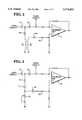
- FIG. 1is circuit diagram showing the principle elements of the invention.
- FIG. 2is a circuit diagram illustrating a coupling circuit suitable for use with the invention.
- FIG. 3is a circuit diagram illustrating another coupling circuit suitable for use with the invention.
- FIG. 4is a circuit diagram of a preferred embodiment of the invention.
- supplying signals from a digitizing gridincludes the case where the signal is taken from the grid per se (U.S. Pat. Nos. 4,644,102 and 5,124,509) or from a stylus inductively, capacitively, or otherwise coupled to the grid (U.S. Pat. No. 3,732,369).
- a digitizing grid 10is coupled, via connectors 15a and 17, to an amplifier 16 which includes suitable input and feedback resistors in a manner well known in the art.
- a transparent conductive shield 12is interposed between the digitizing grid 10 and an image plane 14.
- the image plane 14 and a light source 19can be any type of image source or image generator, e.g., a television screen or a computer monitor screen. It is well known that such image generators produce substantial amounts of electrical noise interference which prior art grounded plates cannot shield.
- the shield 12 and the digitizing grid 10are spaced so that electrostatic noise 13 passing through the shield 12 to the digitizing grid 10 will be substantially congruent or similar to the noise intercepted by the shield 10.
- the distance of the spacing between the shield 12 and the digitizing grid 10is limited by two principal factors. If the spacing is too small, the shield 12 and the digitizing grid 10 form a capacitor which becomes more effective in passing noise signals the closer they are together. If the spacing is too large, a depth field is created and the resulting parallax distortion will cause misplacement of the pen or probe 11 with respect to the image points being digitized. The spacing appears to be optimal between one and two millimeters.
- the shieldmay even be implemented as a coating on the face of the display 14, e.g., a cathode ray tube face.
- the shield 10may be fabricated from an indium-tin-oxide (ITO) material, such as is used commercially in the manufacture of liquid crystal displays, because of its transparency and electrical characteristics.
- ITOindium-tin-oxide
- the shield 12is coupled to a phase shift network 18 which may be constructed to allow the phase and amplitude of the noise signal from the shield 12 to be adjusted over a desired range.
- the phase-adjusted signal from the network 18is coupled to another input of the amplifier 16 through suitable resistors.
- the signalsare coupled to the amplifier 16 so that the noise signal from the shield 12 is cancelled from the signal from the digitizing grid 10 which includes both noise and information components.
- electrostatic and other electrical noise that are included in the signal from the digitizing grid 10, due principally to the image generator 14,will be similar or congruent to that from the shield 12.
- the noise signals from the image generator 14are somewhat attenuated by passing through the shield 12 but because the shield 12 is not ideal 3/4 having a poor ground impedance 3/4 some noise signals will be passed and picked up on the digitizing grid 10.
- the amplitude of the noise signal taken from the shield 12will normally be larger that its corresponding amplitude on the digitizing grid 10. Differences in the amplitudes of the noise signals taken from the shield 12 and the digitizing grid 10 can be compensated for by amplifying either signal or by adjusting the values of the resistors in the amplifier networks.
- FIGS. 2 and 3Other useful methods of coupling the noise from the shield 10 to the amplifier 16 to cancel the noise in the signal from the digitizing grid 10 are shown in FIGS. 2 and 3.
- the capacitors 21 and 23represent the equivalent capacitances coupling noise to the shield 12 and to the digitizing grid 10 (signal).
- the equivalent resistance of the shieldis represented by the resistor 25 which is coupled to ground through an inductance 27. Therefore, current created by the noise on the shield 12 passes through the inductance 27.
- the current through the inductance 27induces a voltage in a proximate inductance 29 which is coupled to the amplifier 16 through a phase adjusting circuit comprising a capacitor 18a and a resistor 18b.
- the signalhas the same noise coupled thereto by the equivalent capacitance 23 so that the input signal to the inverting input terminal of the amplifier 16 includes the noise.
- the output signal from the amplifier 16does not include the noise since it is removed from the signal by coupling it to the noninverting input terminal of the amplifier 16. (The polarities of the input terminals can be reversed.)
- the noisecould be subtracted from the signal by reversing the polarity of the inductance 29 and coupling the signal from the phase adjustment circuit resistively to the inverting input terminal and coupling the noninverting input terminal to ground.
- FIG. 3Another coupling circuit is illustrated in FIG. 3.
- the equivalent capacitors 21 and 23 and the equivalent resistance 25 of the shield 12are the same as described in connection with the circuit of FIG. 2.
- the electric current from the shield 12, i.e., from the resistor 25,is coupled via a capacitor 31 and a resistor 33 (which can be adjustable as shown) to ground.
- the voltage developed across the resistor 33is coupled to the noninverting input terminal of the amplifier 16 via a phase adjusting circuit comprising the capacitor 18a and the resistor 18b, as previously described in connection with the circuit of FIG. 2.
- Coupling the shield to ground through impedancescan create unwanted signals in addition to the noise because the shield 12 is quasi-floating.
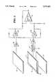
- the shield 12can be grounded on three sides, as shown in FIG. 4, by a ground conductor 41 on the shield.
- the noise potentialcan then be taken from a tap point on the ungrounded side of the shield 12 and coupled to a noise amplifier 47 via a matching circuit 43.
- the matching circuit 43can include a phase adjustment circuit as previously described.
- the noise amplifier 47 and a signal amplifier 45can be inverting operational amplifiers with suitable input and feedback resistors (not shown) or as unity gain amplifiers by coupling the output terminal to the inverting input terminal and coupling the input signal to the noninverting input terminal.
- the latter arrangementprovides an extremely high input impedance to the input noise and signal sources which helps to reduce signal distortion.
- the output signals from the signal amplifier 45 and from the noise amplifier 47are coupled to amplifiers 401 and 403 coupled as a common mode rejection differential amplifier.
- the output signals from the amplifiers 401 and 403are coupled to the output amplifier 16.
- This arrangementnot only supplies a high input impedance for the signals but also rejects common mode noise to prevent distortion of the signals.
Landscapes
- Engineering & Computer Science (AREA)
- General Engineering & Computer Science (AREA)
- Theoretical Computer Science (AREA)
- Human Computer Interaction (AREA)
- Physics & Mathematics (AREA)
- General Physics & Mathematics (AREA)
- Position Input By Displaying (AREA)
- Semiconductor Integrated Circuits (AREA)
- Networks Using Active Elements (AREA)
Abstract
Description
Claims (13)
Priority Applications (5)
| Application Number | Priority Date | Filing Date | Title |
|---|---|---|---|
| US08/317,952US5574262A (en) | 1994-10-04 | 1994-10-04 | Noise cancellation for non-ideal electrostatic shielding |
| DE69514471TDE69514471T2 (en) | 1994-10-04 | 1995-10-02 | Digitizer with noise reduction |
| EP95306976AEP0706147B1 (en) | 1994-10-04 | 1995-10-02 | Digitizer apparatus with noise reduction |
| KR1019950033684AKR100399563B1 (en) | 1994-10-04 | 1995-10-02 | Method and apparatus of noise cancellation for non-ideal electrostatic shielding |
| JP25611295AJP3007560B2 (en) | 1994-10-04 | 1995-10-03 | Tablet device |
Applications Claiming Priority (1)
| Application Number | Priority Date | Filing Date | Title |
|---|---|---|---|
| US08/317,952US5574262A (en) | 1994-10-04 | 1994-10-04 | Noise cancellation for non-ideal electrostatic shielding |
Publications (1)
| Publication Number | Publication Date |
|---|---|
| US5574262Atrue US5574262A (en) | 1996-11-12 |
Family
ID=23235973
Family Applications (1)
| Application Number | Title | Priority Date | Filing Date |
|---|---|---|---|
| US08/317,952Expired - LifetimeUS5574262A (en) | 1994-10-04 | 1994-10-04 | Noise cancellation for non-ideal electrostatic shielding |
Country Status (5)
| Country | Link |
|---|---|
| US (1) | US5574262A (en) |
| EP (1) | EP0706147B1 (en) |
| JP (1) | JP3007560B2 (en) |
| KR (1) | KR100399563B1 (en) |
| DE (1) | DE69514471T2 (en) |
Cited By (34)
| Publication number | Priority date | Publication date | Assignee | Title |
|---|---|---|---|---|
| US5786668A (en)* | 1995-10-27 | 1998-07-28 | Samsung Electronics Co., Ltd. | Electromagnetic field shielding circuit for a display |
| US5798756A (en)* | 1994-12-26 | 1998-08-25 | Sharp Kabushiki Kaisha | Coordinate detection device capable of obviating the need of forming closed loop in electrodes thereof |
| US5859392A (en)* | 1996-02-09 | 1999-01-12 | Lsi Logic Corporation | Method and apparatus for reducing noise in an electrostatic digitizing tablet |
| US5990865A (en)* | 1997-01-06 | 1999-11-23 | Gard; Matthew Davis | Computer interface device |
| US6081259A (en)* | 1997-11-25 | 2000-06-27 | Lsi Logic Corporation | Method and apparatus for reducing noise in an electrostatic digitizer |
| US6473074B1 (en)* | 1998-12-16 | 2002-10-29 | Fujitsu Takamisawa Component Limited | Coordinate data input device |
| US6489575B2 (en)* | 1998-08-14 | 2002-12-03 | Samsung Electronics Co., Ltd. | Sensor panel position coordinates signal detecting circuit |
| US20030010544A1 (en)* | 2001-07-10 | 2003-01-16 | Ching-Chuan Chao | Low EMI digitizer tablet |
| KR100469355B1 (en)* | 2002-11-14 | 2005-02-02 | 엘지.필립스 엘시디 주식회사 | touch panel for display device |
| US20050189154A1 (en)* | 2004-02-27 | 2005-09-01 | Haim Perski | Noise reduction in digitizer system |
| US20070001681A1 (en)* | 2005-06-29 | 2007-01-04 | Alps Electric Co., Ltd. | Input device |
| US20080180407A1 (en)* | 2007-01-30 | 2008-07-31 | Seiko Epson Corporation | Input-capable display device |
| US20080238881A1 (en)* | 2007-03-27 | 2008-10-02 | N-Trig Ltd. | Shield for a digitizer sensor |
| US20080278451A1 (en)* | 2007-05-07 | 2008-11-13 | Samsung Electronics Co., Ltd. | Touch-panel-integrated liquid crystal display and method of driving the same |
| US20090128511A1 (en)* | 2007-11-19 | 2009-05-21 | Microsoft Corporation | Pointing and data entry input device |
| US20100328266A1 (en)* | 2008-03-31 | 2010-12-30 | Kazuto Yamauchi | Electrostatic capacitive touch sensor device |
| US20130285965A1 (en)* | 2009-09-08 | 2013-10-31 | Samsung Display Co., Ltd. | Display device including touch panel device, and coupling-noise eliminating method |
| US20170010750A1 (en)* | 2007-01-05 | 2017-01-12 | Apple Inc. | Touch screen stack-ups |
| US9823774B2 (en) | 2016-02-23 | 2017-11-21 | Microsoft Technology Licensing, Llc | Noise reduction in a digitizer system |
| US10095361B2 (en) | 2015-03-18 | 2018-10-09 | Microsoft Technology Licensing, Llc | Stylus detection with capacitive based digitizer sensor |
| US10296146B2 (en) | 2015-12-22 | 2019-05-21 | Microsoft Technology Licensing, Llc | System and method for detecting grip of a touch enabled device |
| US10331259B2 (en) | 2004-05-06 | 2019-06-25 | Apple Inc. | Multipoint touchscreen |
| US10372282B2 (en) | 2016-12-01 | 2019-08-06 | Apple Inc. | Capacitive coupling reduction in touch sensor panels |
| US10409434B2 (en) | 2010-12-22 | 2019-09-10 | Apple Inc. | Integrated touch screens |
| US10423268B2 (en) | 2015-12-22 | 2019-09-24 | Microsoft Technology Licensing, Llc | System and method for detecting grounding state of a touch enabled computing device |
| US10474287B2 (en) | 2007-01-03 | 2019-11-12 | Apple Inc. | Double-sided touch-sensitive panel with shield and drive combined layer |
| US10616349B2 (en) | 2018-05-01 | 2020-04-07 | Microsoft Technology Licensing, Llc | Hybrid sensor centric recommendation engine |
| US10678348B2 (en) | 2018-03-12 | 2020-06-09 | Microsoft Technology Licensing, Llc | Touch detection on an ungrounded pen enabled device |
| US10955978B2 (en) | 2016-09-23 | 2021-03-23 | Apple Inc. | Touch sensor panel with top and/or bottom shielding |
| US10976846B2 (en) | 2006-06-09 | 2021-04-13 | Apple Inc. | Touch screen liquid crystal display |
| US11460964B2 (en) | 2011-10-20 | 2022-10-04 | Apple Inc. | Opaque thin film passivation |
| US11789561B2 (en) | 2021-09-24 | 2023-10-17 | Apple Inc. | Architecture for differential drive and sense touch technology |
| US12197679B2 (en) | 2022-05-06 | 2025-01-14 | Apple Inc. | Touch screen shield layer with ring and tapping points |
| US12260045B2 (en) | 2021-09-24 | 2025-03-25 | Apple Inc. | Architecture for differential drive and sense for touch sensor panel |
Families Citing this family (11)
| Publication number | Priority date | Publication date | Assignee | Title |
|---|---|---|---|---|
| US5841427A (en)* | 1995-12-22 | 1998-11-24 | Symbios, Inc. | Method and apparatus for canceling an offset signal in an electrostatic digitizing tablet |
| GB2373581B (en)* | 2001-03-20 | 2004-11-10 | Eturbotouch Technology Inc | Touch screen capable of isolating noise signals |
| US7678346B2 (en) | 2003-01-30 | 2010-03-16 | Gm Global Technology Operations, Inc. | Dual function CO clean-up/sorber unit |
| KR101237640B1 (en)* | 2008-01-29 | 2013-02-27 | (주)멜파스 | Touchscreen apparatus having structure for preventing forming of parasitic capacitance |
| US9927924B2 (en) | 2008-09-26 | 2018-03-27 | Apple Inc. | Differential sensing for a touch panel |
| US8614690B2 (en) | 2008-09-26 | 2013-12-24 | Apple Inc. | Touch sensor panel using dummy ground conductors |
| US9164620B2 (en) | 2010-06-07 | 2015-10-20 | Apple Inc. | Touch sensing error compensation |
| KR20130005660A (en)* | 2011-07-07 | 2013-01-16 | 삼성전자주식회사 | Touch screen panel liquid crystal display device |
| FR2988553B1 (en)* | 2012-03-23 | 2015-03-27 | Fogale Nanotech | CAPACITIVE DETECTION DEVICE INTEGRATING A METAL TRACK ON A TRANSPARENT GUARD. |
| US9671913B2 (en) | 2015-05-11 | 2017-06-06 | Microsoft Technology Licensing, Llc | Capacitive display device |
| CN113311959B (en)* | 2021-05-18 | 2023-01-17 | 维沃移动通信有限公司 | Display module and electronic device |
Citations (23)
| Publication number | Priority date | Publication date | Assignee | Title |
|---|---|---|---|---|
| US3732369A (en)* | 1971-04-05 | 1973-05-08 | Welland Investment Trust | Coordinate digitizer system |
| US3974332A (en)* | 1974-12-03 | 1976-08-10 | Pentel Kabushiki Kaisha | Tablet for use in a coordinate digitizer |
| US4185165A (en)* | 1978-07-03 | 1980-01-22 | Talos Systems, Inc. | Low noise system and method for sequentially sensing induced signals in digitizer grid conductors |
| US4456787A (en)* | 1982-07-06 | 1984-06-26 | Scriptel Corporation | Electrographic system and method |
| US4497977A (en)* | 1983-03-03 | 1985-02-05 | Kabushiki Kaisha Daini Seikosha | Automatic coordinate determining device having electrostatic shielding |
| US4631355A (en)* | 1984-12-18 | 1986-12-23 | At&T Bell Laboratories | Telautograph system |
| US4636582A (en)* | 1983-08-31 | 1987-01-13 | Toppan Moore Co., Ltd. | Signal input sheet having a conductive shield layer |
| US4644102A (en)* | 1985-03-29 | 1987-02-17 | Pencept, Inc. | Digitizing tablet system |
| US4736073A (en)* | 1986-02-10 | 1988-04-05 | Sanders Associates, Inc. | Noise-canceling system for a digitizing tablet |
| US4788384A (en)* | 1986-12-18 | 1988-11-29 | Centre National De La Recherche Scientifique | Device for two-dimensional localization of events that generate current on a resistive surface |
| US4853497A (en)* | 1988-06-20 | 1989-08-01 | Calcomp Inc. | Shielding techique for digitizers |
| US4859814A (en)* | 1988-08-29 | 1989-08-22 | Kurta Corporation | Noise cancellation in digitizing system and method |
| US4956526A (en)* | 1989-07-18 | 1990-09-11 | Kabushikikaisha Wacom | Digitizer having flat tablet with magnetic shield plate |
| US5008497A (en)* | 1990-03-22 | 1991-04-16 | Asher David J | Touch controller |
| US5010213A (en)* | 1988-12-29 | 1991-04-23 | Toppan Moore Company, Ltd. | Signal input sheet |
| US5083118A (en)* | 1990-04-16 | 1992-01-21 | Pentel Kabushiki Kaisha | Transparent coordinate input apparatus for electrostatic capacity coupling system |
| US5124509A (en)* | 1991-01-15 | 1992-06-23 | Calcomp, Inc. | Digitizer with capacitive and inductive coupling |
| US5136125A (en)* | 1991-05-06 | 1992-08-04 | International Business Machines Corporation | Sensor grid for an electromagnetic digitizer tablet |
| US5162782A (en)* | 1989-08-28 | 1992-11-10 | Mitsubishi Denki Kabushiki Kaisha | Display device with coordinate input function |
| US5177328A (en)* | 1990-06-28 | 1993-01-05 | Kabushiki Kaisha Toshiba | Information processing apparatus |
| US5218174A (en)* | 1991-10-01 | 1993-06-08 | Kurta Corporation | Low power cordless magnetic field digitizer with differential grid sensing and synchronous position demodulation |
| US5218173A (en)* | 1991-10-17 | 1993-06-08 | Ibm Corporation | Shielding materials for electromagnetic digitizers |
| EP0589498A1 (en)* | 1992-08-12 | 1994-03-30 | Koninklijke Philips Electronics N.V. | Electronic circuitry rendered immune to EM noise of display |
Family Cites Families (2)
| Publication number | Priority date | Publication date | Assignee | Title |
|---|---|---|---|---|
| JP2988779B2 (en)* | 1992-05-20 | 1999-12-13 | シャープ株式会社 | Tablet device with display function |
| JP3003895B2 (en)* | 1992-09-09 | 2000-01-31 | 川崎重工業株式会社 | Laser processing equipment |
- 1994
- 1994-10-04USUS08/317,952patent/US5574262A/ennot_activeExpired - Lifetime
- 1995
- 1995-10-02KRKR1019950033684Apatent/KR100399563B1/ennot_activeExpired - Fee Related
- 1995-10-02DEDE69514471Tpatent/DE69514471T2/ennot_activeExpired - Fee Related
- 1995-10-02EPEP95306976Apatent/EP0706147B1/ennot_activeExpired - Lifetime
- 1995-10-03JPJP25611295Apatent/JP3007560B2/ennot_activeExpired - Fee Related
Patent Citations (23)
| Publication number | Priority date | Publication date | Assignee | Title |
|---|---|---|---|---|
| US3732369A (en)* | 1971-04-05 | 1973-05-08 | Welland Investment Trust | Coordinate digitizer system |
| US3974332A (en)* | 1974-12-03 | 1976-08-10 | Pentel Kabushiki Kaisha | Tablet for use in a coordinate digitizer |
| US4185165A (en)* | 1978-07-03 | 1980-01-22 | Talos Systems, Inc. | Low noise system and method for sequentially sensing induced signals in digitizer grid conductors |
| US4456787A (en)* | 1982-07-06 | 1984-06-26 | Scriptel Corporation | Electrographic system and method |
| US4497977A (en)* | 1983-03-03 | 1985-02-05 | Kabushiki Kaisha Daini Seikosha | Automatic coordinate determining device having electrostatic shielding |
| US4636582A (en)* | 1983-08-31 | 1987-01-13 | Toppan Moore Co., Ltd. | Signal input sheet having a conductive shield layer |
| US4631355A (en)* | 1984-12-18 | 1986-12-23 | At&T Bell Laboratories | Telautograph system |
| US4644102A (en)* | 1985-03-29 | 1987-02-17 | Pencept, Inc. | Digitizing tablet system |
| US4736073A (en)* | 1986-02-10 | 1988-04-05 | Sanders Associates, Inc. | Noise-canceling system for a digitizing tablet |
| US4788384A (en)* | 1986-12-18 | 1988-11-29 | Centre National De La Recherche Scientifique | Device for two-dimensional localization of events that generate current on a resistive surface |
| US4853497A (en)* | 1988-06-20 | 1989-08-01 | Calcomp Inc. | Shielding techique for digitizers |
| US4859814A (en)* | 1988-08-29 | 1989-08-22 | Kurta Corporation | Noise cancellation in digitizing system and method |
| US5010213A (en)* | 1988-12-29 | 1991-04-23 | Toppan Moore Company, Ltd. | Signal input sheet |
| US4956526A (en)* | 1989-07-18 | 1990-09-11 | Kabushikikaisha Wacom | Digitizer having flat tablet with magnetic shield plate |
| US5162782A (en)* | 1989-08-28 | 1992-11-10 | Mitsubishi Denki Kabushiki Kaisha | Display device with coordinate input function |
| US5008497A (en)* | 1990-03-22 | 1991-04-16 | Asher David J | Touch controller |
| US5083118A (en)* | 1990-04-16 | 1992-01-21 | Pentel Kabushiki Kaisha | Transparent coordinate input apparatus for electrostatic capacity coupling system |
| US5177328A (en)* | 1990-06-28 | 1993-01-05 | Kabushiki Kaisha Toshiba | Information processing apparatus |
| US5124509A (en)* | 1991-01-15 | 1992-06-23 | Calcomp, Inc. | Digitizer with capacitive and inductive coupling |
| US5136125A (en)* | 1991-05-06 | 1992-08-04 | International Business Machines Corporation | Sensor grid for an electromagnetic digitizer tablet |
| US5218174A (en)* | 1991-10-01 | 1993-06-08 | Kurta Corporation | Low power cordless magnetic field digitizer with differential grid sensing and synchronous position demodulation |
| US5218173A (en)* | 1991-10-17 | 1993-06-08 | Ibm Corporation | Shielding materials for electromagnetic digitizers |
| EP0589498A1 (en)* | 1992-08-12 | 1994-03-30 | Koninklijke Philips Electronics N.V. | Electronic circuitry rendered immune to EM noise of display |
Cited By (54)
| Publication number | Priority date | Publication date | Assignee | Title |
|---|---|---|---|---|
| US5798756A (en)* | 1994-12-26 | 1998-08-25 | Sharp Kabushiki Kaisha | Coordinate detection device capable of obviating the need of forming closed loop in electrodes thereof |
| US5786668A (en)* | 1995-10-27 | 1998-07-28 | Samsung Electronics Co., Ltd. | Electromagnetic field shielding circuit for a display |
| US5859392A (en)* | 1996-02-09 | 1999-01-12 | Lsi Logic Corporation | Method and apparatus for reducing noise in an electrostatic digitizing tablet |
| US7333089B1 (en) | 1997-01-06 | 2008-02-19 | Matthew Davis Gard | Computer interface device |
| US5990865A (en)* | 1997-01-06 | 1999-11-23 | Gard; Matthew Davis | Computer interface device |
| US6081259A (en)* | 1997-11-25 | 2000-06-27 | Lsi Logic Corporation | Method and apparatus for reducing noise in an electrostatic digitizer |
| US6489575B2 (en)* | 1998-08-14 | 2002-12-03 | Samsung Electronics Co., Ltd. | Sensor panel position coordinates signal detecting circuit |
| US6473074B1 (en)* | 1998-12-16 | 2002-10-29 | Fujitsu Takamisawa Component Limited | Coordinate data input device |
| US20030010544A1 (en)* | 2001-07-10 | 2003-01-16 | Ching-Chuan Chao | Low EMI digitizer tablet |
| KR100469355B1 (en)* | 2002-11-14 | 2005-02-02 | 엘지.필립스 엘시디 주식회사 | touch panel for display device |
| US7995036B2 (en)* | 2004-02-27 | 2011-08-09 | N-Trig Ltd. | Noise reduction in digitizer system |
| US20050189154A1 (en)* | 2004-02-27 | 2005-09-01 | Haim Perski | Noise reduction in digitizer system |
| US9372575B2 (en) | 2004-02-27 | 2016-06-21 | Microsoft Technology Licensing, Llc | Noise reduction in digitizer system |
| US9164618B2 (en) | 2004-02-27 | 2015-10-20 | Microsoft Technology Licensing, Llc | Noise reduction in digitizer system |
| US8648830B2 (en) | 2004-02-27 | 2014-02-11 | N-Trig Ltd. | Noise reduction in digitizer system |
| US10331259B2 (en) | 2004-05-06 | 2019-06-25 | Apple Inc. | Multipoint touchscreen |
| US11604547B2 (en) | 2004-05-06 | 2023-03-14 | Apple Inc. | Multipoint touchscreen |
| US10908729B2 (en) | 2004-05-06 | 2021-02-02 | Apple Inc. | Multipoint touchscreen |
| US7279904B2 (en)* | 2005-06-29 | 2007-10-09 | Alps Electric Co., Ltd. | Input device |
| US20070001681A1 (en)* | 2005-06-29 | 2007-01-04 | Alps Electric Co., Ltd. | Input device |
| US10976846B2 (en) | 2006-06-09 | 2021-04-13 | Apple Inc. | Touch screen liquid crystal display |
| US11175762B2 (en) | 2006-06-09 | 2021-11-16 | Apple Inc. | Touch screen liquid crystal display |
| US11886651B2 (en) | 2006-06-09 | 2024-01-30 | Apple Inc. | Touch screen liquid crystal display |
| US11112904B2 (en) | 2007-01-03 | 2021-09-07 | Apple Inc. | Double-sided touch-sensitive panel with shield and drive combined layer |
| US10474287B2 (en) | 2007-01-03 | 2019-11-12 | Apple Inc. | Double-sided touch-sensitive panel with shield and drive combined layer |
| US10521065B2 (en)* | 2007-01-05 | 2019-12-31 | Apple Inc. | Touch screen stack-ups |
| US20170010750A1 (en)* | 2007-01-05 | 2017-01-12 | Apple Inc. | Touch screen stack-ups |
| TWI476474B (en)* | 2007-01-30 | 2015-03-11 | Japan Display West Inc | Input-capable display device |
| US20080180407A1 (en)* | 2007-01-30 | 2008-07-31 | Seiko Epson Corporation | Input-capable display device |
| US9891458B2 (en) | 2007-01-30 | 2018-02-13 | Japan Display Inc. | Input-capable display device |
| US9069401B2 (en)* | 2007-01-30 | 2015-06-30 | Japan Display Inc. | Input-capable display device |
| US20080238881A1 (en)* | 2007-03-27 | 2008-10-02 | N-Trig Ltd. | Shield for a digitizer sensor |
| US20080278451A1 (en)* | 2007-05-07 | 2008-11-13 | Samsung Electronics Co., Ltd. | Touch-panel-integrated liquid crystal display and method of driving the same |
| US20090128511A1 (en)* | 2007-11-19 | 2009-05-21 | Microsoft Corporation | Pointing and data entry input device |
| US8174508B2 (en)* | 2007-11-19 | 2012-05-08 | Microsoft Corporation | Pointing and data entry input device |
| US8654097B2 (en)* | 2008-03-31 | 2014-02-18 | Mitsubishi Jidosha Kogyo Kabushiki Kaisha | Electrostatic capacitive touch sensor device |
| CN101878593B (en)* | 2008-03-31 | 2014-01-29 | 三菱自动车工业株式会社 | Electrostatic capacitive touch sensor device |
| US20100328266A1 (en)* | 2008-03-31 | 2010-12-30 | Kazuto Yamauchi | Electrostatic capacitive touch sensor device |
| US20130285965A1 (en)* | 2009-09-08 | 2013-10-31 | Samsung Display Co., Ltd. | Display device including touch panel device, and coupling-noise eliminating method |
| US9535526B2 (en) | 2009-09-08 | 2017-01-03 | Samsung Display Co., Ltd. | Display device including touch panel device, and coupling-noise eliminating method |
| US10409434B2 (en) | 2010-12-22 | 2019-09-10 | Apple Inc. | Integrated touch screens |
| US11460964B2 (en) | 2011-10-20 | 2022-10-04 | Apple Inc. | Opaque thin film passivation |
| US10095361B2 (en) | 2015-03-18 | 2018-10-09 | Microsoft Technology Licensing, Llc | Stylus detection with capacitive based digitizer sensor |
| US10296146B2 (en) | 2015-12-22 | 2019-05-21 | Microsoft Technology Licensing, Llc | System and method for detecting grip of a touch enabled device |
| US10423268B2 (en) | 2015-12-22 | 2019-09-24 | Microsoft Technology Licensing, Llc | System and method for detecting grounding state of a touch enabled computing device |
| US9823774B2 (en) | 2016-02-23 | 2017-11-21 | Microsoft Technology Licensing, Llc | Noise reduction in a digitizer system |
| US10955978B2 (en) | 2016-09-23 | 2021-03-23 | Apple Inc. | Touch sensor panel with top and/or bottom shielding |
| US10606430B2 (en) | 2016-12-01 | 2020-03-31 | Apple Inc. | Capacitive coupling reduction in touch sensor panels |
| US10372282B2 (en) | 2016-12-01 | 2019-08-06 | Apple Inc. | Capacitive coupling reduction in touch sensor panels |
| US10678348B2 (en) | 2018-03-12 | 2020-06-09 | Microsoft Technology Licensing, Llc | Touch detection on an ungrounded pen enabled device |
| US10616349B2 (en) | 2018-05-01 | 2020-04-07 | Microsoft Technology Licensing, Llc | Hybrid sensor centric recommendation engine |
| US11789561B2 (en) | 2021-09-24 | 2023-10-17 | Apple Inc. | Architecture for differential drive and sense touch technology |
| US12260045B2 (en) | 2021-09-24 | 2025-03-25 | Apple Inc. | Architecture for differential drive and sense for touch sensor panel |
| US12197679B2 (en) | 2022-05-06 | 2025-01-14 | Apple Inc. | Touch screen shield layer with ring and tapping points |
Also Published As
| Publication number | Publication date |
|---|---|
| KR960015343A (en) | 1996-05-22 |
| EP0706147A3 (en) | 1996-05-01 |
| JPH08147090A (en) | 1996-06-07 |
| KR100399563B1 (en) | 2004-03-26 |
| EP0706147A2 (en) | 1996-04-10 |
| DE69514471D1 (en) | 2000-02-17 |
| DE69514471T2 (en) | 2000-07-13 |
| JP3007560B2 (en) | 2000-02-07 |
| EP0706147B1 (en) | 2000-01-12 |
Similar Documents
| Publication | Publication Date | Title |
|---|---|---|
| US5574262A (en) | Noise cancellation for non-ideal electrostatic shielding | |
| JP3237629B2 (en) | Direct contact type touch panel device | |
| US5274198A (en) | Printed conductive ink electrostatic shield for electromagnetic digitizers | |
| KR101300958B1 (en) | Touch screen having reduced susceptibility to radio frequency interference | |
| US4788384A (en) | Device for two-dimensional localization of events that generate current on a resistive surface | |
| US9430105B2 (en) | Frequency independent offset cancellation scheme in touch receiver channel | |
| US5841427A (en) | Method and apparatus for canceling an offset signal in an electrostatic digitizing tablet | |
| US6133906A (en) | Display-integrated stylus detection system | |
| US20160034102A1 (en) | Method of multi-zone capacitive sensing, device and apparatus implementing the method | |
| US20080238881A1 (en) | Shield for a digitizer sensor | |
| EP0712090B1 (en) | Touch sensor input system for a computer display | |
| CN106575183A (en) | Capacitive-based touch apparatus and method with reduced interference | |
| EP0610262A1 (en) | See-through digitizer with clear conductive grid | |
| JPH061429B2 (en) | Position measuring device for touch panel system | |
| CA2874744A1 (en) | Electrode testing apparatus | |
| CN107077241A (en) | The coordinate entering device of touch detection performance with raising | |
| JP5035205B2 (en) | Touch panel device | |
| JP2001099609A (en) | Parasitic signal removal type touch panel device | |
| JP3864512B2 (en) | Capacitive coupling type coordinate input device using non-directly connected pen case | |
| JPH0354624A (en) | Position measuring instrument for touch panel | |
| JPS6074014A (en) | Driving device of coordinate detection panel | |
| Abe et al. | Reduction of noise induced by power supply lines using phase-locked loop | |
| JPH0916330A (en) | Transparent digitizer for display | |
| JPH07210294A (en) | Information processing equipment | |
| JPS5828287Y2 (en) | coordinate reading device |
Legal Events
| Date | Code | Title | Description |
|---|---|---|---|
| AS | Assignment | Owner name:AT&T GLOBAL INFORMATION SOLUTIONS COMPANY, OHIO Free format text:ASSIGNMENT OF ASSIGNORS INTEREST;ASSIGNOR:PETTY, WILLIAM K.;REEL/FRAME:007192/0677 Effective date:19940930 | |
| AS | Assignment | Owner name:HYUNDAI ELECTRONICS AMERICA Free format text:ASSIGNMENT OF ASSIGNORS INTEREST;ASSIGNOR:AT&T GLOBAL INFORMATION SOLUTIONS COMPANY (FORMERLY KNOWN AS NCR CORPORATION);REEL/FRAME:007408/0104 Effective date:19950215 | |
| AS | Assignment | Owner name:SYMBIOS LOGIC INC., COLORADO Free format text:ASSIGNMENT OF ASSIGNORS INTEREST;ASSIGNOR:HYUNDAI ELECTRONICS AMERICA;REEL/FRAME:007629/0431 Effective date:19950818 | |
| STCF | Information on status: patent grant | Free format text:PATENTED CASE | |
| AS | Assignment | Owner name:SYMBIOS, INC ., COLORADO Free format text:CHANGE OF NAME;ASSIGNOR:SYMBIOS LOGIC INC.;REEL/FRAME:009089/0936 Effective date:19971210 | |
| AS | Assignment | Owner name:LEHMAN COMMERCIAL PAPER INC., AS ADMINISTRATIVE AG Free format text:SECURITY AGREEMENT;ASSIGNORS:HYUNDAI ELECTRONICS AMERICA, A CORP. OF CALIFORNIA;SYMBIOS, INC., A CORP. OF DELAWARE;REEL/FRAME:009396/0441 Effective date:19980226 | |
| AS | Assignment | Owner name:HYUNDAI ELECTRONICS AMERICA, CALIFORNIA Free format text:TERMINATION AND LICENSE AGREEMENT;ASSIGNOR:SYMBIOS, INC.;REEL/FRAME:009596/0539 Effective date:19980806 | |
| FEPP | Fee payment procedure | Free format text:PAYOR NUMBER ASSIGNED (ORIGINAL EVENT CODE: ASPN); ENTITY STATUS OF PATENT OWNER: LARGE ENTITY | |
| FPAY | Fee payment | Year of fee payment:4 | |
| FPAY | Fee payment | Year of fee payment:8 | |
| AS | Assignment | Owner name:HYNIX SEMICONDUCTOR AMERICA INC., CALIFORNIA Free format text:CHANGE OF NAME;ASSIGNOR:HYUNDAI ELECTRONICS AMERICA;REEL/FRAME:015246/0599 Effective date:20010412 Owner name:HYNIX SEMICONDUCTOR INC., KOREA, REPUBLIC OF Free format text:ASSIGNMENT OF ASSIGNORS INTEREST;ASSIGNOR:HYNIX SEMICONDUCTOR AMERICA, INC.;REEL/FRAME:015279/0556 Effective date:20040920 | |
| AS | Assignment | Owner name:MAGNACHIP SEMICONDUCTOR, LTD., KOREA, REPUBLIC OF Free format text:ASSIGNMENT OF ASSIGNORS INTEREST;ASSIGNOR:HYNIX SEMICONDUCTOR, INC.;REEL/FRAME:016216/0649 Effective date:20041004 | |
| AS | Assignment | Owner name:U.S. BANK NATIONAL ASSOCIATION, AS COLLATERAL TRUS Free format text:SECURITY INTEREST;ASSIGNOR:MAGNACHIP SEMICONDUCTOR, LTD.;REEL/FRAME:016470/0530 Effective date:20041223 | |
| AS | Assignment | Owner name:SYMBIOS, INC., COLORADO Free format text:RELEASE OF SECURITY INTEREST;ASSIGNOR:LEHMAN COMMERICAL PAPER INC.;REEL/FRAME:016602/0895 Effective date:20050107 Owner name:HYUNDAI ELECTRONICS AMERICA, CALIFORNIA Free format text:RELEASE OF SECURITY INTEREST;ASSIGNOR:LEHMAN COMMERICAL PAPER INC.;REEL/FRAME:016602/0895 Effective date:20050107 | |
| FPAY | Fee payment | Year of fee payment:12 | |
| REMI | Maintenance fee reminder mailed | ||
| AS | Assignment | Owner name:TAIWAN SEMICONDUCTOR MANUFACTURING CO., LTD., TAIW Free format text:ASSIGNMENT OF ASSIGNORS INTEREST;ASSIGNORS:NCR CORPORATION;MAGNACHIP SEMICONDUCTOR, LTD.;REEL/FRAME:021398/0702;SIGNING DATES FROM 20071114 TO 20071115 |