US5572691A - Apparatus and method for providing multiple data streams from stored data using dual memory buffers - Google Patents
Apparatus and method for providing multiple data streams from stored data using dual memory buffersDownload PDFInfo
- Publication number
- US5572691A US5572691AUS08/047,541US4754193AUS5572691AUS 5572691 AUS5572691 AUS 5572691AUS 4754193 AUS4754193 AUS 4754193AUS 5572691 AUS5572691 AUS 5572691A
- Authority
- US
- United States
- Prior art keywords
- pixels
- data
- memory bank
- output
- bytes
- Prior art date
- Legal status (The legal status is an assumption and is not a legal conclusion. Google has not performed a legal analysis and makes no representation as to the accuracy of the status listed.)
- Expired - Lifetime
Links
Images


Classifications
- H—ELECTRICITY
- H04—ELECTRIC COMMUNICATION TECHNIQUE
- H04N—PICTORIAL COMMUNICATION, e.g. TELEVISION
- H04N5/00—Details of television systems
- H04N5/76—Television signal recording
- H04N5/907—Television signal recording using static stores, e.g. storage tubes or semiconductor memories
- H—ELECTRICITY
- H04—ELECTRIC COMMUNICATION TECHNIQUE
- H04N—PICTORIAL COMMUNICATION, e.g. TELEVISION
- H04N19/00—Methods or arrangements for coding, decoding, compressing or decompressing digital video signals
- H04N19/60—Methods or arrangements for coding, decoding, compressing or decompressing digital video signals using transform coding
- H04N19/61—Methods or arrangements for coding, decoding, compressing or decompressing digital video signals using transform coding in combination with predictive coding
- H—ELECTRICITY
- H04—ELECTRIC COMMUNICATION TECHNIQUE
- H04N—PICTORIAL COMMUNICATION, e.g. TELEVISION
- H04N19/00—Methods or arrangements for coding, decoding, compressing or decompressing digital video signals
- H04N19/85—Methods or arrangements for coding, decoding, compressing or decompressing digital video signals using pre-processing or post-processing specially adapted for video compression
Definitions
- the present inventionrelates to the communication of digital data and more particularly to the processing of successive frames of digital information to provide a plurality of different data streams from each frame.
- the inventionis particularly applicable to the communication of digital video signals, in which a plurality of different scanning formats are needed for different processing functions.
- NTSCNational Television System Committee
- PALPhase Alternating Line
- SECAMSequential Color And Memory
- Digital transmission of television signalscan deliver video and audio services of much higher quality than analog techniques.
- Digital transmission schemesare particularly advantageous for signals that are broadcast by satellite to cable television affiliates and/or directly to home satellite television receivers. It is expected that digital television transmitter and receiver systems will replace existing analog systems just as digital compact discs have largely replaced analog phonograph records in the audio industry.
- HDTVhigh definition television
- a subscriberreceives the digital data stream via a receiver/descrambler that provides video, audio, and data to the subscriber.
- a receiver/descramblerthat provides video, audio, and data to the subscriber.
- the video portion of a television signalcomprises a sequence of video "frames" that together provide a moving picture.
- each line of a video frameis defined by a sequence of digital data referred to as "pixels.”
- a large amount of datais required to define each video frame of a television signal. For example, 7.4 megabits of data is required to provide one video frame at NTSC resolution. This assumes a 640 pixel by 480 line display is used with 8 bits of intensity value for each of the primary colors red, green and blue.
- High definition televisionrequires substantially more data to provide each video frame. In order to manage this amount of data, particularly for HDTV applications, the data must be compressed.
- Video compression techniquesenable the efficient transmission of digital video signals over conventional communication channels. Such techniques use compression algorithms that take advantage of the correlation among adjacent pixels in order to derive a more efficient representation of the important information in a video signal.
- transform codersOne of the most effective and frequently used classes of algorithms for video compression is referred to as "transform coders.”
- blocks of videoare linearly and successively transformed into a new domain with properties significantly different from the image intensity domain.
- the blocksmay be nonoverlapping, as in the case of the discrete cosine transform (DCT), or overlapping as in the case of the lapped orthogonal transform (LOT).
- DCTdiscrete cosine transform
- LOTlapped orthogonal transform
- Systems using the DCTare described in Chen and Pratt, "Scene Adaptive Coder", IEEE Transactions on Communications, Vol. COM-32, No. 3, Mar. 1984, and in U.S. Pat. No.4,791,598 entitled “Two-Dimensional Discrete Cosine Transform Processor” to Liou, et al., issued Dec. 13, 1988.
- a system using the LOTis described in Malvar and Staelin, "The LOT: Transform Coding Without Blocking Effects
- Video transformsare used to reduce the correlation that exists among samples of image intensity (pixels). Thus, these transforms concentrate the energy into a relatively small number of transform coefficients. Most common transforms have properties that easily permit the quantification of coefficients based on a model of the human visual system. For example, the DCT produces coefficients with amplitudes that are representative of the energy in a particular band of the frequency spectrum. Therefore, it is possible to utilize the fact that the human viewer is more critical of errors in the low frequency regions of an image than in the high frequency or detailed areas. In general, the high frequency coefficients are always quantized more coarsely than the low frequencies.
- the output of the DCTis a matrix of coefficients which represent energy in the two-dimensional frequency domain. Most of the energy is concentrated at the upper left corner of the matrix, which is the low frequency region. If the coefficients are scanned in a zigzag manner, starting in the upper left corner, the resultant sequence will contain long strings of zeros, especially toward the end of the sequence.
- One of the major objectives of the DCT compression algorithmis to create zeros and to bunch them together for efficient coding.
- the transform coefficientsare communicated in n ⁇ n blocks of coefficients, such as 8 ⁇ 8 or 16 ⁇ 16 blocks.
- inverse transformit is necessary to reorder them at the receiver, using the same block format scanning order (e.g., zigzag scanning) used at the transmitter.
- the incoming video data for a current frameis stored in a first memory bank while the data from a prior frame is read out from a second memory bank.
- the buffersare swapped so that the memory bank that just received a frame of data will output that data and the other memory bank will receive the next frame of data. This technique is useful in converting the scanning format of the incoming video data to a format required for subsequent processing.
- additional memory bankshave been provided.
- the provision of additional memory banksincreases the memory and associated hardware requirements to a point that can render the system design rather complex and expensive.
- the present inventionprovides a dual memory buffer scheme for outputting multiple data streams having the aforementioned advantages.
- apparatusfor storing successive frames containing bytes of digital information and subsequently outputting N data streams for each frame.
- the bytescan be of any length (e.g., 8 bits) depending on the application.
- Each of the N data streamsprovides the bytes for the frame in a different order for subsequent processing.
- the framesare frames of video data (i.e., pixels)
- one data streamcan provide the pixels for DCT processing in a block format and another data stream can provide the pixels for film mode processing on a line-by-line basis.
- the apparatuscomprises first and second memory banks for storing alternate frames.
- the first memory bankis adapted to store bytes from an incoming frame while the second memory bank outputs bytes from a previous frame, and vice versa.
- Meansare provided for controlling the inputting and outputting of bytes to and from the first and second memory banks.
- the memory banksare responsive to read and write strobes and addresses provided by the controlling means for (i) storing incoming frame data in an order determined by write addresses at a rate of N bytes per write strobe and (ii) outputting N bytes of frame data specified by a read address for a next successive one of the N different data streams every read strobe.
- One write strobeoccurs for every N read strobes.
- Meansare provided for buffering the frame data output from the memory banks for each of the N different data streams to provide one byte per read strobe in each of the data streams.
- the controlling meanscan comprise a write address generator and N read address generators for each memory bank.
- Meansare provided for coupling the write address generator for a memory bank to address ports of the memory bank when the memory bank is receiving bytes from an incoming frame for storage.
- Meansare provided for sequentially coupling the different read address generators for a memory bank to address ports of the memory bank when the memory bank is outputting bytes therefrom.
- Meanscan be provided for alternatingly coupling the buffering means to the first and second memory banks to process data from one frame at a time.
- the buffering meanscan comprise N registers, each responsive to a respective enable signal generated by the controlling means for receiving N data bytes at a time output by the memory bank in response to a current read address.
- a data selector associated with each registersequentially outputs each of the N data bytes from the register in response to successive read strobes.
- Each data selectorprovides a continuous stream of data bytes in an order dictated by the read addresses that are current when the register associated with the data selector is enabled.
- the buffering meanscomprise, for each of the memory banks, N registers coupled to the memory bank. Each register is responsive to a respective enable signal generated by the controlling means for receiving N data bytes at a time output by the memory bank in response to a current read address. A data selector associated with each register sequentially outputs each of the N data bytes from the register in response to successive read strobes. Means are provided for multiplexing the data bytes output from corresponding data selectors of the first and second memory banks. The multiplexing means output N continuous streams of data bytes. Each stream provides the data bytes in an order dictated by the read addresses that are current when the registers associated with the data selectors used to form the stream are enabled.
- successive frames of pixel dataare processed to provide N data streams containing the pixel data in different orders.
- Incoming frames of pixel dataare alternately stored in a first memory bank at a rate of N pixels per write cycle while pixel data of a previous frame is output from a second memory bank at a rate of N pixels per read cycle, and vice versa.
- the read cyclehas a rate of N times the write cycle to provide N, N-pixel sets of output pixels per write cycle.
- the pixels output from the memory banks for each of the N setsare buffered to provide the N data streams.
- the memory bank outputting pixel datais newly addressed to provide a set of N pixels for a next successive one of the data streams.
- Apparatusis also provided in accordance with the invention for processing successive frames of pixel data to provide two data streams containing the pixel data in different orders.
- Meansare provided for grouping pixels from an incoming current video frame to provide successive pairs of pixels for storage in a first memory bank at a first clock rate ⁇ .
- Meansare provided for reading stored pairs of pixels of a previous video frame from a second memory bank at a second clock rate 2 ⁇ while the pairs of pixels from the current video frame are being stored in the first memory bank at rate ⁇ .
- the reading meansprovide two pairs of pixels from the previous video frame for each one pair of pixels stored from the current video frame.
- Meansare provided for combining the pairs of pixels provided by the reading means into two data streams. Each data stream provides the pixels from the previous frame in a different order.
- the means for grouping pixelscan comprise a latch for delaying pixels from the incoming video frame by one clock cycle. Means are provided for combining a delayed pixel from the latch with a next successive pixel in the incoming video frame to provide a pair of pixels.
- the means for combining the pairs of pixels provided by the reading means into two data streamscan comprise first and second output registers. Means are provided for inputting every other pair of pixels provided by the reading means into the first output register and for inputting the remaining pairs of pixels provided by the reading means into the second output register. Means are provided for retrieving pixels one at a time from the first output register to provide one of the two data streams. Means are provided for retrieving pixels one at a time from the second output register to provide the other one of the data streams.
- the reading meanscan comprise an address generator coupled to provide separate addresses to the second memory bank at the second clock rate 2 ⁇ , thereby providing two different pairs of pixels from the previous video frame for each one pair of pixels stored from the current video frame.
- Switch meanscan be provided for alternatingly coupling the first and second memory banks to receive pixels for storage while the other memory bank outputs pixels.
- the means for combining the pairs of pixels provided by the reading means into two data streamscomprise separate registers associated with each of the memory banks.
- First and second output registersare coupled to receive pixels from the first memory bank.
- Meansare provided for inputting every other pair of pixels output from the first memory bank into the first output register and for inputting the remaining pairs of pixels output from the first memory bank into the second output register.
- Third and fourth output registersare coupled to receive pixels from the second memory bank.
- Meansare provided for inputting every other pair of pixels output from the second memory bank into the third output register and for inputting the remaining pairs of pixels output from the second memory bank into the fourth output register.
- Meansare provided for retrieving pixels one at a time from the first and third output registers to provide one of the two data streams. Pixels are retrieved one at a time from the second and fourth output registers to provide the other one of the data streams.
- FIG. 1is a block diagram of a first embodiment of a dual memory buffer scheme in accordance with the present invention that outputs two different data streams for each incoming frame of data;
- FIG. 2is a block diagram illustrating a control processor for use in generating the various control signals used by the apparatus of FIGS. 1 and 6;
- FIG. 3is a block diagram illustrating circuitry for providing the various read and write addresses output by the control processor of FIG. 2;
- FIG. 4is a timing diagram showing the various timing signals provided for writing data into a memory bank accordance with the present invention
- FIG. 5is a timing diagram showing the various timing signals required to read data from a memory bank in accordance with the present invention.
- FIG. 6is a block diagram of an alternate embodiment of apparatus in which separate output buffers are provided for each of the first and second memory banks.
- FIG. 1A first embodiment of apparatus for implementing the invention is illustrated in FIG. 1.
- Incoming datawhich for purposes of explanation can comprise pixels of successive digital video frames, is coupled via a data input terminal 10 to a latch 12.
- Latch 12is clocked at a rate 2 ⁇ , which is twice the rate at which data is written into first and second memory banks 16, 18, respectively.
- each pixelis eight bits in length.
- a current eight-bit pixel from terminal 10is combined with the previous eight-bit pixel which has been delayed by latch 12 to form a pair of pixels (16 bits total) for input together to either first memory bank 16 or second memory bank 18 during a write cycle.
- All of the pixels from a current frameare written into one of the memory banks, while the pixels from the previous frame are read out of the other memory bank.
- the memory banksare switched, so that at any instant of time the system will be writing into one of the memory banks while it is reading from the other.
- the memory bank to which data is writtenis controlled by a switch 14 that toggles every time a "next frame" signal is received from the system control processor 60 illustrated in FIG. 2.
- the control processorcan identify each new frame by maintaining a count of the number of pixels ("bytes") received. Each frame contains the same number of pixels.
- two data streamsare produced for each frame of incoming data.
- Nany number N of data streams can be provided by simply increasing the number of bytes written into each memory location, and increasing the rate at which data is read from the memories by a factor of N with respect to the rate at which data is written into the memories.
- the output of two data streamsis achieved by writing two pixels into each memory location in response to a write strobe at rate ⁇ which is half of the pixel rate (also the "read strobe" rate) 2 ⁇ .
- a separate read address generatoris needed for each data stream format.
- the separate addressesare provided to the memory banks by control processor 60 via the ADDR_1 address port of the first memory bank 16 and the ADDR_2 address port of the second memory bank 18.
- FIG. 3illustrates the generation of the different addresses by the control processor 60.
- control processor 60will contain a first read address generator 70 and a second read address generator 72, as well as a write address generator 74 for each of the memory banks 16, 18.
- a multiplexer or switch 76selects one of the outputs of address generator 70, address generator 72, or address generator 74 as the input to the ADDR_1 or ADDR_2 address port of first memory bank 16 or second memory bank 18, respectively.
- the write address generatoris used to provide the write addresses for all data written into the memory banks.
- the first read address generator 70is used to read data from the memory banks in the order necessary to provide the first output data stream (Data Stream 1).
- the second read address generator 72is used to provide the addresses necessary to read data from the memory banks in the order required for the second output data stream (Data Stream 2). Since the read strobe is at twice the rate of the write strobe, the memory bank that is outputting data can be addressed to output two different sets of data for each set of data that is input to the memory currently storing data in response to the write strobe.
- This hardwareincludes a switch 20, which is the counterpart of switch 14 and selects which of the first and second memory banks will output data for the previously stored frame while the other memory is receiving data from the current frame.
- a buffering circuit generally designated 21is provided for assembling the output data into the two separate data streams.
- buffer circuitry 21includes a first register 22 associated with Data Stream 1 and a second register 24 associated with Data Stream 2.
- the 16-bit pairs of pixels output each read strobe in response to the address provided to the outputting memory bankare input to both register 22 and register 24.
- the registers 22, 24will only latch a pair of pixels when enabled.
- Register 22is responsive to an ENA_A signal output from control processor 60 to latch a first pair of pixels and register 24 is responsive to an ENA_B signal output from control processor 60 to latch the second pair of pixels output from the outputting memory bank.
- the first and second pairs of pixelsare output during two consecutive read strobes, corresponding to a single write strobe.
- Register 22splits the 16 bits received from the outputting memory bank during a read strobe into its two eight-bit pixels.
- a data selector 26toggles between the two eight-bit outputs of register 22 in order to serialize the individual pixels into Data Stream 1, which is output from terminal 27.
- register 24separates the 16-bit pair of pixels that it latches when enabled, into the two separate eight-bit pixel components thereof.
- a data selector 28toggles between the two eight-bit outputs of register 24 to assemble the individual pixels into Data Stream 2, which is output via terminal 29.
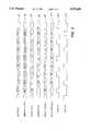
- FIG. 4illustrates the timing used to write data into the memory bank 16 or 18 which is currently receiving data via switch 14.
- the write strobe 88is provided at one-half the rate of the system clock 80.
- System clock 80runs at a rate of 2 ⁇ , which is the same as the read strobe.
- a separate write address from a stream of write addresses 82is provided during each write cycle for directing the two pixels present at the output of latch 12 into the next memory location of the receiving memory bank.
- Streams 84 and 86illustrate that two pixels are written into each memory location during each write cycle.
- pixels ⁇ 0 and ⁇ 1are input at the memory location designated by address ADR0.
- pixels ⁇ 2, ⁇ 3are stored at the memory location designated by ADR1.
- pixels ⁇ 4, ⁇ 5are stored at the memory location designated by ADR2.
- Stream 84is the data as input to terminal 10
- stream 86is the data after delayed by one clock cycle by latch 12. It is clear from FIG. 4 that during each write strobe 88, two pixels are available for writing into the memory location designated by the current address 82.
- switches 14 and 20are toggled so that the data can be read out of the memory bank while the next frame of data is written into the other memory bank.
- a separate addressis provided for each clock cycle during the read operation, as designated by 90 in FIG. 5.
- the first data streamwill provide data in the necessary order for DCT processing
- the second data streamwill provide data for processing in accordance with a film processing mode (FM).
- every other address 90provides data ordered for either DCT processing or film mode processing.
- the memory that is currently outputting datawill output pixels ⁇ 0, ⁇ 1 as illustrated at 90, 92 of FIG. 5.
- read address FM0will address the memory bank that is currently outputting data.
- the memory bankwill output pixels ⁇ 0, ⁇ 1 of the currently stored video frame.
- address DCT1will be provided to the memory bank, which will respond by outputting pixels ⁇ 2, ⁇ 3.
- address FM1will be provided to the memory bank, which will output pixels ⁇ 2, ⁇ 3 in response. The process will continue, so that every other read strobe, either a pair of DCT pixels or a pair of film mode pixels will be output from the memory bank.
- Register 22will be enabled by the ENA_A signal to latch only the DCT ordered pixels which are output in response to the DCT addresses. This is illustrated at 94.
- register 24will be responsive to the ENA_B signal to latch only the pixels output from the memory bank in the film mode order in response to the film mode addresses. This is illustrated at 96 in FIG. 5.
- the ENA_A and ENA_B signalsare illustrated at 102, 104, respectively, of FIG. 5.
- register 22Since register 22 will store only the pixels in the order output for DCT processing, the toggling of data selector 26 at the read strobe rate 2 ⁇ will provide Data Stream 1 at output terminal 27 containing the consecutive pixels ⁇ 0, ⁇ 1, ⁇ 2, ⁇ 3. . . as illustrated at 98. In the same manner, data selector 28 will output Data Stream 2 at terminal 29, comprising the pixels in the order ⁇ 0, ⁇ 1, ⁇ 2, ⁇ 3, ⁇ 4. . . as illustrated at 100.
- the present inventionprovides the capability of reading the data out in two different streams.
- the order of the data in each streamis controlled solely by the addresses provided to the outputting memory bank by the first read address generator 70 and second read address generator 72 illustrated in FIG. 3. These read address generators provide the address stream 90 illustrated in FIG. 5.
- FIG. 6illustrates an alternate embodiment of the present invention, in which separate registers are provided for each of the first and second memory banks 16, 18, respectively.
- first memory bank 16is associated with registers 30, 32 and second memory bank 18 is associated with registers 34, 36.
- the operation of registers 30, 32 and 34, 36is the same as the operation of registers 22, 24 in the embodiment of FIG. 1.
- Each registeris provided with either the ENA_A or ENA_B signal as well as the read strobe at the rate of 2 ⁇ .
- Each registerhas a data selector 40, 42, 44, or 46 associated with it in order to serialize the 16-bit pixel pairs into consecutive eight-bit pixels.
- Switches 48, 50each responsive to the next frame signal from the control processor 60 (FIG. 2) output the respective data streams from the memory bank currently outputting data.
- first memory bank 16when first memory bank 16 is outputting data, the pixels ordered in the appropriate order for Data Stream 1 will be output via terminal 52 from switch 48.
- second memory bankWhen the second memory bank is outputting data, the pixels in the order for Data Stream 1 will continue to be output on terminal 52 via switch 48.
- switch 50will output the pixels from first memory bank 16 in the order of Data Stream 2 via terminal 54.
- switch 50When the second memory bank is outputting data, switch 50 will couple the appropriately ordered pixels to terminal 54.
- the present inventionprocesses successive frames of pixel data to provide N data streams containing the pixel data in different orders.
- Incoming frames of pixel dataare alternately stored in a first memory bank at a rate of N pixels per write cycle while pixel data of a previous frame is output from a second memory bank at a rate of N pixels per read cycle.
- the read cyclehas a rate of N times the write cycle to provide N, N-pixel sets of output pixels per write cycle.
- the pixels output from the memory banks for each of the N setsare buffered to provide the N data streams in the appropriate orders.
- any number of data streamscan be provided by increasing the number of bytes stored in each memory location and providing a corresponding increase in the rate of the read strobe with respect to the write strobe.
Landscapes
- Engineering & Computer Science (AREA)
- Multimedia (AREA)
- Signal Processing (AREA)
- Compression Or Coding Systems Of Tv Signals (AREA)
- Communication Control (AREA)
- Image Input (AREA)
- Dram (AREA)
- Memory System (AREA)
- Data Exchanges In Wide-Area Networks (AREA)
- Small-Scale Networks (AREA)
- Television Systems (AREA)
- Controls And Circuits For Display Device (AREA)
- Time-Division Multiplex Systems (AREA)
Abstract
Description
Claims (19)
Priority Applications (10)
| Application Number | Priority Date | Filing Date | Title |
|---|---|---|---|
| US08/047,541US5572691A (en) | 1993-04-21 | 1993-04-21 | Apparatus and method for providing multiple data streams from stored data using dual memory buffers |
| TW087201731UTW385129U (en) | 1993-04-21 | 1993-04-30 | Dual memory buffer scheme for providing multiple data streams from stored data |
| AT94105690TATE188079T1 (en) | 1993-04-21 | 1994-04-13 | DOUBLE BUFFER SCHEME FOR PROCESSING MULTIPLE DATA STREAMS FROM STORED DATA |
| EP94105690AEP0621730B1 (en) | 1993-04-21 | 1994-04-13 | Dual memory buffer scheme for providing multiple data streams from stored data |
| CA002121196ACA2121196C (en) | 1993-04-21 | 1994-04-13 | Dual memory buffer scheme for providing multiple data streams from stored data |
| DE69422214TDE69422214T2 (en) | 1993-04-21 | 1994-04-13 | Double buffer scheme for the preparation of several data streams from stored data |
| AU60515/94AAU676012B2 (en) | 1993-04-21 | 1994-04-18 | Dual memory buffer scheme for providing multiple data streams from stored data |
| NO941430ANO941430L (en) | 1993-04-21 | 1994-04-20 | Dual memory buffer system for providing multiple data streams from stored data |
| JP10594194AJP3577103B2 (en) | 1993-04-21 | 1994-04-21 | Dual memory buffer apparatus and method for obtaining multiple data streams from stored data |
| KR1019940008419AKR100214100B1 (en) | 1993-04-21 | 1994-04-21 | Dual memory buffer structure for supplying multiple data streams from stored data |
Applications Claiming Priority (1)
| Application Number | Priority Date | Filing Date | Title |
|---|---|---|---|
| US08/047,541US5572691A (en) | 1993-04-21 | 1993-04-21 | Apparatus and method for providing multiple data streams from stored data using dual memory buffers |
Publications (1)
| Publication Number | Publication Date |
|---|---|
| US5572691Atrue US5572691A (en) | 1996-11-05 |
Family
ID=21949570
Family Applications (1)
| Application Number | Title | Priority Date | Filing Date |
|---|---|---|---|
| US08/047,541Expired - LifetimeUS5572691A (en) | 1993-04-21 | 1993-04-21 | Apparatus and method for providing multiple data streams from stored data using dual memory buffers |
Country Status (10)
| Country | Link |
|---|---|
| US (1) | US5572691A (en) |
| EP (1) | EP0621730B1 (en) |
| JP (1) | JP3577103B2 (en) |
| KR (1) | KR100214100B1 (en) |
| AT (1) | ATE188079T1 (en) |
| AU (1) | AU676012B2 (en) |
| CA (1) | CA2121196C (en) |
| DE (1) | DE69422214T2 (en) |
| NO (1) | NO941430L (en) |
| TW (1) | TW385129U (en) |
Cited By (51)
| Publication number | Priority date | Publication date | Assignee | Title |
|---|---|---|---|---|
| GB2311434A (en)* | 1996-03-21 | 1997-09-24 | Mitsubishi Electric Corp | Image decompressing apparatus with efficient image data storage |
| US5724537A (en) | 1994-03-24 | 1998-03-03 | Discovision Associates | Interface for connecting a bus to a random access memory using a two wire link |
| US5768624A (en)* | 1996-02-28 | 1998-06-16 | Opti Inc. | Method and apparatus for employing ping-pong buffering with one level deep buffers for fast DRAM access |
| US5802589A (en)* | 1995-09-28 | 1998-09-01 | Agfa Division, Bayer Corporation | Data buffering apparatus for buffering imaging data between a raster image processor (RIP) and an output device |
| US5829007A (en) | 1993-06-24 | 1998-10-27 | Discovision Associates | Technique for implementing a swing buffer in a memory array |
| US5835740A (en) | 1992-06-30 | 1998-11-10 | Discovision Associates | Data pipeline system and data encoding method |
| US5861894A (en) | 1993-06-24 | 1999-01-19 | Discovision Associates | Buffer manager |
| US5883610A (en)* | 1995-12-15 | 1999-03-16 | Samsung Electronics Co., Ltd. | Graphics overlay device |
| US5898442A (en)* | 1994-09-02 | 1999-04-27 | Kabushiki Kaisha Komatsu Seisakusho | Display control device |
| US5937177A (en)* | 1996-10-01 | 1999-08-10 | Sun Microsystems, Inc. | Control structure for a high-speed asynchronous pipeline |
| US5943504A (en)* | 1997-04-14 | 1999-08-24 | International Business Machines Corporation | System for transferring pixel data from a digitizer to a host memory using scatter/gather DMA |
| US5982674A (en)* | 1997-09-30 | 1999-11-09 | Mosaid Technologies Incorporated | Bi-directional data bus scheme with optimized read and write characters |
| US6003096A (en)* | 1996-10-17 | 1999-12-14 | Samsung Electronics Co., Ltd. | Host interface circuit for preventing data loss and improving interface speed for an image forming apparatus by latching received data in response to a strobe input signal |
| US6018354A (en) | 1994-03-24 | 2000-01-25 | Discovision Associates | Method for accessing banks of DRAM |
| US6034674A (en)* | 1992-06-30 | 2000-03-07 | Discovision Associates | Buffer manager |
| US6073203A (en)* | 1996-12-11 | 2000-06-06 | Rohde & Schwarz Gmbh & Co. Kg | Method for the continuous readout of a data sequence from a memory |
| US6081877A (en)* | 1996-02-29 | 2000-06-27 | Fujitsu Limited | Method and apparatus for fast data transfer using internal clock of relatively low frequency |
| US6111595A (en)* | 1997-08-22 | 2000-08-29 | Northern Information Technology | Rapid update video link |
| US6122315A (en)* | 1997-02-26 | 2000-09-19 | Discovision Associates | Memory manager for MPEG decoder |
| US6131151A (en)* | 1997-11-12 | 2000-10-10 | Lsi Logic Corporation | Processing high-speed digital datastreams with reduced memory |
| US6185640B1 (en)* | 1998-06-19 | 2001-02-06 | Philips Electronics North America Corporation | Minimal frame buffer manager allowing simultaneous read/write access by alternately filling and emptying a first and second buffer one packet at a time |
| US6253303B1 (en)* | 1996-08-09 | 2001-06-26 | Nec Corporation | Audio signal processing circuit |
| US6295295B1 (en)* | 1995-11-27 | 2001-09-25 | Telefonaktiebolaget Lm Ericsson | Scheduler for an information packet switch |
| US6300964B1 (en)* | 1998-07-30 | 2001-10-09 | Genesis Microship, Inc. | Method and apparatus for storage retrieval of digital image data |
| US6326999B1 (en)* | 1994-08-23 | 2001-12-04 | Discovision Associates | Data rate conversion |
| US6364770B1 (en)* | 1998-10-08 | 2002-04-02 | Konami Co., Ltd. | Image creating apparatus, displayed scene switching method for the image creating apparatus, computer-readable recording medium containing displayed scene switching program for the image creating apparatus, and video game machine |
| US20020070943A1 (en)* | 2000-09-07 | 2002-06-13 | Hall Deirdre M. | Graphics memory system for volumeric displays |
| US6553450B1 (en)* | 2000-09-18 | 2003-04-22 | Intel Corporation | Buffer to multiply memory interface |
| US20030131191A1 (en)* | 2001-11-26 | 2003-07-10 | Broadlogic Network Technologies, Inc. | Multi-stream access scheme for high speed access and recording using a hard disk drive |
| US6697888B1 (en) | 2000-09-29 | 2004-02-24 | Intel Corporation | Buffering and interleaving data transfer between a chipset and memory modules |
| US20040057269A1 (en)* | 2002-03-07 | 2004-03-25 | Bhakta Jayesh R. | Arrangement of integrated circuits in a memory module |
| US20040090404A1 (en)* | 2002-10-21 | 2004-05-13 | Masami Endo | Display device and driving method thereof |
| US20040123056A1 (en)* | 2002-12-23 | 2004-06-24 | Intel Corporation | Interleaving memory access |
| US6820163B1 (en) | 2000-09-18 | 2004-11-16 | Intel Corporation | Buffering data transfer between a chipset and memory modules |
| US20040227764A1 (en)* | 2003-05-16 | 2004-11-18 | Semiconductor Energy Laboratory Co., Ltd. | Display device, method for driving the same, and electronic device using the same |
| US20050018495A1 (en)* | 2004-01-29 | 2005-01-27 | Netlist, Inc. | Arrangement of integrated circuits in a memory module |
| US20050050259A1 (en)* | 2003-09-02 | 2005-03-03 | Tim Niggemeier | Method for multibank memory scheduling |
| US20050169278A1 (en)* | 2002-04-12 | 2005-08-04 | Xyratex Technology Limited | Atm traffic generator with interleave memory |
| US20060008180A1 (en)* | 2004-06-23 | 2006-01-12 | Wakeland Carl K | Method and device to process digital media streams |
| US20060170708A1 (en)* | 2005-02-02 | 2006-08-03 | Samsung Electronics Co., Ltd. | Circuits for processing encoded image data using reduced external memory access and methods of operating the same |
| US20070083733A1 (en)* | 2004-07-30 | 2007-04-12 | Fujitsu Limited | Reconfigurable circuit and control method therefor |
| US20080005417A1 (en)* | 2006-06-16 | 2008-01-03 | Mtekvision Co., Ltd. | Method for speedy delivery of data between processors and digital processing apparatus having shared memory |
| US20120127367A1 (en)* | 2010-11-24 | 2012-05-24 | Ati Technologies Ulc | Method and apparatus for providing temporal image processing using multi-stream field information |
| US8516188B1 (en) | 2004-03-05 | 2013-08-20 | Netlist, Inc. | Circuit for memory module |
| US8756364B1 (en) | 2004-03-05 | 2014-06-17 | Netlist, Inc. | Multirank DDR memory modual with load reduction |
| US8782350B2 (en) | 2008-04-14 | 2014-07-15 | Netlist, Inc. | Circuit providing load isolation and noise reduction |
| US9128632B2 (en) | 2009-07-16 | 2015-09-08 | Netlist, Inc. | Memory module with distributed data buffers and method of operation |
| US9606907B2 (en) | 2009-07-16 | 2017-03-28 | Netlist, Inc. | Memory module with distributed data buffers and method of operation |
| US10290328B2 (en) | 2010-11-03 | 2019-05-14 | Netlist, Inc. | Memory module with packages of stacked memory chips |
| US10324841B2 (en) | 2013-07-27 | 2019-06-18 | Netlist, Inc. | Memory module with local synchronization |
| US10755757B2 (en) | 2004-01-05 | 2020-08-25 | Smart Modular Technologies, Inc. | Multi-rank memory module that emulates a memory module having a different number of ranks |
Families Citing this family (8)
| Publication number | Priority date | Publication date | Assignee | Title |
|---|---|---|---|---|
| KR100198541B1 (en)* | 1996-08-26 | 1999-06-15 | 구자홍 | Method for storing image frame data in memory |
| US6078958A (en)* | 1997-01-31 | 2000-06-20 | Hughes Electronics Corporation | System for allocating available bandwidth of a concentrated media output |
| US6097435A (en)* | 1997-01-31 | 2000-08-01 | Hughes Electronics Corporation | Video system with selectable bit rate reduction |
| US6188436B1 (en) | 1997-01-31 | 2001-02-13 | Hughes Electronics Corporation | Video broadcast system with video data shifting |
| US6084910A (en)* | 1997-01-31 | 2000-07-04 | Hughes Electronics Corporation | Statistical multiplexer for video signals |
| US6005620A (en)* | 1997-01-31 | 1999-12-21 | Hughes Electronics Corporation | Statistical multiplexer for live and pre-compressed video |
| US6091455A (en)* | 1997-01-31 | 2000-07-18 | Hughes Electronics Corporation | Statistical multiplexer for recording video |
| JP4753709B2 (en)* | 2005-12-21 | 2011-08-24 | 三洋電機株式会社 | Data multiplexing storage device and processing device |
Citations (20)
| Publication number | Priority date | Publication date | Assignee | Title |
|---|---|---|---|---|
| US4352180A (en)* | 1979-04-27 | 1982-09-28 | Elmar Schulze | Digital time-division multiplex telecommunication system |
| US4394642A (en)* | 1981-09-21 | 1983-07-19 | Sperry Corporation | Apparatus for interleaving and de-interleaving data |
| US4472813A (en)* | 1981-03-30 | 1984-09-18 | Nippon Electric Co., Ltd. | Transmission system for intentionally violating a class IV partial response code to distinguish subsidiary signals from an error |
| US4674088A (en)* | 1985-03-07 | 1987-06-16 | Northern Telecom Limited | Method and apparatus for detecting frame synchronization |
| US4728930A (en)* | 1987-06-30 | 1988-03-01 | The United States Of America As Represented By The Secretary Of The Navy | Parallel-to-serial-data interface-adaptor |
| US4791598A (en)* | 1987-03-24 | 1988-12-13 | Bell Communications Research, Inc. | Two-dimensional discrete cosine transform processor |
| US4807121A (en)* | 1984-06-21 | 1989-02-21 | Cray Research, Inc. | Peripheral interface system |
| US4956768A (en)* | 1987-02-25 | 1990-09-11 | Etat Francais, Centre National d'Etudes des Telecommunications | Wideband server, in particular for transmitting music or images |
| US5007001A (en)* | 1990-01-24 | 1991-04-09 | Lloyd Williams Andrew | Method for reordering the pixel map of a digitized image |
| US5138440A (en)* | 1990-10-29 | 1992-08-11 | General Instrument Corporation | Method and apparatus for communicating a plurality of asynchronous signals over a digital communication path |
| US5163132A (en)* | 1987-09-24 | 1992-11-10 | Ncr Corporation | Integrated controller using alternately filled and emptied buffers for controlling bi-directional data transfer between a processor and a data storage device |
| US5195182A (en)* | 1989-04-03 | 1993-03-16 | Eastman Kodak Company | Frame buffer architecture for storing sequential data in alternating memory banks |
| US5197145A (en)* | 1988-09-20 | 1993-03-23 | Fujitsu Limited | Buffer storage system using parallel buffer storage units and move-out buffer registers |
| US5229855A (en)* | 1991-07-18 | 1993-07-20 | International Business Machines Corporation | System and method for combining multiple composite video signals |
| US5249292A (en)* | 1989-03-31 | 1993-09-28 | Chiappa J Noel | Data packet switch using a primary processing unit to designate one of a plurality of data stream control circuits to selectively handle the header processing of incoming packets in one data packet stream |
| US5261068A (en)* | 1990-05-25 | 1993-11-09 | Dell Usa L.P. | Dual path memory retrieval system for an interleaved dynamic RAM memory unit |
| US5297139A (en)* | 1991-06-19 | 1994-03-22 | Hitachi, Ltd. | Data communication system |
| US5307449A (en)* | 1991-12-20 | 1994-04-26 | Apple Computer, Inc. | Method and apparatus for simultaneously rendering multiple scanlines |
| US5371877A (en)* | 1991-12-31 | 1994-12-06 | Apple Computer, Inc. | Apparatus for alternatively accessing single port random access memories to implement dual port first-in first-out memory |
| US5377265A (en)* | 1992-01-31 | 1994-12-27 | Alcatel N.V. | Parallel additive scrambler and descrambler |
- 1993
- 1993-04-21USUS08/047,541patent/US5572691A/ennot_activeExpired - Lifetime
- 1993-04-30TWTW087201731Upatent/TW385129U/ennot_activeIP Right Cessation
- 1994
- 1994-04-13EPEP94105690Apatent/EP0621730B1/ennot_activeExpired - Lifetime
- 1994-04-13ATAT94105690Tpatent/ATE188079T1/enactive
- 1994-04-13CACA002121196Apatent/CA2121196C/ennot_activeExpired - Lifetime
- 1994-04-13DEDE69422214Tpatent/DE69422214T2/ennot_activeExpired - Lifetime
- 1994-04-18AUAU60515/94Apatent/AU676012B2/ennot_activeCeased
- 1994-04-20NONO941430Apatent/NO941430L/enunknown
- 1994-04-21JPJP10594194Apatent/JP3577103B2/ennot_activeExpired - Lifetime
- 1994-04-21KRKR1019940008419Apatent/KR100214100B1/ennot_activeExpired - Fee Related
Patent Citations (20)
| Publication number | Priority date | Publication date | Assignee | Title |
|---|---|---|---|---|
| US4352180A (en)* | 1979-04-27 | 1982-09-28 | Elmar Schulze | Digital time-division multiplex telecommunication system |
| US4472813A (en)* | 1981-03-30 | 1984-09-18 | Nippon Electric Co., Ltd. | Transmission system for intentionally violating a class IV partial response code to distinguish subsidiary signals from an error |
| US4394642A (en)* | 1981-09-21 | 1983-07-19 | Sperry Corporation | Apparatus for interleaving and de-interleaving data |
| US4807121A (en)* | 1984-06-21 | 1989-02-21 | Cray Research, Inc. | Peripheral interface system |
| US4674088A (en)* | 1985-03-07 | 1987-06-16 | Northern Telecom Limited | Method and apparatus for detecting frame synchronization |
| US4956768A (en)* | 1987-02-25 | 1990-09-11 | Etat Francais, Centre National d'Etudes des Telecommunications | Wideband server, in particular for transmitting music or images |
| US4791598A (en)* | 1987-03-24 | 1988-12-13 | Bell Communications Research, Inc. | Two-dimensional discrete cosine transform processor |
| US4728930A (en)* | 1987-06-30 | 1988-03-01 | The United States Of America As Represented By The Secretary Of The Navy | Parallel-to-serial-data interface-adaptor |
| US5163132A (en)* | 1987-09-24 | 1992-11-10 | Ncr Corporation | Integrated controller using alternately filled and emptied buffers for controlling bi-directional data transfer between a processor and a data storage device |
| US5197145A (en)* | 1988-09-20 | 1993-03-23 | Fujitsu Limited | Buffer storage system using parallel buffer storage units and move-out buffer registers |
| US5249292A (en)* | 1989-03-31 | 1993-09-28 | Chiappa J Noel | Data packet switch using a primary processing unit to designate one of a plurality of data stream control circuits to selectively handle the header processing of incoming packets in one data packet stream |
| US5195182A (en)* | 1989-04-03 | 1993-03-16 | Eastman Kodak Company | Frame buffer architecture for storing sequential data in alternating memory banks |
| US5007001A (en)* | 1990-01-24 | 1991-04-09 | Lloyd Williams Andrew | Method for reordering the pixel map of a digitized image |
| US5261068A (en)* | 1990-05-25 | 1993-11-09 | Dell Usa L.P. | Dual path memory retrieval system for an interleaved dynamic RAM memory unit |
| US5138440A (en)* | 1990-10-29 | 1992-08-11 | General Instrument Corporation | Method and apparatus for communicating a plurality of asynchronous signals over a digital communication path |
| US5297139A (en)* | 1991-06-19 | 1994-03-22 | Hitachi, Ltd. | Data communication system |
| US5229855A (en)* | 1991-07-18 | 1993-07-20 | International Business Machines Corporation | System and method for combining multiple composite video signals |
| US5307449A (en)* | 1991-12-20 | 1994-04-26 | Apple Computer, Inc. | Method and apparatus for simultaneously rendering multiple scanlines |
| US5371877A (en)* | 1991-12-31 | 1994-12-06 | Apple Computer, Inc. | Apparatus for alternatively accessing single port random access memories to implement dual port first-in first-out memory |
| US5377265A (en)* | 1992-01-31 | 1994-12-27 | Alcatel N.V. | Parallel additive scrambler and descrambler |
Non-Patent Citations (2)
| Title |
|---|
| D. T. Chi, "A New Block Helical Interleaver," Conference Record of MILCOM '92; Oct. 11-14, 1992, San Diego, CA, vol. 2/3, pp. 799-804. |
| D. T. Chi, A New Block Helical Interleaver, Conference Record of MILCOM 92; Oct. 11 14, 1992, San Diego, CA, vol. 2/3, pp. 799 804.* |
Cited By (88)
| Publication number | Priority date | Publication date | Assignee | Title |
|---|---|---|---|---|
| US6034674A (en)* | 1992-06-30 | 2000-03-07 | Discovision Associates | Buffer manager |
| US5835740A (en) | 1992-06-30 | 1998-11-10 | Discovision Associates | Data pipeline system and data encoding method |
| US5835792A (en) | 1993-06-24 | 1998-11-10 | Discovision Associates | Token-based adaptive video processing arrangement |
| US5861894A (en) | 1993-06-24 | 1999-01-19 | Discovision Associates | Buffer manager |
| US5829007A (en) | 1993-06-24 | 1998-10-27 | Discovision Associates | Technique for implementing a swing buffer in a memory array |
| US6018354A (en) | 1994-03-24 | 2000-01-25 | Discovision Associates | Method for accessing banks of DRAM |
| US5956741A (en) | 1994-03-24 | 1999-09-21 | Discovision Associates | Interface for connecting a bus to a random access memory using a swing buffer and a buffer manager |
| US5724537A (en) | 1994-03-24 | 1998-03-03 | Discovision Associates | Interface for connecting a bus to a random access memory using a two wire link |
| US5984512A (en) | 1994-07-29 | 1999-11-16 | Discovision Associates | Method for storing video information |
| US6326999B1 (en)* | 1994-08-23 | 2001-12-04 | Discovision Associates | Data rate conversion |
| US5898442A (en)* | 1994-09-02 | 1999-04-27 | Kabushiki Kaisha Komatsu Seisakusho | Display control device |
| US5802589A (en)* | 1995-09-28 | 1998-09-01 | Agfa Division, Bayer Corporation | Data buffering apparatus for buffering imaging data between a raster image processor (RIP) and an output device |
| US6295295B1 (en)* | 1995-11-27 | 2001-09-25 | Telefonaktiebolaget Lm Ericsson | Scheduler for an information packet switch |
| US5883610A (en)* | 1995-12-15 | 1999-03-16 | Samsung Electronics Co., Ltd. | Graphics overlay device |
| US5768624A (en)* | 1996-02-28 | 1998-06-16 | Opti Inc. | Method and apparatus for employing ping-pong buffering with one level deep buffers for fast DRAM access |
| US6081877A (en)* | 1996-02-29 | 2000-06-27 | Fujitsu Limited | Method and apparatus for fast data transfer using internal clock of relatively low frequency |
| GB2311434B (en)* | 1996-03-21 | 2000-01-12 | Mitsubishi Electric Corp | Image decompressing apparatus with efficient image data transfer |
| US5850483A (en)* | 1996-03-21 | 1998-12-15 | Mitsubishi Denki Kabushiki Kaisha | Image decompressing apparatus with efficient image data transfer |
| GB2311434A (en)* | 1996-03-21 | 1997-09-24 | Mitsubishi Electric Corp | Image decompressing apparatus with efficient image data storage |
| US6253303B1 (en)* | 1996-08-09 | 2001-06-26 | Nec Corporation | Audio signal processing circuit |
| US5937177A (en)* | 1996-10-01 | 1999-08-10 | Sun Microsystems, Inc. | Control structure for a high-speed asynchronous pipeline |
| US6003096A (en)* | 1996-10-17 | 1999-12-14 | Samsung Electronics Co., Ltd. | Host interface circuit for preventing data loss and improving interface speed for an image forming apparatus by latching received data in response to a strobe input signal |
| US6073203A (en)* | 1996-12-11 | 2000-06-06 | Rohde & Schwarz Gmbh & Co. Kg | Method for the continuous readout of a data sequence from a memory |
| US6122315A (en)* | 1997-02-26 | 2000-09-19 | Discovision Associates | Memory manager for MPEG decoder |
| US5943504A (en)* | 1997-04-14 | 1999-08-24 | International Business Machines Corporation | System for transferring pixel data from a digitizer to a host memory using scatter/gather DMA |
| US6111595A (en)* | 1997-08-22 | 2000-08-29 | Northern Information Technology | Rapid update video link |
| US5982674A (en)* | 1997-09-30 | 1999-11-09 | Mosaid Technologies Incorporated | Bi-directional data bus scheme with optimized read and write characters |
| US6131151A (en)* | 1997-11-12 | 2000-10-10 | Lsi Logic Corporation | Processing high-speed digital datastreams with reduced memory |
| US6185640B1 (en)* | 1998-06-19 | 2001-02-06 | Philips Electronics North America Corporation | Minimal frame buffer manager allowing simultaneous read/write access by alternately filling and emptying a first and second buffer one packet at a time |
| US6300964B1 (en)* | 1998-07-30 | 2001-10-09 | Genesis Microship, Inc. | Method and apparatus for storage retrieval of digital image data |
| US6364770B1 (en)* | 1998-10-08 | 2002-04-02 | Konami Co., Ltd. | Image creating apparatus, displayed scene switching method for the image creating apparatus, computer-readable recording medium containing displayed scene switching program for the image creating apparatus, and video game machine |
| US20020070943A1 (en)* | 2000-09-07 | 2002-06-13 | Hall Deirdre M. | Graphics memory system for volumeric displays |
| US6873335B2 (en)* | 2000-09-07 | 2005-03-29 | Actuality Systems, Inc. | Graphics memory system for volumeric displays |
| US6553450B1 (en)* | 2000-09-18 | 2003-04-22 | Intel Corporation | Buffer to multiply memory interface |
| US6820163B1 (en) | 2000-09-18 | 2004-11-16 | Intel Corporation | Buffering data transfer between a chipset and memory modules |
| US6697888B1 (en) | 2000-09-29 | 2004-02-24 | Intel Corporation | Buffering and interleaving data transfer between a chipset and memory modules |
| US7249232B2 (en) | 2000-09-29 | 2007-07-24 | Intel Corporation | Buffering and interleaving data transfer between a chipset and memory modules |
| US20040188704A1 (en)* | 2000-09-29 | 2004-09-30 | Intel Corporation, A Delaware Corporation | Buffering and interleaving data transfer between a chipset and memory modules |
| US20030131191A1 (en)* | 2001-11-26 | 2003-07-10 | Broadlogic Network Technologies, Inc. | Multi-stream access scheme for high speed access and recording using a hard disk drive |
| US7647459B2 (en)* | 2001-11-26 | 2010-01-12 | Broadlogic Network Technologies, Inc. | Multi-stream access scheme for high speed access and recording using a hard disk drive |
| US20040184300A1 (en)* | 2002-03-07 | 2004-09-23 | Bhakta Jayesh R. | Arrangement of integrated circuits in a memory module |
| US6930903B2 (en) | 2002-03-07 | 2005-08-16 | Netlist, Inc. | Arrangement of integrated circuits in a memory module |
| US20040184301A1 (en)* | 2002-03-07 | 2004-09-23 | Bhakta Jayesh R. | Arrangement of integrated circuits in a memory module |
| US20040136229A1 (en)* | 2002-03-07 | 2004-07-15 | Bhakta Jayesh R. | Arrangement of integrated circuits in a memory module |
| US6930900B2 (en) | 2002-03-07 | 2005-08-16 | Netlist, Inc. | Arrangement of integrated circuits in a memory module |
| US20040184299A1 (en)* | 2002-03-07 | 2004-09-23 | Bhakta Jayesh R. | Arrangement of integrated circuits in a memory module |
| US6873534B2 (en) | 2002-03-07 | 2005-03-29 | Netlist, Inc. | Arrangement of integrated circuits in a memory module |
| US20040057269A1 (en)* | 2002-03-07 | 2004-03-25 | Bhakta Jayesh R. | Arrangement of integrated circuits in a memory module |
| US20050169278A1 (en)* | 2002-04-12 | 2005-08-04 | Xyratex Technology Limited | Atm traffic generator with interleave memory |
| US20080174579A1 (en)* | 2002-10-21 | 2008-07-24 | Semiconductor Energy Laboratory Co., Ltd. | Display device and driving method thereof |
| US20040090404A1 (en)* | 2002-10-21 | 2004-05-13 | Masami Endo | Display device and driving method thereof |
| US7330179B2 (en)* | 2002-10-21 | 2008-02-12 | Semiconductor Energy Laboratory Co., Ltd. | Display device and driving method thereof |
| US20040123056A1 (en)* | 2002-12-23 | 2004-06-24 | Intel Corporation | Interleaving memory access |
| US6944728B2 (en)* | 2002-12-23 | 2005-09-13 | Intel Corporation | Interleaving memory access |
| US20040227764A1 (en)* | 2003-05-16 | 2004-11-18 | Semiconductor Energy Laboratory Co., Ltd. | Display device, method for driving the same, and electronic device using the same |
| CN100430983C (en)* | 2003-05-16 | 2008-11-05 | 株式会社半导体能源研究所 | Display device, method for driving the same, and electronic device using the same |
| US7551166B2 (en) | 2003-05-16 | 2009-06-23 | Semiconductor Energy Laboratory Co., Ltd. | Display device, method for driving the same, and electronic device using the same |
| US7613866B2 (en)* | 2003-09-02 | 2009-11-03 | Thomson Licensing | Method for controlling access to a multibank memory |
| US20050050259A1 (en)* | 2003-09-02 | 2005-03-03 | Tim Niggemeier | Method for multibank memory scheduling |
| US10755757B2 (en) | 2004-01-05 | 2020-08-25 | Smart Modular Technologies, Inc. | Multi-rank memory module that emulates a memory module having a different number of ranks |
| US20050018495A1 (en)* | 2004-01-29 | 2005-01-27 | Netlist, Inc. | Arrangement of integrated circuits in a memory module |
| US10489314B2 (en) | 2004-03-05 | 2019-11-26 | Netlist, Inc. | Memory module with data buffering |
| US9858215B1 (en) | 2004-03-05 | 2018-01-02 | Netlist, Inc. | Memory module with data buffering |
| US12222878B2 (en) | 2004-03-05 | 2025-02-11 | Netlist, Inc. | Memory module with data buffering |
| US11093417B2 (en) | 2004-03-05 | 2021-08-17 | Netlist, Inc. | Memory module with data buffering |
| US8756364B1 (en) | 2004-03-05 | 2014-06-17 | Netlist, Inc. | Multirank DDR memory modual with load reduction |
| US8516188B1 (en) | 2004-03-05 | 2013-08-20 | Netlist, Inc. | Circuit for memory module |
| US7457484B2 (en) | 2004-06-23 | 2008-11-25 | Creative Technology Ltd | Method and device to process digital media streams |
| US20060008180A1 (en)* | 2004-06-23 | 2006-01-12 | Wakeland Carl K | Method and device to process digital media streams |
| WO2006002209A3 (en)* | 2004-06-23 | 2007-02-22 | Creative Tech Ltd | Processing digital media streams |
| US7849288B2 (en)* | 2004-07-30 | 2010-12-07 | Fujitsu Limited | Alternately selecting memory units to store and retrieve configuration information in respective areas for a plurality of processing elements to perform pipelined processes |
| US20070083733A1 (en)* | 2004-07-30 | 2007-04-12 | Fujitsu Limited | Reconfigurable circuit and control method therefor |
| US20060170708A1 (en)* | 2005-02-02 | 2006-08-03 | Samsung Electronics Co., Ltd. | Circuits for processing encoded image data using reduced external memory access and methods of operating the same |
| US20080005417A1 (en)* | 2006-06-16 | 2008-01-03 | Mtekvision Co., Ltd. | Method for speedy delivery of data between processors and digital processing apparatus having shared memory |
| US9037809B1 (en) | 2008-04-14 | 2015-05-19 | Netlist, Inc. | Memory module with circuit providing load isolation and noise reduction |
| US8782350B2 (en) | 2008-04-14 | 2014-07-15 | Netlist, Inc. | Circuit providing load isolation and noise reduction |
| US9606907B2 (en) | 2009-07-16 | 2017-03-28 | Netlist, Inc. | Memory module with distributed data buffers and method of operation |
| US9128632B2 (en) | 2009-07-16 | 2015-09-08 | Netlist, Inc. | Memory module with distributed data buffers and method of operation |
| US11994982B2 (en) | 2009-07-16 | 2024-05-28 | Netlist, Inc. | Memory module with distributed data buffers |
| US10949339B2 (en) | 2009-07-16 | 2021-03-16 | Netlist, Inc. | Memory module with controlled byte-wise buffers |
| US10290328B2 (en) | 2010-11-03 | 2019-05-14 | Netlist, Inc. | Memory module with packages of stacked memory chips |
| US20120127367A1 (en)* | 2010-11-24 | 2012-05-24 | Ati Technologies Ulc | Method and apparatus for providing temporal image processing using multi-stream field information |
| US10424274B2 (en)* | 2010-11-24 | 2019-09-24 | Ati Technologies Ulc | Method and apparatus for providing temporal image processing using multi-stream field information |
| US10268608B2 (en) | 2012-07-27 | 2019-04-23 | Netlist, Inc. | Memory module with timing-controlled data paths in distributed data buffers |
| US10860506B2 (en) | 2012-07-27 | 2020-12-08 | Netlist, Inc. | Memory module with timing-controlled data buffering |
| US11762788B2 (en) | 2012-07-27 | 2023-09-19 | Netlist, Inc. | Memory module with timing-controlled data buffering |
| US10324841B2 (en) | 2013-07-27 | 2019-06-18 | Netlist, Inc. | Memory module with local synchronization |
| US10884923B2 (en) | 2013-07-27 | 2021-01-05 | Netlist, Inc. | Memory module with local synchronization and method of operation |
Also Published As
| Publication number | Publication date |
|---|---|
| EP0621730A2 (en) | 1994-10-26 |
| JPH0736773A (en) | 1995-02-07 |
| JP3577103B2 (en) | 2004-10-13 |
| EP0621730A3 (en) | 1995-07-26 |
| KR940025353A (en) | 1994-11-19 |
| AU6051594A (en) | 1994-10-27 |
| NO941430L (en) | 1994-10-24 |
| DE69422214D1 (en) | 2000-01-27 |
| KR100214100B1 (en) | 1999-08-02 |
| ATE188079T1 (en) | 2000-01-15 |
| CA2121196A1 (en) | 1994-10-22 |
| AU676012B2 (en) | 1997-02-27 |
| EP0621730B1 (en) | 1999-12-22 |
| NO941430D0 (en) | 1994-04-20 |
| DE69422214T2 (en) | 2000-09-07 |
| CA2121196C (en) | 1998-11-03 |
| TW385129U (en) | 2000-03-11 |
Similar Documents
| Publication | Publication Date | Title |
|---|---|---|
| US5572691A (en) | Apparatus and method for providing multiple data streams from stored data using dual memory buffers | |
| US6151075A (en) | Device and method for converting frame rate | |
| KR100188427B1 (en) | Variable length codeword decoder for digital communication system and decoding method thereof | |
| US5581310A (en) | Architecture for a high definition video frame memory and an accompanying data organization for use therewith and efficient access therefrom | |
| KR100246878B1 (en) | Inverse discrete cosine transform processor | |
| US5504823A (en) | Image data partitioning circuit for parallel image decoding system | |
| US4281344A (en) | Video interframe transform coding technique | |
| JPH08130745A (en) | Decoding system, decoding device, and decoding circuit | |
| US6020924A (en) | Reduced memory size set top box which stores frames and associated motion vectors which indicate which block or blocks are to be retrieved from memory | |
| GB2269289A (en) | Serial data decoding | |
| US5995171A (en) | Coding and/or decoding apparatus for decoding variable-length coded image information | |
| JP3224060B2 (en) | Decoder apparatus and method with two-stage buffer for variable length decoder | |
| JP3285220B2 (en) | Television system for transmitting image signals in digital form | |
| EP0566184A2 (en) | Picture transformer and television system with a transmitter and a receiver comprising a picture transformer | |
| US6233280B1 (en) | Video decoder for high picture quality | |
| JP3238571B2 (en) | Variable length decoding device | |
| JPH04326669A (en) | Image encoding device and image encoding method | |
| US5699120A (en) | Motion vector using a transform function identification signal | |
| JP2817409B2 (en) | Color image signal decoding device | |
| CN1126410A (en) | Apparatus for parallel decoding of digital video signals | |
| KR970002480B1 (en) | Motion compensation device applied to screen division structure | |
| JPS63227271A (en) | Hierarchical transmission method for still images | |
| JPH0646405A (en) | Image converter and television system, having transmitter and receiver, provided with it | |
| Grüger et al. | VLSI architectures of filterbanks for subband coding of HDTV signals | |
| JPH05347755A (en) | Video coding device |
Legal Events
| Date | Code | Title | Description |
|---|---|---|---|
| AS | Assignment | Owner name:GI CORPORATION, PENNSYLVANIA Free format text:ASSIGNMENT OF ASSIGNORS INTEREST.;ASSIGNOR:KOUDMANI, RABEE;REEL/FRAME:006511/0273 Effective date:19930416 | |
| STPP | Information on status: patent application and granting procedure in general | Free format text:APPLICATION UNDERGOING PREEXAM PROCESSING | |
| CC | Certificate of correction | ||
| AS | Assignment | Owner name:GENERAL INSTRUMENT CORPORATION, PENNSYLVANIA Free format text:ASSIGNMENT OF ASSIGNORS INTEREST;ASSIGNOR:GI CORPORATION;REEL/FRAME:009138/0551 Effective date:19980414 | |
| FEPP | Fee payment procedure | Free format text:PAYOR NUMBER ASSIGNED (ORIGINAL EVENT CODE: ASPN); ENTITY STATUS OF PATENT OWNER: LARGE ENTITY | |
| FPAY | Fee payment | Year of fee payment:4 | |
| FPAY | Fee payment | Year of fee payment:8 | |
| FPAY | Fee payment | Year of fee payment:12 | |
| AS | Assignment | Owner name:MOTOROLA MOBILITY LLC, ILLINOIS Free format text:ASSIGNMENT OF ASSIGNORS INTEREST;ASSIGNOR:GENERAL INSTRUMENT HOLDINGS, INC.;REEL/FRAME:030866/0113 Effective date:20130528 Owner name:GENERAL INSTRUMENT HOLDINGS, INC., CALIFORNIA Free format text:ASSIGNMENT OF ASSIGNORS INTEREST;ASSIGNOR:GENERAL INSTRUMENT CORPORATION;REEL/FRAME:030764/0575 Effective date:20130415 | |
| AS | Assignment | Owner name:GOOGLE TECHNOLOGY HOLDINGS LLC, CALIFORNIA Free format text:ASSIGNMENT OF ASSIGNORS INTEREST;ASSIGNOR:MOTOROLA MOBILITY LLC;REEL/FRAME:034491/0001 Effective date:20141028 |