US5572335A - Method and system for transferring image data between two devices having different bandwidths - Google Patents
Method and system for transferring image data between two devices having different bandwidthsDownload PDFInfo
- Publication number
- US5572335A US5572335AUS08/222,200US22220094AUS5572335AUS 5572335 AUS5572335 AUS 5572335AUS 22220094 AUS22220094 AUS 22220094AUS 5572335 AUS5572335 AUS 5572335A
- Authority
- US
- United States
- Prior art keywords
- image data
- scanlines
- valid
- data
- image
- Prior art date
- Legal status (The legal status is an assumption and is not a legal conclusion. Google has not performed a legal analysis and makes no representation as to the accuracy of the status listed.)
- Expired - Lifetime
Links
Images


Classifications
- H—ELECTRICITY
- H04—ELECTRIC COMMUNICATION TECHNIQUE
- H04N—PICTORIAL COMMUNICATION, e.g. TELEVISION
- H04N1/00—Scanning, transmission or reproduction of documents or the like, e.g. facsimile transmission; Details thereof
- H04N1/32—Circuits or arrangements for control or supervision between transmitter and receiver or between image input and image output device, e.g. between a still-image camera and its memory or between a still-image camera and a printer device
- H04N1/32358—Circuits or arrangements for control or supervision between transmitter and receiver or between image input and image output device, e.g. between a still-image camera and its memory or between a still-image camera and a printer device using picture signal storage, e.g. at transmitter
- H04N1/32491—Circuits or arrangements for control or supervision between transmitter and receiver or between image input and image output device, e.g. between a still-image camera and its memory or between a still-image camera and a printer device using picture signal storage, e.g. at transmitter alternate storage in and retrieval from two parallel memories, e.g. using ping-pong buffers
- H—ELECTRICITY
- H04—ELECTRIC COMMUNICATION TECHNIQUE
- H04N—PICTORIAL COMMUNICATION, e.g. TELEVISION
- H04N1/00—Scanning, transmission or reproduction of documents or the like, e.g. facsimile transmission; Details thereof
- H04N1/32—Circuits or arrangements for control or supervision between transmitter and receiver or between image input and image output device, e.g. between a still-image camera and its memory or between a still-image camera and a printer device
- H04N1/32358—Circuits or arrangements for control or supervision between transmitter and receiver or between image input and image output device, e.g. between a still-image camera and its memory or between a still-image camera and a printer device using picture signal storage, e.g. at transmitter
- H—ELECTRICITY
- H04—ELECTRIC COMMUNICATION TECHNIQUE
- H04N—PICTORIAL COMMUNICATION, e.g. TELEVISION
- H04N1/00—Scanning, transmission or reproduction of documents or the like, e.g. facsimile transmission; Details thereof
- H04N1/00127—Connection or combination of a still picture apparatus with another apparatus, e.g. for storage, processing or transmission of still picture signals or of information associated with a still picture
- H04N1/00204—Connection or combination of a still picture apparatus with another apparatus, e.g. for storage, processing or transmission of still picture signals or of information associated with a still picture with a digital computer or a digital computer system, e.g. an internet server
- H—ELECTRICITY
- H04—ELECTRIC COMMUNICATION TECHNIQUE
- H04N—PICTORIAL COMMUNICATION, e.g. TELEVISION
- H04N2201/00—Indexing scheme relating to scanning, transmission or reproduction of documents or the like, and to details thereof
- H04N2201/0077—Types of the still picture apparatus
- H04N2201/0081—Image reader
- H—ELECTRICITY
- H04—ELECTRIC COMMUNICATION TECHNIQUE
- H04N—PICTORIAL COMMUNICATION, e.g. TELEVISION
- H04N2201/00—Indexing scheme relating to scanning, transmission or reproduction of documents or the like, and to details thereof
- H04N2201/32—Circuits or arrangements for control or supervision between transmitter and receiver or between image input and image output device, e.g. between a still-image camera and its memory or between a still-image camera and a printer device
- H04N2201/3285—Circuits or arrangements for control or supervision between transmitter and receiver or between image input and image output device, e.g. between a still-image camera and its memory or between a still-image camera and a printer device using picture signal storage, e.g. at transmitter
- H04N2201/329—Storage of less than a complete document page or image frame
- H04N2201/3292—Storage of less than a complete document page or image frame of one or two complete lines
Definitions
- the present inventionis directed to a device or method for transferring scanned video data between an image input terminal and a host terminal. More specifically, the present invention is directed to controlling the scanning speed of an image input terminal when the internal data rate of the image input terminal exceeds the clock rate of the host interface.
- Raster input scannerstypically employ one or more arrays such as CCDs for scanning.
- the arrayconverts each scanned image line into a series of charges which, following suitable processing, are output as image signals or pixels to an end user.
- the scanning arrayfor example, may be carried on a carriage which traverses back and forth under a platen to provide the necessary relative motion between the image and array.
- Other arrangementssuch as a lamp scanning array with a movable document, etc., may also be utilized.
- An optical systemfocuses the reflected image onto the array, and one or more lamps provide illumination of the image.
- the image area viewed by each array of photosensorsis converted into a charge potential representative of the image's gray level. Scanning takes place during an integration period of a preset duration. Following integration, the image charges are transferred to a pair of analog shift registers, the operating sequence being such that during the integration period, the image charges (image data) from a previous scanline are clocked from the shift registers, leaving the shift registers free to receive the image charges from the next integration period.
- the duration of the integration periodwhich must be sufficiently long to fully integrate the image line being scanned yet not so long as to allow the array of of photosensors to become saturated, is measured by a periodic fixed rate clock signal or shift pulses.
- the relative scanning movement between the array and imageis not fixed, but random and changes with demand.
- the signalsare produced in response to the movement of the array or document.
- the timing of the integration signal timingcan vary and not be in synchronism with the fixed rate shift pulses. This can reduce the integration period, resulting in an incomplete integration of the image line being scanned.
- U.S. Pat. No. 4,628,368 to Kurata et al.discloses a system for controlling the scanning rate of a document reader in which the speed, acceleration, and the deceleration of the reader are set according to image information stored in a buffer memory. The entire contents of this U.S. Patent are hereby incorporated by reference.
- U.S. Pat. No. 4,878,119 to Beikirch et al.discloses a process for operating a scanning array asynchronously.
- the arrayhas at least one row of sensors for scanning an image viewed by the array during an integration period and a shift register for receiving the signal charges developed by the sensor following the integration period.
- This processincludes periodically generating, at a constant clock rate, integration pulses defining a succession of predetermined integration intervals and generating a start integration signal in response to a demand for a line of image signals where the time at which the start integration signals occurs is different than the time at which the integration pulses occur.
- the processinterrupts the current integration interval in response to a start integration signal to commence a new integration interval to provide the asynchronous transfer of a line of image signals.
- the optical system or documentsare slowed down or stopped completely until an output buffer in the image input terminal is empty enough to resume scanning.
- the video data timingis not synchronous to a fixed clock, but is dependent upon the motion control system. This involves a more complex control system and has motion and image quality issues associated therewith.
- a large memory buffercan be used in the image input terminal to address the problem of differing transfer rates.
- a complete pagecan be stored in resident memory and transferred at the rate utilized by the interface of the host.
- this techniqueincreases the cost to the system in terms of additional components call on power consumption, and the physical space required by the page memory.
- An example of such a situationis when the output of the scanner is gray video which is many times the volume of a threshold binary image. This produces a data rate mismatch, which can result in a truncated or corrupted page.
- Another problem associated with transferring of datais the limited bandwidth of a synchronous clock image input terminal/host interface when used with an image input terminal which is capable of producing a wide range of data volumes and rates.
- An exampleis an image input terminal capable of producing binary and gray video data at various resolutions.
- the data ratescan be managed; however, when used in a gray output mode, the data rates become prohibited. This is especially true when the interface is governed by the host terminal which receives the data.
- the image input terminalproduces video data which exceeds the synchronous host interface rate, such as in a gray output mode, the output video page is corrupted.
- the present inventionscans at a slower speed with the same integration time; i.e., a higher resolution, and periodically discards or skips a selected number of scanlines of valid image data to cause the scanner to realize a virtual or apparent data transfer rate which is equal to or less than the data transfer rate of the host terminal.
- the internal data transfer rate of the scanneris masked such that the transfer rate as perceived externally is equal to or less than the data transfer rate of the host terminal.
- One aspect of the present inventionis a system for transferring video data from an image input terminal to a host terminal.
- the host terminalhas a transfer rate slower than an internal data transfer rate of the image input terminal.
- the systemincludes a controller for selecting a scan rate and a line sampling rate.
- An image scanneris connected to the controller and scans an original at the selected scan rate to produces lines of image data.
- a bufferstores only a portion of the produced lines of valid image data according to the selected line sampling rate.
- An interfacethen outputs the stored lines of image data to the host terminal.
- Another aspect of the present inventionis a method for transferring video data from an image input terminal to a host terminal.
- the host terminalhas a transfer rate slower than an internal data transfer rate of the image input terminal.
- the methodselects a scan rate and a line sampling rate. An original is scanned at the selected scan rate to produce lines of image data. Only a portion of the produced lines of valid image data are selected and stored. The remaining portion of produced lines of valid image data are skipped. The stored lines of image data are output to the host terminal.
- a third aspect of the present inventionis a method of transferring video data from an image input terminal to a host terminal.
- the host terminalhas a transfer rate slower than an internal data transfer rate of the image input terminal.
- the methodgenerates a set or multiple sets of N lines of valid image data wherein N is two or more.
- One line of any set of N lines of valid image datais stored, while N-1 lines of valid image data from any set of N lines of valid image data are discarded.
- the stored line of valid image datais output to the host terminal.
- a fourth aspect of the present inventionis a system for transferring video data from an image input terminal to a host terminal.
- the host terminalhas a transfer rate slower than an internal data transfer rate of the image input terminal.
- the systemincludes an image device for generating a set or multiple sets of N lines of valid image data wherein N is equal to two or more.
- a bufferstores one line of any set of N lines of valid image data.
- the systemfurther includes a skipping circuit for preventing the buffer from storing N-1 lines of valid image data from any set of N lines of image data.
- An interfaceoutputs the stored line of image data to the host terminal.
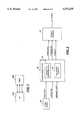
- FIG. 1is a block diagram illustrating the relationship between an image input terminal and a host terminal
- FIG. 2is a block diagram illustrating the circuit for buffering the video data from the image input terminal
- FIG. 3is a block diagram illustrating a circuit for controlling the buffering operations of the present invention
- FIG. 4is a block diagram showing the buffering operations of one embodiment of the present invention.
- FIG. 5is a block diagram illustrating a data transfer buffer circuit of a preferred embodiment of the present invention.
- FIG. 6is a block diagram illustrating a circuit for generating sensor linesync signals in the present invention.
- FIG. 7is a block diagram illustrating a circuit for generating a linesync 1 of N signal in the present invention.
- FIG. 8is a timing diagram illustrating the generation the linesync 1 of N signal in the present invention.
- FIG. 9is a block diagram illustrating one embodiment of an address control circuit for the present invention.
- FIG. 10is a block diagram illustrating a preferred embodiment of an address control circuit for the present invention.
- FIG. 1illustrates a relationship between an image input terminal 100 and a host terminal 200.
- the image input terminal (ITT) 100converts an image reflected from a document into electrical signals. These electrical signals (video data) are then transferred to the host terminal 200 serially or in parallel.
- the host terminal 200can be either a print engine, a computer processor, file server, an electronic storage device, or any electronic device capable of receiving or processing image data.
- the ITT 100 and host terminal 200communicate back and forth indicating when the host is ready for transfer as well as providing the necessary synchronization signals to bring about the transfer.
- the effective data transfer rate of the ITT terminal 100must be equal to the transfer rate of the host terminal 200.
- a synchronous transfer of data from the ITT 100 to the host terminal 200implies that scanner of the ITT 100 scans the image at a constant rate, using a constant integration time, without having to wait or stop the scanning process to allow the host terminal an opportunity to receive all the image data of a previous scanline prior to the scanner producing the next new scanline of valid image data.
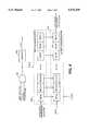
- FIG. 2illustrates a circuit used in buffering the video data received from an image sensor 80 before the video data is transferred to an output interface 50.
- video data generated by the image sensor 80is input to a line buffer 40.
- Line buffer 40includes a line buffer memory 60 and a line buffer control circuit 70.
- the line buffer memory 60in one embodiment of the present invention, is two separate scanline buffers which act in tandem to ensure proper transfer of the video data from the image sensor to the output interface 50.
- the separate scanline buffers of the preferred embodiment of the present inventionare illustrated in FIG. 5.
- one of the scanline buffersreceives video data from the image sensor 80 and temporarily stores this video data within its memory array, while the other scanline buffer outputs video data from a previous scanline to the output interface 50.
- the operations of the scanline buffersare controlled by the line buffer control circuit 70, in accordance with received image input terminal pixel clock signal and linesync 1 of N signal.
- the input terminal pixel clock signalenables the line buffer control circuit 70 to write individual pixels of video data into the scanline buffer 60.
- the linesync 1 of N signalinforms the line buffer control circuit 70 when the next scanline of video data will be input for buffering.
- FIG. 3illustrates a circuit for determining which scanlines of video data from the image sensor 80 are to be transferred to the host terminal and thus which scanlines of video data will be temporarily stored by an output scanline buffer.
- a linesync signal from the image sensor 80 of FIG. 2is input into an N-bit counter 10 and a state decoder 20.
- the N-bit counter 10outputs binary signals representing a relative scanline number within a set of scanlines.
- the N-bit counterwill output a logically active signal on the linesync/2 data line.
- the N-bit counter 10will output a logically active signal on the linesync/2 data line and the linesync/4 data line.
- the state decoder 20receives the input signals from the N-bit counter 10 and input signals from a microprocessor 30.
- the state decoder 20indicates that the scanline of valid image data being presented to a scanline buffer should be temporarily stored in this buffer.
- the number of scanlines Nis predetermined according to the difference between the normal or typical internal data transfer rate of the IIT and the data transfer rate of the host terminal.
- the resolution at which the image is to be scanned, the size of the image and the number of bits per pixelare also factors in determining N.
- the microprocessorproduces signals which causes the state decoder to produce an active level logical state image sensor linesync signal for every second state of the N-bit counter. If every fourth line of video is desired, the microprocessor produces signals which causes the decoder to select an image sensor linesync signal corresponding to every fourth state of the N-bit counter. Moreover, if a 400 line per inch image is desired at half of the normal scanline rate of the image input terminal, the optical system or the document is moved at a velocity which would generate a 800 line per inch image of which every other scanline of valid image data is discarded.
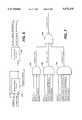
- FIG. 5illustrates a scanline buffer data transfer circuit for a preferred embodiment of the present invention.
- Pixel data from the image input terminal (IIT)is input into a latch circuit 201 which latches the data in response to an IIT pixel clock signal.
- the pixel data from latch 201is output to a bidirectional buffer 202 and a bidirectional buffer 205.
- Bidirectional buffer 202controls the flow of data between the IIT and Buffer(A) 184 as well as the flow of data from Buffer(A) 184 to the host terminal 200 through the output interface 50.
- An A/B select signalcontrols whether Buffer(A) 184 is receiving data from the IIT or is outputting data. If Buffer(A) 184 is outputting data, the data from Buffer(A) 184 is passed through bidirectional buffer 202 and input into a multiplexer 203.
- Bidirectional buffer 205operates in the same manner as bidirectional buffer 202 except that the flow of data is controlled by an inverted A/B select signal.
- bidirectional buffer 205is allowing the data stored in Buffer(B) 194 to be transferred to the host terminal 200 through the output interface 50.
- the data from Buffer(B) 194passes through bidirectional buffer 205 and is input to the multiplexer 203 when the pixel data residing in Buffer(B) 194 is to be transferred to the host terminal 200.
- Multiplexer 203selects either the data from Buffer(A) 184 or the data from Buffer(B) 194 (through the bidirectional buffers 202 and 205) in accordance with the A/B select signal.
- the data selected by multiplexer 203is latched in latch circuit 204 to enable the proper transfer of the pixel data to the host terminal 200.
- the data from latch 204is transferred to the host terminal 200 in accordance with the transfer rate required by the particular host terminal.
- FIG. 6illustrates a circuit utilized to generate the sensor linesync signal.
- a linesync signal from the IITis input into a 32 pixel clock delay circuit 110 along with the IIT pixel clock signal.
- the 32 pixel clock delay circuit 110ignores the first 32 pixels from the CCD before it produces a sensor linesync signal which indicates valid data from the CCD.
- the linesync signal that is input to the clock delay circuit 110is also used to clock a counter 120 which produces, in the preferred embodiment, two binary outputs that can be used to determine which one line of a set of four lines is to be processed.
- the outputs of counter 120are input to the circuit of FIG. 7 where they are used to select or discard sensor linesync signals.
- FIG. 7illustrates a circuit which produces the linesync 1 of N signal. More specifically, AND gates 130, 140, and 150 produce the signals linesync 1 of 1, linesync 1 of 2, and linesync 1 of 4, respectively. These signals are fed into a NOR gate 160, which produces the linesync 1 of N signal to be utilized by a buffer control unit. For example the linesync 1 of 4 signal is the result of discarding 3 of every 4 sensor linesync signals. It is noted that FIG. 7 only illustrates the generation of three separate linesync signals. This circuit can be easily modified to include any number of linesync signals by increasing the number of AND gates and adding more select (control) bits and increasing the size of the counter 120.
- FIG. 8illustrates the timing diagram of the signals generated in FIG. 7 for three separate situations.
- the linesync signalcorresponds to the signal generated by the IIT and the sensor linesync signal corresponds to the signal generated by the 32 pixel clock delay circuit 110.
- the sensor linesync signalhas the same periodicity as the linesync signal, but is delayed by 32 pixel clock cycles.
- the linesync 1 of 1 signalindicates the situation where every scanline from the image input terminal is transferred to the host terminal in a synchronous manner. In other words, the linesync 1 of 1 signal corresponds directly to the sensor linesync signal.
- the linesync 1 of 2 signalcorresponds to the situation where every other scanline of valid image data from the IIT is transferred to the host terminal.
- the linesync 1 of 2 signalis generated for every two linesync 1 of I signals.
- the linesync 1 of 4 signalcorresponds to the situation where one out of every four scanlines of valid image data generated by the IIT is transmitted to the host terminal.
- a linesync 1 of 4 signalis generated for every four linesync 1 of 1 signals.
- FIG. 9illustrates a scanline buffer address control circuit without 180 degree rotation.
- a buffer control circuit 170controls the various operations of the address control circuit in response to a host terminal clock signal, a IIT pixel clock signal, and a linesync 1 of N signal.
- the buffer control circuit 170in response to the input signals, produces a write clock signal, a read clock signal, an A/B select signal, and an A/B select inverted signal.
- the scanline buffer address control circuitincludes two counters 180 and 190.
- Counter 180is utilized to generate the write address for either Buffer(A) 184 or Buffer(B) 194.
- Counter 180is loaded with a predetermined write start address in response to the load function being activated by the linesync 1 of N signal.
- a write clock signalis also fed into counter 180 in order to change the write address.
- the write clock signalis derived from the the IIT pixel clock input to the buffer control circuit 170.
- the write address output from counter 180is fed into multiplexer 182 and multiplexer 192.
- Multiplexer 182 and 192determine whether the write address is fed to either Buffer(A) 184 or Buffer(B) 194 in response to the A/B select signal and A/B select inverted signal, respectively.
- Counter 190produces the read address to be utilized by Buffer(A) 184 and Buffer(B) 194.
- a predetermined read start addressis loaded into counter 190 in accordance with the linesync 1 of N signal activating the load function.
- a read clock signalis also fed into counter 190 in order to change the read address.
- the read clock signalis derived from the the host clock input to the buffer control circuit 170.
- the read address output from the counter 190is fed into multiplexer 182 and multiplexer 192.
- the selection of the read address for either Buffer(A) 184 or Buffer(B) 194is controlled by the A/B select signal and A/B select inverted signal, respectively.
- Buffer(A)can be storing image data from the IIT, while Buffer(B) can be transferring image data to the host terminal.
- FIG. 10illustrates a preferred embodiment of the output buffer which allows for 180° rotation in the IIT.
- a buffer control circuit 270receives a host clock signal, an IIT pixel clock signal, and a linesync 1 of N signal. From these input signals, the buffer control circuit 270 produces a write clock signal, a read clock signal, and an A/B select signal.
- FIG. 10operates in much the same manner as FIG. 9, except that FIG. 10 has two separate counters to produce the write addresses. More specifically, FIG. 10 illustrates the utilization of a writedown counter 280 and a write-up counter 295. The read counter 290 in FIG. 10 operates in the same manner as counter 190 of FIG. 9.
- FIG. 10includes two multiplexers 283 and 293. Each multiplexer receives a read address from read counter 290 and a write-up address and a write-down address from counters 295 and 280, respectively.
- An A/B select signalis also fed to the two multiplexers 283 and 293 to enable the multiplexers to choose between the read address or the write addresses.
- the A/B select signaloperates in essentially the same manner as the A/B select signal and A/B select inverted signal of FIG. 9.
- a bidirectional scan select control signalis fed to each multiplexer 283 and 293.
- the bidirectional scan select control signalenables the selection of either the write-down address when rotation is not desired or the write-up address when 180° rotation is desired.
- the image data from the IITis written into the buffer in the opposite direction from which it is read out.
- the proper addresses as selected by the multiplexers 283 and 293are fed to Buffer(A) 184 and Buffer(B) 194 so that the proper operations can be carried out as described above.
- the bidirectional scan select control signalcan be generated by either a control unit or user interface when establishing the status of the rotation state.
- FIG. 4illustrates another embodiment of the scanline buffer circuit 40 of FIG. 2.
- video data from the image sensor 80is fed into an input scanline buffer 105 containing a plurality of memory locations. More specifically, each memory address 105(1), 105(2), 105(3) . . . to 105(x-2), 105(x-1), 105(x), stores data for an individual pixel within a scanline. Data corresponding to the first pixel of a scanline is input into the memory address 105(x) and then the pixel data is shifted to the next memory location (105(x-1))in the array in response to a pixel clock signal.
- the input scanline buffer 105operates like a shift register having the capacity to hold one scanline of image data.
- the contents of input scanline buffer 105are loaded into output scanline buffer 107 with the contents of 105(x) being transferred to 107(x), the contents of 105(x-1) being transferred to 107(x-1), and the contents of 105(x-2) being transferred to 107(x-2), etc.
- the video dataAfter being loaded into the output scanline buffer 107, the video data is again shifted right in response to a second clock signal corresponding to the clock rate of the host terminal such that the video data output from the register 107(1) is serial input to the output interface 50.
- Table 1shows the situation when the internal transfer rate of the image input terminal is equal to the data transfer rate of the host terminal, a normal synchronous operation.
- image datais formed by the CCD sensors and stored in the buffer.
- the stored image data in the bufferis transferred to the host terminal.
- the array of CCD sensorsoutputs a single scanline of valid image data, d1.
- this single scanline of valid image data, d1is stored in a first buffer.
- the first bufferbegins transferring the data, d1, to the host terminal to be carried out during integration period 2, while the array of CCD sensors outputs another single scanline of valid image data, d2, wherein this single scanline of valid image data, d2, is stored in a second buffer.
- the contents of output scanline buffer 107are fully transferred to the host terminal.
- the second bufferbegins transferring data, d2, to the host terminal while the first buffer begins receiving data, d3.
- the processbegins again.
- the host terminalonly requires a single integration period to receive all the valid image data for a single scanline.
- the internal transfer rate of the image input terminalis equal to the data transfer rate of the host terminal, and a synchronous transfer can be realized.
- Table 2shows an operation where the internal transfer rate of the image input terminal is greater than the data transfer rate of the host terminal.
- image datais formed by the CCD sensors.
- not all the valid image datais stored in the buffer.
- the host terminalrequires two integration periods to properly transfer a single scanline of valid image data from the image input terminal.
- the array of CCD sensorsoutputs a single scanline of valid image data, d1.
- this single scanline of valid image data, d1is stored in a first buffer.
- the first bufferbegins transferring the data, d1, to the host terminal to be carried out during integration period 2, while the array of CCD sensors outputs another single scanline of valid image data, d2. It is noted that during integration period 2, a portion of the contents of the first buffer is transferred to the host terminal.
- the single scanline of valid image data, d2, produced during integration period 2is not stored in a buffer, but is actually skipped or discarded.
- the array of CCD sensorsoutputs another single scanline of valid image data, d3, wherein this single scanline of valid image data, d3, is stored in a second buffer during integration period 3. Moreover, the final portion of the contents of the first buffer is transferred to the host terminal. At the end of integration period 3, the second buffer begins transferring its contents, d3, to the host terminal, and the process begins again.
- the host terminalrequires two integration periods to receive all the valid image data for a single scanline.
- the internal transfer rate of the image input terminalis as much as twice the data transfer rate of the host terminal.
- skipping every other scanline of valid image data and maintaining the integration period at a constant ratea synchronous transfer can be realized.
- Table 3shows another operation where the internal transfer rate of the image input terminal is greater than the data transfer rate of the host terminal.
- the host terminalrequires four integration periods to properly transfer a single scanline of valid image data from the image input terminal.
- Table 3The situation shown in Table 3 is similar to that shown by Table 2, thus only the differences will be discussed for the sake of brevity.
- a buffertransfers approximately one fourth of its contents each integration period; therefore, the data transfer buffer circuit only stores one out of four scanlines of valid image data.
- the host terminalrequires four integration periods to receive all the valid image data for a single scanline.
- the internal transfer rate of the image input terminalis as much as four times the data transfer rate of the host terminal.
- skipping three out of four scanlines of valid image data and maintaining the integration period at a constant ratea synchronous transfer can be realized.
- the present inventionreduces the data transfer rate of the image input terminal while leaving integration time of the image sensor unchanged. This is accomplished by moving the optical system or document at a slower speed and skipping a selected number of scanlines of valid image data in a periodic manner. Thus, the image is sampled at a higher (slow scan) resolution and the data is only output periodically to allow the output interface to keep up with the data transfer rate of the image input terminal.
- the slow scan speed and periodic line sampling ratesare selected by the image input terminals microprocessor based on the volume of data which is to be produced. The volume is known based on the document size, resolution, and mode, i.e., gray or binary.
- the present inventionutilizes a binary counter and state decoder to count scanlines from the image sensing circuitry.
- the bufferis used to absorb the image input terminal video or image data, and a line signal from the image sensor 80 is used to clock a counter.
- the outputs of the counterare used in conjunction with a microprocessor which outputs signals used to derive the linesync 1 of N signal.
- the linesync 1 of N signalis generated by selecting one of every N image sensor linesync cycles where (N-1) is a number of scanlines of the valid video data to be discarded.
- a bufferwhen the linesync 1 of N signal is inactive, will not store or clock-in any data from the image sensor 80.
- the scan speed of the optics or documentis changed by the ratio of the selected lines of video data to the actual lines of video produced by the sensor.
- the function of the scanline bufferis to accept image data at the system internal data transfer rate and output image data to the image input terminal interface at the clock rate of the host terminal interface.
- the scanline buffer control circuitryis used to generate two sets of timing signals for the buffer.
- the input side of the bufferis filled with a scanline of image data in synchronism with the internal pixel transfer rate of the image input terminal.
- the output side of the bufferprovides data to the interface synchronously with a slower clock which is compatible with the host terminal.
- Image datais read from a buffer and during the entire period which the linesync 1 of N signal is both logically active and inactive.
- a scanline bufferis filled only while the linesync 1 of N signal is logically active. Therefore, the amount of time available to move a scanline of image data over to the interface is increased without sacrificing synchronization.
- the present inventionaddresses the situation of differing transfer rates by utilizing a synchronous approach.
- the present inventionsynchronously transfers image data which is scanned at a rate exceeding the transfer rate of a host terminal without experiencing the problems associated with the utilization of an asynchronous operation; the interruption of the integration period or process; and the interpolation of image data to ensure a composite line of image data.
- the image input terminalscans the entire document at a constant, but slower, rate, while maintaining and not interrupting the integration period.
- This scanning processincreases the number of scanlines of available valid image data and enables an apparent or virtual internal transfer (scan) rate equal to the data transfer rate of the host terminal, thereby providing synchronized transfer of data between devices wherein the internal transfer rate of the image input terminal exceeds the data transfer rate of the host terminal.
- the present inventionhas been described with respect to the number of discarded scanlines being equal to N-1.
- the number of scanlines to be discarded from the predetermined setcan be determined by the image input terminal based on the specifications of the data to be transferred and the transfer rate of the host terminal. If the difference is a fraction of period that is required for the image input terminal to present a scanline of data to the buffer, the discard number is rounded up to insure proper transfer to the host terminal. In other words, the transfer rate of the host terminal dominates the determination of the discard ratio.
Landscapes
- Engineering & Computer Science (AREA)
- Multimedia (AREA)
- Signal Processing (AREA)
- Image Input (AREA)
- Facsimiles In General (AREA)
- Facsimile Transmission Control (AREA)
Abstract
Description
TABLE 1 __________________________________________________________________________ INTEGR INTEGR INTEGR INTEGR INTEGR INTEGR INTEGR INTEGR INTEGR ATION ATION ATION ATION ATION ATION ATION ATION ATION PERIOD PERIOD PERIOD PERIOD PERIOD PERIOD PERIODPERIOD PERIOD DEVICE 1 2 3 4 5 6 7 8 9 __________________________________________________________________________CCD output output output output output output output output output d1 d2 d3 d4 d5 d6 d7 d8 d9 BUFFER store store store store store store store store store d1 d2 d3 d4 d5 d6 d7 d8 d9 I/O X output output output output output output output output d1 d2 d3 d4 d5 d6 d7 d8 __________________________________________________________________________
TABLE 2 __________________________________________________________________________ INTEGR INTEGR INTEGR INTEGR INTEGR INTEGR INTEGR INTEGR INTEGR ATION ATION ATION ATION ATION ATION ATION ATION ATION PERIOD PERIOD PERIOD PERIOD PERIOD PERIOD PERIODPERIOD PERIOD DEVICE 1 2 3 4 5 6 7 8 9 __________________________________________________________________________CCD output output output output output output output output output d1 d2 d3 d4 d5 d6 d7 d8 d9 BUFFER Store skip d2 store skip d4 store skip d6 store skip d8 store d1 d3 d5 d7 d9 I/O X output output output output output output output output d1 d1 d3 d3 d5 d5 d7 d7 __________________________________________________________________________
TABLE 3 __________________________________________________________________________ INTEGR INTEGR INTEGR INTEGR INTEGR INTEGR INTEGR INTEGR INTEGR ATION ATION ATION ATION ATION ATION ATION ATION ATION PERIOD PERIOD PERIOD PERIOD PERIOD PERIOD PERIODPERIOD PERIOD DEVICE 1 2 3 4 5 6 7 8 9 __________________________________________________________________________CCD output output output output output output output output output d1 d2 d3 d4 d5 d6 d7 d8 d9 BUFFER store skip d2 skip d3 skip d4 store skip d6 skip d7 skip d8 store d1 d5 d9 I/O X output output output output output output output output d1 d1 d1 d1 d5 d5 d5 d5 __________________________________________________________________________
Claims (22)
Priority Applications (6)
| Application Number | Priority Date | Filing Date | Title |
|---|---|---|---|
| US08/222,200US5572335A (en) | 1994-04-01 | 1994-04-01 | Method and system for transferring image data between two devices having different bandwidths |
| MX9501506AMX9501506A (en) | 1994-04-01 | 1995-03-24 | Device and method for controlling the scan speed of an image input terminal to match the clock rate of a host interface. |
| JP7073948AJPH07311843A (en) | 1994-04-01 | 1995-03-30 | Apparatus and method for control so as to match scanning speed of image input terminal with clock rate of host interface |
| BR9501405ABR9501405A (en) | 1994-04-01 | 1995-03-31 | System and process for transferring video data from an image input terminal to a main terminal |
| EP95302179AEP0675634B1 (en) | 1994-04-01 | 1995-03-31 | System and method for transferring digital data between an image input terminal and a host terminal |
| DE69519759TDE69519759T2 (en) | 1994-04-01 | 1995-03-31 | System and method for transferring digital data between an image input terminal and a host terminal |
Applications Claiming Priority (1)
| Application Number | Priority Date | Filing Date | Title |
|---|---|---|---|
| US08/222,200US5572335A (en) | 1994-04-01 | 1994-04-01 | Method and system for transferring image data between two devices having different bandwidths |
Publications (1)
| Publication Number | Publication Date |
|---|---|
| US5572335Atrue US5572335A (en) | 1996-11-05 |
Family
ID=22831290
Family Applications (1)
| Application Number | Title | Priority Date | Filing Date |
|---|---|---|---|
| US08/222,200Expired - LifetimeUS5572335A (en) | 1994-04-01 | 1994-04-01 | Method and system for transferring image data between two devices having different bandwidths |
Country Status (6)
| Country | Link |
|---|---|
| US (1) | US5572335A (en) |
| EP (1) | EP0675634B1 (en) |
| JP (1) | JPH07311843A (en) |
| BR (1) | BR9501405A (en) |
| DE (1) | DE69519759T2 (en) |
| MX (1) | MX9501506A (en) |
Cited By (35)
| Publication number | Priority date | Publication date | Assignee | Title |
|---|---|---|---|---|
| US5668637A (en)* | 1995-03-22 | 1997-09-16 | Canon Kabushiki Kaisha | Image processing apparatus having a copy function |
| US6256106B1 (en)* | 1997-04-30 | 2001-07-03 | Ricoh Company, Ltd. | Two-way image processing system and image forming apparatus in such a system |
| US6285465B1 (en)* | 1993-07-05 | 2001-09-04 | Canon Kabushiki Kaisha | Facsimile apparatus which corrects read image data based on a difference between a predetermined storage time and a recording time of the read image data |
| US6335807B1 (en)* | 1998-11-30 | 2002-01-01 | Agfa Corporation | Scanner carriage stop/start artifact suppression system and method |
| US6388777B1 (en)* | 1997-12-15 | 2002-05-14 | Ricoh Corporation, Ltd. | Digital image reading apparatus |
| US20040042051A1 (en)* | 2002-08-28 | 2004-03-04 | Cheng-Kuei Chen | Method for determining restored position |
| WO2005018061A3 (en)* | 2003-08-11 | 2005-11-03 | Raydiance Inc | Pumping of optically-pumped amplifiers |
| US20050259980A1 (en)* | 2000-06-20 | 2005-11-24 | Yoshiyuki Sasaki | Information reproducing method and apparatus |
| US7115514B2 (en) | 2003-10-02 | 2006-10-03 | Raydiance, Inc. | Semiconductor manufacturing using optical ablation |
| US7139116B1 (en) | 2005-11-30 | 2006-11-21 | Raydiance,Inc. | Post amplification optical isolator |
| US7143769B2 (en) | 2003-08-11 | 2006-12-05 | Richard Stoltz | Controlling pulse energy of an optical amplifier by controlling pump diode current |
| US7245419B2 (en) | 2005-09-22 | 2007-07-17 | Raydiance, Inc. | Wavelength-stabilized pump diodes for pumping gain media in an ultrashort pulsed laser system |
| US7308171B2 (en) | 2005-11-16 | 2007-12-11 | Raydiance, Inc. | Method and apparatus for optical isolation in high power fiber-optic systems |
| US20080065423A1 (en)* | 2006-09-07 | 2008-03-13 | Yoshihiro Oda | Image use history management system, modality, and server |
| US7349452B2 (en) | 2004-12-13 | 2008-03-25 | Raydiance, Inc. | Bragg fibers in systems for the generation of high peak power light |
| US7361171B2 (en) | 2003-05-20 | 2008-04-22 | Raydiance, Inc. | Man-portable optical ablation system |
| US7367969B2 (en) | 2003-08-11 | 2008-05-06 | Raydiance, Inc. | Ablative material removal with a preset removal rate or volume or depth |
| US7413847B2 (en) | 2004-02-09 | 2008-08-19 | Raydiance, Inc. | Semiconductor-type processing for solid-state lasers |
| US20100238519A1 (en)* | 2001-07-31 | 2010-09-23 | Kuo-Jeng Wang | Scanning speed control device and method |
| US8125704B2 (en) | 2008-08-18 | 2012-02-28 | Raydiance, Inc. | Systems and methods for controlling a pulsed laser by combining laser signals |
| US8135050B1 (en) | 2005-07-19 | 2012-03-13 | Raydiance, Inc. | Automated polarization correction |
| US8139910B2 (en) | 2006-01-23 | 2012-03-20 | Raydiance, Inc. | Systems and methods for control of ultra short pulse amplification |
| US20120075680A1 (en)* | 2001-07-31 | 2012-03-29 | Transpacific Systems, Llc | Scanning speed control device and method |
| US8150271B1 (en) | 2006-03-28 | 2012-04-03 | Raydiance, Inc. | Active tuning of temporal dispersion in an ultrashort pulse laser system |
| US8173929B1 (en) | 2003-08-11 | 2012-05-08 | Raydiance, Inc. | Methods and systems for trimming circuits |
| US8189971B1 (en) | 2006-01-23 | 2012-05-29 | Raydiance, Inc. | Dispersion compensation in a chirped pulse amplification system |
| US8232687B2 (en) | 2006-04-26 | 2012-07-31 | Raydiance, Inc. | Intelligent laser interlock system |
| US8498538B2 (en) | 2008-11-14 | 2013-07-30 | Raydiance, Inc. | Compact monolithic dispersion compensator |
| US8619357B2 (en) | 2007-11-30 | 2013-12-31 | Raydiance, Inc. | Static phase mask for high-order spectral phase control in a hybrid chirped pulse amplifier system |
| US20140168693A1 (en)* | 2012-12-17 | 2014-06-19 | Canon Kabushiki Kaisha | Printing apparatus and control method thereof, image processing apparatus, image processing method, and non-transitory computer-readable medium |
| US9022037B2 (en) | 2003-08-11 | 2015-05-05 | Raydiance, Inc. | Laser ablation method and apparatus having a feedback loop and control unit |
| US9114482B2 (en) | 2010-09-16 | 2015-08-25 | Raydiance, Inc. | Laser based processing of layered materials |
| US9130344B2 (en) | 2006-01-23 | 2015-09-08 | Raydiance, Inc. | Automated laser tuning |
| US20150310820A1 (en)* | 2014-04-24 | 2015-10-29 | Focaltech Systems, Ltd. | Driving circuit, driving method, display apparatus and electronic apparatus |
| US10239160B2 (en) | 2011-09-21 | 2019-03-26 | Coherent, Inc. | Systems and processes that singulate materials |
Families Citing this family (3)
| Publication number | Priority date | Publication date | Assignee | Title |
|---|---|---|---|---|
| IES72079B2 (en)* | 1996-11-06 | 1997-03-12 | Tangate Limited | Apparatus for capturing a frame of video data for sending to a printer |
| JPH10257289A (en)* | 1997-03-11 | 1998-09-25 | Murata Mach Ltd | Facsimile equipment |
| JPH1155485A (en)* | 1997-07-29 | 1999-02-26 | Canon Inc | Information processing apparatus, information processing method, and storage medium storing computer readable program |
Citations (17)
| Publication number | Priority date | Publication date | Assignee | Title |
|---|---|---|---|---|
| US3428744A (en)* | 1965-07-14 | 1969-02-18 | Xerox Corp | Facsimile line skipping system |
| US3436474A (en)* | 1965-10-01 | 1969-04-01 | Xerox Corp | Facsimile optional double skipping |
| US3502803A (en)* | 1967-05-12 | 1970-03-24 | Xerox Corp | Facsimile line skipping apparatus |
| US3524926A (en)* | 1966-06-15 | 1970-08-18 | Xerox Corp | System for delta encoding at selected intervals |
| US3902009A (en)* | 1974-06-17 | 1975-08-26 | Xerox Corp | Multi aperture scanning and printing for facsimile line skipping |
| US4367493A (en)* | 1981-04-02 | 1983-01-04 | Xerox Corporation | Raster scanner apparatus and method |
| US4541061A (en)* | 1982-10-13 | 1985-09-10 | Minnesota Mining And Manufacturing Company | Data clocking circuitry for a scanning apparatus |
| US4587415A (en)* | 1982-07-23 | 1986-05-06 | Canon Kabushiki Kaisha | Photo-detecting device with storage time control |
| US4628368A (en)* | 1983-07-12 | 1986-12-09 | Fuji Xerox Co., Ltd. | Method for controlling sub-scanning of document reading apparatus |
| US4748514A (en)* | 1986-12-22 | 1988-05-31 | Xerox Corporation | Variable rate scanning control |
| US4878119A (en)* | 1988-02-29 | 1989-10-31 | Xerox Corporation | System for synchronizing integration pulses with integration signal in an asynchronous raster input scanner |
| US4910607A (en)* | 1986-09-30 | 1990-03-20 | Sharp Kabushiki Kaisha | Image processing device of multifunctional type |
| US5043827A (en)* | 1989-08-03 | 1991-08-27 | Xerox Corporation | Combined asynchronous-synchronous document scanner |
| US5113260A (en)* | 1990-12-24 | 1992-05-12 | Xerox Corporation | Sensor array for both synchronous and asynchronous operation |
| EP0507439A2 (en)* | 1991-03-07 | 1992-10-07 | Hewlett-Packard Company | Buffering control for accommodating variable data exchange rates |
| US5278974A (en)* | 1989-12-04 | 1994-01-11 | Digital Equipment Corporation | Method and apparatus for the dynamic adjustment of data transfer timing to equalize the bandwidths of two buses in a computer system having different bandwidths |
| US5369504A (en)* | 1992-04-09 | 1994-11-29 | Xerox Corporation | Method and apparatus for reducing image distortion in an asynchronous input scanner |
Family Cites Families (2)
| Publication number | Priority date | Publication date | Assignee | Title |
|---|---|---|---|---|
| JPH01264062A (en)* | 1988-04-14 | 1989-10-20 | Tokyo Electric Co Ltd | Original moving type image reading device |
| JP3289933B2 (en)* | 1991-12-11 | 2002-06-10 | 株式会社リコー | Image transmission device |
- 1994
- 1994-04-01USUS08/222,200patent/US5572335A/ennot_activeExpired - Lifetime
- 1995
- 1995-03-24MXMX9501506Apatent/MX9501506A/enunknown
- 1995-03-30JPJP7073948Apatent/JPH07311843A/enactivePending
- 1995-03-31EPEP95302179Apatent/EP0675634B1/ennot_activeExpired - Lifetime
- 1995-03-31BRBR9501405Apatent/BR9501405A/ennot_activeIP Right Cessation
- 1995-03-31DEDE69519759Tpatent/DE69519759T2/ennot_activeExpired - Lifetime
Patent Citations (19)
| Publication number | Priority date | Publication date | Assignee | Title |
|---|---|---|---|---|
| US3428744A (en)* | 1965-07-14 | 1969-02-18 | Xerox Corp | Facsimile line skipping system |
| US3436474A (en)* | 1965-10-01 | 1969-04-01 | Xerox Corp | Facsimile optional double skipping |
| US3524926A (en)* | 1966-06-15 | 1970-08-18 | Xerox Corp | System for delta encoding at selected intervals |
| US3502803A (en)* | 1967-05-12 | 1970-03-24 | Xerox Corp | Facsimile line skipping apparatus |
| US3902009A (en)* | 1974-06-17 | 1975-08-26 | Xerox Corp | Multi aperture scanning and printing for facsimile line skipping |
| US4367493A (en)* | 1981-04-02 | 1983-01-04 | Xerox Corporation | Raster scanner apparatus and method |
| US4587415A (en)* | 1982-07-23 | 1986-05-06 | Canon Kabushiki Kaisha | Photo-detecting device with storage time control |
| US4541061A (en)* | 1982-10-13 | 1985-09-10 | Minnesota Mining And Manufacturing Company | Data clocking circuitry for a scanning apparatus |
| US4628368A (en)* | 1983-07-12 | 1986-12-09 | Fuji Xerox Co., Ltd. | Method for controlling sub-scanning of document reading apparatus |
| US4910607A (en)* | 1986-09-30 | 1990-03-20 | Sharp Kabushiki Kaisha | Image processing device of multifunctional type |
| US5021892A (en)* | 1986-09-30 | 1991-06-04 | Sharp Kabushiki Kaisha | Image processing device of multifunctional type |
| US4748514A (en)* | 1986-12-22 | 1988-05-31 | Xerox Corporation | Variable rate scanning control |
| US4878119A (en)* | 1988-02-29 | 1989-10-31 | Xerox Corporation | System for synchronizing integration pulses with integration signal in an asynchronous raster input scanner |
| US5043827A (en)* | 1989-08-03 | 1991-08-27 | Xerox Corporation | Combined asynchronous-synchronous document scanner |
| US5239387A (en)* | 1989-11-30 | 1993-08-24 | Hewlett-Packard Company | Buffering control for accommodating variable data exchange rates |
| US5278974A (en)* | 1989-12-04 | 1994-01-11 | Digital Equipment Corporation | Method and apparatus for the dynamic adjustment of data transfer timing to equalize the bandwidths of two buses in a computer system having different bandwidths |
| US5113260A (en)* | 1990-12-24 | 1992-05-12 | Xerox Corporation | Sensor array for both synchronous and asynchronous operation |
| EP0507439A2 (en)* | 1991-03-07 | 1992-10-07 | Hewlett-Packard Company | Buffering control for accommodating variable data exchange rates |
| US5369504A (en)* | 1992-04-09 | 1994-11-29 | Xerox Corporation | Method and apparatus for reducing image distortion in an asynchronous input scanner |
Non-Patent Citations (2)
| Title |
|---|
| Patent Abstract of Japan, Kamishiro Toshiaki, Title: Image Transmission Equipment. ab. Date: Oct. 20, 1993, p. 1.* |
| Patent Abstract of Japan, Uchida Seigo; others: Title: Original Moving Type Picture Reader, ab. Date: Jan. 17, 1990, p. 1.* |
Cited By (46)
| Publication number | Priority date | Publication date | Assignee | Title |
|---|---|---|---|---|
| US6285465B1 (en)* | 1993-07-05 | 2001-09-04 | Canon Kabushiki Kaisha | Facsimile apparatus which corrects read image data based on a difference between a predetermined storage time and a recording time of the read image data |
| US5668637A (en)* | 1995-03-22 | 1997-09-16 | Canon Kabushiki Kaisha | Image processing apparatus having a copy function |
| US6256106B1 (en)* | 1997-04-30 | 2001-07-03 | Ricoh Company, Ltd. | Two-way image processing system and image forming apparatus in such a system |
| US6388777B1 (en)* | 1997-12-15 | 2002-05-14 | Ricoh Corporation, Ltd. | Digital image reading apparatus |
| US6335807B1 (en)* | 1998-11-30 | 2002-01-01 | Agfa Corporation | Scanner carriage stop/start artifact suppression system and method |
| US20060280432A1 (en)* | 2000-06-20 | 2006-12-14 | Yoshiyuki Sasaki | Information reproducing method and apparatus |
| US20050259980A1 (en)* | 2000-06-20 | 2005-11-24 | Yoshiyuki Sasaki | Information reproducing method and apparatus |
| US7808864B2 (en) | 2000-06-20 | 2010-10-05 | Ricoh Company, Ltd. | Information reproducing method and apparatus |
| US7593297B2 (en) | 2000-06-20 | 2009-09-22 | Ricoh Company, Ltd. | Information reproducing method and apparatus |
| US8355183B2 (en)* | 2001-07-31 | 2013-01-15 | Transpacific Systems, Llc | Scanning speed control device and method |
| US8218183B2 (en) | 2001-07-31 | 2012-07-10 | Transpacific Systems, Llc | Scanning speed control device and method |
| US20120075680A1 (en)* | 2001-07-31 | 2012-03-29 | Transpacific Systems, Llc | Scanning speed control device and method |
| US20100238519A1 (en)* | 2001-07-31 | 2010-09-23 | Kuo-Jeng Wang | Scanning speed control device and method |
| US7136200B2 (en)* | 2002-08-28 | 2006-11-14 | Cheng-Kuei Chen | Method for determining restored scanning position |
| US20040042051A1 (en)* | 2002-08-28 | 2004-03-04 | Cheng-Kuei Chen | Method for determining restored position |
| US20070064284A1 (en)* | 2002-08-28 | 2007-03-22 | Transpacific Ip, Ltd. | Method for determining restored scanning position |
| US8398622B2 (en) | 2003-05-20 | 2013-03-19 | Raydiance, Inc. | Portable optical ablation system |
| US7361171B2 (en) | 2003-05-20 | 2008-04-22 | Raydiance, Inc. | Man-portable optical ablation system |
| US7143769B2 (en) | 2003-08-11 | 2006-12-05 | Richard Stoltz | Controlling pulse energy of an optical amplifier by controlling pump diode current |
| US9022037B2 (en) | 2003-08-11 | 2015-05-05 | Raydiance, Inc. | Laser ablation method and apparatus having a feedback loop and control unit |
| US7367969B2 (en) | 2003-08-11 | 2008-05-06 | Raydiance, Inc. | Ablative material removal with a preset removal rate or volume or depth |
| WO2005018061A3 (en)* | 2003-08-11 | 2005-11-03 | Raydiance Inc | Pumping of optically-pumped amplifiers |
| US8173929B1 (en) | 2003-08-11 | 2012-05-08 | Raydiance, Inc. | Methods and systems for trimming circuits |
| US7115514B2 (en) | 2003-10-02 | 2006-10-03 | Raydiance, Inc. | Semiconductor manufacturing using optical ablation |
| US7413847B2 (en) | 2004-02-09 | 2008-08-19 | Raydiance, Inc. | Semiconductor-type processing for solid-state lasers |
| US7349452B2 (en) | 2004-12-13 | 2008-03-25 | Raydiance, Inc. | Bragg fibers in systems for the generation of high peak power light |
| US8135050B1 (en) | 2005-07-19 | 2012-03-13 | Raydiance, Inc. | Automated polarization correction |
| US7245419B2 (en) | 2005-09-22 | 2007-07-17 | Raydiance, Inc. | Wavelength-stabilized pump diodes for pumping gain media in an ultrashort pulsed laser system |
| US7308171B2 (en) | 2005-11-16 | 2007-12-11 | Raydiance, Inc. | Method and apparatus for optical isolation in high power fiber-optic systems |
| US7436866B2 (en) | 2005-11-30 | 2008-10-14 | Raydiance, Inc. | Combination optical isolator and pulse compressor |
| US7139116B1 (en) | 2005-11-30 | 2006-11-21 | Raydiance,Inc. | Post amplification optical isolator |
| US8189971B1 (en) | 2006-01-23 | 2012-05-29 | Raydiance, Inc. | Dispersion compensation in a chirped pulse amplification system |
| US8139910B2 (en) | 2006-01-23 | 2012-03-20 | Raydiance, Inc. | Systems and methods for control of ultra short pulse amplification |
| US9130344B2 (en) | 2006-01-23 | 2015-09-08 | Raydiance, Inc. | Automated laser tuning |
| US8150271B1 (en) | 2006-03-28 | 2012-04-03 | Raydiance, Inc. | Active tuning of temporal dispersion in an ultrashort pulse laser system |
| US8232687B2 (en) | 2006-04-26 | 2012-07-31 | Raydiance, Inc. | Intelligent laser interlock system |
| US9281653B2 (en) | 2006-04-26 | 2016-03-08 | Coherent, Inc. | Intelligent laser interlock system |
| US20080065423A1 (en)* | 2006-09-07 | 2008-03-13 | Yoshihiro Oda | Image use history management system, modality, and server |
| US8619357B2 (en) | 2007-11-30 | 2013-12-31 | Raydiance, Inc. | Static phase mask for high-order spectral phase control in a hybrid chirped pulse amplifier system |
| US8125704B2 (en) | 2008-08-18 | 2012-02-28 | Raydiance, Inc. | Systems and methods for controlling a pulsed laser by combining laser signals |
| US8498538B2 (en) | 2008-11-14 | 2013-07-30 | Raydiance, Inc. | Compact monolithic dispersion compensator |
| US9114482B2 (en) | 2010-09-16 | 2015-08-25 | Raydiance, Inc. | Laser based processing of layered materials |
| US10239160B2 (en) | 2011-09-21 | 2019-03-26 | Coherent, Inc. | Systems and processes that singulate materials |
| US20140168693A1 (en)* | 2012-12-17 | 2014-06-19 | Canon Kabushiki Kaisha | Printing apparatus and control method thereof, image processing apparatus, image processing method, and non-transitory computer-readable medium |
| US20150310820A1 (en)* | 2014-04-24 | 2015-10-29 | Focaltech Systems, Ltd. | Driving circuit, driving method, display apparatus and electronic apparatus |
| US9495928B2 (en)* | 2014-04-24 | 2016-11-15 | Focaltech Systems, Ltd. | Driving circuit, driving method, display apparatus and electronic apparatus |
Also Published As
| Publication number | Publication date |
|---|---|
| EP0675634B1 (en) | 2001-01-03 |
| EP0675634A2 (en) | 1995-10-04 |
| DE69519759T2 (en) | 2001-06-13 |
| MX9501506A (en) | 1997-08-30 |
| DE69519759D1 (en) | 2001-02-08 |
| EP0675634A3 (en) | 1996-03-27 |
| BR9501405A (en) | 1995-12-19 |
| JPH07311843A (en) | 1995-11-28 |
Similar Documents
| Publication | Publication Date | Title |
|---|---|---|
| US5572335A (en) | Method and system for transferring image data between two devices having different bandwidths | |
| MXPA95001506A (en) | Device and method for controlling the exploring speed of a deimagen entry terminal for balancing the de-synchronization speed of a principle interface | |
| US5043827A (en) | Combined asynchronous-synchronous document scanner | |
| US5901274A (en) | Method for enlargement/reduction of image data in digital image processing system and circuit adopting the same | |
| US5293432A (en) | Document image scanner with variable resolution windows | |
| US5647026A (en) | Uniformity correction and threshold or halftoning conversion unit and method | |
| JPH0813082B2 (en) | Raster input scanner asynchronous operation method and scanning device | |
| GB2183961A (en) | Image reading and/or recording apparatus with enlarging and reducing function | |
| US5604608A (en) | Device and method for controlling the scan speed of an image input terminal to match the throughput constraints of an image processing module | |
| US5101282A (en) | Variable magnification image | |
| JP3585976B2 (en) | Image reading device | |
| US20070019093A1 (en) | High-speed image pickup method and controller for image pickup device | |
| US6914632B1 (en) | Apparatus for panning and scaling window in image sensor | |
| EP0966150A2 (en) | Image processing apparatus and image processing method, and storage media thereof | |
| US5349449A (en) | Image data processing circuit and method of accessing storing means for the processing circuit | |
| US4947267A (en) | Image reading apparatus | |
| EP0767577B1 (en) | Image processing apparatus with image enlargement function | |
| US5712714A (en) | Image processing apparatus | |
| US5764370A (en) | Enlargement and reduction apparatus for an image forming apparatus | |
| JP2882532B2 (en) | Image data processing device | |
| JP3631512B2 (en) | Data processing device | |
| JP3913533B2 (en) | Digital copying machine | |
| KR100242116B1 (en) | Variable magnification photo-recorder | |
| KR100438161B1 (en) | scanning apparatus | |
| JPH047965A (en) | Printer controller |
Legal Events
| Date | Code | Title | Description |
|---|---|---|---|
| AS | Assignment | Owner name:XEROX CORPORATION, CONNECTICUT Free format text:ASSIGNMENT OF ASSIGNORS INTEREST;ASSIGNOR:STEVENS, JAMES W.;REEL/FRAME:006947/0636 Effective date:19940401 | |
| STCF | Information on status: patent grant | Free format text:PATENTED CASE | |
| FPAY | Fee payment | Year of fee payment:4 | |
| AS | Assignment | Owner name:BANK ONE, NA, AS ADMINISTRATIVE AGENT, ILLINOIS Free format text:SECURITY INTEREST;ASSIGNOR:XEROX CORPORATION;REEL/FRAME:013153/0001 Effective date:20020621 | |
| AS | Assignment | Owner name:JPMORGAN CHASE BANK, AS COLLATERAL AGENT, TEXAS Free format text:SECURITY AGREEMENT;ASSIGNOR:XEROX CORPORATION;REEL/FRAME:015134/0476 Effective date:20030625 Owner name:JPMORGAN CHASE BANK, AS COLLATERAL AGENT,TEXAS Free format text:SECURITY AGREEMENT;ASSIGNOR:XEROX CORPORATION;REEL/FRAME:015134/0476 Effective date:20030625 | |
| FPAY | Fee payment | Year of fee payment:8 | |
| FPAY | Fee payment | Year of fee payment:12 | |
| AS | Assignment | Owner name:XEROX CORPORATION, CONNECTICUT Free format text:RELEASE BY SECURED PARTY;ASSIGNOR:JPMORGAN CHASE BANK, N.A. AS SUCCESSOR-IN-INTEREST ADMINISTRATIVE AGENT AND COLLATERAL AGENT TO JPMORGAN CHASE BANK;REEL/FRAME:066728/0193 Effective date:20220822 |