US5572160A - Architecture for RF signal automatic test equipment - Google Patents
Architecture for RF signal automatic test equipmentDownload PDFInfo
- Publication number
- US5572160A US5572160AUS08/347,633US34763394AUS5572160AUS 5572160 AUS5572160 AUS 5572160AUS 34763394 AUS34763394 AUS 34763394AUS 5572160 AUS5572160 AUS 5572160A
- Authority
- US
- United States
- Prior art keywords
- channel
- directional
- type
- signal
- port
- Prior art date
- Legal status (The legal status is an assumption and is not a legal conclusion. Google has not performed a legal analysis and makes no representation as to the accuracy of the status listed.)
- Expired - Lifetime
Links
- 238000012360testing methodMethods0.000titleclaimsabstractdescription66
- 230000004044responseEffects0.000claimsdescription5
- 230000008878couplingEffects0.000claims1
- 238000010168coupling processMethods0.000claims1
- 238000005859coupling reactionMethods0.000claims1
- 238000005259measurementMethods0.000abstractdescription34
- 238000000034methodMethods0.000description10
- 230000006870functionEffects0.000description7
- 230000008569processEffects0.000description6
- 238000013461designMethods0.000description5
- 239000004065semiconductorSubstances0.000description5
- 239000007787solidSubstances0.000description5
- 238000010586diagramMethods0.000description4
- 238000004519manufacturing processMethods0.000description4
- 230000008901benefitEffects0.000description3
- 230000007246mechanismEffects0.000description2
- 238000003012network analysisMethods0.000description2
- 230000004913activationEffects0.000description1
- 238000004458analytical methodMethods0.000description1
- 238000004364calculation methodMethods0.000description1
- 230000001413cellular effectEffects0.000description1
- 230000006835compressionEffects0.000description1
- 238000007906compressionMethods0.000description1
- 238000007796conventional methodMethods0.000description1
- 230000007423decreaseEffects0.000description1
- 238000005516engineering processMethods0.000description1
- 230000003993interactionEffects0.000description1
- 238000012545processingMethods0.000description1
- 238000005070samplingMethods0.000description1
- 238000001228spectrumMethods0.000description1
Images


Classifications
- G—PHYSICS
- G01—MEASURING; TESTING
- G01R—MEASURING ELECTRIC VARIABLES; MEASURING MAGNETIC VARIABLES
- G01R31/00—Arrangements for testing electric properties; Arrangements for locating electric faults; Arrangements for electrical testing characterised by what is being tested not provided for elsewhere
- G01R31/28—Testing of electronic circuits, e.g. by signal tracer
- G01R31/3167—Testing of combined analog and digital circuits
- G—PHYSICS
- G01—MEASURING; TESTING
- G01R—MEASURING ELECTRIC VARIABLES; MEASURING MAGNETIC VARIABLES
- G01R27/00—Arrangements for measuring resistance, reactance, impedance, or electric characteristics derived therefrom
- G01R27/28—Measuring attenuation, gain, phase shift or derived characteristics of electric four pole networks, i.e. two-port networks; Measuring transient response
- G01R27/32—Measuring attenuation, gain, phase shift or derived characteristics of electric four pole networks, i.e. two-port networks; Measuring transient response in circuits having distributed constants, e.g. having very long conductors or involving high frequencies
Definitions
- This inventionrelates generally to automatic test equipment and more specifically to an architecture for providing high frequency test signals to a device under test.
- TesterAutomatic test equipment
- Purely digital devicesare usually tested with testers which drive and receive digital signals.
- Semiconductor devices which process analog as well as digital signalsmust be tested with testers which can produce and receive analog and digital signals. These signals are called mixed signal testers.
- FIG. 1shows the architecture of a typical prior art mixed signal tester 100.
- Tester main frame 102controls the test. It generates test signals and analyzes responses to identify errors during a test.
- Tester main frame 102is connected to the device under test (herein a "DUT") 106 through test head 104.
- DUTdevice under test
- Test head 104routes the various test signals needed to test DUT 106 into this small area. Test head 104 also contains electronic circuitry which must be positioned close to DUT 106 to provide good signal integrity.
- Tester 100is controlled by control electronics 108 inside tester main frame 102.
- Control electronics 108is a high speed computer. It includes memory (not shown) which can be programmed so that tester 100 can perform numerous tests on a variety of semiconductor devices.
- Tester 100includes subsystems that process RF signals. RF signals are loosely defined as those signals having frequencies in the range of about 10 MHz up to about 6 GHz. Tester 100 also includes a subsystem that processes lower frequency AC signals, sometimes called base band signals. Tester 100 also contains a subsystem that processes DC signals and another subsystem that processes digital signals.
- the RF subsystemis made up of a plurality of RF sources and receivers 112. Each RF source can be programmed to generate a test signal at a frequency and level specified by control electronics 108. Some or all of the RF sources receive a base band signal from the low frequency subsystem over signal path 136. This base band signal is used to modulate the RF signal provided by the source.
- Each RF receivermeasures power of a received signal over a range of frequencies.
- the operating parameters of the source and receivercan be controlled by control electronics 108. Some or all of the receivers can also down convert the RF signal to a base band signal which is passed to the low frequency subsystem.
- each of the dedicated instruments 120generally performs one function, such as vector network analysis. More recently, some dedicated instruments which perform two functions have become available. These instruments often have a standard control interface such as VXI or gpib so that they may be easily incorporated into tester 100.
- the low frequency (base band) subsystemis made up of low frequency analog sources and receivers 114. These devices are implemented using digital signal processing technology. A typical system might operate at 200 MHz, allowing waveforms of almost any shape to be produced or analyzed.
- the DC subsystemis made up of DC sources and meters 116. These devices can produce or measure DC bias conditions.
- the digital subsystemgenerates and receives digital signals. It is made up of digital drivers and receivers 116.
- test head 104contains distributed instrument electronics 122, which represent portions of the sources or receivers in the RF, low frequency, DC and digital subsystems that must be positioned near DUT 106 for greater accuracy or other reasons.
- RF switching circuitry 134Connections to the RF sources and receivers 112 and the dedicated instruments 120 are made through RF switching circuitry 134.
- Each lead (not numbered) of DUT 106which receives or produces an RF signal is connected to RF switching circuitry 134.
- the RF subsystemmust be configured differently for each test. The configuration is created by moving cables and opening and closing switches inside RF switching circuitry 134. These switches operate under control of control electronics 108. These switches are typically implemented with commercially available microwave switches. The switches are configured to allow each source or receiver used to test one lead of DUT 106 to be connected to that lead.
- interconnect circuitry 132contains switches to make the appropriate connections.
- Interconnect circuitry 132is connected to RF switching circuitry through signal path 138.
- Signal path 138allows DC bias conditions to be introduced or measured within the RF subsystem.
- control electronics 108executes a program.
- the programconfigures tester 100 to make a first measurement by specifying the settings for the instruments 112, 114, 116, 118 and 120 and also the settings for switches in RF switching circuitry 134 and interconnect circuitry 132. The measurement is made and passed back to control electronics 108. Then, tester 100 is reconfigured to take the next measurement. This process is repeated until all the required measurements are taken.
- Custom RF switching 134is undesirable for several reasons. First, the instruments used to test a particular semiconductor device will depend on the type of device used. As a result, RF switching circuit 134 must be custom made for each type of device tested. There is a significant cost associated with preparing custom hardware and software needed to control it.
- RF test instrumentsnormally include software calibration routines. Those routines, however, calibrate the instrument only for tests in which the DUT is connected directly to the instrument. Different calibration routines must be written to account for the switching circuitry between the instrument and DUT 106. Because this switching circuitry is custom built for each type of device to be tested, the calibration routines must also be custom written for the type of device to be tested.
- a third disadvantageis that RF switching circuitry 134 is constructed from numerous microwave switches. These switches are generally large, which makes it difficult to place them close to DUT 106. As a result, distributed instrument electronics 122 must be spaced away from DUT 106 further than might be desirable. In addition, the microwave switches are slow to operate, which decreases the number of devices which can be tested in a manufacturing shift. Further, microwave switches are also expensive and unreliable. They are prone to fail or have degraded performance after as little as a few hundred thousand operations.
- a further disadvantage with the architecture of FIG. 1is the cost of dedicated instruments 120. It would be highly desirable if more measurements could be made with the RF sources and receivers 112.
- a modulehaving a first input connected to an RF source and a second input allowing connection of a second RF source.
- the modulealso includes a directional element connected in the signal path from the source. Two ports of the directional element are connected to a receiver through a switch, allowing forward and backwards signals to be measured. Another port of the directional element is connected to the test point through a bias T-circuit, which allows introduction and measurement of DC bias conditions.
- multiple modulesare used in a mixed signal tester which includes a plurality of RF channels.
- Each channel or a group of a small number of channelshas associated with it an RF source and an RF receiver connected to the module.
- the architectureallows there to be a different number of sources and receivers per channel or group of channels.
- Each moduleadditionally includes switching elements which allow the source from one channel to be connected as the second RF source in another channel.
- each moduleis implemented with solid state elements.
- one or more switchesare included in the signal path which can be used to calibrate each source and receiver.
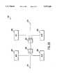
- FIG. 1is a block diagram of a mixed signal tester which could employ the invention
- FIG. 2Ais a schematic diagram of an RF module according to the; invention.
- FIG. 2Bis a schematic diagram of the calibration module used in the RF module of FIG. 2A.
- RF switching circuitry 134is replaced by one or more channel cards.
- Each channel cardcontains one or more circuits, called “channels,” designed to send and receive RF signals to one lead of DUT 106.
- Each channel cardhas an architecture which allows sources and receivers to be connected to the DUT in a large number of ways. The sources and receivers can be connected in ways which allow all standard measurements normally made on RF components to be made without the addition of dedicated instruments. Thus, by using the channel card of the invention, dedicated instruments 120 can be eliminated.
- FIG. 2Aa schematic of a channel card 200 is shown.
- the channelscould be identical.
- channel 210ais optimized for receiving high powered signals and channel 210b is optimized for receiving low power signals.
- Each channel 210includes a switch 212 having an input connected to an RF source as is conventionally used to test RF devices.
- Switch 212allows the signal from the source to be switched to amplifier 214, pad 216A or pad 216B.
- Pads 216attenuate the signal, with 216A and 216B providing different amounts of attenuation. In this way, the dynamic range of the source can be greatly expanded, allowing one source to provide signals needed to make both high power and low power measurements.
- Switch 218is normally used ganged with switch 212 to complete the path through either amplifier 214 or pad 216. However, switches 212 and 218 may operate independently to perform such functions as isolating the source.
- a directional elementis a device having at least three ports. One port is defined as the input and one port is defined as the output. These ports define a "through path" as a signal applied to the input will propagate to the output. However, it should be appreciated that the denotation of a port as an input or an output is purely semantic because a signal applied to the output will also propagate to the input. Additional ports are usually named with a direction. These ports can be denoted either "forward" or "reverse” ports, though sometimes a forward port is called a “coupled” port and a reverse port is called an isolated port. A signal applied to the input is coupled to the forward port, but not to the reverse port.
- a signal applied to the outputis coupled to the reverse port, but not to the forward port.
- a signal applied to the forward portis coupled to the input but not the output and a signal applied to the reverse port is coupled to the output but not to the input.
- Directional elements having three portsare commercially available and are usually called directional couplers. If a four port directional element can not be found commercially, it can be implemented by configuring two identical directional couplers in a back to back fashion, i.e., the output ports of the couplers are connected together and the input of one becomes the output of the directional element.
- Directional element 220preferably has four ports: an input, an output, a forward and a reverse port (not numbered).
- the reverse port of directional element 220denoted IM in , receives a signal from point IM out on adjacent channel 210b.
- the signal out of switch 218 and the signal from adjacent channel 210b, if any,are both coupled to the output port of directional element 220.
- the signal out of the right port of directional element 220is the sum of the two signals.
- the output port of directional element 220is connected to switch 222.
- Switch 222has one position which allows the signal out of switch 218 to be coupled either to the IM out point of channel 210a or on to DUT 106 through the remaining elements of channel 210a.
- One output position of switch 222is connected to the input port of directional element 224.
- the output port of directional element 224is connected to switch 230, allowing the signals from the source connected to channel 210a to be coupled through.
- the forward port of directional element 224is connected to switch 226.
- the reverse port of directional element 224is connected to switch 226.
- Switch 226selects between these two inputs. In this way, switch 226 selects either the signal going out to DUT 106 through channel 210a or the signal coming back from DUT 106 through channel 210a.
- the output of switch 226is coupled, through switch 254, to an RF receiver. In this way, either the signal applied to or received from DUT 106 to be measured.
- the RF receiveris a conventionally available receiver. Preferably, a dsp-based receiver is used.
- switch 230connects to a plurality of bias-T elements 232 and 234. Each of the bias-T elements 232 and 234 is connected to one lead on DUT 106. Thus, switch 230 selects which of the leads on DUT 106 is connected to channel 210a. Often, not every RF lead on a DUT needs to be simultaneously connected to a source or receiver for every test on the DUT. By multiplexing the channels, the total number of sources or receivers provided in tester 100 can be less than the total number of RF pins on DUT 106. Connections from bias-T elements to the leads of DUT 106 are made according to a conventional method.
- Each of the bias-T elements 232 and 234has F and S terminals connected to interconnect circuitry 132 (FIG. 1). Through these connections, DC bias signals can be added to the signals applied to DUT 106 or the DC bias on signals coming from DUT 106 can be measured.
- a DC biasa DC signal is applied to the F, or force, terminal. The level of the DC bias is measured at the S terminal. Because the actual DC bias level introduced will be influenced by the amount of current flow as well as the resistance between the DC source and DUT 106, the actual level of the DC bias is measured at the S terminal so that the input level may be precisely adjusted. To measure the DC level of a signal when no DC bias is being added, the measurement may be made at either the F or S terminal.
- Each of the bias-T elements 232 and 234is actually implemented by two bias-T circuits, one for the F and one for the S terminals.
- the S terminalis only needed for more accurate feedback control in applying a DC signal and is therefore optional.
- Channel 210bis preferably identical to channel 210a, with a few exceptions.
- the embodiment of FIG. 2Ashows a low noise amplifier 256 and switch 258 added to channel 210b. These additional elements allow channel 210b to measure lower power signals.
- switch 258is activated to connect the input of low noise amplifier 256 to DUT 106 through switch 230.
- Switch 254is actuated to connect the output of low noise amplifier 256 to an RF receiver. In this way, a signal can be amplified prior to presentation to the RF receiver without passing it through a directional coupler, thereby avoiding the signal losses associated with the directional coupler.
- Channel card 200also contains circuitry to aid in the calibration of both the sources and receivers.
- Calibration references 252are included. They may be connected to the either a source or receiver through switch 252. Calibration of microwave devices is conventionally accomplished by connecting the device to a series of reference standards known as short ( ⁇ l),open ( ⁇ 2), load ( ⁇ 3), and through (reciprocal). Calibration reference circuit 252 contains these standards and switching circuitry which allows any one of them to be connected to switch 230.
- channel cardoptionally includes calibration circuit 250.
- One calibration circuit 250might be included following directional element 224 in each channel 210a and 210b.
- one calibration circuit 250might be included in the path to an RF receiver following switch 254. This latter arrangement allows the same calibration circuit to be used for both channels.
- FIG. 2Bshows calibration circuit 250 in greater detail.
- Calibration circuit 250includes a pair of switches 280 and 282.
- a signal applied to terminal 276can, by activation of switches 280 and 282, be passed directly through to terminal 278.
- Switches 278 and 280are set in these positions when calibration circuit 250 is not being used for calibration.
- Terminal 278is coupled to the receiver side of the signal path and terminal 276 is connected to the source side.
- switches 280 and 282are first actuated to connect ALRO 288 to DET 286.
- ALRO 288is connected to DET 286 through switches 280 and 282.
- ALRO 288is a source that is "constant power over temperature" at one frequency, (i.e. an oscillator). In other words, it produces an output signal of known amplitude at that one frequency regardless of the temperature.
- the output of ALRO 288is measured by DET 286. This measurement gives a reliable measurement of V o for a known V i , allowing calculation of ⁇ (T).
- the source signalis then set to the same frequency as ALRO 288 and connected to DET 286 through switched 280 and 282.
- V i of the sourceis then adjusted until DET 286 has the same output as when measuring the value of ALRO 288.
- ⁇ (T)is measured at only one frequency, it has essentially the same value for all frequencies.
- the input frequency of the sourceis varied over its operating range. At each frequency, the source is adjusted until DET 286 measures the same level as produced when measuring the signal from ALRO 288.
- Commercially available RF sourcesinclude calibration mechanisms which allow this type of adjustment. These steps are directed under the control of control electronics 108 (FIG. 1).
- switch 282To calibrate a receiver, switch 282 is set to its middle position. Switch 282 is actuated to connect to ALRC 288.
- ALRC 288is an absolute level reference comparator, such as might be implemented with a sampling comparator. It indicates when an input signal has a specified level. It is accurate at one frequency, regardless of temperature.
- Switch 280is actuated to connect to BCS 284.
- BCS 284is a perfectly flat signal source, such as might be implemented with a noise diode.
- BCS 284is flat over frequency, but its output may vary with temperature.
- ALRC 290measures the level of the signal produced by BCS 284. This measurement gives a true value for the level of BCS 284.
- Switch 282is then actuated to connect to port 278.
- the signal from BCS 284is thus connected to the receiver.
- the signalis measured at various frequencies over the range of operation of the receiver. At each frequency, the output of the receiver is compared to the true value of the signal produced by BCS 284. The receiver is adjusted until it indicates that the received value corresponds to the level produced by BCS 284.
- control electronics 108(FIG. 1).
- Commercially available receiversrespond to commands, such as might be issued by controller 108, to make internal adjustments for calibration.
- calibration circuit 250shown in FIG. 2B is suitable for use when the calibration circuit is connected between switch 254 and the receiver. If calibration circuit 250 is connected between directional element 250 and switch 230, both the source and receiver are coupled to port 276 (FIG. 2B). To allow the proper connections to be made in this configuration, it is necessary that the positions of BCS 284 and ALRC 290 be reversed. The operation is otherwise the same.
- Calibration circuit 250is useful for calibrating the sources and receivers.
- Calibration reference 252is also included to enable module 200 to be calibrated for vector network analysis (VNA) measurements.
- VNAvector network analysis
- the measurements made for VNA analysisrequire that signals be passed through a directional element so that forward and reverse signals can be separately measured. Ideally, a signal applied at the input is coupled to the output and the forward ports and is perfectly isolated from the reverse port. It is impossible to construct a perfect directional element. To compensate for the imperfections, calibration references are used.
- An imperfect directional elementcan be mathematically described by a set of equations.
- the signal at the forward portcould be described as a linear combination of the input and output signals.
- the signal at the reverse portcould be described as a different linear combination of the same signals.
- the calibration references 252allow different impedances to be applied to the directional elements.
- the signals at the forward and reverse portscan then be measured. These measurements provide sufficient data to solve the set of equations describing the directional element.
- Various techniquesare known for solving these equations are known. However, once solved, it is possible to mathematically compensate for the imperfections of the directional element. The compensation is performed by programming control electronics 108.
- the calibration referencesare normally attached at the point where the measurement circuitry is connected to the device under test. It should be noted in FIG. 2A, though, that the calibration references are internal to module 200.
- Having calibration references 252 internal to module 200eliminates the need to connect references to the delicate leads used to make contact to DUT 106 or to make contact to the signal paths within test head 104. It is, however, possible to compensate for all sources of error in the signal paths to DUT 106 using external impedance standards and software programming of control electronics 108.
- external referencesare connected as close to the end of the signal paths as possible.
- the external referencesare the same calibration references as found in calibration references 252. This connection need only be made once. For example, it might be made at the factory where tester 100 is manufactured.
- the standard VNA calibration routineis performed. Then, the same VNA calibration measurements are repeated with switch 230 actuated to connect to calibration references 252. By comparing the measurements made with the external calibration references to those made with the internal calibration references, it is possible to compute adjustments for the internal references. These adjustments are stored in tester 100 in any convenient non-volatile storage medium.
- Switches 212, 218, 222, 226, 228, 230, 254 and 258all have control inputs which are not explicitly shown. Those control inputs are connected to control electronics 108 (FIG. 1). In that way, channel 210a can be configured for tests as required by test programs running on control electronics 108. Also, items normally incorporated in RF circuitry as a matter of good design practice are not shown explicitly in FIG. 2. Some examples of the items which might be included according to routine design practice are power connections, bias elements and shielding.
- the elements depicted in FIG. 2are standard elements used to construct RF circuitry. Preferably, these are solid state components integrated onto a printed circuit board using MMIC fabrication techniques.
- the circuit elements required for such a circuitcan be purchased from commercial sources. Good design practices should be employed in the selection of these components. For example, impedances should be matched to reduce reflections.
- the gain of a devicemay be measured by configuring channel 210a to drive the input lead of a DUT with a signal from the source connected to channel 210a.
- Channel 210bcould be simultaneously configured to measure the signal at the output lead of the device.
- a tester constructed with the inventionmight be used to test a part known as a 2092 Power Amplifier/Low Noise Amplifier With T/R Switch.
- a partknown as a 2092 Power Amplifier/Low Noise Amplifier With T/R Switch.
- Such a parthas two RF input/outputs and digital control inputs. It is designed to amplify the signal at one input/output through an internal power amplifier when the digital controls take on a first value. When the digital controls take on another value, the part amplifies the signal at the other input/output through a low noise amplifier.
- Such a partmight, for example, be used in the transmit/receive portion of a cellular telephone.
- VNAvector network analyzer
- all of these measurementscan be made by connecting one of the channels 210a to one of the RF inputs of the part and channel 210b to the other input. All of these measurements can then be made with the tester without the need for a custom switch network or to manually connect and disconnect instruments.
- the preferred embodimentincorporated a module according to the invention into an RF channel of a mixed signal tester.
- the inventionneed not be so limited and might be used anywhere multiple RF measurements must be performed at the same point.
- directional elementsare implemented using passive components. Active components could be used as well.
- a four port directional elementcould be constructed from two back to back directional couplers. Similar functionality could be achieved by a splitter in series with a directional coupler. With this arrangement of elements, the input port would be the input of the splitter. The forward port would be one leg of the splitter. The second leg of the splitter would be connected to the input of the directional coupler. The output of the directional coupler would be the output of the four port directional element and the coupled output of the directional coupler would be the reverse port of the four port directional element.
- the preferred embodimentincorporated switch 212 which allowed an input signal to be switched between one of three paths with different gains.
- the number of such pathsneed not be limited to three. Where tests will not be conducted over a wide range of power levels, multiple paths are not required. Conversely, where tests will be conducted over a wide range of power levels, more than three paths, each having a different gain or attenuation, might be used.
- multiple amplifiersmight be used to provide multiple choices as to the gain.
- the amplifiers or attenuatorsmight be connected in series to provide stages of gain or attenuation.
- switch 230multiplexes one channel between only two leads on DUT 106. Though multiplexing provides the advantage of reducing the number of sources and receivers required, it need not be used. Conversely, it might be desirable in some instances to multiplex each channel among more than two leads on DUT 106. In those instances, switch 230 would have more than two output contacts.
- the preferred embodimentshows two channels implemented on one channel card. Having two channels on one card facilitates 2-port s-parameter measurements and allows two sources to be easily connected to the same channel for intermodulation testing. Similar connections could be made even if the channels were physically located on separate cards. Likewise, the same interconnection could be achieved even if more than two channels are implemented on one board. Alternatively, a single channel might be used for 1 port devices.
- the preferred embodimentshows that the signal from one channel may be added to the signal in another channel through directional element 220.
- the module of the inventioncould be configured to sum any number of signals.
- the number of receivers for each channel card or modulemight be varied. Separate receivers might be used for each channel. Moreover, the preferred embodiment multiplexes one receiver to measure both forward and reverse signals. Two separate receivers might be used.
- channel 210bis configured to measure low level signals. Both channels could be the same. Alternatively, one channel could be configured with a high power amplifier in place of amplifier 214 or one channel might be configured with additional attenuation for high power measurements.
- FIG. 2Ashows a particular switching arrangement. It is possible to route the source and receive signals through the module of FIG. 2A with other arrangements.
- FIG. 1shows a block diagram of a full featured mixed signal tester. It tests RF and digital components.
- the inventionmay be used in conjunction with any system which operates on RF signals. For example, it could be used with a "rack" type system, which includes a much less formal arrangement within main frame 102.
- a well designed full featured mixed signal testerincludes a relatively large test head because of the desire to keep certain electronics as close as possible to the device under test.
- the "test head”need not be a large structure. It could be a very simple structure containing little more than a mechanism to attach to the device under test. Also, though it is desirable to have the RF switching as close to the device under test as possible, it is not necessary that it be located within a test head.
- the elements shown in FIG. 2define signal paths to and from a device under test.
- the order in which electronic elements appear in the signal pathsis not important.
- the block of elements made up of switches 212 and 218, amplifier 214 and pad 216 which expands the dynamic range of an input signalcould be used at other points in the signal path. For example, it could appear after switch 222.
- switch 228is included only to allow calibration.
- the inventionmay be employed without calibration where reduced accuracy is acceptable or alternative calibration methods might be employed.
- the preferred embodimentincludes calibration circuitry for both the sources and receivers.
- Calibration circuitryis not necessary in applications where lower accuracy can be tolerated or in circuits in which very high quality components which do not need calibration are used.
- calibration circuitrymight be included for sources only, for receivers only, for both or for neither.
- directional element 220 and switch 222are included to allow generation of intermodulation signals. It is not necessary in order to obtain the benefits of the invention that a channel provide intermodulation signals. Alternatively, only a portion of the channels included in a tester might be equipped to produce intermodulation signals.
Landscapes
- Engineering & Computer Science (AREA)
- General Engineering & Computer Science (AREA)
- Physics & Mathematics (AREA)
- General Physics & Mathematics (AREA)
- Tests Of Electronic Circuits (AREA)
- Monitoring And Testing Of Transmission In General (AREA)
Abstract
Description
Claims (12)
Priority Applications (8)
| Application Number | Priority Date | Filing Date | Title |
|---|---|---|---|
| US08/347,633US5572160A (en) | 1994-12-01 | 1994-12-01 | Architecture for RF signal automatic test equipment |
| KR1019950035069AKR100421277B1 (en) | 1994-12-01 | 1995-10-12 | Architecture for rf signal automatic test equipment |
| SG1995001584ASG35022A1 (en) | 1994-12-01 | 1995-10-18 | Architecture for RF signal automatic text equipment |
| JP28758495AJP3966562B2 (en) | 1994-12-01 | 1995-11-06 | RF signal automatic test equipment architecture |
| DE69534036TDE69534036T2 (en) | 1994-12-01 | 1995-12-01 | Architecture for Automatic RF Signal Test Arrangement |
| EP95308676AEP0715177B1 (en) | 1994-12-01 | 1995-12-01 | Architecture for RF signal automatic test equipment |
| US08/699,370US6066953A (en) | 1994-12-01 | 1996-08-19 | Architecture for RF signal automatic test equipment |
| JP2006303544AJP2007178422A (en) | 1994-12-01 | 2006-11-09 | Architecture for rf signal automatic tester |
Applications Claiming Priority (1)
| Application Number | Priority Date | Filing Date | Title |
|---|---|---|---|
| US08/347,633US5572160A (en) | 1994-12-01 | 1994-12-01 | Architecture for RF signal automatic test equipment |
Related Child Applications (1)
| Application Number | Title | Priority Date | Filing Date |
|---|---|---|---|
| US08/699,370DivisionUS6066953A (en) | 1994-12-01 | 1996-08-19 | Architecture for RF signal automatic test equipment |
Publications (1)
| Publication Number | Publication Date |
|---|---|
| US5572160Atrue US5572160A (en) | 1996-11-05 |
Family
ID=23364564
Family Applications (2)
| Application Number | Title | Priority Date | Filing Date |
|---|---|---|---|
| US08/347,633Expired - LifetimeUS5572160A (en) | 1994-12-01 | 1994-12-01 | Architecture for RF signal automatic test equipment |
| US08/699,370Expired - LifetimeUS6066953A (en) | 1994-12-01 | 1996-08-19 | Architecture for RF signal automatic test equipment |
Family Applications After (1)
| Application Number | Title | Priority Date | Filing Date |
|---|---|---|---|
| US08/699,370Expired - LifetimeUS6066953A (en) | 1994-12-01 | 1996-08-19 | Architecture for RF signal automatic test equipment |
Country Status (5)
| Country | Link |
|---|---|
| US (2) | US5572160A (en) |
| EP (1) | EP0715177B1 (en) |
| JP (2) | JP3966562B2 (en) |
| KR (1) | KR100421277B1 (en) |
| DE (1) | DE69534036T2 (en) |
Cited By (31)
| Publication number | Priority date | Publication date | Assignee | Title |
|---|---|---|---|---|
| US5883521A (en)* | 1994-08-26 | 1999-03-16 | Fujitsu Limited | Glitch noise producing semiconductor device for testing semiconductor components |
| US5910977A (en)* | 1994-11-09 | 1999-06-08 | Alcatel Mobile Phones | Device for testing telecommunication terminals, in particular mobile radio terminals, and telecommunication terminal adapted to be tested by means of a device of this kind |
| US5929628A (en)* | 1996-12-05 | 1999-07-27 | Teradyne, Inc. | Apparatus and method for performing amplitude calibration in an electronic circuit tester |
| US6249128B1 (en) | 1997-10-22 | 2001-06-19 | Teradyne, Inc. | Automated microwave test system with improved accuracy |
| US6580278B1 (en)* | 2000-04-26 | 2003-06-17 | Verizon Laboratories Inc. | Technique for the measurement of reflection coefficients in stored energy systems |
| US6684170B2 (en)* | 1999-06-29 | 2004-01-27 | Nec Corporation | Method of detecting an integrated circuit in failure among integrated circuits, apparatus of doing the same, and recording medium storing program for doing the same |
| US20040100276A1 (en)* | 2002-11-25 | 2004-05-27 | Myron Fanton | Method and apparatus for calibration of a vector network analyzer |
| US7088110B1 (en) | 2004-08-10 | 2006-08-08 | Hewlett-Packard Development Company, L.P. | System and method for determining S-parameters of a connected structure |
| US20060224345A1 (en)* | 2005-04-04 | 2006-10-05 | Ives Fred H | System and method for improving electrical equipment accuracy by environmental condition compensation |
| US7231308B2 (en)* | 2001-12-21 | 2007-06-12 | Agilent Technologies, Inc. | Test system dynamic range extension through compression compensation |
| US20070136018A1 (en)* | 2005-12-09 | 2007-06-14 | Fernandez Andrew D | Nonlinear model calibration using attenuated stimuli |
| WO2017099855A1 (en)* | 2015-12-07 | 2017-06-15 | Teradyne, Inc. | Front end module for automatic test equipment |
| US20170184647A1 (en)* | 2014-01-27 | 2017-06-29 | Vayyar Imaging Ltd. | Vector network analyzer |
| US10290948B2 (en) | 2015-08-02 | 2019-05-14 | Vayyar Imaging Ltd | System and method for radio frequency penetration imaging of an object |
| US10288728B2 (en) | 2015-04-29 | 2019-05-14 | Vayyar Imaging Ltd | System, device and methods for localization and orientation of a radio frequency antenna array |
| US10317503B2 (en)* | 2014-09-17 | 2019-06-11 | Anritsu Corporation | Testing device comprising circuitry to calculate a correction value for calibrating channel loss |
| US10320499B2 (en) | 2015-08-02 | 2019-06-11 | Vayyar Imaging Ltd. | Real-time network analyzer and applications |
| US10345418B2 (en) | 2015-11-20 | 2019-07-09 | Teradyne, Inc. | Calibration device for automatic test equipment |
| US10436896B2 (en) | 2015-11-29 | 2019-10-08 | Vayyar Imaging Ltd. | System, device and method for imaging of objects using signal clustering |
| US10545107B2 (en) | 2015-04-26 | 2020-01-28 | Vayyar Imaging Ltd | System, device and methods for measuring substances' dielectric properties using microwave sensors |
| US10690760B2 (en) | 2015-05-05 | 2020-06-23 | Vayyar Imaging Ltd | System and methods for three dimensional modeling of an object using a radio frequency device |
| US10809372B2 (en) | 2015-05-11 | 2020-10-20 | Vayyar Imaging Ltd. | System, device and methods for imaging of objects using electromagnetic array |
| US10972192B2 (en) | 2018-05-11 | 2021-04-06 | Teradyne, Inc. | Handler change kit for a test system |
| US11016173B2 (en) | 2015-04-27 | 2021-05-25 | Vayyar Imaging Ltd. | System and methods for calibrating an antenna array using targets |
| US11221365B2 (en) | 2020-03-11 | 2022-01-11 | Teradyne, Inc. | Calibrating an interface board |
| US11431379B1 (en)* | 2021-03-31 | 2022-08-30 | Teradyne, Inc. | Front-end module |
| US11442098B2 (en) | 2019-06-20 | 2022-09-13 | Teradyne, Inc. | Generating a waveform based on digital pulses |
| CN117007913A (en)* | 2023-10-07 | 2023-11-07 | 成都菲斯洛克电子技术有限公司 | Portable radio frequency comprehensive automatic testing device and testing method thereof |
| US12228537B2 (en) | 2020-04-24 | 2025-02-18 | Agco Corporation | Agricultural machines comprising capacitive sensors, and related methods and apparatus |
| US12372496B2 (en) | 2020-04-24 | 2025-07-29 | Agco Corporation | Methods of measuring harvested crop material |
| US12442908B2 (en) | 2023-12-01 | 2025-10-14 | Vayyar Imaging Ltd | System and methods for three dimensional modeling of an object using a radio frequency device |
Families Citing this family (31)
| Publication number | Priority date | Publication date | Assignee | Title |
|---|---|---|---|---|
| US6107818A (en)* | 1998-04-15 | 2000-08-22 | Teradyne, Inc. | High speed, real-time, state interconnect for automatic test equipment |
| US6714898B1 (en)* | 1998-09-02 | 2004-03-30 | Anritsu Company | Flexible noise figure measurement apparatus |
| US6363507B1 (en)* | 1998-10-19 | 2002-03-26 | Teradyne, Inc. | Integrated multi-channel analog test instrument architecture providing flexible triggering |
| US6275962B1 (en)* | 1998-10-23 | 2001-08-14 | Teradyne, Inc. | Remote test module for automatic test equipment |
| FR2790842B1 (en)* | 1999-03-12 | 2001-04-20 | St Microelectronics Sa | METHOD FOR MANUFACTURING A TEST CIRCUIT ON A SILICON WAFER |
| US6268735B1 (en)* | 1999-06-04 | 2001-07-31 | Teradyne, Inc. | Noise source module for microwave test systems |
| US6397160B1 (en)* | 1999-06-04 | 2002-05-28 | Teradyne, Inc. | Power sensor module for microwave test systems |
| US6571187B1 (en)* | 2000-02-09 | 2003-05-27 | Avaya Technology Corp. | Method for calibrating two port high frequency measurements |
| DE60121951T2 (en) | 2001-09-24 | 2007-04-26 | Agilent Technologies, Inc. (n.d.Ges.d.Staates Delaware), Palo Alto | Characterization of nonlinear behavior |
| DE60124547T2 (en) | 2001-09-24 | 2007-09-06 | Agilent Technologies, Inc. (n.d.Ges.d.Staates Delaware), Palo Alto | Collect RF input and output and bias signal data |
| US6766262B2 (en) | 2002-05-29 | 2004-07-20 | Anritsu Company | Methods for determining corrected intermodulation distortion (IMD) product measurements for a device under test (DUT) |
| US6895343B2 (en)* | 2002-07-12 | 2005-05-17 | Agilent Technologies, Inc. | System and method for measuring essential power amplification functions |
| US7088111B2 (en)* | 2003-05-09 | 2006-08-08 | Anritsu Company | Enhanced isolation level between sampling channels in a vector network analyzer |
| US7038468B2 (en)* | 2003-06-11 | 2006-05-02 | Jan Verspecht | Method and a test setup for measuring large-signal S-parameters that include the coefficients relating to the conjugate of the incident waves |
| US20050256651A1 (en)* | 2004-01-15 | 2005-11-17 | Taylor Matthew A | Algorithm for estimation of multiple faults on a transmission line or waveguide |
| DE102005018090A1 (en)* | 2005-04-19 | 2006-10-26 | Rohde & Schwarz Gmbh & Co. Kg | Calibration device and calibration method for adjusting a directional coupler measuring system |
| DE102007018096A1 (en)* | 2007-04-17 | 2008-10-23 | Rohde & Schwarz Gmbh & Co. Kg | Method for determining time differences between signals measured by at least two coupled measuring devices and measuring system and corresponding switching device |
| JP4941746B2 (en)* | 2007-06-27 | 2012-05-30 | 横河電機株式会社 | RF source / receiver and its self-diagnosis device |
| US8131387B2 (en) | 2007-08-09 | 2012-03-06 | Teradyne, Inc. | Integrated high-efficiency microwave sourcing control process |
| CN101183128B (en)* | 2007-11-23 | 2010-05-26 | 中兴通讯股份有限公司 | Testing method and apparatus of duplex device power capacity |
| US8508237B2 (en)* | 2007-12-20 | 2013-08-13 | Agilent Technologies, Inc. | Network analyzer calibrator having electrical and electrooptical components |
| US20090199141A1 (en)* | 2008-02-06 | 2009-08-06 | Anritsu Company | Systems and methods for prototyping and testing electrical circuits in near real-time |
| TWI389540B (en)* | 2008-10-09 | 2013-03-11 | Inventec Appliances Corp | Method for testing multiple mobile communication devices and a rf testing system thereof |
| US8874391B2 (en)* | 2009-06-05 | 2014-10-28 | Bae Systems Information And Electronic Systems Integration Inc. | Distance-to-fault measurement system capable of measuring complex reflection coefficients |
| US9239358B2 (en)* | 2009-08-18 | 2016-01-19 | Advantest Corporation | Optimized automated test equipment multi-path receiver concept |
| DE202010014605U1 (en)* | 2010-10-20 | 2010-12-23 | Rosenberger Hochfrequenztechnik Gmbh & Co. Kg | Intermodulation measurement device |
| WO2012084028A1 (en)* | 2010-12-22 | 2012-06-28 | Verigy (Singapore) Pte. Ltd. | Calibration module for a tester and tester |
| US8630591B1 (en)* | 2011-07-28 | 2014-01-14 | Anritsu Company | Calibration methods for RF receiver gain ranging systems |
| KR101302542B1 (en) | 2012-08-21 | 2013-09-02 | 주식회사 오성전자 | Apparatus and system for testing a electronic device |
| KR102013838B1 (en)* | 2018-05-03 | 2019-08-26 | 주식회사 이노와이어리스 | apparatus for measuring voltage standing wave ratio and the control method thereby |
| US12025687B2 (en)* | 2021-08-06 | 2024-07-02 | Rohde & Schwarz Gmbh & Co. Kg | System for calibration management and method of managing calibration |
Citations (14)
| Publication number | Priority date | Publication date | Assignee | Title |
|---|---|---|---|---|
| US3961273A (en)* | 1972-06-19 | 1976-06-01 | Sanders Associates, Inc. | Frequency memory apparatus |
| US4808913A (en)* | 1988-03-31 | 1989-02-28 | Wiltron Company | Asymmetrical coupling circuit |
| US4808912A (en)* | 1986-01-17 | 1989-02-28 | Marconi Instruments Limited | Six-port reflectometer test arrangement and method including calibration |
| US4816767A (en)* | 1984-01-09 | 1989-03-28 | Hewlett-Packard Company | Vector network analyzer with integral processor |
| US4839578A (en)* | 1987-06-04 | 1989-06-13 | Eip Microwave, Inc. | Method for removing phase instabilities caused by flexure of cables in microwave network analyzer measurements |
| US5276411A (en)* | 1992-06-01 | 1994-01-04 | Atn Microwave, Inc. | High power solid state programmable load |
| US5311440A (en)* | 1991-12-03 | 1994-05-10 | Scientific-Atlanta, Inc. | Methods and apparatus for correction of cable variations |
| US5371505A (en)* | 1993-04-22 | 1994-12-06 | Microwave Power Devices, Inc. | Radome test systems and methods |
| US5376938A (en)* | 1994-04-04 | 1994-12-27 | The United States Of America As Represented By The Secretary Of The Navy | Method and apparatus for maintaining linearity and frequency accuracy of an FM chirp waveform |
| US5381115A (en)* | 1993-08-30 | 1995-01-10 | Hughes Aircraft Company | Method and apparatus for regulating output power of signal amplifier |
| US5434511A (en)* | 1993-05-24 | 1995-07-18 | Atn Microwave, Inc. | Electronic microwave calibration device |
| US5467021A (en)* | 1993-05-24 | 1995-11-14 | Atn Microwave, Inc. | Calibration method and apparatus |
| US5483158A (en)* | 1993-10-21 | 1996-01-09 | The Regents Of The University Of California | Method and apparatus for tuning MRI RF coils |
| US5493719A (en)* | 1994-07-01 | 1996-02-20 | The United States Of America As Represented By The Secretary Of The Air Force | Integrated superconductive heterodyne receiver |
Family Cites Families (4)
| Publication number | Priority date | Publication date | Assignee | Title |
|---|---|---|---|---|
| JPH07113884B2 (en)* | 1985-12-28 | 1995-12-06 | 株式会社東芝 | Logic circuit |
| DE3714998A1 (en)* | 1987-05-06 | 1988-11-17 | Bosch Gmbh Robert | INPUT / OUTPUT CIRCUIT FOR MICROPROCESSORS |
| US5241277A (en)* | 1992-02-28 | 1993-08-31 | United Technologies Corporation | Test system for automatic testing of insulation resistance, capacitance and attenuation of each contact pair in a filter pin connector |
| US5581176A (en)* | 1993-05-24 | 1996-12-03 | North American Philips Corporation | Analog autonomous test bus framework for testing integrated circuits on a printed circuit board |
- 1994
- 1994-12-01USUS08/347,633patent/US5572160A/ennot_activeExpired - Lifetime
- 1995
- 1995-10-12KRKR1019950035069Apatent/KR100421277B1/ennot_activeExpired - Lifetime
- 1995-11-06JPJP28758495Apatent/JP3966562B2/ennot_activeExpired - Lifetime
- 1995-12-01EPEP95308676Apatent/EP0715177B1/ennot_activeExpired - Lifetime
- 1995-12-01DEDE69534036Tpatent/DE69534036T2/ennot_activeExpired - Lifetime
- 1996
- 1996-08-19USUS08/699,370patent/US6066953A/ennot_activeExpired - Lifetime
- 2006
- 2006-11-09JPJP2006303544Apatent/JP2007178422A/ennot_activeWithdrawn
Patent Citations (14)
| Publication number | Priority date | Publication date | Assignee | Title |
|---|---|---|---|---|
| US3961273A (en)* | 1972-06-19 | 1976-06-01 | Sanders Associates, Inc. | Frequency memory apparatus |
| US4816767A (en)* | 1984-01-09 | 1989-03-28 | Hewlett-Packard Company | Vector network analyzer with integral processor |
| US4808912A (en)* | 1986-01-17 | 1989-02-28 | Marconi Instruments Limited | Six-port reflectometer test arrangement and method including calibration |
| US4839578A (en)* | 1987-06-04 | 1989-06-13 | Eip Microwave, Inc. | Method for removing phase instabilities caused by flexure of cables in microwave network analyzer measurements |
| US4808913A (en)* | 1988-03-31 | 1989-02-28 | Wiltron Company | Asymmetrical coupling circuit |
| US5311440A (en)* | 1991-12-03 | 1994-05-10 | Scientific-Atlanta, Inc. | Methods and apparatus for correction of cable variations |
| US5276411A (en)* | 1992-06-01 | 1994-01-04 | Atn Microwave, Inc. | High power solid state programmable load |
| US5371505A (en)* | 1993-04-22 | 1994-12-06 | Microwave Power Devices, Inc. | Radome test systems and methods |
| US5434511A (en)* | 1993-05-24 | 1995-07-18 | Atn Microwave, Inc. | Electronic microwave calibration device |
| US5467021A (en)* | 1993-05-24 | 1995-11-14 | Atn Microwave, Inc. | Calibration method and apparatus |
| US5381115A (en)* | 1993-08-30 | 1995-01-10 | Hughes Aircraft Company | Method and apparatus for regulating output power of signal amplifier |
| US5483158A (en)* | 1993-10-21 | 1996-01-09 | The Regents Of The University Of California | Method and apparatus for tuning MRI RF coils |
| US5376938A (en)* | 1994-04-04 | 1994-12-27 | The United States Of America As Represented By The Secretary Of The Navy | Method and apparatus for maintaining linearity and frequency accuracy of an FM chirp waveform |
| US5493719A (en)* | 1994-07-01 | 1996-02-20 | The United States Of America As Represented By The Secretary Of The Air Force | Integrated superconductive heterodyne receiver |
Cited By (49)
| Publication number | Priority date | Publication date | Assignee | Title |
|---|---|---|---|---|
| US5883521A (en)* | 1994-08-26 | 1999-03-16 | Fujitsu Limited | Glitch noise producing semiconductor device for testing semiconductor components |
| US5910977A (en)* | 1994-11-09 | 1999-06-08 | Alcatel Mobile Phones | Device for testing telecommunication terminals, in particular mobile radio terminals, and telecommunication terminal adapted to be tested by means of a device of this kind |
| US5929628A (en)* | 1996-12-05 | 1999-07-27 | Teradyne, Inc. | Apparatus and method for performing amplitude calibration in an electronic circuit tester |
| US6249128B1 (en) | 1997-10-22 | 2001-06-19 | Teradyne, Inc. | Automated microwave test system with improved accuracy |
| US6684170B2 (en)* | 1999-06-29 | 2004-01-27 | Nec Corporation | Method of detecting an integrated circuit in failure among integrated circuits, apparatus of doing the same, and recording medium storing program for doing the same |
| US6694274B2 (en)* | 1999-06-29 | 2004-02-17 | Nec Corporation | Method of detecting an integrated circuit in failure among integrated circuits, apparatus of doing the same, and recording medium storing program for doing the same |
| US6704675B1 (en)* | 1999-06-29 | 2004-03-09 | Nec Corporation | Method of detecting an integrated circuit in failure among integrated circuits, apparatus of doing the same, and recording medium storing program for doing the same |
| US6580278B1 (en)* | 2000-04-26 | 2003-06-17 | Verizon Laboratories Inc. | Technique for the measurement of reflection coefficients in stored energy systems |
| US7231308B2 (en)* | 2001-12-21 | 2007-06-12 | Agilent Technologies, Inc. | Test system dynamic range extension through compression compensation |
| US20040100276A1 (en)* | 2002-11-25 | 2004-05-27 | Myron Fanton | Method and apparatus for calibration of a vector network analyzer |
| US7088110B1 (en) | 2004-08-10 | 2006-08-08 | Hewlett-Packard Development Company, L.P. | System and method for determining S-parameters of a connected structure |
| US20060224345A1 (en)* | 2005-04-04 | 2006-10-05 | Ives Fred H | System and method for improving electrical equipment accuracy by environmental condition compensation |
| US20070136018A1 (en)* | 2005-12-09 | 2007-06-14 | Fernandez Andrew D | Nonlinear model calibration using attenuated stimuli |
| US20170184647A1 (en)* | 2014-01-27 | 2017-06-29 | Vayyar Imaging Ltd. | Vector network analyzer |
| US10620248B2 (en)* | 2014-01-27 | 2020-04-14 | Vayyar Imaging Ltd. | Vector network analyzer |
| US10317503B2 (en)* | 2014-09-17 | 2019-06-11 | Anritsu Corporation | Testing device comprising circuitry to calculate a correction value for calibrating channel loss |
| US11480535B2 (en) | 2015-04-26 | 2022-10-25 | Vayyar Imaging Ltd | System, device and methods for measuring substances′ dielectric properties using microwave sensors |
| US10545107B2 (en) | 2015-04-26 | 2020-01-28 | Vayyar Imaging Ltd | System, device and methods for measuring substances' dielectric properties using microwave sensors |
| US10866200B2 (en) | 2015-04-26 | 2020-12-15 | Vayyar Imaging Ltd. | System device and methods for measuring substances' dielectric properties using microwave sensors |
| US11016173B2 (en) | 2015-04-27 | 2021-05-25 | Vayyar Imaging Ltd. | System and methods for calibrating an antenna array using targets |
| US11709255B2 (en) | 2015-04-29 | 2023-07-25 | Vayyar Imaging Ltd | System, device and methods for localization and orientation of a radio frequency antenna array |
| US11041949B2 (en) | 2015-04-29 | 2021-06-22 | Vayyar Imaging Ltd | System, device and methods for localization and orientation of a radio frequency antenna array |
| US10288728B2 (en) | 2015-04-29 | 2019-05-14 | Vayyar Imaging Ltd | System, device and methods for localization and orientation of a radio frequency antenna array |
| US11092684B2 (en) | 2015-05-05 | 2021-08-17 | Vayyar Imaging Ltd | System and methods for three dimensional modeling of an object using a radio frequency device |
| US10690760B2 (en) | 2015-05-05 | 2020-06-23 | Vayyar Imaging Ltd | System and methods for three dimensional modeling of an object using a radio frequency device |
| US11860262B2 (en) | 2015-05-05 | 2024-01-02 | Vayyar Imaging Ltd | System and methods for three dimensional modeling of an object using a radio frequency device |
| US10809372B2 (en) | 2015-05-11 | 2020-10-20 | Vayyar Imaging Ltd. | System, device and methods for imaging of objects using electromagnetic array |
| US11067685B2 (en) | 2015-05-11 | 2021-07-20 | Vayyar Imaging Ltd | System, device and methods for imaging of objects using electromagnetic array |
| US10320499B2 (en) | 2015-08-02 | 2019-06-11 | Vayyar Imaging Ltd. | Real-time network analyzer and applications |
| US10854990B2 (en) | 2015-08-02 | 2020-12-01 | Vayyar Imaging Ltd. | System and method for radio frequency penetration imaging of an object |
| US10771170B2 (en) | 2015-08-02 | 2020-09-08 | Vayyar Imaging Ltd. | Real-time network analyzer and applications |
| US10290948B2 (en) | 2015-08-02 | 2019-05-14 | Vayyar Imaging Ltd | System and method for radio frequency penetration imaging of an object |
| US10566699B2 (en) | 2015-08-02 | 2020-02-18 | Vayyar Imaging Ltd. | System and method for radio frequency penetration imaging of an object |
| US10345418B2 (en) | 2015-11-20 | 2019-07-09 | Teradyne, Inc. | Calibration device for automatic test equipment |
| US10914835B2 (en) | 2015-11-29 | 2021-02-09 | Vayyar Imaging Ltd. | System, device and method for imaging of objects using signal clustering |
| US11520034B2 (en) | 2015-11-29 | 2022-12-06 | Vayyar Imaging Ltd | System, device and method for imaging of objects using signal clustering |
| US10436896B2 (en) | 2015-11-29 | 2019-10-08 | Vayyar Imaging Ltd. | System, device and method for imaging of objects using signal clustering |
| KR20180082600A (en)* | 2015-12-07 | 2018-07-18 | 테라다인 인코퍼레이티드 | Front-end module for automated test equipment |
| US9755766B2 (en) | 2015-12-07 | 2017-09-05 | Teradyne, Inc. | Front end module for automatic test equipment |
| WO2017099855A1 (en)* | 2015-12-07 | 2017-06-15 | Teradyne, Inc. | Front end module for automatic test equipment |
| US10972192B2 (en) | 2018-05-11 | 2021-04-06 | Teradyne, Inc. | Handler change kit for a test system |
| US11442098B2 (en) | 2019-06-20 | 2022-09-13 | Teradyne, Inc. | Generating a waveform based on digital pulses |
| US11221365B2 (en) | 2020-03-11 | 2022-01-11 | Teradyne, Inc. | Calibrating an interface board |
| US12228537B2 (en) | 2020-04-24 | 2025-02-18 | Agco Corporation | Agricultural machines comprising capacitive sensors, and related methods and apparatus |
| US12372496B2 (en) | 2020-04-24 | 2025-07-29 | Agco Corporation | Methods of measuring harvested crop material |
| US11431379B1 (en)* | 2021-03-31 | 2022-08-30 | Teradyne, Inc. | Front-end module |
| CN117007913A (en)* | 2023-10-07 | 2023-11-07 | 成都菲斯洛克电子技术有限公司 | Portable radio frequency comprehensive automatic testing device and testing method thereof |
| CN117007913B (en)* | 2023-10-07 | 2023-12-22 | 成都菲斯洛克电子技术有限公司 | Portable radio frequency comprehensive automatic testing device and testing method thereof |
| US12442908B2 (en) | 2023-12-01 | 2025-10-14 | Vayyar Imaging Ltd | System and methods for three dimensional modeling of an object using a radio frequency device |
Also Published As
| Publication number | Publication date |
|---|---|
| EP0715177A2 (en) | 1996-06-05 |
| JP3966562B2 (en) | 2007-08-29 |
| JP2007178422A (en) | 2007-07-12 |
| DE69534036T2 (en) | 2006-04-13 |
| US6066953A (en) | 2000-05-23 |
| EP0715177B1 (en) | 2005-03-02 |
| DE69534036D1 (en) | 2005-04-07 |
| KR100421277B1 (en) | 2004-05-10 |
| JPH08274691A (en) | 1996-10-18 |
| EP0715177A3 (en) | 1997-05-07 |
Similar Documents
| Publication | Publication Date | Title |
|---|---|---|
| US5572160A (en) | Architecture for RF signal automatic test equipment | |
| US6421624B1 (en) | Multi-port device analysis apparatus and method and calibration method thereof | |
| KR102669436B1 (en) | Calibration devices for automatic testing equipment | |
| US6567762B2 (en) | Dynamic range extension apparatus and method | |
| US7825652B2 (en) | Method and apparatus for remotely buffering test channels | |
| EP1025450B1 (en) | Automated microwave test system with improved accuracy | |
| US6268735B1 (en) | Noise source module for microwave test systems | |
| US6188968B1 (en) | Removing effects of adapters present during vector network analyzer calibration | |
| US7002335B2 (en) | Method for measuring a three-port device using a two-port vector network analyzer | |
| US20090174415A1 (en) | Method for Calibrating a Real-Time Load-Pull System | |
| US6965241B1 (en) | Automated electronic calibration apparatus | |
| US7359814B1 (en) | Multi-port analysis apparatus and method and calibration method thereof | |
| US10379191B2 (en) | Apparatus and method for vector s-parameter measurements | |
| US4769592A (en) | Six-port reflectometer test arrangement | |
| US20210199700A1 (en) | Dc power rail probes and measurement methods | |
| US20250116746A1 (en) | Calibration system and calibration method for a vector network analyzer | |
| US12130351B2 (en) | Calibration unit, calibration system and calibration method for a vector network analyzer | |
| WO2011020479A1 (en) | Optimized automated test equipment multi-path receiver concept | |
| CN114389983B (en) | Testing device for network analyzer | |
| Zeinolabedinzadeh | Millimeter-wave and THz Measurement Practices | |
| CN120034270A (en) | A device and method for detecting and calibrating amplitude and phase differences between multi-channel signals |
Legal Events
| Date | Code | Title | Description |
|---|---|---|---|
| AS | Assignment | Owner name:TERADYNE, INC., MASSACHUSETTS Free format text:ASSIGNMENT OF ASSIGNORS INTEREST;ASSIGNOR:WADELL, BRIAN C.;REEL/FRAME:007262/0313 Effective date:19941201 | |
| STCF | Information on status: patent grant | Free format text:PATENTED CASE | |
| FEPP | Fee payment procedure | Free format text:PAYOR NUMBER ASSIGNED (ORIGINAL EVENT CODE: ASPN); ENTITY STATUS OF PATENT OWNER: LARGE ENTITY | |
| FPAY | Fee payment | Year of fee payment:4 | |
| FPAY | Fee payment | Year of fee payment:8 | |
| FPAY | Fee payment | Year of fee payment:12 | |
| REMI | Maintenance fee reminder mailed | ||
| AS | Assignment | Owner name:BANK OF AMERICA, N.A., AS ADMINISTRATIVE AGENT, TE Free format text:NOTICE OF GRANT OF SECURITY INTEREST IN PATENTS;ASSIGNOR:TERADYNE, INC.;REEL/FRAME:021912/0762 Effective date:20081114 Owner name:BANK OF AMERICA, N.A., AS ADMINISTRATIVE AGENT,TEX Free format text:NOTICE OF GRANT OF SECURITY INTEREST IN PATENTS;ASSIGNOR:TERADYNE, INC.;REEL/FRAME:021912/0762 Effective date:20081114 | |
| AS | Assignment | Owner name:TERADYNE, INC, MASSACHUSETTS Free format text:RELEASE BY SECURED PARTY;ASSIGNOR:BANK OF AMERICA, N.A.;REEL/FRAME:022668/0750 Effective date:20090427 Owner name:TERADYNE, INC,MASSACHUSETTS Free format text:RELEASE BY SECURED PARTY;ASSIGNOR:BANK OF AMERICA, N.A.;REEL/FRAME:022668/0750 Effective date:20090427 |