US5572148A - Programmable logic array integrated circuit with general-purpose memory configurable as a random access or FIFO memory - Google Patents
Programmable logic array integrated circuit with general-purpose memory configurable as a random access or FIFO memoryDownload PDFInfo
- Publication number
- US5572148A US5572148AUS08/408,510US40851095AUS5572148AUS 5572148 AUS5572148 AUS 5572148AUS 40851095 AUS40851095 AUS 40851095AUS 5572148 AUS5572148 AUS 5572148A
- Authority
- US
- United States
- Prior art keywords
- coupled
- conductors
- memory block
- memory
- programmably
- Prior art date
- Legal status (The legal status is an assumption and is not a legal conclusion. Google has not performed a legal analysis and makes no representation as to the accuracy of the status listed.)
- Expired - Lifetime
Links
Images


Classifications
- H—ELECTRICITY
- H03—ELECTRONIC CIRCUITRY
- H03K—PULSE TECHNIQUE
- H03K19/00—Logic circuits, i.e. having at least two inputs acting on one output; Inverting circuits
- H03K19/02—Logic circuits, i.e. having at least two inputs acting on one output; Inverting circuits using specified components
- H03K19/173—Logic circuits, i.e. having at least two inputs acting on one output; Inverting circuits using specified components using elementary logic circuits as components
- H03K19/177—Logic circuits, i.e. having at least two inputs acting on one output; Inverting circuits using specified components using elementary logic circuits as components arranged in matrix form
- H03K19/17736—Structural details of routing resources
- H—ELECTRICITY
- H03—ELECTRONIC CIRCUITRY
- H03K—PULSE TECHNIQUE
- H03K19/00—Logic circuits, i.e. having at least two inputs acting on one output; Inverting circuits
- H03K19/02—Logic circuits, i.e. having at least two inputs acting on one output; Inverting circuits using specified components
- H03K19/173—Logic circuits, i.e. having at least two inputs acting on one output; Inverting circuits using specified components using elementary logic circuits as components
- H03K19/177—Logic circuits, i.e. having at least two inputs acting on one output; Inverting circuits using specified components using elementary logic circuits as components arranged in matrix form
- H03K19/17704—Logic circuits, i.e. having at least two inputs acting on one output; Inverting circuits using specified components using elementary logic circuits as components arranged in matrix form the logic functions being realised by the interconnection of rows and columns
- H—ELECTRICITY
- H03—ELECTRONIC CIRCUITRY
- H03K—PULSE TECHNIQUE
- H03K19/00—Logic circuits, i.e. having at least two inputs acting on one output; Inverting circuits
- H03K19/02—Logic circuits, i.e. having at least two inputs acting on one output; Inverting circuits using specified components
- H03K19/17—Logic circuits, i.e. having at least two inputs acting on one output; Inverting circuits using specified components using twistors
Definitions
- the present inventionrelates to the field of programmable logic integrated circuits. More specifically, the present invention provides an enhanced programmable logic architecture, improving upon the composition, configuration, and arrangements of logic array blocks and logic elements and also the interconnections between these logic array blocks and logic elements.
- Programmable Logic Devicesare well known to those in the electronic art. Such programmable logic devices are commonly referred as PALs (Programmable Array Logic), PLAs (Programmable Logic Arrays), FPLAs (Field Programmable Logic Arrays), PLDs (Programmable Logic Devices), EPLDs (Erasable Programmable Logic Devices), EEPLDs (Electrically Erasable Programmable Logic Devices), LCAs (Logic Cell Arrays), FPGAs (Field Programmable Gate Arrays), and the like. Such devices are used in a wide array of applications where it is desirable to program standard, off-the-shelf devices for a specific application. Such devices include, for example, the well-known, ClassicTM, and MAX® 5000, and FLEX® 8000 EPLDs made by Altera Corp.
- PLDsare generally known in which many logic array blocks (LABs) are provided in a two-dimensional array. Further, PLDs have an array of intersecting signal conductors for programmably selecting and conducting logic signals to, from, and between the logic array blocks.
- LABscontain a number of programmable logic elements (LEs) which provide relatively elementary logic functions such as NAND, NOR, and exclusive OR.
- integrated circuitsalso known as "chips"
- integrated circuitshave progressively become smaller and denser.
- programmable logicit becomes possible to put greater numbers of programmable logic elements onto one integrated circuit.
- it is important to provide enough interconnection resources between the programmable logic elementsso that the capabilities of the logical elements can be fully utilized and so that complex logic functions (e.g., requiring the combination of multiple LABs and LEs) can be performed, without providing so much interconnection resources that there is a wasteful excess of this type of resource.
- an improved programmable logic array integrated circuit architectureis needed, especially an architecture providing additional possibilities for interconnections between the logic modules and improved techniques for organizing and interconnecting the programmable logic elements, including LABs and LEs.
- the present inventionis a programmable logic device integrated circuit incorporating a memory block.
- the memory blockis a general-purpose memory configurable as a random access memory (RAM) or a first-in first-out (FIFO) memory.
- the organization of memory blockmay have variable word size and depth size.
- Memory blockis coupled to a programmable interconnect array. Signals from the programmable interconnect array may be programmably coupled to the data, address, and control inputs of the memory block. Data output and status flag signals from the memory block are programmably coupled to the programmable interconnect array.
- the present inventionis a programmable logic array integrated circuit including a first plurality of conductors, extending along a first dimension of a two-dimensional array; a second plurality of conductors, extending along a second dimension of the two-dimensional array, where the second plurality of conductors is programmably coupled to the first plurality of conductors; a plurality of logic array blocks, programmably coupled to the first plurality of conductors and second plurality of conductors; and a memory block, programmably coupled to the first plurality of conductors and the first plurality of conductors.
- the memory blockis programmably configurable as a random access memory in a first mode and a first-in, first-out memory in a second mode.
- a word size and a depth size for the memory blockare programmably selectable.
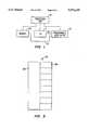
- FIG. 1is a block diagram of a digital system incorporating a programmable logic device integrated circuit
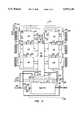
- FIG. 2is a block diagram a programmable logic device integrated circuit of the present invention
- FIG. 3is a more detailed block diagram of a logic array block of the programmable logic device integrated circuit of FIG. 2;
- FIGS. 4A-4Dare block diagrams showing four types of connections between a logic element and a memory block and a programmable interconnect array and a memory block in a programmable logic device integrated circuit;
- FIG. 5is a more detailed block diagram of the memory block of the programmable logic device integrated circuit of FIG. 2;
- FIG. 6is a block diagram of a further embodiment of the programmable logic device integrated circuit of the present invention, where the memory block has programmably selectable word size and depth size;
- FIG. 7is a more detailed block diagram of the memory block of FIG. 6.
- FIG. 1shows a block diagram of a digital system within which the present invention may be embodied.
- a processing unit 101is coupled to a memory 105, an I/O 111, and a programmable logic device (PLD) 121.
- PLD 121is coupled to memory 105 through connection 131 and to I/O 111 through connection 135.
- the systemmay be a programmed digital computer system, digital signal processing system, specialized digital switching network, or other processing system.
- the systemmay be a general purpose computer, a special purpose computer optimized for an application-specific task such as programming PLD 121, or a combination of a general purpose computer and auxiliary special purpose hardware.
- Processing unit 101may direct data to an appropriate system component for processing or storage, execute a program stored in memory 105 or input using I/O 111, or other similar function.
- Processing unit 101may be a central processing unit (CPU), microprocessor, floating point coprocessor, graphics coprocessor, hardware controller, microcontroller, programmable logic device programmed for use as a controller, or other processing unit. In some embodiments, processing unit 101 may even be a computer system.
- source codemay be stored in memory 105, compiled into machine language, and executed by processing unit 101.
- only the machine language representation of the source code, without the source code,may be stored in memory 105 for execution by processing unit 101.
- Memory 105may be a random access memory (RAM), read only memory (ROM), fixed or flexible disk media, PC Card flash disk memory, tape, or any other storage retrieval means, or any combination of these storage retrieval means.
- Processing unit 101uses I/O 111 to provide an input and output path for user interaction.
- I/O 111may be a keyboard, mouse, track ball, digitizing tablet, text or graphical display, touch screen, pen tablet, printer, or other input or output means, or any combination of these means.
- I/O 111includes a printer used for printing a hard copy of any processing unit 101 output.
- a usermay print a copy of a document prepared using a word processing program executed using processing unit 101.
- a usermay print out a copy of the source code or a listing of the logical functions contained within PLD 121.
- PLDmay serve many different purposes within the system in FIG. 1.
- PLD 121may be a logical building block of programmed digital computer 101, supporting its internal and external operations. PLD 121 is programmed to implement the logical functions necessary to carry on its particular role in system operation.
- programmed digital computer 101may use PLD 121, through connection 131, to decode memory or port addresses for accessing memory 105 or I/O 111.
- PLD 121may be programmed to store data like a memory or specialized memory, where this comes from processing unit 101 or memory 105 (via connection 131).
- PLD 121may be used as a microcontroller for a memory 105 device such as a fixed or flexible disk drive.
- PLD 121may also be configured to be a microcontroller for an I/O 111 device such as a keyboard or scanner, passing data through connection 135.
- PLD 121may be used as a controller or specialized processing unit such as a coprocessor for performing mathematical or graphical calculations.
- processing unit 101would direct data to PLD 121; PLD 121 processes this data; then PLD 121 returns the results to processing unit 101.
- processing unit 101may pass or direct a program stored in memory 105 or input using I/O 111 to PLD 121 for execution. These are some of multitude of uses of PLD 121 within a digital system.
- a systemsuch as the one shown in FIG. 1 may embody a plurality of PLDs 121, each performing different system functions.
- the system shown in FIG. 1may also be used for programming PLD 121 with a particular logic pattern.
- a computer program for designing functions into a PLDmay be stored in memory 105 and executed using processing unit 101. Then, a design characteristic which is to be programmed into PLD 121 is input via I/O 111 and processed by processing unit 101. In the end, processing unit 101 transfers and programs the design characteristic into PLD 121.
- processing unit 101is shown directly coupled to PLD 121.
- a PLD interfacemay be coupled between processing unit 101 and PLD 121.
- the PLD interfacewould provide the proper adapters or sockets for interfacing PLD 121 to processing unit 101.
- the PLD interfacewould provide the proper voltages and electrical characteristics for coupling PLD 121 to processing unit 101.
- FIG. 2is a block diagram of the overall internal architecture and organization of PLD 121 of FIG. 1. Many details of PLD architecture, organization, and circuit design are not necessary for an understanding of the present invention and such details are not shown in FIG. 2.
- PLD 121includes, among other components, an array of logic array blocks (LABs) 201, a programmable interconnect array (PIA) 203, a memory block 250 (shown in a dashed box), input-output blocks 205, and input-output pads 209.
- LABslogic array blocks
- POAprogrammable interconnect array
- PLD 121includes a two-dimensional array of LABs 201, arranged in two columns of three LABs 201 for a total of six LABs.
- LAB 201is a physically grouped set of logical resources that is configured or programmed to perform logical functions.
- the internal architecture of a LABwill be described in more detail below in connection with FIG. 3.
- PLDsmay contain any arbitrary number of LABs, more or less than PLD 121 shown in FIG. 2. Generally, in the future, as technology advances and improves, programmable logic devices with even greater numbers of LABs will undoubtedly be created.
- LABs 201need not be organized as shown in FIG. 2; for example, the array may be organized in a five-by-seven or a twenty-by-seventy matrix of LABs.
- LABs 201are connected to PIA 203 through inputs 211 and outputs 213.
- PIA 203is a global interconnect array that facilitates the combination of multiple LABs 201 to form more complex, larger logic functions than can be realized using a single LAB 201.
- a very simplified view of PIA 203is provided in dashed box 238.
- PIA 203is a two-dimensional array of conductors for routing signals between different LABs 201.
- a plurality of horizontal conductors 244extends in a first direction, coupling to inputs 211 and outputs 213 of LABs 201.
- a plurality of vertical conductors 240extends in a second direction, spanning the length of the PLD. The horizontal and vertical conductors are programmably connectable at intersections 242 of these conductors.
- PIA 203may be implemented using many memory technologies. PIA may be constructed from programmable technologies such as, among others, dynamic random access memory (DRAM), static random access memory (SRAM), erasable read only memory (EPROM), fuses, and antifuses. In a specific embodiment, PIA 203 is implemented using electrically erasable programmable read only memory (EEPROM) cells.
- DRAMdynamic random access memory
- SRAMstatic random access memory
- EPROMerasable read only memory
- fusesfuses
- antifusesantifuses
- PIA 203is implemented using electrically erasable programmable read only memory (EEPROM) cells.
- EEPROMelectrically erasable programmable read only memory
- FIG. 3shows a simplified block diagram of LAB 201 of FIG. 2.
- LAB 201is comprised of a varying number of logic elements (LEs) 300, sometimes referred to as "logic cells," and a local (or internal) interconnect structure 310.
- LEslogic elements
- LAB 201has eight LEs 300, but LAB 201 may have any number of LEs, more or less than eight.
- LAB 200has two "banks" of eight LEs for a total of sixteen LEs, where each bank has separate inputs, outputs, control signals, and carry chains.
- LE 300is the smallest logical building block of a PLD. Signals external to the LAB, such as from PIA 203 are programmably connected to LE 300 through local interconnect structure 310, although LE 300 may be implemented in many architectures other than those shown in FIGS. 2-3.
- LE 300 of the present inventionincorporates a logical function generator that is configurable to provide a logical function of a number of variables, such a four-variable boolean operation. As well as combinatorial functions, LE 300 also provides support for sequential and registered functions using, for example, D flip-flops.
- LE 300provides combinatorial and registered outputs that are connectable to PIA 203 and input-output blocks 205, outside LAB 201. Furthermore, in one embodiment, the outputs from LE 300 may be internally fed back into local interconnect structure 310; through local interconnect structure 310, an output from one LE 300 may be programmably connected to the inputs of other LEs 300, without using the global interconnect structure, PIA 203.
- Local interconnect structure 310allows short-distance interconnection of LEs, without utilizing the limited global resources, PIA 203. Through local interconnect structure 310 and local feedback, LEs 300 are programmably connectable to form larger, more complex logical functions than can be realized using a single LE 300. Furthermore, because of its reduced size and shorter length, local interconnect structure 310 has reduced parasitics compared to the global interconnection structure. Consequently, local interconnect structure 310 generally allows signals to propagate faster than through the global interconnect structure.
- global clock signal 217connects to LABs 201 to allow synchronous and sequential logic operations such as latches, registers, and counters. External, off-chip circuitry may be used to drive the global clock signal 217. Furthermore, a global clear signal 223 connects to LABs 201 to clear latches and registers within LABs 201. External, off-chip circuitry may be used to drive the global clear signal 223.
- LABs 201may output to PIA 203 through connections 213.
- Connections 213form a feedback loop from the LAB outputs back into PIA 203 to allow signals one LAB 201 to be passed to the same LAB or other LABs 201. This feedback loop uses PIA 203 resources.
- LABs 201may also output via connections 215 to input-output block 205.
- Input-output blocks 205contain circuitry facilitating the connection of outputs 215 from LABs 201 to input-output pads 209 of the PLD. Through input-output blocks 205 and input-output pads 209, output signals from LABs 201 may be interfaced to external, off-chip circuitry. Furthermore, other internal PLD signals may be connected to external, off-chip circuitry by passing them through a LAB 201.
- Input-output blocks 205also feedback outputs 215 of LABs 201 to PIA 203 through connections 220. This allows the output 215 of one LAB 201 to be coupled, via PIA 203, to itself or another LAB 201 in the PLD. Multiple LABs 201 may also be combined in this fashion.
- input-output blocks 205also have an output enable function, where the outputs at input-output pads 209 are enabled or disabled (or tristate).
- Output enable signals 219 and 221are global signals, coupled to input-output block 205, for controlling whether specific outputs are enabled or disabled.
- Input-output block 205are programmable to determine which input-outputs pads 209 are controlled (enabled or disabled) by which particular output enable signal, 209 or 221.
- input-output blocks 205are also programmably selectable to facilitate the passage of external, off-chip signals to circuitry internal to PLD 121.
- input-output blocks 205act as input buffers, taking signals from input-output pads 209 and passing them to PIA 203 through connections 220. From PIA 203, these input signals can be programmably connected to LABs 201. In typical use, a portion of input-output pads 209 will be configured for use for input purposes and a portion will be configured for output purposes.
- Memory block 250includes RAM/FIFO block 252.
- RAM/FIFO 252is a memory and associated logic for storing and retrieving data.
- RAM/FIFO 252is programmably configurable to operate as a random access memory (RAM) in a RAM mode and first-in, first out (FIFO) memory in a FIFO mode.
- RAMrandom access memory
- FIFOfirst-in, first out
- dataare stored in RAM/FIFO 252 in either a directly addressable RAM organization or FIFO memory organization.
- RAM modedata are stored and retrieved by directly addressing specific locations in the memory.
- FIFO modedata are stored in and retrieved from the RAM in a first-in, first-out fashion.
- PLD 121is programmably configurable to include a RAM or FIFO memory and can perform logical function using these types of memories. A more detailed description of RAM/FIFO 252 is given below in the discussion of FIG. 5.
- Multiplexer 255programmably selects from a data input to RAM/FIFO 252. Programmable selection of multiplexer 255 is controlled by way of user-programmable memory bits (not shown) such as EEPROM cells. Depending on the state of such user-programmed bits, an appropriate data input to RAM/FIFO 252 is selected. Multiplexer 255 has three sources of input, PIA 203, dedicated input pins 269, and output data from RAM/FIFO 252. Depending on the state of the user-programmed bits, one of these inputs is transferred through multiplexer 255 via bus 263 to RAM/FIFO 252.
- PIA 203may be programmably coupled through bus 257 to RAM/FIFO 252. Through this data path, LABs 201 and signals programmably connectable to PIA 203 may store data into RAM/FIFO 252. Through multiplexer 255 and dedicated inputs 269, external off-chip circuitry may also load RAM/FIFO 252 with data. Furthermore, the data output 261 of RAM/FIFO 252 may also be programmably selected as the data input for RAM/FIFO 252.
- RAM/FIFO 252also has a data output 262 which is connected to PIA 203.
- data stored in RAM/FIFO 252may be used by other components within PLD 121, including LABs 201.
- a sequential state machinecan be designed using LABs 201 and RAM/FIFO 252. Based on its inputs, LABs 201 determine the current state of the state machine and provide RAM/FIFO 252 with the proper memory address for this state. Based on this address, RAM/FIFO 252 provides the boolean outputs for this particular state, as well as pointers to the next possible states in the state machine. LABs 201 use these pointers, accessible via RAM/FIFO data output 262, and determines the next state for the state machine.
- Data output from RAM/FIFO 252is also programmably connectable to external, off-chip circuitry via output 261.
- Off-chip circuitrycan use this RAM/FIFO 252 output data for performing off-chip logical functions.
- output 261may be tristated, based on global output enable signals 219 and 221 (described below). When enabled, output data is produced at output 261. When disabled, output data is not produced at output 261; instead, output 261 will be in a high-impedance state. This feature allows output 261 to be connected to a bidirectional bus, such as a microprocessor's input and output lines.
- RAM/FIFO 252also has a memory address input 265.
- Multiplexer 253programmably selects a memory address from either PIA 203 or dedicated inputs 269 to transfer to memory address input 255. Programmable selection of multiplexer 253 is controlled by way of user-programmable memory bits (not shown) such as EEPROM cells.
- PIA 203is connected through bus 272 and multiplexer 253 to RAM/FIFO 252. Through this connection to PIA 203, signals programmably connectable to PIA 203 may provide memory addresses for RAM/FIFO 252.
- LABs 201may be coupled through PIA 203 and multiplexer 253 to RAM/FIFO 252. Through this data path, LABs 201 may provide memory addresses for RAM/FIFO 252.
- multiplexer 253allows external off-chip circuitry to provide memory addresses for RAM/FIFO 252.
- PIA 203connects to a control signal input 259 of RAM/FIFO 252.
- control signal input 259may be directly connected to a LAB 201 or an LE 300. Further discussion of the various types of connections for control signal input 259 of the present invention accompanies the disccussion of FIGS. 4A-4D.
- Control signal input 259governs the reading, writing, clocking, clearing, and other similar operations of RAM/FIFO 252.
- Control signal input 259may contain a plurality of control signals. In one embodiment, control signal input 259 includes five control signals, described further below.
- LABs 201are programmable connectable to control signal input 259 to direct RAM/FIFO 252 operations. For example, one LAB 201 may be configured to enable writing of data into RAM/FIFO 252 upon the occurrence of certain logic conditions. A more detailed description of control signal input 259 accompanies the discussion of FIG. 5 below.
- RAM/FIFO 252generates flag signal 276, which is connected to PIA 203.
- RAM/FIFO 252uses flag signal 276 to provide status information of RAM/FIFO 252 for other components within PLD 121.
- flag signal 276may indicate whether RAM/FIFO 252 is full, which means that no memory locations are available for storing data.
- This flag signal 276may be connected through PIA 203 to a LAB 201, which will disable writing of data into RAM/FIFO 252 when RAM/FIFO 252 is full.
- Flag signal 276may be a plurality of flag signals. In one embodiment, there are four flag signals. A more detailed description of these flag signals accompanies the discussion of FIG. 5 below.
- Global clock signal 217is global signal which is programmably connected to LABs 201 as well as RAM/FIFO 252.
- global clock signal 217may be used to synchronize particular LABs 201 and RAM/FIFO 252 operations.
- External, off-chip circuitrymay be programmably selected to control the clocking of RAM/FIFO 252 through dedicated clock inputs MEMCLK0 275 and MEMCLK1 277. A further discussion of the clocking of RAM/FIFO 252 is given below.
- Two global output enable signals, 219 and 221,are coupled to RAM/FIFO 252 and control whether output 261 is tristated or enabled. As discussed previously, global output enable signals 219 and 221 are also coupled to input-output blocks 205 for controlling the output enable feature of these blocks.
- FIGS. 4A-4Dare block diagrams of various types of connections or connection paths between LE 300 and RAM/FIFO 252 and PIA 203 and RAM/FIFO 252.
- an LE 300 of a LAB 201is programmably connectable to the control (259), data (263), or address (265) inputs of RAM/FIFO 252.
- One advantage of this connection pathis that directly connecting LE 300 to RAM/FIFO 252 bypasses PIA 203, thus avoiding PIA-associated delays.
- signals from PIA 203 of PLD 121are programmably connectable to the control (259), data (263), or address (265) inputs of RAM/FIFO 252.
- PIA 203has vertical conductors 240 and horizontal conductors 242. Vertical and horizontal conductors are programmably connectable at intersections 244 of these two conductors.
- connections 410are from a fully populated multiplexer, which means that every signal (vertical conductor) in PIA 303 is connectable to horizontal conductor 244 to control inputs to RAM/FIFO 252.
- a LAB 201may be programmably connected through PIA 203 to control (259), data (263), and address (265) inputs to RAM/FIFO 252.
- an output 213 of LAB 201is programmably coupled to a vertical conductor 240 of PIA 203.
- This vertical conductor 240is programmably coupled at intersection 242 to a vertical conductor 244 to control (259), data (263), and address (265) lines of RAM/FIFO 252.
- FIG. 4CThe embodiment shown in FIG. 4C is similar to that shown in FIG. 4B.
- a differenceis there is a partially populated multiplexer 420 for connecting vertical conductors 240 of PIA 203 to horizontal conductors 242.
- Partially populated multiplexer 420only allows selected vertical conductors 410 in PIA 203 to be programmably coupled to RAM/FIFO 252.
- RAM/FIFO 252For example, in one embodiment, only a selection three of the vertical conductors 410 may be programmably coupled to connections 405.
- Partially populated multiplexingrequired fewer programmable connections than fully populated multiplexing. Therefore, partially populated multiplexing results in reduced integrated circuit die sizes.
- FIG. 4Dhas similarities to FIG. 4C.
- a partially populated multiplexer 430programmably connects vertical conductors 240 of PIA 203 to a full crossbar switch 450.
- Crossbar switch 450is a switch that programmably connects one of its inputs, horizontal conductors 244, to one of the control (259), data (263), and address (265) lines of RAM/FIFO 252.
- Crossbar switchgives greater flexibility in permitting a horizontal conductor 244 to programmably connect to many different RAM/FIFO 252 inputs.
- FIG. 5is a more detailed block diagram of RAM/FIFO 252 of FIG. 2.
- RAM/FIFO 252includes a RAM 501, which is a random access memory for storing data.
- RAM 501may be contained in separate components.
- Many technologiescan be used for the RAM cells including, among others, dynamic- and static-type memory cells such as DRAM, SRAM, EPROM, and EEPROM.
- RAM 501is organized as an array of SRAM cells arranged 1024-words deep by 10-bits wide.
- RAM/FIFO 252can be configured to operate as a RAM or a FIFO.
- RAM modedata are stored in or retrieved from RAM 501 by direct addressing.
- FIFO modedata are stored in and retrieved from RAM 501 in a first-in, first-out manner.
- Multiplexers 575 and 577programmably select whether RAM/FIFO 252 is operating in RAM or FIFO mode. Programmable selection of multiplexers 575 and 577 are controlled by way of user-programmable memory bits (not shown) such as EEPROM cells.
- Multiplexer 575selectively couples either address bus 265 (also shown in FIG. 2) or an output 571 of a write pointer latch 505 to a write address bus 531 of RAM 501.
- Multiplexer 577selectively couples either address bus 265 or an output 573 of a read pointer latch 503 to a read address bus 533 of RAM 501.
- Write address bus 531selects an address where input data 525 is written into RAM 501.
- Read address bus 533selects an address where data is output from RAM 501.
- RAM operationis enabled when multiplexer 575 couples address bus 261 to write address bus 531 and multiplexer 577 couples address bus 261 to read address bus 533.
- direct memory addressingvia address bus 265, is used to determine the memory location where data are stored and retrieved. For example, an address is provided onto both write address bus 531 and read address bus 533 of RAM 501. Data may be read and written to the address location provided to RAM 501.
- FIFO operationis enabled when multiplexer 575 selectively couples write pointer 505 to write address bus 531 and multiplexer 577 selectively couples read pointer 503 to read address bus 533.
- addresses for reading (or retrieving) dataare provided by read pointer 503 and addresses for writing (or storing) data are provided by write pointer 505.
- Read pointer 503 and write pointer 505are latches, or registers in other embodiments, for holding the memory addresses for the reading and writing of data. Read pointer 503 and write pointer 505 are updated with new addresses after store or retrieve operations.
- a write control block 507is coupled to write pointer 505 and a read control block 513 is coupled to read pointer 503.
- Write control block 507controls the operation of write pointer 505 via control line 557.
- Read control block 513controls the operation of read pointer 503 via control line 537.
- write and read control logic blocks 507 and 513implement a FIFO memory organization by determining and updating the addresses in read pointer 503 and write pointer 507 each time data is stored or retrieved. For example, read pointer 503 points to a particular address location in RAM 501. After an item is retrieved from RAM 501, this item is no longer supposed to be in the FIFO.
- read pointer 503is incremented (or decremented in other embodiments) to the next address location holding valid data.
- write pointer 507is similarly incremented or decremented to the next open address location in RAM 501.
- signals 537 and 557are coupled to RAM 501 and are used as a write strobe for RAM 501.
- Dataare stored into RAM 501 using input bus 263 of FIG. 2. From input bus 263, data are first stored into an input latch 509, which is coupled to input bus 525 of RAM 501. Then, input latch 509 is clocked and data may be written into RAM 501. Input latch 509 may be programmed to operate in one of five clocking modes: leading-edge-triggered register, trailing-edge-triggered register, active-high latch, active-low latch, or as a direct combinatorial bypass. This feature allows more flexibility in how data is input into RAM 501.
- input latch 509In leading-edge-triggered register mode, input latch 509 will function as a register, which will be responsive to a leading edge of a clock input. In trailing-edge-triggered register mode, input latch 509 will function as a register, which will be responsive to a falling edge of a clock input. In active-high latch mode, latch 509 will function as a latch, latching data which its clock input is a high. In active-low latch mode, latch 509 will function as a latch, latching data when its clock input is a low. In direct combinatorial bypass mode, latch 509 will pass data through without any clocking; in this mode, latch 509 becomes transparent.
- output latch 515In both FIFO and RAM modes, data is clocked out of RAM 501 through output latch 515, which is coupled to output bus 527 of RAM 501.
- Output latch 515is also programmable to operate in one of the five clocking modes described above for input latch 509.
- Output latch 515outputs data to output bus 262, which is coupled to PIA 203, as shown in FIG. 2.
- output latch 515is also coupled to output bus 261 through tristate buffer 579. When tristate buffer 579 is enabled, output data from latch 515 can be transferred onto output bus 261. In the alternative, when tristate buffer 579 is disabled, output bus 261 will be in a high-impedance state (tristate).
- Multiplexer 541programmably selects the output enable control signal 542 coupled to tristate buffer 579. Programmable selection of multiplexer 541 is controlled by way of user-programmable memory bits such as EEPROM cells. Multiplexer 541 can permanently enable or disable output 261 by connecting the output enable input 542 of tristate buffer 579 to ground or VCC, respectively. Furthermore, output enable 542 can be driven by global output enable signals 219 or 221.
- Multiplexer 519programmably selects a clock signal 521 for input latch 509 and write logic 507. Programmable selection of multiplexer 519 is controlled by way of user-programmable memory bits such as EEPROM cells. Multiplexer 519 can programmably select MEMCLK1 277, global clock 217, or a signal 547 from PIA 203 as clock signal 521. MEMCLK1 277 and global clock 217 were described earlier. As for signal 547, a signal programmably connectable to PIA 203 may used to generate signal 547. For example, via PIA 203, a LAB 201 may be used to generate signal 547.
- Multiplexer 539programmably selects as a clock signal 543 for output latch 515 and read control logic 513. Programmable selection of multiplexer 539 is controlled by way of user-programmable memory bits such as EEPROM cells. Multiplexer 519 can programmably select MEMCLK0 275, global clock 217, or a signal 553 from PIA 203. MEMCLK0 275 and global clock 217 were described earlier. As for signal 553, a signal programmably connectable to PIA 203 may used to generate signal 553. For example, via PIA 203, a LAB 201 may be used to generate signal 553.
- Clocking signals 521 and 543are used to clock data into input latch 509 and output latch 515, respectively.
- Clock signals 512are also used to synchronize write control logic 507 and read control logic 513 to the clocking input latch 509 and output latch 515, respectively.
- control inputscontrol the operation of RAM/FIFO 252. These five control inputs are enable write (ENW) 549, enable read (ENR) 535, clear (CLR) 551, write clock (CKW) 521, and read clock (CKR) 543.
- CKW 521 and CKR 543are the clock signals generated by multiplexer 519 and multiplexer 539, respectively, which were described above.
- ENW 549is coupled to write control logic 507 and comes from PIA 203 (shown as control signal 259 in FIG. 2).
- a signal programmably connectable to PIA 203may generate ENW 549.
- a LAB 201may generate ENW 549.
- ENW 549enables the writing of data into RAM 501.
- ENW 549causes write control logic 507 to update write pointer 505 to the next memory location to be written in RAM 501 at the proper clock cycle of clock signal 521.
- ENR 555is coupled to read control logic 513 and comes from PIA 203 (shown as control signal 259 in FIG. 2).
- a signal programmably connectable to PIA 203may generate ENR 555.
- a LAB 201may generate ENR 555.
- ENR 555enables the reading of data from RAM 501.
- ENR 555causes read control logic 513 to update read pointer 503 to the next memory location to be read at the proper cycle of clocking signal 543.
- CLR 551is coupled to reset logic block 517 and comes from PIA 203 (shown as control signal 259 in FIG. 2). Any signal programmably connectable to PIA 203 may generate CLR 551. For example, a LAB 201 may generate CLR 551.
- Reset logic 517is coupled (not shown) to write pointer 505, write control logic 507, read pointer 503, and read control logic 513. Responsive to CLR 551, reset logic 517 resets and clears the FIFO control blocks and pointers. In one embodiment, upon powering up of the PLD integrated circuit, reset logic 517 provides a power-on reset of FIFO control blocks and pointers.
- RAM/FIFO 252has a flag logic block 511 which produces flags that provide status information for the PLD. Flags have two states, true or false. A flag is true when the status condition they represent occurs, otherwise a flag will be false. In one embodiment, flag logic block 511 generates flag signals to indicate the status of the FIFO during FIFO mode. As shown in FIG. 5, flag logic block 511 takes inputs from read pointer 503 and write pointer 523 to determine the status of the FIFO. There can be any number of flags. In the embodiment of FIG. 5, there are four flags, full flag 561, almost full flag 563, almost empty flag 565, and empty flag 567.
- Full flag 561is true when the FIFO is full, which occurs when RAM 501 has no empty memory locations available for storing data.
- Almost full flag 563is true when RAM 501 has only a specified number of empty memory locations available for data storage. The specified number is user selected by programming memory cells with this number.
- Empty flag 567is true when the FIFO is empty, which occurs when RAM 501 has no data stored.
- Almost empty flag 565is true when RAM 501 has only a specified number of memory locations already filled with data. The specified number is user selected by programming memory cells with this number. All flag signals are routed to PIA 203 of FIG. 2 (shown as connection 276), so they may be connected to LABs 201 to drive the PLD's logic functions. Flag signals may also be routed to any input-output pad 209 through PIA 203 and a LAB 201.
- FIG. 6is a block diagram of a more elaborate embodiment of PLD 121 of FIG. 2. There are many similarities between FIG. 2 and FIG. 6. Like numbered references in FIG. 2 are similar to like numbered references in FIG. 2. The following will only discuss the differences between FIG. 6 and FIG. 2.
- PLD 121includes a memory block 650, which is configurable as either a RAM or FIFO memory, as in FIG. 2.
- memory block 650can be organized, in various word size and depth size formats.
- the organization of memory block 650is programmably selectable using user-programmable memory bits (not shown) such as EEPROM cells.
- memory block 650can be organized in either a 512-word by 20-bit format or a 1024-word by 10-bit format. This feature allows greater flexibility in the design of logical functions. Some designs require a longer word size, while others require a greater number of words. Some logical functions which would have required two PLDs can be performed in one PLD of FIG. 6. Therefore, more logical functions can be implemented within a single PLD.
- Memory block 650contains RAM/FIFO block 601, a memory where data are stored for RAM or FIFO operations.
- RAM/FIFO block 601is similar to RAM/FIFO block 251 and will be described further below in the discussion of FIG. 7.
- Data inputs (625 and 627) and data outputs (685 and 687) to RAM/FIFO 601are split in two halves, each half representing half of a maximum memory word size.
- inputs 625 and 627 and outputs 685 and 687would contain ten bits.
- the word sizewill be selectable between ten bits and twenty bits.
- bits in a memory wordmay be apportioned among different buses in any proportion. For example, one bus may be five bits wide and another may be fifteen bits wide. The maximum word size of the two buses would be twenty bits.
- RAM/FIFO 601Data is input to RAM/FIFO 601 comes from several sources, programmably selectable by multiplexers 605 and 607. These sources are PIA 203 via bus 623, input-output pad 617, and input-output pad 619. In one embodiment, programmable selection of multiplexers 605 and 607 is controlled by memory cells such as EEPROM bits. External, off-chip input data can be stored into RAM/FIFO 601 using input-output pads 617 and 619. Input-output pad 617 may input data to RAM/FIFO 601 through both multiplexers 605 and 607. And input-output pad 619 may input data to RAM/FIFO 601 through both multiplexers 605 and 607. In typical operation, one input-output pad (e.g., 617) may be used for input to RAM/FIFO 601 and the other (e.g., 619) may be used for output, or vice versa.
- sourcesare PIA 203 via bus 623, input-output pad 617
- PIA 203is connected through connections 621 and 623 and multiplexers 605 and 607, respectively, to RAM/FIFO 601. Using these connections to PIA 203, signals programmably connectable to PIA 203 may be input into RAM/FIFO 601. For example, LABs 201 may be coupled through PIA 203 to RAM/FIFO 601. Through this data path, LABs 201 may store data into RAM/FIFO 601.
- RAM/FIFO 601has several data output paths. Data output is coupled to PIA 203 through buses 629 and 630, each bus containing a portion of the maximum memory word size. Through this path, data stored in RAM/FIFO 252 may be used by other components programmably connectable to PIA 203 within PLD 121, including LABs 201.
- Datamay also be output through data outputs 685 and 687.
- Data output 685outputs a portion of bits comprising the maximum word width and data output 687 outputs the remaining portion.
- Data output 685 of RAM/FIFO 601is coupled to input-output pad 619 through tristate buffer 615.
- Tristate buffer 615controls whether input-output pad 619 is enabled or disabled. When tristate buffer 615 is enabled, data output 685 is passed to input-output pad 619. When tristate buffer 615 is disabled, input-output pad 619 will be in a high-impedance state (tristate).
- Tristate buffer 615is controlled by one of two global output enable signals 219 and 221.
- Multiplexer 609programmably selects, controlled by an EEPROM cell, the output enable signal, 219 or 221, that controls tristate buffer 615. Through input-output pad 619, data from RAM/FIFO 601 is passed to external, off-chip circuitry.
- Tristate buffer 613controls whether input-output pad 617 is enabled or disabled. When tristate buffer 613 is enabled, data output 687 is passed to input-output pad 617. When tristate buffer 613 is disabled, input-output pad 617 will be in a high-impedance state (tristate). Tristate buffer 613 is controlled by one of two global output enable signals 219 or 221. Multiplexer 611 programmably selects, controlled by an EEPROM cell, the output enable signal, 219 or 221, that controls tristate buffer 613. Through input-output pad 617, data from RAM/FIFO 601 is passed to external, off-chip circuitry.
- Memory addresses for RAM/FIFO 601are input via memory address input bus 633.
- Multiplexer 603programmably selects a memory address from either PIA 203 or input-output pad 619 (which is also connected to multiplexers 607 and 605). Programmable selection of multiplexer 603 is controlled by way of user-programmable memory bits (not shown) such as EEPROM cells.
- PIA 203is connected through multiplexer 603 to RAM/FIFO 601. Using this connection to PIA 203, signals programmably connectable to PIA 203 may provide memory addresses for RAM/FIFO 601.
- LABs 201may be coupled through PIA 203 and multiplexer 603 to RAM/FIFO 601. In particular, through this data path, LABs 201 may provide memory addresses for RAM/FIFO 252.
- external off-chip circuitrymay provide memory addresses for RAM/FIFO 601.
- control signals from PIA 203are programmably coupled to RAM/FIFO 601. These will be discussed in more detail below in connection with FIG. 7. Also, RAM/FIFO 601 generates flag signals 276, coupled to PIA 201, to indicate the status of RAM/FIFO 601. These will also be discussed in more detail below in connection with FIG. 7.
- Clocking for RAM/FIFO 601is similar to clocking for RAM/FIFO 252 described above. There are three clock inputs to RAM/FIFO 601, global clock 217, MEMCLK0 275, MEMCLK1 277.
- FIG. 7is a more detailed block diagram of RAM/FIFO block 601 of FIG. 6,.
- the organization (word size and depth size) of RAM/FIFO 601is programmably.
- RAM/FIFO 610may be configured in either a 512-word by 20-bit format or 1024-word by 10-bit format.
- RAM/FIFO 601shares many similarities to RAM/FIFO 252 described above and shown in FIGS. 2-5.
- RAMs 701 and 702are stored in RAMs 701 and 702, which may be any size.
- RAMs 701 and 702are organized in a 512-words deep by 10-bits wide format.
- dataare stored or retrieved by direct addressing.
- FIFO memorydata are stored in and retrieved from the RAM in a first-in, first-out manner.
- Programmable multiplexers 775 and 777determine whether the RAM/FIFO block operates as a FIFO or a RAM. Programmable selection of multiplexers 775 and 777 is controlled by way of user-programmable memory bits (not shown) such as EEPROM cells. When multiplexers 775 and 777 are programmed to select input from address bus 633, RAM operation is enabled. If multiplexers 775 and 777 are programmed to select input from write pointer 705 and read pointer 703, respectively, FIFO operation is enabled. Read pointer 703 and write pointer 705 are similar to read pointer 503 and write pointer 505, respectively, described above.
- a memory addressis input via address bus 633, through multiplexers 775 and 777, to address registers 781 and 783, respectively, and then clocked onto memory address buses 782 and 783, respectively, into both RAMs 701 and 702.
- RAM modedirect memory addressing is used to determine the memory location where data are stored and retrieved.
- Write address bus 782is used for the write address while read address bus 791 is for the read address.
- Address register 781provides a write address for RAMs 701 and 709. The write address is the address location where data will be written.
- Address register 783provides a read address for RAMs 701 and 709. The read address is the address location where data will be retrieved.
- write pointer 703In FIFO mode, addressing is provided by read pointer 703 and write pointer 705.
- Write pointer 705will determine the memory address where data will be stored and read pointer 703 will determine the memory address where data will be retrieved.
- Write pointer 705is coupled to write control logic block 707.
- Read pointer 703is coupled to read control logic block 713.
- Write control logic block 707 and read control logic block 713generate control signals for write pointer 705 and read pointer 703 to implement a FIFO memory organization by determining and updating the addresses in write and read pointers 707 and 703, respectively, each time data is stored or retrieved.
- Write control logic 707is similar to write control logic 507 described above.
- Read control logic 703is similar to read control logic 503 described above.
- the address in write pointer 705transfers through multiplexer 775 into address register 781, where it may be clocked onto write address bus 782.
- the address in read pointer 703transfers through multiplexer 777 into address register 783, where it may be clocked onto read address bus 791.
- Write control logic 707is also coupled to RAM 701 and RAM 702 through connections 708 and 709.
- Read control logic block 713is also coupled to RAMs 701 and 702 through connections 795 and 797.
- Connections 708, 709, 795, and 797provide a write strobe for RAMs 701 and 702.
- RAMs 701 and 702Data are stored into RAMs 701 and 702 using input buses 625 and 627, each containing a portion of the maximum memory word. From inputs 625 and 627, data are first placed into input latches 709 and 710, respectively, which in turn are clocked (via clock 721) into RAMs 701 and 702, respectively. Input latches 625 and 627 are similar to input latch 509 of FIG. 5. described above. Furthermore, input latches 709 and 710 may be programmed to operate in one of five modes: leading-edge-triggered register, trailing-edge-triggered register, active-high latch, active-low latch, or as a direct combinatorial bypass.
- dataare retrieved from RAMs 701 and 702 by first placing the data into output latches 715 and 716, then clocking data onto output buses 629, 630, 685, and 687.
- Output latch 715outputs data to bus 630.
- Output latch 716outputs data to buses 630 and 685.
- Output latches 715 and 716are similar to output latch 515 of FIG. 5 described above.
- buses 685 and 687are routed to output enable buffers 615 and 613, respectively, which are connected to input-output pins 619 and 617, respectively. Also as shown in FIG.
- buses 629 and 630are fed back into PIA 203 for programmably coupling to other components of the PLD, thus available to drive the logic in the PLD integrated circuit.
- Outputs from output latches 716 and 715also input a multiplexer 793.
- Multiplexer 793selectively couples the output of latch 716 or 715 to bus 687.
- Address bus 633 (via connection 792) and read control logic 713 (via connection 794)are used as selection inputs for multiplexer 793. The selection of multiplexer 793 is based on the least significant bits of the address provided by address bus 633 and read control logic 713.
- Multiplexer 719programmably selects a clocking signal 721 for both input latches 709 and 710 and write control logic 707. Programmable selection of multiplexer 719 is controlled by way of user-programmable memory bits (not shown) such as EEPROM cells. Multiplexer 719 programmably selects MEMCLK1 277, global clock 217, or a signal 747 from PIA 203 as clock signal 721. MEMCLK1 277 and global clock 217 were described earlier. As for signal 747, a signal programmably connectable to PIA 203 may used to generate signal 547. For example, via PIA 203, a LAB 201 may be used to generate signal 547.
- Multiplexer 739programmably selects a clocking signal 743 for both output latches 715 and 716 and read control logic 713. Programmable selection of multiplexer 739 is controlled by way of user-programmable memory bits (not shown) such as EEPROM cells. Multiplexer 739 programmably selects MEMCLK0 275, global clock 217, or a signal 753 from PIA 203 as clock signal 743. MEMCLK0 275 and global clock 217 were described earlier. As for signal 753, a signal programmably connectable to PIA 203 may used to generate signal 753. For example, via PIA 203, a LAB 201 may be used to generate signal 753.
- Control signals 259 of FIG. 6are similar to control signals 259 of FIG. 2 described above.
- ENW 749is coupled to write control logic 707 for enabling or disabling writing of RAMs 701 and 702.
- ENR 755is coupled to read control logic 794 for enabling or disabling reading of RAMs 701 and 702.
- CKW 721provides a clock signal for input latches 709 and 710, write address register 781, and write control logic 707.
- CKR 743provides a clock signal for output latches 715 and 716, read address register 783, and read control logic 713.
- CLR 751is coupled to reset logic block 717 for controlling whether reset logic block resets and clears the FIFO control blocks and pointers.
- Reset logic 717is coupled (not shown) to write pointer 705, write control logic 707, read pointer 703, and read control logic 713. Responsive to CLR 751, reset logic 717 resets and clears the FIFO control blocks and pointers. In one embodiment, upon powering up of the PLD integrated circuit, reset logic 717 provides a power-on reset of FIFO control blocks and pointers.
- Flag logic 711generates flags indicating the status of RAM/FIFO 601. Flag logic 711 is similar to flag logic 511 of FIG. 5 described above. In the embodiment shown in FIG. 7, flag logic 711 takes input 706 from write pointer 705 and input 735 from read pointer 703. Responsive to its inputs, flag logic 711 generates four flag outputs, full flag 761, almost full flag 763, almost empty flag 765, and empty flag 767. These signals programmably couple to PIA 203, as shown by connection 276 in FIG. 6. Furthermore, these signals are analogous to the corresponding flag signal in FIG. 5 described above (i.e., full flag 561, almost full flag 563, almost empty flag 565, and empty flag 567).
Landscapes
- Physics & Mathematics (AREA)
- Mathematical Physics (AREA)
- Engineering & Computer Science (AREA)
- Computer Hardware Design (AREA)
- Computing Systems (AREA)
- General Engineering & Computer Science (AREA)
- Computer Networks & Wireless Communication (AREA)
- Logic Circuits (AREA)
Abstract
Description
The present invention relates to the field of programmable logic integrated circuits. More specifically, the present invention provides an enhanced programmable logic architecture, improving upon the composition, configuration, and arrangements of logic array blocks and logic elements and also the interconnections between these logic array blocks and logic elements.
Programmable Logic Devices (PLDs) are well known to those in the electronic art. Such programmable logic devices are commonly referred as PALs (Programmable Array Logic), PLAs (Programmable Logic Arrays), FPLAs (Field Programmable Logic Arrays), PLDs (Programmable Logic Devices), EPLDs (Erasable Programmable Logic Devices), EEPLDs (Electrically Erasable Programmable Logic Devices), LCAs (Logic Cell Arrays), FPGAs (Field Programmable Gate Arrays), and the like. Such devices are used in a wide array of applications where it is desirable to program standard, off-the-shelf devices for a specific application. Such devices include, for example, the well-known, Classic™, and MAX® 5000, and FLEX® 8000 EPLDs made by Altera Corp.
PLDs are generally known in which many logic array blocks (LABs) are provided in a two-dimensional array. Further, PLDs have an array of intersecting signal conductors for programmably selecting and conducting logic signals to, from, and between the logic array blocks. LABs contain a number of programmable logic elements (LEs) which provide relatively elementary logic functions such as NAND, NOR, and exclusive OR.
Resulting from the continued scaling and shrinking of semiconductor device geometries, which are used to form integrated circuits (also known as "chips"), integrated circuits have progressively become smaller and denser. For programmable logic, it becomes possible to put greater numbers of programmable logic elements onto one integrated circuit. Furthermore, as the number of elements increases, it becomes increasingly important to improve the techniques and architectures used for interconnecting the elements and routing signals between the logic blocks. In particular, it is important to provide enough interconnection resources between the programmable logic elements so that the capabilities of the logical elements can be fully utilized and so that complex logic functions (e.g., requiring the combination of multiple LABs and LEs) can be performed, without providing so much interconnection resources that there is a wasteful excess of this type of resource.
While such devices have met with substantial success, such devices also meet with certain limitations, especially in situations in which the provision of additional or alternative types of interconnections between the logic modules would have benefits sufficient to justify the additional circuitry and programming complexity. Such additional interconnection paths may be desirable for making frequently needed kinds of interconnections, for speeding certain kinds of interconnections, for allowing short distance connections to be made without tying up a more general-purpose interconnection resource such as long-distance interconnect. There is also a continuing demand for logic devices with larger capacity. This produces a need to implement logic functions more efficiently and to make better use of the portion of the device which is devoted to interconnecting individual logic modules.
As can be seen, an improved programmable logic array integrated circuit architecture is needed, especially an architecture providing additional possibilities for interconnections between the logic modules and improved techniques for organizing and interconnecting the programmable logic elements, including LABs and LEs.
The present invention is a programmable logic device integrated circuit incorporating a memory block. The memory block is a general-purpose memory configurable as a random access memory (RAM) or a first-in first-out (FIFO) memory. In one embodiment, the organization of memory block may have variable word size and depth size. Memory block is coupled to a programmable interconnect array. Signals from the programmable interconnect array may be programmably coupled to the data, address, and control inputs of the memory block. Data output and status flag signals from the memory block are programmably coupled to the programmable interconnect array.
In particular, the present invention is a programmable logic array integrated circuit including a first plurality of conductors, extending along a first dimension of a two-dimensional array; a second plurality of conductors, extending along a second dimension of the two-dimensional array, where the second plurality of conductors is programmably coupled to the first plurality of conductors; a plurality of logic array blocks, programmably coupled to the first plurality of conductors and second plurality of conductors; and a memory block, programmably coupled to the first plurality of conductors and the first plurality of conductors. Furthermore, the memory block is programmably configurable as a random access memory in a first mode and a first-in, first-out memory in a second mode. In a further embodiment, a word size and a depth size for the memory block are programmably selectable.
Other objects, features, and advantages of the present invention will become apparent upon consideration of the following detailed description and the accompanying drawings, in which like reference designations represent like features throughout the figures.
FIG. 1 is a block diagram of a digital system incorporating a programmable logic device integrated circuit;
FIG. 2 is a block diagram a programmable logic device integrated circuit of the present invention;
FIG. 3 is a more detailed block diagram of a logic array block of the programmable logic device integrated circuit of FIG. 2;
FIGS. 4A-4D are block diagrams showing four types of connections between a logic element and a memory block and a programmable interconnect array and a memory block in a programmable logic device integrated circuit;
FIG. 5 is a more detailed block diagram of the memory block of the programmable logic device integrated circuit of FIG. 2;
FIG. 6 is a block diagram of a further embodiment of the programmable logic device integrated circuit of the present invention, where the memory block has programmably selectable word size and depth size; and
FIG. 7 is a more detailed block diagram of the memory block of FIG. 6.
FIG. 1 shows a block diagram of a digital system within which the present invention may be embodied. In the particular embodiment of FIG. 1, aprocessing unit 101 is coupled to amemory 105, an I/O 111, and a programmable logic device (PLD) 121. PLD 121 is coupled tomemory 105 through connection 131 and to I/O 111 throughconnection 135. The system may be a programmed digital computer system, digital signal processing system, specialized digital switching network, or other processing system. Moreover, the system may be a general purpose computer, a special purpose computer optimized for an application-specific task such as programming PLD 121, or a combination of a general purpose computer and auxiliary special purpose hardware.
In one embodiment, source code may be stored inmemory 105, compiled into machine language, and executed byprocessing unit 101. In the alternative, only the machine language representation of the source code, without the source code, may be stored inmemory 105 for execution byprocessing unit 101.Memory 105 may be a random access memory (RAM), read only memory (ROM), fixed or flexible disk media, PC Card flash disk memory, tape, or any other storage retrieval means, or any combination of these storage retrieval means.
PLD may serve many different purposes within the system in FIG. 1. PLD 121 may be a logical building block of programmeddigital computer 101, supporting its internal and external operations. PLD 121 is programmed to implement the logical functions necessary to carry on its particular role in system operation.
As some examples of the multitude of uses for PLD 121, programmeddigital computer 101 may use PLD 121, through connection 131, to decode memory or port addresses for accessingmemory 105 or I/O 111. PLD 121 may be programmed to store data like a memory or specialized memory, where this comes fromprocessing unit 101 or memory 105 (via connection 131). PLD 121 may be used as a microcontroller for amemory 105 device such as a fixed or flexible disk drive. PLD 121 may also be configured to be a microcontroller for an I/O 111 device such as a keyboard or scanner, passing data throughconnection 135.
In other embodiments, PLD 121 may be used as a controller or specialized processing unit such as a coprocessor for performing mathematical or graphical calculations. For example, processingunit 101 would direct data toPLD 121;PLD 121 processes this data; thenPLD 121 returns the results toprocessing unit 101. Furthermore, processingunit 101 may pass or direct a program stored inmemory 105 or input using I/O 111 toPLD 121 for execution. These are some of multitude of uses ofPLD 121 within a digital system. Also, a system such as the one shown in FIG. 1 may embody a plurality ofPLDs 121, each performing different system functions.
The system shown in FIG. 1 may also be used forprogramming PLD 121 with a particular logic pattern. A computer program for designing functions into a PLD may be stored inmemory 105 and executed usingprocessing unit 101. Then, a design characteristic which is to be programmed intoPLD 121 is input via I/O 111 and processed by processingunit 101. In the end, processingunit 101 transfers and programs the design characteristic intoPLD 121.
In FIG. 1, processingunit 101 is shown directly coupled toPLD 121. However, in other embodiments, a PLD interface may be coupled betweenprocessing unit 101 andPLD 121. The PLD interface would provide the proper adapters or sockets for interfacingPLD 121 toprocessing unit 101. Moreover, the PLD interface would provide the proper voltages and electrical characteristics forcoupling PLD 121 toprocessing unit 101.
FIG. 2 is a block diagram of the overall internal architecture and organization ofPLD 121 of FIG. 1. Many details of PLD architecture, organization, and circuit design are not necessary for an understanding of the present invention and such details are not shown in FIG. 2.PLD 121 includes, among other components, an array of logic array blocks (LABs) 201, a programmable interconnect array (PIA) 203, a memory block 250 (shown in a dashed box), input-output blocks 205, and input-output pads 209.
In the particular embodiment shown in FIG. 2,PLD 121 includes a two-dimensional array ofLABs 201, arranged in two columns of threeLABs 201 for a total of six LABs.LAB 201 is a physically grouped set of logical resources that is configured or programmed to perform logical functions. The internal architecture of a LAB will be described in more detail below in connection with FIG. 3. PLDs may contain any arbitrary number of LABs, more or less thanPLD 121 shown in FIG. 2. Generally, in the future, as technology advances and improves, programmable logic devices with even greater numbers of LABs will undoubtedly be created. Furthermore,LABs 201 need not be organized as shown in FIG. 2; for example, the array may be organized in a five-by-seven or a twenty-by-seventy matrix of LABs.
FIG. 3 shows a simplified block diagram ofLAB 201 of FIG. 2.LAB 201 is comprised of a varying number of logic elements (LEs) 300, sometimes referred to as "logic cells," and a local (or internal)interconnect structure 310.LAB 201 has eightLEs 300, butLAB 201 may have any number of LEs, more or less than eight. In a further embodiment of the present invention, LAB 200 has two "banks" of eight LEs for a total of sixteen LEs, where each bank has separate inputs, outputs, control signals, and carry chains.
A general overview ofLE 300 is presented here, sufficient to provide a basic understanding ofLAB 201 and the present invention.LE 300 is the smallest logical building block of a PLD. Signals external to the LAB, such as fromPIA 203 are programmably connected toLE 300 throughlocal interconnect structure 310, althoughLE 300 may be implemented in many architectures other than those shown in FIGS. 2-3. In one embodiment,LE 300 of the present invention incorporates a logical function generator that is configurable to provide a logical function of a number of variables, such a four-variable boolean operation. As well as combinatorial functions,LE 300 also provides support for sequential and registered functions using, for example, D flip-flops.
Returning to FIG. 2,global clock signal 217 connects toLABs 201 to allow synchronous and sequential logic operations such as latches, registers, and counters. External, off-chip circuitry may be used to drive theglobal clock signal 217. Furthermore, a globalclear signal 223 connects toLABs 201 to clear latches and registers withinLABs 201. External, off-chip circuitry may be used to drive the globalclear signal 223.
In the embodiment shown in FIG. 2, input-output blocks 205 also have an output enable function, where the outputs at input-output pads 209 are enabled or disabled (or tristate). Output enablesignals output block 205, for controlling whether specific outputs are enabled or disabled. Input-output block 205 are programmable to determine which input-outputs pads 209 are controlled (enabled or disabled) by which particular output enable signal, 209 or 221.
Furthermore, input-output blocks 205 are also programmably selectable to facilitate the passage of external, off-chip signals to circuitry internal toPLD 121. In this configuration, input-output blocks 205 act as input buffers, taking signals from input-output pads 209 and passing them toPIA 203 throughconnections 220. FromPIA 203, these input signals can be programmably connected toLABs 201. In typical use, a portion of input-output pads 209 will be configured for use for input purposes and a portion will be configured for output purposes.
Data is input into RAM/FIFO 252 through multiplexer 255 anddata input 263. Multiplexer 255 programmably selects from a data input to RAM/FIFO 252. Programmable selection of multiplexer 255 is controlled by way of user-programmable memory bits (not shown) such as EEPROM cells. Depending on the state of such user-programmed bits, an appropriate data input to RAM/FIFO 252 is selected. Multiplexer 255 has three sources of input,PIA 203, dedicated input pins 269, and output data from RAM/FIFO 252. Depending on the state of the user-programmed bits, one of these inputs is transferred through multiplexer 255 viabus 263 to RAM/FIFO 252.PIA 203 may be programmably coupled throughbus 257 to RAM/FIFO 252. Through this data path,LABs 201 and signals programmably connectable toPIA 203 may store data into RAM/FIFO 252. Through multiplexer 255 anddedicated inputs 269, external off-chip circuitry may also load RAM/FIFO 252 with data. Furthermore, thedata output 261 of RAM/FIFO 252 may also be programmably selected as the data input for RAM/FIFO 252.
RAM/FIFO 252 also has adata output 262 which is connected toPIA 203. ThroughPIA 203, data stored in RAM/FIFO 252 may be used by other components withinPLD 121, includingLABs 201. For example, a sequential state machine can be designed usingLABs 201 and RAM/FIFO 252. Based on its inputs,LABs 201 determine the current state of the state machine and provide RAM/FIFO 252 with the proper memory address for this state. Based on this address, RAM/FIFO 252 provides the boolean outputs for this particular state, as well as pointers to the next possible states in the state machine.LABs 201 use these pointers, accessible via RAM/FIFO data output 262, and determines the next state for the state machine.
Data output from RAM/FIFO 252 is also programmably connectable to external, off-chip circuitry viaoutput 261. Off-chip circuitry can use this RAM/FIFO 252 output data for performing off-chip logical functions. Furthermore, in one embodiment,output 261 may be tristated, based on global output enablesignals 219 and 221 (described below). When enabled, output data is produced atoutput 261. When disabled, output data is not produced atoutput 261; instead,output 261 will be in a high-impedance state. This feature allowsoutput 261 to be connected to a bidirectional bus, such as a microprocessor's input and output lines.
RAM/FIFO 252 also has amemory address input 265. Multiplexer 253 programmably selects a memory address from eitherPIA 203 ordedicated inputs 269 to transfer to memory address input 255. Programmable selection of multiplexer 253 is controlled by way of user-programmable memory bits (not shown) such as EEPROM cells.PIA 203 is connected throughbus 272 and multiplexer 253 to RAM/FIFO 252. Through this connection toPIA 203, signals programmably connectable toPIA 203 may provide memory addresses for RAM/FIFO 252. For example,LABs 201 may be coupled throughPIA 203 and multiplexer 253 to RAM/FIFO 252. Through this data path,LABs 201 may provide memory addresses for RAM/FIFO 252. Alternatively, throughdedicated inputs 269, multiplexer 253 allows external off-chip circuitry to provide memory addresses for RAM/FIFO 252.
In FIG. 2,PIA 203 connects to acontrol signal input 259 of RAM/FIFO 252. In other embodiments of the present invention, controlsignal input 259 may be directly connected to aLAB 201 or anLE 300. Further discussion of the various types of connections forcontrol signal input 259 of the present invention accompanies the disccussion of FIGS. 4A-4D.Control signal input 259 governs the reading, writing, clocking, clearing, and other similar operations of RAM/FIFO 252.Control signal input 259 may contain a plurality of control signals. In one embodiment, controlsignal input 259 includes five control signals, described further below. ThroughPIA 203,LABs 201 are programmable connectable to controlsignal input 259 to direct RAM/FIFO 252 operations. For example, oneLAB 201 may be configured to enable writing of data into RAM/FIFO 252 upon the occurrence of certain logic conditions. A more detailed description ofcontrol signal input 259 accompanies the discussion of FIG. 5 below.
RAM/FIFO 252 generatesflag signal 276, which is connected toPIA 203. RAM/FIFO 252 usesflag signal 276 to provide status information of RAM/FIFO 252 for other components withinPLD 121. For example,flag signal 276 may indicate whether RAM/FIFO 252 is full, which means that no memory locations are available for storing data. Thisflag signal 276 may be connected throughPIA 203 to aLAB 201, which will disable writing of data into RAM/FIFO 252 when RAM/FIFO 252 is full.Flag signal 276 may be a plurality of flag signals. In one embodiment, there are four flag signals. A more detailed description of these flag signals accompanies the discussion of FIG. 5 below.
Three clock inputs,global clock signal 217,MEMCLK0 275, andMEMCLK1 277, may be programmably selected for controlling the clocking of data into RAM/FIFO 252.Global clock signal 217 is global signal which is programmably connected toLABs 201 as well as RAM/FIFO 252. For example,global clock signal 217 may be used to synchronizeparticular LABs 201 and RAM/FIFO 252 operations. External, off-chip circuitry may be programmably selected to control the clocking of RAM/FIFO 252 through dedicated clock inputs MEMCLK0 275 andMEMCLK1 277. A further discussion of the clocking of RAM/FIFO 252 is given below.
Two global output enable signals, 219 and 221, are coupled to RAM/FIFO 252 and control whetheroutput 261 is tristated or enabled. As discussed previously, global output enablesignals output blocks 205 for controlling the output enable feature of these blocks.
FIGS. 4A-4D are block diagrams of various types of connections or connection paths betweenLE 300 and RAM/FIFO 252 andPIA 203 and RAM/FIFO 252. In the embodiment shown in FIG. 4A, anLE 300 of aLAB 201 is programmably connectable to the control (259), data (263), or address (265) inputs of RAM/FIFO 252. There are one or more programmable direct connections 405 to control (259), data (263), and address (265) lines of RAM/FIFO 252. One advantage of this connection path is that directly connectingLE 300 to RAM/FIFO 252 bypassesPIA 203, thus avoiding PIA-associated delays.
In the embodiment shown in FIG. 4B, signals fromPIA 203 ofPLD 121 are programmably connectable to the control (259), data (263), or address (265) inputs of RAM/FIFO 252. There are one or moreprogrammable connection paths 410 fromPIA 203 to control (259), data (263), or address (265) lines of RAM/FIFO 252.PIA 203 hasvertical conductors 240 andhorizontal conductors 242. Vertical and horizontal conductors are programmably connectable atintersections 244 of these two conductors. Furthermore,connections 410 are from a fully populated multiplexer, which means that every signal (vertical conductor) in PIA 303 is connectable tohorizontal conductor 244 to control inputs to RAM/FIFO 252. For example, aLAB 201 may be programmably connected throughPIA 203 to control (259), data (263), and address (265) inputs to RAM/FIFO 252. Specifically, anoutput 213 ofLAB 201 is programmably coupled to avertical conductor 240 ofPIA 203. Thisvertical conductor 240 is programmably coupled atintersection 242 to avertical conductor 244 to control (259), data (263), and address (265) lines of RAM/FIFO 252.
The embodiment shown in FIG. 4C is similar to that shown in FIG. 4B. A difference is there is a partiallypopulated multiplexer 420 for connectingvertical conductors 240 ofPIA 203 tohorizontal conductors 242. Partiallypopulated multiplexer 420 only allows selectedvertical conductors 410 inPIA 203 to be programmably coupled to RAM/FIFO 252. For example, in one embodiment, only a selection three of thevertical conductors 410 may be programmably coupled to connections 405. Partially populated multiplexing required fewer programmable connections than fully populated multiplexing. Therefore, partially populated multiplexing results in reduced integrated circuit die sizes.
The embodiment shown in FIG. 4D has similarities to FIG. 4C. A partiallypopulated multiplexer 430 programmably connectsvertical conductors 240 ofPIA 203 to afull crossbar switch 450.Crossbar switch 450 is a switch that programmably connects one of its inputs,horizontal conductors 244, to one of the control (259), data (263), and address (265) lines of RAM/FIFO 252. Crossbar switch gives greater flexibility in permitting ahorizontal conductor 244 to programmably connect to many different RAM/FIFO 252 inputs.
FIG. 5 is a more detailed block diagram of RAM/FIFO 252 of FIG. 2. RAM/FIFO 252 includes a RAM 501, which is a random access memory for storing data. In other embodiments, RAM 501 may be contained in separate components. Many technologies can be used for the RAM cells including, among others, dynamic- and static-type memory cells such as DRAM, SRAM, EPROM, and EEPROM. In a specific embodiment, RAM 501 is organized as an array of SRAM cells arranged 1024-words deep by 10-bits wide.
As discussed above, RAM/FIFO 252 can be configured to operate as a RAM or a FIFO. In the RAM mode, data are stored in or retrieved from RAM 501 by direct addressing. In FIFO mode, data are stored in and retrieved from RAM 501 in a first-in, first-out manner.
RAM operation is enabled when multiplexer 575 couples addressbus 261 to writeaddress bus 531 and multiplexer 577 couples addressbus 261 to readaddress bus 533. In RAM mode, direct memory addressing, viaaddress bus 265, is used to determine the memory location where data are stored and retrieved. For example, an address is provided onto both writeaddress bus 531 and readaddress bus 533 of RAM 501. Data may be read and written to the address location provided to RAM 501.
FIFO operation is enabled when multiplexer 575 selectively couples write pointer 505 to writeaddress bus 531 andmultiplexer 577 selectively couples readpointer 503 to readaddress bus 533. In FIFO mode, addresses for reading (or retrieving) data are provided byread pointer 503 and addresses for writing (or storing) data are provided by write pointer 505. Readpointer 503 and write pointer 505 are latches, or registers in other embodiments, for holding the memory addresses for the reading and writing of data. Readpointer 503 and write pointer 505 are updated with new addresses after store or retrieve operations.
Awrite control block 507 is coupled to write pointer 505 and aread control block 513 is coupled to readpointer 503. Write control block 507 controls the operation of write pointer 505 viacontrol line 557. Readcontrol block 513 controls the operation ofread pointer 503 viacontrol line 537. In operation, write and read control logic blocks 507 and 513 implement a FIFO memory organization by determining and updating the addresses inread pointer 503 and writepointer 507 each time data is stored or retrieved. For example, readpointer 503 points to a particular address location in RAM 501. After an item is retrieved from RAM 501, this item is no longer supposed to be in the FIFO. To account for this, responsive to controlsignal 537, readpointer 503 is incremented (or decremented in other embodiments) to the next address location holding valid data. Similarly, after a write operation, responsive to signal 557, writepointer 507 is similarly incremented or decremented to the next open address location in RAM 501. Furthermore, signals 537 and 557 are coupled to RAM 501 and are used as a write strobe for RAM 501.
Data are stored into RAM 501 usinginput bus 263 of FIG. 2. Frominput bus 263, data are first stored into aninput latch 509, which is coupled to input bus 525 of RAM 501. Then,input latch 509 is clocked and data may be written into RAM 501.Input latch 509 may be programmed to operate in one of five clocking modes: leading-edge-triggered register, trailing-edge-triggered register, active-high latch, active-low latch, or as a direct combinatorial bypass. This feature allows more flexibility in how data is input into RAM 501.
In leading-edge-triggered register mode,input latch 509 will function as a register, which will be responsive to a leading edge of a clock input. In trailing-edge-triggered register mode,input latch 509 will function as a register, which will be responsive to a falling edge of a clock input. In active-high latch mode, latch 509 will function as a latch, latching data which its clock input is a high. In active-low latch mode, latch 509 will function as a latch, latching data when its clock input is a low. In direct combinatorial bypass mode, latch 509 will pass data through without any clocking; in this mode,latch 509 becomes transparent.
In both FIFO and RAM modes, data is clocked out of RAM 501 through output latch 515, which is coupled to output bus 527 of RAM 501. Output latch 515 is also programmable to operate in one of the five clocking modes described above forinput latch 509. Output latch 515 outputs data tooutput bus 262, which is coupled toPIA 203, as shown in FIG. 2. Furthermore, output latch 515 is also coupled tooutput bus 261 throughtristate buffer 579. Whentristate buffer 579 is enabled, output data from latch 515 can be transferred ontooutput bus 261. In the alternative, whentristate buffer 579 is disabled,output bus 261 will be in a high-impedance state (tristate).
Clocking signals 521 and 543 are used to clock data intoinput latch 509 and output latch 515, respectively. Clock signals 512 are also used to synchronizewrite control logic 507 and readcontrol logic 513 to the clockinginput latch 509 and output latch 515, respectively.
Furthermore, five control inputs control the operation of RAM/FIFO 252. These five control inputs are enable write (ENW) 549, enable read (ENR) 535, clear (CLR) 551, write clock (CKW) 521, and read clock (CKR) 543.CKW 521 andCKR 543 are the clock signals generated bymultiplexer 519 andmultiplexer 539, respectively, which were described above.
RAM/FIFO 252 has aflag logic block 511 which produces flags that provide status information for the PLD. Flags have two states, true or false. A flag is true when the status condition they represent occurs, otherwise a flag will be false. In one embodiment,flag logic block 511 generates flag signals to indicate the status of the FIFO during FIFO mode. As shown in FIG. 5,flag logic block 511 takes inputs fromread pointer 503 and write pointer 523 to determine the status of the FIFO. There can be any number of flags. In the embodiment of FIG. 5, there are four flags,full flag 561, almostfull flag 563, almostempty flag 565, andempty flag 567.
FIG. 6 is a block diagram of a more elaborate embodiment ofPLD 121 of FIG. 2. There are many similarities between FIG. 2 and FIG. 6. Like numbered references in FIG. 2 are similar to like numbered references in FIG. 2. The following will only discuss the differences between FIG. 6 and FIG. 2.
In FIG. 6,PLD 121 includes amemory block 650, which is configurable as either a RAM or FIFO memory, as in FIG. 2. However,memory block 650 can be organized, in various word size and depth size formats. The organization ofmemory block 650 is programmably selectable using user-programmable memory bits (not shown) such as EEPROM cells. In a specific embodiment,memory block 650 can be organized in either a 512-word by 20-bit format or a 1024-word by 10-bit format. This feature allows greater flexibility in the design of logical functions. Some designs require a longer word size, while others require a greater number of words. Some logical functions which would have required two PLDs can be performed in one PLD of FIG. 6. Therefore, more logical functions can be implemented within a single PLD.
Data is input to RAM/FIFO 601 comes from several sources, programmably selectable bymultiplexers PIA 203 viabus 623, input-output pad 617, and input-output pad 619. In one embodiment, programmable selection ofmultiplexers FIFO 601 using input-output pads 617 and 619. Input-output pad 617 may input data to RAM/FIFO 601 through bothmultiplexers output pad 619 may input data to RAM/FIFO 601 through bothmultiplexers FIFO 601 and the other (e.g., 619) may be used for output, or vice versa.
Furthermore,PIA 203 is connected throughconnections multiplexers FIFO 601. Using these connections toPIA 203, signals programmably connectable toPIA 203 may be input into RAM/FIFO 601. For example,LABs 201 may be coupled throughPIA 203 to RAM/FIFO 601. Through this data path,LABs 201 may store data into RAM/FIFO 601.
RAM/FIFO 601 has several data output paths. Data output is coupled toPIA 203 throughbuses FIFO 252 may be used by other components programmably connectable toPIA 203 withinPLD 121, includingLABs 201.
Data may also be output throughdata outputs Data output 685 outputs a portion of bits comprising the maximum word width anddata output 687 outputs the remaining portion.Data output 685 of RAM/FIFO 601 is coupled to input-output pad 619 through tristate buffer 615. Tristate buffer 615 controls whether input-output pad 619 is enabled or disabled. When tristate buffer 615 is enabled,data output 685 is passed to input-output pad 619. When tristate buffer 615 is disabled, input-output pad 619 will be in a high-impedance state (tristate). Tristate buffer 615 is controlled by one of two global output enablesignals Multiplexer 609 programmably selects, controlled by an EEPROM cell, the output enable signal, 219 or 221, that controls tristate buffer 615. Through input-output pad 619, data from RAM/FIFO 601 is passed to external, off-chip circuitry.
Similarly,data output 687 of RAM/FIFO 601 is coupled to input-output pad 617 throughtristate buffer 613.Tristate buffer 613 controls whether input-output pad 617 is enabled or disabled. Whentristate buffer 613 is enabled,data output 687 is passed to input-output pad 617. Whentristate buffer 613 is disabled, input-output pad 617 will be in a high-impedance state (tristate).Tristate buffer 613 is controlled by one of two global output enablesignals tristate buffer 613. Through input-output pad 617, data from RAM/FIFO 601 is passed to external, off-chip circuitry.
Memory addresses for RAM/FIFO 601 are input via memoryaddress input bus 633.Multiplexer 603 programmably selects a memory address from eitherPIA 203 or input-output pad 619 (which is also connected to multiplexers 607 and 605). Programmable selection ofmultiplexer 603 is controlled by way of user-programmable memory bits (not shown) such as EEPROM cells.PIA 203 is connected throughmultiplexer 603 to RAM/FIFO 601. Using this connection toPIA 203, signals programmably connectable toPIA 203 may provide memory addresses for RAM/FIFO 601. For example,LABs 201 may be coupled throughPIA 203 andmultiplexer 603 to RAM/FIFO 601. In particular, through this data path,LABs 201 may provide memory addresses for RAM/FIFO 252. Alternatively, viamultiplexer 603 and input-output pad 619, external off-chip circuitry may provide memory addresses for RAM/FIFO 601.
Similar to the embodiment in FIG. 2, control signals fromPIA 203 are programmably coupled to RAM/FIFO 601. These will be discussed in more detail below in connection with FIG. 7. Also, RAM/FIFO 601 generates flag signals 276, coupled toPIA 201, to indicate the status of RAM/FIFO 601. These will also be discussed in more detail below in connection with FIG. 7. Clocking for RAM/FIFO 601 is similar to clocking for RAM/FIFO 252 described above. There are three clock inputs to RAM/FIFO 601,global clock 217,MEMCLK0 275,MEMCLK1 277.
FIG. 7 is a more detailed block diagram of RAM/FIFO block 601 of FIG. 6,. The organization (word size and depth size) of RAM/FIFO 601 is programmably. In an embodiment, RAM/FIFO 610 may be configured in either a 512-word by 20-bit format or 1024-word by 10-bit format. RAM/FIFO 601 shares many similarities to RAM/FIFO 252 described above and shown in FIGS. 2-5.
Data are stored inRAMs RAMs
In FIFO mode, addressing is provided byread pointer 703 and writepointer 705. Writepointer 705 will determine the memory address where data will be stored and readpointer 703 will determine the memory address where data will be retrieved. Writepointer 705 is coupled to writecontrol logic block 707. Readpointer 703 is coupled to readcontrol logic block 713. Writecontrol logic block 707 and readcontrol logic block 713 generate control signals forwrite pointer 705 and readpointer 703 to implement a FIFO memory organization by determining and updating the addresses in write and readpointers control logic 707 is similar to writecontrol logic 507 described above. Readcontrol logic 703 is similar to readcontrol logic 503 described above. The address inwrite pointer 705 transfers through multiplexer 775 intoaddress register 781, where it may be clocked ontowrite address bus 782. The address inread pointer 703 transfers throughmultiplexer 777 intoaddress register 783, where it may be clocked onto readaddress bus 791.
Writecontrol logic 707 is also coupled toRAM 701 andRAM 702 throughconnections control logic block 713 is also coupled toRAMs connections Connections RAMs
Data are stored intoRAMs input buses inputs RAMs input latch 509 of FIG. 5. described above. Furthermore, input latches 709 and 710 may be programmed to operate in one of five modes: leading-edge-triggered register, trailing-edge-triggered register, active-high latch, active-low latch, or as a direct combinatorial bypass.
For output, data are retrieved fromRAMs output buses Output latch 715 outputs data tobus 630.Output latch 716 outputs data tobuses buses buffers 615 and 613, respectively, which are connected to input-output pins 619 and 617, respectively. Also as shown in FIG. 6,buses PIA 203 for programmably coupling to other components of the PLD, thus available to drive the logic in the PLD integrated circuit. Outputs from output latches 716 and 715 also input amultiplexer 793.Multiplexer 793 selectively couples the output oflatch bus 687. Address bus 633 (via connection 792) and read control logic 713 (via connection 794) are used as selection inputs formultiplexer 793. The selection ofmultiplexer 793 is based on the least significant bits of the address provided byaddress bus 633 and readcontrol logic 713.
As shown in FIG. 6, control signals 259 fromPIA 203 input into RAM/FIFO 601 for controlling the operation of RAM/FIFO 601. Control signals 259 of FIG. 6 are similar to controlsignals 259 of FIG. 2 described above. In the embodiment shown in FIG. 7, there are five control signal inputs: enable write (ENW) 749, enable read (ENR) 755, Clear (CLR) 751, write clock (CKW) 721, and read clock (CKR) 743. These signals are analogous tocorresponding ENW 549, ENR 535,CLR 551,CKW 521, andCKR 543 signals described above.ENW 749 is coupled to writecontrol logic 707 for enabling or disabling writing ofRAMs ENR 755 is coupled to readcontrol logic 794 for enabling or disabling reading ofRAMs CKW 721 provides a clock signal for input latches 709 and 710, writeaddress register 781, and writecontrol logic 707.CKR 743 provides a clock signal for output latches 715 and 716, readaddress register 783, and readcontrol logic 713.
The foregoing description of preferred embodiments of the invention has been presented for the purposes of illustration and description. It is not intended to be exhaustive or to limit the invention to the precise form described, and many modifications and variations are possible in light of the teaching above. The embodiments were chosen and described in order to best explain the principles of the invention and its practical applications to thereby enable others skilled in the art to best utilize the invention in various embodiments and with various modifications as are suited to the particular use contemplated. It is intended that the scope of the invention be defined by the claims appended hereto.
Claims (36)
1. A programmable logic device integrated circuit comprising:
a first plurality of conductors, extending along a first dimension of a two-dimensional array;
a second plurality of conductors, extending along a second dimension of said two-dimensional array, wherein said second plurality of conductors is programmably coupled to said first plurality of conductors;
a plurality of logic array blocks, programmably coupled to said first plurality of conductors and second plurality of conductors; and
a memory block, programmably coupled to said first plurality of conductors, wherein said memory block is programmably configurable as a random access memory in a first mode and a first-in, first-out memory in a second mode.
2. The programmable logic device integrated circuit of claim 1 wherein a word size and a depth size for said memory block are programmably selectable.
3. The programmable logic device integrated circuit of claim 1 wherein said first plurality of conductors is coupled to an address bus of said memory block.
4. The programmable logic device integrated circuit of claim 1 wherein said first plurality of conductors is coupled to a data bus of said memory block.
5. The programmable logic device integrated circuit of claim 1 wherein an output bus of said memory block is coupled to said first plurality of conductors.
6. The programmable logic device integrated circuit of claim 1 further comprising:
a global clock, coupled to said plurality of logic array blocks and said memory block.
7. The programmable logic device integrated circuit of claim 1 further comprising:
a first memory clock, coupled to said memory block; and
a second memory clock, coupled to said memory block.
8. The programmable logic device integrated circuit of claim 1 wherein said memory block further comprises a plurality of control inputs, programmably coupled to said first plurality of conductors, wherein said plurality of control inputs control operations of said memory block.
9. The programmable logic device integrated circuit of claim 1 wherein at least one logic array block of said plurality of logic array blocks is coupled directly to, without passing through said second plurality of conductors, a plurality of control inputs for said memory block.
10. The programmable logic device integrated circuit of claim 1 wherein said memory block generates a plurality of flag outputs, programmably coupled to said first plurality of conductors, wherein said plurality of flag outputs indicate a status of said memory block.
11. The programmable logic device integrated circuit of claim 1 wherein at least one logic array block of said plurality of logic array blocks is coupled directly to said memory block, without passing through said second plurality of conductors.
12. The programmable logic device integrated circuit of claim 1 wherein said second plurality of conductors is programmably coupled to said memory block through a plurality of fully populated multiplexers.
13. The programmable logic device integrated circuit of claim 1 wherein said second plurality of conductors is programmably coupled to said memory block through a plurality of partially populated multiplexers.
14. The programmable logic device integrated circuit of claim 1 further comprising:
a crossbar switch, coupled to said memory block, wherein said second plurality of conductors is programmably coupled through a plurality of partially populated multiplexers to said crossbar switch.
15. The programmable logic device integrated circuit of claim 1 further comprising:
a plurality of input-output blocks, coupled to said plurality of logic array blocks; and
an output enable signal, programmably coupled to said plurality of input-output blocks and said memory block.
16. A digital processing system comprising:
processing unit;
memory, coupled to said processing unit; and
a programmable logic device integrated circuit as recited in claim 1, coupled to said processing unit and said memory.
17. The programmable logic device integrated circuit of claim 1 further comprising:
an address bus multiplexer, wherein said address bus multiplexer selectably couples an input pad or said first plurality of conductors to an address bus of said memory block.
18. The programmable logic device integrated circuit of claim 1 further comprising:
a data bus multiplexer, wherein said data bus multiplexer selectably couples an input pad, said first plurality of conductors, or an output of said memory block to a data bus of said memory block.
19. A programmable logic device integrated circuit comprising:
a first plurality of conductors, extending along a first dimension of a two-dimensional array;
a second plurality of conductors, extending along a second dimension of said two-dimensional array, wherein said second plurality of conductors is programmably coupled to said first plurality of conductors;
a plurality of logic array blocks, programmably coupled to said first plurality of conductors and second plurality of conductors;
a memory block, programmably coupled to said first plurality of conductors; and
an address bus multiplexer, wherein said address bus multiplexer selectably couples an input pad or said first plurality of conductors to an address bus of said memory block.
20. A programmable logic device integrated circuit comprising:
a first plurality of conductors, extending along a first dimension of a two-dimensional array;
a second plurality of conductors, extending along a second dimension of said two-dimensional array, wherein said second plurality of conductors is programmably coupled to said first plurality of conductors;
a plurality of logic array blocks, programmably coupled to said first plurality of conductors and second plurality of conductors;
a memory block, programmably coupled to said first plurality of conductors; and
a data bus multiplexer, wherein said data bus multiplexer selectably couples an input pad, said first plurality of conductors, or an output of said memory block to a data bus of said memory block.
21. A programmable logic device integrated circuit comprising:
a first plurality of conductors, extending along a first dimension of a two-dimensional array;
a second plurality of conductors, extending along a second dimension of said two-dimensional array, wherein said second plurality of conductors is programmably coupled to said first plurality of conductors;
a plurality of logic array blocks, programmably coupled to said first plurality of conductors and second plurality of conductors;
a memory block, programmably coupled to said first plurality of conductors, wherein said memory block is programmably configurable as a random access memory in a first mode and a first-in, first-out memory in a second mode, wherein said memory block further comprises a plurality of control inputs programmably coupled to said first plurality of conductors, wherein said plurality of control inputs control operations of said memory block, wherein said memory block generates a plurality of flag outputs programmably coupled to said first plurality of conductors, wherein said plurality of flag outputs indicate a status of said memory block;
an address bus multiplexer, wherein said multiplexer selectably couples an input pad or said first plurality of conductors to an address bus of said memory block; and
a data bus multiplexer, wherein said multiplexer selectably couples said input pad, said first plurality of conductors, or an output of said memory block to a data bus of said memory block.
22. The programmable logic device integrated circuit of claim 21 wherein a word size and a depth size for said memory block are programmably selectable.
23. A memory block for a programmable logic device comprising:
at least one random access memory;
a read pointer latch;
a write pointer latch;
a read address multiplexer, coupled to a read address input of said at least one random access memory, wherein said read address multiplexer programmably couples said read pointer latch to a read address input of said at least one random access memory; and
a write address multiplexer, coupled to a write address input of said at least one random access memory, wherein said write address multiplexer programmably couples said write pointer latch to a write address input of said at least one random access memory.
24. The memory block of claim 23 wherein said read address multiplexer programmably couples a programmable interconnect array of said programmable logic device to said read address input of said at least one random access memory.
25. The memory block of claim 23 wherein said write address multiplexer programmably couples a programmable interconnect array of said programmable logic device to said write address input of said at least one random access memory.
26. The memory block of claim 23 further comprising:
a read control block, coupled to said read pointer latch; and
a write control block, coupled to said write pointer latch.
27. The memory block of claims 23 or 26 further comprising:
an input latch, wherein an output of said input latch is coupled to a data input of said at least one random access memory; and
an output latch, wherein an input of said output latch is coupled to a data output of said at least one random access memory.
28. The memory block of claim 27 wherein said input latch is programmably configurable as a leading-edge-triggered register.
29. The memory block of claim 27 wherein said input latch is programmably configurable as an active-low latch.
30. The memory block of claim 27 wherein said input latch is programmably configurable as a direct combinatorial bypass.
31. The memory block of claim 27 further comprising:
a first clock signal, coupled to said input latch and said read control block; and
a second clock signal, coupled to said output latch and said write control block.
32. The memory block of claim 23 further comprising:
a tristate buffer, coupled to an output of said output latch, wherein said output of said output latch is programmably coupled to a programmable interconnect array of said programmable logic device, wherein an output of said tristate buffer is coupled to an input-output pad of said programmable logic device.
33. The memory block of claim 23 further comprising:
a flag logic block, coupled to said write pointer latch, wherein said flag logic block generates a plurality of flag outputs, wherein said plurality of flag outputs is programmably coupled to a programmable interconnect array of said programmable logic device.
34. The memory block of claim 23 further comprising:
a reset logic block, coupled to said write pointer latch and said read pointer latch, wherein said reset logic block resets said write pointer latch and said read pointer latch.
35. The memory block of claim 23 further comprising:
a read address register, coupled between said read address multiplexer and said read address input of said random access memory; and
a write address register, coupled between said write address multiplexer and said write address input of said random access memory.
36. A memory block for a programmable logic device comprising:
a first random access memory;
a second random address memory;
a first output latch, coupled to said first random access memory;
a second output latch, coupled to said second random access memory; and
an output multiplexer, coupled to said first output latch and said second output latch, wherein said output multiplexer programmably couples said first output latch or said second output latch to an input-output pad, wherein selection of said output multiplexer is based on least significant bits of an address bus, wherein said address bus is coupled to said first random access memory, said second random access memory, and said output multiplexer.
Priority Applications (3)
| Application Number | Priority Date | Filing Date | Title |
|---|---|---|---|
| US08/408,510US5572148A (en) | 1995-03-22 | 1995-03-22 | Programmable logic array integrated circuit with general-purpose memory configurable as a random access or FIFO memory |
| US08/707,705US6049223A (en) | 1995-03-22 | 1996-07-24 | Programmable logic array integrated circuit with general-purpose memory configurable as a random access or FIFO memory |
| US09/481,781US6340897B1 (en) | 1995-03-22 | 2000-01-11 | Programmable logic array integrated circuit with general-purpose memory configurable as a random access or FIFO memory |
Applications Claiming Priority (1)
| Application Number | Priority Date | Filing Date | Title |
|---|---|---|---|
| US08/408,510US5572148A (en) | 1995-03-22 | 1995-03-22 | Programmable logic array integrated circuit with general-purpose memory configurable as a random access or FIFO memory |
Related Child Applications (1)
| Application Number | Title | Priority Date | Filing Date |
|---|---|---|---|
| US08/707,705Continuation-In-PartUS6049223A (en) | 1995-03-22 | 1996-07-24 | Programmable logic array integrated circuit with general-purpose memory configurable as a random access or FIFO memory |
Publications (1)
| Publication Number | Publication Date |
|---|---|
| US5572148Atrue US5572148A (en) | 1996-11-05 |
Family
ID=23616576
Family Applications (1)
| Application Number | Title | Priority Date | Filing Date |
|---|---|---|---|
| US08/408,510Expired - LifetimeUS5572148A (en) | 1995-03-22 | 1995-03-22 | Programmable logic array integrated circuit with general-purpose memory configurable as a random access or FIFO memory |
Country Status (1)
| Country | Link |
|---|---|
| US (1) | US5572148A (en) |
Cited By (149)
| Publication number | Priority date | Publication date | Assignee | Title |
|---|---|---|---|---|
| WO1998010518A1 (en)* | 1996-09-04 | 1998-03-12 | Btr, Inc. | Method and apparatus for universal program controlled bus architecture |
| US5732407A (en)* | 1995-12-11 | 1998-03-24 | Hewlett-Packard Co. | Configurable random access memory for programmable logic devices |
| US5737235A (en)* | 1995-05-02 | 1998-04-07 | Xilinx Inc | FPGA with parallel and serial user interfaces |
| US5757207A (en)* | 1995-03-22 | 1998-05-26 | Altera Corporation | Programmable logic array integrated circuit incorporating a first-in first-out memory |
| US5787007A (en)* | 1996-01-30 | 1998-07-28 | Xilinx, Inc. | Structure and method for loading RAM data within a programmable logic device |
| US5801547A (en)* | 1996-03-01 | 1998-09-01 | Xilinx, Inc. | Embedded memory for field programmable gate array |
| US5804986A (en)* | 1995-12-29 | 1998-09-08 | Cypress Semiconductor Corp. | Memory in a programmable logic device |
| US5809557A (en)* | 1996-01-31 | 1998-09-15 | Galileo Technologies Ltd. | Memory array comprised of multiple FIFO devices |
| WO1998022861A3 (en)* | 1996-11-21 | 1998-10-22 | Tsi Telsys Inc | Programmable circuit assembly for high bandwidth data processing |
| US5850564A (en)* | 1995-05-03 | 1998-12-15 | Btr, Inc, | Scalable multiple level tab oriented interconnect architecture |
| US5869979A (en)* | 1996-04-05 | 1999-02-09 | Altera Corporation | Technique for preconditioning I/Os during reconfiguration |
| US5909049A (en) | 1997-02-11 | 1999-06-01 | Actel Corporation | Antifuse programmed PROM cell |
| US5933023A (en)* | 1996-09-03 | 1999-08-03 | Xilinx, Inc. | FPGA architecture having RAM blocks with programmable word length and width and dedicated address and data lines |
| US5959466A (en) | 1997-01-31 | 1999-09-28 | Actel Corporation | Field programmable gate array with mask programmed input and output buffers |
| US5974482A (en)* | 1996-09-20 | 1999-10-26 | Honeywell Inc. | Single port first-in-first-out (FIFO) device having overwrite protection and diagnostic capabilities |
| US5977791A (en)* | 1996-04-15 | 1999-11-02 | Altera Corporation | Embedded memory block with FIFO mode for programmable logic device |
| US6005410A (en)* | 1996-12-05 | 1999-12-21 | International Business Machines Corporation | Interconnect structure between heterogeneous core regions in a programmable array |
| US6011744A (en)* | 1997-07-16 | 2000-01-04 | Altera Corporation | Programmable logic device with multi-port memory |
| US6020760A (en)* | 1997-07-16 | 2000-02-01 | Altera Corporation | I/O buffer circuit with pin multiplexing |
| US6034542A (en)* | 1997-10-14 | 2000-03-07 | Xilinx, Inc. | Bus structure for modularized chip with FPGA modules |
| US6034857A (en)* | 1997-07-16 | 2000-03-07 | Altera Corporation | Input/output buffer with overcurrent protection circuit |
| US6034538A (en)* | 1998-01-21 | 2000-03-07 | Lucent Technologies Inc. | Virtual logic system for reconfigurable hardware |
| US6041388A (en)* | 1996-12-11 | 2000-03-21 | Cypress Semiconductor Corporation | Circuit and method for controlling memory depth |
| US6049223A (en)* | 1995-03-22 | 2000-04-11 | Altera Corporation | Programmable logic array integrated circuit with general-purpose memory configurable as a random access or FIFO memory |
| US6051991A (en)* | 1993-08-03 | 2000-04-18 | Btr, Inc. | Architecture and interconnect scheme for programmable logic circuits |
| US6078973A (en)* | 1998-03-31 | 2000-06-20 | Micron Electronics, Inc. | System controller interfacing a main memory and a modem and transferring data directly between dedicated region of the memory and the modem I/O circuitry |
| US6128692A (en)* | 1994-05-18 | 2000-10-03 | Altera Corporation | Programming and verification address generation for random access memory blocks in programmable logic array integrated circuit devices |
| US6134609A (en)* | 1998-03-31 | 2000-10-17 | Micron Electronics, Inc. | Method for using computer system memory as a modem data buffer by transferring modem I/O data directly to system controller and transferring corresponding system controller data directly to main memory |
| US6150837A (en) | 1997-02-28 | 2000-11-21 | Actel Corporation | Enhanced field programmable gate array |
| US6212591B1 (en)* | 1999-04-02 | 2001-04-03 | Cradle Technologies | Configurable I/O circuitry defining virtual ports |
| US6249143B1 (en)* | 1997-05-23 | 2001-06-19 | Altera Corporation | Programmable logic array integrated circuit with distributed random access memory array |
| US6266746B1 (en)* | 1997-07-29 | 2001-07-24 | Yamaha Corporation | Control apparatus for random access memories |
| US6292916B1 (en) | 1998-12-10 | 2001-09-18 | Lucent Technologies Inc. | Parallel backtracing for satisfiability on reconfigurable hardware |
| US6300793B1 (en) | 1995-05-03 | 2001-10-09 | Btr, Inc. | Scalable multiple level tab oriented interconnect architecture |
| US6320412B1 (en) | 1999-12-20 | 2001-11-20 | Btr, Inc. C/O Corporate Trust Co. | Architecture and interconnect for programmable logic circuits |
| US6330626B1 (en)* | 1999-05-05 | 2001-12-11 | Qlogic Corporation | Systems and methods for a disk controller memory architecture |
| US6356110B1 (en) | 2000-04-03 | 2002-03-12 | Altera Corporation San Jose Ca | Multifunction memory array in a programmable logic device |
| US20020059555A1 (en)* | 2000-09-08 | 2002-05-16 | Robert Osann | Depopulated programmable logic array |
| US6401149B1 (en)* | 1999-05-05 | 2002-06-04 | Qlogic Corporation | Methods for context switching within a disk controller |
| US6411124B2 (en) | 2000-04-28 | 2002-06-25 | Altera Corporation | Programmable logic device logic modules with shift register capabilities |
| US6414513B1 (en)* | 2000-10-03 | 2002-07-02 | International Business Machines Corporation | Customized system-readable hardware/firmware integrated circuit version information |
| US6415433B1 (en)* | 1998-12-23 | 2002-07-02 | Cray Inc. | Method and system for identifying locations to move portions of the computer program |
| EP1177631A4 (en)* | 1999-05-07 | 2002-07-03 | Morphics Tech Inc | PROGRAMMABLE AND HETEROGENEOUS INTEGRATED PREDIFFUSE NETWORK |
| US6433580B1 (en) | 1993-08-03 | 2002-08-13 | Btr, Inc. | Architecture and interconnect scheme for programmable logic circuits |
| US6442646B1 (en)* | 1997-04-02 | 2002-08-27 | Matsushita Electric Industrial Co., Ltd. | First-in-first-out (FIFO) memory device for inputting/outputting data with variable lengths |
| US6462578B2 (en) | 1993-08-03 | 2002-10-08 | Btr, Inc. | Architecture and interconnect scheme for programmable logic circuits |
| US6462577B1 (en) | 2000-04-28 | 2002-10-08 | Altera Corporation | Configurable memory structures in a programmable logic device |
| US6531889B1 (en)* | 2000-10-10 | 2003-03-11 | Altera Corporation | Data processing system with improved latency and associated methods |
| US20030097526A1 (en)* | 2001-11-19 | 2003-05-22 | Chiu Kenneth Y. | High-speed first-in-first-out buffer |
| KR100397920B1 (en)* | 1999-08-24 | 2003-09-19 | 엘지전자 주식회사 | Read/Write Cancelable and Variable Depth First In First Out Communication System |
| US6624658B2 (en) | 1999-02-04 | 2003-09-23 | Advantage Logic, Inc. | Method and apparatus for universal program controlled bus architecture |
| US6694491B1 (en) | 2000-02-25 | 2004-02-17 | Lightspeed Semiconductor Corporation | Programmable logic array embedded in mask-programmed ASIC |
| US20040049759A1 (en)* | 2000-02-25 | 2004-03-11 | Robert Osann | Programmable logic array embedded in mask-programmed ASIC |
| US6753696B1 (en)* | 1995-06-02 | 2004-06-22 | Lattice Semiconductor Corporation | Programmable optimized-distribution logic allocator for a high-density complex PLD |
| US6857043B1 (en)* | 2000-04-28 | 2005-02-15 | Altera Corporation | Shift register implementations of first-in/first-out memories utilizing a double increment gray code counter |
| US6867615B1 (en)* | 2003-05-30 | 2005-03-15 | Actel Corporation | Dedicated input/output first in/first out module for a field programmable gate array |
| US6898101B1 (en)* | 1997-12-16 | 2005-05-24 | Cypress Semiconductor Corp. | Microcontroller with programmable logic on a single chip |
| US6912601B1 (en) | 2000-06-28 | 2005-06-28 | Cypress Semiconductor Corp. | Method of programming PLDs using a wireless link |
| US6948030B1 (en)* | 2002-09-04 | 2005-09-20 | Cypress Semiconductor Corporation | FIFO memory system and method |
| US20050218928A1 (en)* | 2004-03-30 | 2005-10-06 | Pani Peter M | Scalable non-blocking switching network for programmable logic |
| US20060023704A1 (en)* | 2004-07-29 | 2006-02-02 | Pani Peter M | Interconnection fabric using switching networks in hierarchy |
| US7007114B1 (en) | 2003-01-31 | 2006-02-28 | Qlogic Corporation | System and method for padding data blocks and/or removing padding from data blocks in storage controllers |
| US7039771B1 (en) | 2003-03-10 | 2006-05-02 | Marvell International Ltd. | Method and system for supporting multiple external serial port devices using a serial port controller in embedded disk controllers |
| US7064915B1 (en) | 2003-03-10 | 2006-06-20 | Marvell International Ltd. | Method and system for collecting servo field data from programmable devices in embedded disk controllers |
| US7080188B2 (en) | 2003-03-10 | 2006-07-18 | Marvell International Ltd. | Method and system for embedded disk controllers |
| US7084665B1 (en) | 2004-07-22 | 2006-08-01 | Altera Corporation | Distributed random access memory in a programmable logic device |
| US7111110B1 (en) | 2002-12-10 | 2006-09-19 | Altera Corporation | Versatile RAM for programmable logic device |
| US7111228B1 (en) | 2002-05-07 | 2006-09-19 | Marvell International Ltd. | System and method for performing parity checks in disk storage system |
| US7119576B1 (en) | 2000-09-18 | 2006-10-10 | Altera Corporation | Devices and methods with programmable logic and digital signal processing regions |
| US7120084B2 (en) | 2004-06-14 | 2006-10-10 | Marvell International Ltd. | Integrated memory controller |
| US7139150B2 (en) | 2004-02-10 | 2006-11-21 | Marvell International Ltd. | Method and system for head position control in embedded disk drive controllers |
| US20070146178A1 (en)* | 2005-12-27 | 2007-06-28 | David Lewis | Distributed memory in field-programmable gate array integrated circuit devices |
| US7240267B2 (en) | 2004-11-08 | 2007-07-03 | Marvell International Ltd. | System and method for conducting BIST operations |
| US20070153588A1 (en)* | 2005-12-30 | 2007-07-05 | Janzen Jeffery W | Configurable inputs and outputs for memory stacking system and method |
| US20070200595A1 (en)* | 2006-02-27 | 2007-08-30 | Atmel Corporation | Apparatus and method for reducing power consumption in electronic devices |
| US7287102B1 (en) | 2003-01-31 | 2007-10-23 | Marvell International Ltd. | System and method for concatenating data |
| US7346644B1 (en) | 2000-09-18 | 2008-03-18 | Altera Corporation | Devices and methods with programmable logic and digital signal processing regions |
| US7385419B1 (en) | 2003-05-30 | 2008-06-10 | Actel Corporation | Dedicated input/output first in/first out module for a field programmable gate array |
| US7386661B2 (en) | 2004-10-13 | 2008-06-10 | Marvell International Ltd. | Power save module for storage controllers |
| US7423453B1 (en) | 2006-01-20 | 2008-09-09 | Advantage Logic, Inc. | Efficient integrated circuit layout scheme to implement a scalable switching network used in interconnection fabric |
| US7492545B1 (en) | 2003-03-10 | 2009-02-17 | Marvell International Ltd. | Method and system for automatic time base adjustment for disk drive servo controllers |
| US7526691B1 (en) | 2003-10-15 | 2009-04-28 | Marvell International Ltd. | System and method for using TAP controllers |
| US7609468B2 (en) | 2005-04-06 | 2009-10-27 | Marvell International Ltd. | Method and system for read gate timing control for storage controllers |
| US7757009B2 (en) | 2004-07-19 | 2010-07-13 | Marvell International Ltd. | Storage controllers with dynamic WWN storage modules and methods for managing data and connections between a host and a storage device |
| US7802026B2 (en) | 2004-11-15 | 2010-09-21 | Marvell International Ltd. | Method and system for processing frames in storage controllers |
| US7814137B1 (en) | 2007-01-09 | 2010-10-12 | Altera Corporation | Combined interpolation and decimation filter for programmable logic device |
| US7822799B1 (en) | 2006-06-26 | 2010-10-26 | Altera Corporation | Adder-rounder circuitry for specialized processing block in programmable logic device |
| US7836117B1 (en) | 2006-04-07 | 2010-11-16 | Altera Corporation | Specialized processing block for programmable logic device |
| US20100327907A1 (en)* | 2009-06-24 | 2010-12-30 | Ting Benjamin S | Enhanced permutable switching network with multicasting signals for interconnection fabric |
| US7865541B1 (en) | 2007-01-22 | 2011-01-04 | Altera Corporation | Configuring floating point operations in a programmable logic device |
| US7870346B2 (en) | 2003-03-10 | 2011-01-11 | Marvell International Ltd. | Servo controller interface module for embedded disk controllers |
| US7884672B1 (en) | 2006-11-01 | 2011-02-08 | Cypress Semiconductor Corporation | Operational amplifier and method for amplifying a signal with shared compensation components |
| US7930336B2 (en) | 2006-12-05 | 2011-04-19 | Altera Corporation | Large multiplier for programmable logic device |
| US7949699B1 (en) | 2007-08-30 | 2011-05-24 | Altera Corporation | Implementation of decimation filter in integrated circuit device using ram-based data storage |
| US7948267B1 (en) | 2010-02-09 | 2011-05-24 | Altera Corporation | Efficient rounding circuits and methods in configurable integrated circuit devices |
| US8032674B2 (en) | 2004-07-19 | 2011-10-04 | Marvell International Ltd. | System and method for controlling buffer memory overflow and underflow conditions in storage controllers |
| US8041759B1 (en) | 2006-02-09 | 2011-10-18 | Altera Corporation | Specialized processing block for programmable logic device |
| US8166217B2 (en) | 2004-06-28 | 2012-04-24 | Marvell International Ltd. | System and method for reading and writing data using storage controllers |
| US8244789B1 (en) | 2008-03-14 | 2012-08-14 | Altera Corporation | Normalization of floating point operations in a programmable integrated circuit device |
| US8255448B1 (en) | 2008-10-02 | 2012-08-28 | Altera Corporation | Implementing division in a programmable integrated circuit device |
| US8266198B2 (en) | 2006-02-09 | 2012-09-11 | Altera Corporation | Specialized processing block for programmable logic device |
| US8266199B2 (en) | 2006-02-09 | 2012-09-11 | Altera Corporation | Specialized processing block for programmable logic device |
| US8301681B1 (en) | 2006-02-09 | 2012-10-30 | Altera Corporation | Specialized processing block for programmable logic device |
| US8307023B1 (en) | 2008-10-10 | 2012-11-06 | Altera Corporation | DSP block for implementing large multiplier on a programmable integrated circuit device |
| US8386550B1 (en) | 2006-09-20 | 2013-02-26 | Altera Corporation | Method for configuring a finite impulse response filter in a programmable logic device |
| US8386553B1 (en) | 2006-12-05 | 2013-02-26 | Altera Corporation | Large multiplier for programmable logic device |
| US8396914B1 (en) | 2009-09-11 | 2013-03-12 | Altera Corporation | Matrix decomposition in an integrated circuit device |
| US8412756B1 (en) | 2009-09-11 | 2013-04-02 | Altera Corporation | Multi-operand floating point operations in a programmable integrated circuit device |
| US8458243B1 (en) | 2010-03-03 | 2013-06-04 | Altera Corporation | Digital signal processing circuit blocks with support for systolic finite-impulse-response digital filtering |
| US8468192B1 (en) | 2009-03-03 | 2013-06-18 | Altera Corporation | Implementing multipliers in a programmable integrated circuit device |
| US8484265B1 (en) | 2010-03-04 | 2013-07-09 | Altera Corporation | Angular range reduction in an integrated circuit device |
| US8510354B1 (en) | 2010-03-12 | 2013-08-13 | Altera Corporation | Calculation of trigonometric functions in an integrated circuit device |
| US8539016B1 (en) | 2010-02-09 | 2013-09-17 | Altera Corporation | QR decomposition in an integrated circuit device |
| US8539014B2 (en) | 2010-03-25 | 2013-09-17 | Altera Corporation | Solving linear matrices in an integrated circuit device |
| US8543634B1 (en) | 2012-03-30 | 2013-09-24 | Altera Corporation | Specialized processing block for programmable integrated circuit device |
| US8549055B2 (en) | 2009-03-03 | 2013-10-01 | Altera Corporation | Modular digital signal processing circuitry with optionally usable, dedicated connections between modules of the circuitry |
| US20130271180A1 (en)* | 2011-05-05 | 2013-10-17 | Microsemi SoC Corporation | Fpga ram blocks optimized for use as register files |
| US8577951B1 (en) | 2010-08-19 | 2013-11-05 | Altera Corporation | Matrix operations in an integrated circuit device |
| US8589463B2 (en) | 2010-06-25 | 2013-11-19 | Altera Corporation | Calculation of trigonometric functions in an integrated circuit device |
| US8601044B2 (en) | 2010-03-02 | 2013-12-03 | Altera Corporation | Discrete Fourier Transform in an integrated circuit device |
| US8620980B1 (en) | 2005-09-27 | 2013-12-31 | Altera Corporation | Programmable device with specialized multiplier blocks |
| US8626815B1 (en) | 2008-07-14 | 2014-01-07 | Altera Corporation | Configuring a programmable integrated circuit device to perform matrix multiplication |
| US8645449B1 (en) | 2009-03-03 | 2014-02-04 | Altera Corporation | Combined floating point adder and subtractor |
| US8645450B1 (en) | 2007-03-02 | 2014-02-04 | Altera Corporation | Multiplier-accumulator circuitry and methods |
| US8645451B2 (en) | 2011-03-10 | 2014-02-04 | Altera Corporation | Double-clocked specialized processing block in an integrated circuit device |
| US8650236B1 (en) | 2009-08-04 | 2014-02-11 | Altera Corporation | High-rate interpolation or decimation filter in integrated circuit device |
| US8650231B1 (en) | 2007-01-22 | 2014-02-11 | Altera Corporation | Configuring floating point operations in a programmable device |
| US8706790B1 (en) | 2009-03-03 | 2014-04-22 | Altera Corporation | Implementing mixed-precision floating-point operations in a programmable integrated circuit device |
| US8762443B1 (en) | 2011-11-15 | 2014-06-24 | Altera Corporation | Matrix operations in an integrated circuit device |
| US8805916B2 (en) | 2009-03-03 | 2014-08-12 | Altera Corporation | Digital signal processing circuitry with redundancy and bidirectional data paths |
| US8812576B1 (en) | 2011-09-12 | 2014-08-19 | Altera Corporation | QR decomposition in an integrated circuit device |
| US8862650B2 (en) | 2010-06-25 | 2014-10-14 | Altera Corporation | Calculation of trigonometric functions in an integrated circuit device |
| US8886696B1 (en) | 2009-03-03 | 2014-11-11 | Altera Corporation | Digital signal processing circuitry with redundancy and ability to support larger multipliers |
| US8949298B1 (en) | 2011-09-16 | 2015-02-03 | Altera Corporation | Computing floating-point polynomials in an integrated circuit device |
| US8959137B1 (en) | 2008-02-20 | 2015-02-17 | Altera Corporation | Implementing large multipliers in a programmable integrated circuit device |
| US8996600B1 (en) | 2012-08-03 | 2015-03-31 | Altera Corporation | Specialized processing block for implementing floating-point multiplier with subnormal operation support |
| US9053045B1 (en) | 2011-09-16 | 2015-06-09 | Altera Corporation | Computing floating-point polynomials in an integrated circuit device |
| US9098332B1 (en) | 2012-06-01 | 2015-08-04 | Altera Corporation | Specialized processing block with fixed- and floating-point structures |
| US9189200B1 (en) | 2013-03-14 | 2015-11-17 | Altera Corporation | Multiple-precision processing block in a programmable integrated circuit device |
| US9201599B2 (en) | 2004-07-19 | 2015-12-01 | Marvell International Ltd. | System and method for transmitting data in storage controllers |
| US9207909B1 (en) | 2012-11-26 | 2015-12-08 | Altera Corporation | Polynomial calculations optimized for programmable integrated circuit device structures |
| US9348795B1 (en) | 2013-07-03 | 2016-05-24 | Altera Corporation | Programmable device using fixed and configurable logic to implement floating-point rounding |
| US9379687B1 (en) | 2014-01-14 | 2016-06-28 | Altera Corporation | Pipelined systolic finite impulse response filter |
| US9478272B1 (en)* | 2014-04-04 | 2016-10-25 | Altera Corporation | Configurable storage blocks with embedded first-in first-out and last-in first-out circuitry |
| US9600278B1 (en) | 2011-05-09 | 2017-03-21 | Altera Corporation | Programmable device using fixed and configurable logic to implement recursive trees |
| US9684488B2 (en) | 2015-03-26 | 2017-06-20 | Altera Corporation | Combined adder and pre-adder for high-radix multiplier circuit |
| US9824024B1 (en) | 2014-10-31 | 2017-11-21 | Altera Corporation | Configurable storage blocks with embedded first-in first-out and delay line circuitry |
| US10942706B2 (en) | 2017-05-05 | 2021-03-09 | Intel Corporation | Implementation of floating-point trigonometric functions in an integrated circuit device |
| US11184005B2 (en) | 2019-10-06 | 2021-11-23 | Ben Sheen | Semiconductor field programmable device |
Citations (8)
| Publication number | Priority date | Publication date | Assignee | Title |
|---|---|---|---|---|
| US4617479A (en)* | 1984-05-03 | 1986-10-14 | Altera Corporation | Programmable logic array device using EPROM technology |
| US4670749A (en)* | 1984-04-13 | 1987-06-02 | Zilog, Inc. | Integrated circuit programmable cross-point connection technique |
| US4780846A (en)* | 1984-07-02 | 1988-10-25 | Fujitsu Limited | Master slice type semiconductor circuit device |
| US4940909A (en)* | 1989-05-12 | 1990-07-10 | Plus Logic, Inc. | Configuration control circuit for programmable logic devices |
| USRE34363E (en)* | 1984-03-12 | 1993-08-31 | Xilinx, Inc. | Configurable electrical circuit having configurable logic elements and configurable interconnects |
| US5260610A (en)* | 1991-09-03 | 1993-11-09 | Altera Corporation | Programmable logic element interconnections for programmable logic array integrated circuits |
| USRE34444E (en)* | 1988-01-13 | 1993-11-16 | Xilinx, Inc. | Programmable logic device |
| US5432719A (en)* | 1989-07-28 | 1995-07-11 | Xilinx, Inc. | Distributed memory architecture for a configurable logic array and method for using distribution memory |
- 1995
- 1995-03-22USUS08/408,510patent/US5572148A/ennot_activeExpired - Lifetime
Patent Citations (9)
| Publication number | Priority date | Publication date | Assignee | Title |
|---|---|---|---|---|
| USRE34363E (en)* | 1984-03-12 | 1993-08-31 | Xilinx, Inc. | Configurable electrical circuit having configurable logic elements and configurable interconnects |
| US4670749A (en)* | 1984-04-13 | 1987-06-02 | Zilog, Inc. | Integrated circuit programmable cross-point connection technique |
| US4617479A (en)* | 1984-05-03 | 1986-10-14 | Altera Corporation | Programmable logic array device using EPROM technology |
| US4617479B1 (en)* | 1984-05-03 | 1993-09-21 | Altera Semiconductor Corp. | Programmable logic array device using eprom technology |
| US4780846A (en)* | 1984-07-02 | 1988-10-25 | Fujitsu Limited | Master slice type semiconductor circuit device |
| USRE34444E (en)* | 1988-01-13 | 1993-11-16 | Xilinx, Inc. | Programmable logic device |
| US4940909A (en)* | 1989-05-12 | 1990-07-10 | Plus Logic, Inc. | Configuration control circuit for programmable logic devices |
| US5432719A (en)* | 1989-07-28 | 1995-07-11 | Xilinx, Inc. | Distributed memory architecture for a configurable logic array and method for using distribution memory |
| US5260610A (en)* | 1991-09-03 | 1993-11-09 | Altera Corporation | Programmable logic element interconnections for programmable logic array integrated circuits |
Non-Patent Citations (6)
| Title |
|---|
| Bursky, D. "Combination RAM/PLD Opens New Application Options" (1991) Electronic Design, May 23, 1991, pp. 138-140. |
| Bursky, D. Combination RAM/PLD Opens New Application Options (1991) Electronic Design, May 23, 1991, pp. 138 140.* |
| MAX 5000, Altera Data Book, Aug. 1993, pp. 149 160.* |
| MAX 5000, Altera Data Book, Aug. 1993, pp. 149-160. |
| Xilinx XC4000, The Programmable Logic Data Book, 1994, pp. 2 7 through 2 46.* |
| Xilinx XC4000, The Programmable Logic Data Book, 1994, pp. 2-7 through 2-46. |
Cited By (254)
| Publication number | Priority date | Publication date | Assignee | Title |
|---|---|---|---|---|
| US8289047B2 (en) | 1993-08-03 | 2012-10-16 | Actel Corporation | Architecture and interconnect scheme for programmable logic circuits |
| US6597196B2 (en) | 1993-08-03 | 2003-07-22 | Btr, Inc. | Architecture and interconnect scheme for programmable logic circuits |
| US6051991A (en)* | 1993-08-03 | 2000-04-18 | Btr, Inc. | Architecture and interconnect scheme for programmable logic circuits |
| US6747482B2 (en) | 1993-08-03 | 2004-06-08 | Btr. Inc. | Architecture and interconnect scheme for programmable logic circuits |
| US20060202717A1 (en)* | 1993-08-03 | 2006-09-14 | Ting Benjamin S | Architecture and interconnect scheme for programmable logic circuits |
| US7078933B2 (en) | 1993-08-03 | 2006-07-18 | Btr, Inc. | Architecture and interconnect scheme for programmable logic circuits |
| US20060076974A1 (en)* | 1993-08-03 | 2006-04-13 | Ting Benjamin S | Architecture and interconnect scheme for programmable logic circuits |
| US6989688B2 (en) | 1993-08-03 | 2006-01-24 | Btr, Inc. | Architecture and interconnect scheme for programmable logic circuits |
| US7142012B2 (en) | 1993-08-03 | 2006-11-28 | Btr, Inc. | Architecture and interconnect scheme for programmable logic circuits |
| US6433580B1 (en) | 1993-08-03 | 2002-08-13 | Btr, Inc. | Architecture and interconnect scheme for programmable logic circuits |
| US6462578B2 (en) | 1993-08-03 | 2002-10-08 | Btr, Inc. | Architecture and interconnect scheme for programmable logic circuits |
| US6507217B2 (en) | 1993-08-03 | 2003-01-14 | Btr, Inc. | Architecture and interconnect scheme for programmable logic circuits |
| US6128692A (en)* | 1994-05-18 | 2000-10-03 | Altera Corporation | Programming and verification address generation for random access memory blocks in programmable logic array integrated circuit devices |
| US5757207A (en)* | 1995-03-22 | 1998-05-26 | Altera Corporation | Programmable logic array integrated circuit incorporating a first-in first-out memory |
| US6049223A (en)* | 1995-03-22 | 2000-04-11 | Altera Corporation | Programmable logic array integrated circuit with general-purpose memory configurable as a random access or FIFO memory |
| US6340897B1 (en)* | 1995-03-22 | 2002-01-22 | Altera Corporation | Programmable logic array integrated circuit with general-purpose memory configurable as a random access or FIFO memory |
| US6218860B1 (en) | 1995-03-22 | 2001-04-17 | Altera Corporation | Programmable logic array integrated circuit incorporating a first-in first-out memory |
| US6134166A (en)* | 1995-03-22 | 2000-10-17 | Altera Corporation | Programmable logic array integrated circuit incorporating a first-in first-out memory |
| US5737235A (en)* | 1995-05-02 | 1998-04-07 | Xilinx Inc | FPGA with parallel and serial user interfaces |
| US7009422B2 (en) | 1995-05-03 | 2006-03-07 | Btr, Inc. | Floor plan for scalable multiple level tab oriented interconnect architecture |
| US20060114023A1 (en)* | 1995-05-03 | 2006-06-01 | Ting Benjamin S | Floor plan for scalable multiple level tab oriented interconnect architecture |
| US20020070756A1 (en)* | 1995-05-03 | 2002-06-13 | Ting Benjamins S. | Floor plan for scalable multiple level tab oriented interconnect architecture |
| US6300793B1 (en) | 1995-05-03 | 2001-10-09 | Btr, Inc. | Scalable multiple level tab oriented interconnect architecture |
| US6417690B1 (en) | 1995-05-03 | 2002-07-09 | Btr, Inc. | Floor plan for scalable multiple level tab oriented interconnect architecture |
| US7126375B2 (en) | 1995-05-03 | 2006-10-24 | Btr, Inc. | Floor plan for scalable multiple level tab oriented interconnect architecture |
| US5850564A (en)* | 1995-05-03 | 1998-12-15 | Btr, Inc, | Scalable multiple level tab oriented interconnect architecture |
| US6753696B1 (en)* | 1995-06-02 | 2004-06-22 | Lattice Semiconductor Corporation | Programmable optimized-distribution logic allocator for a high-density complex PLD |
| US5732407A (en)* | 1995-12-11 | 1998-03-24 | Hewlett-Packard Co. | Configurable random access memory for programmable logic devices |
| US5804986A (en)* | 1995-12-29 | 1998-09-08 | Cypress Semiconductor Corp. | Memory in a programmable logic device |
| US5787007A (en)* | 1996-01-30 | 1998-07-28 | Xilinx, Inc. | Structure and method for loading RAM data within a programmable logic device |
| US5809557A (en)* | 1996-01-31 | 1998-09-15 | Galileo Technologies Ltd. | Memory array comprised of multiple FIFO devices |
| US5801547A (en)* | 1996-03-01 | 1998-09-01 | Xilinx, Inc. | Embedded memory for field programmable gate array |
| US6208162B1 (en) | 1996-04-05 | 2001-03-27 | Altera Corporation | Technique for preconditioning I/Os during reconfiguration |
| US5869979A (en)* | 1996-04-05 | 1999-02-09 | Altera Corporation | Technique for preconditioning I/Os during reconfiguration |
| US6242946B1 (en)* | 1996-04-15 | 2001-06-05 | Altera Corporation | Embedded memory block with FIFO mode for programmable logic device |
| US5977791A (en)* | 1996-04-15 | 1999-11-02 | Altera Corporation | Embedded memory block with FIFO mode for programmable logic device |
| US5933023A (en)* | 1996-09-03 | 1999-08-03 | Xilinx, Inc. | FPGA architecture having RAM blocks with programmable word length and width and dedicated address and data lines |
| US7915918B2 (en) | 1996-09-04 | 2011-03-29 | Actel Corporation | Method and apparatus for universal program controlled bus architecture |
| US20040178822A1 (en)* | 1996-09-04 | 2004-09-16 | Pani Peter M. | Method and apparatus for universal program controlled bus architecture |
| US20060202716A1 (en)* | 1996-09-04 | 2006-09-14 | Pani Peter M | Method and apparatus for universal program controlled bus architecture |
| US6504399B2 (en) | 1996-09-04 | 2003-01-07 | Advantage Logic, Inc. | Method and apparatus for universal program controlled bus architecture |
| WO1998010518A1 (en)* | 1996-09-04 | 1998-03-12 | Btr, Inc. | Method and apparatus for universal program controlled bus architecture |
| US20110043248A1 (en)* | 1996-09-04 | 2011-02-24 | Pani Peter M | Method and apparatus for universal program controlled bus architecture |
| US6034547A (en)* | 1996-09-04 | 2000-03-07 | Advantage Logic, Inc. | Method and apparatus for universal program controlled bus |
| US7830173B2 (en)* | 1996-09-04 | 2010-11-09 | Actel Corporation | Method and apparatus for universal program controlled bus architecture |
| US7382156B2 (en) | 1996-09-04 | 2008-06-03 | Actel Corporation | Method and apparatus for universal program controlled bus architecture |
| US20090174431A1 (en)* | 1996-09-04 | 2009-07-09 | Pani Peter M | Method and apparatus for universal program controlled bus architecture |
| US6975138B2 (en) | 1996-09-04 | 2005-12-13 | Advantage Logic, Inc. | Method and apparatus for universal program controlled bus architecture |
| US6329839B1 (en) | 1996-09-04 | 2001-12-11 | Advantage Logic, Inc. | Method and apparatus for universal program controlled bus architecture |
| US20080191739A1 (en)* | 1996-09-04 | 2008-08-14 | Pani Peter M | Method and apparatus for universal program controlled bus architecture |
| US5974482A (en)* | 1996-09-20 | 1999-10-26 | Honeywell Inc. | Single port first-in-first-out (FIFO) device having overwrite protection and diagnostic capabilities |
| US5920882A (en)* | 1996-11-21 | 1999-07-06 | Tsi Telsys Inc. | Programmable circuit assembly and methods for high bandwidth data processing |
| WO1998022861A3 (en)* | 1996-11-21 | 1998-10-22 | Tsi Telsys Inc | Programmable circuit assembly for high bandwidth data processing |
| US6005410A (en)* | 1996-12-05 | 1999-12-21 | International Business Machines Corporation | Interconnect structure between heterogeneous core regions in a programmable array |
| US6054873A (en)* | 1996-12-05 | 2000-04-25 | International Business Machines Corporation | Interconnect structure between heterogeneous core regions in a programmable array |
| US6041388A (en)* | 1996-12-11 | 2000-03-21 | Cypress Semiconductor Corporation | Circuit and method for controlling memory depth |
| US6362649B1 (en) | 1997-01-31 | 2002-03-26 | Actel Corporation | Field programmable gate array with mask programmed input and output buffers |
| US5959466A (en) | 1997-01-31 | 1999-09-28 | Actel Corporation | Field programmable gate array with mask programmed input and output buffers |
| US5909049A (en) | 1997-02-11 | 1999-06-01 | Actel Corporation | Antifuse programmed PROM cell |
| US6150837A (en) | 1997-02-28 | 2000-11-21 | Actel Corporation | Enhanced field programmable gate array |
| US6442646B1 (en)* | 1997-04-02 | 2002-08-27 | Matsushita Electric Industrial Co., Ltd. | First-in-first-out (FIFO) memory device for inputting/outputting data with variable lengths |
| US6249143B1 (en)* | 1997-05-23 | 2001-06-19 | Altera Corporation | Programmable logic array integrated circuit with distributed random access memory array |
| US6151258A (en)* | 1997-07-16 | 2000-11-21 | Quickturn Design Systems, Inc. | Programmable logic device with multi-port memory |
| US6034857A (en)* | 1997-07-16 | 2000-03-07 | Altera Corporation | Input/output buffer with overcurrent protection circuit |
| US6020760A (en)* | 1997-07-16 | 2000-02-01 | Altera Corporation | I/O buffer circuit with pin multiplexing |
| US6011744A (en)* | 1997-07-16 | 2000-01-04 | Altera Corporation | Programmable logic device with multi-port memory |
| US6219284B1 (en) | 1997-07-16 | 2001-04-17 | Altera Corporation | Programmable logic device with multi-port memory |
| US6011730A (en)* | 1997-07-16 | 2000-01-04 | Altera Corporation | Programmable logic device with multi-port memory |
| US6285211B1 (en) | 1997-07-16 | 2001-09-04 | Altera Corporation | I/O buffer circuit with pin multiplexing |
| US6259588B1 (en) | 1997-07-16 | 2001-07-10 | Altera Corporation | Input/output buffer with overcurrent protection circuit |
| US6266746B1 (en)* | 1997-07-29 | 2001-07-24 | Yamaha Corporation | Control apparatus for random access memories |
| US6034542A (en)* | 1997-10-14 | 2000-03-07 | Xilinx, Inc. | Bus structure for modularized chip with FPGA modules |
| US6898101B1 (en)* | 1997-12-16 | 2005-05-24 | Cypress Semiconductor Corp. | Microcontroller with programmable logic on a single chip |
| US6034538A (en)* | 1998-01-21 | 2000-03-07 | Lucent Technologies Inc. | Virtual logic system for reconfigurable hardware |
| US6134609A (en)* | 1998-03-31 | 2000-10-17 | Micron Electronics, Inc. | Method for using computer system memory as a modem data buffer by transferring modem I/O data directly to system controller and transferring corresponding system controller data directly to main memory |
| US6078973A (en)* | 1998-03-31 | 2000-06-20 | Micron Electronics, Inc. | System controller interfacing a main memory and a modem and transferring data directly between dedicated region of the memory and the modem I/O circuitry |
| US6292916B1 (en) | 1998-12-10 | 2001-09-18 | Lucent Technologies Inc. | Parallel backtracing for satisfiability on reconfigurable hardware |
| US6415433B1 (en)* | 1998-12-23 | 2002-07-02 | Cray Inc. | Method and system for identifying locations to move portions of the computer program |
| US6624658B2 (en) | 1999-02-04 | 2003-09-23 | Advantage Logic, Inc. | Method and apparatus for universal program controlled bus architecture |
| US6212591B1 (en)* | 1999-04-02 | 2001-04-03 | Cradle Technologies | Configurable I/O circuitry defining virtual ports |
| US6330626B1 (en)* | 1999-05-05 | 2001-12-11 | Qlogic Corporation | Systems and methods for a disk controller memory architecture |
| US6401149B1 (en)* | 1999-05-05 | 2002-06-04 | Qlogic Corporation | Methods for context switching within a disk controller |
| EP1177631A4 (en)* | 1999-05-07 | 2002-07-03 | Morphics Tech Inc | PROGRAMMABLE AND HETEROGENEOUS INTEGRATED PREDIFFUSE NETWORK |
| KR100397920B1 (en)* | 1999-08-24 | 2003-09-19 | 엘지전자 주식회사 | Read/Write Cancelable and Variable Depth First In First Out Communication System |
| US6320412B1 (en) | 1999-12-20 | 2001-11-20 | Btr, Inc. C/O Corporate Trust Co. | Architecture and interconnect for programmable logic circuits |
| US20040049759A1 (en)* | 2000-02-25 | 2004-03-11 | Robert Osann | Programmable logic array embedded in mask-programmed ASIC |
| US6769109B2 (en) | 2000-02-25 | 2004-07-27 | Lightspeed Semiconductor Corporation | Programmable logic array embedded in mask-programmed ASIC |
| US6694491B1 (en) | 2000-02-25 | 2004-02-17 | Lightspeed Semiconductor Corporation | Programmable logic array embedded in mask-programmed ASIC |
| US7043713B2 (en) | 2000-02-25 | 2006-05-09 | Lightspeed Semiconductor Corp. | Implementing programmable logic array embedded in mask-programmed ASIC |
| US6356110B1 (en) | 2000-04-03 | 2002-03-12 | Altera Corporation San Jose Ca | Multifunction memory array in a programmable logic device |
| US6857043B1 (en)* | 2000-04-28 | 2005-02-15 | Altera Corporation | Shift register implementations of first-in/first-out memories utilizing a double increment gray code counter |
| US6411124B2 (en) | 2000-04-28 | 2002-06-25 | Altera Corporation | Programmable logic device logic modules with shift register capabilities |
| US6462577B1 (en) | 2000-04-28 | 2002-10-08 | Altera Corporation | Configurable memory structures in a programmable logic device |
| US6912601B1 (en) | 2000-06-28 | 2005-06-28 | Cypress Semiconductor Corp. | Method of programming PLDs using a wireless link |
| US20020059555A1 (en)* | 2000-09-08 | 2002-05-16 | Robert Osann | Depopulated programmable logic array |
| US6804812B2 (en) | 2000-09-08 | 2004-10-12 | Lightspeed Semiconductor Corporation | Depopulated programmable logic array |
| US7055125B2 (en) | 2000-09-08 | 2006-05-30 | Lightspeed Semiconductor Corp. | Depopulated programmable logic array |
| US20030212979A1 (en)* | 2000-09-08 | 2003-11-13 | Lightspeed Semiconductor Corporation | Depopulated programmable logic array |
| US7119576B1 (en) | 2000-09-18 | 2006-10-10 | Altera Corporation | Devices and methods with programmable logic and digital signal processing regions |
| US7346644B1 (en) | 2000-09-18 | 2008-03-18 | Altera Corporation | Devices and methods with programmable logic and digital signal processing regions |
| US6414513B1 (en)* | 2000-10-03 | 2002-07-02 | International Business Machines Corporation | Customized system-readable hardware/firmware integrated circuit version information |
| US6531889B1 (en)* | 2000-10-10 | 2003-03-11 | Altera Corporation | Data processing system with improved latency and associated methods |
| US20030097526A1 (en)* | 2001-11-19 | 2003-05-22 | Chiu Kenneth Y. | High-speed first-in-first-out buffer |
| US6802036B2 (en)* | 2001-11-19 | 2004-10-05 | Sun Microsystems, Inc. | High-speed first-in-first-out buffer |
| US7111228B1 (en) | 2002-05-07 | 2006-09-19 | Marvell International Ltd. | System and method for performing parity checks in disk storage system |
| US7559009B1 (en) | 2002-05-07 | 2009-07-07 | Marvell International, Ltd. | System and method for performing parity checks in disk storage systems |
| US6948030B1 (en)* | 2002-09-04 | 2005-09-20 | Cypress Semiconductor Corporation | FIFO memory system and method |
| US7111110B1 (en) | 2002-12-10 | 2006-09-19 | Altera Corporation | Versatile RAM for programmable logic device |
| US7480763B2 (en) | 2002-12-10 | 2009-01-20 | Altera Corporation | Versatile RAM for a programmable logic device |
| US8713224B2 (en) | 2003-01-31 | 2014-04-29 | Marvell International Ltd. | System and method for transferring data in storage controllers |
| US7287102B1 (en) | 2003-01-31 | 2007-10-23 | Marvell International Ltd. | System and method for concatenating data |
| US7007114B1 (en) | 2003-01-31 | 2006-02-28 | Qlogic Corporation | System and method for padding data blocks and/or removing padding from data blocks in storage controllers |
| US7039771B1 (en) | 2003-03-10 | 2006-05-02 | Marvell International Ltd. | Method and system for supporting multiple external serial port devices using a serial port controller in embedded disk controllers |
| US7219182B2 (en) | 2003-03-10 | 2007-05-15 | Marvell International Ltd. | Method and system for using an external bus controller in embedded disk controllers |
| US7080188B2 (en) | 2003-03-10 | 2006-07-18 | Marvell International Ltd. | Method and system for embedded disk controllers |
| US7853747B2 (en) | 2003-03-10 | 2010-12-14 | Marvell International Ltd. | Method and system for using an external bus controller in embedded disk controllers |
| US7492545B1 (en) | 2003-03-10 | 2009-02-17 | Marvell International Ltd. | Method and system for automatic time base adjustment for disk drive servo controllers |
| US7870346B2 (en) | 2003-03-10 | 2011-01-11 | Marvell International Ltd. | Servo controller interface module for embedded disk controllers |
| US7457903B2 (en) | 2003-03-10 | 2008-11-25 | Marvell International Ltd. | Interrupt controller for processing fast and regular interrupts |
| US7064915B1 (en) | 2003-03-10 | 2006-06-20 | Marvell International Ltd. | Method and system for collecting servo field data from programmable devices in embedded disk controllers |
| US7870320B1 (en) | 2003-03-10 | 2011-01-11 | Marvell International Ltd. | Interrupt controller for prioritizing interrupt requests in an embedded disk controller |
| US7975110B1 (en) | 2003-03-10 | 2011-07-05 | Marvell International Ltd. | Method and system for supporting multiple external serial port devices using a serial port controller in embedded disk controllers |
| US7336435B1 (en) | 2003-03-10 | 2008-02-26 | Marvell International, Ltd. | Method and system for collecting servo field data from programmable devices in embedded disk controllers |
| US8189285B1 (en) | 2003-03-10 | 2012-05-29 | Marvell International Ltd. | Method and system for automatic time base adjustment for disk drive servo controllers |
| US7385419B1 (en) | 2003-05-30 | 2008-06-10 | Actel Corporation | Dedicated input/output first in/first out module for a field programmable gate array |
| US20080231319A1 (en)* | 2003-05-30 | 2008-09-25 | Actel Corporation | Dedicated input/output first in/first out module for a field programmable gate array |
| US6867615B1 (en)* | 2003-05-30 | 2005-03-15 | Actel Corporation | Dedicated input/output first in/first out module for a field programmable gate array |
| US7102385B2 (en) | 2003-05-30 | 2006-09-05 | Actel Corporation | Dedicated input/output first in/first out module for a field programmable gate array |
| US6980028B1 (en)* | 2003-05-30 | 2005-12-27 | Actel Corporation | Dedicated input/output first in/first out module for a field programmable gate array |
| US7526691B1 (en) | 2003-10-15 | 2009-04-28 | Marvell International Ltd. | System and method for using TAP controllers |
| US7139150B2 (en) | 2004-02-10 | 2006-11-21 | Marvell International Ltd. | Method and system for head position control in embedded disk drive controllers |
| US7471485B2 (en) | 2004-02-10 | 2008-12-30 | Marvell International Ltd. | Method and system for head position control in embedded disk drive controllers |
| US8116026B2 (en) | 2004-02-10 | 2012-02-14 | Marvell International Ltd. | Method and system for head position control in embedded disk drive controllers |
| US7417457B2 (en) | 2004-03-30 | 2008-08-26 | Advantage Logic, Inc. | Scalable non-blocking switching network for programmable logic |
| US7986163B2 (en) | 2004-03-30 | 2011-07-26 | Advantage Logic, Inc. | Scalable non-blocking switching network for programmable logic |
| US7768302B2 (en) | 2004-03-30 | 2010-08-03 | Advantage Logic, Inc. | Scalable non-blocking switching network for programmable logic |
| US20100244895A1 (en)* | 2004-03-30 | 2010-09-30 | Pani Peter M | Scalable non-blocking switching network for programmable logic |
| US20070268041A1 (en)* | 2004-03-30 | 2007-11-22 | Pani Peter M | Scalable non-blocking switching network for programmable logic |
| US20090273368A1 (en)* | 2004-03-30 | 2009-11-05 | Pani Peter M | Scalable non-blocking switching network for programmable logic |
| US8242807B2 (en) | 2004-03-30 | 2012-08-14 | Advantage Logic, Inc. | Scalable non-blocking switching network for programmable logic |
| US7256614B2 (en) | 2004-03-30 | 2007-08-14 | Advantage Logic, Inc. | Scalable non-blocking switching network for programmable logic |
| US6975139B2 (en) | 2004-03-30 | 2005-12-13 | Advantage Logic, Inc. | Scalable non-blocking switching network for programmable logic |
| US20050218928A1 (en)* | 2004-03-30 | 2005-10-06 | Pani Peter M | Scalable non-blocking switching network for programmable logic |
| US7863932B2 (en) | 2004-03-30 | 2011-01-04 | Advantage Logic, Inc. | Scalable non-blocking switching network for programmable logic |
| US7557613B2 (en) | 2004-03-30 | 2009-07-07 | Advantage Logic, Inc. | Scalable non-blocking switching network for programmable logic |
| US8698519B2 (en) | 2004-03-30 | 2014-04-15 | Advantage Logic, Inc. | Scalable non-blocking switching network for programmable logic |
| US7596053B1 (en) | 2004-06-14 | 2009-09-29 | Marvell International Ltd. | Integrated memory controller |
| US7535791B1 (en) | 2004-06-14 | 2009-05-19 | Marvell International Ltd. | Integrated memory controller |
| US7120084B2 (en) | 2004-06-14 | 2006-10-10 | Marvell International Ltd. | Integrated memory controller |
| US7286441B1 (en) | 2004-06-14 | 2007-10-23 | Marvell International Ltd. | Integrated memory controller |
| US8166217B2 (en) | 2004-06-28 | 2012-04-24 | Marvell International Ltd. | System and method for reading and writing data using storage controllers |
| US9201599B2 (en) | 2004-07-19 | 2015-12-01 | Marvell International Ltd. | System and method for transmitting data in storage controllers |
| US8032674B2 (en) | 2004-07-19 | 2011-10-04 | Marvell International Ltd. | System and method for controlling buffer memory overflow and underflow conditions in storage controllers |
| US7757009B2 (en) | 2004-07-19 | 2010-07-13 | Marvell International Ltd. | Storage controllers with dynamic WWN storage modules and methods for managing data and connections between a host and a storage device |
| US7984252B2 (en) | 2004-07-19 | 2011-07-19 | Marvell International Ltd. | Storage controllers with dynamic WWN storage modules and methods for managing data and connections between a host and a storage device |
| US7304499B1 (en) | 2004-07-22 | 2007-12-04 | Altera Corporation | Distributed random access memory in a programmable logic device |
| US7084665B1 (en) | 2004-07-22 | 2006-08-01 | Altera Corporation | Distributed random access memory in a programmable logic device |
| US7460529B2 (en) | 2004-07-29 | 2008-12-02 | Advantage Logic, Inc. | Interconnection fabric using switching networks in hierarchy |
| US20060023704A1 (en)* | 2004-07-29 | 2006-02-02 | Pani Peter M | Interconnection fabric using switching networks in hierarchy |
| US7386661B2 (en) | 2004-10-13 | 2008-06-10 | Marvell International Ltd. | Power save module for storage controllers |
| US8417900B1 (en) | 2004-10-13 | 2013-04-09 | Marvell International Ltd. | Power save module for storage controllers |
| US8015448B2 (en) | 2004-11-08 | 2011-09-06 | Marvell International Ltd. | System and method for conducting BIST operations |
| US7240267B2 (en) | 2004-11-08 | 2007-07-03 | Marvell International Ltd. | System and method for conducting BIST operations |
| US7802026B2 (en) | 2004-11-15 | 2010-09-21 | Marvell International Ltd. | Method and system for processing frames in storage controllers |
| US8370541B2 (en) | 2004-11-15 | 2013-02-05 | Marvell International Ltd. | Method and system for processing frames in storage controllers |
| US7609468B2 (en) | 2005-04-06 | 2009-10-27 | Marvell International Ltd. | Method and system for read gate timing control for storage controllers |
| US8023217B1 (en) | 2005-04-06 | 2011-09-20 | Marvell International Ltd. | Method and system for read gate timing control for storage controllers |
| US8620980B1 (en) | 2005-09-27 | 2013-12-31 | Altera Corporation | Programmable device with specialized multiplier blocks |
| US20080231316A1 (en)* | 2005-12-27 | 2008-09-25 | Altera Corporation | Distributed memory in field-programmable gate array integrated circuit devices |
| US7656191B2 (en) | 2005-12-27 | 2010-02-02 | Altera Corporation | Distributed memory in field-programmable gate array integrated circuit devices |
| US7391236B2 (en) | 2005-12-27 | 2008-06-24 | Altera Corporation | Distributed memory in field-programmable gate array integrated circuit devices |
| US20070146178A1 (en)* | 2005-12-27 | 2007-06-28 | David Lewis | Distributed memory in field-programmable gate array integrated circuit devices |
| US8098508B2 (en) | 2005-12-30 | 2012-01-17 | Round Rock Research, Llc | Configurable inputs and outputs for memory stacking system and method |
| US20070153588A1 (en)* | 2005-12-30 | 2007-07-05 | Janzen Jeffery W | Configurable inputs and outputs for memory stacking system and method |
| US20080137439A1 (en)* | 2005-12-30 | 2008-06-12 | Micron Technology, Inc. | Configurable Inputs and Outputs for Memory Stacking System and Method |
| US7352602B2 (en)* | 2005-12-30 | 2008-04-01 | Micron Technology, Inc. | Configurable inputs and outputs for memory stacking system and method |
| US8559238B2 (en) | 2005-12-30 | 2013-10-15 | Round Rock Research, Llc | Configurable inputs and outputs for memory stacking system and method |
| US20100002485A1 (en)* | 2005-12-30 | 2010-01-07 | Micron Technology, Inc. | Configurable inputs and outputs for memory stacking system and method |
| US7602630B2 (en) | 2005-12-30 | 2009-10-13 | Micron Technology, Inc. | Configurable inputs and outputs for memory stacking system and method |
| US7423453B1 (en) | 2006-01-20 | 2008-09-09 | Advantage Logic, Inc. | Efficient integrated circuit layout scheme to implement a scalable switching network used in interconnection fabric |
| US8266198B2 (en) | 2006-02-09 | 2012-09-11 | Altera Corporation | Specialized processing block for programmable logic device |
| US8041759B1 (en) | 2006-02-09 | 2011-10-18 | Altera Corporation | Specialized processing block for programmable logic device |
| US8301681B1 (en) | 2006-02-09 | 2012-10-30 | Altera Corporation | Specialized processing block for programmable logic device |
| US8266199B2 (en) | 2006-02-09 | 2012-09-11 | Altera Corporation | Specialized processing block for programmable logic device |
| US20070200595A1 (en)* | 2006-02-27 | 2007-08-30 | Atmel Corporation | Apparatus and method for reducing power consumption in electronic devices |
| US7437584B2 (en) | 2006-02-27 | 2008-10-14 | Atmel Corporation | Apparatus and method for reducing power consumption in electronic devices |
| US7836117B1 (en) | 2006-04-07 | 2010-11-16 | Altera Corporation | Specialized processing block for programmable logic device |
| US7822799B1 (en) | 2006-06-26 | 2010-10-26 | Altera Corporation | Adder-rounder circuitry for specialized processing block in programmable logic device |
| US8386550B1 (en) | 2006-09-20 | 2013-02-26 | Altera Corporation | Method for configuring a finite impulse response filter in a programmable logic device |
| US7884672B1 (en) | 2006-11-01 | 2011-02-08 | Cypress Semiconductor Corporation | Operational amplifier and method for amplifying a signal with shared compensation components |
| US9395953B2 (en) | 2006-12-05 | 2016-07-19 | Altera Corporation | Large multiplier for programmable logic device |
| US8788562B2 (en) | 2006-12-05 | 2014-07-22 | Altera Corporation | Large multiplier for programmable logic device |
| US8386553B1 (en) | 2006-12-05 | 2013-02-26 | Altera Corporation | Large multiplier for programmable logic device |
| US9063870B1 (en) | 2006-12-05 | 2015-06-23 | Altera Corporation | Large multiplier for programmable logic device |
| US7930336B2 (en) | 2006-12-05 | 2011-04-19 | Altera Corporation | Large multiplier for programmable logic device |
| US7814137B1 (en) | 2007-01-09 | 2010-10-12 | Altera Corporation | Combined interpolation and decimation filter for programmable logic device |
| US7865541B1 (en) | 2007-01-22 | 2011-01-04 | Altera Corporation | Configuring floating point operations in a programmable logic device |
| US8650231B1 (en) | 2007-01-22 | 2014-02-11 | Altera Corporation | Configuring floating point operations in a programmable device |
| US8645450B1 (en) | 2007-03-02 | 2014-02-04 | Altera Corporation | Multiplier-accumulator circuitry and methods |
| US7949699B1 (en) | 2007-08-30 | 2011-05-24 | Altera Corporation | Implementation of decimation filter in integrated circuit device using ram-based data storage |
| US8959137B1 (en) | 2008-02-20 | 2015-02-17 | Altera Corporation | Implementing large multipliers in a programmable integrated circuit device |
| US8244789B1 (en) | 2008-03-14 | 2012-08-14 | Altera Corporation | Normalization of floating point operations in a programmable integrated circuit device |
| US8886695B1 (en) | 2008-03-14 | 2014-11-11 | Altera Corporation | Normalization of floating point operations in a programmable integrated circuit device |
| US8626815B1 (en) | 2008-07-14 | 2014-01-07 | Altera Corporation | Configuring a programmable integrated circuit device to perform matrix multiplication |
| US8255448B1 (en) | 2008-10-02 | 2012-08-28 | Altera Corporation | Implementing division in a programmable integrated circuit device |
| US8307023B1 (en) | 2008-10-10 | 2012-11-06 | Altera Corporation | DSP block for implementing large multiplier on a programmable integrated circuit device |
| US8620977B1 (en) | 2009-03-03 | 2013-12-31 | Altera Corporation | Modular digital signal processing circuitry with optionally usable, dedicated connections between modules of the circuitry |
| US8645449B1 (en) | 2009-03-03 | 2014-02-04 | Altera Corporation | Combined floating point adder and subtractor |
| US8886696B1 (en) | 2009-03-03 | 2014-11-11 | Altera Corporation | Digital signal processing circuitry with redundancy and ability to support larger multipliers |
| US8805916B2 (en) | 2009-03-03 | 2014-08-12 | Altera Corporation | Digital signal processing circuitry with redundancy and bidirectional data paths |
| US8549055B2 (en) | 2009-03-03 | 2013-10-01 | Altera Corporation | Modular digital signal processing circuitry with optionally usable, dedicated connections between modules of the circuitry |
| US8751551B2 (en) | 2009-03-03 | 2014-06-10 | Altera Corporation | Modular digital signal processing circuitry with optionally usable, dedicated connections between modules of the circuitry |
| US8706790B1 (en) | 2009-03-03 | 2014-04-22 | Altera Corporation | Implementing mixed-precision floating-point operations in a programmable integrated circuit device |
| US8468192B1 (en) | 2009-03-03 | 2013-06-18 | Altera Corporation | Implementing multipliers in a programmable integrated circuit device |
| US8395415B2 (en) | 2009-06-24 | 2013-03-12 | Advantage Logic, Inc. | Enhanced permutable switching network with multicasting signals for interconnection fabric |
| US20100327907A1 (en)* | 2009-06-24 | 2010-12-30 | Ting Benjamin S | Enhanced permutable switching network with multicasting signals for interconnection fabric |
| US7999570B2 (en) | 2009-06-24 | 2011-08-16 | Advantage Logic, Inc. | Enhanced permutable switching network with multicasting signals for interconnection fabric |
| US8650236B1 (en) | 2009-08-04 | 2014-02-11 | Altera Corporation | High-rate interpolation or decimation filter in integrated circuit device |
| US8396914B1 (en) | 2009-09-11 | 2013-03-12 | Altera Corporation | Matrix decomposition in an integrated circuit device |
| US8412756B1 (en) | 2009-09-11 | 2013-04-02 | Altera Corporation | Multi-operand floating point operations in a programmable integrated circuit device |
| US7948267B1 (en) | 2010-02-09 | 2011-05-24 | Altera Corporation | Efficient rounding circuits and methods in configurable integrated circuit devices |
| US8539016B1 (en) | 2010-02-09 | 2013-09-17 | Altera Corporation | QR decomposition in an integrated circuit device |
| US8601044B2 (en) | 2010-03-02 | 2013-12-03 | Altera Corporation | Discrete Fourier Transform in an integrated circuit device |
| US8458243B1 (en) | 2010-03-03 | 2013-06-04 | Altera Corporation | Digital signal processing circuit blocks with support for systolic finite-impulse-response digital filtering |
| US8732225B1 (en) | 2010-03-03 | 2014-05-20 | Altera Corporation | Digital signal processing circuit blocks with support for systolic finite-impulse-response digital filtering |
| US8589465B1 (en) | 2010-03-03 | 2013-11-19 | Altera Corporation | Digital signal processing circuit blocks with support for systolic finite-impulse-response digital filtering |
| US8484265B1 (en) | 2010-03-04 | 2013-07-09 | Altera Corporation | Angular range reduction in an integrated circuit device |
| US8510354B1 (en) | 2010-03-12 | 2013-08-13 | Altera Corporation | Calculation of trigonometric functions in an integrated circuit device |
| US8539014B2 (en) | 2010-03-25 | 2013-09-17 | Altera Corporation | Solving linear matrices in an integrated circuit device |
| US8589463B2 (en) | 2010-06-25 | 2013-11-19 | Altera Corporation | Calculation of trigonometric functions in an integrated circuit device |
| US8812573B2 (en) | 2010-06-25 | 2014-08-19 | Altera Corporation | Calculation of trigonometric functions in an integrated circuit device |
| US8862650B2 (en) | 2010-06-25 | 2014-10-14 | Altera Corporation | Calculation of trigonometric functions in an integrated circuit device |
| US8577951B1 (en) | 2010-08-19 | 2013-11-05 | Altera Corporation | Matrix operations in an integrated circuit device |
| US8645451B2 (en) | 2011-03-10 | 2014-02-04 | Altera Corporation | Double-clocked specialized processing block in an integrated circuit device |
| US20130271180A1 (en)* | 2011-05-05 | 2013-10-17 | Microsemi SoC Corporation | Fpga ram blocks optimized for use as register files |
| US10020811B2 (en) | 2011-05-05 | 2018-07-10 | Microsemi Soc Corp. | FPGA RAM blocks optimized for use as register files |
| US9780792B2 (en)* | 2011-05-05 | 2017-10-03 | Microsemi Soc Corp. | FPGA RAM blocks optimized for use as register files |
| US9600278B1 (en) | 2011-05-09 | 2017-03-21 | Altera Corporation | Programmable device using fixed and configurable logic to implement recursive trees |
| US8812576B1 (en) | 2011-09-12 | 2014-08-19 | Altera Corporation | QR decomposition in an integrated circuit device |
| US9053045B1 (en) | 2011-09-16 | 2015-06-09 | Altera Corporation | Computing floating-point polynomials in an integrated circuit device |
| US8949298B1 (en) | 2011-09-16 | 2015-02-03 | Altera Corporation | Computing floating-point polynomials in an integrated circuit device |
| US8762443B1 (en) | 2011-11-15 | 2014-06-24 | Altera Corporation | Matrix operations in an integrated circuit device |
| US8543634B1 (en) | 2012-03-30 | 2013-09-24 | Altera Corporation | Specialized processing block for programmable integrated circuit device |
| US9098332B1 (en) | 2012-06-01 | 2015-08-04 | Altera Corporation | Specialized processing block with fixed- and floating-point structures |
| US8996600B1 (en) | 2012-08-03 | 2015-03-31 | Altera Corporation | Specialized processing block for implementing floating-point multiplier with subnormal operation support |
| US9207909B1 (en) | 2012-11-26 | 2015-12-08 | Altera Corporation | Polynomial calculations optimized for programmable integrated circuit device structures |
| US9189200B1 (en) | 2013-03-14 | 2015-11-17 | Altera Corporation | Multiple-precision processing block in a programmable integrated circuit device |
| US9348795B1 (en) | 2013-07-03 | 2016-05-24 | Altera Corporation | Programmable device using fixed and configurable logic to implement floating-point rounding |
| US9379687B1 (en) | 2014-01-14 | 2016-06-28 | Altera Corporation | Pipelined systolic finite impulse response filter |
| US9478272B1 (en)* | 2014-04-04 | 2016-10-25 | Altera Corporation | Configurable storage blocks with embedded first-in first-out and last-in first-out circuitry |
| US9824024B1 (en) | 2014-10-31 | 2017-11-21 | Altera Corporation | Configurable storage blocks with embedded first-in first-out and delay line circuitry |
| US9684488B2 (en) | 2015-03-26 | 2017-06-20 | Altera Corporation | Combined adder and pre-adder for high-radix multiplier circuit |
| US10942706B2 (en) | 2017-05-05 | 2021-03-09 | Intel Corporation | Implementation of floating-point trigonometric functions in an integrated circuit device |
| US11184005B2 (en) | 2019-10-06 | 2021-11-23 | Ben Sheen | Semiconductor field programmable device |
Similar Documents
| Publication | Publication Date | Title |
|---|---|---|
| US5572148A (en) | Programmable logic array integrated circuit with general-purpose memory configurable as a random access or FIFO memory | |
| US5570040A (en) | Programmable logic array integrated circuit incorporating a first-in first-out memory | |
| US6134166A (en) | Programmable logic array integrated circuit incorporating a first-in first-out memory | |
| US6340897B1 (en) | Programmable logic array integrated circuit with general-purpose memory configurable as a random access or FIFO memory | |
| US5815726A (en) | Coarse-grained look-up table architecture | |
| US5821773A (en) | Look-up table based logic element with complete permutability of the inputs to the secondary signals | |
| US6184707B1 (en) | Look-up table based logic element with complete permutability of the inputs to the secondary signals | |
| US5894228A (en) | Tristate structures for programmable logic devices | |
| US5883526A (en) | Hierarchical interconnect for programmable logic devices | |
| US6492834B1 (en) | Programmable logic device with highly routable interconnect | |
| US6034540A (en) | Programmable logic integrated circuit architecture incorporating a lonely register | |
| US6038627A (en) | SRAM bus architecture and interconnect to an FPGA | |
| US5761099A (en) | Programmable logic array integrated circuits with enhanced carry routing | |
| US6118720A (en) | Programmable logic array device with random access memory configurable as product terms | |
| US6208162B1 (en) | Technique for preconditioning I/Os during reconfiguration | |
| US6882177B1 (en) | Tristate structures for programmable logic devices | |
| US6294928B1 (en) | Programmable logic device with highly routable interconnect | |
| US10020811B2 (en) | FPGA RAM blocks optimized for use as register files | |
| GB2312067A (en) | Programmable logic with lonely register | |
| US6249143B1 (en) | Programmable logic array integrated circuit with distributed random access memory array | |
| GB2318663A (en) | Hierarchical interconnect for programmable logic devices | |
| CA2147363A1 (en) | Improved configurable cellular array | |
| US6344989B1 (en) | Programmable logic devices with improved content addressable memory capabilities | |
| US7444456B2 (en) | SRAM bus architecture and interconnect to an FPGA | |
| US6356110B1 (en) | Multifunction memory array in a programmable logic device |
Legal Events
| Date | Code | Title | Description |
|---|---|---|---|
| AS | Assignment | Owner name:ALTERA CORPORATION, CALIFORNIA Free format text:ASSIGNMENT OF ASSIGNORS INTEREST;ASSIGNORS:LYTLE, CRAIG S.;FARIA, DONALD F.;REEL/FRAME:007609/0939 Effective date:19950321 Owner name:ALTERA CORPORATION, CALIFORNIA Free format text:ASSIGNMENT OF ASSIGNORS INTEREST;ASSIGNORS:LYTLE, CRAIG S.;FARIA, DONALD F.;REEL/FRAME:007719/0621 Effective date:19950321 | |
| STCF | Information on status: patent grant | Free format text:PATENTED CASE | |
| AS | Assignment | Owner name:ALTERA CORPORATION, A DELAWARE CORPORATION, CALIFO Free format text:MERGER;ASSIGNOR:ALTERA CORPORATION, A CALIFORNIA CORPORATION;REEL/FRAME:009015/0336 Effective date:19970325 | |
| FPAY | Fee payment | Year of fee payment:4 | |
| FPAY | Fee payment | Year of fee payment:8 | |
| FPAY | Fee payment | Year of fee payment:12 |