US5571576A - Method of forming a fluorinated silicon oxide layer using plasma chemical vapor deposition - Google Patents
Method of forming a fluorinated silicon oxide layer using plasma chemical vapor depositionDownload PDFInfo
- Publication number
- US5571576A US5571576AUS08/386,647US38664795AUS5571576AUS 5571576 AUS5571576 AUS 5571576AUS 38664795 AUS38664795 AUS 38664795AUS 5571576 AUS5571576 AUS 5571576A
- Authority
- US
- United States
- Prior art keywords
- substrate
- plasma
- gas
- fluorine
- introducing
- Prior art date
- Legal status (The legal status is an assumption and is not a legal conclusion. Google has not performed a legal analysis and makes no representation as to the accuracy of the status listed.)
- Expired - Lifetime
Links
Images


Classifications
- H—ELECTRICITY
- H05—ELECTRIC TECHNIQUES NOT OTHERWISE PROVIDED FOR
- H05H—PLASMA TECHNIQUE; PRODUCTION OF ACCELERATED ELECTRICALLY-CHARGED PARTICLES OR OF NEUTRONS; PRODUCTION OR ACCELERATION OF NEUTRAL MOLECULAR OR ATOMIC BEAMS
- H05H1/00—Generating plasma; Handling plasma
- H05H1/24—Generating plasma
- H05H1/26—Plasma torches
- H05H1/30—Plasma torches using applied electromagnetic fields, e.g. high frequency or microwave energy
- H—ELECTRICITY
- H01—ELECTRIC ELEMENTS
- H01L—SEMICONDUCTOR DEVICES NOT COVERED BY CLASS H10
- H01L21/00—Processes or apparatus adapted for the manufacture or treatment of semiconductor or solid state devices or of parts thereof
- H01L21/02—Manufacture or treatment of semiconductor devices or of parts thereof
- H01L21/02104—Forming layers
- H01L21/02107—Forming insulating materials on a substrate
- H01L21/02109—Forming insulating materials on a substrate characterised by the type of layer, e.g. type of material, porous/non-porous, pre-cursors, mixtures or laminates
- H01L21/02112—Forming insulating materials on a substrate characterised by the type of layer, e.g. type of material, porous/non-porous, pre-cursors, mixtures or laminates characterised by the material of the layer
- H01L21/02123—Forming insulating materials on a substrate characterised by the type of layer, e.g. type of material, porous/non-porous, pre-cursors, mixtures or laminates characterised by the material of the layer the material containing silicon
- H01L21/02126—Forming insulating materials on a substrate characterised by the type of layer, e.g. type of material, porous/non-porous, pre-cursors, mixtures or laminates characterised by the material of the layer the material containing silicon the material containing Si, O, and at least one of H, N, C, F, or other non-metal elements, e.g. SiOC, SiOC:H or SiONC
- H01L21/02131—Forming insulating materials on a substrate characterised by the type of layer, e.g. type of material, porous/non-porous, pre-cursors, mixtures or laminates characterised by the material of the layer the material containing silicon the material containing Si, O, and at least one of H, N, C, F, or other non-metal elements, e.g. SiOC, SiOC:H or SiONC the material being halogen doped silicon oxides, e.g. FSG
- C—CHEMISTRY; METALLURGY
- C23—COATING METALLIC MATERIAL; COATING MATERIAL WITH METALLIC MATERIAL; CHEMICAL SURFACE TREATMENT; DIFFUSION TREATMENT OF METALLIC MATERIAL; COATING BY VACUUM EVAPORATION, BY SPUTTERING, BY ION IMPLANTATION OR BY CHEMICAL VAPOUR DEPOSITION, IN GENERAL; INHIBITING CORROSION OF METALLIC MATERIAL OR INCRUSTATION IN GENERAL
- C23C—COATING METALLIC MATERIAL; COATING MATERIAL WITH METALLIC MATERIAL; SURFACE TREATMENT OF METALLIC MATERIAL BY DIFFUSION INTO THE SURFACE, BY CHEMICAL CONVERSION OR SUBSTITUTION; COATING BY VACUUM EVAPORATION, BY SPUTTERING, BY ION IMPLANTATION OR BY CHEMICAL VAPOUR DEPOSITION, IN GENERAL
- C23C16/00—Chemical coating by decomposition of gaseous compounds, without leaving reaction products of surface material in the coating, i.e. chemical vapour deposition [CVD] processes
- C23C16/22—Chemical coating by decomposition of gaseous compounds, without leaving reaction products of surface material in the coating, i.e. chemical vapour deposition [CVD] processes characterised by the deposition of inorganic material, other than metallic material
- C23C16/30—Deposition of compounds, mixtures or solid solutions, e.g. borides, carbides, nitrides
- C23C16/40—Oxides
- C23C16/401—Oxides containing silicon
- C—CHEMISTRY; METALLURGY
- C23—COATING METALLIC MATERIAL; COATING MATERIAL WITH METALLIC MATERIAL; CHEMICAL SURFACE TREATMENT; DIFFUSION TREATMENT OF METALLIC MATERIAL; COATING BY VACUUM EVAPORATION, BY SPUTTERING, BY ION IMPLANTATION OR BY CHEMICAL VAPOUR DEPOSITION, IN GENERAL; INHIBITING CORROSION OF METALLIC MATERIAL OR INCRUSTATION IN GENERAL
- C23C—COATING METALLIC MATERIAL; COATING MATERIAL WITH METALLIC MATERIAL; SURFACE TREATMENT OF METALLIC MATERIAL BY DIFFUSION INTO THE SURFACE, BY CHEMICAL CONVERSION OR SUBSTITUTION; COATING BY VACUUM EVAPORATION, BY SPUTTERING, BY ION IMPLANTATION OR BY CHEMICAL VAPOUR DEPOSITION, IN GENERAL
- C23C8/00—Solid state diffusion of only non-metal elements into metallic material surfaces; Chemical surface treatment of metallic material by reaction of the surface with a reactive gas, leaving reaction products of surface material in the coating, e.g. conversion coatings, passivation of metals
- C23C8/06—Solid state diffusion of only non-metal elements into metallic material surfaces; Chemical surface treatment of metallic material by reaction of the surface with a reactive gas, leaving reaction products of surface material in the coating, e.g. conversion coatings, passivation of metals using gases
- C23C8/28—Solid state diffusion of only non-metal elements into metallic material surfaces; Chemical surface treatment of metallic material by reaction of the surface with a reactive gas, leaving reaction products of surface material in the coating, e.g. conversion coatings, passivation of metals using gases more than one element being applied in one step
- C—CHEMISTRY; METALLURGY
- C23—COATING METALLIC MATERIAL; COATING MATERIAL WITH METALLIC MATERIAL; CHEMICAL SURFACE TREATMENT; DIFFUSION TREATMENT OF METALLIC MATERIAL; COATING BY VACUUM EVAPORATION, BY SPUTTERING, BY ION IMPLANTATION OR BY CHEMICAL VAPOUR DEPOSITION, IN GENERAL; INHIBITING CORROSION OF METALLIC MATERIAL OR INCRUSTATION IN GENERAL
- C23C—COATING METALLIC MATERIAL; COATING MATERIAL WITH METALLIC MATERIAL; SURFACE TREATMENT OF METALLIC MATERIAL BY DIFFUSION INTO THE SURFACE, BY CHEMICAL CONVERSION OR SUBSTITUTION; COATING BY VACUUM EVAPORATION, BY SPUTTERING, BY ION IMPLANTATION OR BY CHEMICAL VAPOUR DEPOSITION, IN GENERAL
- C23C8/00—Solid state diffusion of only non-metal elements into metallic material surfaces; Chemical surface treatment of metallic material by reaction of the surface with a reactive gas, leaving reaction products of surface material in the coating, e.g. conversion coatings, passivation of metals
- C23C8/06—Solid state diffusion of only non-metal elements into metallic material surfaces; Chemical surface treatment of metallic material by reaction of the surface with a reactive gas, leaving reaction products of surface material in the coating, e.g. conversion coatings, passivation of metals using gases
- C23C8/36—Solid state diffusion of only non-metal elements into metallic material surfaces; Chemical surface treatment of metallic material by reaction of the surface with a reactive gas, leaving reaction products of surface material in the coating, e.g. conversion coatings, passivation of metals using gases using ionised gases, e.g. ionitriding
- H—ELECTRICITY
- H01—ELECTRIC ELEMENTS
- H01L—SEMICONDUCTOR DEVICES NOT COVERED BY CLASS H10
- H01L21/00—Processes or apparatus adapted for the manufacture or treatment of semiconductor or solid state devices or of parts thereof
- H01L21/02—Manufacture or treatment of semiconductor devices or of parts thereof
- H01L21/02104—Forming layers
- H01L21/02107—Forming insulating materials on a substrate
- H01L21/02109—Forming insulating materials on a substrate characterised by the type of layer, e.g. type of material, porous/non-porous, pre-cursors, mixtures or laminates
- H01L21/02205—Forming insulating materials on a substrate characterised by the type of layer, e.g. type of material, porous/non-porous, pre-cursors, mixtures or laminates the layer being characterised by the precursor material for deposition
- H01L21/02208—Forming insulating materials on a substrate characterised by the type of layer, e.g. type of material, porous/non-porous, pre-cursors, mixtures or laminates the layer being characterised by the precursor material for deposition the precursor containing a compound comprising Si
- H01L21/02211—Forming insulating materials on a substrate characterised by the type of layer, e.g. type of material, porous/non-porous, pre-cursors, mixtures or laminates the layer being characterised by the precursor material for deposition the precursor containing a compound comprising Si the compound being a silane, e.g. disilane, methylsilane or chlorosilane
- H—ELECTRICITY
- H01—ELECTRIC ELEMENTS
- H01L—SEMICONDUCTOR DEVICES NOT COVERED BY CLASS H10
- H01L21/00—Processes or apparatus adapted for the manufacture or treatment of semiconductor or solid state devices or of parts thereof
- H01L21/02—Manufacture or treatment of semiconductor devices or of parts thereof
- H01L21/02104—Forming layers
- H01L21/02107—Forming insulating materials on a substrate
- H01L21/02109—Forming insulating materials on a substrate characterised by the type of layer, e.g. type of material, porous/non-porous, pre-cursors, mixtures or laminates
- H01L21/02112—Forming insulating materials on a substrate characterised by the type of layer, e.g. type of material, porous/non-porous, pre-cursors, mixtures or laminates characterised by the material of the layer
- H01L21/02123—Forming insulating materials on a substrate characterised by the type of layer, e.g. type of material, porous/non-porous, pre-cursors, mixtures or laminates characterised by the material of the layer the material containing silicon
- H01L21/02164—Forming insulating materials on a substrate characterised by the type of layer, e.g. type of material, porous/non-porous, pre-cursors, mixtures or laminates characterised by the material of the layer the material containing silicon the material being a silicon oxide, e.g. SiO2
- H—ELECTRICITY
- H01—ELECTRIC ELEMENTS
- H01L—SEMICONDUCTOR DEVICES NOT COVERED BY CLASS H10
- H01L21/00—Processes or apparatus adapted for the manufacture or treatment of semiconductor or solid state devices or of parts thereof
- H01L21/02—Manufacture or treatment of semiconductor devices or of parts thereof
- H01L21/02104—Forming layers
- H01L21/02107—Forming insulating materials on a substrate
- H01L21/02225—Forming insulating materials on a substrate characterised by the process for the formation of the insulating layer
- H01L21/0226—Forming insulating materials on a substrate characterised by the process for the formation of the insulating layer formation by a deposition process
- H01L21/02263—Forming insulating materials on a substrate characterised by the process for the formation of the insulating layer formation by a deposition process deposition from the gas or vapour phase
- H01L21/02271—Forming insulating materials on a substrate characterised by the process for the formation of the insulating layer formation by a deposition process deposition from the gas or vapour phase deposition by decomposition or reaction of gaseous or vapour phase compounds, i.e. chemical vapour deposition
- H01L21/02274—Forming insulating materials on a substrate characterised by the process for the formation of the insulating layer formation by a deposition process deposition from the gas or vapour phase deposition by decomposition or reaction of gaseous or vapour phase compounds, i.e. chemical vapour deposition in the presence of a plasma [PECVD]
Definitions
- a dielectric layer with a low dielectric constantIn addition to good gap fill and step overage properties it is desirable to provide a dielectric layer with a low dielectric constant.
- the wiring (or sometimes referred to as line-to-line) capacitanceincreases and becomes the major factor contributing to the total capacitance.
- the total capacitancelimits the operating speed of such devices.
- a layer with a low dielectric constantprovides an immediate performance improvement due to a reduction in capacitance.
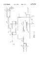
- a first gas streamis introduced into the plasma chamber 10 proximate to coils 12 through gas inlet line 22.
- the first gas streamincludes a mixture of oxygen and argon gases which are introduced to inlet line 22.
- the desired flow rates of the oxygen and argonare controlled by mass flow controllers 25 and 26, respectively.
- the inventionmay also be carried out with inert gases other than argon.
- the inert gasprovides a sputter etch component for simultaneous etching of the fluorinated silicon oxide layer during its deposition when the support 17 is biased.
- Other inert gases that may be usedare, any one of: argon, neon, xenon and krypton, or any mixture thereof.
- Heliummay also be used in combination with any one of argon, neon, xenon and krypton, or in combination with any mixture of argon, neon, xenon and krypton.
- the method of the inventionprovides for etching the substrate whereby an r.f. bias is applied to the support 17 through r.f. generator 19 and transmission line 18.
- the r.f. biasis applied creating a negative dc bias voltage on the support 17.
- the negative dc biaswill accelerate ions towards the surface of substrate 16.
Landscapes
- Chemical & Material Sciences (AREA)
- Engineering & Computer Science (AREA)
- Physics & Mathematics (AREA)
- Organic Chemistry (AREA)
- Metallurgy (AREA)
- Mechanical Engineering (AREA)
- Materials Engineering (AREA)
- Chemical Kinetics & Catalysis (AREA)
- Computer Hardware Design (AREA)
- Condensed Matter Physics & Semiconductors (AREA)
- General Physics & Mathematics (AREA)
- Power Engineering (AREA)
- Microelectronics & Electronic Packaging (AREA)
- Manufacturing & Machinery (AREA)
- General Chemical & Material Sciences (AREA)
- Inorganic Chemistry (AREA)
- Plasma & Fusion (AREA)
- Electromagnetism (AREA)
- Spectroscopy & Molecular Physics (AREA)
- Formation Of Insulating Films (AREA)
- Chemical Vapour Deposition (AREA)
- Internal Circuitry In Semiconductor Integrated Circuit Devices (AREA)
- Drying Of Semiconductors (AREA)
Abstract
Description
TABLE ______________________________________ Flow Rates: SiH.sub.4 40 sccm CF.sub.4 40 sccm O.sub.2 80 sccm Ar 40 sccm r.f. Frequency 13.56 MHz r.f. Bias Power 700 Watts Pressure 4-10 MTorr ______________________________________
Claims (19)
Priority Applications (7)
| Application Number | Priority Date | Filing Date | Title |
|---|---|---|---|
| US08/386,647US5571576A (en) | 1995-02-10 | 1995-02-10 | Method of forming a fluorinated silicon oxide layer using plasma chemical vapor deposition |
| JP08524377AJP3090476B2 (en) | 1995-02-10 | 1996-02-05 | Method of forming silicon fluoride oxide layer using plasma enhanced chemical vapor deposition |
| EP96906308AEP0757884B1 (en) | 1995-02-10 | 1996-02-05 | Method of forming a fluorinated silicon oxide layer using plasma chemical vapor deposition |
| KR1019960705764AKR100191850B1 (en) | 1995-02-10 | 1996-02-05 | Method of forming a fluorinated silicon oxide layer using plasma chemical vapor deposition |
| AT96906308TATE439028T1 (en) | 1995-02-10 | 1996-02-05 | METHOD FOR PRODUCING FLUORINATED SILICONE OXIDE LAYERS USING PLASMA CVD |
| PCT/US1996/001589WO1996025023A1 (en) | 1995-02-10 | 1996-02-05 | Method of forming a fluorinated silicon oxide layer using plasma chemical vapor deposition |
| DE69637982TDE69637982D1 (en) | 1995-02-10 | 1996-02-05 | METHOD FOR PRODUCING FLUORINATED SILICON OXIDE LAYERS USING PLASMA CVD |
Applications Claiming Priority (1)
| Application Number | Priority Date | Filing Date | Title |
|---|---|---|---|
| US08/386,647US5571576A (en) | 1995-02-10 | 1995-02-10 | Method of forming a fluorinated silicon oxide layer using plasma chemical vapor deposition |
Publications (1)
| Publication Number | Publication Date |
|---|---|
| US5571576Atrue US5571576A (en) | 1996-11-05 |
Family
ID=23526470
Family Applications (1)
| Application Number | Title | Priority Date | Filing Date |
|---|---|---|---|
| US08/386,647Expired - LifetimeUS5571576A (en) | 1995-02-10 | 1995-02-10 | Method of forming a fluorinated silicon oxide layer using plasma chemical vapor deposition |
Country Status (7)
| Country | Link |
|---|---|
| US (1) | US5571576A (en) |
| EP (1) | EP0757884B1 (en) |
| JP (1) | JP3090476B2 (en) |
| KR (1) | KR100191850B1 (en) |
| AT (1) | ATE439028T1 (en) |
| DE (1) | DE69637982D1 (en) |
| WO (1) | WO1996025023A1 (en) |
Cited By (224)
| Publication number | Priority date | Publication date | Assignee | Title |
|---|---|---|---|---|
| US5683946A (en)* | 1995-12-01 | 1997-11-04 | National Science Counsil | Method for manufacturing fluorinated gate oxide layer |
| US5733818A (en)* | 1995-10-18 | 1998-03-31 | Nec Corporation | Method for fabricating semiconductor device with planarization step using CMP |
| US5763021A (en)* | 1996-12-13 | 1998-06-09 | Cypress Semiconductor Corporation | Method of forming a dielectric film |
| US5827785A (en)* | 1996-10-24 | 1998-10-27 | Applied Materials, Inc. | Method for improving film stability of fluorosilicate glass films |
| US5869149A (en)* | 1997-06-30 | 1999-02-09 | Lam Research Corporation | Method for preparing nitrogen surface treated fluorine doped silicon dioxide films |
| US5876798A (en)* | 1997-12-29 | 1999-03-02 | Chartered Semiconductor Manufacturing, Ltd. | Method of fluorinated silicon oxide film deposition |
| US5894159A (en)* | 1994-06-09 | 1999-04-13 | Sony Corporation | Semiconductor device having first and second insulating layers |
| US5897711A (en)* | 1995-12-22 | 1999-04-27 | Lam Research Corporation | Method and apparatus for improving refractive index of dielectric films |
| US6042901A (en)* | 1996-02-20 | 2000-03-28 | Lam Research Corporation | Method for depositing fluorine doped silicon dioxide films |
| US6057250A (en)* | 1998-01-27 | 2000-05-02 | International Business Machines Corporation | Low temperature reflow dielectric-fluorinated BPSG |
| US6071573A (en)* | 1997-12-30 | 2000-06-06 | Lam Research Corporation | Process for precoating plasma CVD reactors |
| US6077574A (en)* | 1996-08-16 | 2000-06-20 | Nec Corporation | Plasma CVD process for forming a fluorine-doped SiO2 dielectric film |
| US6106678A (en)* | 1996-03-29 | 2000-08-22 | Lam Research Corporation | Method of high density plasma CVD gap-filling |
| US6106683A (en)* | 1997-06-23 | 2000-08-22 | Toyo Technologies Inc. | Grazing angle plasma polisher (GAPP) |
| US6121164A (en)* | 1997-10-24 | 2000-09-19 | Applied Materials, Inc. | Method for forming low compressive stress fluorinated ozone/TEOS oxide film |
| US6136685A (en)* | 1997-06-03 | 2000-10-24 | Applied Materials, Inc. | High deposition rate recipe for low dielectric constant films |
| US6140250A (en)* | 1996-05-27 | 2000-10-31 | Sony Corporation | Method for forming oxide film of semiconductor device, and oxide film forming apparatus capable of shortening pre-processing time for concentration measurement |
| US6149987A (en)* | 1998-04-07 | 2000-11-21 | Applied Materials, Inc. | Method for depositing low dielectric constant oxide films |
| DE19813757C2 (en)* | 1998-03-27 | 2000-12-14 | Siemens Ag | Process for the production of a fluorinated semiconductor surface |
| US6174743B1 (en)* | 1998-12-08 | 2001-01-16 | Advanced Micro Devices, Inc. | Method of reducing incidence of stress-induced voiding in semiconductor interconnect lines |
| US6221794B1 (en)* | 1998-12-08 | 2001-04-24 | Advanced Micro Devices, Inc. | Method of reducing incidence of stress-induced voiding in semiconductor interconnect lines |
| US6225228B1 (en) | 1996-12-04 | 2001-05-01 | Micron Technology, Inc. | Silicon oxide co-deposition/etching process |
| US6265779B1 (en)* | 1998-08-11 | 2001-07-24 | International Business Machines Corporation | Method and material for integration of fuorine-containing low-k dielectrics |
| US6291028B1 (en) | 1996-02-09 | 2001-09-18 | Applied Materials, Inc. | Method and apparatus for improving the film quality of plasma enhanced CVD films at the interface |
| US6326064B1 (en) | 1991-05-17 | 2001-12-04 | Lam Research Corporation | Process for depositing a SiOx film having reduced intrinsic stress and/or reduced hydrogen content |
| US6335288B1 (en) | 2000-08-24 | 2002-01-01 | Applied Materials, Inc. | Gas chemistry cycling to achieve high aspect ratio gapfill with HDP-CVD |
| US6355902B2 (en)* | 1996-11-14 | 2002-03-12 | Tokyo Electron Limited | Plasma film forming method and plasma film forming apparatus |
| US6394109B1 (en) | 1999-04-13 | 2002-05-28 | Applied Materials, Inc. | Method and apparatus for removing carbon contamination in a sub-atmospheric charged particle beam lithography system |
| US6395150B1 (en)* | 1998-04-01 | 2002-05-28 | Novellus Systems, Inc. | Very high aspect ratio gapfill using HDP |
| US20020078893A1 (en)* | 2000-05-18 | 2002-06-27 | Applied Materials , Inc. | Plasma enhanced chemical processing reactor and method |
| US20030003244A1 (en)* | 1998-03-20 | 2003-01-02 | Applied Materials, Inc. | Staggered in-situ deposition and etching of a dielectric layer for HDP CVD |
| US6503818B1 (en)* | 1999-04-02 | 2003-01-07 | Taiwan Semiconductor Manufacturing Company | Delamination resistant multi-layer composite dielectric layer employing low dielectric constant dielectric material |
| US6506662B2 (en) | 1995-09-25 | 2003-01-14 | Atsushi Ogura | Method for forming an SOI substrate by use of a plasma ion irradiation |
| US6541400B1 (en)* | 2000-02-09 | 2003-04-01 | Novellus Systems, Inc. | Process for CVD deposition of fluorinated silicon glass layer on semiconductor wafer |
| US6559052B2 (en) | 2000-07-07 | 2003-05-06 | Applied Materials, Inc. | Deposition of amorphous silicon films by high density plasma HDP-CVD at low temperatures |
| US20030136332A1 (en)* | 2002-01-24 | 2003-07-24 | Applied Materials Inc., A Delaware Corporation | In situ application of etch back for improved deposition into high-aspect-ratio features |
| US20030140941A1 (en)* | 1986-09-09 | 2003-07-31 | Semiconductor Energy Laboratory Co., Ltd. | CVD apparatus |
| US20030162034A1 (en)* | 2001-05-23 | 2003-08-28 | O'neill Mark Leonard | Low dielectric constant material and method of processing by CVD |
| US20030207580A1 (en)* | 2002-05-03 | 2003-11-06 | Applied Materials, Inc. | HDP-CVD dep/etch/dep process for improved deposition into high aspect ratio features |
| US6667248B2 (en) | 2001-09-05 | 2003-12-23 | Applied Materials Inc. | Low-bias-deposited high-density-plasma chemical-vapor-deposition silicate glass layers |
| US6716770B2 (en) | 2001-05-23 | 2004-04-06 | Air Products And Chemicals, Inc. | Low dielectric constant material and method of processing by CVD |
| US20040079632A1 (en)* | 2002-10-23 | 2004-04-29 | Applied Materials, Inc. | High density plasma CVD process for gapfill into high aspect ratio features |
| US20040079728A1 (en)* | 2002-10-23 | 2004-04-29 | Applied Materials, Inc. | Reactive ion etching for semiconductor device feature topography modification |
| US6740601B2 (en) | 2001-05-11 | 2004-05-25 | Applied Materials Inc. | HDP-CVD deposition process for filling high aspect ratio gaps |
| US6746726B2 (en)* | 1998-03-27 | 2004-06-08 | Tokyo University Of Agriculture & Technology | Method for forming film |
| US6753270B1 (en) | 2000-08-04 | 2004-06-22 | Applied Materials Inc. | Process for depositing a porous, low dielectric constant silicon oxide film |
| US20040149388A1 (en)* | 2000-10-19 | 2004-08-05 | Klaus Breitschwerdt | Device and method for etching a substrate by using an inductively coupled plasma |
| WO2004013371A3 (en)* | 2002-08-02 | 2004-10-21 | Varian Semiconductor Equipment | Method and apparatus for plasma implantation without deposition of a layer of byproduct |
| US20040245091A1 (en)* | 2003-06-04 | 2004-12-09 | Applied Materials, Inc. | Hdp-cvd multistep gapfill process |
| US20040251236A1 (en)* | 2003-05-23 | 2004-12-16 | Applied Materials, Inc. | [deposition-selective etch-deposition process for dielectric film gapfill] |
| US6846391B1 (en) | 1998-04-01 | 2005-01-25 | Novellus Systems | Process for depositing F-doped silica glass in high aspect ratio structures |
| US20050019494A1 (en)* | 2003-07-25 | 2005-01-27 | Applied Materials, Inc., A Delaware Corporation | Sequential gas flow oxide deposition technique |
| US20050087833A1 (en)* | 1995-10-24 | 2005-04-28 | Schuegraf Klaus F. | Shallow trench isolation using low dielectric constant insulator |
| US20050098856A1 (en)* | 2001-02-23 | 2005-05-12 | Sheldon Aronowitz | Low dielectric constant fluorine and carbon-containing silicon oxide dielectric material characterized by improved resistance to oxidation |
| US6903031B2 (en) | 2003-09-03 | 2005-06-07 | Applied Materials, Inc. | In-situ-etch-assisted HDP deposition using SiF4 and hydrogen |
| US6929700B2 (en) | 2001-05-11 | 2005-08-16 | Applied Materials, Inc. | Hydrogen assisted undoped silicon oxide deposition process for HDP-CVD |
| US6958112B2 (en) | 2003-05-27 | 2005-10-25 | Applied Materials, Inc. | Methods and systems for high-aspect-ratio gapfill using atomic-oxygen generation |
| US20060000797A1 (en)* | 2004-06-30 | 2006-01-05 | Adams Yoko Y | Methods and apparatus for the optimization of etch resistance in a plasma processing system |
| US20060154494A1 (en)* | 2005-01-08 | 2006-07-13 | Applied Materials, Inc., A Delaware Corporation | High-throughput HDP-CVD processes for advanced gapfill applications |
| US7087536B2 (en) | 2004-09-01 | 2006-08-08 | Applied Materials | Silicon oxide gapfill deposition using liquid precursors |
| US20060292894A1 (en)* | 2005-06-24 | 2006-12-28 | Applied Materials, Inc., | Gapfill using deposition-etch sequence |
| US7183227B1 (en) | 2004-07-01 | 2007-02-27 | Applied Materials, Inc. | Use of enhanced turbomolecular pump for gapfill deposition using high flows of low-mass fluent gas |
| US20070111543A1 (en)* | 2005-11-15 | 2007-05-17 | Applied Materials, Inc. | Methods for improving low k FSG film gap-fill characteristics |
| US7229931B2 (en) | 2004-06-16 | 2007-06-12 | Applied Materials, Inc. | Oxygen plasma treatment for enhanced HDP-CVD gapfill |
| US20080205838A1 (en)* | 2004-07-22 | 2008-08-28 | Davide Diego Crippa | Optical Device Including a Buried Grating With Air Filled Voids and Method For Realising It |
| US7524750B2 (en) | 2006-04-17 | 2009-04-28 | Applied Materials, Inc. | Integrated process modulation (IPM) a novel solution for gapfill with HDP-CVD |
| US7595088B2 (en) | 2003-01-23 | 2009-09-29 | Applied Materials, Inc. | Hydrogen assisted HDP-CVD deposition process for aggressive gap-fill technology |
| US7678715B2 (en) | 2007-12-21 | 2010-03-16 | Applied Materials, Inc. | Low wet etch rate silicon nitride film |
| US7939422B2 (en) | 2006-12-07 | 2011-05-10 | Applied Materials, Inc. | Methods of thin film process |
| US20120000772A1 (en)* | 2010-07-02 | 2012-01-05 | Applied Materials, Inc. | Deposition Apparatus And Methods To Reduce Deposition Asymmetry |
| WO2013109427A1 (en)* | 2012-01-18 | 2013-07-25 | Applied Materials, Inc. | Multi-zone direct gas flow control of a substrate processing chamber |
| US8497211B2 (en) | 2011-06-24 | 2013-07-30 | Applied Materials, Inc. | Integrated process modulation for PSG gapfill |
| US8679982B2 (en) | 2011-08-26 | 2014-03-25 | Applied Materials, Inc. | Selective suppression of dry-etch rate of materials containing both silicon and oxygen |
| US8679983B2 (en) | 2011-09-01 | 2014-03-25 | Applied Materials, Inc. | Selective suppression of dry-etch rate of materials containing both silicon and nitrogen |
| US8741778B2 (en) | 2010-12-14 | 2014-06-03 | Applied Materials, Inc. | Uniform dry etch in two stages |
| US8765574B2 (en) | 2012-11-09 | 2014-07-01 | Applied Materials, Inc. | Dry etch process |
| US8771539B2 (en) | 2011-02-22 | 2014-07-08 | Applied Materials, Inc. | Remotely-excited fluorine and water vapor etch |
| US8771536B2 (en) | 2011-08-01 | 2014-07-08 | Applied Materials, Inc. | Dry-etch for silicon-and-carbon-containing films |
| US8801952B1 (en) | 2013-03-07 | 2014-08-12 | Applied Materials, Inc. | Conformal oxide dry etch |
| US8808563B2 (en) | 2011-10-07 | 2014-08-19 | Applied Materials, Inc. | Selective etch of silicon by way of metastable hydrogen termination |
| US8895449B1 (en) | 2013-05-16 | 2014-11-25 | Applied Materials, Inc. | Delicate dry clean |
| US8921234B2 (en) | 2012-12-21 | 2014-12-30 | Applied Materials, Inc. | Selective titanium nitride etching |
| US8927390B2 (en) | 2011-09-26 | 2015-01-06 | Applied Materials, Inc. | Intrench profile |
| US8951429B1 (en) | 2013-10-29 | 2015-02-10 | Applied Materials, Inc. | Tungsten oxide processing |
| US8956980B1 (en) | 2013-09-16 | 2015-02-17 | Applied Materials, Inc. | Selective etch of silicon nitride |
| US8969212B2 (en) | 2012-11-20 | 2015-03-03 | Applied Materials, Inc. | Dry-etch selectivity |
| US8975152B2 (en) | 2011-11-08 | 2015-03-10 | Applied Materials, Inc. | Methods of reducing substrate dislocation during gapfill processing |
| US8980763B2 (en) | 2012-11-30 | 2015-03-17 | Applied Materials, Inc. | Dry-etch for selective tungsten removal |
| US8999856B2 (en) | 2011-03-14 | 2015-04-07 | Applied Materials, Inc. | Methods for etch of sin films |
| US9018108B2 (en) | 2013-01-25 | 2015-04-28 | Applied Materials, Inc. | Low shrinkage dielectric films |
| US9023734B2 (en) | 2012-09-18 | 2015-05-05 | Applied Materials, Inc. | Radical-component oxide etch |
| US9023732B2 (en) | 2013-03-15 | 2015-05-05 | Applied Materials, Inc. | Processing systems and methods for halide scavenging |
| US9034770B2 (en) | 2012-09-17 | 2015-05-19 | Applied Materials, Inc. | Differential silicon oxide etch |
| US9040422B2 (en) | 2013-03-05 | 2015-05-26 | Applied Materials, Inc. | Selective titanium nitride removal |
| US9064816B2 (en) | 2012-11-30 | 2015-06-23 | Applied Materials, Inc. | Dry-etch for selective oxidation removal |
| US9064815B2 (en) | 2011-03-14 | 2015-06-23 | Applied Materials, Inc. | Methods for etch of metal and metal-oxide films |
| US9111877B2 (en) | 2012-12-18 | 2015-08-18 | Applied Materials, Inc. | Non-local plasma oxide etch |
| US9117855B2 (en) | 2013-12-04 | 2015-08-25 | Applied Materials, Inc. | Polarity control for remote plasma |
| US9114438B2 (en) | 2013-05-21 | 2015-08-25 | Applied Materials, Inc. | Copper residue chamber clean |
| US9132436B2 (en) | 2012-09-21 | 2015-09-15 | Applied Materials, Inc. | Chemical control features in wafer process equipment |
| US9136273B1 (en) | 2014-03-21 | 2015-09-15 | Applied Materials, Inc. | Flash gate air gap |
| US9159606B1 (en) | 2014-07-31 | 2015-10-13 | Applied Materials, Inc. | Metal air gap |
| US9165786B1 (en) | 2014-08-05 | 2015-10-20 | Applied Materials, Inc. | Integrated oxide and nitride recess for better channel contact in 3D architectures |
| US9190293B2 (en) | 2013-12-18 | 2015-11-17 | Applied Materials, Inc. | Even tungsten etch for high aspect ratio trenches |
| US9236265B2 (en) | 2013-11-04 | 2016-01-12 | Applied Materials, Inc. | Silicon germanium processing |
| US9245762B2 (en) | 2013-12-02 | 2016-01-26 | Applied Materials, Inc. | Procedure for etch rate consistency |
| US9263278B2 (en) | 2013-12-17 | 2016-02-16 | Applied Materials, Inc. | Dopant etch selectivity control |
| US9269590B2 (en) | 2014-04-07 | 2016-02-23 | Applied Materials, Inc. | Spacer formation |
| US9287134B2 (en) | 2014-01-17 | 2016-03-15 | Applied Materials, Inc. | Titanium oxide etch |
| US9287095B2 (en) | 2013-12-17 | 2016-03-15 | Applied Materials, Inc. | Semiconductor system assemblies and methods of operation |
| US9293568B2 (en) | 2014-01-27 | 2016-03-22 | Applied Materials, Inc. | Method of fin patterning |
| US9299537B2 (en) | 2014-03-20 | 2016-03-29 | Applied Materials, Inc. | Radial waveguide systems and methods for post-match control of microwaves |
| US9299538B2 (en) | 2014-03-20 | 2016-03-29 | Applied Materials, Inc. | Radial waveguide systems and methods for post-match control of microwaves |
| US9299582B2 (en) | 2013-11-12 | 2016-03-29 | Applied Materials, Inc. | Selective etch for metal-containing materials |
| US9299583B1 (en) | 2014-12-05 | 2016-03-29 | Applied Materials, Inc. | Aluminum oxide selective etch |
| US9299575B2 (en) | 2014-03-17 | 2016-03-29 | Applied Materials, Inc. | Gas-phase tungsten etch |
| US9309598B2 (en) | 2014-05-28 | 2016-04-12 | Applied Materials, Inc. | Oxide and metal removal |
| US9324576B2 (en) | 2010-05-27 | 2016-04-26 | Applied Materials, Inc. | Selective etch for silicon films |
| US9343272B1 (en) | 2015-01-08 | 2016-05-17 | Applied Materials, Inc. | Self-aligned process |
| US9349605B1 (en) | 2015-08-07 | 2016-05-24 | Applied Materials, Inc. | Oxide etch selectivity systems and methods |
| US9355862B2 (en) | 2014-09-24 | 2016-05-31 | Applied Materials, Inc. | Fluorine-based hardmask removal |
| US9355856B2 (en) | 2014-09-12 | 2016-05-31 | Applied Materials, Inc. | V trench dry etch |
| US9362130B2 (en) | 2013-03-01 | 2016-06-07 | Applied Materials, Inc. | Enhanced etching processes using remote plasma sources |
| US9368364B2 (en) | 2014-09-24 | 2016-06-14 | Applied Materials, Inc. | Silicon etch process with tunable selectivity to SiO2 and other materials |
| US9373517B2 (en) | 2012-08-02 | 2016-06-21 | Applied Materials, Inc. | Semiconductor processing with DC assisted RF power for improved control |
| US9373522B1 (en) | 2015-01-22 | 2016-06-21 | Applied Mateials, Inc. | Titanium nitride removal |
| US9378978B2 (en) | 2014-07-31 | 2016-06-28 | Applied Materials, Inc. | Integrated oxide recess and floating gate fin trimming |
| US9378969B2 (en) | 2014-06-19 | 2016-06-28 | Applied Materials, Inc. | Low temperature gas-phase carbon removal |
| US9385028B2 (en) | 2014-02-03 | 2016-07-05 | Applied Materials, Inc. | Air gap process |
| US9390937B2 (en) | 2012-09-20 | 2016-07-12 | Applied Materials, Inc. | Silicon-carbon-nitride selective etch |
| US9396989B2 (en) | 2014-01-27 | 2016-07-19 | Applied Materials, Inc. | Air gaps between copper lines |
| US9406523B2 (en) | 2014-06-19 | 2016-08-02 | Applied Materials, Inc. | Highly selective doped oxide removal method |
| US9425058B2 (en) | 2014-07-24 | 2016-08-23 | Applied Materials, Inc. | Simplified litho-etch-litho-etch process |
| US9449846B2 (en) | 2015-01-28 | 2016-09-20 | Applied Materials, Inc. | Vertical gate separation |
| US9478432B2 (en) | 2014-09-25 | 2016-10-25 | Applied Materials, Inc. | Silicon oxide selective removal |
| US9493879B2 (en) | 2013-07-12 | 2016-11-15 | Applied Materials, Inc. | Selective sputtering for pattern transfer |
| US9496167B2 (en) | 2014-07-31 | 2016-11-15 | Applied Materials, Inc. | Integrated bit-line airgap formation and gate stack post clean |
| US9502258B2 (en) | 2014-12-23 | 2016-11-22 | Applied Materials, Inc. | Anisotropic gap etch |
| US9499898B2 (en) | 2014-03-03 | 2016-11-22 | Applied Materials, Inc. | Layered thin film heater and method of fabrication |
| US9553102B2 (en) | 2014-08-19 | 2017-01-24 | Applied Materials, Inc. | Tungsten separation |
| US9576809B2 (en) | 2013-11-04 | 2017-02-21 | Applied Materials, Inc. | Etch suppression with germanium |
| US9659753B2 (en) | 2014-08-07 | 2017-05-23 | Applied Materials, Inc. | Grooved insulator to reduce leakage current |
| US9691645B2 (en) | 2015-08-06 | 2017-06-27 | Applied Materials, Inc. | Bolted wafer chuck thermal management systems and methods for wafer processing systems |
| US9721789B1 (en) | 2016-10-04 | 2017-08-01 | Applied Materials, Inc. | Saving ion-damaged spacers |
| US9728437B2 (en) | 2015-02-03 | 2017-08-08 | Applied Materials, Inc. | High temperature chuck for plasma processing systems |
| US9741593B2 (en) | 2015-08-06 | 2017-08-22 | Applied Materials, Inc. | Thermal management systems and methods for wafer processing systems |
| US9768034B1 (en) | 2016-11-11 | 2017-09-19 | Applied Materials, Inc. | Removal methods for high aspect ratio structures |
| US9773648B2 (en) | 2013-08-30 | 2017-09-26 | Applied Materials, Inc. | Dual discharge modes operation for remote plasma |
| US9847289B2 (en) | 2014-05-30 | 2017-12-19 | Applied Materials, Inc. | Protective via cap for improved interconnect performance |
| US9865484B1 (en) | 2016-06-29 | 2018-01-09 | Applied Materials, Inc. | Selective etch using material modification and RF pulsing |
| US9881805B2 (en) | 2015-03-02 | 2018-01-30 | Applied Materials, Inc. | Silicon selective removal |
| US9885117B2 (en) | 2014-03-31 | 2018-02-06 | Applied Materials, Inc. | Conditioned semiconductor system parts |
| US9934942B1 (en) | 2016-10-04 | 2018-04-03 | Applied Materials, Inc. | Chamber with flow-through source |
| US9947549B1 (en) | 2016-10-10 | 2018-04-17 | Applied Materials, Inc. | Cobalt-containing material removal |
| US10026621B2 (en) | 2016-11-14 | 2018-07-17 | Applied Materials, Inc. | SiN spacer profile patterning |
| US10043684B1 (en) | 2017-02-06 | 2018-08-07 | Applied Materials, Inc. | Self-limiting atomic thermal etching systems and methods |
| US10043674B1 (en) | 2017-08-04 | 2018-08-07 | Applied Materials, Inc. | Germanium etching systems and methods |
| US10049891B1 (en) | 2017-05-31 | 2018-08-14 | Applied Materials, Inc. | Selective in situ cobalt residue removal |
| US10062585B2 (en) | 2016-10-04 | 2018-08-28 | Applied Materials, Inc. | Oxygen compatible plasma source |
| US10062587B2 (en) | 2012-07-18 | 2018-08-28 | Applied Materials, Inc. | Pedestal with multi-zone temperature control and multiple purge capabilities |
| US10062575B2 (en) | 2016-09-09 | 2018-08-28 | Applied Materials, Inc. | Poly directional etch by oxidation |
| US10062579B2 (en) | 2016-10-07 | 2018-08-28 | Applied Materials, Inc. | Selective SiN lateral recess |
| US10128086B1 (en) | 2017-10-24 | 2018-11-13 | Applied Materials, Inc. | Silicon pretreatment for nitride removal |
| US10163696B2 (en) | 2016-11-11 | 2018-12-25 | Applied Materials, Inc. | Selective cobalt removal for bottom up gapfill |
| US10170282B2 (en) | 2013-03-08 | 2019-01-01 | Applied Materials, Inc. | Insulated semiconductor faceplate designs |
| US10170336B1 (en) | 2017-08-04 | 2019-01-01 | Applied Materials, Inc. | Methods for anisotropic control of selective silicon removal |
| US10224210B2 (en) | 2014-12-09 | 2019-03-05 | Applied Materials, Inc. | Plasma processing system with direct outlet toroidal plasma source |
| US10242908B2 (en) | 2016-11-14 | 2019-03-26 | Applied Materials, Inc. | Airgap formation with damage-free copper |
| US10256112B1 (en) | 2017-12-08 | 2019-04-09 | Applied Materials, Inc. | Selective tungsten removal |
| US10256079B2 (en) | 2013-02-08 | 2019-04-09 | Applied Materials, Inc. | Semiconductor processing systems having multiple plasma configurations |
| US10283324B1 (en) | 2017-10-24 | 2019-05-07 | Applied Materials, Inc. | Oxygen treatment for nitride etching |
| US10283321B2 (en) | 2011-01-18 | 2019-05-07 | Applied Materials, Inc. | Semiconductor processing system and methods using capacitively coupled plasma |
| US10297458B2 (en) | 2017-08-07 | 2019-05-21 | Applied Materials, Inc. | Process window widening using coated parts in plasma etch processes |
| US10319739B2 (en) | 2017-02-08 | 2019-06-11 | Applied Materials, Inc. | Accommodating imperfectly aligned memory holes |
| US10319649B2 (en) | 2017-04-11 | 2019-06-11 | Applied Materials, Inc. | Optical emission spectroscopy (OES) for remote plasma monitoring |
| US10319600B1 (en) | 2018-03-12 | 2019-06-11 | Applied Materials, Inc. | Thermal silicon etch |
| US10354889B2 (en) | 2017-07-17 | 2019-07-16 | Applied Materials, Inc. | Non-halogen etching of silicon-containing materials |
| US10403507B2 (en) | 2017-02-03 | 2019-09-03 | Applied Materials, Inc. | Shaped etch profile with oxidation |
| US10431429B2 (en) | 2017-02-03 | 2019-10-01 | Applied Materials, Inc. | Systems and methods for radial and azimuthal control of plasma uniformity |
| US10468267B2 (en) | 2017-05-31 | 2019-11-05 | Applied Materials, Inc. | Water-free etching methods |
| US10490406B2 (en) | 2018-04-10 | 2019-11-26 | Appled Materials, Inc. | Systems and methods for material breakthrough |
| US10490418B2 (en) | 2014-10-14 | 2019-11-26 | Applied Materials, Inc. | Systems and methods for internal surface conditioning assessment in plasma processing equipment |
| US10497573B2 (en) | 2018-03-13 | 2019-12-03 | Applied Materials, Inc. | Selective atomic layer etching of semiconductor materials |
| US10504754B2 (en) | 2016-05-19 | 2019-12-10 | Applied Materials, Inc. | Systems and methods for improved semiconductor etching and component protection |
| US10504700B2 (en) | 2015-08-27 | 2019-12-10 | Applied Materials, Inc. | Plasma etching systems and methods with secondary plasma injection |
| US10522371B2 (en) | 2016-05-19 | 2019-12-31 | Applied Materials, Inc. | Systems and methods for improved semiconductor etching and component protection |
| US10541184B2 (en) | 2017-07-11 | 2020-01-21 | Applied Materials, Inc. | Optical emission spectroscopic techniques for monitoring etching |
| US10541246B2 (en) | 2017-06-26 | 2020-01-21 | Applied Materials, Inc. | 3D flash memory cells which discourage cross-cell electrical tunneling |
| US10546729B2 (en) | 2016-10-04 | 2020-01-28 | Applied Materials, Inc. | Dual-channel showerhead with improved profile |
| US10566206B2 (en) | 2016-12-27 | 2020-02-18 | Applied Materials, Inc. | Systems and methods for anisotropic material breakthrough |
| US10573496B2 (en) | 2014-12-09 | 2020-02-25 | Applied Materials, Inc. | Direct outlet toroidal plasma source |
| US10573527B2 (en) | 2018-04-06 | 2020-02-25 | Applied Materials, Inc. | Gas-phase selective etching systems and methods |
| US10593560B2 (en) | 2018-03-01 | 2020-03-17 | Applied Materials, Inc. | Magnetic induction plasma source for semiconductor processes and equipment |
| US10593523B2 (en) | 2014-10-14 | 2020-03-17 | Applied Materials, Inc. | Systems and methods for internal surface conditioning in plasma processing equipment |
| US10615047B2 (en) | 2018-02-28 | 2020-04-07 | Applied Materials, Inc. | Systems and methods to form airgaps |
| US10629473B2 (en) | 2016-09-09 | 2020-04-21 | Applied Materials, Inc. | Footing removal for nitride spacer |
| US10672642B2 (en) | 2018-07-24 | 2020-06-02 | Applied Materials, Inc. | Systems and methods for pedestal configuration |
| US10679870B2 (en) | 2018-02-15 | 2020-06-09 | Applied Materials, Inc. | Semiconductor processing chamber multistage mixing apparatus |
| US10699879B2 (en) | 2018-04-17 | 2020-06-30 | Applied Materials, Inc. | Two piece electrode assembly with gap for plasma control |
| US10727080B2 (en) | 2017-07-07 | 2020-07-28 | Applied Materials, Inc. | Tantalum-containing material removal |
| US10755941B2 (en) | 2018-07-06 | 2020-08-25 | Applied Materials, Inc. | Self-limiting selective etching systems and methods |
| US10854426B2 (en) | 2018-01-08 | 2020-12-01 | Applied Materials, Inc. | Metal recess for semiconductor structures |
| US10872778B2 (en) | 2018-07-06 | 2020-12-22 | Applied Materials, Inc. | Systems and methods utilizing solid-phase etchants |
| US10886137B2 (en) | 2018-04-30 | 2021-01-05 | Applied Materials, Inc. | Selective nitride removal |
| US10892198B2 (en) | 2018-09-14 | 2021-01-12 | Applied Materials, Inc. | Systems and methods for improved performance in semiconductor processing |
| US10903054B2 (en) | 2017-12-19 | 2021-01-26 | Applied Materials, Inc. | Multi-zone gas distribution systems and methods |
| US10920320B2 (en) | 2017-06-16 | 2021-02-16 | Applied Materials, Inc. | Plasma health determination in semiconductor substrate processing reactors |
| US10920319B2 (en) | 2019-01-11 | 2021-02-16 | Applied Materials, Inc. | Ceramic showerheads with conductive electrodes |
| US10943834B2 (en) | 2017-03-13 | 2021-03-09 | Applied Materials, Inc. | Replacement contact process |
| US10964512B2 (en) | 2018-02-15 | 2021-03-30 | Applied Materials, Inc. | Semiconductor processing chamber multistage mixing apparatus and methods |
| US11049755B2 (en) | 2018-09-14 | 2021-06-29 | Applied Materials, Inc. | Semiconductor substrate supports with embedded RF shield |
| US11062887B2 (en) | 2018-09-17 | 2021-07-13 | Applied Materials, Inc. | High temperature RF heater pedestals |
| US11121002B2 (en) | 2018-10-24 | 2021-09-14 | Applied Materials, Inc. | Systems and methods for etching metals and metal derivatives |
| US11239061B2 (en) | 2014-11-26 | 2022-02-01 | Applied Materials, Inc. | Methods and systems to enhance process uniformity |
| US11257693B2 (en) | 2015-01-09 | 2022-02-22 | Applied Materials, Inc. | Methods and systems to improve pedestal temperature control |
| US11276590B2 (en) | 2017-05-17 | 2022-03-15 | Applied Materials, Inc. | Multi-zone semiconductor substrate supports |
| US11276559B2 (en) | 2017-05-17 | 2022-03-15 | Applied Materials, Inc. | Semiconductor processing chamber for multiple precursor flow |
| US11328909B2 (en) | 2017-12-22 | 2022-05-10 | Applied Materials, Inc. | Chamber conditioning and removal processes |
| US11417534B2 (en) | 2018-09-21 | 2022-08-16 | Applied Materials, Inc. | Selective material removal |
| US11437242B2 (en) | 2018-11-27 | 2022-09-06 | Applied Materials, Inc. | Selective removal of silicon-containing materials |
| US11594428B2 (en) | 2015-02-03 | 2023-02-28 | Applied Materials, Inc. | Low temperature chuck for plasma processing systems |
| US11682560B2 (en) | 2018-10-11 | 2023-06-20 | Applied Materials, Inc. | Systems and methods for hafnium-containing film removal |
| US11721527B2 (en) | 2019-01-07 | 2023-08-08 | Applied Materials, Inc. | Processing chamber mixing systems |
| US12340979B2 (en) | 2017-05-17 | 2025-06-24 | Applied Materials, Inc. | Semiconductor processing chamber for improved precursor flow |
Families Citing this family (8)
| Publication number | Priority date | Publication date | Assignee | Title |
|---|---|---|---|---|
| TW335511B (en)* | 1996-08-02 | 1998-07-01 | Applied Materials Inc | Stress control by fluorination of silica film |
| JP3773340B2 (en)* | 1996-12-18 | 2006-05-10 | 大日本印刷株式会社 | Low refractive index SiO2 film and manufacturing method thereof |
| US6184158B1 (en)* | 1996-12-23 | 2001-02-06 | Lam Research Corporation | Inductively coupled plasma CVD |
| JPH10242142A (en)* | 1997-02-21 | 1998-09-11 | Nippon Asm Kk | Semiconductor device and manufacturing method thereof |
| JP4056144B2 (en)* | 1998-09-10 | 2008-03-05 | 株式会社エフオーアイ | Plasma processing equipment |
| JP4105353B2 (en)* | 1999-07-26 | 2008-06-25 | 財団法人国際科学振興財団 | Semiconductor device |
| US6383954B1 (en)* | 1999-07-27 | 2002-05-07 | Applied Materials, Inc. | Process gas distribution for forming stable fluorine-doped silicate glass and other films |
| KR102521768B1 (en)* | 2021-02-16 | 2023-04-19 | 인투코어테크놀로지 주식회사 | A method of processing gas using plasma |
Citations (10)
| Publication number | Priority date | Publication date | Assignee | Title |
|---|---|---|---|---|
| US4668365A (en)* | 1984-10-25 | 1987-05-26 | Applied Materials, Inc. | Apparatus and method for magnetron-enhanced plasma-assisted chemical vapor deposition |
| US4960071A (en)* | 1987-09-30 | 1990-10-02 | Sumitomo Metal Industries Ltd. | Thin film forming apparatus |
| US4987102A (en)* | 1989-12-04 | 1991-01-22 | Motorola, Inc. | Process for forming high purity thin films |
| US5057455A (en)* | 1989-11-30 | 1991-10-15 | At&T Bell Laboratories | Formation of integrated circuit electrodes |
| US5124014A (en)* | 1990-02-27 | 1992-06-23 | At&T Bell Laboratories | Method of forming oxide layers by bias ECR plasma deposition |
| US5215787A (en)* | 1991-01-23 | 1993-06-01 | Nec Corporation | Method of forming silicon oxide film containing fluorine |
| US5240554A (en)* | 1991-01-22 | 1993-08-31 | Kabushiki Kaisha Toshiba | Method of manufacturing semiconductor device |
| US5288518A (en)* | 1991-06-07 | 1994-02-22 | Nec Corproation | Chemical vapor deposition method for forming fluorine containing silicon oxide film |
| US5296404A (en)* | 1990-10-24 | 1994-03-22 | Sumitomo Metal Industries, Ltd. | Method for forming a thin film for a semiconductor device |
| US5334552A (en)* | 1991-12-04 | 1994-08-02 | Nec Corporation | Method for fabricating a semiconductor device having a multi-layered interconnection structure |
Family Cites Families (3)
| Publication number | Priority date | Publication date | Assignee | Title |
|---|---|---|---|---|
| US5000113A (en)* | 1986-12-19 | 1991-03-19 | Applied Materials, Inc. | Thermal CVD/PECVD reactor and use for thermal chemical vapor deposition of silicon dioxide and in-situ multi-step planarized process |
| US4894352A (en)* | 1988-10-26 | 1990-01-16 | Texas Instruments Inc. | Deposition of silicon-containing films using organosilicon compounds and nitrogen trifluoride |
| JPH0793275B2 (en)* | 1993-06-25 | 1995-10-09 | アプライド マテリアルズ インコーポレイテッド | Thin film of semiconductor device and thin film forming method of semiconductor device |
- 1995
- 1995-02-10USUS08/386,647patent/US5571576A/ennot_activeExpired - Lifetime
- 1996
- 1996-02-05KRKR1019960705764Apatent/KR100191850B1/ennot_activeExpired - Fee Related
- 1996-02-05JPJP08524377Apatent/JP3090476B2/ennot_activeExpired - Fee Related
- 1996-02-05EPEP96906308Apatent/EP0757884B1/ennot_activeExpired - Lifetime
- 1996-02-05WOPCT/US1996/001589patent/WO1996025023A1/enactiveApplication Filing
- 1996-02-05DEDE69637982Tpatent/DE69637982D1/ennot_activeExpired - Lifetime
- 1996-02-05ATAT96906308Tpatent/ATE439028T1/ennot_activeIP Right Cessation
Patent Citations (10)
| Publication number | Priority date | Publication date | Assignee | Title |
|---|---|---|---|---|
| US4668365A (en)* | 1984-10-25 | 1987-05-26 | Applied Materials, Inc. | Apparatus and method for magnetron-enhanced plasma-assisted chemical vapor deposition |
| US4960071A (en)* | 1987-09-30 | 1990-10-02 | Sumitomo Metal Industries Ltd. | Thin film forming apparatus |
| US5057455A (en)* | 1989-11-30 | 1991-10-15 | At&T Bell Laboratories | Formation of integrated circuit electrodes |
| US4987102A (en)* | 1989-12-04 | 1991-01-22 | Motorola, Inc. | Process for forming high purity thin films |
| US5124014A (en)* | 1990-02-27 | 1992-06-23 | At&T Bell Laboratories | Method of forming oxide layers by bias ECR plasma deposition |
| US5296404A (en)* | 1990-10-24 | 1994-03-22 | Sumitomo Metal Industries, Ltd. | Method for forming a thin film for a semiconductor device |
| US5240554A (en)* | 1991-01-22 | 1993-08-31 | Kabushiki Kaisha Toshiba | Method of manufacturing semiconductor device |
| US5215787A (en)* | 1991-01-23 | 1993-06-01 | Nec Corporation | Method of forming silicon oxide film containing fluorine |
| US5288518A (en)* | 1991-06-07 | 1994-02-22 | Nec Corproation | Chemical vapor deposition method for forming fluorine containing silicon oxide film |
| US5334552A (en)* | 1991-12-04 | 1994-08-02 | Nec Corporation | Method for fabricating a semiconductor device having a multi-layered interconnection structure |
Non-Patent Citations (50)
| Title |
|---|
| 17th Internation Conference on Metallurgical Coatings and 8th International Conference on Thin Films, San Diego, CA, USA, Apr. 2 6, 1990, pp. 269 278 Low Temperature SiO 2 Films Falcony, Ortiz, Lopez, Alonso & Muhl (no month avail.).* |
| 17th Internation Conference on Metallurgical Coatings and 8th International Conference on Thin Films, San Diego, CA, USA, Apr. 2-6, 1990, pp. 269-278--Low Temperature SiO2 Films--Falcony, Ortiz, Lopez, Alonso & Muhl (no month avail.). |
| 1988 American Institute of Physics, J. Appl. Phys. 64 (7), 1 Oct. 1988, pp. 3481 3486 Bonding Configuration of Fluorine in Fluorinated Silicon Nitride Films Fujita, Toyoshima, & Sasaki (no month avail.).* |
| 1988 American Institute of Physics, J. Appl. Phys. 64 (7), 1 Oct. 1988, pp. 3481-3486--Bonding Configuration of Fluorine in Fluorinated Silicon Nitride Films--Fujita, Toyoshima, & Sasaki (no month avail.). |
| 1993 Dry Process Symposium, Tokyo High Quality and Low Dielectric Constant SiO 2 CVD Using High Density Plasma Hayasaka, Nishiyama, Miyajima, Tomioka, Nakata & Okano (no month avail).* |
| 1993 Dry Process Symposium, Tokyo, pp. 163 168 High Quality and Low Dielectric Constant SiO 2 CVD Using High Density Plasma Hayasaka, Nishiyama, Miyajima, Tomioka, Nakata & Okano (no month avail.).* |
| 1993 Dry Process Symposium, Tokyo, pp. 163-168--High-Quality and Low Dielectric Constant SiO2 CVD Using High Density Plasma--Hayasaka, Nishiyama, Miyajima, Tomioka, Nakata & Okano (no month avail.). |
| 1993 Dry Process Symposium, Tokyo--High-Quality and Low Dielectric Constant SiO2 CVD Using High Density Plasma--Hayasaka, Nishiyama, Miyajima, Tomioka, Nakata & Okano (no month avail). |
| 1993 International conference on Solid State Device and Materials, Makuhari, 1993, pp. 158 160 Preparation of SiOF Films With Low Dielectric Constant by ECR Plasma Chemical Vapor Deposition Fukada and Akahori (no month avail.).* |
| 1993 International conference on Solid State Device and Materials, Makuhari, 1993, pp. 158-160--Preparation of SiOF Films With Low Dielectric Constant by ECR Plasma Chemical Vapor Deposition--Fukada and Akahori (no month avail.). |
| 1994 Symposium on VLSI Technology Digest of Technical Papers, pp. 59 60 Reduction of Wiring Capacitance with New Low Dielectric SiOF Interlayer Film for High Speed/Low Power Sub Half Micron CMOS Ida, Yoshimaru, Usami, Ohtomo, Shimokawa, Kita & Ino (no month avail.).* |
| 1994 Symposium on VLSI Technology Digest of Technical Papers, pp. 59-60--Reduction of Wiring Capacitance with New Low Dielectric SiOF Interlayer Film for High Speed/Low Power Sub-Half Micron CMOS--Ida, Yoshimaru, Usami, Ohtomo, Shimokawa, Kita & Ino (no month avail.). |
| 1994 Symposium on VLSI Technology Digest of Technical Papers, pp. 73 74 A Planarized Multilevel Interconnect Scheme with Embedded Low Dielectric Constant Polymers for Sub Quarter Micron Applications Jeng, Chang, Kroger, McAnally, Havemann (no month avail.).* |
| 1994 Symposium on VLSI Technology Digest of Technical Papers, pp. 73-74--A Planarized Multilevel Interconnect Scheme with Embedded Low-Dielectric-Constant Polymers for Sub-Quarter-Micron Applications--Jeng, Chang, Kroger, McAnally, Havemann (no month avail.). |
| D. F. Peppard, W. G. Brown and W. C. Johnson (Contribution from the George Herbart Jones Laboratory, The University of Chicago) vol. 68, Aug. 31, 1945, pp, 77 79 Transesterification Reactions of Alkyl Silicates Peppard, Brown, and Johnson.* |
| D. F. Peppard, W. G. Brown and W. C. Johnson (Contribution from the George Herbart Jones Laboratory, The University of Chicago) vol. 68, Aug. 31, 1945, pp, 77-79--Transesterification Reactions of Alkyl Silicates--Peppard, Brown, and Johnson. |
| D. F. Peppard, W. G. Brown and W. C. Johnson (Contribution from the George Herbert Jones Laboratory, The University of Chicago) vol. 68, pp. 76 77. Aug. 6, 1945 Alkyl Fluorosilicates, by Peppard, Brown, & Johnson.* |
| D. F. Peppard, W. G. Brown and W. C. Johnson (Contribution from the George Herbert Jones Laboratory, The University of Chicago) vol. 68, pp. 76-77. Aug. 6, 1945--Alkyl Fluorosilicates, by Peppard, Brown, & Johnson. |
| Executed Abstracts of 1993 International Conference on Solid State Devices and Materials, 1993, pp. 161 163 Low Dielectric Constant Interlayer Using Fluorine Doped Silicon Oxide Usami, Shimokawa, Yoshimaru (no month avail.).* |
| Executed Abstracts of 1993 International Conference on Solid State Devices and Materials, 1993, pp. 161-163--Low Dielectric Constant Interlayer Using Fluorine Doped Silicon Oxide--Usami, Shimokawa, Yoshimaru (no month avail.). |
| Interlayer Dielectric for Multilevel Interconnection Hayasaka, Nishiyama, Miyajima, Tomioka, Nakata & Okano, undated.* |
| Interlayer Dielectric for Multilevel Interconnection--Hayasaka, Nishiyama, Miyajima, Tomioka, Nakata & Okano, undated. |
| J. Appl. Phys. 57 (2) 15 Jan. 1985, 1985 American Institute of Physics Electrical Properties of Silicon Nitride Films Plasma Deposited From SiF 4 ,, N 2 , and H 2 Source Gases Fujita, Ohishi Toyoshima, & Sasaki.* |
| J. Appl. Phys. 57 (2) 15 Jan. 1985, 1985 American Institute of Physics--Electrical Properties of Silicon Nitride Films Plasma-Deposited From SiF4,, N2, and H2 Source Gases--Fujita, Ohishi Toyoshima, & Sasaki. |
| Journal of Electrochemical Society, vol. 140 No. 3, Mar. 1993 A Room Temperature Chemical Vapor Depostion SiOF Film Formation Technology for the Interplayer in Submicron Multilevel Interconnections Homma, Yamaguch, Murao.* |
| Journal of Electrochemical Society, vol. 140 No. 3, Mar. 1993--A Room Temperature Chemical Vapor Depostion SiOF Film Formation Technology for the Interplayer in Submicron Multilevel Interconnections--Homma, Yamaguch, Murao. |
| Journal of Electrochemical Society, vol. 140, No. 7, Jul. 1993 A Spin On Glass Film Treatment Technology Using a Fluoroalkoxysilane Vapor at Room Temperature Homma & Murao.* |
| Journal of Electrochemical Society, vol. 140, No. 7, Jul. 1993--A Spin-On-Glass Film Treatment Technology Using a Fluoroalkoxysilane Vapor at Room Temperature--Homma & Murao. |
| Journal of Non Crystaline Solids 100 (1988) pp. 269 273, North Holland, Amsterdam Fabrication of Flourine Doped Silica Glasses by the Sol Gel Method Shibata, Kitagawa & Horiguchi (no month avail.).* |
| Journal of Non-Crystaline Solids 100 (1988) pp. 269-273, North-Holland, Amsterdam--Fabrication of Flourine-Doped Silica Glasses by the Sol-Gel Method--Shibata, Kitagawa & Horiguchi (no month avail.). |
| Jpn. J. Appl. vol. 33 (1994) Pt. 1, No. 1B, Nov. 20, 1993, pp.408 412 Low Dielectric Constant Interlayer Using Fluorine Doped Silicon Oxide Usami, Shimokawa & Yoshimaru (no month avail.).* |
| Jpn. J. Appl. vol. 33 (1994) Pt. 1, No. 1B, Nov. 20, 1993, pp.408-412--Low Dielectric Constant Interlayer Using Fluorine-Doped Silicon Oxide--Usami, Shimokawa & Yoshimaru (no month avail.). |
| Jun. 7 8, 1994 VMIC Conference, pp. 15 21 Fully Intergrated Back End of the Line Interconnect Process for High Performance ULSIs Anand, Matsuno, Murota, Shibata & Kakumu.* |
| Jun. 7-8, 1994 VMIC Conference, pp. 15-21--Fully Intergrated Back End of the Line Interconnect Process for High Performance ULSIs--Anand, Matsuno, Murota, Shibata & Kakumu. |
| Jun. 9 10, 1992 VMIC Conference, pp. 65 71 A New SOG Film Formation Technology Using A Room Temperature F luoro A lkoxy S ilane T reatment (FAST) Homma & Murao.* |
| Jun. 9-10, 1992 VMIC Conference, pp. 65-71--A New SOG Film Formation Technology Using A Room Temperature Fluoro-Alkoxy-Silane Treatment (FAST)--Homma & Murao. |
| Mat. Res. Soc. Symp. Proc. vol. 165, 1990 Materials Research Society, pp. 107 113 Directional Deposition of Silicon Oxide by a Plasma Enhanced TEOS Process Hsieh, Ibbotson, Mucha & Flamm. (no month avail.).* |
| Mat. Res. Soc. Symp. Proc. vol. 165, 1990 Materials Research Society, pp. 107-113--Directional Deposition of Silicon Oxide by a Plasma Enhanced TEOS Process--Hsieh, Ibbotson, Mucha & Flamm. (no month avail.). |
| Mat. Res. Soc. Symp. Proc. vol. 73, 1986 Materials Research Society, pp. 251 259 Fluorine in Silica Gels Rabinovich & Wood (no month avail. ).* |
| Mat. Res. Soc. Symp. Proc. vol. 73, 1986 Materials Research Society, pp. 251-259--Fluorine in Silica Gels--Rabinovich & Wood (no month avail. ). |
| Plasma Deposition and Characterization of Fluorinated Silicon Nitride Films Nguyen, Dobuzinsky, Gleason, & Gibson, undated.* |
| Plasma Deposition and Characterization of Fluorinated Silicon Nitride Films--Nguyen, Dobuzinsky, Gleason, & Gibson, undated. |
| Pp. 71 77 A New Interlayer Dielectric Film Formation Technology Using Room Temperature Flow CVD Homma & Murao, undated.* |
| Pp. 71--77--A New Interlayer Dielectric Film Formation Technology Using Room Temperature Flow CVD--Homma & Murao, undated. |
| Recd. 19 Aug. 1980, accepted for publication 26 Jan. 1981 The Reaction of Fluorine Atoms with Silicon Flamm, Donnelly, & Mucha.* |
| Recd. 19 Aug. 1980, accepted for publication 26 Jan. 1981--The Reaction of Fluorine Atoms with Silicon--Flamm, Donnelly, & Mucha. |
| Thin Solid Films, 109 (1983) pp. 47 57, Preparation and Characterization The Analyses of an SiF 4 Plasma in an R.F. Glow Discharge for Preparing Fluorinated Amorphous Silicon Thin Films Mutsukura, Ohuchi, Satoh & Machi (no month avail.).* |
| Thin Solid Films, 109 (1983) pp. 47-57, Preparation and Characterization--The Analyses of an SiF4 Plasma in an R.F. Glow Discharge for Preparing Fluorinated Amorphous Silicon Thin Films--Mutsukura, Ohuchi, Satoh & Machi (no month avail.). |
| Vacuum/vol. 43/No. 8/pp. 843 to 847/1992, Pergamon Press Ltd. Low Temperature SiO 2 Films Deposited by Plasma Enhanced Techniques Alonso & Ortiz (no month avail.).* |
| Vacuum/vol. 43/No. 8/pp. 843 to 847/1992, Pergamon Press Ltd.--Low Temperature SiO2 Films Deposited by Plasma Enhanced Techniques--Alonso & Ortiz (no month avail.). |
Cited By (336)
| Publication number | Priority date | Publication date | Assignee | Title |
|---|---|---|---|---|
| US20030140941A1 (en)* | 1986-09-09 | 2003-07-31 | Semiconductor Energy Laboratory Co., Ltd. | CVD apparatus |
| US6326064B1 (en) | 1991-05-17 | 2001-12-04 | Lam Research Corporation | Process for depositing a SiOx film having reduced intrinsic stress and/or reduced hydrogen content |
| US5894159A (en)* | 1994-06-09 | 1999-04-13 | Sony Corporation | Semiconductor device having first and second insulating layers |
| US6506662B2 (en) | 1995-09-25 | 2003-01-14 | Atsushi Ogura | Method for forming an SOI substrate by use of a plasma ion irradiation |
| US5733818A (en)* | 1995-10-18 | 1998-03-31 | Nec Corporation | Method for fabricating semiconductor device with planarization step using CMP |
| US7176549B2 (en)* | 1995-10-24 | 2007-02-13 | Micron Technology, Inc. | Shallow trench isolation using low dielectric constant insulator |
| US20050087833A1 (en)* | 1995-10-24 | 2005-04-28 | Schuegraf Klaus F. | Shallow trench isolation using low dielectric constant insulator |
| US5683946A (en)* | 1995-12-01 | 1997-11-04 | National Science Counsil | Method for manufacturing fluorinated gate oxide layer |
| US5897711A (en)* | 1995-12-22 | 1999-04-27 | Lam Research Corporation | Method and apparatus for improving refractive index of dielectric films |
| US6291028B1 (en) | 1996-02-09 | 2001-09-18 | Applied Materials, Inc. | Method and apparatus for improving the film quality of plasma enhanced CVD films at the interface |
| US6289843B1 (en) | 1996-02-09 | 2001-09-18 | Applied Materials, Inc. | Method and apparatus for improving the film quality of plasma enhanced CVD films at the interface |
| US6042901A (en)* | 1996-02-20 | 2000-03-28 | Lam Research Corporation | Method for depositing fluorine doped silicon dioxide films |
| US6106678A (en)* | 1996-03-29 | 2000-08-22 | Lam Research Corporation | Method of high density plasma CVD gap-filling |
| US6140250A (en)* | 1996-05-27 | 2000-10-31 | Sony Corporation | Method for forming oxide film of semiconductor device, and oxide film forming apparatus capable of shortening pre-processing time for concentration measurement |
| US6077574A (en)* | 1996-08-16 | 2000-06-20 | Nec Corporation | Plasma CVD process for forming a fluorine-doped SiO2 dielectric film |
| US5827785A (en)* | 1996-10-24 | 1998-10-27 | Applied Materials, Inc. | Method for improving film stability of fluorosilicate glass films |
| US6355902B2 (en)* | 1996-11-14 | 2002-03-12 | Tokyo Electron Limited | Plasma film forming method and plasma film forming apparatus |
| US20030162346A1 (en)* | 1996-12-04 | 2003-08-28 | Micron Technology, Inc. | Silicon oxide co-deposition/etching process |
| US6534409B1 (en) | 1996-12-04 | 2003-03-18 | Micron Technology, Inc. | Silicon oxide co-deposition/etching process |
| US6225228B1 (en) | 1996-12-04 | 2001-05-01 | Micron Technology, Inc. | Silicon oxide co-deposition/etching process |
| US7112531B2 (en) | 1996-12-04 | 2006-09-26 | Micron Technology, Inc. | Silicon oxide co-deposition/etching process |
| US5763021A (en)* | 1996-12-13 | 1998-06-09 | Cypress Semiconductor Corporation | Method of forming a dielectric film |
| US6136685A (en)* | 1997-06-03 | 2000-10-24 | Applied Materials, Inc. | High deposition rate recipe for low dielectric constant films |
| US6106683A (en)* | 1997-06-23 | 2000-08-22 | Toyo Technologies Inc. | Grazing angle plasma polisher (GAPP) |
| US5869149A (en)* | 1997-06-30 | 1999-02-09 | Lam Research Corporation | Method for preparing nitrogen surface treated fluorine doped silicon dioxide films |
| US6121164A (en)* | 1997-10-24 | 2000-09-19 | Applied Materials, Inc. | Method for forming low compressive stress fluorinated ozone/TEOS oxide film |
| US5876798A (en)* | 1997-12-29 | 1999-03-02 | Chartered Semiconductor Manufacturing, Ltd. | Method of fluorinated silicon oxide film deposition |
| US6071573A (en)* | 1997-12-30 | 2000-06-06 | Lam Research Corporation | Process for precoating plasma CVD reactors |
| US6057250A (en)* | 1998-01-27 | 2000-05-02 | International Business Machines Corporation | Low temperature reflow dielectric-fluorinated BPSG |
| US20030003244A1 (en)* | 1998-03-20 | 2003-01-02 | Applied Materials, Inc. | Staggered in-situ deposition and etching of a dielectric layer for HDP CVD |
| US7455893B2 (en) | 1998-03-20 | 2008-11-25 | Applied Materials, Inc. | Staggered in-situ deposition and etching of a dielectric layer for HDP-CVD |
| US6821577B2 (en) | 1998-03-20 | 2004-11-23 | Applied Materials, Inc. | Staggered in-situ deposition and etching of a dielectric layer for HDP CVD |
| US20070071908A1 (en)* | 1998-03-20 | 2007-03-29 | Applied Materials, Inc. | Staggered in-situ deposition and etching of a dielectric layer for HDP-CVD |
| US7132134B2 (en) | 1998-03-20 | 2006-11-07 | Applied Materials, Inc. | Staggered in-situ deposition and etching of a dielectric layer for HDP CVD |
| US20050032382A1 (en)* | 1998-03-20 | 2005-02-10 | Applied Materials, Inc. | Staggered in-situ deposition and etching of a dielectric layer for HDP CVD |
| US6746726B2 (en)* | 1998-03-27 | 2004-06-08 | Tokyo University Of Agriculture & Technology | Method for forming film |
| US6566271B1 (en) | 1998-03-27 | 2003-05-20 | Infineon Technologies Ag | Method of producing a semiconductor surface covered with fluorine |
| DE19813757C2 (en)* | 1998-03-27 | 2000-12-14 | Siemens Ag | Process for the production of a fluorinated semiconductor surface |
| US6395150B1 (en)* | 1998-04-01 | 2002-05-28 | Novellus Systems, Inc. | Very high aspect ratio gapfill using HDP |
| US6846391B1 (en) | 1998-04-01 | 2005-01-25 | Novellus Systems | Process for depositing F-doped silica glass in high aspect ratio structures |
| US6149987A (en)* | 1998-04-07 | 2000-11-21 | Applied Materials, Inc. | Method for depositing low dielectric constant oxide films |
| US6523494B1 (en) | 1998-04-07 | 2003-02-25 | Applied Materials, Inc. | Apparatus for depositing low dielectric constant oxide film |
| US6265779B1 (en)* | 1998-08-11 | 2001-07-24 | International Business Machines Corporation | Method and material for integration of fuorine-containing low-k dielectrics |
| US6221794B1 (en)* | 1998-12-08 | 2001-04-24 | Advanced Micro Devices, Inc. | Method of reducing incidence of stress-induced voiding in semiconductor interconnect lines |
| US6174743B1 (en)* | 1998-12-08 | 2001-01-16 | Advanced Micro Devices, Inc. | Method of reducing incidence of stress-induced voiding in semiconductor interconnect lines |
| US6503818B1 (en)* | 1999-04-02 | 2003-01-07 | Taiwan Semiconductor Manufacturing Company | Delamination resistant multi-layer composite dielectric layer employing low dielectric constant dielectric material |
| US6394109B1 (en) | 1999-04-13 | 2002-05-28 | Applied Materials, Inc. | Method and apparatus for removing carbon contamination in a sub-atmospheric charged particle beam lithography system |
| US6541400B1 (en)* | 2000-02-09 | 2003-04-01 | Novellus Systems, Inc. | Process for CVD deposition of fluorinated silicon glass layer on semiconductor wafer |
| US20020078893A1 (en)* | 2000-05-18 | 2002-06-27 | Applied Materials , Inc. | Plasma enhanced chemical processing reactor and method |
| US6559052B2 (en) | 2000-07-07 | 2003-05-06 | Applied Materials, Inc. | Deposition of amorphous silicon films by high density plasma HDP-CVD at low temperatures |
| US6753270B1 (en) | 2000-08-04 | 2004-06-22 | Applied Materials Inc. | Process for depositing a porous, low dielectric constant silicon oxide film |
| US6335288B1 (en) | 2000-08-24 | 2002-01-01 | Applied Materials, Inc. | Gas chemistry cycling to achieve high aspect ratio gapfill with HDP-CVD |
| US7052552B2 (en) | 2000-08-24 | 2006-05-30 | Applied Materials | Gas chemistry cycling to achieve high aspect ratio gapfill with HDP-CVD |
| US20040149388A1 (en)* | 2000-10-19 | 2004-08-05 | Klaus Breitschwerdt | Device and method for etching a substrate by using an inductively coupled plasma |
| US7015168B2 (en)* | 2001-02-23 | 2006-03-21 | Lsi Logic Corporation | Low dielectric constant fluorine and carbon-containing silicon oxide dielectric material characterized by improved resistance to oxidation |
| US20050098856A1 (en)* | 2001-02-23 | 2005-05-12 | Sheldon Aronowitz | Low dielectric constant fluorine and carbon-containing silicon oxide dielectric material characterized by improved resistance to oxidation |
| US6740601B2 (en) | 2001-05-11 | 2004-05-25 | Applied Materials Inc. | HDP-CVD deposition process for filling high aspect ratio gaps |
| US6914016B2 (en) | 2001-05-11 | 2005-07-05 | Applied Materials, Inc. | HDP-CVD deposition process for filling high aspect ratio gaps |
| US6929700B2 (en) | 2001-05-11 | 2005-08-16 | Applied Materials, Inc. | Hydrogen assisted undoped silicon oxide deposition process for HDP-CVD |
| US7196021B2 (en) | 2001-05-11 | 2007-03-27 | Applied Materials, Inc. | HDP-CVD deposition process for filling high aspect ratio gaps |
| US20030162034A1 (en)* | 2001-05-23 | 2003-08-28 | O'neill Mark Leonard | Low dielectric constant material and method of processing by CVD |
| US6716770B2 (en) | 2001-05-23 | 2004-04-06 | Air Products And Chemicals, Inc. | Low dielectric constant material and method of processing by CVD |
| US7074489B2 (en) | 2001-05-23 | 2006-07-11 | Air Products And Chemicals, Inc. | Low dielectric constant material and method of processing by CVD |
| US6667248B2 (en) | 2001-09-05 | 2003-12-23 | Applied Materials Inc. | Low-bias-deposited high-density-plasma chemical-vapor-deposition silicate glass layers |
| US6869880B2 (en) | 2002-01-24 | 2005-03-22 | Applied Materials, Inc. | In situ application of etch back for improved deposition into high-aspect-ratio features |
| US20030136332A1 (en)* | 2002-01-24 | 2003-07-24 | Applied Materials Inc., A Delaware Corporation | In situ application of etch back for improved deposition into high-aspect-ratio features |
| US20050124166A1 (en)* | 2002-01-24 | 2005-06-09 | Applied Materials, Inc. | In situ application of etch back for improved deposition into high-aspect-ratio features |
| US7399707B2 (en) | 2002-01-24 | 2008-07-15 | Applied Materials, Inc. | In situ application of etch back for improved deposition into high-aspect-ratio features |
| US6908862B2 (en) | 2002-05-03 | 2005-06-21 | Applied Materials, Inc. | HDP-CVD dep/etch/dep process for improved deposition into high aspect ratio features |
| US20030207580A1 (en)* | 2002-05-03 | 2003-11-06 | Applied Materials, Inc. | HDP-CVD dep/etch/dep process for improved deposition into high aspect ratio features |
| WO2004013371A3 (en)* | 2002-08-02 | 2004-10-21 | Varian Semiconductor Equipment | Method and apparatus for plasma implantation without deposition of a layer of byproduct |
| US20040079728A1 (en)* | 2002-10-23 | 2004-04-29 | Applied Materials, Inc. | Reactive ion etching for semiconductor device feature topography modification |
| US7628897B2 (en) | 2002-10-23 | 2009-12-08 | Applied Materials, Inc. | Reactive ion etching for semiconductor device feature topography modification |
| US20040079632A1 (en)* | 2002-10-23 | 2004-04-29 | Applied Materials, Inc. | High density plasma CVD process for gapfill into high aspect ratio features |
| US6802944B2 (en) | 2002-10-23 | 2004-10-12 | Applied Materials, Inc. | High density plasma CVD process for gapfill into high aspect ratio features |
| EP1918415A1 (en) | 2002-12-12 | 2008-05-07 | Air Products and Chemicals, Inc. | Low dielectric constant material and method of processing by CVD |
| US7595088B2 (en) | 2003-01-23 | 2009-09-29 | Applied Materials, Inc. | Hydrogen assisted HDP-CVD deposition process for aggressive gap-fill technology |
| US20060286764A1 (en)* | 2003-05-23 | 2006-12-21 | Applied Materials, Inc. | Deposition-selective etch-deposition process for dielectric film gapfill |
| US20060228886A1 (en)* | 2003-05-23 | 2006-10-12 | Applied Materials, Inc. | Deposition-selective etch-deposition process for dielectric film gapfill |
| US20040251236A1 (en)* | 2003-05-23 | 2004-12-16 | Applied Materials, Inc. | [deposition-selective etch-deposition process for dielectric film gapfill] |
| US7691753B2 (en) | 2003-05-23 | 2010-04-06 | Applied Materials, Inc. | Deposition-selective etch-deposition process for dielectric film gapfill |
| US7799698B2 (en) | 2003-05-23 | 2010-09-21 | Applied Materials, Inc. | Deposition-selective etch-deposition process for dielectric film gapfill |
| US7081414B2 (en) | 2003-05-23 | 2006-07-25 | Applied Materials, Inc. | Deposition-selective etch-deposition process for dielectric film gapfill |
| US6958112B2 (en) | 2003-05-27 | 2005-10-25 | Applied Materials, Inc. | Methods and systems for high-aspect-ratio gapfill using atomic-oxygen generation |
| US20040245091A1 (en)* | 2003-06-04 | 2004-12-09 | Applied Materials, Inc. | Hdp-cvd multistep gapfill process |
| US7205240B2 (en) | 2003-06-04 | 2007-04-17 | Applied Materials, Inc. | HDP-CVD multistep gapfill process |
| US20050019494A1 (en)* | 2003-07-25 | 2005-01-27 | Applied Materials, Inc., A Delaware Corporation | Sequential gas flow oxide deposition technique |
| US7399388B2 (en)* | 2003-07-25 | 2008-07-15 | Applied Materials, Inc. | Sequential gas flow oxide deposition technique |
| WO2005024094A3 (en)* | 2003-09-03 | 2005-06-30 | Applied Materials Inc | In-situ-etch-assisted hdp deposition using sif4 and hydrogen |
| US7049211B2 (en) | 2003-09-03 | 2006-05-23 | Applied Materials | In-situ-etch-assisted HDP deposition using SiF4 |
| US6903031B2 (en) | 2003-09-03 | 2005-06-07 | Applied Materials, Inc. | In-situ-etch-assisted HDP deposition using SiF4 and hydrogen |
| US7229931B2 (en) | 2004-06-16 | 2007-06-12 | Applied Materials, Inc. | Oxygen plasma treatment for enhanced HDP-CVD gapfill |
| US7316785B2 (en) | 2004-06-30 | 2008-01-08 | Lam Research Corporation | Methods and apparatus for the optimization of etch resistance in a plasma processing system |
| US20060000797A1 (en)* | 2004-06-30 | 2006-01-05 | Adams Yoko Y | Methods and apparatus for the optimization of etch resistance in a plasma processing system |
| US7183227B1 (en) | 2004-07-01 | 2007-02-27 | Applied Materials, Inc. | Use of enhanced turbomolecular pump for gapfill deposition using high flows of low-mass fluent gas |
| US20080205838A1 (en)* | 2004-07-22 | 2008-08-28 | Davide Diego Crippa | Optical Device Including a Buried Grating With Air Filled Voids and Method For Realising It |
| US7087536B2 (en) | 2004-09-01 | 2006-08-08 | Applied Materials | Silicon oxide gapfill deposition using liquid precursors |
| US8414747B2 (en) | 2005-01-08 | 2013-04-09 | Applied Materials, Inc. | High-throughput HDP-CVD processes for advanced gapfill applications |
| US20060154494A1 (en)* | 2005-01-08 | 2006-07-13 | Applied Materials, Inc., A Delaware Corporation | High-throughput HDP-CVD processes for advanced gapfill applications |
| US7329586B2 (en) | 2005-06-24 | 2008-02-12 | Applied Materials, Inc. | Gapfill using deposition-etch sequence |
| US20060292894A1 (en)* | 2005-06-24 | 2006-12-28 | Applied Materials, Inc., | Gapfill using deposition-etch sequence |
| US20070111543A1 (en)* | 2005-11-15 | 2007-05-17 | Applied Materials, Inc. | Methods for improving low k FSG film gap-fill characteristics |
| US7390757B2 (en) | 2005-11-15 | 2008-06-24 | Applied Materials, Inc. | Methods for improving low k FSG film gap-fill characteristics |
| US7524750B2 (en) | 2006-04-17 | 2009-04-28 | Applied Materials, Inc. | Integrated process modulation (IPM) a novel solution for gapfill with HDP-CVD |
| US7939422B2 (en) | 2006-12-07 | 2011-05-10 | Applied Materials, Inc. | Methods of thin film process |
| US7678715B2 (en) | 2007-12-21 | 2010-03-16 | Applied Materials, Inc. | Low wet etch rate silicon nitride film |
| US9754800B2 (en) | 2010-05-27 | 2017-09-05 | Applied Materials, Inc. | Selective etch for silicon films |
| US9324576B2 (en) | 2010-05-27 | 2016-04-26 | Applied Materials, Inc. | Selective etch for silicon films |
| TWI554630B (en)* | 2010-07-02 | 2016-10-21 | 應用材料股份有限公司 | Deposition apparatus and methods to reduce deposition asymmetry |
| US9580796B2 (en)* | 2010-07-02 | 2017-02-28 | Applied Materials, Inc. | Deposition apparatus and methods to reduce deposition asymmetry |
| US20120000772A1 (en)* | 2010-07-02 | 2012-01-05 | Applied Materials, Inc. | Deposition Apparatus And Methods To Reduce Deposition Asymmetry |
| US8741778B2 (en) | 2010-12-14 | 2014-06-03 | Applied Materials, Inc. | Uniform dry etch in two stages |
| US10283321B2 (en) | 2011-01-18 | 2019-05-07 | Applied Materials, Inc. | Semiconductor processing system and methods using capacitively coupled plasma |
| US8771539B2 (en) | 2011-02-22 | 2014-07-08 | Applied Materials, Inc. | Remotely-excited fluorine and water vapor etch |
| US9842744B2 (en) | 2011-03-14 | 2017-12-12 | Applied Materials, Inc. | Methods for etch of SiN films |
| US8999856B2 (en) | 2011-03-14 | 2015-04-07 | Applied Materials, Inc. | Methods for etch of sin films |
| US10062578B2 (en) | 2011-03-14 | 2018-08-28 | Applied Materials, Inc. | Methods for etch of metal and metal-oxide films |
| US9064815B2 (en) | 2011-03-14 | 2015-06-23 | Applied Materials, Inc. | Methods for etch of metal and metal-oxide films |
| US8497211B2 (en) | 2011-06-24 | 2013-07-30 | Applied Materials, Inc. | Integrated process modulation for PSG gapfill |
| US8771536B2 (en) | 2011-08-01 | 2014-07-08 | Applied Materials, Inc. | Dry-etch for silicon-and-carbon-containing films |
| US9236266B2 (en) | 2011-08-01 | 2016-01-12 | Applied Materials, Inc. | Dry-etch for silicon-and-carbon-containing films |
| US8679982B2 (en) | 2011-08-26 | 2014-03-25 | Applied Materials, Inc. | Selective suppression of dry-etch rate of materials containing both silicon and oxygen |
| US8679983B2 (en) | 2011-09-01 | 2014-03-25 | Applied Materials, Inc. | Selective suppression of dry-etch rate of materials containing both silicon and nitrogen |
| US9012302B2 (en) | 2011-09-26 | 2015-04-21 | Applied Materials, Inc. | Intrench profile |
| US8927390B2 (en) | 2011-09-26 | 2015-01-06 | Applied Materials, Inc. | Intrench profile |
| US9418858B2 (en) | 2011-10-07 | 2016-08-16 | Applied Materials, Inc. | Selective etch of silicon by way of metastable hydrogen termination |
| US8808563B2 (en) | 2011-10-07 | 2014-08-19 | Applied Materials, Inc. | Selective etch of silicon by way of metastable hydrogen termination |
| US8975152B2 (en) | 2011-11-08 | 2015-03-10 | Applied Materials, Inc. | Methods of reducing substrate dislocation during gapfill processing |
| WO2013109427A1 (en)* | 2012-01-18 | 2013-07-25 | Applied Materials, Inc. | Multi-zone direct gas flow control of a substrate processing chamber |
| US10062587B2 (en) | 2012-07-18 | 2018-08-28 | Applied Materials, Inc. | Pedestal with multi-zone temperature control and multiple purge capabilities |
| US9373517B2 (en) | 2012-08-02 | 2016-06-21 | Applied Materials, Inc. | Semiconductor processing with DC assisted RF power for improved control |
| US10032606B2 (en) | 2012-08-02 | 2018-07-24 | Applied Materials, Inc. | Semiconductor processing with DC assisted RF power for improved control |
| US9887096B2 (en) | 2012-09-17 | 2018-02-06 | Applied Materials, Inc. | Differential silicon oxide etch |
| US9034770B2 (en) | 2012-09-17 | 2015-05-19 | Applied Materials, Inc. | Differential silicon oxide etch |
| US9023734B2 (en) | 2012-09-18 | 2015-05-05 | Applied Materials, Inc. | Radical-component oxide etch |
| US9437451B2 (en) | 2012-09-18 | 2016-09-06 | Applied Materials, Inc. | Radical-component oxide etch |
| US9390937B2 (en) | 2012-09-20 | 2016-07-12 | Applied Materials, Inc. | Silicon-carbon-nitride selective etch |
| US11264213B2 (en) | 2012-09-21 | 2022-03-01 | Applied Materials, Inc. | Chemical control features in wafer process equipment |
| US10354843B2 (en) | 2012-09-21 | 2019-07-16 | Applied Materials, Inc. | Chemical control features in wafer process equipment |
| US9978564B2 (en) | 2012-09-21 | 2018-05-22 | Applied Materials, Inc. | Chemical control features in wafer process equipment |
| US9132436B2 (en) | 2012-09-21 | 2015-09-15 | Applied Materials, Inc. | Chemical control features in wafer process equipment |
| US8765574B2 (en) | 2012-11-09 | 2014-07-01 | Applied Materials, Inc. | Dry etch process |
| US9384997B2 (en) | 2012-11-20 | 2016-07-05 | Applied Materials, Inc. | Dry-etch selectivity |
| US8969212B2 (en) | 2012-11-20 | 2015-03-03 | Applied Materials, Inc. | Dry-etch selectivity |
| US8980763B2 (en) | 2012-11-30 | 2015-03-17 | Applied Materials, Inc. | Dry-etch for selective tungsten removal |
| US9412608B2 (en) | 2012-11-30 | 2016-08-09 | Applied Materials, Inc. | Dry-etch for selective tungsten removal |
| US9064816B2 (en) | 2012-11-30 | 2015-06-23 | Applied Materials, Inc. | Dry-etch for selective oxidation removal |
| US9111877B2 (en) | 2012-12-18 | 2015-08-18 | Applied Materials, Inc. | Non-local plasma oxide etch |
| US9355863B2 (en) | 2012-12-18 | 2016-05-31 | Applied Materials, Inc. | Non-local plasma oxide etch |
| US9449845B2 (en) | 2012-12-21 | 2016-09-20 | Applied Materials, Inc. | Selective titanium nitride etching |
| US8921234B2 (en) | 2012-12-21 | 2014-12-30 | Applied Materials, Inc. | Selective titanium nitride etching |
| US9018108B2 (en) | 2013-01-25 | 2015-04-28 | Applied Materials, Inc. | Low shrinkage dielectric films |
| US10256079B2 (en) | 2013-02-08 | 2019-04-09 | Applied Materials, Inc. | Semiconductor processing systems having multiple plasma configurations |
| US11024486B2 (en) | 2013-02-08 | 2021-06-01 | Applied Materials, Inc. | Semiconductor processing systems having multiple plasma configurations |
| US9362130B2 (en) | 2013-03-01 | 2016-06-07 | Applied Materials, Inc. | Enhanced etching processes using remote plasma sources |
| US10424485B2 (en) | 2013-03-01 | 2019-09-24 | Applied Materials, Inc. | Enhanced etching processes using remote plasma sources |
| US9607856B2 (en) | 2013-03-05 | 2017-03-28 | Applied Materials, Inc. | Selective titanium nitride removal |
| US9040422B2 (en) | 2013-03-05 | 2015-05-26 | Applied Materials, Inc. | Selective titanium nitride removal |
| US9093390B2 (en) | 2013-03-07 | 2015-07-28 | Applied Materials, Inc. | Conformal oxide dry etch |
| US8801952B1 (en) | 2013-03-07 | 2014-08-12 | Applied Materials, Inc. | Conformal oxide dry etch |
| US10170282B2 (en) | 2013-03-08 | 2019-01-01 | Applied Materials, Inc. | Insulated semiconductor faceplate designs |
| US9023732B2 (en) | 2013-03-15 | 2015-05-05 | Applied Materials, Inc. | Processing systems and methods for halide scavenging |
| US9659792B2 (en) | 2013-03-15 | 2017-05-23 | Applied Materials, Inc. | Processing systems and methods for halide scavenging |
| US9184055B2 (en) | 2013-03-15 | 2015-11-10 | Applied Materials, Inc. | Processing systems and methods for halide scavenging |
| US9449850B2 (en) | 2013-03-15 | 2016-09-20 | Applied Materials, Inc. | Processing systems and methods for halide scavenging |
| US9153442B2 (en) | 2013-03-15 | 2015-10-06 | Applied Materials, Inc. | Processing systems and methods for halide scavenging |
| US9093371B2 (en) | 2013-03-15 | 2015-07-28 | Applied Materials, Inc. | Processing systems and methods for halide scavenging |
| US9991134B2 (en) | 2013-03-15 | 2018-06-05 | Applied Materials, Inc. | Processing systems and methods for halide scavenging |
| US9704723B2 (en) | 2013-03-15 | 2017-07-11 | Applied Materials, Inc. | Processing systems and methods for halide scavenging |
| US8895449B1 (en) | 2013-05-16 | 2014-11-25 | Applied Materials, Inc. | Delicate dry clean |
| US9114438B2 (en) | 2013-05-21 | 2015-08-25 | Applied Materials, Inc. | Copper residue chamber clean |
| US9493879B2 (en) | 2013-07-12 | 2016-11-15 | Applied Materials, Inc. | Selective sputtering for pattern transfer |
| US9773648B2 (en) | 2013-08-30 | 2017-09-26 | Applied Materials, Inc. | Dual discharge modes operation for remote plasma |
| US8956980B1 (en) | 2013-09-16 | 2015-02-17 | Applied Materials, Inc. | Selective etch of silicon nitride |
| US9209012B2 (en) | 2013-09-16 | 2015-12-08 | Applied Materials, Inc. | Selective etch of silicon nitride |
| US8951429B1 (en) | 2013-10-29 | 2015-02-10 | Applied Materials, Inc. | Tungsten oxide processing |
| US9236265B2 (en) | 2013-11-04 | 2016-01-12 | Applied Materials, Inc. | Silicon germanium processing |
| US9576809B2 (en) | 2013-11-04 | 2017-02-21 | Applied Materials, Inc. | Etch suppression with germanium |
| US9711366B2 (en) | 2013-11-12 | 2017-07-18 | Applied Materials, Inc. | Selective etch for metal-containing materials |
| US9520303B2 (en) | 2013-11-12 | 2016-12-13 | Applied Materials, Inc. | Aluminum selective etch |
| US9472417B2 (en) | 2013-11-12 | 2016-10-18 | Applied Materials, Inc. | Plasma-free metal etch |
| US9299582B2 (en) | 2013-11-12 | 2016-03-29 | Applied Materials, Inc. | Selective etch for metal-containing materials |
| US9245762B2 (en) | 2013-12-02 | 2016-01-26 | Applied Materials, Inc. | Procedure for etch rate consistency |
| US9472412B2 (en) | 2013-12-02 | 2016-10-18 | Applied Materials, Inc. | Procedure for etch rate consistency |
| US9117855B2 (en) | 2013-12-04 | 2015-08-25 | Applied Materials, Inc. | Polarity control for remote plasma |
| US9287095B2 (en) | 2013-12-17 | 2016-03-15 | Applied Materials, Inc. | Semiconductor system assemblies and methods of operation |
| US9263278B2 (en) | 2013-12-17 | 2016-02-16 | Applied Materials, Inc. | Dopant etch selectivity control |
| US9190293B2 (en) | 2013-12-18 | 2015-11-17 | Applied Materials, Inc. | Even tungsten etch for high aspect ratio trenches |
| US9287134B2 (en) | 2014-01-17 | 2016-03-15 | Applied Materials, Inc. | Titanium oxide etch |
| US9396989B2 (en) | 2014-01-27 | 2016-07-19 | Applied Materials, Inc. | Air gaps between copper lines |
| US9293568B2 (en) | 2014-01-27 | 2016-03-22 | Applied Materials, Inc. | Method of fin patterning |
| US9385028B2 (en) | 2014-02-03 | 2016-07-05 | Applied Materials, Inc. | Air gap process |
| US9499898B2 (en) | 2014-03-03 | 2016-11-22 | Applied Materials, Inc. | Layered thin film heater and method of fabrication |
| US9299575B2 (en) | 2014-03-17 | 2016-03-29 | Applied Materials, Inc. | Gas-phase tungsten etch |
| US9837249B2 (en) | 2014-03-20 | 2017-12-05 | Applied Materials, Inc. | Radial waveguide systems and methods for post-match control of microwaves |
| US9564296B2 (en) | 2014-03-20 | 2017-02-07 | Applied Materials, Inc. | Radial waveguide systems and methods for post-match control of microwaves |
| US9299538B2 (en) | 2014-03-20 | 2016-03-29 | Applied Materials, Inc. | Radial waveguide systems and methods for post-match control of microwaves |
| US9299537B2 (en) | 2014-03-20 | 2016-03-29 | Applied Materials, Inc. | Radial waveguide systems and methods for post-match control of microwaves |
| US9136273B1 (en) | 2014-03-21 | 2015-09-15 | Applied Materials, Inc. | Flash gate air gap |
| US9903020B2 (en) | 2014-03-31 | 2018-02-27 | Applied Materials, Inc. | Generation of compact alumina passivation layers on aluminum plasma equipment components |
| US9885117B2 (en) | 2014-03-31 | 2018-02-06 | Applied Materials, Inc. | Conditioned semiconductor system parts |
| US9269590B2 (en) | 2014-04-07 | 2016-02-23 | Applied Materials, Inc. | Spacer formation |
| US10465294B2 (en) | 2014-05-28 | 2019-11-05 | Applied Materials, Inc. | Oxide and metal removal |
| US9309598B2 (en) | 2014-05-28 | 2016-04-12 | Applied Materials, Inc. | Oxide and metal removal |
| US9847289B2 (en) | 2014-05-30 | 2017-12-19 | Applied Materials, Inc. | Protective via cap for improved interconnect performance |
| US9406523B2 (en) | 2014-06-19 | 2016-08-02 | Applied Materials, Inc. | Highly selective doped oxide removal method |
| US9378969B2 (en) | 2014-06-19 | 2016-06-28 | Applied Materials, Inc. | Low temperature gas-phase carbon removal |
| US9425058B2 (en) | 2014-07-24 | 2016-08-23 | Applied Materials, Inc. | Simplified litho-etch-litho-etch process |
| US9496167B2 (en) | 2014-07-31 | 2016-11-15 | Applied Materials, Inc. | Integrated bit-line airgap formation and gate stack post clean |
| US9159606B1 (en) | 2014-07-31 | 2015-10-13 | Applied Materials, Inc. | Metal air gap |
| US9378978B2 (en) | 2014-07-31 | 2016-06-28 | Applied Materials, Inc. | Integrated oxide recess and floating gate fin trimming |
| US9773695B2 (en) | 2014-07-31 | 2017-09-26 | Applied Materials, Inc. | Integrated bit-line airgap formation and gate stack post clean |
| US9165786B1 (en) | 2014-08-05 | 2015-10-20 | Applied Materials, Inc. | Integrated oxide and nitride recess for better channel contact in 3D architectures |
| US9659753B2 (en) | 2014-08-07 | 2017-05-23 | Applied Materials, Inc. | Grooved insulator to reduce leakage current |
| US9553102B2 (en) | 2014-08-19 | 2017-01-24 | Applied Materials, Inc. | Tungsten separation |
| US9355856B2 (en) | 2014-09-12 | 2016-05-31 | Applied Materials, Inc. | V trench dry etch |
| US9368364B2 (en) | 2014-09-24 | 2016-06-14 | Applied Materials, Inc. | Silicon etch process with tunable selectivity to SiO2 and other materials |
| US9478434B2 (en) | 2014-09-24 | 2016-10-25 | Applied Materials, Inc. | Chlorine-based hardmask removal |
| US9355862B2 (en) | 2014-09-24 | 2016-05-31 | Applied Materials, Inc. | Fluorine-based hardmask removal |
| US9837284B2 (en) | 2014-09-25 | 2017-12-05 | Applied Materials, Inc. | Oxide etch selectivity enhancement |
| US9613822B2 (en) | 2014-09-25 | 2017-04-04 | Applied Materials, Inc. | Oxide etch selectivity enhancement |
| US9478432B2 (en) | 2014-09-25 | 2016-10-25 | Applied Materials, Inc. | Silicon oxide selective removal |
| US10490418B2 (en) | 2014-10-14 | 2019-11-26 | Applied Materials, Inc. | Systems and methods for internal surface conditioning assessment in plasma processing equipment |
| US10593523B2 (en) | 2014-10-14 | 2020-03-17 | Applied Materials, Inc. | Systems and methods for internal surface conditioning in plasma processing equipment |
| US10796922B2 (en) | 2014-10-14 | 2020-10-06 | Applied Materials, Inc. | Systems and methods for internal surface conditioning assessment in plasma processing equipment |
| US10707061B2 (en) | 2014-10-14 | 2020-07-07 | Applied Materials, Inc. | Systems and methods for internal surface conditioning in plasma processing equipment |
| US11239061B2 (en) | 2014-11-26 | 2022-02-01 | Applied Materials, Inc. | Methods and systems to enhance process uniformity |
| US11637002B2 (en) | 2014-11-26 | 2023-04-25 | Applied Materials, Inc. | Methods and systems to enhance process uniformity |
| US9299583B1 (en) | 2014-12-05 | 2016-03-29 | Applied Materials, Inc. | Aluminum oxide selective etch |
| US10224210B2 (en) | 2014-12-09 | 2019-03-05 | Applied Materials, Inc. | Plasma processing system with direct outlet toroidal plasma source |
| US10573496B2 (en) | 2014-12-09 | 2020-02-25 | Applied Materials, Inc. | Direct outlet toroidal plasma source |
| US9502258B2 (en) | 2014-12-23 | 2016-11-22 | Applied Materials, Inc. | Anisotropic gap etch |
| US9343272B1 (en) | 2015-01-08 | 2016-05-17 | Applied Materials, Inc. | Self-aligned process |
| US11257693B2 (en) | 2015-01-09 | 2022-02-22 | Applied Materials, Inc. | Methods and systems to improve pedestal temperature control |
| US9373522B1 (en) | 2015-01-22 | 2016-06-21 | Applied Mateials, Inc. | Titanium nitride removal |
| US9449846B2 (en) | 2015-01-28 | 2016-09-20 | Applied Materials, Inc. | Vertical gate separation |
| US10468285B2 (en) | 2015-02-03 | 2019-11-05 | Applied Materials, Inc. | High temperature chuck for plasma processing systems |
| US12009228B2 (en) | 2015-02-03 | 2024-06-11 | Applied Materials, Inc. | Low temperature chuck for plasma processing systems |
| US11594428B2 (en) | 2015-02-03 | 2023-02-28 | Applied Materials, Inc. | Low temperature chuck for plasma processing systems |
| US9728437B2 (en) | 2015-02-03 | 2017-08-08 | Applied Materials, Inc. | High temperature chuck for plasma processing systems |
| US9881805B2 (en) | 2015-03-02 | 2018-01-30 | Applied Materials, Inc. | Silicon selective removal |
| US9691645B2 (en) | 2015-08-06 | 2017-06-27 | Applied Materials, Inc. | Bolted wafer chuck thermal management systems and methods for wafer processing systems |
| US9741593B2 (en) | 2015-08-06 | 2017-08-22 | Applied Materials, Inc. | Thermal management systems and methods for wafer processing systems |
| US10607867B2 (en) | 2015-08-06 | 2020-03-31 | Applied Materials, Inc. | Bolted wafer chuck thermal management systems and methods for wafer processing systems |
| US10468276B2 (en) | 2015-08-06 | 2019-11-05 | Applied Materials, Inc. | Thermal management systems and methods for wafer processing systems |
| US11158527B2 (en) | 2015-08-06 | 2021-10-26 | Applied Materials, Inc. | Thermal management systems and methods for wafer processing systems |
| US10147620B2 (en) | 2015-08-06 | 2018-12-04 | Applied Materials, Inc. | Bolted wafer chuck thermal management systems and methods for wafer processing systems |
| US10424463B2 (en) | 2015-08-07 | 2019-09-24 | Applied Materials, Inc. | Oxide etch selectivity systems and methods |
| US9349605B1 (en) | 2015-08-07 | 2016-05-24 | Applied Materials, Inc. | Oxide etch selectivity systems and methods |
| US10424464B2 (en) | 2015-08-07 | 2019-09-24 | Applied Materials, Inc. | Oxide etch selectivity systems and methods |
| US11476093B2 (en) | 2015-08-27 | 2022-10-18 | Applied Materials, Inc. | Plasma etching systems and methods with secondary plasma injection |
| US10504700B2 (en) | 2015-08-27 | 2019-12-10 | Applied Materials, Inc. | Plasma etching systems and methods with secondary plasma injection |
| US10522371B2 (en) | 2016-05-19 | 2019-12-31 | Applied Materials, Inc. | Systems and methods for improved semiconductor etching and component protection |
| US10504754B2 (en) | 2016-05-19 | 2019-12-10 | Applied Materials, Inc. | Systems and methods for improved semiconductor etching and component protection |
| US11735441B2 (en) | 2016-05-19 | 2023-08-22 | Applied Materials, Inc. | Systems and methods for improved semiconductor etching and component protection |
| US9865484B1 (en) | 2016-06-29 | 2018-01-09 | Applied Materials, Inc. | Selective etch using material modification and RF pulsing |
| US12057329B2 (en) | 2016-06-29 | 2024-08-06 | Applied Materials, Inc. | Selective etch using material modification and RF pulsing |
| US10062575B2 (en) | 2016-09-09 | 2018-08-28 | Applied Materials, Inc. | Poly directional etch by oxidation |
| US10629473B2 (en) | 2016-09-09 | 2020-04-21 | Applied Materials, Inc. | Footing removal for nitride spacer |
| US11049698B2 (en) | 2016-10-04 | 2021-06-29 | Applied Materials, Inc. | Dual-channel showerhead with improved profile |
| US10546729B2 (en) | 2016-10-04 | 2020-01-28 | Applied Materials, Inc. | Dual-channel showerhead with improved profile |
| US10062585B2 (en) | 2016-10-04 | 2018-08-28 | Applied Materials, Inc. | Oxygen compatible plasma source |
| US9934942B1 (en) | 2016-10-04 | 2018-04-03 | Applied Materials, Inc. | Chamber with flow-through source |
| US9721789B1 (en) | 2016-10-04 | 2017-08-01 | Applied Materials, Inc. | Saving ion-damaged spacers |
| US10224180B2 (en) | 2016-10-04 | 2019-03-05 | Applied Materials, Inc. | Chamber with flow-through source |
| US10541113B2 (en) | 2016-10-04 | 2020-01-21 | Applied Materials, Inc. | Chamber with flow-through source |
| US10062579B2 (en) | 2016-10-07 | 2018-08-28 | Applied Materials, Inc. | Selective SiN lateral recess |
| US10319603B2 (en) | 2016-10-07 | 2019-06-11 | Applied Materials, Inc. | Selective SiN lateral recess |
| US9947549B1 (en) | 2016-10-10 | 2018-04-17 | Applied Materials, Inc. | Cobalt-containing material removal |
| US9768034B1 (en) | 2016-11-11 | 2017-09-19 | Applied Materials, Inc. | Removal methods for high aspect ratio structures |
| US10770346B2 (en) | 2016-11-11 | 2020-09-08 | Applied Materials, Inc. | Selective cobalt removal for bottom up gapfill |
| US10163696B2 (en) | 2016-11-11 | 2018-12-25 | Applied Materials, Inc. | Selective cobalt removal for bottom up gapfill |
| US10186428B2 (en) | 2016-11-11 | 2019-01-22 | Applied Materials, Inc. | Removal methods for high aspect ratio structures |
| US10242908B2 (en) | 2016-11-14 | 2019-03-26 | Applied Materials, Inc. | Airgap formation with damage-free copper |
| US10600639B2 (en) | 2016-11-14 | 2020-03-24 | Applied Materials, Inc. | SiN spacer profile patterning |
| US10026621B2 (en) | 2016-11-14 | 2018-07-17 | Applied Materials, Inc. | SiN spacer profile patterning |
| US10566206B2 (en) | 2016-12-27 | 2020-02-18 | Applied Materials, Inc. | Systems and methods for anisotropic material breakthrough |
| US10431429B2 (en) | 2017-02-03 | 2019-10-01 | Applied Materials, Inc. | Systems and methods for radial and azimuthal control of plasma uniformity |
| US10903052B2 (en) | 2017-02-03 | 2021-01-26 | Applied Materials, Inc. | Systems and methods for radial and azimuthal control of plasma uniformity |
| US10403507B2 (en) | 2017-02-03 | 2019-09-03 | Applied Materials, Inc. | Shaped etch profile with oxidation |
| US10043684B1 (en) | 2017-02-06 | 2018-08-07 | Applied Materials, Inc. | Self-limiting atomic thermal etching systems and methods |
| US10325923B2 (en) | 2017-02-08 | 2019-06-18 | Applied Materials, Inc. | Accommodating imperfectly aligned memory holes |
| US10529737B2 (en) | 2017-02-08 | 2020-01-07 | Applied Materials, Inc. | Accommodating imperfectly aligned memory holes |
| US10319739B2 (en) | 2017-02-08 | 2019-06-11 | Applied Materials, Inc. | Accommodating imperfectly aligned memory holes |
| US10943834B2 (en) | 2017-03-13 | 2021-03-09 | Applied Materials, Inc. | Replacement contact process |
| US10319649B2 (en) | 2017-04-11 | 2019-06-11 | Applied Materials, Inc. | Optical emission spectroscopy (OES) for remote plasma monitoring |
| US11361939B2 (en) | 2017-05-17 | 2022-06-14 | Applied Materials, Inc. | Semiconductor processing chamber for multiple precursor flow |
| US11276559B2 (en) | 2017-05-17 | 2022-03-15 | Applied Materials, Inc. | Semiconductor processing chamber for multiple precursor flow |
| US11915950B2 (en) | 2017-05-17 | 2024-02-27 | Applied Materials, Inc. | Multi-zone semiconductor substrate supports |
| US11276590B2 (en) | 2017-05-17 | 2022-03-15 | Applied Materials, Inc. | Multi-zone semiconductor substrate supports |
| US12340979B2 (en) | 2017-05-17 | 2025-06-24 | Applied Materials, Inc. | Semiconductor processing chamber for improved precursor flow |
| US10049891B1 (en) | 2017-05-31 | 2018-08-14 | Applied Materials, Inc. | Selective in situ cobalt residue removal |
| US10468267B2 (en) | 2017-05-31 | 2019-11-05 | Applied Materials, Inc. | Water-free etching methods |
| US10497579B2 (en) | 2017-05-31 | 2019-12-03 | Applied Materials, Inc. | Water-free etching methods |
| US10920320B2 (en) | 2017-06-16 | 2021-02-16 | Applied Materials, Inc. | Plasma health determination in semiconductor substrate processing reactors |
| US10541246B2 (en) | 2017-06-26 | 2020-01-21 | Applied Materials, Inc. | 3D flash memory cells which discourage cross-cell electrical tunneling |
| US10727080B2 (en) | 2017-07-07 | 2020-07-28 | Applied Materials, Inc. | Tantalum-containing material removal |
| US10541184B2 (en) | 2017-07-11 | 2020-01-21 | Applied Materials, Inc. | Optical emission spectroscopic techniques for monitoring etching |
| US10354889B2 (en) | 2017-07-17 | 2019-07-16 | Applied Materials, Inc. | Non-halogen etching of silicon-containing materials |
| US10043674B1 (en) | 2017-08-04 | 2018-08-07 | Applied Materials, Inc. | Germanium etching systems and methods |
| US10593553B2 (en) | 2017-08-04 | 2020-03-17 | Applied Materials, Inc. | Germanium etching systems and methods |
| US10170336B1 (en) | 2017-08-04 | 2019-01-01 | Applied Materials, Inc. | Methods for anisotropic control of selective silicon removal |
| US10297458B2 (en) | 2017-08-07 | 2019-05-21 | Applied Materials, Inc. | Process window widening using coated parts in plasma etch processes |
| US11101136B2 (en) | 2017-08-07 | 2021-08-24 | Applied Materials, Inc. | Process window widening using coated parts in plasma etch processes |
| US10283324B1 (en) | 2017-10-24 | 2019-05-07 | Applied Materials, Inc. | Oxygen treatment for nitride etching |
| US10128086B1 (en) | 2017-10-24 | 2018-11-13 | Applied Materials, Inc. | Silicon pretreatment for nitride removal |
| US10256112B1 (en) | 2017-12-08 | 2019-04-09 | Applied Materials, Inc. | Selective tungsten removal |
| US12148597B2 (en) | 2017-12-19 | 2024-11-19 | Applied Materials, Inc. | Multi-zone gas distribution systems and methods |
| US10903054B2 (en) | 2017-12-19 | 2021-01-26 | Applied Materials, Inc. | Multi-zone gas distribution systems and methods |
| US11328909B2 (en) | 2017-12-22 | 2022-05-10 | Applied Materials, Inc. | Chamber conditioning and removal processes |
| US10861676B2 (en) | 2018-01-08 | 2020-12-08 | Applied Materials, Inc. | Metal recess for semiconductor structures |
| US10854426B2 (en) | 2018-01-08 | 2020-12-01 | Applied Materials, Inc. | Metal recess for semiconductor structures |
| US10679870B2 (en) | 2018-02-15 | 2020-06-09 | Applied Materials, Inc. | Semiconductor processing chamber multistage mixing apparatus |
| US10699921B2 (en) | 2018-02-15 | 2020-06-30 | Applied Materials, Inc. | Semiconductor processing chamber multistage mixing apparatus |
| US10964512B2 (en) | 2018-02-15 | 2021-03-30 | Applied Materials, Inc. | Semiconductor processing chamber multistage mixing apparatus and methods |
| US10615047B2 (en) | 2018-02-28 | 2020-04-07 | Applied Materials, Inc. | Systems and methods to form airgaps |
| US10593560B2 (en) | 2018-03-01 | 2020-03-17 | Applied Materials, Inc. | Magnetic induction plasma source for semiconductor processes and equipment |
| US10319600B1 (en) | 2018-03-12 | 2019-06-11 | Applied Materials, Inc. | Thermal silicon etch |
| US11004689B2 (en) | 2018-03-12 | 2021-05-11 | Applied Materials, Inc. | Thermal silicon etch |
| US10497573B2 (en) | 2018-03-13 | 2019-12-03 | Applied Materials, Inc. | Selective atomic layer etching of semiconductor materials |
| US10573527B2 (en) | 2018-04-06 | 2020-02-25 | Applied Materials, Inc. | Gas-phase selective etching systems and methods |
| US10490406B2 (en) | 2018-04-10 | 2019-11-26 | Appled Materials, Inc. | Systems and methods for material breakthrough |
| US10699879B2 (en) | 2018-04-17 | 2020-06-30 | Applied Materials, Inc. | Two piece electrode assembly with gap for plasma control |
| US10886137B2 (en) | 2018-04-30 | 2021-01-05 | Applied Materials, Inc. | Selective nitride removal |
| US10755941B2 (en) | 2018-07-06 | 2020-08-25 | Applied Materials, Inc. | Self-limiting selective etching systems and methods |
| US10872778B2 (en) | 2018-07-06 | 2020-12-22 | Applied Materials, Inc. | Systems and methods utilizing solid-phase etchants |
| US10672642B2 (en) | 2018-07-24 | 2020-06-02 | Applied Materials, Inc. | Systems and methods for pedestal configuration |
| US10892198B2 (en) | 2018-09-14 | 2021-01-12 | Applied Materials, Inc. | Systems and methods for improved performance in semiconductor processing |
| US11049755B2 (en) | 2018-09-14 | 2021-06-29 | Applied Materials, Inc. | Semiconductor substrate supports with embedded RF shield |
| US11062887B2 (en) | 2018-09-17 | 2021-07-13 | Applied Materials, Inc. | High temperature RF heater pedestals |
| US11417534B2 (en) | 2018-09-21 | 2022-08-16 | Applied Materials, Inc. | Selective material removal |
| US11682560B2 (en) | 2018-10-11 | 2023-06-20 | Applied Materials, Inc. | Systems and methods for hafnium-containing film removal |
| US11121002B2 (en) | 2018-10-24 | 2021-09-14 | Applied Materials, Inc. | Systems and methods for etching metals and metal derivatives |
| US11437242B2 (en) | 2018-11-27 | 2022-09-06 | Applied Materials, Inc. | Selective removal of silicon-containing materials |
| US11721527B2 (en) | 2019-01-07 | 2023-08-08 | Applied Materials, Inc. | Processing chamber mixing systems |
| US10920319B2 (en) | 2019-01-11 | 2021-02-16 | Applied Materials, Inc. | Ceramic showerheads with conductive electrodes |
Also Published As
| Publication number | Publication date |
|---|---|
| KR970702683A (en) | 1997-05-13 |
| WO1996025023A1 (en) | 1996-08-15 |
| KR100191850B1 (en) | 1999-06-15 |
| EP0757884A1 (en) | 1997-02-12 |
| EP0757884B1 (en) | 2009-08-05 |
| JP3090476B2 (en) | 2000-09-18 |
| EP0757884A4 (en) | 1999-03-24 |
| ATE439028T1 (en) | 2009-08-15 |
| DE69637982D1 (en) | 2009-09-17 |
| JPH09508757A (en) | 1997-09-02 |
Similar Documents
| Publication | Publication Date | Title |
|---|---|---|
| US5571576A (en) | Method of forming a fluorinated silicon oxide layer using plasma chemical vapor deposition | |
| US7202176B1 (en) | Enhanced stripping of low-k films using downstream gas mixing | |
| US5869149A (en) | Method for preparing nitrogen surface treated fluorine doped silicon dioxide films | |
| TWI450379B (en) | Interlayer insulating film and wiring structure and manufacturing method therefor | |
| US7449416B2 (en) | Apparatus and plasma ashing process for increasing photoresist removal rate | |
| US6699784B2 (en) | Method for depositing a low k dielectric film (K>3.5) for hard mask application | |
| US7601246B2 (en) | Methods of sputtering a protective coating on a semiconductor substrate | |
| EP0934433B1 (en) | Method for depositing fluorine doped silicon dioxide films | |
| Negishi et al. | Deposition control for reduction of 193nm photoresist degradation in dielectric etching | |
| KR20010031044A (en) | Method to improve adhesion of dielectric on metal | |
| KR20010031045A (en) | Method to improve adhesion of dielectric on metal | |
| US6419985B1 (en) | Method for producing insulator film | |
| US20070072422A1 (en) | Hydrogen treatment to improve photoresist adhesion and rework consistency | |
| EP1035568B1 (en) | Method of plasma processing | |
| EP1033746A1 (en) | Method of forming film by plasma | |
| JP3472196B2 (en) | Etching method and method of manufacturing semiconductor device using the same | |
| Ohiwa et al. | SiO2 tapered etching employing magnetron discharge of fluorocarbon gas | |
| US6544901B1 (en) | Plasma thin-film deposition method | |
| US6770575B2 (en) | Method for improving thermal stability of fluorinated amorphous carbon low dielectric constant materials | |
| US20040161946A1 (en) | Method for fluorocarbon film depositing | |
| US9384979B2 (en) | Apparatus for the deposition of a conformal film on a substrate and methods therefor | |
| US7122479B2 (en) | Etching processing method | |
| US20030234440A1 (en) | Method of forming a fluorocarbon polymer film on a substrate using a passivation layer | |
| US7776736B2 (en) | Substrate for electronic device capable of suppressing fluorine atoms exposed at the surface of insulating film from reacting with water and method for processing same | |
| Kim et al. | Investigation of Structure Modification of Underlying SiCOH Low-k Dielectrics with Subsequent Hardmask Deposition Process Conditions |
Legal Events
| Date | Code | Title | Description |
|---|---|---|---|
| AS | Assignment | Owner name:WATKINS JOHNSON COMPANY, CALIFORNIA Free format text:ASSIGNMENT OF ASSIGNORS INTEREST;ASSIGNORS:QIAN, LINGQIAN;SCHMIDT, MELVIN C.;NOBINGER, GLENN L.;REEL/FRAME:007440/0194 Effective date:19950404 | |
| AS | Assignment | Owner name:WATKINS JOHNSON COMPANY, CALIFORNIA Free format text:ASSIGNMENT OF ASSIGNORS INTEREST;ASSIGNORS:QIAN, LINGQIAN;SCHMIDT, MELVIN C.;NOBINGER, GLENN L.;REEL/FRAME:007429/0711 Effective date:19950404 | |
| STCF | Information on status: patent grant | Free format text:PATENTED CASE | |
| AS | Assignment | Owner name:WJ SEMICONDUCTOR EQUIPMENT GROUP, INC., CALIFORNIA Free format text:ASSIGNMENT OF ASSIGNORS INTEREST;ASSIGNOR:WATKINS-JOHNSON COMPANY;REEL/FRAME:009525/0899 Effective date:19980910 | |
| AS | Assignment | Owner name:FIRST UNION COMMERCIAL CORPORATION, VIRGINIA Free format text:SECURITY AGREEMENT;ASSIGNORS:TSMD ACQUISITION CORP.;STELLEX MICROWAVE SYSTEMS, INC.;REEL/FRAME:009556/0267 Effective date:19980529 | |
| AS | Assignment | Owner name:APPLIED MATERIALS, INC., CALIFORNIA Free format text:ASSIGNMENT OF ASSIGNORS INTEREST;ASSIGNOR:WJ SEMICONDUCTOR EQUIPMENT GROUP, INC.;REEL/FRAME:009883/0445 Effective date:19990329 | |
| AS | Assignment | Owner name:FIRST UNION COMMERICIAL CORPORATION, VIRGINIA Free format text:RELINQUISHMENT AND AMENDMENT TO AMENDED AND RESTATED PATENT SECURITY AGREEMENT;ASSIGNORS:TSMD ACQUISITION CORPORATION;STELLEX MICROWAVE SYSTEMS, INC.;REEL/FRAME:010310/0553;SIGNING DATES FROM 19990329 TO 19990330 | |
| FPAY | Fee payment | Year of fee payment:4 | |
| FPAY | Fee payment | Year of fee payment:8 | |
| FPAY | Fee payment | Year of fee payment:12 |