US5568100A - Synchronous power down clock oscillator device - Google Patents
Synchronous power down clock oscillator deviceDownload PDFInfo
- Publication number
- US5568100A US5568100AUS08/532,186US53218695AUS5568100AUS 5568100 AUS5568100 AUS 5568100AUS 53218695 AUS53218695 AUS 53218695AUS 5568100 AUS5568100 AUS 5568100A
- Authority
- US
- United States
- Prior art keywords
- signal
- oscillator
- clock
- generating
- output
- Prior art date
- Legal status (The legal status is an assumption and is not a legal conclusion. Google has not performed a legal analysis and makes no representation as to the accuracy of the status listed.)
- Expired - Lifetime
Links
- 230000001360synchronised effectEffects0.000titleabstractdescription8
- 238000000034methodMethods0.000claimsdescription11
- 238000010586diagramMethods0.000description17
- 230000010355oscillationEffects0.000description3
- 230000001419dependent effectEffects0.000description1
- 238000012986modificationMethods0.000description1
- 230000004048modificationEffects0.000description1
- 229910052710siliconInorganic materials0.000description1
- 239000010703siliconSubstances0.000description1
- 230000007704transitionEffects0.000description1
- 230000001960triggered effectEffects0.000description1
Images


Classifications
- H—ELECTRICITY
- H03—ELECTRONIC CIRCUITRY
- H03L—AUTOMATIC CONTROL, STARTING, SYNCHRONISATION OR STABILISATION OF GENERATORS OF ELECTRONIC OSCILLATIONS OR PULSES
- H03L3/00—Starting of generators
- H—ELECTRICITY
- H03—ELECTRONIC CIRCUITRY
- H03K—PULSE TECHNIQUE
- H03K3/00—Circuits for generating electric pulses; Monostable, bistable or multistable circuits
- H03K3/01—Details
- H03K3/013—Modifications of generator to prevent operation by noise or interference
- H—ELECTRICITY
- H03—ELECTRONIC CIRCUITRY
- H03K—PULSE TECHNIQUE
- H03K3/00—Circuits for generating electric pulses; Monostable, bistable or multistable circuits
- H03K3/02—Generators characterised by the type of circuit or by the means used for producing pulses
- H03K3/027—Generators characterised by the type of circuit or by the means used for producing pulses by the use of logic circuits, with internal or external positive feedback
- H03K3/037—Bistable circuits
- H03K3/0375—Bistable circuits provided with means for increasing reliability; for protection; for ensuring a predetermined initial state when the supply voltage has been applied; for storing the actual state when the supply voltage fails
- H—ELECTRICITY
- H03—ELECTRONIC CIRCUITRY
- H03K—PULSE TECHNIQUE
- H03K5/00—Manipulating of pulses not covered by one of the other main groups of this subclass
- H03K5/13—Arrangements having a single output and transforming input signals into pulses delivered at desired time intervals
Definitions
- the inventionrelates to an oscillator-type device for managing power within a battery powered device.
- oscillatorA key component in most synchronous digital systems is the oscillator.
- oscillatorsprovide clock pulses which drive digital components. Since power dissipation in digital systems is highly dependent on the number of times digital logic within such components switches from an ON to OFF or OFF to ON state, controlling the clock pulses supplied to digital systems is a technique often used to reduce power consumption of battery powered digital devices.
- a main oscillatoroutputs clock pulses for high speed operation of a digital device while a sub-oscillator, operating at a lower frequency, also outputs clock pulses.
- a selectoris provided to switch between the outputs of the main oscillator and the sub-oscillator.
- the output of the main oscillatoris selected to drive the digital device.
- the output of the sub-oscillatoris selected so that the clock pulse frequency is reduced, thus reducing the digital device's power consumption.
- the sub-oscillatorreduces the power consumption of the digital device, the power consumed even when the sub-oscillator is selected is often wasted. Further, the main oscillator continues to oscillate and consume power even when the sub-oscillator is selected.
- An object of the present inventionis to provide a clock oscillator device that can be disabled or powered down, whose output either oscillates or is quiescent, yet is at all times a valid clock signal.
- the clock oscillator devicecomprises an oscillator and a clock output controller.
- the clock output controllercombines input controls HALT and OFF with the oscillator signal to produce a clock signal that starts and stops synchronously with the oscillator signal.
- the clock output controllerincorporates a time delay that allows the oscillator signal to stabilize before generating a clock signal.
- the devicehas three operating modes: a normal mode, clock disable mode and "SLEEP" mode.
- a normal modethe device outputs a signal at a predetermined oscillation frequency.
- the clock disable modea non-oscillating signal is output at a constant voltage level. For TTL logic this could be a logical "1" or "0".
- a signal output from the deviceceases to oscillate at an oscillator signal edge so that the output remains fully synchronized with the oscillator signal.
- the clock oscillator deviceoutputs a signal with no glitches.
- no glitchesare generated when transitioning from the clock disable mode to the normal mode and vice versa.
- the SLEEP modethe oscillator is powered down and no clock signal is generated.
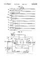
- FIG. 1is a block diagram illustrating an embodiment of the present invention in a battery powered system
- FIG. 2is a detailed circuit diagram illustrating a clock oscillator device according to an embodiment of the present invention
- FIG. 3is a timing diagram illustrating the power ON and subsequent normal operating mode of operation of an embodiment of the present invention
- FIG. 4is a timing diagram illustrating the clock disable mode according to an embodiment of the present invention.
- FIG. 5is a timing diagram for the SLEEP mode according to an embodiment of the present invention.
- FIG. 6is a detailed circuit diagram illustrating a clock oscillator device according to a second embodiment of the present invention.
- FIG. 7is a timing diagram illustrating the power on and subsequent normal operating mode of an operation of the second embodiment of the present invention.
- FIG. 8is a timing diagram illustrating the clock disable mode according to the second embodiment of the present invention.
- FIG. 9is a timing diagram for the sleep mode according to the second embodiment of the present invention.
- FIG. 1is a block diagram showing implementation of a device according to one embodiment of the present invention.
- Logic states0 or 1 are sent through signal lines 10 and 20 to a device 100.
- a synchronous output signalis sent to host 500.
- the elements within the deviceensure that only uniform clock signals are output.
- FIG. 2is a circuit diagram illustrating the basic structure of one embodiment of the present invention.
- the device 100comprises a chip which uses a Transistor-Transistor-Logic (TTL) design.
- TTLTransistor-Transistor-Logic
- CMOScomplementary-metal-oxide-silicon
- the device 100is controlled by a clock output controller 80.
- the clock output controllerincludes input logic circuitry 31, a signal synchronizer 43 and output logic 32.
- the input and output logic circuitrymay comprise OR gates.
- the synchronizer 43comprises D flip-flops, 41 and 42, each having a single D input represented by D 1 and D 2 , respectively.
- a flip-flop output Q1is positive-edge triggered such that it will take on the current state of the D1 input only when the oscillator signal changes from a low to high voltage level.
- the output from Q 1is sent to D 2 .
- Q 2is similarly enabled, at the leading edge of the oscillator signal.
- Flip-flopsare useful in this application because they are bistable, thus producing a steady high or low output.
- the operation of the clock oscillator device of the first embodiment in any modeis substantially as follows.
- a signal from signal line 20reaches the oscillator 25 to generate or stop an oscillator signal.
- the OFF signal from signal line 20also reaches a reset delay circuit 15.
- a quiescent clockexists at logical "1". Both OFF and HALT are at logical 1 when asserted.
- the delay circuit 15may be any conventional device that produces a finite, accurate time delay between a signal imposed on its input and the appearance of the signal at its output.
- the signal from the delay circuit 15is logically ORed with the signal from signal line 10 at OR gate 31.
- OR gate 31is either an asserted DISABLE signal for preventing an oscillating output or a deasserted DISABLE signal for allowing an oscillating output.
- the signalis output at 30 to D flip-flop 41 and subsequently D flip-flop 42.
- the signal from this chain of flip-flopsis output at 50 and is logically ORed with the oscillator signal from signal line 40. The result of this operation is output at 60 to Host 500.
- FIG. 3illustrates a timing diagram a power on operation and the subsequent normal operating mode for the first embodiment.
- Power onis achieved, when a logical "0" is sent through signal line 10.
- the deasserted OFF signalactivates the oscillator 25 and reaches delay circuit 15.
- the delay circuit 15ensures that the oscillator 25 is stable before the uniform output signal is generated.
- the HALT signal and the OFF signalare logically ORed at gate 31 and DISABLE is deasserted.
- the resultant signalis sent through signal line 30 and input to D flip-flop 41 at D 1 . It is then output at Q 1 after the leading edge of the next oscillator signal is received at D 1 .
- the resultis then input to flip-flop 42 at D 2 .
- the output at Q 2follows the input after the next leading edge of the clock pulse.
- the oscillator signal from oscillator 25controls the flip flops 41 and 42 through signal line 40.
- the oscillator signalis logically ORed with the Q 2 output from flip flop 42 at gate 32. Because the Q 2 output follows the D 2 input only after the leading edge of an oscillator signal pulse, when Q 2 is held low, a uniform clock signal (OUT) having no glitches is synchronously enabled as shown by the timing diagram in FIG. 3.
- a pulse widthis represented by t1 and a clock cycle by t2. From FIG. 3 it can be seen that the oscillator signal OSC does not begin with a uniform pulse. However, a delay caused by the reset delay circuit 15 allows the device to be enabled synchronously.
- FIG. 4A resultant timing diagram for the first embodiment of the present invention is shown in FIG. 4.
- the OR gate 31receives the OFF signal from line 20 and the HALT signal from line 10. As a result, the 0R gate generates a DISABLE signal and the D1 input is held high. The Q 1 output remains low until the leading edge of the OSC signal. Thereafter, the Q 1 output also goes high. After being input at D 2 , the synchronizing signal is output at Q 2 after it receives the leading edge of an OSC signal. When a logical "1" from the Q 2 output is ORed with the OSC signal, the non-oscillating output is held high at 60.
- HALTis deasserted.
- the input to OR gate 31goes low.
- the deasserted HALT signal from signal line 10is ORed with the deasserted OFF signal from signal line 20 to produce a low D 1 input.
- the Q 1 outputgoes low only after the leading edge of an oscillator signal pulse.
- the processis repeated at the D 2 input and Q 2 output of D flip-flop 42.
- An output from D flip-flops 41, 42is ORed with the OSC signal at OR gate 32 to output a uniform clock signal having no glitches at 60.
- the OFF signalis asserted while the HALT signal is asserted.
- a timing diagram for the SLEEP mode for the first embodiment of the present inventionis shown in FIG. 5. Upon assertion of the OFF signal, no oscillating signal is generated. When no oscillations occur, significant power savings result.
- the uniform clock output signalis stable from the initial assertion of the HALT signal and produces no asynchronous output.
- FIG. 6A second embodiment of the present invention is illustrated in FIG. 6.
- the circuit of the second embodimentincludes all the features of the first embodiment and also includes several additional features to enhance its reliability.
- HALT and OFF signalsare sent to a clock output controller 180 that includes input logic 131, output logic 132, and signal synchronizer 143.
- a DIEABLE signal 130is sent from input logic 131 to synchronizer 143.
- the synchronizer 143includes first and second O flip-flops 141 and 142 respectively.
- An Oscillator 125supplies its signal to the synchronizer 143 and to output logic 132.
- the second embodimentincludes several features not found in the first embodiment.
- a power on reset circuit 145is connected to both first and second flip flops 141 and 142.
- the reset circuit 145initializes both flip flops prior to any operation of or input to the circuit. This reset operation prevents bad or nonuniform oscillator pulses from resulting in asynchronous clock outputs during power ON.
- the reset circuitis especially important during the initial power ON operation as illustrated in FIG. 7. Glitches are avoided through the addition of the power on reset circuit.
- a second additional feature of the present embodimentis a third input signal line to clock output controller 180.
- the input logicis a three input OR gate 131.
- the third input lineis included to obviate the necessity of continuously asserting HALT during the SLEEP mode.
- the operation of the SLEEP mode for the second embodiment of the present inventionis illustrated in FIG. 9.
- a third additional feature included in the second embodiment of the present inventionis oscillator controller 117.
- the oscillator controllerensures that the oscillator 125 is functioning normally when the clock output is turned on and off.
- the timing diagrams 7-9illustrate the power on, clock disable and SLEEP modes respectively for the second embodiment of the present invention. These modes are substantially similar to those described in relation to the first embodiment.
- the signals described in the first embodimentare identically labeled in the timing diagrams for the second embodiment.
- the additional signals for the power on reset and the OSC offare also appropriately labeled.
- the present inventionproduces a synchronous output whenever a mode change is implemented.
- Two low power stand-by modes, SLEEP and clock disable,are provided by the oscillator-type device of the present invention. By avoiding unnecessary oscillations, the device provides a significant savings of both power and time.
Landscapes
- Physics & Mathematics (AREA)
- Nonlinear Science (AREA)
- Manipulation Of Pulses (AREA)
Abstract
Description
Claims (16)
Priority Applications (1)
| Application Number | Priority Date | Filing Date | Title |
|---|---|---|---|
| US08/532,186US5568100A (en) | 1995-09-22 | 1995-09-22 | Synchronous power down clock oscillator device |
Applications Claiming Priority (1)
| Application Number | Priority Date | Filing Date | Title |
|---|---|---|---|
| US08/532,186US5568100A (en) | 1995-09-22 | 1995-09-22 | Synchronous power down clock oscillator device |
Publications (1)
| Publication Number | Publication Date |
|---|---|
| US5568100Atrue US5568100A (en) | 1996-10-22 |
Family
ID=24120715
Family Applications (1)
| Application Number | Title | Priority Date | Filing Date |
|---|---|---|---|
| US08/532,186Expired - LifetimeUS5568100A (en) | 1995-09-22 | 1995-09-22 | Synchronous power down clock oscillator device |
Country Status (1)
| Country | Link |
|---|---|
| US (1) | US5568100A (en) |
Cited By (9)
| Publication number | Priority date | Publication date | Assignee | Title |
|---|---|---|---|---|
| US5821826A (en)* | 1996-06-17 | 1998-10-13 | Burr-Brown Corporation | Oscillator circuit synchronization |
| US5903601A (en)* | 1996-12-17 | 1999-05-11 | Texas Instruments Incorporated | Power reduction for UART applications in standby mode |
| US5912570A (en)* | 1997-01-08 | 1999-06-15 | Nokia Mobile Phones Limited | Application specific integrated circuit (ASIC) having improved reset deactivation |
| EP1102391A3 (en)* | 1999-11-18 | 2002-02-06 | Seiko Epson Corporation | Piezoelectric oscillator and electronic device using it |
| US6720673B2 (en)* | 2001-04-11 | 2004-04-13 | International Business Machines Corporation | Voltage island fencing |
| US20050285689A1 (en)* | 2004-06-24 | 2005-12-29 | Jeng-Huang Wu | Crystal oscillator circuit with activation control |
| US20060226891A1 (en)* | 2005-04-08 | 2006-10-12 | Hynix Semiconductor Inc. | Voltage pumping device |
| US7310760B1 (en) | 2002-12-11 | 2007-12-18 | Chung Sun | Apparatus and method for initializing an integrated circuit device and activating a function of the device once an input power supply has reached a threshold voltage |
| US20100214854A1 (en)* | 2009-02-23 | 2010-08-26 | Samsung Electronics Co., Ltd. | Shift register providing glitch free operation in power saving mode |
Citations (6)
| Publication number | Priority date | Publication date | Assignee | Title |
|---|---|---|---|---|
| US3947697A (en)* | 1973-09-28 | 1976-03-30 | International Standard Electric Corporation | Synchronizing circuit including two flip-flops and circuit means to protect a synchronized signal from an unstable state of the flip-flops |
| US4641044A (en)* | 1984-01-25 | 1987-02-03 | Kabushiki Kaisha Toshiba | Clock generator with reset and initialization circuitry |
| US4864255A (en)* | 1986-09-09 | 1989-09-05 | Nec Corporation | Oscillator capable of quickly supplying a stable oscillation signal |
| US5225723A (en)* | 1990-05-24 | 1993-07-06 | Apple Computer, Inc. | Circuitry for the timing data output enable pulses |
| US5369311A (en)* | 1992-03-06 | 1994-11-29 | Intel Corporation | Clock generator control circuit |
| US5440250A (en)* | 1993-06-26 | 1995-08-08 | Deutsche Itt Industries Gmbh | Clock-generating circuit for clock-controlled logic circuits |
- 1995
- 1995-09-22USUS08/532,186patent/US5568100A/ennot_activeExpired - Lifetime
Patent Citations (6)
| Publication number | Priority date | Publication date | Assignee | Title |
|---|---|---|---|---|
| US3947697A (en)* | 1973-09-28 | 1976-03-30 | International Standard Electric Corporation | Synchronizing circuit including two flip-flops and circuit means to protect a synchronized signal from an unstable state of the flip-flops |
| US4641044A (en)* | 1984-01-25 | 1987-02-03 | Kabushiki Kaisha Toshiba | Clock generator with reset and initialization circuitry |
| US4864255A (en)* | 1986-09-09 | 1989-09-05 | Nec Corporation | Oscillator capable of quickly supplying a stable oscillation signal |
| US5225723A (en)* | 1990-05-24 | 1993-07-06 | Apple Computer, Inc. | Circuitry for the timing data output enable pulses |
| US5369311A (en)* | 1992-03-06 | 1994-11-29 | Intel Corporation | Clock generator control circuit |
| US5440250A (en)* | 1993-06-26 | 1995-08-08 | Deutsche Itt Industries Gmbh | Clock-generating circuit for clock-controlled logic circuits |
Cited By (18)
| Publication number | Priority date | Publication date | Assignee | Title |
|---|---|---|---|---|
| US5821826A (en)* | 1996-06-17 | 1998-10-13 | Burr-Brown Corporation | Oscillator circuit synchronization |
| US5903601A (en)* | 1996-12-17 | 1999-05-11 | Texas Instruments Incorporated | Power reduction for UART applications in standby mode |
| US5912570A (en)* | 1997-01-08 | 1999-06-15 | Nokia Mobile Phones Limited | Application specific integrated circuit (ASIC) having improved reset deactivation |
| EP0854578A3 (en)* | 1997-01-08 | 2002-01-16 | Nokia Mobile Phones Ltd. | Application specific integrated circuit (asic) having improved reset deactivation |
| EP1102391A3 (en)* | 1999-11-18 | 2002-02-06 | Seiko Epson Corporation | Piezoelectric oscillator and electronic device using it |
| US6480071B1 (en) | 1999-11-18 | 2002-11-12 | Seiko Epson Corporation | Piezoelectric oscillator and electronic device |
| US6720673B2 (en)* | 2001-04-11 | 2004-04-13 | International Business Machines Corporation | Voltage island fencing |
| US7310760B1 (en) | 2002-12-11 | 2007-12-18 | Chung Sun | Apparatus and method for initializing an integrated circuit device and activating a function of the device once an input power supply has reached a threshold voltage |
| US7673194B1 (en) | 2002-12-11 | 2010-03-02 | Actel Corporation | Apparatus and method for initializing an integrated circuit device and activating a function of the device once an input power supply has reached a threshold voltage |
| US7426667B1 (en) | 2002-12-11 | 2008-09-16 | Actel Corporation | Apparatus and method for initializing an integrated circuit device and activating a function of the device once an input power supply has reached a threshold voltage |
| US7057468B2 (en)* | 2004-06-24 | 2006-06-06 | Faraday Technology Corp. | Crystal oscillator circuit with activation control |
| US20050285689A1 (en)* | 2004-06-24 | 2005-12-29 | Jeng-Huang Wu | Crystal oscillator circuit with activation control |
| US7345525B2 (en) | 2005-04-08 | 2008-03-18 | Hynix Semiconductor Inc. | Voltage pumping device |
| US20080111613A1 (en)* | 2005-04-08 | 2008-05-15 | Hynix Semiconductor Inc. | Voltage Pumping Device |
| US20060226891A1 (en)* | 2005-04-08 | 2006-10-12 | Hynix Semiconductor Inc. | Voltage pumping device |
| US7518433B2 (en) | 2005-04-08 | 2009-04-14 | Hynix Semiconductor Inc. | Voltage pumping device |
| US20100214854A1 (en)* | 2009-02-23 | 2010-08-26 | Samsung Electronics Co., Ltd. | Shift register providing glitch free operation in power saving mode |
| US8199589B2 (en) | 2009-02-23 | 2012-06-12 | Samsung Electronics Co., Ltd. | Shift register providing glitch free operation in power saving mode |
Similar Documents
| Publication | Publication Date | Title |
|---|---|---|
| US5315181A (en) | Circuit for synchronous, glitch-free clock switching | |
| EP1451666B1 (en) | Glitch free clock selection switch | |
| US5550489A (en) | Secondary clock source for low power, fast response clocking | |
| KR100379766B1 (en) | Pll system clock generator with instantaneous clock frequency shifting | |
| US5623234A (en) | Clock system | |
| US5764710A (en) | Meta-stable-resistant front-end to a synchronizer with asynchronous clear and asynchronous second-stage clock selector | |
| US5790609A (en) | Apparatus for cleanly switching between various clock sources in a data processing system | |
| US5903746A (en) | Apparatus and method for automatically sequencing clocks in a data processing system when entering or leaving a low power state | |
| US6563349B2 (en) | Multiplexor generating a glitch free output when selecting from multiple clock signals | |
| US6819150B1 (en) | Method and apparatus for quick clock swapping using much slower asynchronous clock for power savings | |
| US5915107A (en) | Cross clock domain clocking for a system using two clock frequencies where one frequency is fractional multiple of the other | |
| WO1998056113A1 (en) | Digital delay lock loop | |
| US6989695B2 (en) | Apparatus and method for reducing power consumption by a data synchronizer | |
| US5903601A (en) | Power reduction for UART applications in standby mode | |
| US5568100A (en) | Synchronous power down clock oscillator device | |
| US5794019A (en) | Processor with free running clock with momentary synchronization to subsystem clock during data transfers | |
| US4870299A (en) | Dynamic switching circuit for multiple asynchronous clock sources | |
| US7109776B2 (en) | Gating for dual edge-triggered clocking | |
| US5625311A (en) | System clock generating circuit having a power saving mode capable of maintaining a satisfactory processing speed | |
| US20120306585A1 (en) | Oscillators with low power mode of operation | |
| US7003683B2 (en) | Glitchless clock selection circuit | |
| US5414745A (en) | Synchronized clocking disable and enable circuit | |
| US4825407A (en) | Method and circuit for controlling single chip microcomputer | |
| US6292038B1 (en) | Smooth clock switching for power managed PCI adapters | |
| US5799177A (en) | Automatic external clock detect and source select circuit |
Legal Events
| Date | Code | Title | Description |
|---|---|---|---|
| AS | Assignment | Owner name:AT&T CORP., NEW YORK Free format text:ASSIGNMENT OF ASSIGNORS INTEREST;ASSIGNOR:LOCANTHI, BART N.;REEL/FRAME:007686/0047 Effective date:19950911 | |
| STCF | Information on status: patent grant | Free format text:PATENTED CASE | |
| AS | Assignment | Owner name:LUCENT TECHNOLOGIES, INC., NEW JERSEY Free format text:ASSIGNMENT OF ASSIGNORS INTEREST;ASSIGNOR:AT&T CORP.;REEL/FRAME:008102/0142 Effective date:19960329 | |
| FEPP | Fee payment procedure | Free format text:PAYOR NUMBER ASSIGNED (ORIGINAL EVENT CODE: ASPN); ENTITY STATUS OF PATENT OWNER: LARGE ENTITY | |
| FPAY | Fee payment | Year of fee payment:4 | |
| FPAY | Fee payment | Year of fee payment:8 | |
| FPAY | Fee payment | Year of fee payment:12 | |
| AS | Assignment | Owner name:DEUTSCHE BANK AG NEW YORK BRANCH, AS COLLATERAL AG Free format text:PATENT SECURITY AGREEMENT;ASSIGNORS:LSI CORPORATION;AGERE SYSTEMS LLC;REEL/FRAME:032856/0031 Effective date:20140506 | |
| AS | Assignment | Owner name:AVAGO TECHNOLOGIES GENERAL IP (SINGAPORE) PTE. LTD Free format text:ASSIGNMENT OF ASSIGNORS INTEREST;ASSIGNOR:AGERE SYSTEMS LLC;REEL/FRAME:035365/0634 Effective date:20140804 | |
| AS | Assignment | Owner name:AGERE SYSTEMS LLC, PENNSYLVANIA Free format text:TERMINATION AND RELEASE OF SECURITY INTEREST IN PATENT RIGHTS (RELEASES RF 032856-0031);ASSIGNOR:DEUTSCHE BANK AG NEW YORK BRANCH, AS COLLATERAL AGENT;REEL/FRAME:037684/0039 Effective date:20160201 Owner name:LSI CORPORATION, CALIFORNIA Free format text:TERMINATION AND RELEASE OF SECURITY INTEREST IN PATENT RIGHTS (RELEASES RF 032856-0031);ASSIGNOR:DEUTSCHE BANK AG NEW YORK BRANCH, AS COLLATERAL AGENT;REEL/FRAME:037684/0039 Effective date:20160201 |