US5568062A - Low noise tri-state output buffer - Google Patents
Low noise tri-state output bufferDownload PDFInfo
- Publication number
- US5568062A US5568062AUS08/502,531US50253195AUS5568062AUS 5568062 AUS5568062 AUS 5568062AUS 50253195 AUS50253195 AUS 50253195AUS 5568062 AUS5568062 AUS 5568062A
- Authority
- US
- United States
- Prior art keywords
- pull
- input
- output
- transistors
- voltage
- Prior art date
- Legal status (The legal status is an assumption and is not a legal conclusion. Google has not performed a legal analysis and makes no representation as to the accuracy of the status listed.)
- Expired - Lifetime
Links
Images
Classifications
- H—ELECTRICITY
- H03—ELECTRONIC CIRCUITRY
- H03K—PULSE TECHNIQUE
- H03K19/00—Logic circuits, i.e. having at least two inputs acting on one output; Inverting circuits
- H03K19/003—Modifications for increasing the reliability for protection
- H03K19/00346—Modifications for eliminating interference or parasitic voltages or currents
- H03K19/00361—Modifications for eliminating interference or parasitic voltages or currents in field effect transistor circuits
- H—ELECTRICITY
- H03—ELECTRONIC CIRCUITRY
- H03K—PULSE TECHNIQUE
- H03K17/00—Electronic switching or gating, i.e. not by contact-making and –breaking
- H03K17/16—Modifications for eliminating interference voltages or currents
- H03K17/161—Modifications for eliminating interference voltages or currents in field-effect transistor switches
- H03K17/165—Modifications for eliminating interference voltages or currents in field-effect transistor switches by feedback from the output circuit to the control circuit
- H03K17/166—Soft switching
- H03K17/167—Soft switching using parallel switching arrangements
- H—ELECTRICITY
- H03—ELECTRONIC CIRCUITRY
- H03K—PULSE TECHNIQUE
- H03K19/00—Logic circuits, i.e. having at least two inputs acting on one output; Inverting circuits
- H03K19/02—Logic circuits, i.e. having at least two inputs acting on one output; Inverting circuits using specified components
- H03K19/08—Logic circuits, i.e. having at least two inputs acting on one output; Inverting circuits using specified components using semiconductor devices
- H03K19/094—Logic circuits, i.e. having at least two inputs acting on one output; Inverting circuits using specified components using semiconductor devices using field-effect transistors
- H03K19/09425—Multistate logic
- H03K19/09429—Multistate logic one of the states being the high impedance or floating state
Definitions
- the present inventionrelates to electronic digital logic circuitry for interfacing, i.e. buffering logic signals, between different circuit elements, for example between on-chip circuitry and conductive traces on a printed circuit board leading to other integrated circuit chips.
- the inventionparticularly relates to buffer circuits with input noise rejection and output switching noise reduction.
- Conventional buffer circuitsinclude a single input translator, i.e. level shifter, that receives an input signal with TTL logic levels (0 V is low, 3.0 V is high) and that translates that signal to CMOS logic levels (0 V is low, 5.0 V is high). In both cases the nominal transition point is 1.5 V.
- This translated signalis then reinverted through a CMOS inverter, since the translator usually has an inverting as well as translating function, and then goes through a set of logic gates.
- the logic gatesinclude a disable input so that a high impedance state can be asserted if desired.
- the set of logic gatesthen drives pull-up and pull-down output transistors connected to an output line.
- One problem with such buffer circuitsis that of noise generation.
- While the input signalhas a relatively slow ramp rate (3 V/2.5 ns), by the time the signal has made successive transitions in the translator, inverter and logic gates, the ramp rate is approximately 8 times higher (5 V/0.5 ns). This causes the output transistors to open and close quickly, which produces ground bounce or overshoot of the output signal due to the inductance between the integrated circuit chip's internal ground and power supply and external ground and power supply.
- the buffer circuitalso has a relatively slow throughput time due to the many layers of logic between the input and output of the circuit. An ideal buffer would be relatively fast and yet would linearly ramp its output current to a maximum to reduce ground bounce or overshoot and then linearly ramp down its output current to source small DC current sufficient to maintain the final voltage on the output line. It would also reject input noise spikes instead of transmitting them to the output.
- An object of the present inventionis to provide a buffer circuit which is faster, rejects input noise spikes and does not generate noise at the output, and which has low power dissipation.
- a low noise fast buffer circuithaving dual tristate input translators in parallel driving a pull-up transistor and a pull-down transistor, respectively with means for shutting off these pull-up and pull-down transistors when the input translators are tristated.
- Tristate input translators, inverters and buffershave both high and low output states and also a third high impedance state. These circuit elements are said to be "tristated", i.e. placed in their high impedance state, by a separate control signal input.)
- the circuitincludes a parallel set of pull-up and pull-down transistors that also receive tristatable inputs through another pair of input translators.
- Feedback meansshut off at least one of the pull-up transistors during a low-to-high transition after a logic high transition voltage has been reached at the output, and similarly shut off at least one of the pull-down transistors during a high-to-low transition after a logic low transition voltage has been reached at the output. This prevents overshoot or undershoot of the output.
- the circuitfilters out unwanted input noise spikes, because the input translators drive the pull-up and pull-down transistors with a relatively slow ramp rate, so that spikes of less than 1 nsec duration and less than 1.8 V peaks do not turn the transistors on sufficiently to pull the output through the transition point.
- the buffer circuitis also fast, because the input translators drive the pull-up and pull-down transistors directly, rather than through several stages of logic gates.
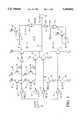
- FIG. 1is a schematic circuit diagram of a buffer circuit of the present invention.
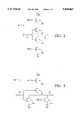
- FIG. 2is a schematic transistor level diagram of an input translator circuit element used in the buffer circuit of FIG. 1.
- FIG. 3is a schematic transistor level diagram of a NOR gate used in the feedback portion of the buffer circuit of FIG. 1.
- a buffer circuit of the present inventionincludes a first pull-up transistor 11, a second pull-up transistor 13, a first pull-down transistor 15, and a second pull-down transistor 17. All four of these transistors are field-effect transistors connected to an output line 19 to form the output transistors that drive an output terminal 20 of the circuit.
- the pull-up transistors 11 and 13are also connected to a first voltage supply line V dd
- the pull-down transistors 15 and 17are connected to a second voltage supply line V ss .
- the second voltage line V ssis defined as being at the reference or ground voltage (0 V)
- the first voltage line V ddis at +5 V.
- the two pull-down transistors 15 and 17are n-channel devices, while the second pull-up transistor 13 is a p-channel device.
- the first pull-up transistor 11is preferably an n-channel device with a CMOS inverter 21 between the input stage of the circuit and the control gate of transistor 11.
- the use of an n-channel device for pull-up transistor 11minimizes power dissipation for reasons that will be discussed below.
- the input terminal 22 of the buffer circuitconnects in parallel to four tristate inverting input translators 23, 25, 27 and 29, with a separate translator being provided for driving each one of the four output transistors 11, 13, 15 and 17 respectively.
- Pull-up transistors 31 and 33are connected at nodes 32 and 34 between the outputs of input translators 23 and 25 and the inputs of output transistors 11 and 13.
- the node 32communicates only indirectly with the gate of transistor 11 via inverter 21.
- Pull-down transistors 35 and 37are connected at nodes 36 and 38 between the outputs of input translators 27 and 29 and the inputs of output transistors 15 and 17.
- Transistors 31 and 33are p-channel devices connected to first voltage supply line V dd , while transistors 35 and 37 are n-channel devices connected to second voltage supply line V ss .
- Transistors 31, 33, 35 and 37are driven by control signals OE, S1, OE, and S2 applied to their gates that cause their corresponding output transistors 11, 13, 15 and 17 to turn off when the input translators 23, 25, 27 and 29 are placed in a high impedance state by related control signals OE, S1, OE and S2.
- the input translators 23, 25, 27 and 29are typically sized to all have a 1.5 V transition voltage, which is the nominal transition voltage for TTL logic.
- the input translators 23 and 25 that drive the pull-up output transistors 11 and 13may be sized to have a smaller transition point somewhere between 0.8 V and 1.5 V, for example, 1.2 V, while the input transistors 27 and 29 that drive the pull-down output transistors 15 and 17 may be sized to have a larger transition point somewhere between 1.5 V and 2.0 V, for example 1.8 V.
- the translators 23 and 27 driving the weaker output transistors 11 and 15, which are mainly used to complete a transition and maintain the output level after the finish of a transitionmay have a 1.5 V transition voltage, while only the translators 25 and 29 driving the stronger output transistors 13 and 17 have different transition voltages as described above.
- the circuitminimizes the generation of noise at the output by avoiding ground bounce.
- the input signal received at the input terminal 22normally has a relatively slow ramp rate of about 3 V/2.5 ns. However, in conventional buffers by the time the signal has traversed the logic gates to reach the gates of the output transistors, the ramp rate has increased substantially to about 5 V/0.5 ns. This causes the output transistors to open and close quickly, leading to a rapid change in current flow (dI/dt) and ground bounce proportional to L ⁇ dI/dt, where L is the inductance between the circuit's ground V ss and an external ground.
- the input translatorsoperate as linear inverting amplifiers, where the output has a transition rate proportional to and at most two times higher than that at its input.
- Signal transitions of about 2.25 V/nsdrive the output transistors 13, 15 and 17.
- the transistor 11is driven by the inverter 21, whose output ramp is also slow because of its small size in relation to the load it drives.
- the relative size of the output transistors to the input translatorsis chosen to ensure that the slow transition is maintained by the output transistors.
- the slow turn on or turn off of the output transistorsresults in a slow change in current flow (small dI/dt), thereby minimizing ground bounce. Note that the slower transition rates are more than compensated for by the shorter throughput time achieved by the fewer logic levels traversed by the signal.
- the buffer circuituses a tristate input translator that includes an inverter element 41 with a p-channel pull-up transistor 43 and an n-channel pull-down transistor 45, and two n-channel transistors 47 and 49 connecting the inverter element 41 to the respective first and second voltage supply lines V dd and V ss .
- the transistors 47 and 49both have an enable control signal EN applied to their gates.
- the relative strengths or saturation currents of the pull-up and pull-down transistorsdetermine the nominal transition voltage as well as the ramp rate of the output. While the transistor sizes (channel widths and lengths) are process dependent, representative size values for a 1.5 V transition level for TTL input signals and a low ramp rate are 12/0.8 (channel width/channel length in microns) for n-channel transistor 47, 18/0.8 for p-channel transistor 43, and 9/0.8 for both n-channel pull-down transistors 45 and 49. The sizes will differ for translators with other transition levels. If n-channel transistor 47 is replaced by a p-channel transistor so as to pull the output 53 all the way up to V dd instead of just to 3 V, that transistor would have the same 18/0.8 size as transistor 43.
- the CMOS inverter 21has p-channel and n-channel transistors whose sizes may both be 19.5/0.8. Transistor 11 is turned on very slowly due to the weak pull-up of inverter 21.
- representative effective sizes using the same transistor processare 700/0.8 for n-channel transistor 11, 620/0.8 for p-channel transistor 13, 120/0.8 for n-channel transistor 15 and 680/0.8 for n-channel transistor 17.
- Each of these output transistorsmay be formed by a set of parallel transistors all sized at about 20/0.8.
- transistor 11could be formed by 35 of such parallel transistors.
- the buffer circuitIn addition to avoiding the generation of noise from ground bounce, the buffer circuit also filters out any unwanted input spikes. This can be understood by considering an input transition from low to high. By the time the input signal has risen to 1.8 V, the outputs of the input translators will have fallen only from 5 V to 3.5 V. While this starts the opening of at least the pull-up transistor 13 and the closing of the pull-down transistor 15, neither of these transistors is fully open or shut yet, and the output 20 will not have moved through the transition point, i.e. have dropped below 2.0 V. By contrast, conventional buffers will usually have switched at this point, with their logic outputs fully low and their p-channel pull-up and n-channel pull-down output transistors fully open and shut, respectively.
- the circuit of the present inventionwill reject a 1 ns wide input noise spike from 0 V to 1.8 V (or from 3.0 V to 1.2 V) without producing a corresponding spike transition at the output. That is, the output will not rise above 0.8 V (the upper limit of a low logic value) or drop below 2.0 V (the lower limit of a high logic value) when such 1.8 V spikes are received at the input 22.
- the buffer circuit in FIG. 1includes a pair of feedback elements 61 and 63 responsive to the voltage level on the output terminal 20 for controlling the state of two of the output transistors 13 and 17.
- the feedback element 61includes a NOR gate 65 with one input connected to the output line 19 and another input connected to receive a disable signal OE.
- An inverter 67 with a weak pull-up transistor 69is connected to the output of NOR gate 65.
- the NOR gatehas a transition point of about 2.2 V. When the output 20 exceeds this transition point, control signal S1 on the output of NOR gate 65 is low and control signal S1 on the output of inverter 67 is high, tristating the input translator 25 and shutting off output transistor 13.
- the feedback element 63includes an inverter 71 connecting the output line 19 of the buffer circuit to an input of another NOR gate 73. Another input of the NOR gate 73 receives a disable signal OE. A second inverter 75 with a weak pull-up transistor 77 is connected to the output of the NOR gate 73.
- the inverter 71has a transition point of 1.0 V. When the output 20 drops below this transition point, control signal S2 on the output of the second inverter 75 is high, tristating the input translator 29 and shutting off output transistor 17. Second pull-down transistor 17 is much larger than first pull-down transistor 15 (about 6 ⁇ larger) and is big enough to pull the output line 19 down rapidly.
- Transistor 17is enabled when the output is high, but is then switched off by control signal 52 when the output falls below 1.0 V.
- Transistor 15is used to complete the pull-down of the output at a slow enough rate to avoid undershoot and then to provide the current sink needed to keep the output low.
- second pull-up transistor 13is stronger than first pull-up transistor 11 and is used to pull the output line 19 up rapidly until the output exceeds 2.2 V. Then control signals S1 and S1 shut the transistor 13 off.
- Transistor 11completes the pull-up (to about 3.0 V) and sustains the high output level.
- the buffer circuituses n-channel pull-up transistors 47 in its translators to reduce leakage current.
- One problem with conventional translators that use a p-channel transistor in that locationis that they leak current whenever the input level is between 3 V and 4 V.
- V dd5 V
- both p-channel pull-up transistors and both n-channel pull-down transistorsare partially conducting.
- the use of an n-channel pull-up device 47causes the node between the pull-up devices 47 and 43 to be a threshold drop below V dd , i.e. about 4 V, and so leakage current through the p-channel device 43 is about 75% less.
- the use of an n-channel pull-up device 11 for one of the output transistorsreduces power dissipation as the output line 19 transitions between low (0 V) and high (preferably above 3.4 V).
- the power needed to cause such transitions in a capacitive circuitis CV 2 f, where C is the capacitance of the circuit, V is the voltage change, and f is the frequency.
- the capacitance Cis made up of components from the trace on the printed circuit board to which the chip is connected and that from the pins connecting the chip to the trace. Power dissipation is minimized when the voltage swing is limited to not more than 3.8 V.
- p-channel pull-up transistor 13starts pulling the output up and then is switched off by control signals S1 and S1 when the input level rises above about 2.2 V. Then n-channel transistor 11 completes the pull-up. However, because it is an n-channel device, it can only pull it up to a threshold drop below V dd , i.e. about 3.8 V. Accordingly, power consumption is minimized by the limited voltage swing. Alternatively, if CMOS output levels are desired, a p-channel transistor must be used in place of transistor 11 in order to pull the output line 19 all the way up to the power supply voltage V dd .
- a NOR gate 65 with 2.2 V transition voltageincludes series pull-up transistors 81 and 83 and parallel pull-down transistors 85 and 87.
- One pull-up and one pull-down transistor 81 and 85are connected to the input 89, while the other transistors 83 and 87 received enable control signals OE and OE for when the buffer is tristated.
- the pull-up transistor 83 closest to the power supply line V ddis an n-channel device to provide a threshold drop to reduce power consumption by p-channel pull-up transistor 81.
- Typical process dependent transistor sizesare 22.5/0.8 for transistor 83, 16/0.8 for transistor 81, 25/0.8 for transistor 85 ad 8/0.8 for transistor 87.
- the buffer circuit of the present inventionis thus seen to be fast, have low power consumption, reduced ground bounce or overshoot of the output signal, and input noise spike rejection.
Landscapes
- Engineering & Computer Science (AREA)
- Physics & Mathematics (AREA)
- Computer Hardware Design (AREA)
- Computing Systems (AREA)
- General Engineering & Computer Science (AREA)
- Mathematical Physics (AREA)
- Power Engineering (AREA)
- Logic Circuits (AREA)
Abstract
Description
Claims (8)
Priority Applications (4)
| Application Number | Priority Date | Filing Date | Title |
|---|---|---|---|
| US08/502,531US5568062A (en) | 1995-07-14 | 1995-07-14 | Low noise tri-state output buffer |
| JP9506688AJPH11509391A (en) | 1995-07-14 | 1996-06-26 | Low noise tri-state output buffer |
| PCT/US1996/010980WO1997004528A1 (en) | 1995-07-14 | 1996-06-26 | Low noise tri-state output buffer |
| EP96923489AEP0839409A4 (en) | 1995-07-14 | 1996-06-26 | Low noise tri-state output buffer |
Applications Claiming Priority (1)
| Application Number | Priority Date | Filing Date | Title |
|---|---|---|---|
| US08/502,531US5568062A (en) | 1995-07-14 | 1995-07-14 | Low noise tri-state output buffer |
Publications (1)
| Publication Number | Publication Date |
|---|---|
| US5568062Atrue US5568062A (en) | 1996-10-22 |
Family
ID=23998245
Family Applications (1)
| Application Number | Title | Priority Date | Filing Date |
|---|---|---|---|
| US08/502,531Expired - LifetimeUS5568062A (en) | 1995-07-14 | 1995-07-14 | Low noise tri-state output buffer |
Country Status (4)
| Country | Link |
|---|---|
| US (1) | US5568062A (en) |
| EP (1) | EP0839409A4 (en) |
| JP (1) | JPH11509391A (en) |
| WO (1) | WO1997004528A1 (en) |
Cited By (66)
| Publication number | Priority date | Publication date | Assignee | Title |
|---|---|---|---|---|
| US5767696A (en)* | 1995-11-03 | 1998-06-16 | Samsung Electronics Co., Ltd. | Tri-state devices having exclusive gate output control |
| US5864872A (en)* | 1989-05-15 | 1999-01-26 | Dallas Semiconductor Corporation | Single wire communication system |
| US5877647A (en)* | 1995-10-16 | 1999-03-02 | Texas Instruments Incorporated | CMOS output buffer with slew rate control |
| US5896338A (en)* | 1997-04-11 | 1999-04-20 | Intel Corporation | Input/output power supply detection scheme for flash memory |
| US5903500A (en)* | 1997-04-11 | 1999-05-11 | Intel Corporation | 1.8 volt output buffer on flash memories |
| US5933026A (en)* | 1997-04-11 | 1999-08-03 | Intel Corporation | Self-configuring interface architecture on flash memories |
| US5969541A (en)* | 1997-05-19 | 1999-10-19 | Stmicroelectronics, Inc. | Current inhibiting I/O buffer having a 5 volt tolerant input and method of inhibiting current |
| US6133757A (en)* | 1998-07-16 | 2000-10-17 | Via Technologies, Inc. | High-speed and low-noise output buffer |
| US6137319A (en)* | 1999-04-30 | 2000-10-24 | Intel Corporation | Reference-free single ended clocked sense amplifier circuit |
| US6177810B1 (en)* | 1998-12-17 | 2001-01-23 | Siemens Aktiengesellschaft | Adjustable strength driver circuit and method of adjustment |
| US6201428B1 (en)* | 1999-03-18 | 2001-03-13 | Intel Corporation | 5-volt tolerant 3-volt drive push-pull buffer/driver |
| US6204696B1 (en)* | 1998-09-22 | 2001-03-20 | Intel Corporation | Domino circuits with high performance and high noise immunity |
| US6225826B1 (en) | 1998-12-23 | 2001-05-01 | Intel Corporation | Single ended domino compatible dual function generator circuits |
| US6271713B1 (en) | 1999-05-14 | 2001-08-07 | Intel Corporation | Dynamic threshold source follower voltage driver circuit |
| US6275071B1 (en) | 1999-12-29 | 2001-08-14 | Intel Corporation | Domino logic circuit and method |
| US6316960B2 (en) | 1999-04-06 | 2001-11-13 | Intel Corporation | Domino logic circuit and method |
| US6323672B1 (en)* | 1997-06-25 | 2001-11-27 | Sun Microsystems, Inc. | Apparatus for reducing reflections when using dynamic termination logic signaling |
| US6348812B1 (en)* | 2000-07-05 | 2002-02-19 | Elan Research | Dynamic programmable logic array that can be reprogrammed and a method of use |
| EP1211807A1 (en)* | 2000-11-29 | 2002-06-05 | Phoenix Contact GmbH & Co. KG | Digital level adaptation circuit |
| US6404234B1 (en) | 2001-05-09 | 2002-06-11 | Intel Corporation | Variable virtual ground domino logic with leakage control |
| US6476637B1 (en)* | 1999-05-12 | 2002-11-05 | Sharp Kabushiki Kaisha | Voltage level shifter and display device |
| US6486706B2 (en) | 2000-12-06 | 2002-11-26 | Intel Corporation | Domino logic with low-threshold NMOS pull-up |
| US6492837B1 (en)* | 2000-03-17 | 2002-12-10 | Intel Corporation | Domino logic with output predischarge |
| US6529045B2 (en)* | 1999-09-28 | 2003-03-04 | Intel Corporation | NMOS precharge domino logic |
| US6529861B1 (en) | 1999-07-02 | 2003-03-04 | Intel Corporation | Power consumption reduction for domino circuits |
| US6531892B2 (en)* | 2000-09-05 | 2003-03-11 | Xilinx Inc. | Bias voltage generator usable with circuit for producing low-voltage differential signals |
| GB2380624A (en)* | 2001-08-30 | 2003-04-09 | Micron Technology Inc | A logic level translator with prevention of concurrent pull-up and pull-down conduction |
| US6556962B1 (en) | 1999-07-02 | 2003-04-29 | Intel Corporation | Method for reducing network costs and its application to domino circuits |
| EP1306975A1 (en)* | 2001-10-29 | 2003-05-02 | STMicroelectronics S.r.l. | Low-noise output buffer |
| US6570405B1 (en) | 2001-12-20 | 2003-05-27 | Integrated Device Technology, Inc. | Integrated output driver circuits having current sourcing and current sinking characteristics that inhibit power bounce and ground bounce |
| US6617892B2 (en) | 1998-09-18 | 2003-09-09 | Intel Corporation | Single ended interconnect systems |
| US6628552B1 (en) | 1997-04-11 | 2003-09-30 | Intel Corporation | Self-configuring input buffer on flash memories |
| US6694444B1 (en)* | 2000-06-30 | 2004-02-17 | Intel Corporation | System and method for reducing over-shoot and ringback by delaying input and establishing a synchronized pulse over which clamping is applied |
| US20040034844A1 (en)* | 2002-08-15 | 2004-02-19 | Fulcrum Microsystems, Inc. | Methods and apparatus for facilitating physical synthesis of an integrated circuit design |
| US6741098B2 (en)* | 1999-11-25 | 2004-05-25 | Texas Instruments Incorporated | High speed semiconductor circuit having low power consumption |
| US6777975B1 (en)* | 1999-11-30 | 2004-08-17 | Intel Corporation | Input-output bus interface to bridge different process technologies |
| US6873196B2 (en)* | 2001-08-02 | 2005-03-29 | Agilent Technologies, Inc. | Slew rate control of output drivers using FETs with different threshold voltages |
| GB2410632A (en)* | 2001-08-30 | 2005-08-03 | Micron Technology Inc | Combined dynamic logic gate and level shifter and method employing same |
| US20060170638A1 (en)* | 2002-12-20 | 2006-08-03 | Koninklijke Philips Electronics N.V. | Video driver with integrated sample-and-hold amplifier and column buffer |
| US20060226875A1 (en)* | 2005-04-06 | 2006-10-12 | Nec Electronics Corporation | Level shifter circuit |
| US20070250652A1 (en)* | 2006-04-24 | 2007-10-25 | Atmel Corporation | High speed dual-wire communications device requiring no passive pullup components |
| US20080024162A1 (en)* | 2006-07-25 | 2008-01-31 | Stmicroelectronics Pvt. Ltd. | Constant impedance cmos output buffer |
| US20080106298A1 (en)* | 2003-10-28 | 2008-05-08 | Bales Tim J | MOS linear region impedance curvature correction |
| US7471113B1 (en)* | 2006-09-26 | 2008-12-30 | Marvell International Ltd. | Low crowbar current slew rate controlled driver |
| US7498839B1 (en) | 2004-10-22 | 2009-03-03 | Xilinx, Inc. | Low power zones for programmable logic devices |
| US7498836B1 (en) | 2003-09-19 | 2009-03-03 | Xilinx, Inc. | Programmable low power modes for embedded memory blocks |
| US7498835B1 (en) | 2005-11-04 | 2009-03-03 | Xilinx, Inc. | Implementation of low power standby modes for integrated circuits |
| US7504854B1 (en)* | 2003-09-19 | 2009-03-17 | Xilinx, Inc. | Regulating unused/inactive resources in programmable logic devices for static power reduction |
| US7549139B1 (en) | 2003-09-19 | 2009-06-16 | Xilinx, Inc. | Tuning programmable logic devices for low-power design implementation |
| US7562332B1 (en) | 2003-09-19 | 2009-07-14 | Xilinx, Inc. | Disabling unused/inactive resources in programmable logic devices for static power reduction |
| US7581124B1 (en) | 2003-09-19 | 2009-08-25 | Xilinx, Inc. | Method and mechanism for controlling power consumption of an integrated circuit |
| US20090278568A1 (en)* | 2008-05-08 | 2009-11-12 | Texas Instruments Incorporated | Method and system to reduce electromagnetic radiation from semiconductor devices |
| US20110148475A1 (en)* | 2009-12-17 | 2011-06-23 | Phison Electronics Corp. | Driving circuit of input/output interface |
| CN102522950A (en)* | 2012-01-06 | 2012-06-27 | 美商威睿电通公司 | Electronic chip with output signal slew rate control function |
| US20120293204A1 (en)* | 2011-05-20 | 2012-11-22 | Semiconductor Energy Laboratory Co., Ltd. | Semiconductor device |
| US20120293208A1 (en)* | 2011-05-20 | 2012-11-22 | Semiconductor Energy Laboratory Co., Ltd. | Semiconductor Device |
| CN102118155B (en)* | 2009-12-31 | 2013-01-09 | 群联电子股份有限公司 | Driver circuit for input/output interface |
| US8542034B2 (en) | 2011-05-20 | 2013-09-24 | Semiconductor Energy Laboratory Co., Ltd. | Semiconductor device |
| US8773192B2 (en) | 2012-11-28 | 2014-07-08 | Lsi Corporation | Overshoot suppression for input/output buffers |
| US8823405B1 (en) | 2010-09-10 | 2014-09-02 | Xilinx, Inc. | Integrated circuit with power gating |
| US20150002408A1 (en)* | 2013-06-28 | 2015-01-01 | Christopher P. Mozak | I/o driver transmit swing control |
| US20160036446A1 (en)* | 2006-06-30 | 2016-02-04 | Intellectual Ventures Holding 81 Llc | Cross point switch |
| US9455709B2 (en) | 2014-03-05 | 2016-09-27 | Semiconductor Energy Laboratory Co., Ltd. | Semiconductor device |
| US10461749B1 (en)* | 2018-10-25 | 2019-10-29 | Shenzhen GOODIX Technology Co., Ltd. | Ground intermediation for inter-domain buffer stages |
| US20200021289A1 (en)* | 2017-04-28 | 2020-01-16 | Cirrus Logic International Semiconductor Ltd. | Control of switches in a variable impedance element |
| US11652482B1 (en) | 2021-12-23 | 2023-05-16 | Kepler Computing Inc. | Parallel pull-up and pull-down networks controlled asynchronously by threshold logic gate |
Families Citing this family (1)
| Publication number | Priority date | Publication date | Assignee | Title |
|---|---|---|---|---|
| JP6346207B2 (en)* | 2016-01-28 | 2018-06-20 | 国立大学法人 東京大学 | Gate drive device |
Citations (19)
| Publication number | Priority date | Publication date | Assignee | Title |
|---|---|---|---|---|
| US4727266A (en)* | 1983-12-23 | 1988-02-23 | Fujitsu Limited | LSI gate array having reduced switching noise |
| US4731553A (en)* | 1986-09-30 | 1988-03-15 | Texas Instruments Incorporated | CMOS output buffer having improved noise characteristics |
| US4797579A (en)* | 1987-07-27 | 1989-01-10 | Raytheon Company | CMOS VLSI output driver with controlled rise and fall times |
| US4806794A (en)* | 1987-07-22 | 1989-02-21 | Advanced Micro Devices, Inc. | Fast, low-noise CMOS output buffer |
| US5036222A (en)* | 1990-02-22 | 1991-07-30 | National Semiconductor Corporation | Output buffer circuit with output voltage sensing for reducing switching induced noise |
| US5081374A (en)* | 1990-02-22 | 1992-01-14 | National Semiconductor Corporation | Output buffer circuit with signal feed forward for reducing switching induced noise |
| US5118974A (en)* | 1990-07-19 | 1992-06-02 | National Semiconductor Corporation | Tristate circuits with fast and slow OE signals |
| US5122690A (en)* | 1990-10-16 | 1992-06-16 | General Electric Company | Interface circuits including driver circuits with switching noise reduction |
| US5184034A (en)* | 1991-12-06 | 1993-02-02 | National Semiconductor Corporation | State-dependent discharge path circuit |
| US5187686A (en)* | 1990-02-14 | 1993-02-16 | Zilog, Inc. | Control circuit having outputs with differing rise and fall times |
| US5256916A (en)* | 1992-02-18 | 1993-10-26 | National Semiconductor Corporation | TTL to CMOS translating input buffer circuit with dual thresholds for high dynamic current and low static current |
| US5258665A (en)* | 1992-05-12 | 1993-11-02 | National Semiconductor Corporation | AC Miller-Killer circuit for L→Z transitions |
| US5306965A (en)* | 1992-07-01 | 1994-04-26 | Hewlett-Packard Co. | Process compensating variable impedence I/O driver with feedback |
| US5311076A (en)* | 1991-10-25 | 1994-05-10 | Samsung Electronics Co., Ltd. | Tristate data output buffer having reduced switching noise and intermediate-level setting |
| US5331593A (en)* | 1993-03-03 | 1994-07-19 | Micron Semiconductor, Inc. | Read circuit for accessing dynamic random access memories (DRAMS) |
| US5355029A (en)* | 1993-07-12 | 1994-10-11 | Digital Equipment Corporation | Staged CMOS output buffer |
| US5378943A (en)* | 1993-04-20 | 1995-01-03 | International Business Machines Corporation | Low power interface circuit |
| US5381059A (en)* | 1993-12-30 | 1995-01-10 | Intel Corporation | CMOS tristateable buffer |
| US5438277A (en)* | 1993-03-19 | 1995-08-01 | Advanced Micro Devices, Inc. | Ground bounce isolated output buffer |
Family Cites Families (6)
| Publication number | Priority date | Publication date | Assignee | Title |
|---|---|---|---|---|
| US4103188A (en)* | 1977-08-22 | 1978-07-25 | Rca Corporation | Complementary-symmetry amplifier |
| KR900000830B1 (en)* | 1984-06-25 | 1990-02-17 | 후지쑤 가부시끼가이샤 | Complementary bi-mis gate circuit |
| US4928023A (en)* | 1987-08-27 | 1990-05-22 | Texas Instruments Incorporated | Improved output buffer having reduced noise characteristics |
| KR920002426B1 (en)* | 1989-05-31 | 1992-03-23 | 현대전자산업 주식회사 | Output buffer circuit of integrated circuit |
| JP2616142B2 (en)* | 1990-05-31 | 1997-06-04 | 日本電気株式会社 | Output circuit |
| US5426376A (en)* | 1993-04-23 | 1995-06-20 | Vlsi Technology, Inc. | Noise isolated I/O buffer that uses two separate power supplies |
- 1995
- 1995-07-14USUS08/502,531patent/US5568062A/ennot_activeExpired - Lifetime
- 1996
- 1996-06-26JPJP9506688Apatent/JPH11509391A/enactivePending
- 1996-06-26EPEP96923489Apatent/EP0839409A4/ennot_activeWithdrawn
- 1996-06-26WOPCT/US1996/010980patent/WO1997004528A1/ennot_activeApplication Discontinuation
Patent Citations (19)
| Publication number | Priority date | Publication date | Assignee | Title |
|---|---|---|---|---|
| US4727266A (en)* | 1983-12-23 | 1988-02-23 | Fujitsu Limited | LSI gate array having reduced switching noise |
| US4731553A (en)* | 1986-09-30 | 1988-03-15 | Texas Instruments Incorporated | CMOS output buffer having improved noise characteristics |
| US4806794A (en)* | 1987-07-22 | 1989-02-21 | Advanced Micro Devices, Inc. | Fast, low-noise CMOS output buffer |
| US4797579A (en)* | 1987-07-27 | 1989-01-10 | Raytheon Company | CMOS VLSI output driver with controlled rise and fall times |
| US5187686A (en)* | 1990-02-14 | 1993-02-16 | Zilog, Inc. | Control circuit having outputs with differing rise and fall times |
| US5036222A (en)* | 1990-02-22 | 1991-07-30 | National Semiconductor Corporation | Output buffer circuit with output voltage sensing for reducing switching induced noise |
| US5081374A (en)* | 1990-02-22 | 1992-01-14 | National Semiconductor Corporation | Output buffer circuit with signal feed forward for reducing switching induced noise |
| US5118974A (en)* | 1990-07-19 | 1992-06-02 | National Semiconductor Corporation | Tristate circuits with fast and slow OE signals |
| US5122690A (en)* | 1990-10-16 | 1992-06-16 | General Electric Company | Interface circuits including driver circuits with switching noise reduction |
| US5311076A (en)* | 1991-10-25 | 1994-05-10 | Samsung Electronics Co., Ltd. | Tristate data output buffer having reduced switching noise and intermediate-level setting |
| US5184034A (en)* | 1991-12-06 | 1993-02-02 | National Semiconductor Corporation | State-dependent discharge path circuit |
| US5256916A (en)* | 1992-02-18 | 1993-10-26 | National Semiconductor Corporation | TTL to CMOS translating input buffer circuit with dual thresholds for high dynamic current and low static current |
| US5258665A (en)* | 1992-05-12 | 1993-11-02 | National Semiconductor Corporation | AC Miller-Killer circuit for L→Z transitions |
| US5306965A (en)* | 1992-07-01 | 1994-04-26 | Hewlett-Packard Co. | Process compensating variable impedence I/O driver with feedback |
| US5331593A (en)* | 1993-03-03 | 1994-07-19 | Micron Semiconductor, Inc. | Read circuit for accessing dynamic random access memories (DRAMS) |
| US5438277A (en)* | 1993-03-19 | 1995-08-01 | Advanced Micro Devices, Inc. | Ground bounce isolated output buffer |
| US5378943A (en)* | 1993-04-20 | 1995-01-03 | International Business Machines Corporation | Low power interface circuit |
| US5355029A (en)* | 1993-07-12 | 1994-10-11 | Digital Equipment Corporation | Staged CMOS output buffer |
| US5381059A (en)* | 1993-12-30 | 1995-01-10 | Intel Corporation | CMOS tristateable buffer |
Cited By (104)
| Publication number | Priority date | Publication date | Assignee | Title |
|---|---|---|---|---|
| US5864872A (en)* | 1989-05-15 | 1999-01-26 | Dallas Semiconductor Corporation | Single wire communication system |
| US5877647A (en)* | 1995-10-16 | 1999-03-02 | Texas Instruments Incorporated | CMOS output buffer with slew rate control |
| US5767696A (en)* | 1995-11-03 | 1998-06-16 | Samsung Electronics Co., Ltd. | Tri-state devices having exclusive gate output control |
| US5896338A (en)* | 1997-04-11 | 1999-04-20 | Intel Corporation | Input/output power supply detection scheme for flash memory |
| US5903500A (en)* | 1997-04-11 | 1999-05-11 | Intel Corporation | 1.8 volt output buffer on flash memories |
| US5933026A (en)* | 1997-04-11 | 1999-08-03 | Intel Corporation | Self-configuring interface architecture on flash memories |
| US6628552B1 (en) | 1997-04-11 | 2003-09-30 | Intel Corporation | Self-configuring input buffer on flash memories |
| US5969541A (en)* | 1997-05-19 | 1999-10-19 | Stmicroelectronics, Inc. | Current inhibiting I/O buffer having a 5 volt tolerant input and method of inhibiting current |
| US6323672B1 (en)* | 1997-06-25 | 2001-11-27 | Sun Microsystems, Inc. | Apparatus for reducing reflections when using dynamic termination logic signaling |
| US6133757A (en)* | 1998-07-16 | 2000-10-17 | Via Technologies, Inc. | High-speed and low-noise output buffer |
| US6617892B2 (en) | 1998-09-18 | 2003-09-09 | Intel Corporation | Single ended interconnect systems |
| US6204696B1 (en)* | 1998-09-22 | 2001-03-20 | Intel Corporation | Domino circuits with high performance and high noise immunity |
| US6177810B1 (en)* | 1998-12-17 | 2001-01-23 | Siemens Aktiengesellschaft | Adjustable strength driver circuit and method of adjustment |
| US6225826B1 (en) | 1998-12-23 | 2001-05-01 | Intel Corporation | Single ended domino compatible dual function generator circuits |
| US6201428B1 (en)* | 1999-03-18 | 2001-03-13 | Intel Corporation | 5-volt tolerant 3-volt drive push-pull buffer/driver |
| US6316960B2 (en) | 1999-04-06 | 2001-11-13 | Intel Corporation | Domino logic circuit and method |
| US6137319A (en)* | 1999-04-30 | 2000-10-24 | Intel Corporation | Reference-free single ended clocked sense amplifier circuit |
| US6617878B2 (en) | 1999-05-12 | 2003-09-09 | Sharp Kabushiki Kaisha | Voltage level shifter and display device |
| US6476637B1 (en)* | 1999-05-12 | 2002-11-05 | Sharp Kabushiki Kaisha | Voltage level shifter and display device |
| US6271713B1 (en) | 1999-05-14 | 2001-08-07 | Intel Corporation | Dynamic threshold source follower voltage driver circuit |
| US6556962B1 (en) | 1999-07-02 | 2003-04-29 | Intel Corporation | Method for reducing network costs and its application to domino circuits |
| US6529861B1 (en) | 1999-07-02 | 2003-03-04 | Intel Corporation | Power consumption reduction for domino circuits |
| US6529045B2 (en)* | 1999-09-28 | 2003-03-04 | Intel Corporation | NMOS precharge domino logic |
| US6741098B2 (en)* | 1999-11-25 | 2004-05-25 | Texas Instruments Incorporated | High speed semiconductor circuit having low power consumption |
| US6777975B1 (en)* | 1999-11-30 | 2004-08-17 | Intel Corporation | Input-output bus interface to bridge different process technologies |
| US6275071B1 (en) | 1999-12-29 | 2001-08-14 | Intel Corporation | Domino logic circuit and method |
| US6492837B1 (en)* | 2000-03-17 | 2002-12-10 | Intel Corporation | Domino logic with output predischarge |
| US6653866B2 (en) | 2000-03-17 | 2003-11-25 | Intel Corporation | Domino logic with output predischarge |
| US6694444B1 (en)* | 2000-06-30 | 2004-02-17 | Intel Corporation | System and method for reducing over-shoot and ringback by delaying input and establishing a synchronized pulse over which clamping is applied |
| US6348812B1 (en)* | 2000-07-05 | 2002-02-19 | Elan Research | Dynamic programmable logic array that can be reprogrammed and a method of use |
| US6531892B2 (en)* | 2000-09-05 | 2003-03-11 | Xilinx Inc. | Bias voltage generator usable with circuit for producing low-voltage differential signals |
| EP1211807A1 (en)* | 2000-11-29 | 2002-06-05 | Phoenix Contact GmbH & Co. KG | Digital level adaptation circuit |
| US6552568B2 (en)* | 2000-11-29 | 2003-04-22 | Phoenix Contact Gmbh & Co. Kg | Level shifter circuit for level adjustment |
| US6486706B2 (en) | 2000-12-06 | 2002-11-26 | Intel Corporation | Domino logic with low-threshold NMOS pull-up |
| US6404234B1 (en) | 2001-05-09 | 2002-06-11 | Intel Corporation | Variable virtual ground domino logic with leakage control |
| US6873196B2 (en)* | 2001-08-02 | 2005-03-29 | Agilent Technologies, Inc. | Slew rate control of output drivers using FETs with different threshold voltages |
| GB2380624B (en)* | 2001-08-30 | 2005-07-06 | Micron Technology Inc | Combined dynamic logic gate and level shifter and method employing same |
| US6639424B2 (en) | 2001-08-30 | 2003-10-28 | Micron Technology, Inc. | Combined dynamic logic gate and level shifter and method employing same |
| GB2380624A (en)* | 2001-08-30 | 2003-04-09 | Micron Technology Inc | A logic level translator with prevention of concurrent pull-up and pull-down conduction |
| GB2410632A (en)* | 2001-08-30 | 2005-08-03 | Micron Technology Inc | Combined dynamic logic gate and level shifter and method employing same |
| GB2410632B (en)* | 2001-08-30 | 2005-10-12 | Micron Technology Inc | Combined dynamic logic gate and level shifter and method employing same |
| US6737886B2 (en) | 2001-10-29 | 2004-05-18 | Stmicroelectronics S.R.L. | Low-noise output buffer |
| EP1306975A1 (en)* | 2001-10-29 | 2003-05-02 | STMicroelectronics S.r.l. | Low-noise output buffer |
| US6570405B1 (en) | 2001-12-20 | 2003-05-27 | Integrated Device Technology, Inc. | Integrated output driver circuits having current sourcing and current sinking characteristics that inhibit power bounce and ground bounce |
| US20040034844A1 (en)* | 2002-08-15 | 2004-02-19 | Fulcrum Microsystems, Inc. | Methods and apparatus for facilitating physical synthesis of an integrated circuit design |
| WO2004017367A3 (en)* | 2002-08-15 | 2004-05-21 | Fulcrum Microsystems Inc | Methods and apparatus for facilitating physical synthesis of an integrated circuit design |
| US20040103377A1 (en)* | 2002-08-15 | 2004-05-27 | Fulcrum Microsystems, Inc. | Optimization of cell subtypes in a hierarchical design flow |
| US6785875B2 (en)* | 2002-08-15 | 2004-08-31 | Fulcrum Microsystems, Inc. | Methods and apparatus for facilitating physical synthesis of an integrated circuit design |
| US6854096B2 (en) | 2002-08-15 | 2005-02-08 | Fulcrum Microsystems, Inc. | Optimization of cell subtypes in a hierarchical design flow |
| US20060170638A1 (en)* | 2002-12-20 | 2006-08-03 | Koninklijke Philips Electronics N.V. | Video driver with integrated sample-and-hold amplifier and column buffer |
| US8099691B1 (en) | 2003-09-19 | 2012-01-17 | Xilinx, Inc. | Disabling unused/inactive resources in an integrated circuit for static power reduction |
| US7581124B1 (en) | 2003-09-19 | 2009-08-25 | Xilinx, Inc. | Method and mechanism for controlling power consumption of an integrated circuit |
| US7498836B1 (en) | 2003-09-19 | 2009-03-03 | Xilinx, Inc. | Programmable low power modes for embedded memory blocks |
| US7504854B1 (en)* | 2003-09-19 | 2009-03-17 | Xilinx, Inc. | Regulating unused/inactive resources in programmable logic devices for static power reduction |
| US7549139B1 (en) | 2003-09-19 | 2009-06-16 | Xilinx, Inc. | Tuning programmable logic devices for low-power design implementation |
| US7562332B1 (en) | 2003-09-19 | 2009-07-14 | Xilinx, Inc. | Disabling unused/inactive resources in programmable logic devices for static power reduction |
| US7579862B2 (en)* | 2003-10-28 | 2009-08-25 | Micron Technology, Inc. | MOS linear region impedance curvature correction |
| US20080106298A1 (en)* | 2003-10-28 | 2008-05-08 | Bales Tim J | MOS linear region impedance curvature correction |
| US7498839B1 (en) | 2004-10-22 | 2009-03-03 | Xilinx, Inc. | Low power zones for programmable logic devices |
| US20060226875A1 (en)* | 2005-04-06 | 2006-10-12 | Nec Electronics Corporation | Level shifter circuit |
| US7514960B2 (en)* | 2005-04-06 | 2009-04-07 | Nec Electronics Corporation | Level shifter circuit |
| US7498835B1 (en) | 2005-11-04 | 2009-03-03 | Xilinx, Inc. | Implementation of low power standby modes for integrated circuits |
| US20070250652A1 (en)* | 2006-04-24 | 2007-10-25 | Atmel Corporation | High speed dual-wire communications device requiring no passive pullup components |
| US20100064083A1 (en)* | 2006-04-24 | 2010-03-11 | Atmel Corporation | Communications device without passive pullup components |
| US20160036446A1 (en)* | 2006-06-30 | 2016-02-04 | Intellectual Ventures Holding 81 Llc | Cross point switch |
| US9595968B2 (en)* | 2006-06-30 | 2017-03-14 | Intellectual Ventures Holding 81 Llc | Cross point switch |
| US20080024162A1 (en)* | 2006-07-25 | 2008-01-31 | Stmicroelectronics Pvt. Ltd. | Constant impedance cmos output buffer |
| US7471113B1 (en)* | 2006-09-26 | 2008-12-30 | Marvell International Ltd. | Low crowbar current slew rate controlled driver |
| US20090278568A1 (en)* | 2008-05-08 | 2009-11-12 | Texas Instruments Incorporated | Method and system to reduce electromagnetic radiation from semiconductor devices |
| US7760006B2 (en)* | 2008-05-08 | 2010-07-20 | Texas Instruments Incorporated | Method and system to reduce electromagnetic radiation from semiconductor devices |
| US20100244928A1 (en)* | 2008-05-08 | 2010-09-30 | Texas Instruments Incorporated | Method and System to Reduce Electromagnetic Radiation for Semiconductor Devices |
| US20110148475A1 (en)* | 2009-12-17 | 2011-06-23 | Phison Electronics Corp. | Driving circuit of input/output interface |
| US8130013B2 (en)* | 2009-12-17 | 2012-03-06 | Phison Electronics Corp. | Driving circuit of input/output interface with changeable output force |
| CN102118155B (en)* | 2009-12-31 | 2013-01-09 | 群联电子股份有限公司 | Driver circuit for input/output interface |
| US8823405B1 (en) | 2010-09-10 | 2014-09-02 | Xilinx, Inc. | Integrated circuit with power gating |
| US20120293208A1 (en)* | 2011-05-20 | 2012-11-22 | Semiconductor Energy Laboratory Co., Ltd. | Semiconductor Device |
| US8525551B2 (en)* | 2011-05-20 | 2013-09-03 | Semiconductor Energy Laboratory Co., Ltd. | Semiconductor device |
| US8542034B2 (en) | 2011-05-20 | 2013-09-24 | Semiconductor Energy Laboratory Co., Ltd. | Semiconductor device |
| US8698521B2 (en)* | 2011-05-20 | 2014-04-15 | Semiconductor Energy Laboratory Co., Ltd. | Semiconductor device |
| KR20120130062A (en)* | 2011-05-20 | 2012-11-28 | 가부시키가이샤 한도오따이 에네루기 켄큐쇼 | Semiconductor device |
| US9748400B2 (en) | 2011-05-20 | 2017-08-29 | Semiconductor Energy Laboratory Co., Ltd. | Semiconductor device |
| US20120293204A1 (en)* | 2011-05-20 | 2012-11-22 | Semiconductor Energy Laboratory Co., Ltd. | Semiconductor device |
| CN102522950B (en)* | 2012-01-06 | 2015-04-29 | 开曼群岛威睿电通股份有限公司 | Electronic chip with output signal slew rate control function |
| CN102522950A (en)* | 2012-01-06 | 2012-06-27 | 美商威睿电通公司 | Electronic chip with output signal slew rate control function |
| US8773192B2 (en) | 2012-11-28 | 2014-07-08 | Lsi Corporation | Overshoot suppression for input/output buffers |
| CN105247791A (en)* | 2013-06-28 | 2016-01-13 | 英特尔公司 | I/O driver transmit swing control |
| US9374004B2 (en)* | 2013-06-28 | 2016-06-21 | Intel Corporation | I/O driver transmit swing control |
| US20150002408A1 (en)* | 2013-06-28 | 2015-01-01 | Christopher P. Mozak | I/o driver transmit swing control |
| RU2644536C2 (en)* | 2013-06-28 | 2018-02-12 | Интел Корпорейшн | Control of input/output initiator fluctuations in transmission |
| CN105247791B (en)* | 2013-06-28 | 2018-09-21 | 英特尔公司 | I/O drivers emit swing-scanning control |
| US9455709B2 (en) | 2014-03-05 | 2016-09-27 | Semiconductor Energy Laboratory Co., Ltd. | Semiconductor device |
| GB2606491A (en)* | 2017-04-28 | 2022-11-09 | Cirrus Logic Int Semiconductor Ltd | Control of switches in a variable impedance element |
| US20200021289A1 (en)* | 2017-04-28 | 2020-01-16 | Cirrus Logic International Semiconductor Ltd. | Control of switches in a variable impedance element |
| US10812074B2 (en)* | 2017-04-28 | 2020-10-20 | Cirrus Logic, Inc. | Control of switches in a variable impedance element |
| GB2606491B (en)* | 2017-04-28 | 2022-12-28 | Cirrus Logic Int Semiconductor Ltd | Control of switches in a variable impedance element |
| US10461749B1 (en)* | 2018-10-25 | 2019-10-29 | Shenzhen GOODIX Technology Co., Ltd. | Ground intermediation for inter-domain buffer stages |
| US11652482B1 (en) | 2021-12-23 | 2023-05-16 | Kepler Computing Inc. | Parallel pull-up and pull-down networks controlled asynchronously by threshold logic gate |
| US11652487B1 (en) | 2021-12-23 | 2023-05-16 | Kepler Computing Inc. | Parallel pull-up and pull-down networks controlled asynchronously by majority gate or minority gate logic |
| US11658664B1 (en) | 2021-12-23 | 2023-05-23 | Kepler Computing Inc. | Asynchronous circuit with majority gate or minority gate logic |
| US11716086B1 (en) | 2021-12-23 | 2023-08-01 | Kepler Computing Inc. | Asynchronous circuit with majority gate or minority gate logic and 1-input threshold gate |
| US11716085B1 (en)* | 2021-12-23 | 2023-08-01 | Kepler Computing, Inc. | Pull-up and pull-down networks controlled asynchronously by threshold gate logic |
| US11716083B1 (en) | 2021-12-23 | 2023-08-01 | Kepler Computing Inc. | Asynchronous circuit with threshold logic |
| US11716084B1 (en)* | 2021-12-23 | 2023-08-01 | Kepler Computing Inc. | Pull-up and pull-down networks controlled asynchronously by majority gate or minority gate logic |
| US11817859B1 (en) | 2021-12-23 | 2023-11-14 | Kepler Computing Inc. | Asynchronous circuit with multi-input threshold gate logic and 1-input threshold gate |
Also Published As
| Publication number | Publication date |
|---|---|
| JPH11509391A (en) | 1999-08-17 |
| EP0839409A4 (en) | 1999-10-13 |
| EP0839409A1 (en) | 1998-05-06 |
| WO1997004528A1 (en) | 1997-02-06 |
Similar Documents
| Publication | Publication Date | Title |
|---|---|---|
| US5568062A (en) | Low noise tri-state output buffer | |
| US5124579A (en) | Cmos output buffer circuit with improved ground bounce | |
| US5332932A (en) | Output driver circuit having reduced VSS/VDD voltage fluctuations | |
| EP0329285B1 (en) | Output buffer | |
| US5017807A (en) | Output buffer having capacitive drive shunt for reduced noise | |
| US5214320A (en) | System and method for reducing ground bounce in integrated circuit output buffers | |
| US4820942A (en) | High-speed, high-drive output buffer circuits with reduced ground bounce | |
| US5115150A (en) | Low power CMOS bus receiver with small setup time | |
| US20020149392A1 (en) | Level adjustment circuit and data output circuit thereof | |
| US5097148A (en) | Integrated circuit buffer with improved drive capability | |
| US5121000A (en) | Edge-rate feedback CMOS output buffer circuits | |
| US7843234B2 (en) | Break-before-make predriver and level-shifter | |
| US5864244A (en) | Tristate buffer circuit with transparent latching capability | |
| US5059823A (en) | Supply bounce controlled output buffer circuit | |
| US6225824B1 (en) | High speed output buffer for high/low voltage operation | |
| US5432467A (en) | Programmable logic device with low power voltage level translator | |
| US7425849B2 (en) | Low noise output buffer capable of operating at high speeds | |
| US4918332A (en) | TTL output driver gate configuration | |
| US7199638B2 (en) | High speed voltage level translator | |
| CA2468928C (en) | High-speed output circuit with low voltage capability | |
| US5541528A (en) | CMOS buffer circuit having increased speed | |
| US5160860A (en) | Input transition responsive CMOS self-boost circuit | |
| US5442304A (en) | CMOS logic gate clamping circuit | |
| US6175598B1 (en) | Output noise control scheme for multiple I/O's | |
| US6359478B1 (en) | Reduced-undershoot CMOS output buffer with delayed VOL-driver transistor |
Legal Events
| Date | Code | Title | Description |
|---|---|---|---|
| STCF | Information on status: patent grant | Free format text:PATENTED CASE | |
| FPAY | Fee payment | Year of fee payment:4 | |
| AS | Assignment | Owner name:KAPLINSKY, CECIL H. (THE KAPLINSKY REVOCABLE LIVIN Free format text:ASSIGNMENT OF ASSIGNORS INTEREST;ASSIGNOR:KAPLINSKY, CECIL H.;REEL/FRAME:014972/0107 Effective date:19991106 Owner name:KAPLINSKY, VESSELINA (THE KAPLINSKY REVOCABLE LIVI Free format text:ASSIGNMENT OF ASSIGNORS INTEREST;ASSIGNOR:KAPLINSKY, CECIL H.;REEL/FRAME:014972/0107 Effective date:19991106 | |
| AS | Assignment | Owner name:SAMSUNG ELECTRONICS CO., LTD., KOREA, REPUBLIC OF Free format text:ASSIGNMENT OF ASSIGNORS INTEREST;ASSIGNORS:CECIL H. KAPLINSKY BY PASS TRUST DATED NOVEMBER 11, 1999;VESSELINA KAPLINSKY MARITAL TRUST, THE DATED NOVEMBER 11, 19991;REEL/FRAME:014484/0239 Effective date:20030730 Owner name:VESSELINA KAPLINSKY MARITAL TRUST DATED NOVEMBER 1 Free format text:ASSIGNMENT OF ASSIGNORS INTEREST;ASSIGNOR:KAPLINSKY REVOCABLE LIVING TRUST DATED SEPTEMBER 15, 1999, THE;REEL/FRAME:014515/0178 Effective date:20030730 Owner name:CECIL H. KAPLINSKY BYPASS TRUST DATED NOVEMBER 11, Free format text:ASSIGNMENT OF ASSIGNORS INTEREST;ASSIGNOR:KAPLINSKY REVOCABLE LIVING TRUST DATED SEPTEMBER 15, 1999, THE;REEL/FRAME:014515/0178 Effective date:20030730 | |
| FPAY | Fee payment | Year of fee payment:8 | |
| FPAY | Fee payment | Year of fee payment:12 |