US5567300A - Electrochemical metal removal technique for planarization of surfaces - Google Patents
Electrochemical metal removal technique for planarization of surfacesDownload PDFInfo
- Publication number
- US5567300A US5567300AUS08/300,623US30062394AUS5567300AUS 5567300 AUS5567300 AUS 5567300AUS 30062394 AUS30062394 AUS 30062394AUS 5567300 AUS5567300 AUS 5567300A
- Authority
- US
- United States
- Prior art keywords
- electrode surface
- additive substance
- electrolyte
- cathode
- resistive
- Prior art date
- Legal status (The legal status is an assumption and is not a legal conclusion. Google has not performed a legal analysis and makes no representation as to the accuracy of the status listed.)
- Expired - Lifetime
Links
- 239000002184metalSubstances0.000titleclaimsabstractdescription38
- 229910052751metalInorganic materials0.000titleclaimsabstractdescription38
- 238000000034methodMethods0.000titleclaimsabstractdescription27
- 239000010949copperSubstances0.000claimsabstractdescription31
- RYGMFSIKBFXOCR-UHFFFAOYSA-NCopperChemical compound[Cu]RYGMFSIKBFXOCR-UHFFFAOYSA-N0.000claimsabstractdescription30
- 229910052802copperInorganic materials0.000claimsabstractdescription29
- 239000003792electrolyteSubstances0.000claimsdescription87
- 239000000126substanceSubstances0.000claimsdescription44
- LYCAIKOWRPUZTN-UHFFFAOYSA-NEthylene glycolChemical compoundOCCOLYCAIKOWRPUZTN-UHFFFAOYSA-N0.000claimsdescription41
- 239000000654additiveSubstances0.000claimsdescription37
- 230000000996additive effectEffects0.000claimsdescription32
- 239000000758substrateSubstances0.000claimsdescription24
- VWDWKYIASSYTQR-UHFFFAOYSA-Nsodium nitrateChemical compound[Na+].[O-][N+]([O-])=OVWDWKYIASSYTQR-UHFFFAOYSA-N0.000claimsdescription18
- 239000000203mixtureSubstances0.000claimsdescription13
- FAPWRFPIFSIZLT-UHFFFAOYSA-MSodium chlorideChemical compound[Na+].[Cl-]FAPWRFPIFSIZLT-UHFFFAOYSA-M0.000claimsdescription8
- 239000011780sodium chlorideSubstances0.000claimsdescription4
- 239000011833salt mixtureSubstances0.000claims7
- 238000005507sprayingMethods0.000claims3
- 230000008569processEffects0.000abstractdescription8
- 238000007747platingMethods0.000abstractdescription5
- 239000010409thin filmSubstances0.000abstractdescription3
- 230000007935neutral effectEffects0.000abstractdescription2
- 239000012266salt solutionSubstances0.000abstractdescription2
- 239000002699waste materialSubstances0.000abstractdescription2
- 239000010410layerSubstances0.000description46
- 238000005530etchingMethods0.000description22
- 238000009792diffusion processMethods0.000description16
- 239000004642PolyimideSubstances0.000description14
- 229920001721polyimidePolymers0.000description14
- PEDCQBHIVMGVHV-UHFFFAOYSA-NGlycerineChemical compoundOCC(O)COPEDCQBHIVMGVHV-UHFFFAOYSA-N0.000description11
- XLYOFNOQVPJJNP-UHFFFAOYSA-NwaterSubstancesOXLYOFNOQVPJJNP-UHFFFAOYSA-N0.000description9
- 238000004090dissolutionMethods0.000description8
- 238000000866electrolytic etchingMethods0.000description8
- 238000003801millingMethods0.000description8
- 238000005498polishingMethods0.000description7
- 150000003839saltsChemical class0.000description7
- 239000000243solutionSubstances0.000description7
- NBIIXXVUZAFLBC-UHFFFAOYSA-NPhosphoric acidChemical compoundOP(O)(O)=ONBIIXXVUZAFLBC-UHFFFAOYSA-N0.000description6
- 230000000694effectsEffects0.000description6
- 238000003754machiningMethods0.000description6
- 150000002739metalsChemical class0.000description6
- 230000007423decreaseEffects0.000description5
- 235000011187glycerolNutrition0.000description5
- 235000010344sodium nitrateNutrition0.000description5
- 239000004317sodium nitrateSubstances0.000description5
- 229910002651NO3Inorganic materials0.000description4
- NHNBFGGVMKEFGY-UHFFFAOYSA-NNitrateChemical compound[O-][N+]([O-])=ONHNBFGGVMKEFGY-UHFFFAOYSA-N0.000description4
- QVGXLLKOCUKJST-UHFFFAOYSA-Natomic oxygenChemical compound[O]QVGXLLKOCUKJST-UHFFFAOYSA-N0.000description4
- 238000005516engineering processMethods0.000description4
- 238000009499grossingMethods0.000description4
- WGCNASOHLSPBMP-UHFFFAOYSA-NhydroxyacetaldehydeNatural productsOCC=OWGCNASOHLSPBMP-UHFFFAOYSA-N0.000description4
- 238000004519manufacturing processMethods0.000description4
- 229910052760oxygenInorganic materials0.000description4
- 239000001301oxygenSubstances0.000description4
- 229920002120photoresistant polymerPolymers0.000description4
- FMYKJLXRRQTBOR-BZSNNMDCSA-Nacetylleucyl-leucyl-norleucinalChemical compoundCCCC[C@@H](C=O)NC(=O)[C@H](CC(C)C)NC(=O)[C@H](CC(C)C)NC(C)=OFMYKJLXRRQTBOR-BZSNNMDCSA-N0.000description3
- 229910000147aluminium phosphateInorganic materials0.000description3
- 239000007864aqueous solutionSubstances0.000description3
- 230000003247decreasing effectEffects0.000description3
- 238000009826distributionMethods0.000description3
- 230000005611electricityEffects0.000description3
- 239000007788liquidSubstances0.000description3
- 239000000463materialSubstances0.000description3
- 229910021645metal ionInorganic materials0.000description3
- 238000004377microelectronicMethods0.000description3
- 239000004020conductorSubstances0.000description2
- 239000008151electrolyte solutionSubstances0.000description2
- 238000009713electroplatingMethods0.000description2
- 150000002500ionsChemical class0.000description2
- 230000007246mechanismEffects0.000description2
- 238000005459micromachiningMethods0.000description2
- 230000010287polarizationEffects0.000description2
- 229920000642polymerPolymers0.000description2
- 238000005086pumpingMethods0.000description2
- 230000005653Brownian motion processEffects0.000description1
- LFQSCWFLJHTTHZ-UHFFFAOYSA-NEthanolChemical compoundCCOLFQSCWFLJHTTHZ-UHFFFAOYSA-N0.000description1
- VVQNEPGJFQJSBK-UHFFFAOYSA-NMethyl methacrylateChemical compoundCOC(=O)C(C)=CVVQNEPGJFQJSBK-UHFFFAOYSA-N0.000description1
- OYCDTPQIKJZGBS-UHFFFAOYSA-NP(O)(O)(O)=O.[O]Chemical compoundP(O)(O)(O)=O.[O]OYCDTPQIKJZGBS-UHFFFAOYSA-N0.000description1
- 229920005372Plexiglas®Polymers0.000description1
- XUIMIQQOPSSXEZ-UHFFFAOYSA-NSiliconChemical compound[Si]XUIMIQQOPSSXEZ-UHFFFAOYSA-N0.000description1
- 230000009471actionEffects0.000description1
- 238000013019agitationMethods0.000description1
- PNEYBMLMFCGWSK-UHFFFAOYSA-Naluminium oxideInorganic materials[O-2].[O-2].[O-2].[Al+3].[Al+3]PNEYBMLMFCGWSK-UHFFFAOYSA-N0.000description1
- 238000005452bendingMethods0.000description1
- 238000005537brownian motionMethods0.000description1
- 239000003990capacitorSubstances0.000description1
- 230000008859changeEffects0.000description1
- 239000002131composite materialSubstances0.000description1
- 238000011109contaminationMethods0.000description1
- 238000005260corrosionMethods0.000description1
- 230000007797corrosionEffects0.000description1
- 238000005336crackingMethods0.000description1
- 238000005520cutting processMethods0.000description1
- 230000007547defectEffects0.000description1
- 230000005684electric fieldEffects0.000description1
- 230000005518electrochemistryEffects0.000description1
- 235000019441ethanolNutrition0.000description1
- 238000002474experimental methodMethods0.000description1
- 239000011888foilSubstances0.000description1
- 239000011521glassSubstances0.000description1
- 239000002920hazardous wasteSubstances0.000description1
- 230000001788irregularEffects0.000description1
- 230000002045lasting effectEffects0.000description1
- 239000011244liquid electrolyteSubstances0.000description1
- 238000001459lithographyMethods0.000description1
- 238000005259measurementMethods0.000description1
- 238000001465metallisationMethods0.000description1
- 238000005272metallurgyMethods0.000description1
- 239000003960organic solventSubstances0.000description1
- 238000004806packaging method and processMethods0.000description1
- 230000002085persistent effectEffects0.000description1
- 238000000206photolithographyMethods0.000description1
- 230000000704physical effectEffects0.000description1
- 239000004033plasticSubstances0.000description1
- 229920003023plasticPolymers0.000description1
- 229920001223polyethylene glycolPolymers0.000description1
- 239000002244precipitateSubstances0.000description1
- 238000011160researchMethods0.000description1
- 238000012827research and developmentMethods0.000description1
- 229910052710siliconInorganic materials0.000description1
- 239000010703siliconSubstances0.000description1
- 239000002356single layerSubstances0.000description1
- 239000007787solidSubstances0.000description1
- 229910001220stainless steelInorganic materials0.000description1
- 239000010935stainless steelSubstances0.000description1
- 238000012360testing methodMethods0.000description1
- 230000007723transport mechanismEffects0.000description1
Images


Classifications
- B—PERFORMING OPERATIONS; TRANSPORTING
- B23—MACHINE TOOLS; METAL-WORKING NOT OTHERWISE PROVIDED FOR
- B23H—WORKING OF METAL BY THE ACTION OF A HIGH CONCENTRATION OF ELECTRIC CURRENT ON A WORKPIECE USING AN ELECTRODE WHICH TAKES THE PLACE OF A TOOL; SUCH WORKING COMBINED WITH OTHER FORMS OF WORKING OF METAL
- B23H3/00—Electrochemical machining, i.e. removing metal by passing current between an electrode and a workpiece in the presence of an electrolyte
- B23H3/08—Working media
- C—CHEMISTRY; METALLURGY
- C25—ELECTROLYTIC OR ELECTROPHORETIC PROCESSES; APPARATUS THEREFOR
- C25F—PROCESSES FOR THE ELECTROLYTIC REMOVAL OF MATERIALS FROM OBJECTS; APPARATUS THEREFOR
- C25F3/00—Electrolytic etching or polishing
- C25F3/02—Etching
- C—CHEMISTRY; METALLURGY
- C25—ELECTROLYTIC OR ELECTROPHORETIC PROCESSES; APPARATUS THEREFOR
- C25F—PROCESSES FOR THE ELECTROLYTIC REMOVAL OF MATERIALS FROM OBJECTS; APPARATUS THEREFOR
- C25F3/00—Electrolytic etching or polishing
- C25F3/16—Polishing
Definitions
- the present inventionrelates to electrochemical planarization of metal surfaces.
- Double layer metallurgyis a microelectronic fabricating technique for creating a two-layer structure of metal strips in a circuit.
- the strips, or "lines,”act as wires to connect different components of the circuit.
- the lower layer of metalis deposited into trenches in a non-conducting substrate.
- the second, upper layer of linesis deposited on top of the lower one. Lines of the upper and lower layers can cross and interconnect, allowing more flexible inter-component wiring than is possible with only a single layer of metal.
- DLM fabricationstarts with a flat substrate, which might be a silicon wafer or a slab of alumina, glass, or polymer.
- the substratecould also be a microelectronic structure of transistors, resistors, and capacitors which has been built up on a base substrate by conventional chip-making or chip-packaging techniques (diffusion, lithography, etching, etc.) and which has been made plane on its top surface.
- the plane surface of the substratewill receive a patterned layer of polyimide (a polymer plastic material) before the first, lower layer of copper or other conductive metal is plated on.
- the polyimide layeris about 10 to 150 micron thick. (A micron, ⁇ m, or micrometer, is a millionth of a meter. 100 microns is a tenth of a millimeter or 0.004 inch.)
- the polyimide layeris patterned with gaps through which the bare substrate is exposed. The gaps, because they are generally elongated to form the metal lines, are called trenches.
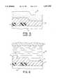
- FIG. 1shows a cross-section of a substrate S with a polyimide P layer. Two trenches are shown. The narrow trench on the left is bordered by two sections of the-polyimide P layer. A left-hand edge of a wide trench is shown on the right.
- Copperis damascene plated onto the patterned substrate S and polyimide P, blanketing both with a layer of copper metal. This is shown in FIG. 2, labelled “prior art,” where the copper is indicated by “Cu”.
- the copper layertends toward uniform thickness, but will bridge small openings in the polyimide P pattern, which tend to fill in as the plating accumulates.
- the POR (Plan of Record) commercial electroplating processexhibits this behavior.
- trenchesare narrow only a crease or cleft R is left in the upper surface of the copper plated layer, as shown in FIG. 2.
- Narrow polyimide gapsyield trenches with relatively small cleft depth. Since the surface becomes flatter as the copper thickness increases, it is said to be "planarized" by the copper fill-in.
- the copper layeris generally uniform in thickness, so it follows the original surface of the polyimide P layer, except for rounding of sharp corners.
- Planarization (planing) of the first metal layeris required for DLM.
- FIG. 3, labelled “prior art,”shows the copper layer of FIG. 2 after planarization.
- the copperis desirably removed from areas outside the trenches to form the lines.
- the next layer of linescan then be laid out in a pattern of cross-wiring on the flat surface. In FIG. 3 the second-level lines would lie parallel to the plane of the page.
- the layer's patternis contained in an image projected through a lens onto the substrate, which is coated with a light-sensitive material called photoresist.
- the lighthardens the photoresist that will form the trenches, while the unexposed photoresist is not cured and can be washed away. Due to built-in limitations of lenses, the image cannot be focussed onto a surface that is not perfectly flat.
- Micro-millingis one conventional planarization technique. Micro-milling is simply a miniaturized version of ordinary milling, employing a rotating milling cutter turned by a motor and mechanically scanned across a workpiece (here, the substrate) to level the surface.
- micro-milling method of planarizationhas several problems: alignment of parts to the plane of the milling cutter; induced stresses from the cutting operation that can cause cracking and delimitation; and contamination of the polyimide by smeared copper form the milling cutter.
- Micro-millingis also expensive. It involves a large capital cost and much labor. The yield (percentage of good parts emerging from the process) is low.
- Electrochemical machiningis an alternative to mechanical planarization.
- ECMis based on electrochemical etching, the dissolving of metals by a combination of salty water and electricity in a speeded-up, controlled sort of corrosion.
- ECMis safe, non-polluting, and often cheaper than mechanical machining. It can be used to machine very hard metals and cut cleanly through metal foils. It leaves no stress in the worked material and no deposits.
- FIG. 4illustrates the background art of electrochemical etching.
- the apparatus shownis a basic electroetching cell.
- a tank Tholds liquid electrolyte E, an aqueous solution of a salt.
- Two electrodes, the anode A and the cathode C,are wired to a voltage source such as a battery B.
- a voltage sourcesuch as a battery B.
- metal atoms in the anode Aare ionized by the electricity and forced out of the metal into the solution, and the metal anode A dissolves into the water.
- the rate of dissolutionis proportional to the electric current, according to Faraday's law.
- the metal ions from the cathodeeither plate the cathode, fall out as precipitate, or stay in solution.
- the cathodeis a shaped tool held close to the anode and slowly moved toward it while electrolyte is pumped through the inter-electrode gap.
- the anodeis the workpiece, and the cathode corresponds to the cutter of a mechanical machine tool which is slowly moved toward the work; the workpiece assumes the shape of the cathode as the operation progresses. There is no wear on the cathode, as the electrodes never touch.
- ECMcan be used to make complex pieces like gears.
- ECM metalis removed simply by bringing the cathode progressively nearer the work piece.
- the highest dissolution rates on the anodeare in places where the cathode has closely approached the anode surface, and the rate falls off as the inter-electrode distance increases. This is because of electrical field effects. Because of these effects the shape taken on by the anode is not exactly the shape of the cathode, and ECM tool designers must solve the Laplace equation, or use experimental methods involving electrically resistive paper, in order to get the proper cathode shape. See Electrochemical Machining, A. E. De Barr and D. A. Oliver ed., at pp. 155 et seq. (American Elsevier, New York, 1986).
- Electrolyte flow between the cathode and the workpieceis fast in conventional ECM, to speed etching and carry away heat. Pumping can be a problem due to the close spacing and high flow rates. Viscous liquids are not desirable for ECM electrolyte because they aggravate the pumping problem.
- ECMelectrochemical micromachining
- electropolished surfacescan be achieved in ECM and EMM.
- electropolishingcreates a very smooth mirror-like surface, said to be specular or bright, whose roughness is smaller than a wavelength of light.
- an electropolished surfacehas no built-up stress left by the high pressures of machining and mechanical polishing.
- the concentration of metal ions at the anode surfaceis significantly different from that of the bulk. Since these concentrations are mainly determined by the rate of mass transport, transport mechanisms and diffusion layer thickness play an important role in high rate anodic dissolution (see M. Datta, IBM Journal of Research and Development, no. 37, p 207, 1993).
- the Nernst diffusion layer conceptis used to obtain a simplified description of Mass transport effects in high-rate anodic dissolution of metals. According to this concept, a stagnant diffusion layer is assumed to exist at the anode. The dissolved metal ions that are produced at the anode are transported into the bulk electrolyte by convective diffusion. This leads to a concentration gradient inside the diffusion layer.
- the thickness of the diffusion layerdepends on the hydrodynamic conditions, i.e. the degree of electrolyte agitation and physical properties of the electrolyte such as its viscosity. Under ECM conditions the diffusion layer thickness may vary between 10 and 50 microns. The diffusion layer, thus, tends to bridge the narrow gaps but follow the contours of wider features.
- FIG. 5shows a diffusion layer D bridging the cleft R but following the contours of the wide trench on the right side of FIG. 2. Planarization of wide features does not occur under mass transport/electropolishing conditions.
- Viscosity of the electrolyteis a factor in the amount of Brownian motion, so diffusion is slowed down by adding to the electrolyte substances that increase the viscosity of the electrolyte. Increasing the electrolyte viscosity thickens the diffusion layer and promotes surface polishing. (See A. E. De Barr and D. A. Oliver at page 102.)
- the diffusion layercould perhaps be thickened to the point where it would bridge wider features, but this would require making the electrolyte extremely viscous. Extremely high viscosity would slow the rate of metal removal and prevent the electrolyte from being pumped through the electrolytic cell at adequate speeds.
- aqueous electrolytewith a viscous liquid generally results in a more viscous electrolyte, as would be expected.
- Glycerinewhich has a viscosity at room temperature about 1500 times that of water, is used in electroetching to increase the electrolyte viscosity and promote polishing.
- the viscosity of a mixture of two liquidsis not the average of their viscosities, in general.
- the electrical resistivity of an aqueous electrolytecan also be increased by adding certain substances.
- Resistivityor specific resistivity, is a property of the electrolyte substance and not of the cell geometry. Its relation to the electrical resistance of the cell is like that of density to mass.
- Resistance additivesare not the same as viscosity additives, however; a substance which increases viscosity may not increase resistance at all, or may increase it very much.
- Taylors' attempts to find a relation between the viscosity of electrolytes their resistivityhave been unsuccessful. Viscosity and resistivity appear to be independent.
- an additive substancemay increase the viscosity without increasing the resistance of an electrolyte, or conversely.
- Electrolyte resistivityhas an effect on electroetching, but the effect is of a different sort from that caused by viscosity.
- the viscosityaffects diffusion in the region very close to the metal surface to alter the so-called tertiary current distribution in the electrolytic cell.
- the primary current distributionis related to Ohm's law and is a function of the electrolyte resistivity, any internal resistance of electrodes, and the cell geometry.
- E. Der Matosianin U.S. Pat. No. 2,516,105, teaches electrolytic polishing of metals. He discloses the use of organic solvents as part of the electrolyte solution (at col. 2, line 26), and mentions various substances, including ethylene glycol (end of col. 2). The function of the glycol is given as concentration polarization at the anode.
- Milton J. Riddles and Josephine Williamsin U.S. Pat. No. 3,334,210, disclose an electrolyte formula based on polyethylene glycols in an aqueous solution.
- the solutionsare employed in arc machining with high-frequency electrical discharges.
- an electrochemical cellcomprises a second electrode generally parallel to the first electrode surface; an aqueous electrolyte disposed between the second electrode and the first electrode surface; an electrical resistance additive substance mixed with the electrolyte to form a resistive electrolytic mixture; and a source of voltage.
- a potential differenceis placed across the cell by the source of voltage, the first electrode surface is electrochemically planarized.
- FIG. 1, labelled “prior art,”is a cross-sectional view of a substrate and polyimide layer.
- FIG. 2is cross-sectional view of the substrate of FIG. 1 with damascened copper filling narrow and wide trenches in the polyimide layer.
- FIG. 3shows the copper layer of FIG. 2 after planarization.
- FIG. 4, labelled “prior art,”is a schematic view of an electropolishing apparatus.
- FIG. 5, labelled “prior art,”shows a diffusion layer formed over the copper layer of FIG. 2 during electroetching.
- FIG. 6is a schematic view of the present invention applied to the copper layer of FIG. 2.
- FIG. 7is a perspective view of a multi-nozzle assembly for linear jet etching.
- the present inventionrelates to an electrochemical micro-machining (EMM) process and apparatus for planarizing (planing or making flat) uneven metal surfaces. It is especially useful for fabricating DLM structures for microelectronic circuits.
- ECMelectrochemical micro-machining
- the inventionemploys an electrolyte made electrically resistive through the addition of a non-conducting organic substance, such as ethylene glycol.
- a non-conducting organic substancesuch as ethylene glycol.
- the inventionalso uses a short inter-electrode distance between the etched surface and the cathode.
- a linear multi-nozzle electrode assemblywhich localizes both electrolyte flow and current along a small area of the sample is preferably used for etching.
- the multi-nozzle electrodeis slowly scanned back and forth over the substrate. Concentration of etching in a small area allows high current density for electropolishing without the need for a large total current, reduces stray currents, improves electrolyte flow, and allows simpler and less expensive mechanical fabrication.
- electrolytewhen applied to an aqueous solution--a solution with both water and solute, and not just the solute;
- FIG. 6An electrolytic cell is shown in FIG. 6.
- the copper Cu layeris labelled A for anode.
- the layer Ahas a cleft R, a lower surface L over a wide trench, and an upper surface U over the polyimide P layer.
- Disposed above the anode Ais a cathode C, which has a plane or straight surface aligned parallel to the substrate S, which is flat.
- An electrolyte Efills the space between the anode A and cathode C.
- the cathode C and the anode Aare connected to the negative and positive poles, respectively, of a power supply or other conventional device which can establish a voltage between them (not shown).
- the anode A and cathode Cbeing of metal, have essentially constant respective voltages throughout.
- the facing parallel surfacesare each at a respective equipotential.
- the applied voltage from the voltage source Bcauses an electric current to flow in the electrolyte E between the anode A and cathode C.
- the amount of currentis given by Ohm's law,
- Icurrent in amperes
- Ethe potential difference between the electrodes in volts
- Rthe resistance of the electrolyte in ohms.
- the resistance R of the electrolyte between the anode A and cathode Cis a function of the cell geometry and the electrolyte resistivity. If in FIG. 6 the electrolyte is drained and replaced with electrolyte of higher resistivity but the distance between the anode A and cathode C is kept constant, then the cell resistance will be increased in the same proportion as the resistivity. The resistance may be constant if the electrolyte resistivity is increased but at the same time the inter-electrode distance is decreased.
- each electrode surfaceis an equipotential line (line of constant voltage); within the electrolyte, lines of constant voltage are generally horizontal and parallel to the electrode surfaces.
- a more-resistive electrolytewill cause a greater voltage drop between the electrodes; there will be more equipotential lines in the inter-electrode space.
- the more crowded linesmean a greater voltage gradient, which will accelerate the planing action caused by bending of the equipotential lines near protrusions from the anode A surface.
- a first aspect of the inventioninvolves the use of an electrolyte with increased resistivity.
- the resistivity of a salt/water electrolyteis of the order of a few ohms across a cubic centimeter of electrolyte. It varies with the salt and the temperature, but the main factor in resistivity is the concentration of the solution. To increase resistivity, the salt concentration can be lowered. However, to provide enough water ions for fast etching, the salt concentration should be high. In the present invention, it is desired to increase the electrolyte resistivity but not to decrease the number of ions.
- the present inventionemploys non-conducting additives to the aqueous electrolyte of the cell.
- the preferred additiveis 2 M ethylene glycol.
- Mis molarity
- Ethylene glycoldoes not have an extremely large viscosity, as glycerine does. Glycol's viscosity is about 20 centipoises at room temperature, as compared to 1.0 centipoise for water and 1500 for glycerine.
- the inventioncontemplates maintaining electrolyte within a specified temperature range.
- the preferred electrolyteis 3 M NaNO 3 (sodium nitrate) in water.
- NaNO 3sodium nitrate
- metal dissolutionis not accompanied by oxygen evolution.
- Sodium nitrateis therefore preferable to phosphoric acid where oxygen evolution causes pitting on the copper anode A surface.
- NaClsodium chloride
- Electropolishingtakes place above the limiting current. Current rises with voltage at first, then levels off. The plateau current is the "limiting" current, even though the current can rise higher if enough voltage is applied.
- Anodic polarization of copper in nitrateis qualitatively the same as in phosphoric acid (used in the LLNL device) but the limiting current in phosphoric acid is much lower than in sodium nitrate solution, because in phosphoric acid oxygen evolution takes place below the limiting current. Oxygen evolution under extreme conditions leads to pits and cavities. In nitrate, on the other hand, the dissolution valence of copper is lower than 2 at current densities higher than the limiting current plateau. Because there is no oxygen evolution, no pitting or cavitation is present with the nitrate solution.
- the use of non-conducting additives to increase electrolyte resistivitydepends in part upon the cell geometry.
- the cathode C surfaceis desirably parallel to the anode A surface, so that the average inter-electrode distance is constant over the whole substrate S.
- the inter-electrode distancevaries locally, since the anode A is rough and in need of planarizing. If the cathode C is cocked, then the resistance across the anode A will vary and so will the current density, the etching rate, and the degree of planarization.
- the cathode C surfaceshould be parallel to the average level of the anode A surface.
- Another aspect of the inventionis short inter-electrode spacing, on the order of millimeters.
- the inter- electrode spacing between the upper surface U and the cathode Cis comparable to that between the upper surface U and the cathode C.
- the absolute elevation difference between the surfaces U and Ldoes change if the cathode C is moved farther away, but the proportional difference between the inter-electrode distances C-U and C-L is decreased.
- the cell of FIG. 6is divided down the middle, so that there are two independent cells having different respective inter-electrode spacings, the cell with the lesser spacing has lower resistance, because the electrolyte distance traversed by the current is shorter. If the spacing of both cells is increased by the same amount, the percentage difference in cell resistances decreases as both resistances' absolute values is increased. Therefore, the difference in etching rate decreases too if the same voltage is applied across both. That is, increases as the inter-electrode spacings decrease.
- the two sidesact somewhat as would two independent cells. This is because current tends to go straight across from anode to cathode. In a broad flat area, whether high or low, the lines of equipotential are generally flat. Current flows directly across the equipotential lines; current parallel to the electrode surfaces is minimal. At corners and edges of the anode A surface the equipotential lines bend, and the current has a horizontal component. In smoothing a rough anode surface, the etching rate differential again increases as the inter-electrode spacing decreases.
- the proportional etching rate difference between high and low areas of the anode Aresults in planarization.
- the absolute etch rateis irrelevant to planarization, but a high absolute rate is desirable for fast production.
- the second aspect of the inventionaugments the first aspect.
- a highly-resistive electrolytedoes not increase the percentage difference in current due to decreasing the inter- electrode gap; but resistive electrolyte increases the total current and so increase the absolute current difference for a given proportional difference.
- resistive electrolyteincreases the total current and so increase the absolute current difference for a given proportional difference.
- the cathode C and anode Aare desirably parallel.
- the cathode C surfaceis desirably relatively smooth as compared to the anode A surface. If the cathode C surface is rough planarization may not occur; instead, the anode surface may take on the contours of the cathode instead of being smoothed, as in large-scale conventional ECM.
- the rate differential and the thickness of the plated copper layer of the anode Acan be adjusted to allow the surface to be planarized as shown in FIG. 3.
- a third aspect of the present inventionis the use of a linear electrode which is scanned slowly back and forth over the anode, parallel to the substrate surface.
- FIG. 7shows the preferred embodiment of a linear electrode.
- This apparatusis substantially the same as that disclosed in U.S. Pat. No. 5,284,554, issued to Datta et al. on Feb. 8, 1994, assigned to International Business Machines Corporation, and incorporated herein by reference.
- the drawing numbersare equal to the drawing numbers of the '554 patent plus 100, for the corresponding parts.
- a nozzle assembly 126is shown in position below a substrate holder 124.
- the substrate holder 124is fixed to a moving stage 112 which moves axially by a conventional mechanism (not shown) to slowly sweep the carrier stage 112 over the nozzle assembly 126 as indicated by the arrow in FIG. 7.
- the scan speedis adjustable.
- a nozzle plate 128is mounted atop the hollow elongated nozzle assembly 126, which is made of plexiglass or the like.
- the nozzle plate 128contains many through holes 129.
- the interior space contained by the walls of the nozzle assembly 126 and the nozzle plate 128is filled with pressurized electrolyte (not shown) through a fitting 130.
- the electrolytespurts out through the plurality of holes 129, creating an elongated jet of electrolyte atop the nozzle plate 128, which is about 2 cm wide and about 15 cm long.
- the holesare carefully spaced on 3 -mm centers, and the diameter of the holes is 2 mm.
- the substrate Sis removably attached to the underside of the substrate holder 124 in an inverted position, and is not visible in FIG. 7.
- the clearance between the top surface of the nozzle plate 128 and the anode A layer, as the stage 112 scans the holder 124 over the nozzle assembly 126,is 3 -mm.
- electrolytecompletely fills the 3 mm inter-electrode gap and then runs down over the nozzle assembly 126. Etching takes place only where the electrolyte impinges, over the nozzle plate 128.
- the preferred flow rateis 1.5 gallons per minute with 3 M NaNO 3 and 2 M ethylene glycol as the electrolyte.
- the preferred scan rateis 2 cm/s.
- Nozzle plate 128is desirably comprised of stainless steel. It includes a tab 127 for electrical connection to a power supply (not shown). The plate 128 serves as a cathode. The opposite-polarity terminal of the power supply is connected to the plated copper layer (A in FIG. 6; not visible in FIG. 7.)
- Voltagecan be applied either as a steady DC (direct current) or as PC (pulsating current).
- a voltage of 10 Vis delivered in pulses lasting 10 ms (ms is the symbol for a millisecond, a thousandth of a second).
- the duty cycle(proportion of time during which the electricity is applied) is 30%.
- the metal removal rateis 1.4 micron/min.
- a layer of metal 8.3 microns thickwas removed and the surface examined. It was found that the difference between the highest and lowest points on the surface (the peak-to-peak variation) was 1 micron, or 12% of the total of 8.3 ⁇ . The average variation over the surface was 3.5%.
- the present inventionis simpler, removes metal faster, is safer, and creates less hazardous waste than the LLNL device.
- the thin linear electrodehas a surface area less than the area of the anodic copper layer in most cases. Because of this, its use reduces the amount of total current required for the electroetching device while keeping the local current density high. A large current density is needed for electropolishing, but a large total current requires larger and more expensive electrical components: wires, transformers, diodes, and switching circuits used for pulsed current.
- the multi-nozzle cellcan be used for plating as well as for etching, by reversing the voltage polarity and changing the electrolyte.
- the substrate Smay thus be plated and then etched without removing it from the holder 124.
- Many of the advantages and aspects of the present invention for etchingwill carry over to plating, which is a process converse to etching.
- the inventioncan be applied to the fabrication of thin-film packages.
- the processmay also find application in many other electronic packages and components where excess layers of conducting materials are required to be removed without introducing defects.
- the invention's techniquemay be used instead of chemical-mechanical polishing (eg., to remove excess copper in BEOL).
- the inventioncan also be applied to curved anode surfaces as well as to flat ones, for example, a cylindrical or conical surface over which a straight linear electrode can scan.
- Doubly-curved anode surfacessuch as hemispheres, can be scanned by a curved linear electrode.
- planeshall be interpreted to mean smoothing, i.e., making locally plane.
- metalmay be removed at a high rate of speed (e.g. 1.4 micron/min).
- a neutral salt solutione.g. Sodium Nitrate
- safety and waste disposal problemsare minimized.
- the simplified toolcan be readily manufactured and maintained.
Landscapes
- Chemical & Material Sciences (AREA)
- Engineering & Computer Science (AREA)
- Chemical Kinetics & Catalysis (AREA)
- Electrochemistry (AREA)
- Materials Engineering (AREA)
- Metallurgy (AREA)
- Organic Chemistry (AREA)
- Mechanical Engineering (AREA)
- Electrodes Of Semiconductors (AREA)
- Electrical Discharge Machining, Electrochemical Machining, And Combined Machining (AREA)
Abstract
Description
Claims (22)
Priority Applications (3)
| Application Number | Priority Date | Filing Date | Title |
|---|---|---|---|
| US08/300,623US5567300A (en) | 1994-09-02 | 1994-09-02 | Electrochemical metal removal technique for planarization of surfaces |
| EP95111329AEP0699782A1 (en) | 1994-09-02 | 1995-07-19 | High speed electrochemical metal removal technique for planarization of DLM structure using neutral salt electrolytes |
| JP22486095AJP3245017B2 (en) | 1994-09-02 | 1995-09-01 | High-speed electrochemical electrolytic cell for flattening DLM structure |
Applications Claiming Priority (1)
| Application Number | Priority Date | Filing Date | Title |
|---|---|---|---|
| US08/300,623US5567300A (en) | 1994-09-02 | 1994-09-02 | Electrochemical metal removal technique for planarization of surfaces |
Publications (1)
| Publication Number | Publication Date |
|---|---|
| US5567300Atrue US5567300A (en) | 1996-10-22 |
Family
ID=23159890
Family Applications (1)
| Application Number | Title | Priority Date | Filing Date |
|---|---|---|---|
| US08/300,623Expired - LifetimeUS5567300A (en) | 1994-09-02 | 1994-09-02 | Electrochemical metal removal technique for planarization of surfaces |
Country Status (3)
| Country | Link |
|---|---|
| US (1) | US5567300A (en) |
| EP (1) | EP0699782A1 (en) |
| JP (1) | JP3245017B2 (en) |
Cited By (188)
| Publication number | Priority date | Publication date | Assignee | Title |
|---|---|---|---|---|
| US5807165A (en)* | 1997-03-26 | 1998-09-15 | International Business Machines Corporation | Method of electrochemical mechanical planarization |
| US5865984A (en)* | 1997-06-30 | 1999-02-02 | International Business Machines Corporation | Electrochemical etching apparatus and method for spirally etching a workpiece |
| US5911619A (en)* | 1997-03-26 | 1999-06-15 | International Business Machines Corporation | Apparatus for electrochemical mechanical planarization |
| WO1999065072A1 (en)* | 1998-06-11 | 1999-12-16 | Speedfam-Ipec Corporation | Electrochemical planarization of metal layers using a bipolar electrode assembly |
| US6056869A (en)* | 1998-06-04 | 2000-05-02 | International Business Machines Corporation | Wafer edge deplater for chemical mechanical polishing of substrates |
| US6071388A (en)* | 1998-05-29 | 2000-06-06 | International Business Machines Corporation | Electroplating workpiece fixture having liquid gap spacer |
| US6132586A (en)* | 1998-06-11 | 2000-10-17 | Integrated Process Equipment Corporation | Method and apparatus for non-contact metal plating of semiconductor wafers using a bipolar electrode assembly |
| US6143155A (en)* | 1998-06-11 | 2000-11-07 | Speedfam Ipec Corp. | Method for simultaneous non-contact electrochemical plating and planarizing of semiconductor wafers using a bipiolar electrode assembly |
| US6150269A (en)* | 1998-09-11 | 2000-11-21 | Chartered Semiconductor Manufacturing Company, Ltd. | Copper interconnect patterning |
| US6149830A (en)* | 1998-09-17 | 2000-11-21 | Siemens Aktiengesellschaft | Composition and method for reducing dishing in patterned metal during CMP process |
| US6228231B1 (en) | 1997-05-29 | 2001-05-08 | International Business Machines Corporation | Electroplating workpiece fixture having liquid gap spacer |
| US6242343B1 (en)* | 1996-02-05 | 2001-06-05 | Semiconductor Energy Laboratory Co., Ltd. | Process for fabricating semiconductor device and apparatus for fabricating semiconductor device |
| US6303506B1 (en) | 1999-09-30 | 2001-10-16 | Infineon Technologies Ag | Compositions for and method of reducing/eliminating scratches and defects in silicon dioxide during CMP process |
| US20020000613A1 (en)* | 1997-11-27 | 2002-01-03 | Hisashi Ohtani | Semiconductor device |
| US20020033341A1 (en)* | 1998-10-14 | 2002-03-21 | Taylor E. Jennings | Pulse reverse electrodeposition for metallization and planarization of semiconductor substrates |
| US6395152B1 (en) | 1998-07-09 | 2002-05-28 | Acm Research, Inc. | Methods and apparatus for electropolishing metal interconnections on semiconductor devices |
| US6398941B2 (en)* | 1997-06-13 | 2002-06-04 | General Electric Company | Method of shaping a workpiece using an electrochemical machining tool |
| US6447668B1 (en) | 1998-07-09 | 2002-09-10 | Acm Research, Inc. | Methods and apparatus for end-point detection |
| US20020130034A1 (en)* | 2000-02-23 | 2002-09-19 | Nutool Inc. | Pad designs and structures for a versatile materials processing apparatus |
| US6455415B1 (en)* | 1999-04-21 | 2002-09-24 | Advanced Micro Devices, Inc. | Method of encapsulated copper (Cu) interconnect formation |
| US6464855B1 (en) | 2000-10-04 | 2002-10-15 | Speedfam-Ipec Corporation | Method and apparatus for electrochemical planarization of a workpiece |
| US6495443B1 (en) | 2001-06-05 | 2002-12-17 | Advanced Micro Devices, Inc. | Method of re-working copper damascene wafers |
| US6524461B2 (en)* | 1998-10-14 | 2003-02-25 | Faraday Technology Marketing Group, Llc | Electrodeposition of metals in small recesses using modulated electric fields |
| US6534327B2 (en) | 2000-04-13 | 2003-03-18 | Texas Instruments Incorporated | Method for reworking metal layers on integrated circuit bond pads |
| US20030054729A1 (en)* | 2000-08-30 | 2003-03-20 | Whonchee Lee | Methods and apparatus for electromechanically and/or electrochemically-mechanically removing conductive material from a microelectronic substrate |
| US6537144B1 (en) | 2000-02-17 | 2003-03-25 | Applied Materials, Inc. | Method and apparatus for enhanced CMP using metals having reductive properties |
| US20030057097A1 (en)* | 2001-09-21 | 2003-03-27 | Applied Materials, Inc. | Method and apparatus for forming metal layers |
| US20030066760A1 (en)* | 2001-10-03 | 2003-04-10 | Yoshitaka Matsui | Electropolishing method |
| US6547167B1 (en)* | 1999-01-26 | 2003-04-15 | Jeffrey Fugere | Fluid dispense tips |
| US20030072639A1 (en)* | 2001-10-17 | 2003-04-17 | Applied Materials, Inc. | Substrate support |
| US20030070930A1 (en)* | 2000-03-17 | 2003-04-17 | Homayoun Talieh | Device providing electrical contact to the surface of a semiconductor workpiece during metal plating and method of providing such contact |
| WO2003042433A1 (en)* | 2001-11-13 | 2003-05-22 | Acm Research, Inc. | Electropolishing assembly and methods for electropolishing conductive layers |
| US20030094364A1 (en)* | 1998-12-01 | 2003-05-22 | Homayoun Talieh | Method and apparatus for electro-chemical mechanical deposition |
| US6592742B2 (en) | 2001-07-13 | 2003-07-15 | Applied Materials Inc. | Electrochemically assisted chemical polish |
| US6596150B2 (en)* | 1998-05-28 | 2003-07-22 | Fuji Photo Film Co., Ltd. | Production method for an aluminum support for a lithographic printing plate |
| US6599415B1 (en)* | 2001-04-30 | 2003-07-29 | Advanced Cardiovascular Systems, Inc. | Apparatus and method for electropolishing surfaces |
| US20030146089A1 (en)* | 2000-08-10 | 2003-08-07 | Bulent Basol | Plating method and apparatus that creates a differential between additive disposed on a top surface and a cavity surface of a workpiece using an external influence |
| US20030155255A1 (en)* | 2002-01-22 | 2003-08-21 | Applied Materials, Inc. | Electropolishing of metallic interconnects |
| US6613200B2 (en) | 2001-01-26 | 2003-09-02 | Applied Materials, Inc. | Electro-chemical plating with reduced thickness and integration with chemical mechanical polisher into a single platform |
| US20030205484A1 (en)* | 2002-05-02 | 2003-11-06 | Madhav Datta | Electrochemical/ mechanical polishing |
| US20030209523A1 (en)* | 2002-05-09 | 2003-11-13 | Applied Materials, Inc. | Planarization by chemical polishing for ULSI applications |
| US6649513B1 (en) | 2002-05-15 | 2003-11-18 | Taiwan Semiconductor Manufacturing Company | Copper back-end-of-line by electropolish |
| US20030213703A1 (en)* | 2002-05-16 | 2003-11-20 | Applied Materials, Inc. | Method and apparatus for substrate polishing |
| US20030221953A1 (en)* | 2000-01-03 | 2003-12-04 | Oberlitner Thomas H. | Microelectronic workpiece processing tool including a processing reactor having a paddle assembly for agitation of a processing fluid proximate to the workpiece |
| US20030234184A1 (en)* | 2001-03-14 | 2003-12-25 | Applied Materials, Inc. | Method and composition for polishing a substrate |
| US20040043582A1 (en)* | 2002-08-29 | 2004-03-04 | Dinesh Chopra | Method and apparatus for simultaneously removing multiple conductive materials from microelectronic substrates |
| US20040043629A1 (en)* | 2002-08-29 | 2004-03-04 | Whonchee Lee | Method and apparatus for removing adjacent conductive and nonconductive materials of a microelectronic substrate |
| US20040053512A1 (en)* | 2002-09-16 | 2004-03-18 | Applied Materials, Inc. | Process control in electrochemically assisted planarization |
| US20040053560A1 (en)* | 2002-09-16 | 2004-03-18 | Lizhong Sun | Control of removal profile in electrochemically assisted CMP |
| US20040053499A1 (en)* | 2001-03-14 | 2004-03-18 | Applied Materials, Inc. | Method and composition for polishing a substrate |
| US6719615B1 (en) | 2000-10-10 | 2004-04-13 | Beaver Creek Concepts Inc | Versatile wafer refining |
| EP1104013A3 (en)* | 1999-11-29 | 2004-04-14 | Applied Materials, Inc. | Advanced electrolytic polish assisted metal wafer planarization |
| US6736952B2 (en) | 2001-02-12 | 2004-05-18 | Speedfam-Ipec Corporation | Method and apparatus for electrochemical planarization of a workpiece |
| US20040097070A1 (en)* | 2002-01-07 | 2004-05-20 | Shuzo Sato | Method of producing metal film |
| US20040125384A1 (en)* | 1998-07-09 | 2004-07-01 | Hui Wang | Method and apparatus for end-point detection |
| US20040134793A1 (en)* | 2000-01-14 | 2004-07-15 | Uzoh Cyprian Emeka | Workpiece proximity etching method and apparatus |
| US20040170753A1 (en)* | 2000-12-18 | 2004-09-02 | Basol Bulent M. | Electrochemical mechanical processing using low temperature process environment |
| US20040173461A1 (en)* | 2003-03-04 | 2004-09-09 | Applied Materials, Inc. | Method and apparatus for local polishing control |
| US20040182721A1 (en)* | 2003-03-18 | 2004-09-23 | Applied Materials, Inc. | Process control in electro-chemical mechanical polishing |
| US6796887B2 (en) | 2002-11-13 | 2004-09-28 | Speedfam-Ipec Corporation | Wear ring assembly |
| US20040200728A1 (en)* | 2000-06-29 | 2004-10-14 | Akihisa Hongo | Method and apparatus for forming interconnects, and polishing liquid and polishing method |
| US6811680B2 (en) | 2001-03-14 | 2004-11-02 | Applied Materials Inc. | Planarization of substrates using electrochemical mechanical polishing |
| US6815336B1 (en)* | 1998-09-25 | 2004-11-09 | Taiwan Semiconductor Manufacturing Company, Ltd. | Planarization of copper damascene using reverse current electroplating and chemical mechanical polishing |
| US6821407B1 (en) | 2000-05-10 | 2004-11-23 | Novellus Systems, Inc. | Anode and anode chamber for copper electroplating |
| US20040235297A1 (en)* | 2003-05-23 | 2004-11-25 | Bih-Tiao Lin | Reverse electroplating for damascene conductive region formation |
| US20040245094A1 (en)* | 2003-06-06 | 2004-12-09 | Mchugh Paul R. | Integrated microfeature workpiece processing tools with registration systems for paddle reactors |
| US20040262168A1 (en)* | 2003-06-25 | 2004-12-30 | Jinshan Huo | Methods of electopolishing patterned substrates |
| US6837983B2 (en) | 2002-01-22 | 2005-01-04 | Applied Materials, Inc. | Endpoint detection for electro chemical mechanical polishing and electropolishing processes |
| US20050000817A1 (en)* | 2003-07-01 | 2005-01-06 | Mchugh Paul R. | Reactors having multiple electrodes and/or enclosed reciprocating paddles, and associated methods |
| US20050020192A1 (en)* | 2002-08-29 | 2005-01-27 | Whonchee Lee | Method and apparatus for chemically, mechanically, and/or electrolytically removing material from microelectronic substrates |
| US6856360B1 (en) | 1997-11-28 | 2005-02-15 | Semiconductor Energy Laboratory Co., Ltd. | Electrooptical device, method of manufacturing the same, and electronic equipment |
| US20050034977A1 (en)* | 2003-06-06 | 2005-02-17 | Hanson Kyle M. | Electrochemical deposition chambers for depositing materials onto microfeature workpieces |
| US6863797B2 (en) | 2001-12-21 | 2005-03-08 | Applied Materials, Inc. | Electrolyte with good planarization capability, high removal rate and smooth surface finish for electrochemically controlled copper CMP |
| US20050050767A1 (en)* | 2003-06-06 | 2005-03-10 | Hanson Kyle M. | Wet chemical processing chambers for processing microfeature workpieces |
| US6867448B1 (en) | 2000-08-31 | 2005-03-15 | Micron Technology, Inc. | Electro-mechanically polished structure |
| US20050059324A1 (en)* | 2003-09-17 | 2005-03-17 | Whonchee Lee | Methods and apparatus for removing conductive material from a microelectronic substrate |
| US20050063798A1 (en)* | 2003-06-06 | 2005-03-24 | Davis Jeffry Alan | Interchangeable workpiece handling apparatus and associated tool for processing microfeature workpieces |
| US20050061674A1 (en)* | 2002-09-16 | 2005-03-24 | Yan Wang | Endpoint compensation in electroprocessing |
| US6890416B1 (en) | 2000-05-10 | 2005-05-10 | Novellus Systems, Inc. | Copper electroplating method and apparatus |
| US20050100457A1 (en)* | 2000-01-26 | 2005-05-12 | Dl Technology, Llc | System and method for control of fluid dispense pump |
| US6896776B2 (en) | 2000-12-18 | 2005-05-24 | Applied Materials Inc. | Method and apparatus for electro-chemical processing |
| US20050112868A1 (en)* | 2003-11-21 | 2005-05-26 | Basol Bulent M. | Method and apparatus for localized material removal by electrochemical polishing |
| US20050124262A1 (en)* | 2003-12-03 | 2005-06-09 | Applied Materials, Inc. | Processing pad assembly with zone control |
| US20050139897A1 (en)* | 2003-12-31 | 2005-06-30 | Dongbuanam Semiconductor Inc. | Non-volatile flash memory device |
| US20050145506A1 (en)* | 2003-12-29 | 2005-07-07 | Taylor E. J. | Electrochemical etching of circuitry for high density interconnect electronic modules |
| US6919010B1 (en) | 2001-06-28 | 2005-07-19 | Novellus Systems, Inc. | Uniform electroplating of thin metal seeded wafers using rotationally asymmetric variable anode correction |
| US20050196963A1 (en)* | 2004-02-20 | 2005-09-08 | Whonchee Lee | Methods and apparatuses for electrochemical-mechanical polishing |
| US20050224358A1 (en)* | 2004-03-30 | 2005-10-13 | Lsi Logic Corporation | Method for improved local planarity control during electropolishing |
| US6957783B1 (en) | 1999-01-26 | 2005-10-25 | Dl Technology Llc | Dispense tip with vented outlets |
| US6962524B2 (en) | 2000-02-17 | 2005-11-08 | Applied Materials, Inc. | Conductive polishing article for electrochemical mechanical polishing |
| US6979248B2 (en) | 2002-05-07 | 2005-12-27 | Applied Materials, Inc. | Conductive polishing article for electrochemical mechanical polishing |
| US6981664B1 (en)* | 2000-01-26 | 2006-01-03 | Dl Technology Llc | Fluid dispense tips |
| US6983867B1 (en) | 2002-04-29 | 2006-01-10 | Dl Technology Llc | Fluid dispense pump with drip prevention mechanism and method for controlling same |
| US20060006060A1 (en)* | 2000-11-03 | 2006-01-12 | Basol Bulent M | Method and apparatus for processing a substrate with minimal edge exclusion |
| US6988942B2 (en) | 2000-02-17 | 2006-01-24 | Applied Materials Inc. | Conductive polishing article for electrochemical mechanical polishing |
| US7014538B2 (en) | 1999-05-03 | 2006-03-21 | Applied Materials, Inc. | Article for polishing semiconductor substrates |
| US7029365B2 (en) | 2000-02-17 | 2006-04-18 | Applied Materials Inc. | Pad assembly for electrochemical mechanical processing |
| US20060088872A1 (en)* | 2003-04-24 | 2006-04-27 | Afshin Ahmadian | Allele-specific mutation detection assay |
| US7059948B2 (en) | 2000-12-22 | 2006-06-13 | Applied Materials | Articles for polishing semiconductor substrates |
| US7074113B1 (en) | 2000-08-30 | 2006-07-11 | Micron Technology, Inc. | Methods and apparatus for removing conductive material from a microelectronic substrate |
| US7077721B2 (en) | 2000-02-17 | 2006-07-18 | Applied Materials, Inc. | Pad assembly for electrochemical mechanical processing |
| US20060163074A1 (en)* | 2002-09-16 | 2006-07-27 | Applied Materials, Inc. | Algorithm for real-time process control of electro-polishing |
| US20060166500A1 (en)* | 2005-01-26 | 2006-07-27 | Applied Materials, Inc. | Electroprocessing profile control |
| US7084064B2 (en) | 2004-09-14 | 2006-08-01 | Applied Materials, Inc. | Full sequence metal and barrier layer electrochemical mechanical processing |
| US20060183321A1 (en)* | 2004-09-27 | 2006-08-17 | Basol Bulent M | Method for reduction of gap fill defects |
| US7094131B2 (en)* | 2000-08-30 | 2006-08-22 | Micron Technology, Inc. | Microelectronic substrate having conductive material with blunt cornered apertures, and associated methods for removing conductive material |
| US20060207888A1 (en)* | 2003-12-29 | 2006-09-21 | Taylor E J | Electrochemical etching of circuitry for high density interconnect electronic modules |
| US7112121B2 (en) | 2000-08-30 | 2006-09-26 | Micron Technology, Inc. | Methods and apparatus for electrical, mechanical and/or chemical removal of conductive material from a microelectronic substrate |
| US7125477B2 (en) | 2000-02-17 | 2006-10-24 | Applied Materials, Inc. | Contacts for electrochemical processing |
| US7128825B2 (en) | 2001-03-14 | 2006-10-31 | Applied Materials, Inc. | Method and composition for polishing a substrate |
| US7134934B2 (en) | 2000-08-30 | 2006-11-14 | Micron Technology, Inc. | Methods and apparatus for electrically detecting characteristics of a microelectronic substrate and/or polishing medium |
| US7137879B2 (en) | 2001-04-24 | 2006-11-21 | Applied Materials, Inc. | Conductive polishing article for electrochemical mechanical polishing |
| US7153410B2 (en) | 2000-08-30 | 2006-12-26 | Micron Technology, Inc. | Methods and apparatus for electrochemical-mechanical processing of microelectronic workpieces |
| US7153195B2 (en) | 2000-08-30 | 2006-12-26 | Micron Technology, Inc. | Methods and apparatus for selectively removing conductive material from a microelectronic substrate |
| US7160176B2 (en) | 2000-08-30 | 2007-01-09 | Micron Technology, Inc. | Methods and apparatus for electrically and/or chemically-mechanically removing conductive material from a microelectronic substrate |
| US20070051635A1 (en)* | 2000-08-10 | 2007-03-08 | Basol Bulent M | Plating apparatus and method for controlling conductor deposition on predetermined portions of a wafer |
| US7207498B1 (en) | 2000-01-26 | 2007-04-24 | Dl Technology, Llc | Fluid dispense tips |
| US7207878B2 (en) | 2000-02-17 | 2007-04-24 | Applied Materials, Inc. | Conductive polishing article for electrochemical mechanical polishing |
| US20070117377A1 (en)* | 2005-11-23 | 2007-05-24 | Chih-Chao Yang | Conductor-dielectric structure and method for fabricating |
| US20070128851A1 (en)* | 2001-01-05 | 2007-06-07 | Novellus Systems, Inc. | Fabrication of semiconductor interconnect structures |
| KR100731107B1 (en) | 2005-12-29 | 2007-06-21 | 동부일렉트로닉스 주식회사 | Method for Forming Copper Metallization of Semiconductor Device Using Damascene Process |
| US20070144912A1 (en)* | 2003-07-01 | 2007-06-28 | Woodruff Daniel J | Linearly translating agitators for processing microfeature workpieces, and associated methods |
| US20070181443A1 (en)* | 2006-02-03 | 2007-08-09 | Basol Bulent M | Electrode and pad assembly for processing conductive layers |
| KR100780257B1 (en)* | 2000-09-19 | 2007-11-28 | 소니 가부시끼 가이샤 | Polishing method, polishing apparatus, plating method, and plating apparatus |
| US7303662B2 (en) | 2000-02-17 | 2007-12-04 | Applied Materials, Inc. | Contacts for electrochemical processing |
| US7303462B2 (en) | 2000-02-17 | 2007-12-04 | Applied Materials, Inc. | Edge bead removal by an electro polishing process |
| US7309407B2 (en) | 1999-03-30 | 2007-12-18 | Novellus Systems, Inc. | Method and apparatus for forming an electrical contact with a semiconductor substrate |
| US20080014709A1 (en)* | 2006-07-07 | 2008-01-17 | Applied Materials, Inc. | Method and apparatus for electroprocessing a substrate with edge profile control |
| US7323416B2 (en) | 2001-03-14 | 2008-01-29 | Applied Materials, Inc. | Method and composition for polishing a substrate |
| US7331482B1 (en) | 2003-03-28 | 2008-02-19 | Dl Technology, Llc | Dispense pump with heated pump housing and heated material reservoir |
| US20080057709A1 (en)* | 2006-08-30 | 2008-03-06 | Vladislav Vasilev | Method and apparatus for workpiece surface modification for selective material deposition |
| US7344432B2 (en) | 2001-04-24 | 2008-03-18 | Applied Materials, Inc. | Conductive pad with ion exchange membrane for electrochemical mechanical polishing |
| US7374644B2 (en) | 2000-02-17 | 2008-05-20 | Applied Materials, Inc. | Conductive polishing article for electrochemical mechanical polishing |
| US7377836B1 (en) | 2000-10-10 | 2008-05-27 | Beaver Creek Concepts Inc | Versatile wafer refining |
| US7390429B2 (en) | 2003-06-06 | 2008-06-24 | Applied Materials, Inc. | Method and composition for electrochemical mechanical polishing processing |
| US7390744B2 (en) | 2004-01-29 | 2008-06-24 | Applied Materials, Inc. | Method and composition for polishing a substrate |
| US20080178460A1 (en)* | 2007-01-29 | 2008-07-31 | Woodruff Daniel J | Protected magnets and magnet shielding for processing microfeature workpieces, and associated systems and methods |
| US20080181758A1 (en)* | 2007-01-29 | 2008-07-31 | Woodruff Daniel J | Microfeature workpiece transfer devices with rotational orientation sensors, and associated systems and methods |
| US7427340B2 (en) | 2005-04-08 | 2008-09-23 | Applied Materials, Inc. | Conductive pad |
| US7448857B1 (en) | 1999-11-08 | 2008-11-11 | Dl Technology, Llc | Fluid pump and cartridge |
| US7476304B2 (en) | 2000-03-17 | 2009-01-13 | Novellus Systems, Inc. | Apparatus for processing surface of workpiece with small electrodes and surface contacts |
| US7520968B2 (en) | 2004-10-05 | 2009-04-21 | Applied Materials, Inc. | Conductive pad design modification for better wafer-pad contact |
| US7566391B2 (en) | 2004-09-01 | 2009-07-28 | Micron Technology, Inc. | Methods and systems for removing materials from microfeature workpieces with organic and/or non-aqueous electrolytic media |
| US7582564B2 (en) | 2001-03-14 | 2009-09-01 | Applied Materials, Inc. | Process and composition for conductive material removal by electrochemical mechanical polishing |
| US7622024B1 (en) | 2000-05-10 | 2009-11-24 | Novellus Systems, Inc. | High resistance ionic current source |
| US7670468B2 (en) | 2000-02-17 | 2010-03-02 | Applied Materials, Inc. | Contact assembly and method for electrochemical mechanical processing |
| US20100062693A1 (en)* | 2008-09-05 | 2010-03-11 | Taiwan Semiconductor Manufacturing Co., Ltd. | Two step method and apparatus for polishing metal and other films in semiconductor manufacturing |
| US7678245B2 (en) | 2000-02-17 | 2010-03-16 | Applied Materials, Inc. | Method and apparatus for electrochemical mechanical processing |
| US7682498B1 (en) | 2001-06-28 | 2010-03-23 | Novellus Systems, Inc. | Rotationally asymmetric variable electrode correction |
| US20100116672A1 (en)* | 2008-11-07 | 2010-05-13 | Novellus Systems, Inc. | Method and apparatus for electroplating |
| US20100147679A1 (en)* | 2008-12-17 | 2010-06-17 | Novellus Systems, Inc. | Electroplating Apparatus with Vented Electrolyte Manifold |
| WO2010039491A3 (en)* | 2008-09-23 | 2010-07-01 | Kennametal Inc. | Electrolytic deburring apparatus and method |
| US7799684B1 (en)* | 2007-03-05 | 2010-09-21 | Novellus Systems, Inc. | Two step process for uniform across wafer deposition and void free filling on ruthenium coated wafers |
| US20100276522A1 (en)* | 2009-05-01 | 2010-11-04 | Dl Technology | Material dispense tips and methods for forming the same |
| US20110031115A1 (en)* | 2008-04-14 | 2011-02-10 | David Hillabrand | Manufacturing Apparatus For Depositing A Material On An Electrode For Use Therein |
| US20110036294A1 (en)* | 2008-04-14 | 2011-02-17 | David Hillabrand | Manufacturing Apparatus For Depositing A Material And An Electrode For Use Therein |
| US20110036292A1 (en)* | 2008-04-14 | 2011-02-17 | Max Dehtiar | Manufacturing Apparatus For Depositing A Material And An Electrode For Use Therein |
| US7947163B2 (en) | 2006-07-21 | 2011-05-24 | Novellus Systems, Inc. | Photoresist-free metal deposition |
| US7964506B1 (en) | 2008-03-06 | 2011-06-21 | Novellus Systems, Inc. | Two step copper electroplating process with anneal for uniform across wafer deposition and void free filling on ruthenium coated wafers |
| US8236160B2 (en) | 2000-08-10 | 2012-08-07 | Novellus Systems, Inc. | Plating methods for low aspect ratio cavities |
| US8262871B1 (en) | 2008-12-19 | 2012-09-11 | Novellus Systems, Inc. | Plating method and apparatus with multiple internally irrigated chambers |
| US8308931B2 (en) | 2006-08-16 | 2012-11-13 | Novellus Systems, Inc. | Method and apparatus for electroplating |
| US8513124B1 (en) | 2008-03-06 | 2013-08-20 | Novellus Systems, Inc. | Copper electroplating process for uniform across wafer deposition and void free filling on semi-noble metal coated wafers |
| US8575028B2 (en) | 2011-04-15 | 2013-11-05 | Novellus Systems, Inc. | Method and apparatus for filling interconnect structures |
| US8623193B1 (en) | 2004-06-16 | 2014-01-07 | Novellus Systems, Inc. | Method of electroplating using a high resistance ionic current source |
| US8703615B1 (en) | 2008-03-06 | 2014-04-22 | Novellus Systems, Inc. | Copper electroplating process for uniform across wafer deposition and void free filling on ruthenium coated wafers |
| US8707559B1 (en) | 2007-02-20 | 2014-04-29 | Dl Technology, Llc | Material dispense tips and methods for manufacturing the same |
| US8795480B2 (en) | 2010-07-02 | 2014-08-05 | Novellus Systems, Inc. | Control of electrolyte hydrodynamics for efficient mass transfer during electroplating |
| US20160053399A1 (en)* | 2014-08-25 | 2016-02-25 | Seiko Epson Corporation | Forming method and formed article |
| US9449808B2 (en) | 2013-05-29 | 2016-09-20 | Novellus Systems, Inc. | Apparatus for advanced packaging applications |
| US9523155B2 (en) | 2012-12-12 | 2016-12-20 | Novellus Systems, Inc. | Enhancement of electrolyte hydrodynamics for efficient mass transfer during electroplating |
| US9624592B2 (en) | 2010-07-02 | 2017-04-18 | Novellus Systems, Inc. | Cross flow manifold for electroplating apparatus |
| US9670588B2 (en) | 2013-05-01 | 2017-06-06 | Lam Research Corporation | Anisotropic high resistance ionic current source (AHRICS) |
| US9677190B2 (en) | 2013-11-01 | 2017-06-13 | Lam Research Corporation | Membrane design for reducing defects in electroplating systems |
| RU2631575C2 (en)* | 2010-11-22 | 2017-09-25 | МЕТКОН, ЭлЭлСи | Electrolyte solution and electrochemical methods for surface modification |
| US9816194B2 (en) | 2015-03-19 | 2017-11-14 | Lam Research Corporation | Control of electrolyte flow dynamics for uniform electroplating |
| US10014170B2 (en) | 2015-05-14 | 2018-07-03 | Lam Research Corporation | Apparatus and method for electrodeposition of metals with the use of an ionically resistive ionically permeable element having spatially tailored resistivity |
| US10094034B2 (en) | 2015-08-28 | 2018-10-09 | Lam Research Corporation | Edge flow element for electroplating apparatus |
| US10177412B2 (en)* | 2015-08-21 | 2019-01-08 | Industrial Technology Research Institute | Electrolyte composition, and sodium secondary battery employing the same |
| US10233556B2 (en) | 2010-07-02 | 2019-03-19 | Lam Research Corporation | Dynamic modulation of cross flow manifold during electroplating |
| US10364505B2 (en) | 2016-05-24 | 2019-07-30 | Lam Research Corporation | Dynamic modulation of cross flow manifold during elecroplating |
| US10472394B2 (en) | 2001-10-19 | 2019-11-12 | Aurinia Pharmaceuticals Inc. | Cyclosporine analogue mixtures and their use as immunomodulating agents |
| US10781527B2 (en) | 2017-09-18 | 2020-09-22 | Lam Research Corporation | Methods and apparatus for controlling delivery of cross flowing and impinging electrolyte during electroplating |
| US11001934B2 (en) | 2017-08-21 | 2021-05-11 | Lam Research Corporation | Methods and apparatus for flow isolation and focusing during electroplating |
| WO2021156600A1 (en)* | 2020-02-05 | 2021-08-12 | Texture Jet Ltd | An electrolyte solution |
| US11370596B1 (en) | 2012-02-24 | 2022-06-28 | DL Technology, LLC. | Micro-volume dispense pump systems and methods |
| CN115889909A (en)* | 2021-08-04 | 2023-04-04 | 宝马股份公司 | Method and device for producing a coated structural component |
| US11746656B1 (en) | 2019-05-13 | 2023-09-05 | DL Technology, LLC. | Micro-volume dispense pump systems and methods |
Families Citing this family (7)
| Publication number | Priority date | Publication date | Assignee | Title |
|---|---|---|---|---|
| AT410043B (en)* | 1997-09-30 | 2003-01-27 | Sez Ag | METHOD FOR PLANARIZING SEMICONDUCTOR SUBSTRATES |
| US20010054706A1 (en)* | 1999-07-19 | 2001-12-27 | Joseph A. Levert | Compositions and processes for spin etch planarization |
| DE60033314T2 (en)* | 1999-07-26 | 2007-08-30 | Tokyo Electron Ltd. | PLATING METHOD, DEVICE AND SYSTEM |
| US6833063B2 (en) | 2001-12-21 | 2004-12-21 | Nutool, Inc. | Electrochemical edge and bevel cleaning process and system |
| US7029567B2 (en)* | 2001-12-21 | 2006-04-18 | Asm Nutool, Inc. | Electrochemical edge and bevel cleaning process and system |
| US6848975B2 (en) | 2002-04-09 | 2005-02-01 | Rensselaer Polytechnic Institute | Electrochemical planarization of metal feature surfaces |
| JP5419793B2 (en) | 2010-04-22 | 2014-02-19 | インターナショナル・ビジネス・マシーンズ・コーポレーション | Electroplated interconnect structures on integrated circuit chips. |
Citations (17)
| Publication number | Priority date | Publication date | Assignee | Title |
|---|---|---|---|---|
| US2315695A (en)* | 1938-11-23 | 1943-04-06 | Battelle Memorial Institute | Method of polishing metals |
| US2516105A (en)* | 1945-06-20 | 1950-07-25 | Mateosian Edward Der | Electrolytic polishing of metals |
| US2695872A (en)* | 1948-12-15 | 1954-11-30 | Armco Steel Corp | Electrolytic polishing method |
| US2861931A (en)* | 1956-08-29 | 1958-11-25 | Westinghouse Electric Corp | Electrolytic etching processes |
| US3168638A (en)* | 1962-06-14 | 1965-02-02 | Cincinnati Milling Machine Co | Method of electro-discharge machining and fluids for use therein |
| US3331760A (en)* | 1962-01-16 | 1967-07-18 | Gen Dynamics Corp | Electrolytic milling |
| US3334210A (en)* | 1964-05-22 | 1967-08-01 | Cincinnati Milling Machine Co | Electro-discharge machining fluid and method |
| US3527682A (en)* | 1967-04-24 | 1970-09-08 | Philco Ford Corp | Process for electrolytically etching indium antimonide |
| US4127459A (en)* | 1977-09-01 | 1978-11-28 | Jumer John F | Method and apparatus for incremental electro-polishing |
| US4290867A (en)* | 1980-06-30 | 1981-09-22 | Jumer John F | Means for and method of producing smooth electro-polished surfaces |
| US4997534A (en)* | 1989-02-13 | 1991-03-05 | General Electric Company | Electrochemical machining with avoidance of erosion |
| US5026462A (en)* | 1990-03-06 | 1991-06-25 | Ail Corporation | Method and apparatus for electrochemical machining of spray holes in fuel injection nozzles |
| US5098533A (en)* | 1991-02-06 | 1992-03-24 | International Business Machines Corp. | Electrolytic method for the etch back of encapsulated copper-Invar-copper core structures |
| US5108562A (en)* | 1991-02-06 | 1992-04-28 | International Business Machines | Electrolytic method for forming vias and through holes in copper-invar-copper core structures |
| US5217586A (en)* | 1992-01-09 | 1993-06-08 | International Business Machines Corporation | Electrochemical tool for uniform metal removal during electropolishing |
| US5344539A (en)* | 1992-03-30 | 1994-09-06 | Seiko Instruments Inc. | Electrochemical fine processing apparatus |
| US5458756A (en)* | 1992-04-03 | 1995-10-17 | International Business Machines Corporation | Apparatus for producing porous silicon on a substrate |
Family Cites Families (2)
| Publication number | Priority date | Publication date | Assignee | Title |
|---|---|---|---|---|
| DE3242622C1 (en)* | 1982-11-18 | 1983-11-24 | Siemens AG, 1000 Berlin und 8000 München | Process for electrolytic etching of aluminum foils for electrolytic capacitors |
| DD273165A3 (en)* | 1986-03-19 | 1989-11-08 | Mansfeld Kombinat W Pieck Veb | AETZELECTROLYTE FOR ALUMINUM AND ALUMINUM ALLOY FILMS FOR ELECTROLYTE CAPACITORS |
- 1994
- 1994-09-02USUS08/300,623patent/US5567300A/ennot_activeExpired - Lifetime
- 1995
- 1995-07-19EPEP95111329Apatent/EP0699782A1/ennot_activeWithdrawn
- 1995-09-01JPJP22486095Apatent/JP3245017B2/ennot_activeExpired - Fee Related
Patent Citations (17)
| Publication number | Priority date | Publication date | Assignee | Title |
|---|---|---|---|---|
| US2315695A (en)* | 1938-11-23 | 1943-04-06 | Battelle Memorial Institute | Method of polishing metals |
| US2516105A (en)* | 1945-06-20 | 1950-07-25 | Mateosian Edward Der | Electrolytic polishing of metals |
| US2695872A (en)* | 1948-12-15 | 1954-11-30 | Armco Steel Corp | Electrolytic polishing method |
| US2861931A (en)* | 1956-08-29 | 1958-11-25 | Westinghouse Electric Corp | Electrolytic etching processes |
| US3331760A (en)* | 1962-01-16 | 1967-07-18 | Gen Dynamics Corp | Electrolytic milling |
| US3168638A (en)* | 1962-06-14 | 1965-02-02 | Cincinnati Milling Machine Co | Method of electro-discharge machining and fluids for use therein |
| US3334210A (en)* | 1964-05-22 | 1967-08-01 | Cincinnati Milling Machine Co | Electro-discharge machining fluid and method |
| US3527682A (en)* | 1967-04-24 | 1970-09-08 | Philco Ford Corp | Process for electrolytically etching indium antimonide |
| US4127459A (en)* | 1977-09-01 | 1978-11-28 | Jumer John F | Method and apparatus for incremental electro-polishing |
| US4290867A (en)* | 1980-06-30 | 1981-09-22 | Jumer John F | Means for and method of producing smooth electro-polished surfaces |
| US4997534A (en)* | 1989-02-13 | 1991-03-05 | General Electric Company | Electrochemical machining with avoidance of erosion |
| US5026462A (en)* | 1990-03-06 | 1991-06-25 | Ail Corporation | Method and apparatus for electrochemical machining of spray holes in fuel injection nozzles |
| US5098533A (en)* | 1991-02-06 | 1992-03-24 | International Business Machines Corp. | Electrolytic method for the etch back of encapsulated copper-Invar-copper core structures |
| US5108562A (en)* | 1991-02-06 | 1992-04-28 | International Business Machines | Electrolytic method for forming vias and through holes in copper-invar-copper core structures |
| US5217586A (en)* | 1992-01-09 | 1993-06-08 | International Business Machines Corporation | Electrochemical tool for uniform metal removal during electropolishing |
| US5344539A (en)* | 1992-03-30 | 1994-09-06 | Seiko Instruments Inc. | Electrochemical fine processing apparatus |
| US5458756A (en)* | 1992-04-03 | 1995-10-17 | International Business Machines Corporation | Apparatus for producing porous silicon on a substrate |
Non-Patent Citations (2)
| Title |
|---|
| Contolini et al., "Electrochemical Planarization for Multi-Level Metallization", Proceeding of the the Second International Symposium of Electrochemical Technology Applications in Electronics, vol. No. 93-20. |
| Contolini et al., Electrochemical Planarization for Multi Level Metallization , Proceeding of the the Second International Symposium of Electrochemical Technology Applications in Electronics, vol. No. 93 20.* |
Cited By (370)
| Publication number | Priority date | Publication date | Assignee | Title |
|---|---|---|---|---|
| US6242343B1 (en)* | 1996-02-05 | 2001-06-05 | Semiconductor Energy Laboratory Co., Ltd. | Process for fabricating semiconductor device and apparatus for fabricating semiconductor device |
| US6551934B2 (en)* | 1996-02-05 | 2003-04-22 | Semiconductor Energy Laboratory Co., Ltd. | Process for fabricating semiconductor device and apparatus for fabricating semiconductor device |
| US5911619A (en)* | 1997-03-26 | 1999-06-15 | International Business Machines Corporation | Apparatus for electrochemical mechanical planarization |
| US5807165A (en)* | 1997-03-26 | 1998-09-15 | International Business Machines Corporation | Method of electrochemical mechanical planarization |
| US6228231B1 (en) | 1997-05-29 | 2001-05-08 | International Business Machines Corporation | Electroplating workpiece fixture having liquid gap spacer |
| US6398941B2 (en)* | 1997-06-13 | 2002-06-04 | General Electric Company | Method of shaping a workpiece using an electrochemical machining tool |
| US5865984A (en)* | 1997-06-30 | 1999-02-02 | International Business Machines Corporation | Electrochemical etching apparatus and method for spirally etching a workpiece |
| US8440509B2 (en) | 1997-11-27 | 2013-05-14 | Semiconductor Energy Laboratory Co., Ltd. | Method for producing a semiconductor device by etch back process |
| US7202497B2 (en) | 1997-11-27 | 2007-04-10 | Semiconductor Energy Laboratory Co., Ltd. | Semiconductor device |
| US7192865B1 (en) | 1997-11-27 | 2007-03-20 | Semiconductor Energy Laboratory Co., Ltd. | Semiconductor device and process for producing the same |
| US20020000613A1 (en)* | 1997-11-27 | 2002-01-03 | Hisashi Ohtani | Semiconductor device |
| US20070161236A1 (en)* | 1997-11-27 | 2007-07-12 | Semiconductor Energy Laboratory Co., Ltd | Semiconductor device and process for producing the same |
| US20050134753A1 (en)* | 1997-11-28 | 2005-06-23 | Semiconductor Energy Laboratory Co., Ltd. | Electrooptical device, method of manufacturing the same, and electronic equipment |
| US7403238B2 (en) | 1997-11-28 | 2008-07-22 | Semiconductor Energy Laboratory Co., Ltd. | Electrooptical device, method of manufacturing the same, and electronic equipment |
| US6856360B1 (en) | 1997-11-28 | 2005-02-15 | Semiconductor Energy Laboratory Co., Ltd. | Electrooptical device, method of manufacturing the same, and electronic equipment |
| US6596150B2 (en)* | 1998-05-28 | 2003-07-22 | Fuji Photo Film Co., Ltd. | Production method for an aluminum support for a lithographic printing plate |
| US6071388A (en)* | 1998-05-29 | 2000-06-06 | International Business Machines Corporation | Electroplating workpiece fixture having liquid gap spacer |
| US6056869A (en)* | 1998-06-04 | 2000-05-02 | International Business Machines Corporation | Wafer edge deplater for chemical mechanical polishing of substrates |
| US6143155A (en)* | 1998-06-11 | 2000-11-07 | Speedfam Ipec Corp. | Method for simultaneous non-contact electrochemical plating and planarizing of semiconductor wafers using a bipiolar electrode assembly |
| US6132586A (en)* | 1998-06-11 | 2000-10-17 | Integrated Process Equipment Corporation | Method and apparatus for non-contact metal plating of semiconductor wafers using a bipolar electrode assembly |
| US6121152A (en)* | 1998-06-11 | 2000-09-19 | Integrated Process Equipment Corporation | Method and apparatus for planarization of metallized semiconductor wafers using a bipolar electrode assembly |
| WO1999065072A1 (en)* | 1998-06-11 | 1999-12-16 | Speedfam-Ipec Corporation | Electrochemical planarization of metal layers using a bipolar electrode assembly |
| US6440295B1 (en) | 1998-07-09 | 2002-08-27 | Acm Research, Inc. | Method for electropolishing metal on semiconductor devices |
| US20060221353A9 (en)* | 1998-07-09 | 2006-10-05 | Hui Wang | Method and apparatus for end-point detection |
| US20040256245A1 (en)* | 1998-07-09 | 2004-12-23 | Acm Research, Inc. | Methods and apparatus for electropolishing metal interconnections on semiconductor devices |
| US6447668B1 (en) | 1998-07-09 | 2002-09-10 | Acm Research, Inc. | Methods and apparatus for end-point detection |
| US6395152B1 (en) | 1998-07-09 | 2002-05-28 | Acm Research, Inc. | Methods and apparatus for electropolishing metal interconnections on semiconductor devices |
| US20040125384A1 (en)* | 1998-07-09 | 2004-07-01 | Hui Wang | Method and apparatus for end-point detection |
| US7136173B2 (en) | 1998-07-09 | 2006-11-14 | Acm Research, Inc. | Method and apparatus for end-point detection |
| RU2224329C2 (en)* | 1998-07-09 | 2004-02-20 | Эй Си Эм РИСЕРЧ, ИНК. | Method and apparatus ( variants ) for electrolytic polishing of interconnections in semiconductor devices |
| US6837984B2 (en) | 1998-07-09 | 2005-01-04 | Acm Research, Inc. | Methods and apparatus for electropolishing metal interconnections on semiconductor devices |
| US6150269A (en)* | 1998-09-11 | 2000-11-21 | Chartered Semiconductor Manufacturing Company, Ltd. | Copper interconnect patterning |
| US6149830A (en)* | 1998-09-17 | 2000-11-21 | Siemens Aktiengesellschaft | Composition and method for reducing dishing in patterned metal during CMP process |
| US6815336B1 (en)* | 1998-09-25 | 2004-11-09 | Taiwan Semiconductor Manufacturing Company, Ltd. | Planarization of copper damascene using reverse current electroplating and chemical mechanical polishing |
| US6878259B2 (en) | 1998-10-14 | 2005-04-12 | Faraday Technology Marketing Group, Llc | Pulse reverse electrodeposition for metallization and planarization of semiconductor substrates |
| US20020033341A1 (en)* | 1998-10-14 | 2002-03-21 | Taylor E. Jennings | Pulse reverse electrodeposition for metallization and planarization of semiconductor substrates |
| US6524461B2 (en)* | 1998-10-14 | 2003-02-25 | Faraday Technology Marketing Group, Llc | Electrodeposition of metals in small recesses using modulated electric fields |
| US7341649B2 (en) | 1998-12-01 | 2008-03-11 | Novellus Systems, Inc. | Apparatus for electroprocessing a workpiece surface |
| US20030094364A1 (en)* | 1998-12-01 | 2003-05-22 | Homayoun Talieh | Method and apparatus for electro-chemical mechanical deposition |
| US9180482B1 (en) | 1999-01-26 | 2015-11-10 | DL Technology, LLC. | Fluid dispense tips |
| US8480015B1 (en) | 1999-01-26 | 2013-07-09 | Dl Technology, Llc | Fluid dispense tips |
| US8056833B1 (en) | 1999-01-26 | 2011-11-15 | Dl Technology, Llc | Dispense tip with vented outlets |
| US9833807B2 (en) | 1999-01-26 | 2017-12-05 | DL Technology, LLC. | Fluid dispense tips |
| US6957783B1 (en) | 1999-01-26 | 2005-10-25 | Dl Technology Llc | Dispense tip with vented outlets |
| US7762480B1 (en) | 1999-01-26 | 2010-07-27 | DL Technology, LLC. | Dispense tip with vented outlets |
| US7744022B1 (en) | 1999-01-26 | 2010-06-29 | Dl Technology, Llc | Fluid dispense tips |
| US7178745B1 (en) | 1999-01-26 | 2007-02-20 | Dl Technology, Llc | Dispense tip with vented outlets |
| US6547167B1 (en)* | 1999-01-26 | 2003-04-15 | Jeffrey Fugere | Fluid dispense tips |
| US7309407B2 (en) | 1999-03-30 | 2007-12-18 | Novellus Systems, Inc. | Method and apparatus for forming an electrical contact with a semiconductor substrate |
| US6455415B1 (en)* | 1999-04-21 | 2002-09-24 | Advanced Micro Devices, Inc. | Method of encapsulated copper (Cu) interconnect formation |
| US7014538B2 (en) | 1999-05-03 | 2006-03-21 | Applied Materials, Inc. | Article for polishing semiconductor substrates |
| US6303506B1 (en) | 1999-09-30 | 2001-10-16 | Infineon Technologies Ag | Compositions for and method of reducing/eliminating scratches and defects in silicon dioxide during CMP process |
| US9228582B1 (en) | 1999-11-08 | 2016-01-05 | DL Technology, LLC. | Fluid pump and cartridge |
| US7905945B1 (en) | 1999-11-08 | 2011-03-15 | DL Technology, LLC. | Fluid dispensing system having vacuum unit and method of drawing a vacuum in a fluid dispensing system |
| US8197582B1 (en) | 1999-11-08 | 2012-06-12 | DL Technology, LLC. | Fluid dispensing system having vacuum unit |
| US7448857B1 (en) | 1999-11-08 | 2008-11-11 | Dl Technology, Llc | Fluid pump and cartridge |
| EP1104013A3 (en)* | 1999-11-29 | 2004-04-14 | Applied Materials, Inc. | Advanced electrolytic polish assisted metal wafer planarization |
| US7077725B2 (en) | 1999-11-29 | 2006-07-18 | Applied Materials, Inc. | Advanced electrolytic polish (AEP) assisted metal wafer planarization method and apparatus |
| US7294244B2 (en) | 2000-01-03 | 2007-11-13 | Semitool, Inc. | Microelectronic workpiece processing tool including a processing reactor having a paddle assembly for agitation of a processing fluid proximate to the workpiece |
| US20080110751A1 (en)* | 2000-01-03 | 2008-05-15 | Semitool, Inc. | Microelectronic Workpiece Processing Tool Including A Processing Reactor Having A Paddle Assembly for Agitation of a Processing Fluid Proximate to the Workpiece |
| US20030221953A1 (en)* | 2000-01-03 | 2003-12-04 | Oberlitner Thomas H. | Microelectronic workpiece processing tool including a processing reactor having a paddle assembly for agitation of a processing fluid proximate to the workpiece |
| US20040134774A1 (en)* | 2000-01-03 | 2004-07-15 | Daniel Woodruff | Processing apparatus including a reactor for electrochemically etching microelectronic workpiece |
| US6773559B2 (en) | 2000-01-03 | 2004-08-10 | Semitool, Inc. | Processing apparatus including a reactor for electrochemically etching a microelectronic workpiece |
| US7524406B2 (en) | 2000-01-03 | 2009-04-28 | Semitool, Inc. | Processing apparatus including a reactor for electrochemically etching microelectronic workpiece |
| US20060219573A1 (en)* | 2000-01-14 | 2006-10-05 | Uzoh Cyprian E | Apparatus with conductive pad for electroprocessing |
| US7572354B2 (en) | 2000-01-14 | 2009-08-11 | Novellus Systems, Inc. | Electrochemical processing of conductive surface |
| US20040134793A1 (en)* | 2000-01-14 | 2004-07-15 | Uzoh Cyprian Emeka | Workpiece proximity etching method and apparatus |
| US20050100457A1 (en)* | 2000-01-26 | 2005-05-12 | Dl Technology, Llc | System and method for control of fluid dispense pump |
| US9242770B2 (en) | 2000-01-26 | 2016-01-26 | Dl Technology, Llc | Fluid dispense tips |
| US9573156B1 (en) | 2000-01-26 | 2017-02-21 | Dl Technology, Llc | Fluid dispense tips |
| US7207498B1 (en) | 2000-01-26 | 2007-04-24 | Dl Technology, Llc | Fluid dispense tips |
| US6981664B1 (en)* | 2000-01-26 | 2006-01-03 | Dl Technology Llc | Fluid dispense tips |
| US6892959B1 (en) | 2000-01-26 | 2005-05-17 | Dl Technology Llc | System and method for control of fluid dispense pump |
| US8690084B1 (en) | 2000-01-26 | 2014-04-08 | Dl Technology Llc | Fluid dispense tips |
| US7000853B2 (en) | 2000-01-26 | 2006-02-21 | Dl Technology, Llc | System and method for control of fluid dispense pump |
| US7678245B2 (en) | 2000-02-17 | 2010-03-16 | Applied Materials, Inc. | Method and apparatus for electrochemical mechanical processing |
| US7029365B2 (en) | 2000-02-17 | 2006-04-18 | Applied Materials Inc. | Pad assembly for electrochemical mechanical processing |
| US6561873B2 (en) | 2000-02-17 | 2003-05-13 | Applied Materials, Inc. | Method and apparatus for enhanced CMP using metals having reductive properties |
| US7344431B2 (en) | 2000-02-17 | 2008-03-18 | Applied Materials, Inc. | Pad assembly for electrochemical mechanical processing |
| US7278911B2 (en) | 2000-02-17 | 2007-10-09 | Applied Materials, Inc. | Conductive polishing article for electrochemical mechanical polishing |
| US7374644B2 (en) | 2000-02-17 | 2008-05-20 | Applied Materials, Inc. | Conductive polishing article for electrochemical mechanical polishing |
| US6537144B1 (en) | 2000-02-17 | 2003-03-25 | Applied Materials, Inc. | Method and apparatus for enhanced CMP using metals having reductive properties |
| US7077721B2 (en) | 2000-02-17 | 2006-07-18 | Applied Materials, Inc. | Pad assembly for electrochemical mechanical processing |
| US7569134B2 (en) | 2000-02-17 | 2009-08-04 | Applied Materials, Inc. | Contacts for electrochemical processing |
| US20060148381A1 (en)* | 2000-02-17 | 2006-07-06 | Applied Materials, Inc. | Pad assembly for electrochemical mechanical processing |
| US7125477B2 (en) | 2000-02-17 | 2006-10-24 | Applied Materials, Inc. | Contacts for electrochemical processing |
| US7066800B2 (en) | 2000-02-17 | 2006-06-27 | Applied Materials Inc. | Conductive polishing article for electrochemical mechanical polishing |
| US20080026681A1 (en)* | 2000-02-17 | 2008-01-31 | Butterfield Paul D | Conductive polishing article for electrochemical mechanical polishing |
| US7422516B2 (en) | 2000-02-17 | 2008-09-09 | Applied Materials, Inc. | Conductive polishing article for electrochemical mechanical polishing |
| US7303662B2 (en) | 2000-02-17 | 2007-12-04 | Applied Materials, Inc. | Contacts for electrochemical processing |
| US7303462B2 (en) | 2000-02-17 | 2007-12-04 | Applied Materials, Inc. | Edge bead removal by an electro polishing process |
| US7207878B2 (en) | 2000-02-17 | 2007-04-24 | Applied Materials, Inc. | Conductive polishing article for electrochemical mechanical polishing |
| US7137868B2 (en) | 2000-02-17 | 2006-11-21 | Applied Materials, Inc. | Pad assembly for electrochemical mechanical processing |
| US7285036B2 (en) | 2000-02-17 | 2007-10-23 | Applied Materials, Inc. | Pad assembly for electrochemical mechanical polishing |
| US6988942B2 (en) | 2000-02-17 | 2006-01-24 | Applied Materials Inc. | Conductive polishing article for electrochemical mechanical polishing |
| US7670468B2 (en) | 2000-02-17 | 2010-03-02 | Applied Materials, Inc. | Contact assembly and method for electrochemical mechanical processing |
| US6962524B2 (en) | 2000-02-17 | 2005-11-08 | Applied Materials, Inc. | Conductive polishing article for electrochemical mechanical polishing |
| US20020130034A1 (en)* | 2000-02-23 | 2002-09-19 | Nutool Inc. | Pad designs and structures for a versatile materials processing apparatus |
| US7378004B2 (en) | 2000-02-23 | 2008-05-27 | Novellus Systems, Inc. | Pad designs and structures for a versatile materials processing apparatus |
| US7311811B2 (en) | 2000-03-17 | 2007-12-25 | Novellus Systems, Inc. | Device providing electrical contact to the surface of a semiconductor workpiece during processing |
| US7309413B2 (en) | 2000-03-17 | 2007-12-18 | Novellus Systems, Inc. | Providing electrical contact to the surface of a semiconductor workpiece during processing |
| US7491308B2 (en) | 2000-03-17 | 2009-02-17 | Novellus Systems, Inc. | Method of making rolling electrical contact to wafer front surface |
| US20030209445A1 (en)* | 2000-03-17 | 2003-11-13 | Homayoun Talieh | Device providing electrical contact to the surface of a semiconductor workpiece during processing |
| US20030217932A1 (en)* | 2000-03-17 | 2003-11-27 | Homayoun Talieh | Device providing electrical contact to the surface of a semiconductor workpiece during processing |
| US7282124B2 (en) | 2000-03-17 | 2007-10-16 | Novellus Systems, Inc. | Device providing electrical contact to the surface of a semiconductor workpiece during processing |
| US7329335B2 (en) | 2000-03-17 | 2008-02-12 | Novellus Systems, Inc. | Device providing electrical contact to the surface of a semiconductor workpiece during processing |
| US20030209425A1 (en)* | 2000-03-17 | 2003-11-13 | Homayoun Talieh | Device providing electrical contact to the surface of a semiconductor workpiece during processing |
| US20030070930A1 (en)* | 2000-03-17 | 2003-04-17 | Homayoun Talieh | Device providing electrical contact to the surface of a semiconductor workpiece during metal plating and method of providing such contact |
| US7476304B2 (en) | 2000-03-17 | 2009-01-13 | Novellus Systems, Inc. | Apparatus for processing surface of workpiece with small electrodes and surface contacts |
| US20050269212A1 (en)* | 2000-03-17 | 2005-12-08 | Homayoun Talieh | Method of making rolling electrical contact to wafer front surface |
| US8475644B2 (en) | 2000-03-27 | 2013-07-02 | Novellus Systems, Inc. | Method and apparatus for electroplating |
| US6821791B2 (en) | 2000-04-13 | 2004-11-23 | Texas Instruments Incorporated | Method for reworking metal layers on integrated circuit bond pads |
| US6534327B2 (en) | 2000-04-13 | 2003-03-18 | Texas Instruments Incorporated | Method for reworking metal layers on integrated circuit bond pads |
| US6890416B1 (en) | 2000-05-10 | 2005-05-10 | Novellus Systems, Inc. | Copper electroplating method and apparatus |
| US7622024B1 (en) | 2000-05-10 | 2009-11-24 | Novellus Systems, Inc. | High resistance ionic current source |
| US20100032304A1 (en)* | 2000-05-10 | 2010-02-11 | Novellus Systems, Inc. | High Resistance Ionic Current Source |
| US7967969B2 (en) | 2000-05-10 | 2011-06-28 | Novellus Systems, Inc. | Method of electroplating using a high resistance ionic current source |
| US6821407B1 (en) | 2000-05-10 | 2004-11-23 | Novellus Systems, Inc. | Anode and anode chamber for copper electroplating |
| US20040200728A1 (en)* | 2000-06-29 | 2004-10-14 | Akihisa Hongo | Method and apparatus for forming interconnects, and polishing liquid and polishing method |
| US8236160B2 (en) | 2000-08-10 | 2012-08-07 | Novellus Systems, Inc. | Plating methods for low aspect ratio cavities |
| US20030146089A1 (en)* | 2000-08-10 | 2003-08-07 | Bulent Basol | Plating method and apparatus that creates a differential between additive disposed on a top surface and a cavity surface of a workpiece using an external influence |
| US20050279641A1 (en)* | 2000-08-10 | 2005-12-22 | Bulent Basol | Plating method and apparatus that creates a differential between additive disposed on a top surface and a cavity surface of a workpiece using an external influence |
| US20060207885A1 (en)* | 2000-08-10 | 2006-09-21 | Bulent Basol | Plating method that creates a differential between additive disposed on a top surface and a cavity surface of a workpiece using an external influence |
| US20070051635A1 (en)* | 2000-08-10 | 2007-03-08 | Basol Bulent M | Plating apparatus and method for controlling conductor deposition on predetermined portions of a wafer |
| US7404886B2 (en) | 2000-08-10 | 2008-07-29 | Novellus Systems, Inc. | Plating by creating a differential between additives disposed on a surface portion and a cavity portion of a workpiece |
| US7754061B2 (en) | 2000-08-10 | 2010-07-13 | Novellus Systems, Inc. | Method for controlling conductor deposition on predetermined portions of a wafer |
| US7153410B2 (en) | 2000-08-30 | 2006-12-26 | Micron Technology, Inc. | Methods and apparatus for electrochemical-mechanical processing of microelectronic workpieces |
| US7094131B2 (en)* | 2000-08-30 | 2006-08-22 | Micron Technology, Inc. | Microelectronic substrate having conductive material with blunt cornered apertures, and associated methods for removing conductive material |
| US7220166B2 (en) | 2000-08-30 | 2007-05-22 | Micron Technology, Inc. | Methods and apparatus for electromechanically and/or electrochemically-mechanically removing conductive material from a microelectronic substrate |
| US7604729B2 (en) | 2000-08-30 | 2009-10-20 | Micron Technology, Inc. | Methods and apparatus for selectively removing conductive material from a microelectronic substrate |
| US7112121B2 (en) | 2000-08-30 | 2006-09-26 | Micron Technology, Inc. | Methods and apparatus for electrical, mechanical and/or chemical removal of conductive material from a microelectronic substrate |
| US7134934B2 (en) | 2000-08-30 | 2006-11-14 | Micron Technology, Inc. | Methods and apparatus for electrically detecting characteristics of a microelectronic substrate and/or polishing medium |
| US7153195B2 (en) | 2000-08-30 | 2006-12-26 | Micron Technology, Inc. | Methods and apparatus for selectively removing conductive material from a microelectronic substrate |
| US20100032314A1 (en)* | 2000-08-30 | 2010-02-11 | Micron Technology, Inc. | Methods and apparatus for selectively removing conductive material from a microelectronic substrate |
| US7560017B2 (en) | 2000-08-30 | 2009-07-14 | Micron Technology, Inc. | Methods and apparatus for electrically detecting characteristics of a microelectronic substrate and/or polishing medium |
| US20030054729A1 (en)* | 2000-08-30 | 2003-03-20 | Whonchee Lee | Methods and apparatus for electromechanically and/or electrochemically-mechanically removing conductive material from a microelectronic substrate |
| US7160176B2 (en) | 2000-08-30 | 2007-01-09 | Micron Technology, Inc. | Methods and apparatus for electrically and/or chemically-mechanically removing conductive material from a microelectronic substrate |
| US7588677B2 (en) | 2000-08-30 | 2009-09-15 | Micron Technology, Inc. | Methods and apparatus for electrical, mechanical and/or chemical removal of conductive material from a microelectronic substrate |
| US7074113B1 (en) | 2000-08-30 | 2006-07-11 | Micron Technology, Inc. | Methods and apparatus for removing conductive material from a microelectronic substrate |
| US7972485B2 (en) | 2000-08-30 | 2011-07-05 | Round Rock Research, Llc | Methods and apparatus for electromechanically and/or electrochemically-mechanically removing conductive material from a microelectronic substrate |
| US8048287B2 (en) | 2000-08-30 | 2011-11-01 | Round Rock Research, Llc | Method for selectively removing conductive material from a microelectronic substrate |
| US9214359B2 (en) | 2000-08-30 | 2015-12-15 | Micron Technology, Inc. | Method and apparatus for simultaneously removing multiple conductive materials from microelectronic substrates |
| US7618528B2 (en) | 2000-08-30 | 2009-11-17 | Micron Technology, Inc. | Methods and apparatus for electromechanically and/or electrochemically-mechanically removing conductive material from a microelectronic substrate |
| US6867448B1 (en) | 2000-08-31 | 2005-03-15 | Micron Technology, Inc. | Electro-mechanically polished structure |
| KR100780257B1 (en)* | 2000-09-19 | 2007-11-28 | 소니 가부시끼 가이샤 | Polishing method, polishing apparatus, plating method, and plating apparatus |
| US6464855B1 (en) | 2000-10-04 | 2002-10-15 | Speedfam-Ipec Corporation | Method and apparatus for electrochemical planarization of a workpiece |
| US7377836B1 (en) | 2000-10-10 | 2008-05-27 | Beaver Creek Concepts Inc | Versatile wafer refining |
| US6719615B1 (en) | 2000-10-10 | 2004-04-13 | Beaver Creek Concepts Inc | Versatile wafer refining |
| US20060006060A1 (en)* | 2000-11-03 | 2006-01-12 | Basol Bulent M | Method and apparatus for processing a substrate with minimal edge exclusion |
| US6896776B2 (en) | 2000-12-18 | 2005-05-24 | Applied Materials Inc. | Method and apparatus for electro-chemical processing |
| US20040170753A1 (en)* | 2000-12-18 | 2004-09-02 | Basol Bulent M. | Electrochemical mechanical processing using low temperature process environment |
| US7323095B2 (en) | 2000-12-18 | 2008-01-29 | Applied Materials, Inc. | Integrated multi-step gap fill and all feature planarization for conductive materials |
| US7059948B2 (en) | 2000-12-22 | 2006-06-13 | Applied Materials | Articles for polishing semiconductor substrates |
| US20070128851A1 (en)* | 2001-01-05 | 2007-06-07 | Novellus Systems, Inc. | Fabrication of semiconductor interconnect structures |
| US6613200B2 (en) | 2001-01-26 | 2003-09-02 | Applied Materials, Inc. | Electro-chemical plating with reduced thickness and integration with chemical mechanical polisher into a single platform |
| US20040195110A1 (en)* | 2001-02-12 | 2004-10-07 | Speedfam-Ipec Corporation | Method and apparatus for electrochemical planarization of a workpiece |
| US6974525B2 (en) | 2001-02-12 | 2005-12-13 | Speedfam-Ipec Corporation | Method and apparatus for electrochemical planarization of a workpiece |
| US6736952B2 (en) | 2001-02-12 | 2004-05-18 | Speedfam-Ipec Corporation | Method and apparatus for electrochemical planarization of a workpiece |
| US8268135B2 (en) | 2001-02-12 | 2012-09-18 | Novellus Systems, Inc. | Method and apparatus for electrochemical planarization of a workpiece |
| US20060081460A1 (en)* | 2001-02-12 | 2006-04-20 | Speedfam-Ipec Corporation | Method and apparatus for electrochemical planarization of a workpiece |
| US6811680B2 (en) | 2001-03-14 | 2004-11-02 | Applied Materials Inc. | Planarization of substrates using electrochemical mechanical polishing |
| US7232514B2 (en) | 2001-03-14 | 2007-06-19 | Applied Materials, Inc. | Method and composition for polishing a substrate |
| US7128825B2 (en) | 2001-03-14 | 2006-10-31 | Applied Materials, Inc. | Method and composition for polishing a substrate |
| US7160432B2 (en) | 2001-03-14 | 2007-01-09 | Applied Materials, Inc. | Method and composition for polishing a substrate |
| US7323416B2 (en) | 2001-03-14 | 2008-01-29 | Applied Materials, Inc. | Method and composition for polishing a substrate |
| US20040053499A1 (en)* | 2001-03-14 | 2004-03-18 | Applied Materials, Inc. | Method and composition for polishing a substrate |
| US20030234184A1 (en)* | 2001-03-14 | 2003-12-25 | Applied Materials, Inc. | Method and composition for polishing a substrate |
| US7582564B2 (en) | 2001-03-14 | 2009-09-01 | Applied Materials, Inc. | Process and composition for conductive material removal by electrochemical mechanical polishing |
| US6899804B2 (en) | 2001-04-10 | 2005-05-31 | Applied Materials, Inc. | Electrolyte composition and treatment for electrolytic chemical mechanical polishing |
| US7137879B2 (en) | 2001-04-24 | 2006-11-21 | Applied Materials, Inc. | Conductive polishing article for electrochemical mechanical polishing |
| US7311592B2 (en) | 2001-04-24 | 2007-12-25 | Applied Materials, Inc. | Conductive polishing article for electrochemical mechanical polishing |
| US7344432B2 (en) | 2001-04-24 | 2008-03-18 | Applied Materials, Inc. | Conductive pad with ion exchange membrane for electrochemical mechanical polishing |
| US6599415B1 (en)* | 2001-04-30 | 2003-07-29 | Advanced Cardiovascular Systems, Inc. | Apparatus and method for electropolishing surfaces |
| US6495443B1 (en) | 2001-06-05 | 2002-12-17 | Advanced Micro Devices, Inc. | Method of re-working copper damascene wafers |
| US7682498B1 (en) | 2001-06-28 | 2010-03-23 | Novellus Systems, Inc. | Rotationally asymmetric variable electrode correction |
| US6919010B1 (en) | 2001-06-28 | 2005-07-19 | Novellus Systems, Inc. | Uniform electroplating of thin metal seeded wafers using rotationally asymmetric variable anode correction |
| US6592742B2 (en) | 2001-07-13 | 2003-07-15 | Applied Materials Inc. | Electrochemically assisted chemical polish |
| US6863794B2 (en) | 2001-09-21 | 2005-03-08 | Applied Materials, Inc. | Method and apparatus for forming metal layers |
| US20030057097A1 (en)* | 2001-09-21 | 2003-03-27 | Applied Materials, Inc. | Method and apparatus for forming metal layers |
| US20030066760A1 (en)* | 2001-10-03 | 2003-04-10 | Yoshitaka Matsui | Electropolishing method |
| KR100508362B1 (en)* | 2001-10-03 | 2005-08-17 | 가부시끼가이샤 도시바 | Electropolishing method |
| US6783658B2 (en) | 2001-10-03 | 2004-08-31 | Kabushiki Kaisha Toshiba | Electropolishing method |
| US20030072639A1 (en)* | 2001-10-17 | 2003-04-17 | Applied Materials, Inc. | Substrate support |
| US10472394B2 (en) | 2001-10-19 | 2019-11-12 | Aurinia Pharmaceuticals Inc. | Cyclosporine analogue mixtures and their use as immunomodulating agents |
| CN100497748C (en)* | 2001-11-13 | 2009-06-10 | Acm研究公司 | Electropolishing assembly and methods for electropolishing conductive layers |
| WO2003042433A1 (en)* | 2001-11-13 | 2003-05-22 | Acm Research, Inc. | Electropolishing assembly and methods for electropolishing conductive layers |
| US20040238481A1 (en)* | 2001-11-13 | 2004-12-02 | Hui Wang | Electropolishing assembly and methods for electropolishing conductive layers |
| US6863797B2 (en) | 2001-12-21 | 2005-03-08 | Applied Materials, Inc. | Electrolyte with good planarization capability, high removal rate and smooth surface finish for electrochemically controlled copper CMP |
| US7229535B2 (en) | 2001-12-21 | 2007-06-12 | Applied Materials, Inc. | Hydrogen bubble reduction on the cathode using double-cell designs |
| US7384534B2 (en) | 2001-12-21 | 2008-06-10 | Applied Materials, Inc. | Electrolyte with good planarization capability, high removal rate and smooth surface finish for electrochemically controlled copper CMP |
| US6911396B2 (en)* | 2002-01-07 | 2005-06-28 | Sony Corporation | Method of producing metallic film |
| US20040097070A1 (en)* | 2002-01-07 | 2004-05-20 | Shuzo Sato | Method of producing metal film |
| US20030155255A1 (en)* | 2002-01-22 | 2003-08-21 | Applied Materials, Inc. | Electropolishing of metallic interconnects |
| US6837983B2 (en) | 2002-01-22 | 2005-01-04 | Applied Materials, Inc. | Endpoint detection for electro chemical mechanical polishing and electropolishing processes |
| US6951599B2 (en) | 2002-01-22 | 2005-10-04 | Applied Materials, Inc. | Electropolishing of metallic interconnects |
| US11364517B1 (en) | 2002-04-29 | 2022-06-21 | DL Technology, LLC. | Fluid dispense pump with drip prevention mechanism and method for controlling same |
| US6983867B1 (en) | 2002-04-29 | 2006-01-10 | Dl Technology Llc | Fluid dispense pump with drip prevention mechanism and method for controlling same |
| US8220669B1 (en) | 2002-04-29 | 2012-07-17 | Dl Technology, Llc | Fluid dispense pump with drip prevention mechanism and method for controlling same |
| US8701946B1 (en) | 2002-04-29 | 2014-04-22 | Dl Technology, Llc | Fluid dispense pump with drip prevention mechanism and method for controlling same |
| US10814344B1 (en) | 2002-04-29 | 2020-10-27 | DL Technology, LLC. | Fluid dispense pump with drip prevention mechanism and method for controlling same |
| US9108215B1 (en) | 2002-04-29 | 2015-08-18 | Dl Technology, Llc | Fluid dispense pump with drip prevention mechanism and method for controlling same |
| US9833808B1 (en) | 2002-04-29 | 2017-12-05 | Dl Technology, Llc | Fluid dispense pump with drip prevention mechanism and method for controlling same |
| US7694857B1 (en) | 2002-04-29 | 2010-04-13 | Dl Technology, Llc | Fluid dispense pump with drip prevention mechanism and method for controlling same |
| US20030205484A1 (en)* | 2002-05-02 | 2003-11-06 | Madhav Datta | Electrochemical/ mechanical polishing |
| US6979248B2 (en) | 2002-05-07 | 2005-12-27 | Applied Materials, Inc. | Conductive polishing article for electrochemical mechanical polishing |
| US20030209523A1 (en)* | 2002-05-09 | 2003-11-13 | Applied Materials, Inc. | Planarization by chemical polishing for ULSI applications |
| US6649513B1 (en) | 2002-05-15 | 2003-11-18 | Taiwan Semiconductor Manufacturing Company | Copper back-end-of-line by electropolish |
| US20030213703A1 (en)* | 2002-05-16 | 2003-11-20 | Applied Materials, Inc. | Method and apparatus for substrate polishing |
| US8048756B2 (en) | 2002-08-29 | 2011-11-01 | Micron Technology, Inc. | Method for removing metal layers formed outside an aperture of a BPSG layer utilizing multiple etching processes including electrochemical-mechanical polishing |
| US7078308B2 (en) | 2002-08-29 | 2006-07-18 | Micron Technology, Inc. | Method and apparatus for removing adjacent conductive and nonconductive materials of a microelectronic substrate |
| US7192335B2 (en) | 2002-08-29 | 2007-03-20 | Micron Technology, Inc. | Method and apparatus for chemically, mechanically, and/or electrolytically removing material from microelectronic substrates |
| US7129160B2 (en) | 2002-08-29 | 2006-10-31 | Micron Technology, Inc. | Method for simultaneously removing multiple conductive materials from microelectronic substrates |
| US20040043629A1 (en)* | 2002-08-29 | 2004-03-04 | Whonchee Lee | Method and apparatus for removing adjacent conductive and nonconductive materials of a microelectronic substrate |
| US20100176083A1 (en)* | 2002-08-29 | 2010-07-15 | Micron Technology, Inc. | Method and apparatus for removing adjacent conductive and non-conductive materials of a microelectronic substrate |
| US20040043582A1 (en)* | 2002-08-29 | 2004-03-04 | Dinesh Chopra | Method and apparatus for simultaneously removing multiple conductive materials from microelectronic substrates |
| US7700436B2 (en) | 2002-08-29 | 2010-04-20 | Micron Technology, Inc. | Method for forming a microelectronic structure having a conductive material and a fill material with a hardness of 0.04 GPA or higher within an aperture |
| US20050020192A1 (en)* | 2002-08-29 | 2005-01-27 | Whonchee Lee | Method and apparatus for chemically, mechanically, and/or electrolytically removing material from microelectronic substrates |
| US20050178743A1 (en)* | 2002-09-16 | 2005-08-18 | Applied Materials, Inc. | Process control in electrochemically assisted planarization |
| US20060237330A1 (en)* | 2002-09-16 | 2006-10-26 | Applied Materials, Inc. | Algorithm for real-time process control of electro-polishing |
| US20060163074A1 (en)* | 2002-09-16 | 2006-07-27 | Applied Materials, Inc. | Algorithm for real-time process control of electro-polishing |
| US7628905B2 (en) | 2002-09-16 | 2009-12-08 | Applied Materials, Inc. | Algorithm for real-time process control of electro-polishing |
| US20050061674A1 (en)* | 2002-09-16 | 2005-03-24 | Yan Wang | Endpoint compensation in electroprocessing |
| US7112270B2 (en) | 2002-09-16 | 2006-09-26 | Applied Materials, Inc. | Algorithm for real-time process control of electro-polishing |
| US7294038B2 (en) | 2002-09-16 | 2007-11-13 | Applied Materials, Inc. | Process control in electrochemically assisted planarization |
| US7070475B2 (en) | 2002-09-16 | 2006-07-04 | Applied Materials | Process control in electrochemically assisted planarization |
| US20040053560A1 (en)* | 2002-09-16 | 2004-03-18 | Lizhong Sun | Control of removal profile in electrochemically assisted CMP |
| US20080051009A1 (en)* | 2002-09-16 | 2008-02-28 | Yan Wang | Endpoint for electroprocessing |
| US6848970B2 (en) | 2002-09-16 | 2005-02-01 | Applied Materials, Inc. | Process control in electrochemically assisted planarization |
| US6991526B2 (en) | 2002-09-16 | 2006-01-31 | Applied Materials, Inc. | Control of removal profile in electrochemically assisted CMP |
| US20040053512A1 (en)* | 2002-09-16 | 2004-03-18 | Applied Materials, Inc. | Process control in electrochemically assisted planarization |
| US7790015B2 (en) | 2002-09-16 | 2010-09-07 | Applied Materials, Inc. | Endpoint for electroprocessing |
| US6796887B2 (en) | 2002-11-13 | 2004-09-28 | Speedfam-Ipec Corporation | Wear ring assembly |
| US20040173461A1 (en)* | 2003-03-04 | 2004-09-09 | Applied Materials, Inc. | Method and apparatus for local polishing control |
| US20040182721A1 (en)* | 2003-03-18 | 2004-09-23 | Applied Materials, Inc. | Process control in electro-chemical mechanical polishing |
| US20080017521A1 (en)* | 2003-03-18 | 2008-01-24 | Manens Antoine P | Process control in electro-chemical mechanical polishing |
| US7331482B1 (en) | 2003-03-28 | 2008-02-19 | Dl Technology, Llc | Dispense pump with heated pump housing and heated material reservoir |
| US20060088872A1 (en)* | 2003-04-24 | 2006-04-27 | Afshin Ahmadian | Allele-specific mutation detection assay |
| US20040235297A1 (en)* | 2003-05-23 | 2004-11-25 | Bih-Tiao Lin | Reverse electroplating for damascene conductive region formation |
| US20040245094A1 (en)* | 2003-06-06 | 2004-12-09 | Mchugh Paul R. | Integrated microfeature workpiece processing tools with registration systems for paddle reactors |
| US20050050767A1 (en)* | 2003-06-06 | 2005-03-10 | Hanson Kyle M. | Wet chemical processing chambers for processing microfeature workpieces |
| US7313462B2 (en) | 2003-06-06 | 2007-12-25 | Semitool, Inc. | Integrated tool with automated calibration system and interchangeable wet processing components for processing microfeature workpieces |
| US20050034977A1 (en)* | 2003-06-06 | 2005-02-17 | Hanson Kyle M. | Electrochemical deposition chambers for depositing materials onto microfeature workpieces |
| US20050035046A1 (en)* | 2003-06-06 | 2005-02-17 | Hanson Kyle M. | Wet chemical processing chambers for processing microfeature workpieces |
| US7393439B2 (en) | 2003-06-06 | 2008-07-01 | Semitool, Inc. | Integrated microfeature workpiece processing tools with registration systems for paddle reactors |
| US7371306B2 (en) | 2003-06-06 | 2008-05-13 | Semitool, Inc. | Integrated tool with interchangeable wet processing components for processing microfeature workpieces |
| US20050063798A1 (en)* | 2003-06-06 | 2005-03-24 | Davis Jeffry Alan | Interchangeable workpiece handling apparatus and associated tool for processing microfeature workpieces |
| US20050061438A1 (en)* | 2003-06-06 | 2005-03-24 | Davis Jeffry Alan | Integrated tool with interchangeable wet processing components for processing microfeature workpieces |
| US7390429B2 (en) | 2003-06-06 | 2008-06-24 | Applied Materials, Inc. | Method and composition for electrochemical mechanical polishing processing |
| US20040262168A1 (en)* | 2003-06-25 | 2004-12-30 | Jinshan Huo | Methods of electopolishing patterned substrates |
| US7390383B2 (en) | 2003-07-01 | 2008-06-24 | Semitool, Inc. | Paddles and enclosures for enhancing mass transfer during processing of microfeature workpieces |
| US20050000817A1 (en)* | 2003-07-01 | 2005-01-06 | Mchugh Paul R. | Reactors having multiple electrodes and/or enclosed reciprocating paddles, and associated methods |
| US20070144912A1 (en)* | 2003-07-01 | 2007-06-28 | Woodruff Daniel J | Linearly translating agitators for processing microfeature workpieces, and associated methods |
| US20050006241A1 (en)* | 2003-07-01 | 2005-01-13 | Mchugh Paul R. | Paddles and enclosures for enhancing mass transfer during processing of microfeature workpieces |
| US7390382B2 (en) | 2003-07-01 | 2008-06-24 | Semitool, Inc. | Reactors having multiple electrodes and/or enclosed reciprocating paddles, and associated methods |
| US7112122B2 (en) | 2003-09-17 | 2006-09-26 | Micron Technology, Inc. | Methods and apparatus for removing conductive material from a microelectronic substrate |
| US20050059324A1 (en)* | 2003-09-17 | 2005-03-17 | Whonchee Lee | Methods and apparatus for removing conductive material from a microelectronic substrate |
| US7524410B2 (en) | 2003-09-17 | 2009-04-28 | Micron Technology, Inc. | Methods and apparatus for removing conductive material from a microelectronic substrate |
| US20050112868A1 (en)* | 2003-11-21 | 2005-05-26 | Basol Bulent M. | Method and apparatus for localized material removal by electrochemical polishing |
| US7064057B2 (en) | 2003-11-21 | 2006-06-20 | Asm Nutool, Inc. | Method and apparatus for localized material removal by electrochemical polishing |
| US20050124262A1 (en)* | 2003-12-03 | 2005-06-09 | Applied Materials, Inc. | Processing pad assembly with zone control |
| US7186164B2 (en) | 2003-12-03 | 2007-03-06 | Applied Materials, Inc. | Processing pad assembly with zone control |
| US20050145506A1 (en)* | 2003-12-29 | 2005-07-07 | Taylor E. J. | Electrochemical etching of circuitry for high density interconnect electronic modules |
| US20060207888A1 (en)* | 2003-12-29 | 2006-09-21 | Taylor E J | Electrochemical etching of circuitry for high density interconnect electronic modules |
| US7135737B2 (en) | 2003-12-31 | 2006-11-14 | Dongbu Electronics Co., Ltd. | Non-volatile flash memory device |
| US20050139897A1 (en)* | 2003-12-31 | 2005-06-30 | Dongbuanam Semiconductor Inc. | Non-volatile flash memory device |
| US7390744B2 (en) | 2004-01-29 | 2008-06-24 | Applied Materials, Inc. | Method and composition for polishing a substrate |
| US20050196963A1 (en)* | 2004-02-20 | 2005-09-08 | Whonchee Lee | Methods and apparatuses for electrochemical-mechanical polishing |
| US7153777B2 (en) | 2004-02-20 | 2006-12-26 | Micron Technology, Inc. | Methods and apparatuses for electrochemical-mechanical polishing |
| US7670466B2 (en) | 2004-02-20 | 2010-03-02 | Micron Technology, Inc. | Methods and apparatuses for electrochemical-mechanical polishing |
| US8101060B2 (en) | 2004-02-20 | 2012-01-24 | Round Rock Research, Llc | Methods and apparatuses for electrochemical-mechanical polishing |
| US20100116685A1 (en)* | 2004-02-20 | 2010-05-13 | Micron Technology, Inc. | Methods and apparatuses for electrochemical-mechanical polishing |
| US20050224358A1 (en)* | 2004-03-30 | 2005-10-13 | Lsi Logic Corporation | Method for improved local planarity control during electropolishing |
| US8623193B1 (en) | 2004-06-16 | 2014-01-07 | Novellus Systems, Inc. | Method of electroplating using a high resistance ionic current source |
| US7566391B2 (en) | 2004-09-01 | 2009-07-28 | Micron Technology, Inc. | Methods and systems for removing materials from microfeature workpieces with organic and/or non-aqueous electrolytic media |
| US8603319B2 (en) | 2004-09-01 | 2013-12-10 | Micron Technology, Inc. | Methods and systems for removing materials from microfeature workpieces with organic and/or non-aqueous electrolytic media |
| US7084064B2 (en) | 2004-09-14 | 2006-08-01 | Applied Materials, Inc. | Full sequence metal and barrier layer electrochemical mechanical processing |
| US7446041B2 (en) | 2004-09-14 | 2008-11-04 | Applied Materials, Inc. | Full sequence metal and barrier layer electrochemical mechanical processing |
| US20060183321A1 (en)* | 2004-09-27 | 2006-08-17 | Basol Bulent M | Method for reduction of gap fill defects |
| US7520968B2 (en) | 2004-10-05 | 2009-04-21 | Applied Materials, Inc. | Conductive pad design modification for better wafer-pad contact |
| US20080045012A1 (en)* | 2005-01-26 | 2008-02-21 | Manens Antoine P | Electroprocessing profile control |
| US20060166500A1 (en)* | 2005-01-26 | 2006-07-27 | Applied Materials, Inc. | Electroprocessing profile control |
| US20080047841A1 (en)* | 2005-01-26 | 2008-02-28 | Manens Antoine P | Electroprocessing profile control |
| US7709382B2 (en) | 2005-01-26 | 2010-05-04 | Applied Materials, Inc. | Electroprocessing profile control |
| US7655565B2 (en) | 2005-01-26 | 2010-02-02 | Applied Materials, Inc. | Electroprocessing profile control |
| US7427340B2 (en) | 2005-04-08 | 2008-09-23 | Applied Materials, Inc. | Conductive pad |
| US7960276B2 (en) | 2005-11-23 | 2011-06-14 | International Business Machines Corporation | Conductor-dielectric structure and method for fabricating |
| US20080284019A1 (en)* | 2005-11-23 | 2008-11-20 | International Business Machines Corporation | Conductor-dielectric structure and method for fabricating |
| US20070117377A1 (en)* | 2005-11-23 | 2007-05-24 | Chih-Chao Yang | Conductor-dielectric structure and method for fabricating |
| KR100731107B1 (en) | 2005-12-29 | 2007-06-21 | 동부일렉트로닉스 주식회사 | Method for Forming Copper Metallization of Semiconductor Device Using Damascene Process |
| US20070181443A1 (en)* | 2006-02-03 | 2007-08-09 | Basol Bulent M | Electrode and pad assembly for processing conductive layers |
| US7550070B2 (en) | 2006-02-03 | 2009-06-23 | Novellus Systems, Inc. | Electrode and pad assembly for processing conductive layers |
| US7422982B2 (en) | 2006-07-07 | 2008-09-09 | Applied Materials, Inc. | Method and apparatus for electroprocessing a substrate with edge profile control |
| US20080014709A1 (en)* | 2006-07-07 | 2008-01-17 | Applied Materials, Inc. | Method and apparatus for electroprocessing a substrate with edge profile control |
| US20080035474A1 (en)* | 2006-07-07 | 2008-02-14 | You Wang | Apparatus for electroprocessing a substrate with edge profile control |
| US7947163B2 (en) | 2006-07-21 | 2011-05-24 | Novellus Systems, Inc. | Photoresist-free metal deposition |
| US8500985B2 (en) | 2006-07-21 | 2013-08-06 | Novellus Systems, Inc. | Photoresist-free metal deposition |
| US8308931B2 (en) | 2006-08-16 | 2012-11-13 | Novellus Systems, Inc. | Method and apparatus for electroplating |
| US20080057709A1 (en)* | 2006-08-30 | 2008-03-06 | Vladislav Vasilev | Method and apparatus for workpiece surface modification for selective material deposition |
| US7732329B2 (en) | 2006-08-30 | 2010-06-08 | Ipgrip, Llc | Method and apparatus for workpiece surface modification for selective material deposition |
| US8012875B2 (en) | 2006-08-30 | 2011-09-06 | Ipgrip, Llc | Method and apparatus for workpiece surface modification for selective material deposition |
| US20100193364A1 (en)* | 2006-08-30 | 2010-08-05 | Ipgrip, Llc | Method and apparatus for workpiece surface modification for selective material deposition |
| US20080181758A1 (en)* | 2007-01-29 | 2008-07-31 | Woodruff Daniel J | Microfeature workpiece transfer devices with rotational orientation sensors, and associated systems and methods |
| US20080178460A1 (en)* | 2007-01-29 | 2008-07-31 | Woodruff Daniel J | Protected magnets and magnet shielding for processing microfeature workpieces, and associated systems and methods |
| US12017247B1 (en) | 2007-02-20 | 2024-06-25 | DL Technology, LLC. | Material dispense tips |
| US9486830B1 (en) | 2007-02-20 | 2016-11-08 | DL Technology, LLC. | Method for manufacturing a material dispense tip |
| US11292025B1 (en) | 2007-02-20 | 2022-04-05 | DL Technology, LLC. | Material dispense tips and methods for manufacturing the same |
| US10583454B1 (en) | 2007-02-20 | 2020-03-10 | Dl Technology, Llc | Material dispense tip |
| US12303929B1 (en) | 2007-02-20 | 2025-05-20 | DL Technology, LLC. | Material dispense tips |
| US11648581B1 (en) | 2007-02-20 | 2023-05-16 | DL Technology, LLC. | Method for manufacturing a material dispense tip |
| US8707559B1 (en) | 2007-02-20 | 2014-04-29 | Dl Technology, Llc | Material dispense tips and methods for manufacturing the same |
| US7799684B1 (en)* | 2007-03-05 | 2010-09-21 | Novellus Systems, Inc. | Two step process for uniform across wafer deposition and void free filling on ruthenium coated wafers |
| US8703615B1 (en) | 2008-03-06 | 2014-04-22 | Novellus Systems, Inc. | Copper electroplating process for uniform across wafer deposition and void free filling on ruthenium coated wafers |
| US7964506B1 (en) | 2008-03-06 | 2011-06-21 | Novellus Systems, Inc. | Two step copper electroplating process with anneal for uniform across wafer deposition and void free filling on ruthenium coated wafers |
| US8513124B1 (en) | 2008-03-06 | 2013-08-20 | Novellus Systems, Inc. | Copper electroplating process for uniform across wafer deposition and void free filling on semi-noble metal coated wafers |
| US8784565B2 (en) | 2008-04-14 | 2014-07-22 | Hemlock Semiconductor Corporation | Manufacturing apparatus for depositing a material and an electrode for use therein |
| US8951352B2 (en) | 2008-04-14 | 2015-02-10 | Hemlock Semiconductor Corporation | Manufacturing apparatus for depositing a material and an electrode for use therein |
| US20110031115A1 (en)* | 2008-04-14 | 2011-02-10 | David Hillabrand | Manufacturing Apparatus For Depositing A Material On An Electrode For Use Therein |
| US20110036294A1 (en)* | 2008-04-14 | 2011-02-17 | David Hillabrand | Manufacturing Apparatus For Depositing A Material And An Electrode For Use Therein |
| US20110036292A1 (en)* | 2008-04-14 | 2011-02-17 | Max Dehtiar | Manufacturing Apparatus For Depositing A Material And An Electrode For Use Therein |
| US20100062693A1 (en)* | 2008-09-05 | 2010-03-11 | Taiwan Semiconductor Manufacturing Co., Ltd. | Two step method and apparatus for polishing metal and other films in semiconductor manufacturing |
| WO2010039491A3 (en)* | 2008-09-23 | 2010-07-01 | Kennametal Inc. | Electrolytic deburring apparatus and method |
| US8475636B2 (en) | 2008-11-07 | 2013-07-02 | Novellus Systems, Inc. | Method and apparatus for electroplating |
| US9309604B2 (en) | 2008-11-07 | 2016-04-12 | Novellus Systems, Inc. | Method and apparatus for electroplating |
| US20100116672A1 (en)* | 2008-11-07 | 2010-05-13 | Novellus Systems, Inc. | Method and apparatus for electroplating |
| US20100147679A1 (en)* | 2008-12-17 | 2010-06-17 | Novellus Systems, Inc. | Electroplating Apparatus with Vented Electrolyte Manifold |
| US8475637B2 (en) | 2008-12-17 | 2013-07-02 | Novellus Systems, Inc. | Electroplating apparatus with vented electrolyte manifold |
| US8540857B1 (en) | 2008-12-19 | 2013-09-24 | Novellus Systems, Inc. | Plating method and apparatus with multiple internally irrigated chambers |
| US8262871B1 (en) | 2008-12-19 | 2012-09-11 | Novellus Systems, Inc. | Plating method and apparatus with multiple internally irrigated chambers |
| US10722914B1 (en) | 2009-05-01 | 2020-07-28 | DL Technology, LLC. | Material dispense tips and methods for forming the same |
| US8864055B2 (en) | 2009-05-01 | 2014-10-21 | Dl Technology, Llc | Material dispense tips and methods for forming the same |
| US9272303B1 (en) | 2009-05-01 | 2016-03-01 | Dl Technology, Llc | Material dispense tips and methods for forming the same |
| US20100276522A1 (en)* | 2009-05-01 | 2010-11-04 | Dl Technology | Material dispense tips and methods for forming the same |
| US12145170B1 (en) | 2009-05-01 | 2024-11-19 | DL Technology, LLC. | Material dispense tips and methods for forming the same |
| US10105729B1 (en) | 2009-05-01 | 2018-10-23 | DL Technology, LLC. | Material dispense tips and methods for forming the same |
| US11420225B1 (en) | 2009-05-01 | 2022-08-23 | DL Technology, LLC. | Material dispense tips and methods for forming the same |
| US11738364B1 (en) | 2009-05-01 | 2023-08-29 | DL Technology, LLC. | Material dispense tips and methods for forming the same |
| US9624592B2 (en) | 2010-07-02 | 2017-04-18 | Novellus Systems, Inc. | Cross flow manifold for electroplating apparatus |
| US8795480B2 (en) | 2010-07-02 | 2014-08-05 | Novellus Systems, Inc. | Control of electrolyte hydrodynamics for efficient mass transfer during electroplating |
| US9464361B2 (en) | 2010-07-02 | 2016-10-11 | Novellus Systems, Inc. | Control of electrolyte hydrodynamics for efficient mass transfer during electroplating |
| US10190230B2 (en) | 2010-07-02 | 2019-01-29 | Novellus Systems, Inc. | Cross flow manifold for electroplating apparatus |
| US10233556B2 (en) | 2010-07-02 | 2019-03-19 | Lam Research Corporation | Dynamic modulation of cross flow manifold during electroplating |
| US9394620B2 (en) | 2010-07-02 | 2016-07-19 | Novellus Systems, Inc. | Control of electrolyte hydrodynamics for efficient mass transfer during electroplating |
| RU2631575C2 (en)* | 2010-11-22 | 2017-09-25 | МЕТКОН, ЭлЭлСи | Electrolyte solution and electrochemical methods for surface modification |
| US10006144B2 (en) | 2011-04-15 | 2018-06-26 | Novellus Systems, Inc. | Method and apparatus for filling interconnect structures |
| US8575028B2 (en) | 2011-04-15 | 2013-11-05 | Novellus Systems, Inc. | Method and apparatus for filling interconnect structures |
| US11370596B1 (en) | 2012-02-24 | 2022-06-28 | DL Technology, LLC. | Micro-volume dispense pump systems and methods |
| US10662545B2 (en) | 2012-12-12 | 2020-05-26 | Novellus Systems, Inc. | Enhancement of electrolyte hydrodynamics for efficient mass transfer during electroplating |
| US9523155B2 (en) | 2012-12-12 | 2016-12-20 | Novellus Systems, Inc. | Enhancement of electrolyte hydrodynamics for efficient mass transfer during electroplating |
| US9834852B2 (en) | 2012-12-12 | 2017-12-05 | Novellus Systems, Inc. | Enhancement of electrolyte hydrodynamics for efficient mass transfer during electroplating |
| US9670588B2 (en) | 2013-05-01 | 2017-06-06 | Lam Research Corporation | Anisotropic high resistance ionic current source (AHRICS) |
| US10301739B2 (en) | 2013-05-01 | 2019-05-28 | Lam Research Corporation | Anisotropic high resistance ionic current source (AHRICS) |
| US9899230B2 (en) | 2013-05-29 | 2018-02-20 | Novellus Systems, Inc. | Apparatus for advanced packaging applications |
| US9449808B2 (en) | 2013-05-29 | 2016-09-20 | Novellus Systems, Inc. | Apparatus for advanced packaging applications |
| US9677190B2 (en) | 2013-11-01 | 2017-06-13 | Lam Research Corporation | Membrane design for reducing defects in electroplating systems |
| US20160053399A1 (en)* | 2014-08-25 | 2016-02-25 | Seiko Epson Corporation | Forming method and formed article |
| US10501863B2 (en)* | 2014-08-25 | 2019-12-10 | Seiko Epson Corporation | Forming method and formed article |
| US9816194B2 (en) | 2015-03-19 | 2017-11-14 | Lam Research Corporation | Control of electrolyte flow dynamics for uniform electroplating |
| US10014170B2 (en) | 2015-05-14 | 2018-07-03 | Lam Research Corporation | Apparatus and method for electrodeposition of metals with the use of an ionically resistive ionically permeable element having spatially tailored resistivity |
| US10923340B2 (en) | 2015-05-14 | 2021-02-16 | Lam Research Corporation | Apparatus and method for electrodeposition of metals with the use of an ionically resistive ionically permeable element having spatially tailored resistivity |
| US10177412B2 (en)* | 2015-08-21 | 2019-01-08 | Industrial Technology Research Institute | Electrolyte composition, and sodium secondary battery employing the same |
| US10094034B2 (en) | 2015-08-28 | 2018-10-09 | Lam Research Corporation | Edge flow element for electroplating apparatus |
| US11047059B2 (en) | 2016-05-24 | 2021-06-29 | Lam Research Corporation | Dynamic modulation of cross flow manifold during elecroplating |
| US10364505B2 (en) | 2016-05-24 | 2019-07-30 | Lam Research Corporation | Dynamic modulation of cross flow manifold during elecroplating |
| US11001934B2 (en) | 2017-08-21 | 2021-05-11 | Lam Research Corporation | Methods and apparatus for flow isolation and focusing during electroplating |
| US10781527B2 (en) | 2017-09-18 | 2020-09-22 | Lam Research Corporation | Methods and apparatus for controlling delivery of cross flowing and impinging electrolyte during electroplating |
| US11746656B1 (en) | 2019-05-13 | 2023-09-05 | DL Technology, LLC. | Micro-volume dispense pump systems and methods |
| US12338821B1 (en) | 2019-05-13 | 2025-06-24 | DL Technology, LLC. | Micro-volume dispense pump systems and methods |
| CN115052702A (en)* | 2020-02-05 | 2022-09-13 | 泰克斯舍杰特有限责任公司 | Electrolyte solution |
| WO2021156600A1 (en)* | 2020-02-05 | 2021-08-12 | Texture Jet Ltd | An electrolyte solution |
| CN115889909A (en)* | 2021-08-04 | 2023-04-04 | 宝马股份公司 | Method and device for producing a coated structural component |
Also Published As
| Publication number | Publication date |
|---|---|
| JP3245017B2 (en) | 2002-01-07 |
| EP0699782A1 (en) | 1996-03-06 |
| JPH0874100A (en) | 1996-03-19 |
Similar Documents
| Publication | Publication Date | Title |
|---|---|---|
| US5567300A (en) | Electrochemical metal removal technique for planarization of surfaces | |
| EP0557593B1 (en) | Electrochemical tool for uniform metal removal during electropolishing | |
| CN100497748C (en) | Electropolishing assembly and methods for electropolishing conductive layers | |
| CN102459717B (en) | Method and apparatus for electroplating | |
| KR100780071B1 (en) | Electrochemical Mechanical Deposition Method and Apparatus | |
| US5567304A (en) | Elimination of island formation and contact resistance problems during electroetching of blanket or patterned thin metallic layers on insulating substrate | |
| US6319384B1 (en) | Pulse reverse electrodeposition for metallization and planarization of semiconductor substrates | |
| US5614076A (en) | Tool and method for electroetching | |
| JPH05302200A (en) | Electrochemical micromachining method | |
| JPH04507326A (en) | electrochemical planarization | |
| Debnath et al. | Wire electrochemical machining process: overview and recent advances | |
| JP5214243B2 (en) | Manufacturing process of micro and nano devices | |
| JP3217999B2 (en) | Component manufacturing method and component manufacturing device | |
| US4033832A (en) | Method for selective plating | |
| US3445372A (en) | Apparatus for electrochemically removing the surface layer from a workpiece | |
| US3247087A (en) | Electrolytic machining system and method | |
| US7686935B2 (en) | Pad-assisted electropolishing | |
| JPH0530567B2 (en) | ||
| SE511209C2 (en) | Method for obtaining well-defined oak gradients on inserts with electropolishing technology | |
| CN205474039U (en) | System for three -dimensional metal micro -structure of electrochemical machining | |
| US4997266A (en) | Examination slide grid system | |
| US3202595A (en) | Electro-chemical machining process | |
| Yang et al. | Hybrid electrochemical additive and subtractive manufacturing (HEASM) based on simultaneous mask electrochemical deposition and dissolution | |
| US3498904A (en) | Electrode for electrolytic shaping | |
| JP3829300B2 (en) | Dynamic pressure groove machining method |
Legal Events
| Date | Code | Title | Description |
|---|---|---|---|
| AS | Assignment | Owner name:IBM CORPORATION, NEW YORK Free format text:ASSIGNMENT OF ASSIGNORS INTEREST;ASSIGNORS:DATTA, MADHAV;O'TOOLE, TERRENCE R.;REEL/FRAME:007144/0201;SIGNING DATES FROM 19940825 TO 19940829 | |
| STCF | Information on status: patent grant | Free format text:PATENTED CASE | |
| FEPP | Fee payment procedure | Free format text:PAYOR NUMBER ASSIGNED (ORIGINAL EVENT CODE: ASPN); ENTITY STATUS OF PATENT OWNER: LARGE ENTITY | |
| FPAY | Fee payment | Year of fee payment:4 | |
| FEPP | Fee payment procedure | Free format text:PAYER NUMBER DE-ASSIGNED (ORIGINAL EVENT CODE: RMPN); ENTITY STATUS OF PATENT OWNER: LARGE ENTITY Free format text:PAYOR NUMBER ASSIGNED (ORIGINAL EVENT CODE: ASPN); ENTITY STATUS OF PATENT OWNER: LARGE ENTITY | |
| FPAY | Fee payment | Year of fee payment:8 | |
| FPAY | Fee payment | Year of fee payment:12 | |
| AS | Assignment | Owner name:GLOBALFOUNDRIES U.S. 2 LLC, NEW YORK Free format text:ASSIGNMENT OF ASSIGNORS INTEREST;ASSIGNOR:INTERNATIONAL BUSINESS MACHINES CORPORATION;REEL/FRAME:036550/0001 Effective date:20150629 | |
| AS | Assignment | Owner name:GLOBALFOUNDRIES INC., CAYMAN ISLANDS Free format text:ASSIGNMENT OF ASSIGNORS INTEREST;ASSIGNORS:GLOBALFOUNDRIES U.S. 2 LLC;GLOBALFOUNDRIES U.S. INC.;REEL/FRAME:036779/0001 Effective date:20150910 |