US5566347A - Multiple interface driver circuit for a peripheral storage device - Google Patents
Multiple interface driver circuit for a peripheral storage deviceDownload PDFInfo
- Publication number
- US5566347A US5566347AUS07/950,939US95093992AUS5566347AUS 5566347 AUS5566347 AUS 5566347AUS 95093992 AUS95093992 AUS 95093992AUS 5566347 AUS5566347 AUS 5566347A
- Authority
- US
- United States
- Prior art keywords
- peripheral storage
- data signal
- driver
- storage driver
- modified version
- Prior art date
- Legal status (The legal status is an assumption and is not a legal conclusion. Google has not performed a legal analysis and makes no representation as to the accuracy of the status listed.)
- Expired - Lifetime
Links
Images

Classifications
- G—PHYSICS
- G06—COMPUTING OR CALCULATING; COUNTING
- G06F—ELECTRIC DIGITAL DATA PROCESSING
- G06F13/00—Interconnection of, or transfer of information or other signals between, memories, input/output devices or central processing units
- G06F13/38—Information transfer, e.g. on bus
- G06F13/40—Bus structure
- G06F13/4063—Device-to-bus coupling
- G06F13/4068—Electrical coupling
Definitions
- This inventionrelates generally to interface driver circuitry in a data channel and, more specifically, to a single interface driver useful for two different interface signal protocols.
- peripheral storage devicesof one kind or another, such as streaming tape drives, external disk drives, optical data storage devices and the like.
- Most modern personal computer systemsprovide for connection to such peripheral storage devices, but several different electrical and mechanical interface standards have been established in the industry.
- the outside peripheral storage device manufacturerwould offer a single interface circuit suitable for immediate connection to any computer in the line; i.e., for example, a single interface for both the AT and the PS2 device ports.
- Thisis a problem of particular importance for streaming tape drives, which are intended for direct substitution at disk drive ports, because the tape drive interface must be indistinguishable from the disk drive interface expected at the computer port.
- This inventionprovides a single driver output signal interface circuit for several different interface standards or protocols.
- the object of this inventionis to provide a single circuit for driving several different buses, each bus having a different hardware protocol, without hardware modification.
- peripheral storage device manufacturermust manufacture and stock only a single device design for two or more different electrical interface protocols.
- the interface driver circuitcan be conditioned for either of two or more interface protocols under software control.
- the multiple interface driver circuitcan be entirely implemented in a single monolithic integrated circuit embodiment.
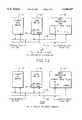
- FIGS. 1A and 1Bare functional block diagrams of two QIC-117 hardware bus standards and a peripheral device using the circuit of this invention from FIG. 3;
- FIG. 2is a chart comparing the two exemplary bus interface protocols illustrated in FIGS. 1A and 1B;
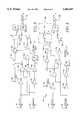
- FIG. 3is a functional circuit diagram of an illustrative embodiment of a dual interface driver circuit of this invention.
- FIG. 4is a functional circuit diagram of an alternative embodiment of a dual interface driver circuit of this invention.
- FIGS. 1A and 1Bshow two QIC-117 bus interface standards relevant to the illustrative dual interface driver circuit of this invention. These are the open collector TTL standard (FIG. 1A) and the tri-state CMOS standard (FIG. 1B), both further compared in FIG. 2.
- the host processor input bus 10interconnects the host processor 12, a floppy disk drive 14, a tape drive 16 and a plurality of other peripherals (not shown). These elements are also interconnected through a host processor output bus 18.
- a host processor CMOS input bus 20interconnects host processor 22, a floppy disk drive 24, tape drive 16 and a plurality of other peripheral devices (not shown). These elements are also interconnected by a host processor output bus 28.
- the primary distinctions between the open collector TTL and tri-state CMOS bus standardsare the active output current requirements and the input signal hysteresis specification.
- the TTL bus terminating resistor R tis substantially different from the equivalent CMOS bus terminating resistor R c in FIG. 1B. These differences reflect the different current-sinking requirements specified for the two exemplary bus protocols.
- a dual interface driver circuit 30 of this inventionis installed typically at the output of tape drive 16 as shown in FIGS. 1A and 1B. Dual interface driver 30 permits tape drive 16 to be connected to either bus 10 in FIG. 1A or bus 20 in FIG. 1B without physical modification. Such is not the case for floppy disk drives 14 or 24 or any other peripheral devices known in the art.
- FIG. 3shows an illustrative embodiment of an exemplary dual interface driver 34 of this invention. It is preferably fabricated as a single monolithic integrated circuit.
- driver 34 in FIG. 3accepts an input data signal at an input terminal 36.
- the input data signalis a two-valued binary signal S, which is replicated at the output terminal 38 in modified form S'. That is, the voltage and current characteristics (source impedance) of signal S' at output terminal 38 is modified with respect to the same characteristics of signal S at input terminal 36.
- the two exemplary interface protocols of driver 34 in FIG. 3are selected by a selection signal at an interface select terminal 40. Also, the output S' at output terminal 38 can be disabled by a disable signal at output disable terminal 42. Signals 40 and 42 are buffered by the inverters 44 and 46 and combined by the OR-gates 48 and 50 to create signals A and B according the following logic:
- the gated inverter 52, the inverter 54 and the OR-gate 56combine input signal S with signals A and B at the gate terminals of the MOSFETs 58 and 60.
- the gate signal on MOSFET 58is equal to input signal S unless signal B is high, which overrides S and forces MOSFET 58 off.
- the gate signals on Complimentary MOSFET 60are equal to input signal S unless signal A is high, which then overrides S and forces MOSFET 60 off.
- dual interface driver 34provides two output signal protocols associated with the source impedances provided in pads 62 and 64.
- a high binary signal at output disable terminal 42disables both such protocols.
- a low binary signal at interface selection terminal 40disables the protocol associated with pad 64 and a high binary signal at terminal 40 disables the other protocol associated with pad 62.
- a multiple interface driver for more than two interfacescan be understood as an extension of dual driver 34 to several interface protocols, each having signal means for disabling the protocol when it is not needed.
- FIG. 4An alternative embodiment 72 of a dual interface driver circuit of this invention is shown in FIG. 4.
- the essential feature of dual interface driver circuit 72is that only one output signal protocol is supplied; that one associated with the pad 74.
- the single protocolcan be modified by switching in an external pullup resistor R selected to modify the protocol in pad 74 as desired.
- pullup resistor Rcan be selected by external means from a plurality of such resistors each representing one of several protocols.
- MOSFET 76must be sufficient to drive both the signal terminating pullup resistor (not shown) and the selected local pullup resistor R.
- dual driver 72operates similarly to dual driver 34 in FIG. 3.
- the signals at interface selection terminal 40 and output disable terminal 42are buffered in inverters 44 and 46 and combined in OR-gate 48 to create the signal C according to the following logic:
- the inverter 78 and the OR-gate 80combine input signal S and signal C to produce a signal at the line 82 that forces MOSFET 76 off whenever signal C is high.
- a high value for signal Cremoves the external pullup network 84 from the circuit, forcing selection of the protocol associated with pad 74.
- pullup network 84is added to the dual driver circuit 72, modifying the protocol associated with pad 74 in a manner that depends on the value of pullup resistor R.
- interface selection terminal 40when interface selection terminal 40 is low, external pullup network 84 is disabled.
- external pullup network 84When terminal 40 is high, external pullup network 84 is added to modify the protocol associated with pad 74.
- output disable terminal 42When output disable terminal 42 is high, MOSFET 58 is forced off, thereby disabling the S' output at output terminal 38. Any of several protocols may be matched by selecting one of several pullup resistors provided by external means.
Landscapes
- Engineering & Computer Science (AREA)
- General Engineering & Computer Science (AREA)
- Theoretical Computer Science (AREA)
- Computer Hardware Design (AREA)
- Physics & Mathematics (AREA)
- General Physics & Mathematics (AREA)
- Logic Circuits (AREA)
Abstract
Description
A=disable or not select
B=disable or select
C=disable or not select
Claims (16)
Priority Applications (1)
| Application Number | Priority Date | Filing Date | Title |
|---|---|---|---|
| US07/950,939US5566347A (en) | 1992-09-24 | 1992-09-24 | Multiple interface driver circuit for a peripheral storage device |
Applications Claiming Priority (1)
| Application Number | Priority Date | Filing Date | Title |
|---|---|---|---|
| US07/950,939US5566347A (en) | 1992-09-24 | 1992-09-24 | Multiple interface driver circuit for a peripheral storage device |
Publications (1)
| Publication Number | Publication Date |
|---|---|
| US5566347Atrue US5566347A (en) | 1996-10-15 |
Family
ID=25491059
Family Applications (1)
| Application Number | Title | Priority Date | Filing Date |
|---|---|---|---|
| US07/950,939Expired - LifetimeUS5566347A (en) | 1992-09-24 | 1992-09-24 | Multiple interface driver circuit for a peripheral storage device |
Country Status (1)
| Country | Link |
|---|---|
| US (1) | US5566347A (en) |
Cited By (3)
| Publication number | Priority date | Publication date | Assignee | Title |
|---|---|---|---|---|
| US5787307A (en)* | 1994-11-18 | 1998-07-28 | International Business Machines Corporation | Apparatus for draining off electric charges from a bus connector pins having a switch controller for controlling two switches where the second switch connects the pins to ground |
| US5966306A (en)* | 1997-07-07 | 1999-10-12 | Motorola Inc. | Method for verifying protocol conformance of an electrical interface |
| US6145046A (en)* | 1997-11-18 | 2000-11-07 | Shuttle Technology Group Ltd. | Universal memory card interface apparatus |
Citations (7)
| Publication number | Priority date | Publication date | Assignee | Title |
|---|---|---|---|---|
| US3846763A (en)* | 1974-01-04 | 1974-11-05 | Honeywell Inf Systems | Method and apparatus for automatic selection of translators in a data processing system |
| US4790762A (en)* | 1985-07-23 | 1988-12-13 | Honeywell Inc. | Backplane for a modularly expandable programmable controller |
| US4936785A (en)* | 1988-12-19 | 1990-06-26 | Krug Eric M | Interchangeable adapter module for electronic devices |
| US4984202A (en)* | 1989-03-20 | 1991-01-08 | Hitachi, Ltd. | Low voltage-operated semiconductor integrated circuit |
| US5027315A (en)* | 1984-09-28 | 1991-06-25 | Advanced Micro Devices, Inc. | Programmable logic array using internally generated dynamic logic signals as selection signals for controlling its functions |
| US5036224A (en)* | 1990-03-01 | 1991-07-30 | National Semiconductor Corporation | Single ended MOS to ECL output buffer |
| US5043938A (en)* | 1988-12-29 | 1991-08-27 | Intel Corporation | Node controller for a local area network |
- 1992
- 1992-09-24USUS07/950,939patent/US5566347A/ennot_activeExpired - Lifetime
Patent Citations (7)
| Publication number | Priority date | Publication date | Assignee | Title |
|---|---|---|---|---|
| US3846763A (en)* | 1974-01-04 | 1974-11-05 | Honeywell Inf Systems | Method and apparatus for automatic selection of translators in a data processing system |
| US5027315A (en)* | 1984-09-28 | 1991-06-25 | Advanced Micro Devices, Inc. | Programmable logic array using internally generated dynamic logic signals as selection signals for controlling its functions |
| US4790762A (en)* | 1985-07-23 | 1988-12-13 | Honeywell Inc. | Backplane for a modularly expandable programmable controller |
| US4936785A (en)* | 1988-12-19 | 1990-06-26 | Krug Eric M | Interchangeable adapter module for electronic devices |
| US5043938A (en)* | 1988-12-29 | 1991-08-27 | Intel Corporation | Node controller for a local area network |
| US4984202A (en)* | 1989-03-20 | 1991-01-08 | Hitachi, Ltd. | Low voltage-operated semiconductor integrated circuit |
| US5036224A (en)* | 1990-03-01 | 1991-07-30 | National Semiconductor Corporation | Single ended MOS to ECL output buffer |
Cited By (3)
| Publication number | Priority date | Publication date | Assignee | Title |
|---|---|---|---|---|
| US5787307A (en)* | 1994-11-18 | 1998-07-28 | International Business Machines Corporation | Apparatus for draining off electric charges from a bus connector pins having a switch controller for controlling two switches where the second switch connects the pins to ground |
| US5966306A (en)* | 1997-07-07 | 1999-10-12 | Motorola Inc. | Method for verifying protocol conformance of an electrical interface |
| US6145046A (en)* | 1997-11-18 | 2000-11-07 | Shuttle Technology Group Ltd. | Universal memory card interface apparatus |
Similar Documents
| Publication | Publication Date | Title |
|---|---|---|
| US6040714A (en) | Method for providing two modes of I/O pad termination | |
| US6691201B1 (en) | Dual mode USB-PS/2 device | |
| US6185642B1 (en) | Bus for high frequency operation with backward compatibility and hot-plug ability | |
| US6484222B1 (en) | System for incorporating multiple expansion slots in a variable speed peripheral bus | |
| US7868656B2 (en) | Hot plug control apparatus and method | |
| US7375442B2 (en) | Interface circuit for providing a computer logic circuit with first and second voltages and an associated method | |
| US5305443A (en) | Microprocessor with low power bus | |
| US6327635B1 (en) | Add-on card with automatic bus power line selection circuit | |
| US4922449A (en) | Backplane bus system including a plurality of nodes | |
| US6693678B1 (en) | Data bus driver having first and second operating modes for coupling data to the bus at first and second rates | |
| US5361005A (en) | Configurable driver circuit and termination for a computer input/output bus | |
| US6037803A (en) | Integrated circuit having two modes of I/O pad termination | |
| US5751978A (en) | Multi-purpose peripheral bus driver apparatus and method | |
| US6438624B1 (en) | Configurable I/O expander addressing for I/O drawers in a multi-drawer rack server system | |
| US5146563A (en) | Node with coupling resistor for limiting current flow through driver during overlap condition | |
| KR100641744B1 (en) | High Speed Data Bus Driver | |
| US5566347A (en) | Multiple interface driver circuit for a peripheral storage device | |
| US20030105910A1 (en) | Bi-directional bus bridge in which multiple devices can assert bus concurrently | |
| US6693451B2 (en) | Input/output buffer capable of supporting a multiple of transmission logic buses | |
| US20040003162A1 (en) | Point-to-point electrical loading for a multi-drop bus | |
| US5446320A (en) | Circuit for clamping power output to ground while the computer is deactivated | |
| US6833733B2 (en) | Apparatus for improving bus capacity | |
| US6629171B2 (en) | Driving the last inbound signal on a line in a bus with a termination | |
| US6064254A (en) | High speed integrated circuit interconnection having proximally located active converter | |
| US7467252B2 (en) | Configurable I/O bus architecture |
Legal Events
| Date | Code | Title | Description |
|---|---|---|---|
| AS | Assignment | Owner name:ARCHIVE CORPORATION, CALIFORNIA Free format text:ASSIGNMENT OF ASSIGNORS INTEREST;ASSIGNOR:PATRICK, EDWARD H.;REEL/FRAME:006812/0374 Effective date:19931119 | |
| AS | Assignment | Owner name:CONNER PERIPHERALS, INC., CALIFORNIA Free format text:ASSIGNMENT OF ASSIGNORS INTEREST;ASSIGNOR:ARCHIVE CORPORATION;REEL/FRAME:007888/0687 Effective date:19931130 | |
| STCF | Information on status: patent grant | Free format text:PATENTED CASE | |
| AS | Assignment | Owner name:SEAGATE PERIPHERALS, INC., CALIFORNIA Free format text:CHANGE OF NAME;ASSIGNOR:CONNER PERIPHERALS, INC.;REEL/FRAME:008568/0400 Effective date:19960228 Owner name:SEAGATE TECHNOLOGY, INC., CALIFORNIA Free format text:MERGER;ASSIGNOR:SEAGATE PERIPHERALS,INC.;REEL/FRAME:008587/0277 Effective date:19970115 | |
| AS | Assignment | Owner name:SEAGATE PERIPHERALS, INC., CALIFORNIA Free format text:;ASSIGNOR:CONNER PERIPHERALS, INC.;REEL/FRAME:008545/0682 Effective date:19960228 | |
| FEPP | Fee payment procedure | Free format text:PAYER NUMBER DE-ASSIGNED (ORIGINAL EVENT CODE: RMPN); ENTITY STATUS OF PATENT OWNER: LARGE ENTITY Free format text:PAYOR NUMBER ASSIGNED (ORIGINAL EVENT CODE: ASPN); ENTITY STATUS OF PATENT OWNER: LARGE ENTITY | |
| FPAY | Fee payment | Year of fee payment:4 | |
| AS | Assignment | Owner name:SEAGATE TECHNOLOGY LLC, CALIFORNIA Free format text:ASSIGNMENT OF ASSIGNORS INTEREST;ASSIGNOR:SEAGATE TECHNOLOGY, INC.;REEL/FRAME:011077/0319 Effective date:20000728 | |
| AS | Assignment | Owner name:THE CHASE MANHATTAN BANK, AS COLLATERAL AGENT, NEW Free format text:SECURITY AGREEMENT;ASSIGNOR:SEAGATE TECHNOLOGY LLC;REEL/FRAME:011461/0001 Effective date:20001122 | |
| AS | Assignment | Owner name:JPMORGAN CHASE BANK, AS COLLATERAL AGENT, NEW YORK Free format text:SECURITY AGREEMENT;ASSIGNOR:SEAGATE TECHNOLOGY LLC;REEL/FRAME:013177/0001 Effective date:20020513 Owner name:JPMORGAN CHASE BANK, AS COLLATERAL AGENT,NEW YORK Free format text:SECURITY AGREEMENT;ASSIGNOR:SEAGATE TECHNOLOGY LLC;REEL/FRAME:013177/0001 Effective date:20020513 | |
| FPAY | Fee payment | Year of fee payment:8 | |
| AS | Assignment | Owner name:SEAGATE TECHNOLOGY LLC, CALIFORNIA Free format text:RELEASE OF SECURITY INTERESTS IN PATENT RIGHTS;ASSIGNOR:JPMORGAN CHASE BANK, N.A. (FORMERLY KNOWN AS THE CHASE MANHATTAN BANK AND JPMORGAN CHASE BANK), AS ADMINISTRATIVE AGENT;REEL/FRAME:016937/0554 Effective date:20051130 | |
| FPAY | Fee payment | Year of fee payment:12 | |
| REMI | Maintenance fee reminder mailed | ||
| AS | Assignment | Owner name:WELLS FARGO BANK, NATIONAL ASSOCIATION, AS COLLATERAL AGENT AND SECOND PRIORITY REPRESENTATIVE, CALIFORNIA Free format text:SECURITY AGREEMENT;ASSIGNORS:MAXTOR CORPORATION;SEAGATE TECHNOLOGY LLC;SEAGATE TECHNOLOGY INTERNATIONAL;REEL/FRAME:022757/0017 Effective date:20090507 Owner name:JPMORGAN CHASE BANK, N.A., AS ADMINISTRATIVE AGENT AND FIRST PRIORITY REPRESENTATIVE, NEW YORK Free format text:SECURITY AGREEMENT;ASSIGNORS:MAXTOR CORPORATION;SEAGATE TECHNOLOGY LLC;SEAGATE TECHNOLOGY INTERNATIONAL;REEL/FRAME:022757/0017 Effective date:20090507 Owner name:JPMORGAN CHASE BANK, N.A., AS ADMINISTRATIVE AGENT Free format text:SECURITY AGREEMENT;ASSIGNORS:MAXTOR CORPORATION;SEAGATE TECHNOLOGY LLC;SEAGATE TECHNOLOGY INTERNATIONAL;REEL/FRAME:022757/0017 Effective date:20090507 Owner name:WELLS FARGO BANK, NATIONAL ASSOCIATION, AS COLLATE Free format text:SECURITY AGREEMENT;ASSIGNORS:MAXTOR CORPORATION;SEAGATE TECHNOLOGY LLC;SEAGATE TECHNOLOGY INTERNATIONAL;REEL/FRAME:022757/0017 Effective date:20090507 | |
| AS | Assignment | Owner name:SEAGATE TECHNOLOGY LLC, CALIFORNIA Free format text:RELEASE;ASSIGNOR:JPMORGAN CHASE BANK, N.A., AS ADMINISTRATIVE AGENT;REEL/FRAME:025662/0001 Effective date:20110114 Owner name:SEAGATE TECHNOLOGY INTERNATIONAL, CALIFORNIA Free format text:RELEASE;ASSIGNOR:JPMORGAN CHASE BANK, N.A., AS ADMINISTRATIVE AGENT;REEL/FRAME:025662/0001 Effective date:20110114 Owner name:SEAGATE TECHNOLOGY HDD HOLDINGS, CALIFORNIA Free format text:RELEASE;ASSIGNOR:JPMORGAN CHASE BANK, N.A., AS ADMINISTRATIVE AGENT;REEL/FRAME:025662/0001 Effective date:20110114 Owner name:MAXTOR CORPORATION, CALIFORNIA Free format text:RELEASE;ASSIGNOR:JPMORGAN CHASE BANK, N.A., AS ADMINISTRATIVE AGENT;REEL/FRAME:025662/0001 Effective date:20110114 | |
| AS | Assignment | Owner name:THE BANK OF NOVA SCOTIA, AS ADMINISTRATIVE AGENT, CANADA Free format text:SECURITY AGREEMENT;ASSIGNOR:SEAGATE TECHNOLOGY LLC;REEL/FRAME:026010/0350 Effective date:20110118 Owner name:THE BANK OF NOVA SCOTIA, AS ADMINISTRATIVE AGENT, Free format text:SECURITY AGREEMENT;ASSIGNOR:SEAGATE TECHNOLOGY LLC;REEL/FRAME:026010/0350 Effective date:20110118 | |
| AS | Assignment | Owner name:SEAGATE TECHNOLOGY US HOLDINGS, INC., CALIFORNIA Free format text:TERMINATION AND RELEASE OF SECURITY INTEREST IN PATENT RIGHTS;ASSIGNOR:WELLS FARGO BANK, NATIONAL ASSOCIATION, AS COLLATERAL AGENT AND SECOND PRIORITY REPRESENTATIVE;REEL/FRAME:030833/0001 Effective date:20130312 Owner name:EVAULT INC. (F/K/A I365 INC.), CALIFORNIA Free format text:TERMINATION AND RELEASE OF SECURITY INTEREST IN PATENT RIGHTS;ASSIGNOR:WELLS FARGO BANK, NATIONAL ASSOCIATION, AS COLLATERAL AGENT AND SECOND PRIORITY REPRESENTATIVE;REEL/FRAME:030833/0001 Effective date:20130312 Owner name:SEAGATE TECHNOLOGY LLC, CALIFORNIA Free format text:TERMINATION AND RELEASE OF SECURITY INTEREST IN PATENT RIGHTS;ASSIGNOR:WELLS FARGO BANK, NATIONAL ASSOCIATION, AS COLLATERAL AGENT AND SECOND PRIORITY REPRESENTATIVE;REEL/FRAME:030833/0001 Effective date:20130312 Owner name:SEAGATE TECHNOLOGY INTERNATIONAL, CAYMAN ISLANDS Free format text:TERMINATION AND RELEASE OF SECURITY INTEREST IN PATENT RIGHTS;ASSIGNOR:WELLS FARGO BANK, NATIONAL ASSOCIATION, AS COLLATERAL AGENT AND SECOND PRIORITY REPRESENTATIVE;REEL/FRAME:030833/0001 Effective date:20130312 | |
| AS | Assignment | Owner name:SEAGATE TECHNOLOGY PUBLIC LIMITED COMPANY, CALIFORNIA Free format text:RELEASE BY SECURED PARTY;ASSIGNOR:THE BANK OF NOVA SCOTIA;REEL/FRAME:072193/0001 Effective date:20250303 Owner name:SEAGATE TECHNOLOGY, CALIFORNIA Free format text:RELEASE BY SECURED PARTY;ASSIGNOR:THE BANK OF NOVA SCOTIA;REEL/FRAME:072193/0001 Effective date:20250303 Owner name:SEAGATE TECHNOLOGY HDD HOLDINGS, CALIFORNIA Free format text:RELEASE BY SECURED PARTY;ASSIGNOR:THE BANK OF NOVA SCOTIA;REEL/FRAME:072193/0001 Effective date:20250303 Owner name:I365 INC., CALIFORNIA Free format text:RELEASE BY SECURED PARTY;ASSIGNOR:THE BANK OF NOVA SCOTIA;REEL/FRAME:072193/0001 Effective date:20250303 Owner name:SEAGATE TECHNOLOGY LLC, CALIFORNIA Free format text:RELEASE BY SECURED PARTY;ASSIGNOR:THE BANK OF NOVA SCOTIA;REEL/FRAME:072193/0001 Effective date:20250303 Owner name:SEAGATE TECHNOLOGY INTERNATIONAL, CAYMAN ISLANDS Free format text:RELEASE BY SECURED PARTY;ASSIGNOR:THE BANK OF NOVA SCOTIA;REEL/FRAME:072193/0001 Effective date:20250303 Owner name:SEAGATE HDD CAYMAN, CAYMAN ISLANDS Free format text:RELEASE BY SECURED PARTY;ASSIGNOR:THE BANK OF NOVA SCOTIA;REEL/FRAME:072193/0001 Effective date:20250303 Owner name:SEAGATE TECHNOLOGY (US) HOLDINGS, INC., CALIFORNIA Free format text:RELEASE BY SECURED PARTY;ASSIGNOR:THE BANK OF NOVA SCOTIA;REEL/FRAME:072193/0001 Effective date:20250303 |