US5566111A - Method for programming a nonvolatile memory - Google Patents
Method for programming a nonvolatile memoryDownload PDFInfo
- Publication number
- US5566111A US5566111AUS08/542,651US54265195AUS5566111AUS 5566111 AUS5566111 AUS 5566111AUS 54265195 AUS54265195 AUS 54265195AUS 5566111 AUS5566111 AUS 5566111A
- Authority
- US
- United States
- Prior art keywords
- voltage
- programming
- drain
- memory cell
- source
- Prior art date
- Legal status (The legal status is an assumption and is not a legal conclusion. Google has not performed a legal analysis and makes no representation as to the accuracy of the status listed.)
- Expired - Lifetime
Links
- 238000000034methodMethods0.000titleclaimsabstractdescription63
- 230000015654memoryEffects0.000titleclaimsabstractdescription53
- 238000012544monitoring processMethods0.000claimsabstractdescription20
- 108091006146ChannelsProteins0.000description15
- 230000008569processEffects0.000description8
- 238000010586diagramMethods0.000description7
- 230000007423decreaseEffects0.000description6
- 238000009826distributionMethods0.000description6
- 230000007246mechanismEffects0.000description5
- 239000004065semiconductorSubstances0.000description5
- 239000000758substrateSubstances0.000description5
- 230000008878couplingEffects0.000description4
- 238000010168coupling processMethods0.000description4
- 238000005859coupling reactionMethods0.000description4
- 230000005641tunnelingEffects0.000description4
- 238000012795verificationMethods0.000description4
- 238000002347injectionMethods0.000description3
- 239000007924injectionSubstances0.000description3
- 239000002800charge carrierSubstances0.000description2
- 230000005684electric fieldEffects0.000description2
- 238000004519manufacturing processMethods0.000description2
- 238000012986modificationMethods0.000description2
- 230000004048modificationEffects0.000description2
- 238000012856packingMethods0.000description2
- 238000003860storageMethods0.000description2
- 102000004129N-Type Calcium ChannelsHuman genes0.000description1
- 108090000699N-Type Calcium ChannelsProteins0.000description1
- 238000010276constructionMethods0.000description1
- 230000001419dependent effectEffects0.000description1
- 238000001514detection methodMethods0.000description1
- 239000012535impuritySubstances0.000description1
- 238000005468ion implantationMethods0.000description1
- 230000002093peripheral effectEffects0.000description1
- 230000004044responseEffects0.000description1
- 230000001960triggered effectEffects0.000description1
Images


Classifications
- G—PHYSICS
- G11—INFORMATION STORAGE
- G11C—STATIC STORES
- G11C16/00—Erasable programmable read-only memories
- G11C16/02—Erasable programmable read-only memories electrically programmable
- G11C16/06—Auxiliary circuits, e.g. for writing into memory
- G—PHYSICS
- G11—INFORMATION STORAGE
- G11C—STATIC STORES
- G11C16/00—Erasable programmable read-only memories
- G11C16/02—Erasable programmable read-only memories electrically programmable
- G11C16/06—Auxiliary circuits, e.g. for writing into memory
- G11C16/34—Determination of programming status, e.g. threshold voltage, overprogramming or underprogramming, retention
- G11C16/3436—Arrangements for verifying correct programming or erasure
- G11C16/3468—Prevention of overerasure or overprogramming, e.g. by verifying whilst erasing or writing
- G11C16/3486—Circuits or methods to prevent overprogramming of nonvolatile memory cells, e.g. by detecting onset or cessation of current flow in cells and using the detector output to terminate programming
- G—PHYSICS
- G11—INFORMATION STORAGE
- G11C—STATIC STORES
- G11C11/00—Digital stores characterised by the use of particular electric or magnetic storage elements; Storage elements therefor
- G11C11/56—Digital stores characterised by the use of particular electric or magnetic storage elements; Storage elements therefor using storage elements with more than two stable states represented by steps, e.g. of voltage, current, phase, frequency
- G11C11/5621—Digital stores characterised by the use of particular electric or magnetic storage elements; Storage elements therefor using storage elements with more than two stable states represented by steps, e.g. of voltage, current, phase, frequency using charge storage in a floating gate
- G11C11/5628—Programming or writing circuits; Data input circuits
- G11C11/5635—Erasing circuits
- G—PHYSICS
- G11—INFORMATION STORAGE
- G11C—STATIC STORES
- G11C16/00—Erasable programmable read-only memories
- G11C16/02—Erasable programmable read-only memories electrically programmable
- G11C16/06—Auxiliary circuits, e.g. for writing into memory
- G11C16/10—Programming or data input circuits
- G—PHYSICS
- G11—INFORMATION STORAGE
- G11C—STATIC STORES
- G11C16/00—Erasable programmable read-only memories
- G11C16/02—Erasable programmable read-only memories electrically programmable
- G11C16/06—Auxiliary circuits, e.g. for writing into memory
- G11C16/34—Determination of programming status, e.g. threshold voltage, overprogramming or underprogramming, retention
- G11C16/3436—Arrangements for verifying correct programming or erasure
- G11C16/3468—Prevention of overerasure or overprogramming, e.g. by verifying whilst erasing or writing
- G—PHYSICS
- G11—INFORMATION STORAGE
- G11C—STATIC STORES
- G11C2211/00—Indexing scheme relating to digital stores characterized by the use of particular electric or magnetic storage elements; Storage elements therefor
- G11C2211/56—Indexing scheme relating to G11C11/56 and sub-groups for features not covered by these groups
- G11C2211/562—Multilevel memory programming aspects
- G11C2211/5624—Concurrent multilevel programming and programming verification
Definitions
- the present inventionrelates to a method for programming a memory, and more particularly, to a method for programming a nonvolatile semiconductor memory.
- nonvolatile semiconductor memoriessuch as electrically erasable and programmable read-only memories (EEPROMs) and flash EEPROMs, intended as mass storage media possess an excessive cost per bit.
- EEPROMselectrically erasable and programmable read-only memories
- flash EEPROMsintended as mass storage media possess an excessive cost per bit.
- the packing density of a nonvolatile memorycorresponds with the number of memory cells on a one-to-one basis.
- a multibit cellstores at least two data bits in a single memory cell, thereby significantly increasing the storage packing density of the data in the same chip area without reducing a memory cell size.
- respective threshold voltage levelshave a statistical distribution of approximately 0.5 V. Consequently, as the distribution decreases by accurately adjusting the respective threshold levels, more levels can be programmed allowing the number of bits per cell to be increased.
- a technique for repeatedly programming and verifyinghas generally been used in the programming.
- a series of voltage pulsesis applied to a cell to program a nonvolatile memory cell at a desired threshold level.
- a reading process between the respective voltage pulsesverifies whether the cell reaches the desired threshold level.
- the programming processstops.
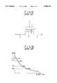
- FIG. 1Ashows the symbol and circuit diagram of the EEPROM of Cernea.
- the EEPROM cellconsists of a control gate 1, a floating gate 2, a source 3, a channel region 4, and a drain 5.
- the programming stateis automatically verified at the same time as the programming to slightly counteract the drawbacks of repeatedly programming and verification.
- the threshold voltage level applied to control gate 1 of the memory cellis not adjusted.
- U.S. Pat. No. 5,043,940 to Harariperforms the multilevel programming by changing reference currents corresponding to respective levels. As shown in FIG. 1B, the reference currents for verification are not explicitly or linearly related to the threshold voltages of a cell. Therefore, the multilevel cannot be directly and effectively controlled in the current-controlled method.
- the present inventionis directed to a method for programming a nonvolatile memory that substantially obviates one or more of the problems due to limitations and disadvantages of the related art.
- An object of the present inventionis to provide a method for programming a nonvolatile memory capable of simultaneously verifying threshold levels during the execution of two-level or multilevel programming.
- Another object of the present inventionis to provide a method for programming nonvolatile memory for adjusting respective threshold levels with voltages applied to a control gate during the execution of two-level or multilevel programming, in which respective threshold levels and the voltage applied to the control gate corresponding to respective threshold levels are linearly related.
- a method for programming a nonvolatile memory cell having a control gate, a floating gate, a drain, a source, and a channel region disposed between the drain and sourceincluding the steps of applying a first voltage to the control gate to form an inversion layer in the channel region, the first voltage being varied to program at least two threshold levels of the memory cell, applying a second voltage to the drain and a third voltage to the source, the second voltage being greater than the third voltage, monitoring a current flowing between the drain and the source during the programming of the at least two threshold levels, and terminating any one of the first voltage, the second voltage, and the third voltage when the monitored current reaches a preset reference current to thereby stop the programming of the at least two threshold levels.
- a nonvolatile memory cellsuch as an EEPROM cell, according to the present invention includes a control gate, a floating gate, a drain, a source and a channel region disposed between the drain and source.
- a preferred programming method of the present inventionis performed by applying a first voltage varied corresponding to the respective threshold levels during a programming of at least two threshold levels of the control gate for programming the EEPROM cell and forming an inversion layer in the channel region. Thereafter, a second voltage and a third voltage are applied to the drain and source, respectively, in such a manner that the voltage applied to the drain is higher than that applied to the source.
- FIG. 1Ais a circuit diagram of a general nonvolatile memory cell
- FIG. 1Bis a graph illustrating an automatic verification programming principle of the nonvolatile memory cell of FIG. 1A;
- FIG. 2is a diagram illustrating a programming method using a current detection according to an embodiment of the present invention
- FIGS. 3A to 3Gare waveform diagrams for respective nodes of FIG. 2;
- FIG. 4is a flowchart of the two-level or multilevel programming process according to a preferred embodiment of the present invention.
- FIG. 5Ais an equivalent circuit diagram of the nonvolatile memory cell shown in FIG. 1A illustrating the capacitance
- FIG. 5Bis a graph of the relationship between the threshold levels to be programmed and the corresponding control gate voltages.
- FIG. 5Cis a plot of the drain current variation from the start to the completion of the programming for the respective levels.
- FIG. 2is a diagram showing the construction of a nonvolatile memory device for describing a programming method according to the present invention.
- the nonvolatile memory device shown in FIG. 2comprises a first voltage source 6, a second voltage source 7, a third voltage source 8, a current detector 9, and an EEPROM cell 10.
- Psdesignates an externally-supplied programming start signal
- V STdesignates a programming stop signal.
- FIG. 1Ashows the most general structure of the EEPROM cell 10.
- the typical nonvolatile memory cell of a variety of typessuch as a simple stacked gate and a split-channel structure, can be simplified in an operational programming mode resulting in the structure shown in FIG. 1A.
- Second voltage source 7supplies a voltage V D to a drain 5 and third voltage source 8 supplies a voltage V S to a source 3.
- any valuecan be applied as voltage V S , but ground is assumed for voltage V S for convenience of explanation.
- I D ,i (t)designates a current flowing to drain 5.
- Current detector 9has a reference current value I REF , and generates programming stop signal V ST when current I D ,i (t) flowing through drain 5 reaches reference current I REF during the programming of the ith threshold level.
- Time t p ,idenotes an ending time of the ith threshold level programming.
- reference current I REF of current detector 9is determined by an electrical characteristic of EEPROM cell 10 which utilizes the programming method according to the present invention.
- drain current I D ,i (t)depends on time.
- This current value I D ,i (t)denotes the current value at drain 5 triggered by a voltage V F ,i (t) at floating gate 2 during the ith level programming.
- the current I D ,i (t)is at a maximum at the beginning of the period of the programming and decreases as the programming proceeds.
- program stop signal V STis generated from current detector 9 when it decreases below the reference current I REF of current detector 9.
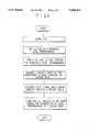
- FIGS. 3A to 3Gshow waveforms at respective nodes of FIG. 2, and FIG. 4 is a flow chart showing the two-level or multilevel programming process according to the present invention.
- the method for programming the EEPROM cell 10 of FIG. 2 according to the present inventionwill now be described in detail with reference to the flow chart of FIG. 4.
- a first voltagewhich is varied to correspond to every threshold level programming during the programming of at least two threshold levels, is applied to control gate 1, and a second voltage and a third voltage are applied to drain 5 and source 3, respectively, such that the voltage applied to drain 5 is greater than that applied to source 3. Then, the current flowing between drain 5 and source 3 is monitored while programming the respective threshold levels of EEPROM cell 10, and the supply of any one among the first, second, and third voltages respectively applied to control gate 1, drain 5, and source 3 is terminated to stop the programming when the current reaches a predetermined reference current.
- a corresponding cellis under an erased state prior to performing the programming.
- the erased statedenotes a zero level which is the lowest level.
- a floating gate FEThas a structure with an n-type channel on a p-type substrate.
- voltage V C ,i applied to control gate 1is set for the ith level programming. While programming start signal Ps of FIG. 3A is supplied, voltages V C ,i shown in FIG. 3B and V D are supplied from first voltage source 6 and second voltage source 7 to control gate 1 and drain 5, respectively.
- floating gate 2is supplied with electrons for the ith threshold level programming.
- any program mechanismmay be used to supply the charge to floating gate 2, but generally, either a hot carrier injection or tunneling mechanism is used.
- current detector 9monitors drain current I D ,i (t) during the ith threshold level programming.
- the ith threshold level programmingis considered to be complete and programming stop signal V ST is output as shown in FIG. 3E.
- current detector 9monitors current I D ,i (t), which substantially, as shown in FIGS. 3C and 3G, can be described by monitoring the variation of the voltage or amount of charge at floating gate 2 during the programming.
- the floating gate voltagereaches a reference voltage V F REF at floating gate 2 corresponding to reference current I REF when the drain current reaches reference current I REF .
- the monitoring of current I D ,i (t)can be described by monitoring the conductivity of the inversion layer formed in channel region 4 of FIG. 2.
- programming stop signal V STis provided to first and second voltage sources 6 and 7, and first and/or second voltage sources 6 and 7 stop the supply of voltages V C ,i and V D to control gate 1 and drain 5 in response to programming stop signal V ST as shown in FIG. 3B.
- FIG. 3Frepresents the variation of threshold voltages V C TH ,1 and V C TH ,2 at control gate 1 with respect to the time for the programming of the first and second threshold levels. Also, FIG. 3F illustrates the increase of threshold voltage V C TH ,1 at control gate 1 as the degree of the level increases during the multilevel programming. This is obtained by increasing voltage V C ,i during the programming.
- the programming times t p ,1 and t p ,2 of the first and second levelsare different because of the different amounts of variation of the control gate voltage and threshold voltage corresponding to respective levels.
- FIG. 3Gis a plot of the charge variation at floating gate 2 from an initial charge amount Q F ,0 (0) at floating gate 2 to the charge amount Q F ,1 (t p ,1) when the first threshold level programming is complete and the charge amount Q F ,2 (t p ,2) when the second threshold level programming is complete, in case of the first and second threshold levels. As shown in FIG.
- FIG. 5Ais an equivalent circuit diagram showing the capacitance of the EEPROM cell of FIG. 1A.
- C Cdesignates a capacitance between control gate 1 and floating gate 2
- C Dis a capacitance between drain 5 and floating gate 2
- C Sis a capacitance between source (including the substrate) and floating gate 2.
- a sum C T of the capacitancescan be written as:
- coupling coefficients of each capacitanceare defined as:
- V C TH (t) at control gate 1is defined as:
- V C TH (t) in equation (4)designates a threshold voltage shift measured at control gate 1 at time t.
- Threshold voltage shift V C TH (t)denotes a threshold voltage measured at control gate 1 after being caused by the charge stored in floating gate 12.
- threshold voltage V F TH at floating gate 3is an inherent threshold voltage of the FET, consisting of floating gate 2, drain 5, and source 3 of FIG. 1.
- V F REFis determined by the manufacturing conditions of the FET, such as a channel ion implantation and the thickness of the gate insulating layer when fabricating the EEPROM cell shown in FIG. 1. Therefore, threshold voltage V F TH of floating gate 2 is always constant.
- threshold voltage V C TH of control gate 1is determined by the amount of charge Q F at floating gate 2.
- the programming of respective threshold levelsis forced to stop when voltage V F (t) at floating gate 2 reaches reference voltage V F REF at floating gate 2. That is, this point corresponds to the time that current I D (t) of drain 5 reaches reference current I REF , and also corresponds to time t p the programming is complete.
- V F (t p ) of floating gate 2 when the threshold level programming is completeis:
- control gate voltage V C and threshold voltage shift V C THare linear with respect to each other.
- respective drain voltage V D , source voltage V S , and reference voltage V F REFare fixed with respect to the programming of the respective levels.
- drain voltage V D and source voltage V Sare to have the same value at the ending point of the programming of the respective levels.
- drain voltage V D and source voltage V Smay be variables differing in accordance with the programming time, the above object can be obtained only by permitting the values to be equal at the ending point of the programming.
- control gate voltage V C of respective levelsmay be varied in accordance with time.
- the value of control gate voltage V C of respective levelsis the value of the ending point of the programming of respective levels.
- reference voltage V F REFis a constant and control gate voltage V C ,i increases as it reaches a higher level with respect to the programming of the respective levels
- initial value I D ,i (0) of the drain currentincreases as it reaches the higher level. This process is illustrated in FIG. 5C.
- the programming completion point of the respective levelsis varied according to the electrical characteristics of the memory cells and the voltages applied to the respective nodes.
- control gate voltage V c ,0 and reference current I REF at floating gate 2remain in equations (7) and (8) if the desired lowest level value V C TH ,0 drain voltage V D and source voltage V S of the selected memory cell are determined.
- drain voltage V D and source voltage V Sare constants
- reference voltage V F REFcorresponds to reference current value I REF on a one-to-one basis.
- the memory cellis adjusted to the desired lowest level value V C TH ,0 and voltages V C ,0, V D , and V S are applied to the memory cell. Then, initial drain current value I D ,0 (0) is measured which becomes the reference current value.
- voltage V C ,0is determined in consideration of the programming time and the maximum control gate voltage V c ,n-1. Once voltage V C ,0 is determined, the reference current value can be obtained by the above-described method. The reference current value can also be measured using several other methods.
- the value V1 of equation (7)is fixed with respect to the programming of respective levels. If the parameters of equation (7) are adjusted to vary the value V1 for the programming of the respective levels, control gate voltage V C ,i and the corresponding threshold voltage V C TH ,i have a nonlinear relationship as shown by equation (8). Therefore, the shift value of the control gate voltage and the shift value of the corresponding threshold voltage differ. In this case, reference current I REF is properly adjusted by a desired value for each level to enable the programming of the threshold voltage corresponding to each level. Only that, since control gate voltage V C ,i and the corresponding threshold voltage V C TH ,i have a nonlinear relationship, their relationship can be experimentally determined.
- the source voltageis grounded, and the drain voltage and control gate voltage are applied with a positive voltage sufficiently high enough to cause the programming by hot carrier injection. At this time, the current flows between drain 5 and source 3, and this programming current is monitored to stop the programming when the current reaches reference current I REF .
- a positive voltageis applied to control gate 1, and a negative (or zero) voltage is applied to drain 5 and source 3.
- a sufficient electrical fieldis imposed to cause tunneling between floating gate 2 and drain 5, source 3, or channel region 4.
- the drain voltageis greater than the source voltage thereby allowing the current to flow between drain 5 and source 3.
- the currentis monitored to stop the programming when the current reaches reference current I REF . If a negative voltage is applied to drain 5 or source 3, a smaller or equal voltage is applied to the substrate when drain 5 and source 3 are n-type semiconductor impurity regions and the substrate is a p-type semiconductor.
- the erased statedenotes the lowest threshold level, i.e., V C TH ,0.
- V C THthe lowest threshold level
- the threshold levels of all cells within a selected blockare erased to below level zero, i.e., below V C TH ,0.
- all selected cellsare programmed with the level zero value, i.e., the voltage of control gate 1 is V C ,0.
- the value of V c ,0can be set by a proper value as described above. Since the erasure state is attained by the above-stated programming mechanism in actual aspect, a problem of excessive erasure can be solved.
- the programming method according to the present invention as described abovehas the following advantages.
- respective threshold voltage levels and respective control gate voltages corresponding to themhave a linear relationship to each other, and the shift value of the threshold voltage is the same as the shift value of the control gate voltage, thereby enabling the accurate adjustment of the threshold voltage shift of respective levels.
- the EEPROM cellinherently performs programming and reading simultaneously, so that a separate circuit for verifying the programmed content is not required, and consequently the programming speed is increased.
- the accuracy of the multilevel programmingi.e., error distribution of the programmed threshold voltages
- the threshold voltage error distribution of respective levels of the nonvolatile memory according to the present inventionis not dependent on many programming/erasing cycles.
- programmingis performed independent of the trap of the charge, channel mobility, bit line resistance, and unstable or unpredictable electrical elements.
- the programming system of the nonvolatile memory according to the present inventionis a voltage-controlled method by means of the control gate voltage, multilevel programming can be performed more easily and accurately than the current-controlled method.
Landscapes
- Engineering & Computer Science (AREA)
- Computer Hardware Design (AREA)
- Read Only Memory (AREA)
- Non-Volatile Memory (AREA)
Abstract
Description
1. Field of the Invention
The present invention relates to a method for programming a memory, and more particularly, to a method for programming a nonvolatile semiconductor memory.
2. Discussion of the Related Art
Generally, nonvolatile semiconductor memories, such as electrically erasable and programmable read-only memories (EEPROMs) and flash EEPROMs, intended as mass storage media possess an excessive cost per bit. A study on a multibit cell has been currently carried out as a method to solve the above-mentioned problem.
The packing density of a nonvolatile memory corresponds with the number of memory cells on a one-to-one basis. A multibit cell stores at least two data bits in a single memory cell, thereby significantly increasing the storage packing density of the data in the same chip area without reducing a memory cell size.
In order to embody the multibit cell, more than three threshold voltage levels must be programmed for each memory cell. For example, in order to store two data bits per cell, respective cells become programmable by four threshold level steps, i.e., 22 =4. As a result, the four threshold level steps logically correspond to respective logic states of 00, 01, 10, and 11.
In the above-described multilevel programming, it is critical that respective threshold voltage levels have a statistical distribution of approximately 0.5 V. Consequently, as the distribution decreases by accurately adjusting the respective threshold levels, more levels can be programmed allowing the number of bits per cell to be increased.
To decrease the above voltage distribution, a technique for repeatedly programming and verifying has generally been used in the programming. In this technique, a series of voltage pulses is applied to a cell to program a nonvolatile memory cell at a desired threshold level. A reading process between the respective voltage pulses verifies whether the cell reaches the desired threshold level. During verification, when the verified threshold level value reaches the desired threshold level value, the programming process stops.
In the system for repeatedly programming and verifying, it is difficult to reduce the error distribution of the threshold levels due to a program voltage pulse width. Furthermore, the algorithm of repeatedly programming and verifying requires an additional circuit, thereby increasing the peripheral circuit area of a chip. Moreover, this method increases the programming time.
To eliminate the above-stated drawbacks, R. Cernea of SunDisk Co. introduced a simultaneous programming and verifying technique (U.S. Pat. No. 5,422,842). FIG. 1A shows the symbol and circuit diagram of the EEPROM of Cernea. The EEPROM cell consists of acontrol gate 1, afloating gate 2, asource 3, a channel region 4, and adrain 5.
When a voltage sufficient to cause programming is applied to controlgate 1 and drain 5, a current flows betweendrain 5 andsource 3. The current is compared to a given reference current to generate a programming completion signal when the current is equal to or less than the reference current. This process is illustrated in FIG. 1B.
In this technique, the programming state is automatically verified at the same time as the programming to slightly counteract the drawbacks of repeatedly programming and verification. However, the threshold voltage level applied tocontrol gate 1 of the memory cell is not adjusted.
U.S. Pat. No. 5,043,940 to Harari performs the multilevel programming by changing reference currents corresponding to respective levels. As shown in FIG. 1B, the reference currents for verification are not explicitly or linearly related to the threshold voltages of a cell. Therefore, the multilevel cannot be directly and effectively controlled in the current-controlled method.
Accordingly, the present invention is directed to a method for programming a nonvolatile memory that substantially obviates one or more of the problems due to limitations and disadvantages of the related art.
An object of the present invention is to provide a method for programming a nonvolatile memory capable of simultaneously verifying threshold levels during the execution of two-level or multilevel programming.
Another object of the present invention is to provide a method for programming nonvolatile memory for adjusting respective threshold levels with voltages applied to a control gate during the execution of two-level or multilevel programming, in which respective threshold levels and the voltage applied to the control gate corresponding to respective threshold levels are linearly related.
Additional features and advantages of the invention will be set forth in the description which follows, and in part will be apparent from the description, or may be learned by practice of the invention. The objectives and other advantages of the invention will be realized and attained by the structure particularly pointed out in the written description and claims hereof as well as the appended drawings.
To achieve these and other advantages and in accordance with the purpose of the invention, as embodied and broadly described, a method for programming a nonvolatile memory cell having a control gate, a floating gate, a drain, a source, and a channel region disposed between the drain and source is provided, the method including the steps of applying a first voltage to the control gate to form an inversion layer in the channel region, the first voltage being varied to program at least two threshold levels of the memory cell, applying a second voltage to the drain and a third voltage to the source, the second voltage being greater than the third voltage, monitoring a current flowing between the drain and the source during the programming of the at least two threshold levels, and terminating any one of the first voltage, the second voltage, and the third voltage when the monitored current reaches a preset reference current to thereby stop the programming of the at least two threshold levels.
A nonvolatile memory cell, such as an EEPROM cell, according to the present invention includes a control gate, a floating gate, a drain, a source and a channel region disposed between the drain and source. A preferred programming method of the present invention is performed by applying a first voltage varied corresponding to the respective threshold levels during a programming of at least two threshold levels of the control gate for programming the EEPROM cell and forming an inversion layer in the channel region. Thereafter, a second voltage and a third voltage are applied to the drain and source, respectively, in such a manner that the voltage applied to the drain is higher than that applied to the source. Then, current flowing between the drain and source is monitored while programming the respective threshold levels of the EEPROM cell, and the supply of any one among the first voltage, second voltage and third voltage respectively applied to the control gate, drain and source is terminated for stopping the programming when the monitored current reaches a preset reference current.
It is to be understood that both the foregoing general description and the following detailed description are exemplary and explanatory and are intended to provide further explanation of the invention as claimed.
The accompanying drawings, which are included to provide a further understanding of the invention and are incorporated in and constitute a part of this specification, illustrate embodiments of the invention and together with the description serve to explain the principles of the invention. In the drawings:
FIG. 1A is a circuit diagram of a general nonvolatile memory cell;
FIG. 1B is a graph illustrating an automatic verification programming principle of the nonvolatile memory cell of FIG. 1A;
FIG. 2 is a diagram illustrating a programming method using a current detection according to an embodiment of the present invention;
FIGS. 3A to 3G are waveform diagrams for respective nodes of FIG. 2;
FIG. 4 is a flowchart of the two-level or multilevel programming process according to a preferred embodiment of the present invention;
FIG. 5A is an equivalent circuit diagram of the nonvolatile memory cell shown in FIG. 1A illustrating the capacitance;
FIG. 5B is a graph of the relationship between the threshold levels to be programmed and the corresponding control gate voltages; and
FIG. 5C is a plot of the drain current variation from the start to the completion of the programming for the respective levels.
Reference will now be made in detail to the preferred embodiments of the present invention, examples of which are illustrated in the accompanying drawings.
FIG. 2 is a diagram showing the construction of a nonvolatile memory device for describing a programming method according to the present invention. The nonvolatile memory device shown in FIG. 2 comprises a first voltage source 6, asecond voltage source 7, athird voltage source 8, acurrent detector 9, and anEEPROM cell 10. Ps designates an externally-supplied programming start signal, and VST designates a programming stop signal. FIG. 1A shows the most general structure of theEEPROM cell 10. In other words, the typical nonvolatile memory cell of a variety of types, such as a simple stacked gate and a split-channel structure, can be simplified in an operational programming mode resulting in the structure shown in FIG. 1A.
First voltage source 6 supplies a voltage VC,i (where i=0, 1, 2, . . . and n-1) to acontrol gate 1 of theEEPROM cell 10 for programming an ith threshold level in a multilevel programming. Accordingly, voltage VC,i has a different value for each level.Second voltage source 7 supplies a voltage VD to adrain 5 andthird voltage source 8 supplies a voltage VS to asource 3. Here, any value can be applied as voltage VS, but ground is assumed for voltage VS for convenience of explanation.
ID,i (t) designates a current flowing to drain 5.Current detector 9 has a reference current value IREF, and generates programming stop signal VST when current ID,i (t) flowing throughdrain 5 reaches reference current IREF during the programming of the ith threshold level.
Time tp,i denotes an ending time of the ith threshold level programming. At this time, reference current IREF ofcurrent detector 9 is determined by an electrical characteristic ofEEPROM cell 10 which utilizes the programming method according to the present invention.
When current ID,i (t) ofdrain 5 is redefined, drain current ID,i (t) depends on time. This current value ID,i (t) denotes the current value atdrain 5 triggered by a voltage VF,i (t) at floatinggate 2 during the ith level programming. The current ID,i (t) is at a maximum at the beginning of the period of the programming and decreases as the programming proceeds. Also, program stop signal VST is generated fromcurrent detector 9 when it decreases below the reference current IREF ofcurrent detector 9.
Under the above-described conditions, a two-level or multilevel programming process will be described with reference to FIGS. 3 and 4. FIGS. 3A to 3G show waveforms at respective nodes of FIG. 2, and FIG. 4 is a flow chart showing the two-level or multilevel programming process according to the present invention. Hereinafter, the method for programming theEEPROM cell 10 of FIG. 2 according to the present invention will now be described in detail with reference to the flow chart of FIG. 4.
Forprogramming EEPROM cell 10 and forming an inversion layer in channel region 4, a first voltage, which is varied to correspond to every threshold level programming during the programming of at least two threshold levels, is applied to controlgate 1, and a second voltage and a third voltage are applied to drain 5 andsource 3, respectively, such that the voltage applied to drain 5 is greater than that applied tosource 3. Then, the current flowing betweendrain 5 andsource 3 is monitored while programming the respective threshold levels ofEEPROM cell 10, and the supply of any one among the first, second, and third voltages respectively applied to controlgate 1,drain 5, andsource 3 is terminated to stop the programming when the current reaches a predetermined reference current.
This method will be described in detail below. It is assumed that a corresponding cell is under an erased state prior to performing the programming. Here, the erased state denotes a zero level which is the lowest level. It is also assumed that a floating gate FET has a structure with an n-type channel on a p-type substrate.
First, as shown in FIG. 3A, when programming start signal Ps is externally provided for the two-level or multilevel programming, voltage VC,i applied to controlgate 1 is set for the ith level programming. While programming start signal Ps of FIG. 3A is supplied, voltages VC,i shown in FIG. 3B and VD are supplied from first voltage source 6 andsecond voltage source 7 to controlgate 1 anddrain 5, respectively.
In this operation, floatinggate 2 is supplied with electrons for the ith threshold level programming. Here, any program mechanism may be used to supply the charge to floatinggate 2, but generally, either a hot carrier injection or tunneling mechanism is used.
After voltages VC,i and VD are applied to controlgate 1 anddrain 5, respectively,current detector 9 is turned on to monitor the voltage variation at floatinggate 2. Once voltages VC,i and VD are applied to controlgate 1 anddrain 5, as shown in FIG. 3C, voltage VF,i (t) for the ith threshold level programming is imposed upon floatinggate 2, and the inversion layer is formed in channel region 4 of the FET. Actually, sincesource 3,drain 5, and channel region 4 are placed on a semiconductor substrate (not shown), the current flows fromdrain 5 tosource 3 via channel region 4 once the inversion layer is formed. At this time, current ID,i (t) flows to drain 5, which is at a maximum at the beginning of the period as shown in FIG. 3D, and the electrons are injected into floatinggate 2 along with the progression of the programming to decrease the floating gate voltage, so that current ID,i (t) also decreases.
As described above,current detector 9 monitors drain current ID,i (t) during the ith threshold level programming. When the monitored value reaches reference current IREF, as shown in FIG. 3D, the ith threshold level programming is considered to be complete and programming stop signal VST is output as shown in FIG. 3E. Here, it is described thatcurrent detector 9 monitors current ID,i (t), which substantially, as shown in FIGS. 3C and 3G, can be described by monitoring the variation of the voltage or amount of charge at floatinggate 2 during the programming.
That is, as shown in FIG. 3C, the floating gate voltage reaches a reference voltage VFREF at floatinggate 2 corresponding to reference current IREF when the drain current reaches reference current IREF. In addition, the monitoring of current ID,i (t) can be described by monitoring the conductivity of the inversion layer formed in channel region 4 of FIG. 2.
In FIG. 2, programming stop signal VST is provided to first andsecond voltage sources 6 and 7, and first and/orsecond voltage sources 6 and 7 stop the supply of voltages VC,i and VD to controlgate 1 anddrain 5 in response to programming stop signal VST as shown in FIG. 3B. In other words, if current ID,i (t) is less than reference current IREF at the time t=tp,i, the ith threshold level programming is completed. Therefore, time tp,i denotes the time of programming the ith threshold level.
FIG. 3F represents the variation of threshold voltages VCTH,1 and VCTH,2 atcontrol gate 1 with respect to the time for the programming of the first and second threshold levels. Also, FIG. 3F illustrates the increase of threshold voltage VCTH,1 atcontrol gate 1 as the degree of the level increases during the multilevel programming. This is obtained by increasing voltage VC,i during the programming. Here, the programming times tp,1 and tp,2 of the first and second levels are different because of the different amounts of variation of the control gate voltage and threshold voltage corresponding to respective levels.
On the other hand, FIG. 3G is a plot of the charge variation at floatinggate 2 from an initial charge amount QF,0 (0) at floatinggate 2 to the charge amount QF,1 (tp,1) when the first threshold level programming is complete and the charge amount QF,2 (tp,2) when the second threshold level programming is complete, in case of the first and second threshold levels. As shown in FIG. 3G, the charge amount at floatinggate 2 increases from the initial value QF,0 (0) to respective charge amounts QF,1 (tp,1) and QF,2 (tp,2) when voltages VF,1 (t) and VF,2 (t) (where t=tp,1 and t=tp,2) at floatinggate 2 reach reference voltage VFREF at floatinggate 2 corresponding to reference current IREF.
Referring to FIG. 5A, the relationship between voltage VC,i applied to controlgate 1 and the threshold voltage of the corresponding level will be described, which is one significant result of the present invention.
FIG. 5A is an equivalent circuit diagram showing the capacitance of the EEPROM cell of FIG. 1A. In FIG. 5A, CC designates a capacitance betweencontrol gate 1 and floatinggate 2, CD is a capacitance betweendrain 5 and floatinggate 2, and CS is a capacitance between source (including the substrate) and floatinggate 2.
A sum CT of the capacitances can be written as:
C.sub.T =C.sub.C +C.sub.D +C.sub.S (1)
Also, coupling coefficients of each capacitance are defined as:
α.sub.C =C.sub.C /C.sub.T, α.sub.D =C.sub.D /C.sub.T, α.sub.S =C.sub.S /C.sub.T (2)
In FIG. 5A, the voltage at floatinggate 2 during programming is generally written as: ##EQU1## where reference symbol QF (t) designates the charge amount at floatinggate 2 at time t. During programming, threshold voltage VCTH (t) atcontrol gate 1 is defined as:
V.sup.C.sub.TH (t)=-Q.sub.F (t)/C.sub.C (4)
In other words, VCTH (t) in equation (4) designates a threshold voltage shift measured atcontrol gate 1 at time t. Threshold voltage shift VCTH (t) denotes a threshold voltage measured atcontrol gate 1 after being caused by the charge stored in floating gate 12.
Also threshold voltage VFTH at floatinggate 3 is an inherent threshold voltage of the FET, consisting of floatinggate 2,drain 5, andsource 3 of FIG. 1. VFREF is determined by the manufacturing conditions of the FET, such as a channel ion implantation and the thickness of the gate insulating layer when fabricating the EEPROM cell shown in FIG. 1. Therefore, threshold voltage VFTH of floatinggate 2 is always constant.
However, threshold voltage VCTH ofcontrol gate 1 is determined by the amount of charge QF at floatinggate 2. The programming of respective threshold levels is forced to stop when voltage VF (t) at floatinggate 2 reaches reference voltage VFREF at floatinggate 2. That is, this point corresponds to the time that current ID (t) ofdrain 5 reaches reference current IREF, and also corresponds to time tp the programming is complete.
Thus, voltage VF (tp) of floatinggate 2 when the threshold level programming is complete is:
V.sub.F (t.sub.p)=V.sup.F.sub.REF =α.sub.C [V.sub.C -V.sup.C.sub.TH (t.sub.P)]+α.sub.D V.sub.D +α.sub.S V.sub.S (5)
By rearranging equation (5), voltage VC applied from first voltage source 6 to controlgate 1 is: ##EQU2## where:
V1=[V.sup.F.sub.REF -α.sub.D V.sub.D -α.sub.S V.sub.S ]/α.sub.C (7)
Here, by adjusting three parameters of drain voltage VD, source voltage VS, and reference voltage VFREF such that value V1 is fixed at the programming ending period of the respective level programming, control gate voltage VC and threshold voltage shift VCTH are linear with respect to each other. In the simplest method for making V1 fixed, respective drain voltage VD, source voltage VS, and reference voltage VFREF are fixed with respect to the programming of the respective levels.
However, as expressed in equation (5), drain voltage VD and source voltage VS are to have the same value at the ending point of the programming of the respective levels. In other words, although drain voltage VD and source voltage VS may be variables differing in accordance with the programming time, the above object can be obtained only by permitting the values to be equal at the ending point of the programming.
In equation (7), if coupling coefficients αD and αS are considerably smaller than coupling coefficient αC, the two terms involving coupling coefficients αD and αS may be ignored.
In equation (5), the value of control gate voltage VC of respective levels may be varied in accordance with time. In this case, the value of control gate voltage VC of respective levels is the value of the ending point of the programming of respective levels.
Value V1 is forced to be constant with respect to every programming level as described above so that control gate voltage VC,i required for the ith threshold level programming is expressed as equation (8) by means of equation (7):
V.sub.C,i =V.sub.TH,i +V1 (where i=0, 1, 2, 3 . . . , n-1) (8)
In view of equation (8), it can be realized that the threshold levels desired to be programmed and the control gate voltage applied corresponding to them have the linear relation with a slope of one. FIG. 5B illustrates the result. Here, it also can be noted from equation (4) that the charge amount of floatinggate 2 is linear with respect to the control gate voltages.
Since value V1 is constant as described above, an ith shift value ΔVC,i of the voltage applied to controlgate 1 during the multilevel programming is expressed as:
ΔV.sub.C,i =ΔV.sup.C.sub.TH,i (9)
From equations (8) and (9), when shift value ΔVCTH,i goes from the erased state, i.e., the lowest level, to one of the respective threshold levels determined during the two-level or multilevel programming, the programming of the corresponding level is performed so that a value, obtained by adding the desired threshold level shift value ΔVCTH,i to a value VC,0 of the previously known lowest level programming, is applied to the control gate voltage. One then waits for the automatic completion of the programming.
Here, since reference voltage VFREF is a constant and control gate voltage VC,i increases as it reaches a higher level with respect to the programming of the respective levels, the initial value ID,i (0) of the drain current increases as it reaches the higher level. This process is illustrated in FIG. 5C. Also, the programming completion point of the respective levels is varied according to the electrical characteristics of the memory cells and the voltages applied to the respective nodes.
A method for determining control gate voltage Vc,0 and reference current value IREF for performing the programming of the lowest level will now be described.
To begin, two parameters of control gate voltage Vc,0 and reference current IREF at floatinggate 2 remain in equations (7) and (8) if the desired lowest level value VCTH,0 drain voltage VD and source voltage VS of the selected memory cell are determined. Here, since drain voltage VD and source voltage VS are constants, reference voltage VFREF corresponds to reference current value IREF on a one-to-one basis.
The memory cell is adjusted to the desired lowest level value VCTH,0 and voltages VC,0, VD, and VS are applied to the memory cell. Then, initial drain current value ID,0 (0) is measured which becomes the reference current value. Here, voltage VC,0 is determined in consideration of the programming time and the maximum control gate voltage Vc,n-1. Once voltage VC,0 is determined, the reference current value can be obtained by the above-described method. The reference current value can also be measured using several other methods.
In the foregoing description, the value V1 of equation (7) is fixed with respect to the programming of respective levels. If the parameters of equation (7) are adjusted to vary the value V1 for the programming of the respective levels, control gate voltage VC,i and the corresponding threshold voltage VCTH,i have a nonlinear relationship as shown by equation (8). Therefore, the shift value of the control gate voltage and the shift value of the corresponding threshold voltage differ. In this case, reference current IREF is properly adjusted by a desired value for each level to enable the programming of the threshold voltage corresponding to each level. Only that, since control gate voltage VC,i and the corresponding threshold voltage VCTH,i have a nonlinear relationship, their relationship can be experimentally determined.
Moreover, the concept of the present invention described herein is explained regardless of the programming mechanism. Thus, it can be realized that the concept of the present invention is applicable to the programming mechanism of any system expressed by equation (3).
If the hot carrier injection system is employed, the source voltage is grounded, and the drain voltage and control gate voltage are applied with a positive voltage sufficiently high enough to cause the programming by hot carrier injection. At this time, the current flows betweendrain 5 andsource 3, and this programming current is monitored to stop the programming when the current reaches reference current IREF.
When the tunneling system is employed, a positive voltage is applied to controlgate 1, and a negative (or zero) voltage is applied to drain 5 andsource 3. As a result, a sufficient electrical field is imposed to cause tunneling between floatinggate 2 anddrain 5,source 3, or channel region 4. At this time, the drain voltage is greater than the source voltage thereby allowing the current to flow betweendrain 5 andsource 3. The current is monitored to stop the programming when the current reaches reference current IREF. If a negative voltage is applied to drain 5 orsource 3, a smaller or equal voltage is applied to the substrate whendrain 5 andsource 3 are n-type semiconductor impurity regions and the substrate is a p-type semiconductor.
Heretofore, the two-level or multilevel programming method is described. Hereinafter, an erasure method using the above programming system will be described.
In connection with the erasure, voltages are applied to respective nodes to impose an electric field strong enough to erase the charge carriers between floatinggate 2 andsource 3,drain 5, or channel region 4, thereby erasing the charge carriers tosource 3,drain 5, or channel region 4 through tunneling. According to the present invention, the erased state denotes the lowest threshold level, i.e., VCTH,0. In other words, all EEPROM cells within a given erasure block are programmed at the lowest level. Thus, the erasing process is easily carried out by the following steps.
First, the threshold levels of all cells within a selected block are erased to below level zero, i.e., below VCTH,0. Successively, all selected cells are programmed with the level zero value, i.e., the voltage ofcontrol gate 1 is VC,0. Here, the value of Vc,0 can be set by a proper value as described above. Since the erasure state is attained by the above-stated programming mechanism in actual aspect, a problem of excessive erasure can be solved.
The programming method according to the present invention as described above has the following advantages.
First, multilevel programming is easily executed since only the voltage of the control gate is changed for each programming of respective threshold levels.
Second, respective threshold voltage levels and respective control gate voltages corresponding to them have a linear relationship to each other, and the shift value of the threshold voltage is the same as the shift value of the control gate voltage, thereby enabling the accurate adjustment of the threshold voltage shift of respective levels.
Third, since the erased state is adjusted by an optional control gate voltage with the programming of the lowest level, there is essentially no problem of excessive erasure.
Fourth, the EEPROM cell inherently performs programming and reading simultaneously, so that a separate circuit for verifying the programmed content is not required, and consequently the programming speed is increased.
Fifth, a previous programming is not needed before executing the erasure.
Sixth, the accuracy of the multilevel programming, i.e., error distribution of the programmed threshold voltages, is accurately determined by the parameters fixed during the fabrication of the nonvolatile memory and application of the bias voltage. Therefore, the threshold voltage error distribution of respective levels of the nonvolatile memory according to the present invention is not dependent on many programming/erasing cycles. Furthermore, programming is performed independent of the trap of the charge, channel mobility, bit line resistance, and unstable or unpredictable electrical elements.
Seventh, since the programming system of the nonvolatile memory according to the present invention is a voltage-controlled method by means of the control gate voltage, multilevel programming can be performed more easily and accurately than the current-controlled method.
It will be apparent to those skilled in the art that various modifications and variations can be made in the method for programming a nonvolatile memory of the present invention without departing from the spirit or scope of the invention. Thus, it is intended that the present invention cover the modifications and variations of this invention provided they come within the scope of the appended claims and their equivalents.
Claims (19)
1. A method for programming a nonvolatile memory cell having a control gate, a floating gate, a drain, a source, and a channel region disposed between the drain and source, the method comprising the steps of:
applying a first voltage to the control gate to form an inversion layer in the channel region, the first voltage being varied to program at least two threshold levels of the memory cell;
applying a second voltage to the drain and a third voltage to the source, the second voltage being greater than the third voltage;
monitoring a current flowing between the drain and the source during the programming of the at least two threshold levels; and
terminating any one of the first voltage, the second voltage, and the third voltage when the monitored current reaches a preset reference current to thereby stop the programming of the at least two threshold levels.
2. The method for programming a nonvolatile memory cell according to claim 1, wherein the reference current has a fixed value during the programming of the at least two threshold levels.
3. A method for programming a nonvolatile memory cell having a control gate, a floating gate, a drain, and a source, the method comprising the steps of:
applying a variable first voltage to the control gate;
applying a second voltage to the drain and a third voltage to the source;
monitoring a current flowing between the drain and the source during application of the first voltage to the control gate; and
terminating application of any of the first voltage to the control gate, the second voltage to the drain, and the third voltage to the source when the monitored current reaches a reference current.
4. The method for programming a nonvolatile memory cell according to claim 3, wherein the step of monitoring the current includes the step of monitoring a voltage at the floating gate.
5. The method for programming a nonvolatile memory cell according to claim 3, wherein the step of monitoring the current includes the step of monitoring an amount of charge at the floating gate.
6. The method for programming a nonvolatile memory cell according to claim 3, wherein application of the first voltage to the control gate forms an inversion layer in a channel region disposed between the drain and the source.
7. The method for programming a nonvolatile memory cell according to claim 6, wherein the step of monitoring the current includes the step of monitoring a conductivity of the inversion layer.
8. The method for programming a nonvolatile memory cell according to claim 3, wherein the first voltage is varied linearly with respect to at least two threshold levels of the memory cell.
9. The method for programming a nonvolatile memory cell according to claim 3, wherein the second voltage is greater than the third voltage.
10. The method for programming a nonvolatile memory cell according to claim 3, wherein the reference current is a fixed reference current.
11. A method for programming at least two threshold levels of a nonvolatile memory cell, the memory cell having a control gate, a floating gate, a drain, and a source, the method comprising the steps of:
applying a first voltage to the control gate, the first voltage corresponding to a respective one of the at least two threshold levels;
applying a second voltage to the drain and a third voltage to the source;
monitoring a current flowing between the drain and the source during application of the first voltage to the control gate; and
terminating application of any of the first voltage to the control gate, the second voltage to the drain, and the third voltage to the source when the monitored current reaches a reference current.
12. The method for programming a nonvolatile memory cell according to claim 11, wherein the step of monitoring the current includes the step of monitoring a voltage at the floating gate.
13. The method for programming a nonvolatile memory cell according to claim 11, wherein the step of monitoring the current includes the step of monitoring an amount of charge at the floating gate.
14. The method for programming a nonvolatile memory cell according to claim 11, wherein application of the first voltage to the control gate forms an inversion layer in a channel region disposed between the drain and the source.
15. The method for programming a nonvolatile memory cell according to claim 14, wherein the step of monitoring the current includes the step of monitoring a conductivity of the inversion layer.
16. The method for programming a nonvolatile memory cell according to claim 11, wherein the first voltage is selected according to a linear relationship with the at least two threshold levels.
17. The method for programming a nonvolatile memory cell according to claim 11, wherein the second voltage is greater than the third voltage.
18. The method for programming a nonvolatile memory cell according to claim 11, wherein the reference current is a fixed reference current.
19. The method for programming a nonvolatile memory cell according to claim 11, wherein the reference current is a fixed reference current.
Applications Claiming Priority (2)
| Application Number | Priority Date | Filing Date | Title |
|---|---|---|---|
| KR1019950030440AKR0172831B1 (en) | 1995-09-18 | 1995-09-18 | How to Program Nonvolatile Memory |
| KR30440/1995 | 1995-09-18 |
Publications (1)
| Publication Number | Publication Date |
|---|---|
| US5566111Atrue US5566111A (en) | 1996-10-15 |
Family
ID=19427071
Family Applications (1)
| Application Number | Title | Priority Date | Filing Date |
|---|---|---|---|
| US08/542,651Expired - LifetimeUS5566111A (en) | 1995-09-18 | 1995-10-13 | Method for programming a nonvolatile memory |
Country Status (10)
| Country | Link |
|---|---|
| US (1) | US5566111A (en) |
| EP (1) | EP0763829B1 (en) |
| JP (1) | JP3211146B2 (en) |
| KR (1) | KR0172831B1 (en) |
| CN (1) | CN1104010C (en) |
| DE (1) | DE69636063T2 (en) |
| MY (1) | MY115787A (en) |
| RU (1) | RU2111555C1 (en) |
| SG (1) | SG68590A1 (en) |
| TW (1) | TW284884B (en) |
Cited By (32)
| Publication number | Priority date | Publication date | Assignee | Title |
|---|---|---|---|---|
| US5721705A (en)* | 1995-12-20 | 1998-02-24 | Hyundai Electronics Industries Co., Ltd. | Circuitry for controlling a threshold voltage in a flash memory cell |
| US5751632A (en)* | 1996-11-19 | 1998-05-12 | Lg Semicon Co., Ltd. | Device for and method of sensing data of multi-bit memory cell |
| US5768191A (en)* | 1995-12-07 | 1998-06-16 | Samsung Electronics Co., Ltd. | Methods of programming multi-state integrated circuit memory devices |
| US5801993A (en)* | 1996-10-01 | 1998-09-01 | Lg Semicon Co., Ltd. | Nonvolatile memory device |
| US5818759A (en)* | 1996-02-29 | 1998-10-06 | Sanyo Electric Co., Ltd. | Non-volatile semiconductor memory device |
| US5852578A (en)* | 1997-06-17 | 1998-12-22 | Hoang; Loc B. | Flash cell having self-timed programming |
| US5867427A (en)* | 1996-08-07 | 1999-02-02 | Nec Corporation | Electrically writable nonvolatile semiconductor memory device |
| US5870335A (en)* | 1997-03-06 | 1999-02-09 | Agate Semiconductor, Inc. | Precision programming of nonvolatile memory cells |
| US5892710A (en)* | 1994-01-21 | 1999-04-06 | Intel Corporation | Method and circuitry for storing discrete amounts of charge in a single memory element |
| US5907855A (en)* | 1996-10-15 | 1999-05-25 | Micron Technology, Inc. | Apparatus and method for reducing programming cycles for multistate memory system |
| US5909394A (en)* | 1998-08-24 | 1999-06-01 | Taiwan Semiconductor Manufacturing Co., Ltd. | Precharge circuit for preventing invalid output pulses caused by current sensing circuits in flash memory devices |
| US6016271A (en)* | 1997-08-29 | 2000-01-18 | Stmicroeletronics S.R.L. | Method and circuit for generating a gate voltage in non-volatile memory devices |
| US6038166A (en)* | 1998-04-01 | 2000-03-14 | Invox Technology | High resolution multi-bit-per-cell memory |
| US6046934A (en)* | 1999-01-12 | 2000-04-04 | Macronix International Co., Ltd. | Method and device for multi-level programming of a memory cell |
| EP0901128A3 (en)* | 1997-09-05 | 2000-04-26 | Information Storage Devices, Inc. | Method and apparatus for adjustment and control of an interactive method of recording analog signals with on chip selection of a voltage ramp amplitude |
| US6097639A (en)* | 1997-12-31 | 2000-08-01 | Lg Semicon Co., Ltd. | System and method for programming nonvolatile memory |
| US6141253A (en)* | 1997-08-26 | 2000-10-31 | Macronix International Co., Ltd. | Electrically programmable semiconductor device with concurrent program and verification operations |
| US6178118B1 (en) | 1997-08-26 | 2001-01-23 | Macronix International Co., Ltd. | Electrically programmable semiconductor device with multi-level wordline voltages for programming multi-level threshold voltages |
| US6212100B1 (en)* | 1996-07-23 | 2001-04-03 | Hyundai Electronics Industries Co., Ltd. | Nonvolatile memory cell and method for programming and/or verifying the same |
| US6278634B1 (en) | 1999-06-29 | 2001-08-21 | Hyundai Electronics Industries Co., Ltd. | Reference memory cell initialization circuit and method |
| US6282145B1 (en) | 1999-01-14 | 2001-08-28 | Silicon Storage Technology, Inc. | Array architecture and operating methods for digital multilevel nonvolatile memory integrated circuit system |
| US6396742B1 (en) | 2000-07-28 | 2002-05-28 | Silicon Storage Technology, Inc. | Testing of multilevel semiconductor memory |
| US6462986B1 (en) | 1995-10-06 | 2002-10-08 | Silicon Storage Technology, Inc. | Integrated circuit for storage and retrieval of multiple digital bits per nonvolatile memory cell |
| US6487116B2 (en) | 1997-03-06 | 2002-11-26 | Silicon Storage Technology, Inc. | Precision programming of nonvolatile memory cells |
| US20030151774A1 (en)* | 2002-02-13 | 2003-08-14 | Konica Corporation | Image processing device and image processing method |
| US20040008567A1 (en)* | 2002-07-12 | 2004-01-15 | Fujitsu Limited | Threshold voltage adjustment method of non-volatile semiconductor memory device and non-volatile semiconductor memory device |
| US6728825B1 (en) | 1996-10-15 | 2004-04-27 | Micron Technology, Inc. | Apparatus and method for reducing programming cycles for multistate memory system |
| US6903979B1 (en)* | 2003-09-17 | 2005-06-07 | National Semiconductor Corporation | Efficient method of PMOS stacked-gate memory cell programming utilizing feedback control of substrate current |
| US20060092706A1 (en)* | 2004-10-29 | 2006-05-04 | Spansion Llc | Semiconductor device and method for controlling the same |
| US7385843B2 (en) | 1997-08-07 | 2008-06-10 | Sandisk Corporation | Multi-state memory |
| US20080212357A1 (en)* | 2004-01-29 | 2008-09-04 | Campbell Kristy A | Simultaneous read circuit for multiple memory cells |
| US7778066B2 (en) | 2007-08-23 | 2010-08-17 | Samsung Electronics Co., Ltd. | Resistance variable memory device and programming method thereof |
Families Citing this family (15)
| Publication number | Priority date | Publication date | Assignee | Title |
|---|---|---|---|---|
| DE19545557A1 (en)* | 1995-12-06 | 1997-06-12 | Siemens Ag | Read-only memory and method for controlling the same |
| KR100521320B1 (en)* | 1997-11-25 | 2006-01-12 | 삼성전자주식회사 | Non volatile memory device and program method thereof |
| JPH11306775A (en) | 1998-04-17 | 1999-11-05 | Tadahiro Omi | Semiconductor memory device |
| US6088268A (en)* | 1998-09-17 | 2000-07-11 | Atmel Corporation | Flash memory array with internal refresh |
| JP3848064B2 (en) | 2000-08-07 | 2006-11-22 | シャープ株式会社 | Test method for semiconductor nonvolatile memory |
| KR100386296B1 (en)* | 2000-12-30 | 2003-06-02 | 주식회사 하이닉스반도체 | Circuit for programming and reading flash memory with multiple levels and method for the same |
| CN100543875C (en)* | 2004-09-01 | 2009-09-23 | 旺宏电子股份有限公司 | Programming method of nonvolatile memory |
| US7085168B2 (en)* | 2004-12-30 | 2006-08-01 | Macronix International Co., Ltd. | Programming method for controlling memory threshold voltage distribution |
| KR100780773B1 (en)* | 2006-11-03 | 2007-11-30 | 주식회사 하이닉스반도체 | Program start bias setting method of flash memory device and program method using the same |
| CN101373584B (en)* | 2007-08-21 | 2011-07-06 | 联咏科技股份有限公司 | source driver |
| US8369154B2 (en)* | 2010-03-24 | 2013-02-05 | Ememory Technology Inc. | Channel hot electron injection programming method and related device |
| US8467245B2 (en) | 2010-03-24 | 2013-06-18 | Ememory Technology Inc. | Non-volatile memory device with program current clamp and related method |
| JP2014049151A (en)* | 2012-08-30 | 2014-03-17 | Ememory Technology Inc | Flash memory |
| KR102535414B1 (en)* | 2016-05-17 | 2023-05-24 | 에스케이하이닉스 주식회사 | EPROM memory device for having a uniform program characteristics and method of programming the EPROM memory device |
| US11507816B2 (en)* | 2019-09-19 | 2022-11-22 | Silicon Storage Technology, Inc. | Precision tuning for the programming of analog neural memory in a deep learning artificial neural network |
Citations (8)
| Publication number | Priority date | Publication date | Assignee | Title |
|---|---|---|---|---|
| US4331968A (en)* | 1980-03-17 | 1982-05-25 | Mostek Corporation | Three layer floating gate memory transistor with erase gate over field oxide region |
| US5043940A (en)* | 1988-06-08 | 1991-08-27 | Eliyahou Harari | Flash EEPROM memory systems having multistate storage cells |
| US5047362A (en)* | 1988-08-11 | 1991-09-10 | Sgs-Thomson Microelectronics S.A. | Method of making large-scale EPROM memory with a checker board pattern and an improved coupling factor |
| US5163021A (en)* | 1989-04-13 | 1992-11-10 | Sundisk Corporation | Multi-state EEprom read and write circuits and techniques |
| US5268318A (en)* | 1988-06-08 | 1993-12-07 | Eliyahou Harari | Highly compact EPROM and flash EEPROM devices |
| US5386422A (en)* | 1991-03-12 | 1995-01-31 | Kabushiki Kaisha Toshiba | Electrically erasable and programmable non-volatile memory system with write-verify controller using two reference levels |
| US5394362A (en)* | 1991-02-08 | 1995-02-28 | Banks; Gerald J. | Electrically alterable non-voltatile memory with N-bits per memory cell |
| US5422842A (en)* | 1993-07-08 | 1995-06-06 | Sundisk Corporation | Method and circuit for simultaneously programming and verifying the programming of selected EEPROM cells |
Family Cites Families (6)
| Publication number | Priority date | Publication date | Assignee | Title |
|---|---|---|---|---|
| JPS60236195A (en)* | 1984-05-08 | 1985-11-22 | Nec Corp | Nonvolatile semiconductor memory |
| JPS626493A (en)* | 1985-06-29 | 1987-01-13 | Ricoh Co Ltd | Writable/readable semiconductor memory device |
| JPS6478494A (en)* | 1987-09-19 | 1989-03-23 | Mitsubishi Electric Corp | Nonvolatile semiconductor memory |
| JPH02260298A (en)* | 1989-03-31 | 1990-10-23 | Oki Electric Ind Co Ltd | Non-volatile multilevel memory device |
| US5258949A (en)* | 1990-12-03 | 1993-11-02 | Motorola, Inc. | Nonvolatile memory with enhanced carrier generation and method for programming the same |
| US5386132A (en)* | 1992-11-02 | 1995-01-31 | Wong; Chun C. D. | Multimedia storage system with highly compact memory device |
- 1995
- 1995-09-18KRKR1019950030440Apatent/KR0172831B1/ennot_activeExpired - Lifetime
- 1995-10-13USUS08/542,651patent/US5566111A/ennot_activeExpired - Lifetime
- 1995-11-02TWTW084111580Apatent/TW284884B/ennot_activeIP Right Cessation
- 1996
- 1996-01-17MYMYPI96000171Apatent/MY115787A/enunknown
- 1996-01-24RURU96101895Apatent/RU2111555C1/ennot_activeIP Right Cessation
- 1996-02-28JPJP6518996Apatent/JP3211146B2/ennot_activeExpired - Lifetime
- 1996-04-11CNCN96102818Apatent/CN1104010C/ennot_activeExpired - Lifetime
- 1996-08-22EPEP96113461Apatent/EP0763829B1/ennot_activeExpired - Lifetime
- 1996-08-22DEDE69636063Tpatent/DE69636063T2/ennot_activeExpired - Lifetime
- 1996-09-03SGSG1996010550Apatent/SG68590A1/enunknown
Patent Citations (8)
| Publication number | Priority date | Publication date | Assignee | Title |
|---|---|---|---|---|
| US4331968A (en)* | 1980-03-17 | 1982-05-25 | Mostek Corporation | Three layer floating gate memory transistor with erase gate over field oxide region |
| US5043940A (en)* | 1988-06-08 | 1991-08-27 | Eliyahou Harari | Flash EEPROM memory systems having multistate storage cells |
| US5268318A (en)* | 1988-06-08 | 1993-12-07 | Eliyahou Harari | Highly compact EPROM and flash EEPROM devices |
| US5047362A (en)* | 1988-08-11 | 1991-09-10 | Sgs-Thomson Microelectronics S.A. | Method of making large-scale EPROM memory with a checker board pattern and an improved coupling factor |
| US5163021A (en)* | 1989-04-13 | 1992-11-10 | Sundisk Corporation | Multi-state EEprom read and write circuits and techniques |
| US5394362A (en)* | 1991-02-08 | 1995-02-28 | Banks; Gerald J. | Electrically alterable non-voltatile memory with N-bits per memory cell |
| US5386422A (en)* | 1991-03-12 | 1995-01-31 | Kabushiki Kaisha Toshiba | Electrically erasable and programmable non-volatile memory system with write-verify controller using two reference levels |
| US5422842A (en)* | 1993-07-08 | 1995-06-06 | Sundisk Corporation | Method and circuit for simultaneously programming and verifying the programming of selected EEPROM cells |
Non-Patent Citations (4)
| Title |
|---|
| M. Bauer et al., "A Multilevel-Cell 32Mb Flash Memory", Digest of Technical Papers, IEEE International Solid-State Circuits Conference, pp. 132-133, Feb. 1995. |
| M. Bauer et al., A Multilevel Cell 32Mb Flash Memory , Digest of Technical Papers, IEEE International Solid State Circuits Conference, pp. 132 133, Feb. 1995.* |
| R. Cernea et al., "A 34Mb 3.3V Serial Flash EEPROM for Solid-State Disk Applications", Digest of Technical Papers, IEEE International Solid-State Circuits Conference, pp. 126-127, Feb. 1995. |
| R. Cernea et al., A 34Mb 3.3V Serial Flash EEPROM for Solid State Disk Applications , Digest of Technical Papers, IEEE International Solid State Circuits Conference, pp. 126 127, Feb. 1995.* |
Cited By (54)
| Publication number | Priority date | Publication date | Assignee | Title |
|---|---|---|---|---|
| US7898868B2 (en) | 1992-01-14 | 2011-03-01 | Sandisk Corporation | Multi-state memory |
| US5892710A (en)* | 1994-01-21 | 1999-04-06 | Intel Corporation | Method and circuitry for storing discrete amounts of charge in a single memory element |
| US6462986B1 (en) | 1995-10-06 | 2002-10-08 | Silicon Storage Technology, Inc. | Integrated circuit for storage and retrieval of multiple digital bits per nonvolatile memory cell |
| US5768191A (en)* | 1995-12-07 | 1998-06-16 | Samsung Electronics Co., Ltd. | Methods of programming multi-state integrated circuit memory devices |
| US5721705A (en)* | 1995-12-20 | 1998-02-24 | Hyundai Electronics Industries Co., Ltd. | Circuitry for controlling a threshold voltage in a flash memory cell |
| US5818759A (en)* | 1996-02-29 | 1998-10-06 | Sanyo Electric Co., Ltd. | Non-volatile semiconductor memory device |
| US6212100B1 (en)* | 1996-07-23 | 2001-04-03 | Hyundai Electronics Industries Co., Ltd. | Nonvolatile memory cell and method for programming and/or verifying the same |
| US6411547B2 (en) | 1996-07-23 | 2002-06-25 | Hyundai Electronics Industries Co,. Ltd. | Nonvolatile memory cell and method for programming and/or verifying the same |
| US5867427A (en)* | 1996-08-07 | 1999-02-02 | Nec Corporation | Electrically writable nonvolatile semiconductor memory device |
| US5801993A (en)* | 1996-10-01 | 1998-09-01 | Lg Semicon Co., Ltd. | Nonvolatile memory device |
| DE19724221B4 (en)* | 1996-10-01 | 2006-03-23 | LG Semicon Co., Ltd., Cheongju | Non-volatile memory |
| US5907855A (en)* | 1996-10-15 | 1999-05-25 | Micron Technology, Inc. | Apparatus and method for reducing programming cycles for multistate memory system |
| US6826649B2 (en) | 1996-10-15 | 2004-11-30 | Micron Technology, Inc. | Apparatus and method for reducing programming cycles for multistate memory system |
| US20040143699A1 (en)* | 1996-10-15 | 2004-07-22 | Micron Technology, Inc. | Apparatus and method for reducing programming cycles for multistate memory system |
| US6728825B1 (en) | 1996-10-15 | 2004-04-27 | Micron Technology, Inc. | Apparatus and method for reducing programming cycles for multistate memory system |
| US6073208A (en)* | 1996-10-15 | 2000-06-06 | Micron Technology, Inc. | Apparatus and method for reducing programming cycles for multistate memory system |
| US5751632A (en)* | 1996-11-19 | 1998-05-12 | Lg Semicon Co., Ltd. | Device for and method of sensing data of multi-bit memory cell |
| US5870335A (en)* | 1997-03-06 | 1999-02-09 | Agate Semiconductor, Inc. | Precision programming of nonvolatile memory cells |
| US6038174A (en)* | 1997-03-06 | 2000-03-14 | Agate Semiconductor, Inc. | Precision programming of nonvolatile memory cells |
| US6487116B2 (en) | 1997-03-06 | 2002-11-26 | Silicon Storage Technology, Inc. | Precision programming of nonvolatile memory cells |
| US6285598B1 (en) | 1997-03-06 | 2001-09-04 | Silicon Storage Technology, Inc. | Precision programming of nonvolatile memory cells |
| US5852578A (en)* | 1997-06-17 | 1998-12-22 | Hoang; Loc B. | Flash cell having self-timed programming |
| US7573740B2 (en) | 1997-08-07 | 2009-08-11 | Sandisk Corporation | Multi-state memory |
| US7385843B2 (en) | 1997-08-07 | 2008-06-10 | Sandisk Corporation | Multi-state memory |
| US6178118B1 (en) | 1997-08-26 | 2001-01-23 | Macronix International Co., Ltd. | Electrically programmable semiconductor device with multi-level wordline voltages for programming multi-level threshold voltages |
| US6141253A (en)* | 1997-08-26 | 2000-10-31 | Macronix International Co., Ltd. | Electrically programmable semiconductor device with concurrent program and verification operations |
| US6016271A (en)* | 1997-08-29 | 2000-01-18 | Stmicroeletronics S.R.L. | Method and circuit for generating a gate voltage in non-volatile memory devices |
| EP0901128A3 (en)* | 1997-09-05 | 2000-04-26 | Information Storage Devices, Inc. | Method and apparatus for adjustment and control of an interactive method of recording analog signals with on chip selection of a voltage ramp amplitude |
| US6097639A (en)* | 1997-12-31 | 2000-08-01 | Lg Semicon Co., Ltd. | System and method for programming nonvolatile memory |
| US6038166A (en)* | 1998-04-01 | 2000-03-14 | Invox Technology | High resolution multi-bit-per-cell memory |
| US5909394A (en)* | 1998-08-24 | 1999-06-01 | Taiwan Semiconductor Manufacturing Co., Ltd. | Precharge circuit for preventing invalid output pulses caused by current sensing circuits in flash memory devices |
| US6046934A (en)* | 1999-01-12 | 2000-04-04 | Macronix International Co., Ltd. | Method and device for multi-level programming of a memory cell |
| US7848159B2 (en) | 1999-01-14 | 2010-12-07 | Silicon Storage Technology, Inc. | Non-volatile memory systems and methods including page read and/or configuration features |
| US7471581B2 (en) | 1999-01-14 | 2008-12-30 | Silicon Storage Technology, Inc. | Wide dynamic range and high speed voltage mode sensing for a multilevel digital non-volatile memory |
| US9640263B2 (en) | 1999-01-14 | 2017-05-02 | Silicon Storage Technology, Inc. | Non-volatile memory systems and methods |
| US8614924B2 (en) | 1999-01-14 | 2013-12-24 | Silicon Storage Technology, Inc. | Non-volatile memory systems and methods |
| US6282145B1 (en) | 1999-01-14 | 2001-08-28 | Silicon Storage Technology, Inc. | Array architecture and operating methods for digital multilevel nonvolatile memory integrated circuit system |
| US8432750B2 (en) | 1999-01-14 | 2013-04-30 | Silicon Storage Technology, Inc. | Non-volatile memory systems and methods including page read and/or configuration features |
| US20070159904A1 (en)* | 1999-01-14 | 2007-07-12 | Tran Hieu V | Wide dynamic range and high speed voltage mode sensing for a multilevel digital non-volatile memory |
| US20110110170A1 (en)* | 1999-01-14 | 2011-05-12 | Hieu Van Tran | Non-volatile memory systems and methods including page read and/or configuration features |
| US20090147579A1 (en)* | 1999-01-14 | 2009-06-11 | Silicon Storage Technology, Inc. | Non-volatile memory systems and methods including page read and/or configuration features |
| KR100301817B1 (en)* | 1999-06-29 | 2001-11-01 | 김영환 | Initial circuit of reference memory cell and method for initialing thereby |
| US6278634B1 (en) | 1999-06-29 | 2001-08-21 | Hyundai Electronics Industries Co., Ltd. | Reference memory cell initialization circuit and method |
| US6396742B1 (en) | 2000-07-28 | 2002-05-28 | Silicon Storage Technology, Inc. | Testing of multilevel semiconductor memory |
| US7345791B2 (en)* | 2002-02-13 | 2008-03-18 | Konica Corporation | Image processing device and image processing method |
| US20030151774A1 (en)* | 2002-02-13 | 2003-08-14 | Konica Corporation | Image processing device and image processing method |
| US6879521B2 (en)* | 2002-07-12 | 2005-04-12 | Fujitsu Limited | Threshold voltage adjustment method of non-volatile semiconductor memory device and non-volatile semiconductor memory device |
| US20040008567A1 (en)* | 2002-07-12 | 2004-01-15 | Fujitsu Limited | Threshold voltage adjustment method of non-volatile semiconductor memory device and non-volatile semiconductor memory device |
| US6903979B1 (en)* | 2003-09-17 | 2005-06-07 | National Semiconductor Corporation | Efficient method of PMOS stacked-gate memory cell programming utilizing feedback control of substrate current |
| US7609563B2 (en)* | 2004-01-29 | 2009-10-27 | Micron Technology, Inc. | Simultaneous read circuit for multiple memory cells |
| US20080212357A1 (en)* | 2004-01-29 | 2008-09-04 | Campbell Kristy A | Simultaneous read circuit for multiple memory cells |
| US7286407B2 (en) | 2004-10-29 | 2007-10-23 | Spansion Llc | Semiconductor device and method for controlling the same |
| US20060092706A1 (en)* | 2004-10-29 | 2006-05-04 | Spansion Llc | Semiconductor device and method for controlling the same |
| US7778066B2 (en) | 2007-08-23 | 2010-08-17 | Samsung Electronics Co., Ltd. | Resistance variable memory device and programming method thereof |
Also Published As
| Publication number | Publication date |
|---|---|
| KR0172831B1 (en) | 1999-03-30 |
| RU2111555C1 (en) | 1998-05-20 |
| EP0763829B1 (en) | 2006-04-26 |
| EP0763829A3 (en) | 1998-10-21 |
| CN1104010C (en) | 2003-03-26 |
| SG68590A1 (en) | 1999-11-16 |
| JPH0991980A (en) | 1997-04-04 |
| MY115787A (en) | 2003-09-30 |
| DE69636063T2 (en) | 2006-11-23 |
| JP3211146B2 (en) | 2001-09-25 |
| TW284884B (en) | 1996-09-01 |
| EP0763829A2 (en) | 1997-03-19 |
| KR970016941A (en) | 1997-04-28 |
| CN1146052A (en) | 1997-03-26 |
| DE69636063D1 (en) | 2006-06-01 |
Similar Documents
| Publication | Publication Date | Title |
|---|---|---|
| US5566111A (en) | Method for programming a nonvolatile memory | |
| US6034892A (en) | Nonvolatile memory cell and method for programming and/or verifying the same | |
| US5801993A (en) | Nonvolatile memory device | |
| US6097639A (en) | System and method for programming nonvolatile memory | |
| US5905674A (en) | Nonvolatile memory and method of programming the same | |
| US5892714A (en) | Method of programming and/or verifying a threshold voltage level of a nonvolatile memory cell | |
| US6829172B2 (en) | Programming of nonvolatile memory cells | |
| US5424978A (en) | Non-volatile semiconductor memory cell capable of storing more than two different data and method of using the same | |
| EP1415302B1 (en) | Soft program and soft program verify of the core cells in flash memory array | |
| US5696717A (en) | Nonvolatile integrated circuit memory devices having adjustable erase/program threshold voltage verification capability | |
| US5712819A (en) | Flash EEPROM system with storage of sector characteristic information within the sector | |
| EP0349775A2 (en) | Flash eeprom memory systems and methods of using them | |
| US20030002345A1 (en) | Programming and erasing methods for an NROM array | |
| WO1996019810A1 (en) | Method for tightening vt distribution of 5 volt-only flash eeproms | |
| Esseni et al. | A new and flexible scheme for hot-electron programming of nonvolatile memory cells | |
| KR19990066130A (en) | Nonvolatile Memory Device And Its Program Method | |
| De Graaf et al. | Feasibility of multilevel storage in Flash EEPROM cells | |
| KR100546343B1 (en) | Program method of flash memory device |
Legal Events
| Date | Code | Title | Description |
|---|---|---|---|
| AS | Assignment | Owner name:LG SEMICON CO., LTD., KOREA, REPUBLIC OF Free format text:ASSIGNMENT OF ASSIGNORS INTEREST;ASSIGNOR:CHOI, WOONG-LIM;REEL/FRAME:007792/0829 Effective date:19951227 | |
| STCF | Information on status: patent grant | Free format text:PATENTED CASE | |
| FEPP | Fee payment procedure | Free format text:PAYOR NUMBER ASSIGNED (ORIGINAL EVENT CODE: ASPN); ENTITY STATUS OF PATENT OWNER: LARGE ENTITY | |
| FPAY | Fee payment | Year of fee payment:4 | |
| FPAY | Fee payment | Year of fee payment:8 | |
| FPAY | Fee payment | Year of fee payment:12 | |
| AS | Assignment | Owner name:FIDELIX CO., LTD., KOREA, REPUBLIC OF Free format text:ASSIGNMENT OF ASSIGNORS INTEREST;ASSIGNOR:SK HYNIX INC.;REEL/FRAME:030086/0328 Effective date:20130307 Owner name:SK HYNIX INC., KOREA, REPUBLIC OF Free format text:CHANGE OF NAME;ASSIGNOR:LG SEMICON CO., LTD.;REEL/FRAME:030085/0355 Effective date:20120323 |