US5566051A - Ultra high density integrated circuit packages method and apparatus - Google Patents
Ultra high density integrated circuit packages method and apparatusDownload PDFInfo
- Publication number
- US5566051A US5566051AUS08/298,544US29854494AUS5566051AUS 5566051 AUS5566051 AUS 5566051AUS 29854494 AUS29854494 AUS 29854494AUS 5566051 AUS5566051 AUS 5566051A
- Authority
- US
- United States
- Prior art keywords
- package
- casing
- integrated circuit
- leads
- level
- Prior art date
- Legal status (The legal status is an assumption and is not a legal conclusion. Google has not performed a legal analysis and makes no representation as to the accuracy of the status listed.)
- Expired - Lifetime
Links
Images


Classifications
- H—ELECTRICITY
- H05—ELECTRIC TECHNIQUES NOT OTHERWISE PROVIDED FOR
- H05K—PRINTED CIRCUITS; CASINGS OR CONSTRUCTIONAL DETAILS OF ELECTRIC APPARATUS; MANUFACTURE OF ASSEMBLAGES OF ELECTRICAL COMPONENTS
- H05K7/00—Constructional details common to different types of electric apparatus
- H05K7/02—Arrangements of circuit components or wiring on supporting structure
- H05K7/023—Stackable modules
- H—ELECTRICITY
- H01—ELECTRIC ELEMENTS
- H01L—SEMICONDUCTOR DEVICES NOT COVERED BY CLASS H10
- H01L21/00—Processes or apparatus adapted for the manufacture or treatment of semiconductor or solid state devices or of parts thereof
- H01L21/02—Manufacture or treatment of semiconductor devices or of parts thereof
- H01L21/04—Manufacture or treatment of semiconductor devices or of parts thereof the devices having potential barriers, e.g. a PN junction, depletion layer or carrier concentration layer
- H01L21/50—Assembly of semiconductor devices using processes or apparatus not provided for in a single one of the groups H01L21/18 - H01L21/326 or H10D48/04 - H10D48/07 e.g. sealing of a cap to a base of a container
- H01L21/56—Encapsulations, e.g. encapsulation layers, coatings
- H01L21/565—Moulds
- H—ELECTRICITY
- H01—ELECTRIC ELEMENTS
- H01L—SEMICONDUCTOR DEVICES NOT COVERED BY CLASS H10
- H01L23/00—Details of semiconductor or other solid state devices
- H01L23/34—Arrangements for cooling, heating, ventilating or temperature compensation ; Temperature sensing arrangements
- H01L23/42—Fillings or auxiliary members in containers or encapsulations selected or arranged to facilitate heating or cooling
- H01L23/433—Auxiliary members in containers characterised by their shape, e.g. pistons
- H01L23/4334—Auxiliary members in encapsulations
- H—ELECTRICITY
- H01—ELECTRIC ELEMENTS
- H01L—SEMICONDUCTOR DEVICES NOT COVERED BY CLASS H10
- H01L23/00—Details of semiconductor or other solid state devices
- H01L23/564—Details not otherwise provided for, e.g. protection against moisture
- H—ELECTRICITY
- H01—ELECTRIC ELEMENTS
- H01L—SEMICONDUCTOR DEVICES NOT COVERED BY CLASS H10
- H01L25/00—Assemblies consisting of a plurality of semiconductor or other solid state devices
- H01L25/03—Assemblies consisting of a plurality of semiconductor or other solid state devices all the devices being of a type provided for in a single subclass of subclasses H10B, H10D, H10F, H10H, H10K or H10N, e.g. assemblies of rectifier diodes
- H01L25/10—Assemblies consisting of a plurality of semiconductor or other solid state devices all the devices being of a type provided for in a single subclass of subclasses H10B, H10D, H10F, H10H, H10K or H10N, e.g. assemblies of rectifier diodes the devices having separate containers
- H01L25/105—Assemblies consisting of a plurality of semiconductor or other solid state devices all the devices being of a type provided for in a single subclass of subclasses H10B, H10D, H10F, H10H, H10K or H10N, e.g. assemblies of rectifier diodes the devices having separate containers the devices being integrated devices of class H10
- H—ELECTRICITY
- H01—ELECTRIC ELEMENTS
- H01L—SEMICONDUCTOR DEVICES NOT COVERED BY CLASS H10
- H01L2225/00—Details relating to assemblies covered by the group H01L25/00 but not provided for in its subgroups
- H01L2225/03—All the devices being of a type provided for in the same main group of the same subclass of class H10, e.g. assemblies of rectifier diodes
- H01L2225/10—All the devices being of a type provided for in the same main group of the same subclass of class H10, e.g. assemblies of rectifier diodes the devices having separate containers
- H01L2225/1005—All the devices being of a type provided for in the same main group of the same subclass of class H10, e.g. assemblies of rectifier diodes the devices having separate containers the devices being integrated devices of class H10
- H01L2225/1011—All the devices being of a type provided for in the same main group of the same subclass of class H10, e.g. assemblies of rectifier diodes the devices having separate containers the devices being integrated devices of class H10 the containers being in a stacked arrangement
- H01L2225/1017—All the devices being of a type provided for in the same main group of the same subclass of class H10, e.g. assemblies of rectifier diodes the devices having separate containers the devices being integrated devices of class H10 the containers being in a stacked arrangement the lowermost container comprising a device support
- H01L2225/1029—All the devices being of a type provided for in the same main group of the same subclass of class H10, e.g. assemblies of rectifier diodes the devices having separate containers the devices being integrated devices of class H10 the containers being in a stacked arrangement the lowermost container comprising a device support the support being a lead frame
- H—ELECTRICITY
- H01—ELECTRIC ELEMENTS
- H01L—SEMICONDUCTOR DEVICES NOT COVERED BY CLASS H10
- H01L2225/00—Details relating to assemblies covered by the group H01L25/00 but not provided for in its subgroups
- H01L2225/03—All the devices being of a type provided for in the same main group of the same subclass of class H10, e.g. assemblies of rectifier diodes
- H01L2225/10—All the devices being of a type provided for in the same main group of the same subclass of class H10, e.g. assemblies of rectifier diodes the devices having separate containers
- H01L2225/1005—All the devices being of a type provided for in the same main group of the same subclass of class H10, e.g. assemblies of rectifier diodes the devices having separate containers the devices being integrated devices of class H10
- H01L2225/1011—All the devices being of a type provided for in the same main group of the same subclass of class H10, e.g. assemblies of rectifier diodes the devices having separate containers the devices being integrated devices of class H10 the containers being in a stacked arrangement
- H01L2225/1047—Details of electrical connections between containers
- H01L2225/1064—Electrical connections provided on a side surface of one or more of the containers
- H—ELECTRICITY
- H01—ELECTRIC ELEMENTS
- H01L—SEMICONDUCTOR DEVICES NOT COVERED BY CLASS H10
- H01L2225/00—Details relating to assemblies covered by the group H01L25/00 but not provided for in its subgroups
- H01L2225/03—All the devices being of a type provided for in the same main group of the same subclass of class H10, e.g. assemblies of rectifier diodes
- H01L2225/10—All the devices being of a type provided for in the same main group of the same subclass of class H10, e.g. assemblies of rectifier diodes the devices having separate containers
- H01L2225/1005—All the devices being of a type provided for in the same main group of the same subclass of class H10, e.g. assemblies of rectifier diodes the devices having separate containers the devices being integrated devices of class H10
- H01L2225/1011—All the devices being of a type provided for in the same main group of the same subclass of class H10, e.g. assemblies of rectifier diodes the devices having separate containers the devices being integrated devices of class H10 the containers being in a stacked arrangement
- H01L2225/1047—Details of electrical connections between containers
- H01L2225/107—Indirect electrical connections, e.g. via an interposer, a flexible substrate, using TAB
- H—ELECTRICITY
- H01—ELECTRIC ELEMENTS
- H01L—SEMICONDUCTOR DEVICES NOT COVERED BY CLASS H10
- H01L2225/00—Details relating to assemblies covered by the group H01L25/00 but not provided for in its subgroups
- H01L2225/03—All the devices being of a type provided for in the same main group of the same subclass of class H10, e.g. assemblies of rectifier diodes
- H01L2225/10—All the devices being of a type provided for in the same main group of the same subclass of class H10, e.g. assemblies of rectifier diodes the devices having separate containers
- H01L2225/1005—All the devices being of a type provided for in the same main group of the same subclass of class H10, e.g. assemblies of rectifier diodes the devices having separate containers the devices being integrated devices of class H10
- H01L2225/1011—All the devices being of a type provided for in the same main group of the same subclass of class H10, e.g. assemblies of rectifier diodes the devices having separate containers the devices being integrated devices of class H10 the containers being in a stacked arrangement
- H01L2225/1094—Thermal management, e.g. cooling
- H—ELECTRICITY
- H01—ELECTRIC ELEMENTS
- H01L—SEMICONDUCTOR DEVICES NOT COVERED BY CLASS H10
- H01L2924/00—Indexing scheme for arrangements or methods for connecting or disconnecting semiconductor or solid-state bodies as covered by H01L24/00
- H01L2924/0001—Technical content checked by a classifier
- H01L2924/0002—Not covered by any one of groups H01L24/00, H01L24/00 and H01L2224/00
- H—ELECTRICITY
- H01—ELECTRIC ELEMENTS
- H01L—SEMICONDUCTOR DEVICES NOT COVERED BY CLASS H10
- H01L2924/00—Indexing scheme for arrangements or methods for connecting or disconnecting semiconductor or solid-state bodies as covered by H01L24/00
- H01L2924/30—Technical effects
- H01L2924/301—Electrical effects
- H01L2924/3011—Impedance
- Y—GENERAL TAGGING OF NEW TECHNOLOGICAL DEVELOPMENTS; GENERAL TAGGING OF CROSS-SECTIONAL TECHNOLOGIES SPANNING OVER SEVERAL SECTIONS OF THE IPC; TECHNICAL SUBJECTS COVERED BY FORMER USPC CROSS-REFERENCE ART COLLECTIONS [XRACs] AND DIGESTS
- Y10—TECHNICAL SUBJECTS COVERED BY FORMER USPC
- Y10T—TECHNICAL SUBJECTS COVERED BY FORMER US CLASSIFICATION
- Y10T29/00—Metal working
- Y10T29/49—Method of mechanical manufacture
- Y10T29/49002—Electrical device making
- Y10T29/49117—Conductor or circuit manufacturing
- Y10T29/49124—On flat or curved insulated base, e.g., printed circuit, etc.
- Y10T29/49126—Assembling bases
- Y—GENERAL TAGGING OF NEW TECHNOLOGICAL DEVELOPMENTS; GENERAL TAGGING OF CROSS-SECTIONAL TECHNOLOGIES SPANNING OVER SEVERAL SECTIONS OF THE IPC; TECHNICAL SUBJECTS COVERED BY FORMER USPC CROSS-REFERENCE ART COLLECTIONS [XRACs] AND DIGESTS
- Y10—TECHNICAL SUBJECTS COVERED BY FORMER USPC
- Y10T—TECHNICAL SUBJECTS COVERED BY FORMER US CLASSIFICATION
- Y10T29/00—Metal working
- Y10T29/49—Method of mechanical manufacture
- Y10T29/49002—Electrical device making
- Y10T29/49117—Conductor or circuit manufacturing
- Y10T29/49169—Assembling electrical component directly to terminal or elongated conductor
- Y10T29/49171—Assembling electrical component directly to terminal or elongated conductor with encapsulating
- Y10T29/49172—Assembling electrical component directly to terminal or elongated conductor with encapsulating by molding of insulating material
Definitions
- This inventionrelates to a method and apparatus for achieving ultra high density integrated circuit packages incorporating a plurality of ultra-thin molded integrated circuit packages stacked and interconnected into an ultra-high density three-dimensional module.
- Packaging techniques for integrated circuitshave been developed in the past in an attempt to satisfy demands for miniaturization in the semiconductor industry. Improved methods for miniaturization of integrated circuits enabling the integration of millions of circuit elements into single integrated silicon embodied circuits, or chips, have resulted in increased emphasis on methods to package these circuits in space efficient, yet reliable and mass producible packages.
- a more dense packagewas the 100-mil SIP (Single-In-Line-Plastic) which was assembled on edge with two rows of 100-mil staggered leads extending from the bottom edge for through-hole assembly.
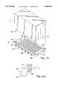
- Another popular prior art packageis the PLCC (Plastic Leaded Chip Carrier) SOJ (Small Outline J-leaded) molded package with twenty surface-mount designed J-leads (length 0.67", width 0.34", height 0.14"). This prior art package is illustrated schematically in FIG. 1 and shown at approximate actual size in FIG. 2.
- SIMMSingle-In-Line Memory Module
- FIGS. 1-3illustrate typical embodiments of some of these prior art packages. Based on experience with those prior art designs, for reasons of reliability related to moisture penetration and mechanical integrity the industry has adopted a standard thickness for plastic packaging of approximately one millimeter (40 mils), or approximately 10.5 mils on each side of a 19 mil thick integrated circuit element.
- the packaging method of the present inventionprovides a reliable, cost efficient, easily manufacturable package with a plurality of ultra thin level-one package elements assembled in an integrated module or level-two package which can be mounted to a printed circuit board directly or via an underlying socket or header.
- the present inventionprovides a level-one packaging method which enables the level-one elements to be packaged in transfer molded casing approximately 7 mils or less thick, encompassing an integrated circuit die element approximately eight to sixteen mils thick to produce a reliable level-one package less than thirty-two mils thick.
- These level-one unitsare then bound together mechanically or using an epoxy adhesive approximately one mil thick, with the outer surfaces of the outside level-one units having a thin metal foil adhered thereto or deposited using known semiconductor manufacturing methods such as vacuum deposition, sputtering or the like.
- This packaging techniqueprovides a high density module or level-two package with improved moisture resistance, and the lamination of multiple level-one elements together provides adequate structural rigidity to prevent intolerable flexing of the internal integrated circuit elements.
- ultra dense reliable packagessuch as the nine megabyte DRAM shown at approximate actual size in FIG. 4 can be achieved.
- the level-one elementsare configured with a single row of leads in either gull-wing or J-lead form for circuit board mounting and interconnect extending from one edge only,and having a heat sink conductive element which comprises a 2 oz. copper foil substrate in full surface contact with the internal integrated circuit die extending from the edge opposite the leads.
- the level-one elementsare laminated together in a vertical array contained within a mounting package which includes metal side plates and a top heat sink element. The vertically extending metal side plates are provided with mounting tangs for attachment to a printed circuit board.
- the level-one unitscan be laminated together at an angle to reduce overall height.
- the packagecan be mounted to a rail header which in turn is mounted to the printed circuit board with J-leads or gull-wing leads for surface mounting. This latter embodiment provides visible solder connections for inspection.
- a horizontally stacked moduleis also provided as an alternative form of the preferred embodiment, which utilizes similar level-one packages laminated together in a horizontal, module or level-two package.
- electrical interconnection and thermal conductionare provided by an array of vertically oriented conductive rails aligned with the vertical columns of leads, and extending from the top to the bottom of the stack. These rails can be configured with SMT gull-wing leads or J-leads for the package.
- Significant advantagesare realized by incorporating an electrical signal bus and integral heat sink in the vertical rails which also provide structural integrity for the horizontal module. In all embodiments provision can be made for decoupling capacitors, control circuitry, self-contained power supplies as elements in the stack and configured with external heat sinking.
- a unique feature of the horizontally oriented level-two module or packageis the relatively large cross-sectional area of the rails connecting the leads of the level-one packages. These rails act as excellent low impedance buses for both electrical current flow and thermal heat transfer.
- the low electrical impedanceprovides for less ground bounce, less signal distortion, and improved signal integrity.
- the low thermal resistanceallows for improved heat transfer from the die interior, which provides increased reliability and longer operating life for some embodiments, and in ultra-high density embodiments provides a package that can be adequately heat compensated with conventional convection techniques.
- FIGS. 1-3illustrate prior art packaging for integrated circuits
- FIG. 4is a schematic illustration of a modular package of the present invention shown at approximate actual size
- FIG. 5illustrates the level-one design of the present invention in schematic cross-section
- FIG. 6illustrates an alternative embodiment of the level-one package of the present invention in schematic cross-section
- FIG. 7illustrates a vertically oriented embodiment of a level-one package according to the present invention in schematic cross-section
- FIG. 8illustrates a horizontal stack embodiment of a level-one package of the present invention having an integral heat sink
- FIG. 9illustrates in schematic cross-section an alternate vertical embodiment of a level-one package according to the present invention.
- FIG. 10illustrates in partial cross-section an alternative embodiment of a level-one package according to the present invention which includes integral heat transfer elements formed in the package casing;
- FIG. 11is an isometric illustration of a vertically oriented level-one package according to the present invention.
- FIGS. 12a, billustrate vertically oriented modular level-two packages according to the present invention
- FIG. 13illustrates an alternative vertically oriented embodiment of a portion of a modular or level-two package according to the present invention
- FIG. 14illustrates an alternative embodiment of a portion of a modular or level-two package according to the present invention
- FIG. 15illustrates a modular level-two vertically oriented package including a plurality of level-one packages and an external heat sink;
- FIG. 15aillustrates assembly details of the package illustrated in FIG. 15;
- FIG. 16illustrates an alternative method and apparatus for assembling a modular, vertically oriented level-two package to a printed circuit board
- FIG. 16aillustrates assembly details for the package shown in FIG. 16
- FIG. 17is an isometric illustration with a partial cut-out view of a horizontally oriented level-one package according to the present invention.
- FIG. 18is an isometric view of a horizontally oriented modular level-two package according to the present invention.
- FIG. 18ais an alternative view of the embodiment illustrated in FIG. 18;
- FIGS. 19a, b, c and dare isometric views of alternative embodiments of conductive rails used in horizontally oriented embodiments illustrated in FIG. 18;
- FIG. 20illustrates an alternative embodiment of a horizontally oriented modular or level-two package according to the present invention
- FIG. 21is a schematic illustration of one method for electrical signal busing of the level-one packages in a modular, level-two package according to the present invention.
- FIG. 22is a schematic illustration of electrical signal busing for a four megabyte by one by nine element DRAM module
- FIG. 23is an isometric view of a alternative embodiment of a level-two package according to the present invention adapted for mounting within an orifice formed in a printed circuit board.
- Package Pcomprises a transfer molded casing 12 surrounding the integrated circuit die 14, which is provided with an array of leads 16 and 18 for circuit interconnection.
- the level-one package Pis formed using conventional, proven manufacturing techniques such as transfer molding and automated tape bonding, or low-profile ribbon or wire bonding to a lead frame, yet achieves substantial reduction in thickness without sacrificing circuit integrity.
- Package Pincludes a silicon integrated circuit die 14 having a nominal thickness of from about eight to about sixteen mils.
- Integrated circuit die 14is provided with an array of conductive leads 16 and 18 for circuit interconnect which are attached to die 14 in the manner described above.
- Leads 16, 18are laid over a semiconductor grade epoxy insulating layer 15 which covers integrated circuit die 14 in a conventional manner. It should also be noted that in some of the drawings leads 16, 18 are illustrated as being connected at or near the edge of integrated circuit die 14 for clarity, whereas in automated bonding the connection pattern is more complex. It should be noted that the present invention is not limited to embodiments having leads exiting at two sides and can be readily fabricated to accommodate single or four sided lead configuration, in either J-lead, gull-wing or other surface mount technology (SMT) lead configurations.
- SMTsurface mount technology
- Integrated circuit die 14is encased in a transfer molded case 12 which may be formed of any suitable commercially available high-temperature semiconductor grade thermosetting plastic such as a filled NOVOLAC material.
- the casing materialshould be selected for high temperature, tolerance, moisture control, mechanical rigidity, and chemical and thermal compatibility with the silicon die 14.
- casing 12is made of a semiconductor grade, low stress, filled, transfer molding compound including a NOVOLAC-type epoxy.
- case 12is formed so as to have a thickness t of approximately five to seven mils.
- a layer of moisture resistant, high glass transition temperature epoxy 20is applied over the upper and lower surfaces of case 12.
- Epoxy 20should be selected to be suitable for curing at approximately 150° C. and endure 250° C. in subsequent manufacturing steps without reflowing.
- Epoxy layer 20is applied in a thickness of one-half to one mil, and is preferably applied in a preformed film or B-stage form.
- a suitable epoxyis an acrylic NOVOLAC-type epoxy with plasticizers.
- the package Pis provided with an outer metal foil layer 22 applied over the B-stage epoxy 20.
- the epoxy layer 20can be applied to foil 22 and both layers applied to the casing at once.
- Foil 22can be aluminum or copper or other suitable metallic foils approximately one-half to one mil thick.
- the completed level-one package Pis therefore approximately forty-five percent to eighty percent of the thickness of prior art packages.
- the epoxy and foil laminationsprevent moisture penetration, and in some applications provide sufficient structural rigidity so as to allow construction of an ultra-thin package while still preventing undesirable flexing of the integrated circuit die 14. Protection against moisture penetration is achieved because moisture can only penetrate from lead edges 24 and 26 and the distance t 2 from edges 24 and 26 to integrated circuit die 14 is greater than twenty-five mils.
- package Pincludes a integrated circuit die 14 surrounded by a transfer molded casing 12 of the type previously described.
- Leads 16 and 18are tape or ribbon bonded to integrated circuit die 14 in the conventional manner.
- This embodimentdoes not include an epoxy layer 20 as in the previous embodiment, but instead only includes a thin (one-half to ten microns thick) metal foil lamination 22 formed of aluminum or copper foil adhered, vacuum deposited, or otherwise applied on surfaces 23 and 25 of casing 12.
- Embodiment P 2is configured to have an integral full-surface contact conductive heat sink element 30 mounted to one surface of integrated circuit die 14.
- Element 30is formed of aluminum or copper 1.4 mil to 2.8 mil thick which is surface-mounted to integrated circuit die 14 using a semiconductor grade, metal-filled heat conductive epoxy layer 15.
- Element 30extends from one end 32 of package P 2 and is bent to form a heat sink end 34 shaped to dissipate heat by convection or To be attached to a larger heat sink element (not shown).
- end 34 of heat sink 30, as well as other lead type extensions from the level-one packagesshould be formed of flexible material and extend far enough from the package to avoid unduly stressing the package or the die connection when the package is mounted to external electrical or mechanical supports. Extension of seven to eight mils in addition to any connection length required is sufficient for these purposes.
- all leads 38extend from edge 36 of package P 2 . While in FIG. 7 package P 2 includes a transfer molded casing 12, an epoxy lamination layer 20 and foil lamination layers 22 as in the previous embodiment shown in FIG. 5, this integral heat sink embodiment could be just as readily formed without epoxy layer 20 as illustrated in FIG. 6.
- a horizontal stack embodiment P 3is illustrated in schematic isometric form.
- leads 16 and 18extend from sides 44 and 46 and are attached to integrated circuit die 14 (not shown) in the manner described above.
- Heat sink element 30is surfaced mounted to integrated circuit die 14 in the manner described above with reference to FIG. 7, and brought out of end 48 of package P 3 for independent heat dissipation or for attachment to a larger heat sink element.
- heat transfercan be achieved without element 30.
- heatis transferred from integrated circuit die 14 through casing 12, epoxy layer 20 and foil layer 22 (FIGS. 5 and 6).
- FIG. 9Yet another alternative, level-one embodiment is illustrated in FIG. 9.
- all circuit leads 52extend from end 54 of package P 4 .
- Package P 4includes casing 12, integrated circuit die 14, and optional epoxy layer 20 as in previous embodiments.
- foil layers 56 and 58wrap around end 60 of package P 4 and are joined together to form a heat sink element similar to element 30 of FIG. 7.
- Foil layers 56 and 58are epoxy-bonded to package P 4 and to each other at end 62 using a one-half mil epoxy layer of the type previously described.
- package P 5includes a integrated circuit die 14, case 12, optional epoxy upper layer 20 and foil layers 22 as previously described.
- cavities 66are formed in case 12 and filled with thermally conductive epoxy material 68.
- an epoxy adhesive layer 70is formed about one-half mil thick to which foil layer 22 is adhered.
- heat sink element 30is formed as a conductive sheet, surface mounted to integrated circuit die 14 via a layer of metal-filled, semiconductor grade heat transfer epoxy 72.
- Element 30is formed having a plurality of slots 74 cut from element 30 prior to fabrication of package P 2 . While not shown in precise scale, slots 74 are formed so as to relieve stress in transfer molding casing 12. In this manner, casing 12 is formed around leads 38 and through slots 74 of heat sink element 30.
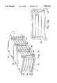
- Another aspect of the present inventionrelates to the manner in which level-one packages, in either vertical or horizontal configuration can be assembled into a multi-element, modular level-two package or stack for mounting to an underlying printed circuit board.
- FIG. 12aa level-two package M is formed of a plurality of vertically oriented level-one packages P 2 and mounted to an underlying printed circuit board 800. The details of the assembly and mounting of package M are described below.
- FIG. 12bAn alternate embodiment which reduces the overall height of package M is illustrated in FIG. 12b.
- package M and the constituent level-one packages P 2are inclined at an angle to reduce overall package height.
- package Mincludes a metal or otherwise heat conductive and electrically insulated outer casing 82 formed of a continuous sheet of metal approximately six mils thick.
- FIG. 13an alternate embodiment of a portion of a vertical stack assembly of package M is illustrated.
- a plurality of level-one packages P 2are assembled by applying epoxy bond 80 between each element P 2 .
- Each element P 2includes a integrated circuit die 14, a case 12, lead elements 38 and heat sink elements 30 as previously described.
- each element P 2is individually manufactured and tested without applying exterior epoxy layer 20 or foil layer 22 (FIG. 7). Thereafter, on a first element P 2-1 (FIG. 13) an epoxy layer 82, similar to layer 20 described above, is applied to one surface of a conductive foil layer 86, and the combined lamination of layers 82 and 86 is adhered to surface 84. After testing element P 2-1 , a second layer of epoxy 80 is applied to the second, opposite side of element P 2-1 , and a second level-one package P 2-2 is attached to package P 2-1 . Thereafter, the combined element formed of packages P 2-1 and P 2-2 is tested. Further elements P 2-3 , through P 2-7 , for example, are similarly assembled.
- the last element P 2-Nis adhered to the preceding element in the same manner.
- An epoxy layer 80 and a conductive foil layer 86is then applied to the outside surface 88 of the last element P 2-N to complete the assembly.
- the assembled level-two unit M 1(FIG. 13) thereby includes a number of level-one elements bonded together in laminated fashion, having conductive foil layers applied to the exterior flat surfaces of the outside elements in the stack. This lamination provides improved resistance to moisture penetration and enhances the structural rigidity of the package as a whole enabling thinner individual circuit elements P 2 to be used without sacrificing circuit integrity.
- each element P 2is provided with only exterior foil layers 22.
- the individual packages P 2are mechanically bound together with any suitable means such as a tie 87 or a housing 82 as shown in FIGS. 12a or 15 surrounding the package M 2 .
- Assembled stacks M 1 or M 2may be mounted in an exterior package V as illustrated in FIG. 15.
- Package Vincludes an exterior casing 90 which is a metal formed shield which may be in two pieces (FIG. 15) or may be a single piece traversing over the top of stack M 1 (numeral 82, FIG. 12a).
- Casing 90is formed of sheet metal approximately six mils thick.
- Casing 90also includes at each of the four corners of package V a printed circuit board mounting tab or locating pin 94 having an expanded portion midway on its length to form a height setting tab 96 to position package V above an underlying printed circuit board or header as described below.
- the individual level-one elements P 2are either epoxy bonded together with a one mil thick epoxy layer 81 or mechanically bound together as previously described.
- Stack M 1 or M 2may be adhered to casing 90 with an approximately one mil thick epoxy bond between outside surfaces of the stack M 1 or M 2 and interior surfaces of casing 90, or mechanically attached using any suitable clamping method.
- Package Valso includes a u-shaped heat sink element 100 formed of heat conductive material and shaped to fit snugly over the assembled stack M 1 and casing 90 so as to form an upper cap for package V.
- heat sink 100When affixed to package V heat sink 100 provides structural rigidity as well as heat transfer capability.
- Heat sink 100is bonded to level-one heat sink elements 30 (FIG. 15a) via conductive epoxy bond 102.
- elements 30 of each element P 2Prior to assembly, elements 30 of each element P 2 are uniformly bent to provide a relatively coplanar bonding surface for heat sink 100.
- the under surface 104 of heat sink 100is coated with B-stage conductive epoxy and pushed onto the partially assembled package V so that surface 104 contacts each of the P 2 heat sink elements 30. Thereafter heat is applied to complete the bond 102.
- package Vis mounted to a preformed plastic non-conductive header H which is subsequently mounted to a printed circuit board to provide socket-type mounting.
- package Vis mounted to header H via mounting tabs 94 which fit into preformed holes 110 in header H.
- Header Hincludes a rectangular frame 114 provided with a number of J-lead or gull-wing configured leads 112 which span the width of frame 114 and are uniformly spaced along two opposite sides of the perimeter of frame 114 consistent with industry standard spacing.
- Frame 114is formed of high temperature plastic or transfer molding compound such as RYTON.
- Leads 112extend from the perimeter of frame 114 as shown in detail in FIG. 16a. Leads 112 may be formed in conventional J-lead, gull-wing or other surface mount configuration as required.
- alternating leads 112a(FIG. 16) are configured to have the J-lead or terminal portion 116 on the opposite side of frame 114 as leads 112, with the non-terminal ends being flush with the exterior surface 118 of frame 114.
- Leads 112, 112aare formed of approximately five-mil copper having a rectangular cross-section. Leads 112, 112a are mounted in frame 114 through preformed rectangular slots 120. The portion of leads 112, 112a within slots 120 are horizontally configured, and the portion within the interior of frame 114 are rotated or twisted ninety degrees to be vertically oriented (FIG. 16a). To facilitate mounting package V, leads 112, 112a are plated or solder-coated for subsequent attachment to individual leads 38 which are pre-treated with solder paste just prior to assembly.
- stack Vis mounted to header H by insertion of tabs 94 into holes 110. Tabs 94 are then bent or glued to header H to temporarily hold stack V in place while leads 38 are soldered to leads 112, 112a. This configuration provides socket mounting and visible solder connections for serviceability.
- FIG. 17the preferred embodiment of a horizontally oriented level-one package suitable for modular or level-two assembly is illustrated with a partial cut-out view of some interior details.
- the horizontal level-one packageis preferred where overall height is a key consideration.
- the level-one package Pis constructed essentially as described above with reference to FIGS. 5 and 6 but may also include the integral heat sink element as shown in FIG. 8.
- Package Pis formed with a casing 12, optional epoxy layer 20 and aluminum foil layer 22 laminated above and below an integrated circuit die 14 (FIGS. 5-6).
- the cut-out (FIG. 18)shows typical interior details of such a package wherein leads 16 and 18 extend laterally from package P, and are bent downward at an angle less than ninety degrees to provide spring-loading which facilitates mounting as described below.
- Leads 16 and 18are formed of copper approximately one and four-tenths to two and eight-tenths mils thick in a substantially rectangular cross-section and with adequate temper to provide a relatively flat, flexible connector.
- Leads 16 and 18are bonded over integrated circuit die 14 with a two-mil semiconductor grade adhesive dielectric 130 using conventional automated tape bonding or low-profile ribbon or wire bonding techniques to a copper lead frame 131 to bond the leads to bonding pads 132 at the perimeter of die 14.
- Leads 16, 18are extended from package P and bent at their distal ends to provide flexibility for stress relief in mounting as described above.
- each package Pis formed having a nesting slot or detent 136 at each of four corners, such slots 136 being formed to receive a complimentary shaped nesting tab 138 formed at the lower surface at each of the four corners.
- the individual level-one packages Pare assembled in a horizontally oriented level-two package T in the manner illustrated in FIG. 18. Each package P is individually assembled and tested prior to assembly in horizontal stack package T.
- Package Tis built upon a hard-anodized aluminum base 142 which alternatively can be formed of molded RYTON, or other suitable electrically insulating material. While FIG. 18 illustrates an assembly of four level-one packages for clarity, it should be noted that the typical package T would include eight or nine level-one packages. Furthermore, while some of the drawings illustrate a package P having only four leads 16, 18 per side for clarity, a typical package P would include many more (typically 28), depending upon the pin-out requirements of the particular integrated circuit being packaged.
- Level-one packages P for assembly into multiple-unit level-two packages Tare formed as described above.
- Each unit Pincludes a integrated circuit die 14, a case 12 a metallic foil lamination 22 and may include epoxy lamination layer 20 (FIGS. 5, 6).
- the individual packages Pare simply mechanically bound together by the structural members of package T (FIG. 18).
- each level-one package Pcan be adhered to the package P immediately above and below with a one-mil thick epoxy adhesive 148, and only upper and lower level-one packages P 10 and P 11 are provided with a metal foil lamination 146 over an adhesive layer 148 at the upper and lower surfaces of P 10 and P 11 , respectively.
- each of leads 16, 18(FIG. 17) is formed of copper to provide spring-like resiliency, and extended from package P to allow stress relief.
- package Tincludes base 142, level-one packages P stacked above base 142, electrically and thermally conductive external rails 150 electrically and thermally coupled to leads 16 and 18, and a cap member 160.
- Cap member 160 and base member 142must be electrically isolated from rails 150 and preferably should be formed of thermally conductive material.
- non-conducting plasticssuch as RYTON
- cap 160 and base 142can be formed of heat conductive materials such as plastic coated aluminum or preferably hard-anodized aluminum without coating.
- Cap 160includes a plurality of slots 161 formed to be aligned with upper portions 162 of rails 150. Once the stack of packages P are assembled, cap 160 is adhered to the upper surface of package P 10 , with upper portions 162 of rails 150 extending through slots 161 and being bent over to clamp rails 150 to cap 160.
- Rails 150include a lower portion 152 (FIG. 19) which further includes base mounting tab 155 and a circuit board mounting portion 154 configured in either J-lead or gull-wing configuration (FIGS. 19a, b). Additionally, rails 150 can include an integral heat sink flange 157 (FIG. 19d) for improved heat dissipation.
- Assembly of level-two package Tcan be in one of two formats.
- first formatall of the required level-one packages P are horizontally stacked above base 142 and adhered or bound to one another first, and thereafter assembly continues with the provision of a plurality of vertically oriented lead rail elements 150.
- Rail elements 150are formed of conductive resilient material such as 110 alloy copper having a cross-sectional thickness in the range of four to eight-mils.
- Each rail element(FIG. 19) comprises an intermediate lead contact portion 152 and a lower J-lead, butt-lead or gull-wing configured SMT contact portion 154.
- assembly and testingare conducted level by level, with each level-one package P being assembled, tested, mounted on the stack, with leads 16, 18 soldered to the corresponding rails 150, and re-tested before a subsequent level-one package P is added to the stack.
- This methodologyinsures that all level-one elements are functional before subsequent elements are added to the stack to avoid waste.
- level-one packagesare to be mounted in the stack without adhesive bonding between level-one elements, the following procedure is utilized:
- Assembleincluding integrated circuit burn-in and fully test a plurality of level-one packages, sorting level-one packages by speed or signal response time to ensure speed uniformity in level-two modules;
- Assembleincluding integrated circuit burn-in and fully test a plurality of level-one packages, sorting level-one packages by speed or signal response time to ensure speed uniformity in level-two modules;
- Cap 160is formed having a plurality of slots 161 to receive the upper ends 162 (FIG. 19a) of rails 150.
- heat sinksmay be attached to the package T in one of several alternative embodiments.
- heat sink elements 170are mounted to the exterior surface of portions 152 of rails 150 by means providing for electrical insulation but thermal conductance.
- One methodis to bond heat sinks 170 to rails 150 using a two-mil thick high temperature epoxy adhesive.
- a two-mil thick beryllium oxide padcan be interposed between heat sinks 170 and rails 150 and adhered to sinks 170 and rails 150 with a suitable high temperature adhesive.
- Such heat sinksare preferably formed of anodized aluminum.
- heatis dissipated via the rails 150 without additional external heat sinks, or via integral heat sink flanges providing increased surface area for rails 150 such as the embodiment shown in FIG. 19d.
- Assembleincluding integrated circuit burn-in and fully test a plurality of level-one packages, sorting level-one packages by speed or signal response time to ensure speed uniformity in level-two modules;
- header assemblyinto a temporary fixture and assemble all level-one packages into the rail/header assembly
- heatis conducted from the level-one packages P via leads 16, 18 to rails 150 and thereafter dissipated in heat sinks 170.
- a horizontal level-one package with integral heat sink elements 30is employed (FIG. 8)
- an additional set of rails 150 on a third side of package Tare soldered to elements 30 in the same manner as described above, and an additional heat sink 170 can be attached.
- each of rails 150are formed including an upper, horizontally oriented extension 180 which extends through cap 160 and traverses slightly less than half way across the width of cap 160 so as to be in surface contact with the upper surface of cap 160.
- An additional heat sink 182is affixed to extensions 180 of rails 150 using a heat conductive adhesive. In this manner, heat from level-one packages P is conducted through leads 16 and 18 to rails 150 and dissipated in heat sinks 170 and 182.
- a major advantage of the inventionis in the resulting efficiency and flexibility for thermal management of the module.
- a nine-high modulefour megabytes by one by nine
- a ⁇ JCof less than 20° C./watt is desirable.
- the various embodiments of the level-one packages of the present inventionprovide an extremely efficient 2° C. to 5° C./watt ⁇ JC, and the modular package may be designed to provide a 15° C. to 20° C./watt ⁇ JC. This design thus permits the utilization of conventional air-cooling convection and conduction through the leads 16, 18 to rails 150 and heat sinks or a combination of these methods, as distinguished from more complicated and expensive cooling techniques.
- the level-two modular constructionis especially useful to provide a multiple element memory array.
- An example of this arraywould be a four megabyte by one by nine array to form a four megabit plus parity DRAM module.
- This modulewould be a single package replacement for a four megabyte plus parity SIMM card.
- Each individual element P of the modulewill have twenty-eight leads where only eighteen of the twenty-eight leads require connection to the bus rails 150. The leads not requiring a connection for each element P are severed from the device flush to the package P.
- the tape lead framewhich provides the internal, level-one die to lead connections, provides for a common data-in, data-out bus. This bus will connect to eight pins on the package.
- Static ramscould be packaged in a four high module to provide either a four, sixteen, or thirty-two bit wide array.
- DRAMScould also be packaged in four or five high stacks to accommodate those areas where product height is a concern.
- the five-high stackcould be settled as a standard height, with a common header for the stack. For the four-high stack a "dummy" spacer layer will be added to maintain the product standard size.
- FIG. 21provides an exemplary four megabyte plus parity DRAM configuration. The following table represents examples of configurations, pin counts, data widths and product types:
- the foregoing descriptionprovides details of preferred embodiments of an ultra-thin level-one integrated circuit package and a method of assembling level-one packages into a high density level-two package.
- the laminated structure of the level-one packagesprovides moisture protection and structural resistance to flexing to enable an ultra-thin package to be constructed without loss of circuit integrity.
- the level-two packageprovides high density and thermal and environmental control in an easily manufactured package.
Landscapes
- Engineering & Computer Science (AREA)
- Microelectronics & Electronic Packaging (AREA)
- Power Engineering (AREA)
- Physics & Mathematics (AREA)
- Condensed Matter Physics & Semiconductors (AREA)
- General Physics & Mathematics (AREA)
- Computer Hardware Design (AREA)
- Manufacturing & Machinery (AREA)
- Cooling Or The Like Of Semiconductors Or Solid State Devices (AREA)
- Lead Frames For Integrated Circuits (AREA)
Abstract
Description
__________________________________________________________________________ Total Pin Output Word Product Chip Memory Configuration Count Length __________________________________________________________________________DRAM 1 Meg 9M Bit 1M × 1 × 9 26 8 B, +1 Par. DRAM 1 Meg 9M Bit 256K × 4 × 9 52 32 B, +4 Par. DRAM 4 Meg 36M Bit 1M × 4 × 9 53 32 B, +4 Par. DRAM 4 Meg 36M Bit 4M × 1 × 9 28 8 B, +1 Par. SRAM 256K 2M Bit 256K × 1 × 8 30 8 B SRAM 256K 1M Bit 256K × 1 × 4 26 4 B SRAM 256K 2M Bit 64K × 4 × 8 52 32 B SRAM 256K 1M Bit 64K × 4 × 8 36 16 B SRAM 1 Meg 8M Bit 256K × 4 × 8 55 32 B SRAM 1 Meg 4M Bit 256K × 4 × 4 39 16 B __________________________________________________________________________ For those (× 1) memory chips with separate Din, Dout lines, the Din and Dout lines are tied together. The parity Din and Dout are not tied together.
Claims (17)
Priority Applications (1)
| Application Number | Priority Date | Filing Date | Title |
|---|---|---|---|
| US08/298,544US5566051A (en) | 1990-08-01 | 1994-08-30 | Ultra high density integrated circuit packages method and apparatus |
Applications Claiming Priority (2)
| Application Number | Priority Date | Filing Date | Title |
|---|---|---|---|
| US56141790A | 1990-08-01 | 1990-08-01 | |
| US08/298,544US5566051A (en) | 1990-08-01 | 1994-08-30 | Ultra high density integrated circuit packages method and apparatus |
Related Parent Applications (1)
| Application Number | Title | Priority Date | Filing Date |
|---|---|---|---|
| US56141790AContinuation | 1990-08-01 | 1990-08-01 |
Publications (1)
| Publication Number | Publication Date |
|---|---|
| US5566051Atrue US5566051A (en) | 1996-10-15 |
Family
ID=24241892
Family Applications (5)
| Application Number | Title | Priority Date | Filing Date |
|---|---|---|---|
| US08/059,401Expired - Fee RelatedUS5279029A (en) | 1990-08-01 | 1993-05-11 | Ultra high density integrated circuit packages method |
| US08/133,397Expired - LifetimeUS5420751A (en) | 1990-08-01 | 1993-10-08 | Ultra high density modular integrated circuit package |
| US08/289,468Expired - LifetimeUS5561591A (en) | 1990-08-01 | 1994-08-12 | Multi-signal rail assembly with impedance control for a three-dimensional high density integrated circuit package |
| US08/298,544Expired - LifetimeUS5566051A (en) | 1990-08-01 | 1994-08-30 | Ultra high density integrated circuit packages method and apparatus |
| US08/375,747Expired - Fee RelatedUS5543664A (en) | 1990-08-01 | 1995-01-20 | Ultra high density integrated circuit package |
Family Applications Before (3)
| Application Number | Title | Priority Date | Filing Date |
|---|---|---|---|
| US08/059,401Expired - Fee RelatedUS5279029A (en) | 1990-08-01 | 1993-05-11 | Ultra high density integrated circuit packages method |
| US08/133,397Expired - LifetimeUS5420751A (en) | 1990-08-01 | 1993-10-08 | Ultra high density modular integrated circuit package |
| US08/289,468Expired - LifetimeUS5561591A (en) | 1990-08-01 | 1994-08-12 | Multi-signal rail assembly with impedance control for a three-dimensional high density integrated circuit package |
Family Applications After (1)
| Application Number | Title | Priority Date | Filing Date |
|---|---|---|---|
| US08/375,747Expired - Fee RelatedUS5543664A (en) | 1990-08-01 | 1995-01-20 | Ultra high density integrated circuit package |
Country Status (4)
| Country | Link |
|---|---|
| US (5) | US5279029A (en) |
| EP (1) | EP0509065A1 (en) |
| AU (1) | AU8519891A (en) |
| WO (1) | WO1992003035A1 (en) |
Cited By (57)
| Publication number | Priority date | Publication date | Assignee | Title |
|---|---|---|---|---|
| US5837566A (en)* | 1994-06-23 | 1998-11-17 | Cubic Memory, Inc. | Vertical interconnect process for silicon segments |
| US5891761A (en)* | 1994-06-23 | 1999-04-06 | Cubic Memory, Inc. | Method for forming vertical interconnect process for silicon segments with thermally conductive epoxy preform |
| US5956236A (en)* | 1997-11-25 | 1999-09-21 | Micron Technology, Inc. | Integrated circuit package support system |
| US5978224A (en)* | 1997-12-04 | 1999-11-02 | Intel Corporation | Quad flat pack integrated circuit package |
| US5994170A (en)* | 1994-06-23 | 1999-11-30 | Cubic Memory, Inc. | Silicon segment programming method |
| US6025642A (en)* | 1995-08-17 | 2000-02-15 | Staktek Corporation | Ultra high density integrated circuit packages |
| US6049123A (en)* | 1990-08-01 | 2000-04-11 | Staktek Corporation | Ultra high density integrated circuit packages |
| US6075288A (en)* | 1998-06-08 | 2000-06-13 | Micron Technology, Inc. | Semiconductor package having interlocking heat sinks and method of fabrication |
| US6080596A (en)* | 1994-06-23 | 2000-06-27 | Cubic Memory Inc. | Method for forming vertical interconnect process for silicon segments with dielectric isolation |
| US6124633A (en)* | 1994-06-23 | 2000-09-26 | Cubic Memory | Vertical interconnect process for silicon segments with thermally conductive epoxy preform |
| USRE36916E (en)* | 1995-03-21 | 2000-10-17 | Simple Technology Incorporated | Apparatus for stacking semiconductor chips |
| US6144107A (en)* | 1998-03-26 | 2000-11-07 | Nec Corporation | Solid state pickup device excellent in heat-resistance and method of manufacturing the device |
| US6242285B1 (en) | 1998-07-23 | 2001-06-05 | Kyung Suk Kang | Stacked package of semiconductor package units via direct connection between leads and stacking method therefor |
| US6255726B1 (en) | 1994-06-23 | 2001-07-03 | Cubic Memory, Inc. | Vertical interconnect process for silicon segments with dielectric isolation |
| US6326687B1 (en)* | 1998-09-01 | 2001-12-04 | Micron Technology, Inc. | IC package with dual heat spreaders |
| US20020009828A1 (en)* | 1996-06-28 | 2002-01-24 | Pac Tech - Packaging Technologies Gmbh | Process for the formation of a spatial chip arrangement and spatial chip arrangement |
| US20020017709A1 (en)* | 2000-06-07 | 2002-02-14 | Yoshiyuki Yanagisawa | Assembly jig and manufacturing method of multilayer semiconductor device |
| US6446316B1 (en)* | 1994-05-02 | 2002-09-10 | Siemens Matsushita Components Gmbh & Co. Kg | Method for producing an encapsulation for a SAW component operating with surface acoustic waves |
| US6462408B1 (en) | 2001-03-27 | 2002-10-08 | Staktek Group, L.P. | Contact member stacking system and method |
| US6486528B1 (en) | 1994-06-23 | 2002-11-26 | Vertical Circuits, Inc. | Silicon segment programming apparatus and three terminal fuse configuration |
| US20030090008A1 (en)* | 1998-10-01 | 2003-05-15 | Micron Technology, Inc. | Integrated circuit device |
| US6572387B2 (en) | 1999-09-24 | 2003-06-03 | Staktek Group, L.P. | Flexible circuit connector for stacked chip module |
| US6576992B1 (en) | 2001-10-26 | 2003-06-10 | Staktek Group L.P. | Chip scale stacking system and method |
| US6608763B1 (en) | 2000-09-15 | 2003-08-19 | Staktek Group L.P. | Stacking system and method |
| US6731011B2 (en) | 2002-02-19 | 2004-05-04 | Matrix Semiconductor, Inc. | Memory module having interconnected and stacked integrated circuits |
| US20040168316A1 (en)* | 1998-08-21 | 2004-09-02 | Moden Walter L. | Low profile multi-IC chip package connector |
| US20040178496A1 (en)* | 2001-10-26 | 2004-09-16 | Staktek Grop, L.P. | Memory expansion and chip scale stacking system and method |
| US20040183183A1 (en)* | 2001-10-26 | 2004-09-23 | Staktek Group, L.P. | Integrated circuit stacking system and method |
| US20040191442A1 (en)* | 2003-03-27 | 2004-09-30 | Florencia Lim | Surface modification of expanded ultra high molecular weight polyethylene (eUHMWPE) for improved bondability |
| US6867486B2 (en) | 2001-08-30 | 2005-03-15 | Hynix Semiconductor Inc. | Stack chip module with electrical connection and adhesion of chips through a bump for improved heat release capacity |
| US6919626B2 (en) | 1992-12-11 | 2005-07-19 | Staktek Group L.P. | High density integrated circuit module |
| US6940729B2 (en) | 2001-10-26 | 2005-09-06 | Staktek Group L.P. | Integrated circuit stacking system and method |
| US20050224952A1 (en)* | 2004-04-13 | 2005-10-13 | Al Vindasius | Three dimensional six surface conformal die coating |
| US20050258530A1 (en)* | 2004-04-13 | 2005-11-24 | Al Vindasius | Micropede stacked die component assembly |
| US6995412B2 (en) | 2002-04-12 | 2006-02-07 | International Business Machines Corporation | Integrated circuit with capacitors having a fin structure |
| US7033861B1 (en) | 2005-05-18 | 2006-04-25 | Staktek Group L.P. | Stacked module systems and method |
| US7053478B2 (en) | 2001-10-26 | 2006-05-30 | Staktek Group L.P. | Pitch change and chip scale stacking system |
| US7094632B2 (en) | 2001-10-26 | 2006-08-22 | Staktek Group L.P. | Low profile chip scale stacking system and method |
| US7126218B1 (en)* | 2001-08-07 | 2006-10-24 | Amkor Technology, Inc. | Embedded heat spreader ball grid array |
| US7180167B2 (en) | 2001-10-26 | 2007-02-20 | Staktek Group L. P. | Low profile stacking system and method |
| US7193310B2 (en) | 2001-12-14 | 2007-03-20 | Stuktek Group L.P. | Stacking system and method |
| US7202555B2 (en) | 2001-10-26 | 2007-04-10 | Staktek Group L.P. | Pitch change and chip scale stacking system and method |
| US20070091574A1 (en)* | 2005-10-26 | 2007-04-26 | Indium Corporation Of America | Technique for forming a thermally conductive interface with patterned metal foil |
| US7215018B2 (en) | 2004-04-13 | 2007-05-08 | Vertical Circuits, Inc. | Stacked die BGA or LGA component assembly |
| US7304382B2 (en) | 2006-01-11 | 2007-12-04 | Staktek Group L.P. | Managed memory component |
| US7309914B2 (en) | 2005-01-20 | 2007-12-18 | Staktek Group L.P. | Inverted CSP stacking system and method |
| US7371609B2 (en) | 2001-10-26 | 2008-05-13 | Staktek Group L.P. | Stacked module systems and methods |
| US7468553B2 (en) | 2006-10-20 | 2008-12-23 | Entorian Technologies, Lp | Stackable micropackages and stacked modules |
| US7485951B2 (en) | 2001-10-26 | 2009-02-03 | Entorian Technologies, Lp | Modularized die stacking system and method |
| US7508069B2 (en) | 2006-01-11 | 2009-03-24 | Entorian Technologies, Lp | Managed memory component |
| US7508058B2 (en) | 2006-01-11 | 2009-03-24 | Entorian Technologies, Lp | Stacked integrated circuit module |
| US7542304B2 (en) | 2003-09-15 | 2009-06-02 | Entorian Technologies, Lp | Memory expansion and integrated circuit stacking system and method |
| US7576995B2 (en) | 2005-11-04 | 2009-08-18 | Entorian Technologies, Lp | Flex circuit apparatus and method for adding capacitance while conserving circuit board surface area |
| US7605454B2 (en) | 2006-01-11 | 2009-10-20 | Entorian Technologies, Lp | Memory card and method for devising |
| US7608920B2 (en) | 2006-01-11 | 2009-10-27 | Entorian Technologies, Lp | Memory card and method for devising |
| US7656678B2 (en) | 2001-10-26 | 2010-02-02 | Entorian Technologies, Lp | Stacked module systems |
| US20100078200A1 (en)* | 2008-09-30 | 2010-04-01 | Jr-Yi Shen | Flex circuit assembly with a dummy trace between two signal traces |
Families Citing this family (263)
| Publication number | Priority date | Publication date | Assignee | Title |
|---|---|---|---|---|
| US20010030370A1 (en)* | 1990-09-24 | 2001-10-18 | Khandros Igor Y. | Microelectronic assembly having encapsulated wire bonding leads |
| US5148265A (en) | 1990-09-24 | 1992-09-15 | Ist Associates, Inc. | Semiconductor chip assemblies with fan-in leads |
| US7198969B1 (en) | 1990-09-24 | 2007-04-03 | Tessera, Inc. | Semiconductor chip assemblies, methods of making same and components for same |
| US5155067A (en)* | 1991-03-26 | 1992-10-13 | Micron Technology, Inc. | Packaging for a semiconductor die |
| US5383269A (en)* | 1991-09-03 | 1995-01-24 | Microelectronics And Computer Technology Corporation | Method of making three dimensional integrated circuit interconnect module |
| FR2688630B1 (en)* | 1992-03-13 | 2001-08-10 | Thomson Csf | METHOD AND DEVICE FOR THREE-DIMENSIONAL INTERCONNECTION OF ELECTRONIC COMPONENT PACKAGES. |
| US5247423A (en)* | 1992-05-26 | 1993-09-21 | Motorola, Inc. | Stacking three dimensional leadless multi-chip module and method for making the same |
| US5371866A (en)* | 1992-06-01 | 1994-12-06 | Staktek Corporation | Simulcast standard multichip memory addressing system |
| EP0586888B1 (en)* | 1992-08-05 | 2001-07-18 | Fujitsu Limited | Three-dimensional multichip module |
| US5544017A (en)* | 1992-08-05 | 1996-08-06 | Fujitsu Limited | Multichip module substrate |
| KR940008054A (en)* | 1992-09-01 | 1994-04-28 | 김광호 | Structure of Semiconductor Package |
| FR2696871B1 (en)* | 1992-10-13 | 1994-11-18 | Thomson Csf | Method of 3D interconnection of housings of electronic components, and 3D components resulting therefrom. |
| US5484959A (en)* | 1992-12-11 | 1996-01-16 | Staktek Corporation | High density lead-on-package fabrication method and apparatus |
| US5541812A (en)* | 1995-05-22 | 1996-07-30 | Burns; Carmen D. | Bus communication system for stacked high density integrated circuit packages having an intermediate lead frame |
| US5455740A (en)* | 1994-03-07 | 1995-10-03 | Staktek Corporation | Bus communication system for stacked high density integrated circuit packages |
| US5369056A (en)* | 1993-03-29 | 1994-11-29 | Staktek Corporation | Warp-resistent ultra-thin integrated circuit package fabrication method |
| CA2118994A1 (en)* | 1993-06-21 | 1994-12-22 | Claude L. Bertin | Polyimide-insulated cube package of stacked semiconductor device chips |
| US5362986A (en)* | 1993-08-19 | 1994-11-08 | International Business Machines Corporation | Vertical chip mount memory package with packaging substrate and memory chip pairs |
| US5905300A (en)* | 1994-03-31 | 1999-05-18 | Vlsi Technology, Inc. | Reinforced leadframe to substrate attachment |
| US5619067A (en)* | 1994-05-02 | 1997-04-08 | Texas Instruments Incorporated | Semiconductor device package side-by-side stacking and mounting system |
| AU2371795A (en)* | 1994-05-17 | 1995-12-05 | Olin Corporation | Electronic packages with improved electrical performance |
| US5567654A (en)* | 1994-09-28 | 1996-10-22 | International Business Machines Corporation | Method and workpiece for connecting a thin layer to a monolithic electronic module's surface and associated module packaging |
| US5545942A (en)* | 1994-11-21 | 1996-08-13 | General Electric Company | Method and apparatus for dissipating heat from a transducer element array of an ultrasound probe |
| US5466634A (en)* | 1994-12-20 | 1995-11-14 | International Business Machines Corporation | Electronic modules with interconnected surface metallization layers and fabrication methods therefore |
| US5588205A (en)* | 1995-01-24 | 1996-12-31 | Staktek Corporation | Method of manufacturing a high density integrated circuit module having complex electrical interconnect rails |
| US5592364A (en)* | 1995-01-24 | 1997-01-07 | Staktek Corporation | High density integrated circuit module with complex electrical interconnect rails |
| US5615475A (en)* | 1995-01-30 | 1997-04-01 | Staktek Corporation | Method of manufacturing an integrated package having a pair of die on a common lead frame |
| GB9507360D0 (en)* | 1995-04-08 | 1995-05-31 | Hybrid Memory Products Limited | Integrated circuit packages |
| DE69609921T2 (en)* | 1995-05-12 | 2001-03-15 | Koninklijke Philips Electronics N.V., Eindhoven | MANUFACTURING METHOD OF A SEMICONDUCTOR ARRANGEMENT SUITABLE FOR SURFACE MOUNTING |
| US5657537A (en)* | 1995-05-30 | 1997-08-19 | General Electric Company | Method for fabricating a stack of two dimensional circuit modules |
| US5661901A (en)* | 1995-07-10 | 1997-09-02 | Micron Technology, Inc. | Method for mounting and electrically interconnecting semiconductor dice |
| US5861666A (en)* | 1995-08-30 | 1999-01-19 | Tessera, Inc. | Stacked chip assembly |
| US5754405A (en)* | 1995-11-20 | 1998-05-19 | Mitsubishi Semiconductor America, Inc. | Stacked dual in-line package assembly |
| US5754408A (en)* | 1995-11-29 | 1998-05-19 | Mitsubishi Semiconductor America, Inc. | Stackable double-density integrated circuit assemblies |
| US5623395A (en)* | 1995-12-15 | 1997-04-22 | Mitsubishi Semiconductor America, Inc. | Integrated circuit package assembly |
| US5790381A (en)* | 1995-12-15 | 1998-08-04 | Mitsubishi Semiconductor America, Inc. | Integrated circuit package assembly |
| US5807762A (en)* | 1996-03-12 | 1998-09-15 | Micron Technology, Inc. | Multi-chip module system and method of fabrication |
| US5778522A (en)* | 1996-05-20 | 1998-07-14 | Staktek Corporation | Method of manufacturing a high density integrated circuit module with complex electrical interconnect rails having electrical interconnect strain relief |
| US5892660A (en) | 1996-08-29 | 1999-04-06 | Micron Technology, Inc. | Single in line memory module adapter |
| US5747858A (en)* | 1996-09-30 | 1998-05-05 | Motorola, Inc. | Electronic component having an interconnect substrate adjacent to a side surface of a device substrate |
| US5860210A (en)* | 1996-09-30 | 1999-01-19 | Motorola, Inc. | Method of manufacturing an electronic component |
| JP3398004B2 (en)* | 1997-03-24 | 2003-04-21 | ローム株式会社 | Package type semiconductor device structure |
| US6028352A (en)* | 1997-06-13 | 2000-02-22 | Irvine Sensors Corporation | IC stack utilizing secondary leadframes |
| US6163459A (en)* | 1997-07-25 | 2000-12-19 | Matsushita Electric Industrial Co., Ltd. | Semiconductor mounting system and semiconductor chip |
| RU2133523C1 (en)* | 1997-11-03 | 1999-07-20 | Закрытое акционерное общество "Техно-ТМ" | Three-dimensional electron module |
| JP2000031614A (en)* | 1997-11-04 | 2000-01-28 | Seiko Epson Corp | Memory module, laminate of memory modules, and memory card and computer including memory module |
| US6191474B1 (en) | 1997-12-31 | 2001-02-20 | Micron Technology, Inc. | Vertically mountable interposer assembly and method |
| US6342731B1 (en)* | 1997-12-31 | 2002-01-29 | Micron Technology, Inc. | Vertically mountable semiconductor device, assembly, and methods |
| US6207474B1 (en) | 1998-03-09 | 2001-03-27 | Micron Technology, Inc. | Method of forming a stack of packaged memory die and resulting apparatus |
| US5936844A (en)* | 1998-03-31 | 1999-08-10 | Emc Corporation | Memory system printed circuit board |
| US6071139A (en) | 1998-03-31 | 2000-06-06 | Micron Technology, Inc. | Locking assembly for securing semiconductor device to carrier substrate |
| US6398573B1 (en) | 1998-03-31 | 2002-06-04 | Micron Technology, Inc. | Locking assembly for securing semiconductor device to carrier substrate |
| US6243605B1 (en)* | 1998-05-06 | 2001-06-05 | Cardiac Pacemakers, Inc. | Cardiac rhythm management system having multi-capacitor module |
| US6229200B1 (en) | 1998-06-10 | 2001-05-08 | Asat Limited | Saw-singulated leadless plastic chip carrier |
| US7270867B1 (en) | 1998-06-10 | 2007-09-18 | Asat Ltd. | Leadless plastic chip carrier |
| US8330270B1 (en) | 1998-06-10 | 2012-12-11 | Utac Hong Kong Limited | Integrated circuit package having a plurality of spaced apart pad portions |
| US7332375B1 (en) | 1998-06-24 | 2008-02-19 | Amkor Technology, Inc. | Method of making an integrated circuit package |
| US7030474B1 (en) | 1998-06-24 | 2006-04-18 | Amkor Technology, Inc. | Plastic integrated circuit package and method and leadframe for making the package |
| US6143981A (en) | 1998-06-24 | 2000-11-07 | Amkor Technology, Inc. | Plastic integrated circuit package and method and leadframe for making the package |
| US7005326B1 (en) | 1998-06-24 | 2006-02-28 | Amkor Technology, Inc. | Method of making an integrated circuit package |
| US6893900B1 (en) | 1998-06-24 | 2005-05-17 | Amkor Technology, Inc. | Method of making an integrated circuit package |
| US7071541B1 (en) | 1998-06-24 | 2006-07-04 | Amkor Technology, Inc. | Plastic integrated circuit package and method and leadframe for making the package |
| US7112474B1 (en) | 1998-06-24 | 2006-09-26 | Amkor Technology, Inc. | Method of making an integrated circuit package |
| RU2176134C2 (en)* | 1998-07-02 | 2001-11-20 | Закрытое акционерное общество "Техно-ТМ" | Three-dimensional electron module and process of its manufacture |
| US6281568B1 (en) | 1998-10-21 | 2001-08-28 | Amkor Technology, Inc. | Plastic integrated circuit device package and leadframe having partially undercut leads and die pad |
| US6448633B1 (en) | 1998-11-20 | 2002-09-10 | Amkor Technology, Inc. | Semiconductor package and method of making using leadframe having lead locks to secure leads to encapsulant |
| IL143962A0 (en)* | 1999-01-08 | 2002-04-21 | Emisphere Tech Inc | Polymeric delivery agents and delivery agent compounds |
| US6815251B1 (en) | 1999-02-01 | 2004-11-09 | Micron Technology, Inc. | High density modularity for IC's |
| KR20010037247A (en) | 1999-10-15 | 2001-05-07 | 마이클 디. 오브라이언 | Semiconductor package |
| KR100526844B1 (en)* | 1999-10-15 | 2005-11-08 | 앰코 테크놀로지 코리아 주식회사 | semiconductor package and its manufacturing method |
| KR100379089B1 (en) | 1999-10-15 | 2003-04-08 | 앰코 테크놀로지 코리아 주식회사 | leadframe and semiconductor package using it |
| KR100403142B1 (en)* | 1999-10-15 | 2003-10-30 | 앰코 테크놀로지 코리아 주식회사 | semiconductor package |
| US6580159B1 (en) | 1999-11-05 | 2003-06-17 | Amkor Technology, Inc. | Integrated circuit device packages and substrates for making the packages |
| US20070176287A1 (en)* | 1999-11-05 | 2007-08-02 | Crowley Sean T | Thin integrated circuit device packages for improved radio frequency performance |
| US6847103B1 (en) | 1999-11-09 | 2005-01-25 | Amkor Technology, Inc. | Semiconductor package with exposed die pad and body-locking leadframe |
| US6476478B1 (en) | 1999-11-12 | 2002-11-05 | Amkor Technology, Inc. | Cavity semiconductor package with exposed leads and die pad |
| US6236567B1 (en)* | 1999-12-03 | 2001-05-22 | Caesar Technology Inc. | Electronic device package with enhanced heat dissipation effect |
| US6639308B1 (en)* | 1999-12-16 | 2003-10-28 | Amkor Technology, Inc. | Near chip size semiconductor package |
| KR100421774B1 (en)* | 1999-12-16 | 2004-03-10 | 앰코 테크놀로지 코리아 주식회사 | semiconductor package and its manufacturing method |
| FR2805082B1 (en)* | 2000-02-11 | 2003-01-31 | 3D Plus Sa | THREE-DIMENSIONAL INTERCONNECTION METHOD AND ELECTRONIC DEVICE OBTAINED THEREBY |
| KR100583494B1 (en)* | 2000-03-25 | 2006-05-24 | 앰코 테크놀로지 코리아 주식회사 | Semiconductor Package |
| KR100559664B1 (en) | 2000-03-25 | 2006-03-10 | 앰코 테크놀로지 코리아 주식회사 | Semiconductor Package |
| US7042068B2 (en) | 2000-04-27 | 2006-05-09 | Amkor Technology, Inc. | Leadframe and semiconductor package made using the leadframe |
| US6426559B1 (en) | 2000-06-29 | 2002-07-30 | National Semiconductor Corporation | Miniature 3D multi-chip module |
| US6559537B1 (en)* | 2000-08-31 | 2003-05-06 | Micron Technology, Inc. | Ball grid array packages with thermally conductive containers |
| IT1321025B1 (en) | 2000-10-12 | 2003-12-30 | Campagnolo Srl | BICYCLE WHEEL HUB. |
| US6687118B1 (en)* | 2000-11-03 | 2004-02-03 | Cardiac Pacemakers, Inc. | Flat capacitor having staked foils and edge-connected connection members |
| US6522525B1 (en) | 2000-11-03 | 2003-02-18 | Cardiac Pacemakers, Inc. | Implantable heart monitors having flat capacitors with curved profiles |
| US6699265B1 (en)* | 2000-11-03 | 2004-03-02 | Cardiac Pacemakers, Inc. | Flat capacitor for an implantable medical device |
| US6833987B1 (en)* | 2000-11-03 | 2004-12-21 | Cardiac Pacemakers, Inc. | Flat capacitor having an active case |
| US6509588B1 (en)* | 2000-11-03 | 2003-01-21 | Cardiac Pacemakers, Inc. | Method for interconnecting anodes and cathodes in a flat capacitor |
| US6684102B1 (en)* | 2000-11-03 | 2004-01-27 | Cardiac Pacemakers, Inc. | Implantable heart monitors having capacitors with endcap headers |
| KR20020058209A (en) | 2000-12-29 | 2002-07-12 | 마이클 디. 오브라이언 | Semiconductor package |
| KR100731007B1 (en)* | 2001-01-15 | 2007-06-22 | 앰코 테크놀로지 코리아 주식회사 | Stacked Semiconductor Packages |
| KR100394030B1 (en)* | 2001-01-15 | 2003-08-06 | 앰코 테크놀로지 코리아 주식회사 | stack-type semiconductor package |
| US6605865B2 (en) | 2001-03-19 | 2003-08-12 | Amkor Technology, Inc. | Semiconductor package with optimized leadframe bonding strength |
| US6967395B1 (en) | 2001-03-20 | 2005-11-22 | Amkor Technology, Inc. | Mounting for a package containing a chip |
| US6545345B1 (en) | 2001-03-20 | 2003-04-08 | Amkor Technology, Inc. | Mounting for a package containing a chip |
| KR100369393B1 (en) | 2001-03-27 | 2003-02-05 | 앰코 테크놀로지 코리아 주식회사 | Lead frame and semiconductor package using it and its manufacturing method |
| KR100393448B1 (en)* | 2001-03-27 | 2003-08-02 | 앰코 테크놀로지 코리아 주식회사 | Semiconductor package and method for manufacturing the same |
| US6707684B1 (en) | 2001-04-02 | 2004-03-16 | Advanced Micro Devices, Inc. | Method and apparatus for direct connection between two integrated circuits via a connector |
| US7064009B1 (en) | 2001-04-04 | 2006-06-20 | Amkor Technology, Inc. | Thermally enhanced chip scale lead on chip semiconductor package and method of making same |
| US7045883B1 (en) | 2001-04-04 | 2006-05-16 | Amkor Technology, Inc. | Thermally enhanced chip scale lead on chip semiconductor package and method of making same |
| US6756658B1 (en) | 2001-04-06 | 2004-06-29 | Amkor Technology, Inc. | Making two lead surface mounting high power microleadframe semiconductor packages |
| US7485952B1 (en) | 2001-09-19 | 2009-02-03 | Amkor Technology, Inc. | Drop resistant bumpers for fully molded memory cards |
| US6900527B1 (en) | 2001-09-19 | 2005-05-31 | Amkor Technology, Inc. | Lead-frame method and assembly for interconnecting circuits within a circuit module |
| US7335995B2 (en)* | 2001-10-09 | 2008-02-26 | Tessera, Inc. | Microelectronic assembly having array including passive elements and interconnects |
| WO2003032370A2 (en)* | 2001-10-09 | 2003-04-17 | Tessera, Inc. | Stacked packages |
| US6977440B2 (en)* | 2001-10-09 | 2005-12-20 | Tessera, Inc. | Stacked packages |
| US6611047B2 (en) | 2001-10-12 | 2003-08-26 | Amkor Technology, Inc. | Semiconductor package with singulation crease |
| US20060255446A1 (en)* | 2001-10-26 | 2006-11-16 | Staktek Group, L.P. | Stacked modules and method |
| US20040195666A1 (en)* | 2001-10-26 | 2004-10-07 | Julian Partridge | Stacked module systems and methods |
| US20050056921A1 (en)* | 2003-09-15 | 2005-03-17 | Staktek Group L.P. | Stacked module systems and methods |
| US20050009234A1 (en)* | 2001-10-26 | 2005-01-13 | Staktek Group, L.P. | Stacked module systems and methods for CSP packages |
| JP2003133518A (en)* | 2001-10-29 | 2003-05-09 | Mitsubishi Electric Corp | Semiconductor module |
| US6630726B1 (en) | 2001-11-07 | 2003-10-07 | Amkor Technology, Inc. | Power semiconductor package with strap |
| US6798046B1 (en) | 2002-01-22 | 2004-09-28 | Amkor Technology, Inc. | Semiconductor package including ring structure connected to leads with vertically downset inner ends |
| US6690088B2 (en) | 2002-01-31 | 2004-02-10 | Macintyre Donald M. | Integrated circuit package stacking structure |
| US6885086B1 (en) | 2002-03-05 | 2005-04-26 | Amkor Technology, Inc. | Reduced copper lead frame for saw-singulated chip package |
| US20030178719A1 (en)* | 2002-03-22 | 2003-09-25 | Combs Edward G. | Enhanced thermal dissipation integrated circuit package and method of manufacturing enhanced thermal dissipation integrated circuit package |
| US6608366B1 (en) | 2002-04-15 | 2003-08-19 | Harry J. Fogelson | Lead frame with plated end leads |
| US6627977B1 (en) | 2002-05-09 | 2003-09-30 | Amkor Technology, Inc. | Semiconductor package including isolated ring structure |
| US6841414B1 (en) | 2002-06-19 | 2005-01-11 | Amkor Technology, Inc. | Saw and etch singulation method for a chip package |
| US6867071B1 (en) | 2002-07-12 | 2005-03-15 | Amkor Technology, Inc. | Leadframe including corner leads and semiconductor package using same |
| US6765288B2 (en)* | 2002-08-05 | 2004-07-20 | Tessera, Inc. | Microelectronic adaptors, assemblies and methods |
| WO2004017399A1 (en)* | 2002-08-16 | 2004-02-26 | Tessera, Inc. | Microelectronic packages with self-aligning features |
| US7732914B1 (en) | 2002-09-03 | 2010-06-08 | Mclellan Neil | Cavity-type integrated circuit package |
| US7294928B2 (en)* | 2002-09-06 | 2007-11-13 | Tessera, Inc. | Components, methods and assemblies for stacked packages |
| US6818973B1 (en) | 2002-09-09 | 2004-11-16 | Amkor Technology, Inc. | Exposed lead QFP package fabricated through the use of a partial saw process |
| US7071547B2 (en)* | 2002-09-11 | 2006-07-04 | Tessera, Inc. | Assemblies having stacked semiconductor chips and methods of making same |
| US6919620B1 (en) | 2002-09-17 | 2005-07-19 | Amkor Technology, Inc. | Compact flash memory card with clamshell leadframe |
| WO2004034434A2 (en)* | 2002-10-11 | 2004-04-22 | Tessera, Inc. | Components, methods and assemblies for multi-chip packages |
| US7723210B2 (en) | 2002-11-08 | 2010-05-25 | Amkor Technology, Inc. | Direct-write wafer level chip scale package |
| US6905914B1 (en) | 2002-11-08 | 2005-06-14 | Amkor Technology, Inc. | Wafer level package and fabrication method |
| US7361533B1 (en) | 2002-11-08 | 2008-04-22 | Amkor Technology, Inc. | Stacked embedded leadframe |
| US7190062B1 (en) | 2004-06-15 | 2007-03-13 | Amkor Technology, Inc. | Embedded leadframe semiconductor package |
| US20040108583A1 (en)* | 2002-12-05 | 2004-06-10 | Roeters Glen E. | Thin scale outline package stack |
| US6798047B1 (en) | 2002-12-26 | 2004-09-28 | Amkor Technology, Inc. | Pre-molded leadframe |
| US7479349B2 (en)* | 2002-12-31 | 2009-01-20 | Cardiac Pacemakers, Inc. | Batteries including a flat plate design |
| US7951479B2 (en) | 2005-05-11 | 2011-05-31 | Cardiac Pacemakers, Inc. | Method and apparatus for porous insulative film for insulating energy source layers |
| US6847099B1 (en) | 2003-02-05 | 2005-01-25 | Amkor Technology Inc. | Offset etched corner leads for semiconductor package |
| US8691418B2 (en)* | 2003-02-07 | 2014-04-08 | Cardiac Pacemakers, Inc. | Insulative member on battery cathode |
| US6750545B1 (en) | 2003-02-28 | 2004-06-15 | Amkor Technology, Inc. | Semiconductor package capable of die stacking |
| US6927483B1 (en) | 2003-03-07 | 2005-08-09 | Amkor Technology, Inc. | Semiconductor package exhibiting efficient lead placement |
| US6794740B1 (en) | 2003-03-13 | 2004-09-21 | Amkor Technology, Inc. | Leadframe package for semiconductor devices |
| US7001799B1 (en) | 2003-03-13 | 2006-02-21 | Amkor Technology, Inc. | Method of making a leadframe for semiconductor devices |
| US6879034B1 (en) | 2003-05-01 | 2005-04-12 | Amkor Technology, Inc. | Semiconductor package including low temperature co-fired ceramic substrate |
| US7095103B1 (en) | 2003-05-01 | 2006-08-22 | Amkor Technology, Inc. | Leadframe based memory card |
| DE10319984B4 (en)* | 2003-05-05 | 2009-09-03 | Qimonda Ag | Device for cooling memory modules |
| US7008825B1 (en) | 2003-05-27 | 2006-03-07 | Amkor Technology, Inc. | Leadframe strip having enhanced testability |
| US20040245615A1 (en)* | 2003-06-03 | 2004-12-09 | Staktek Group, L.P. | Point to point memory expansion system and method |
| US6897550B1 (en) | 2003-06-11 | 2005-05-24 | Amkor Technology, Inc. | Fully-molded leadframe stand-off feature |
| US7033517B1 (en) | 2003-09-15 | 2006-04-25 | Asat Ltd. | Method of fabricating a leadless plastic chip carrier |
| US7245007B1 (en) | 2003-09-18 | 2007-07-17 | Amkor Technology, Inc. | Exposed lead interposer leadframe package |
| US6921967B2 (en)* | 2003-09-24 | 2005-07-26 | Amkor Technology, Inc. | Reinforced die pad support structure |
| US7138707B1 (en) | 2003-10-21 | 2006-11-21 | Amkor Technology, Inc. | Semiconductor package including leads and conductive posts for providing increased functionality |
| US7144517B1 (en) | 2003-11-07 | 2006-12-05 | Amkor Technology, Inc. | Manufacturing method for leadframe and for semiconductor package using the leadframe |
| US7211879B1 (en) | 2003-11-12 | 2007-05-01 | Amkor Technology, Inc. | Semiconductor package with chamfered corners and method of manufacturing the same |
| US7061121B2 (en) | 2003-11-12 | 2006-06-13 | Tessera, Inc. | Stacked microelectronic assemblies with central contacts |
| TWI237889B (en)* | 2004-01-16 | 2005-08-11 | Optimum Care Int Tech Inc | Chip leadframe module |
| US7057268B1 (en) | 2004-01-27 | 2006-06-06 | Amkor Technology, Inc. | Cavity case with clip/plug for use on multi-media card |
| US7091594B1 (en) | 2004-01-28 | 2006-08-15 | Amkor Technology, Inc. | Leadframe type semiconductor package having reduced inductance and its manufacturing method |
| DE102004015929A1 (en)* | 2004-03-31 | 2005-07-07 | Infineon Technologies Ag | Electronic component, typically memory module, containing semiconductor element on main face of circuit board, and heat convecting element extending along entire semiconductor element and thermally coupled to circuit board |
| US20080003722A1 (en)* | 2004-04-15 | 2008-01-03 | Chun David D | Transfer mold solution for molded multi-media card |
| US7091581B1 (en) | 2004-06-14 | 2006-08-15 | Asat Limited | Integrated circuit package and process for fabricating the same |
| US7411289B1 (en) | 2004-06-14 | 2008-08-12 | Asat Ltd. | Integrated circuit package with partially exposed contact pads and process for fabricating the same |
| US7180727B2 (en)* | 2004-07-16 | 2007-02-20 | Cardiac Pacemakers, Inc. | Capacitor with single sided partial etch and stake |
| US7224575B2 (en) | 2004-07-16 | 2007-05-29 | Cardiac Pacemakers, Inc. | Method and apparatus for high voltage aluminum capacitor design |
| US20060033187A1 (en)* | 2004-08-12 | 2006-02-16 | Staktek Group, L.P. | Rugged CSP module system and method |
| US7202554B1 (en) | 2004-08-19 | 2007-04-10 | Amkor Technology, Inc. | Semiconductor package and its manufacturing method |
| US20060043558A1 (en)* | 2004-09-01 | 2006-03-02 | Staktek Group L.P. | Stacked integrated circuit cascade signaling system and method |
| US20060055024A1 (en)* | 2004-09-14 | 2006-03-16 | Staktek Group, L.P. | Adapted leaded integrated circuit module |
| US20060072297A1 (en)* | 2004-10-01 | 2006-04-06 | Staktek Group L.P. | Circuit Module Access System and Method |
| US7595225B1 (en) | 2004-10-05 | 2009-09-29 | Chun Ho Fan | Leadless plastic chip carrier with contact standoff |
| US7217991B1 (en) | 2004-10-22 | 2007-05-15 | Amkor Technology, Inc. | Fan-in leadframe semiconductor package |
| US20060118936A1 (en)* | 2004-12-03 | 2006-06-08 | Staktek Group L.P. | Circuit module component mounting system and method |
| US7358119B2 (en)* | 2005-01-12 | 2008-04-15 | Asat Ltd. | Thin array plastic package without die attach pad and process for fabricating the same |
| US20060175693A1 (en)* | 2005-02-04 | 2006-08-10 | Staktek Group, L.P. | Systems, methods, and apparatus for generating ball-out matrix configuration output for a flex circuit |
| US20060244114A1 (en)* | 2005-04-28 | 2006-11-02 | Staktek Group L.P. | Systems, methods, and apparatus for connecting a set of contacts on an integrated circuit to a flex circuit via a contact beam |
| US7301753B2 (en)* | 2005-05-09 | 2007-11-27 | Cardiac Pacemakers, Inc. | Method and apparatus for a capacitor with flexible bus |
| US7348663B1 (en) | 2005-07-15 | 2008-03-25 | Asat Ltd. | Integrated circuit package and method for fabricating same |
| US7410830B1 (en) | 2005-09-26 | 2008-08-12 | Asat Ltd | Leadless plastic chip carrier and method of fabricating same |
| US7507603B1 (en) | 2005-12-02 | 2009-03-24 | Amkor Technology, Inc. | Etch singulated semiconductor package |
| US7572681B1 (en) | 2005-12-08 | 2009-08-11 | Amkor Technology, Inc. | Embedded electronic component package |
| US20070158821A1 (en)* | 2006-01-11 | 2007-07-12 | Leland Szewerenko | Managed memory component |
| US20070164416A1 (en)* | 2006-01-17 | 2007-07-19 | James Douglas Wehrly | Managed memory component |
| US20070262429A1 (en)* | 2006-05-15 | 2007-11-15 | Staktek Group, L.P. | Perimeter stacking system and method |
| US7902660B1 (en) | 2006-05-24 | 2011-03-08 | Amkor Technology, Inc. | Substrate for semiconductor device and manufacturing method thereof |
| US8680666B2 (en)* | 2006-05-24 | 2014-03-25 | International Rectifier Corporation | Bond wireless power module with double-sided single device cooling and immersion bath cooling |
| US7968998B1 (en) | 2006-06-21 | 2011-06-28 | Amkor Technology, Inc. | Side leaded, bottom exposed pad and bottom exposed lead fusion quad flat semiconductor package |
| US8761875B2 (en) | 2006-08-03 | 2014-06-24 | Cardiac Pacemakers, Inc. | Method and apparatus for selectable energy storage partitioned capacitor |
| US7545029B2 (en)* | 2006-08-18 | 2009-06-09 | Tessera, Inc. | Stack microelectronic assemblies |
| US7687893B2 (en) | 2006-12-27 | 2010-03-30 | Amkor Technology, Inc. | Semiconductor package having leadframe with exposed anchor pads |
| US7829990B1 (en) | 2007-01-18 | 2010-11-09 | Amkor Technology, Inc. | Stackable semiconductor package including laminate interposer |
| US7982297B1 (en) | 2007-03-06 | 2011-07-19 | Amkor Technology, Inc. | Stackable semiconductor package having partially exposed semiconductor die and method of fabricating the same |
| US7977774B2 (en) | 2007-07-10 | 2011-07-12 | Amkor Technology, Inc. | Fusion quad flat semiconductor package |
| US7687899B1 (en) | 2007-08-07 | 2010-03-30 | Amkor Technology, Inc. | Dual laminate package structure with embedded elements |
| US20090045444A1 (en)* | 2007-08-13 | 2009-02-19 | Holger Huebner | Integrated device and circuit system |
| US7777351B1 (en) | 2007-10-01 | 2010-08-17 | Amkor Technology, Inc. | Thin stacked interposer package |
| US8089159B1 (en) | 2007-10-03 | 2012-01-03 | Amkor Technology, Inc. | Semiconductor package with increased I/O density and method of making the same |
| FR2923081B1 (en)* | 2007-10-26 | 2009-12-11 | 3D Plus | PROCESS FOR VERTICAL INTERCONNECTION OF 3D ELECTRONIC MODULES BY VIAS. |
| US7847386B1 (en) | 2007-11-05 | 2010-12-07 | Amkor Technology, Inc. | Reduced size stacked semiconductor package and method of making the same |
| US8045333B2 (en)* | 2008-01-14 | 2011-10-25 | Rosemount Inc. | Intrinsically safe compliant circuit element spacing |
| US7956453B1 (en) | 2008-01-16 | 2011-06-07 | Amkor Technology, Inc. | Semiconductor package with patterning layer and method of making same |
| US7723852B1 (en) | 2008-01-21 | 2010-05-25 | Amkor Technology, Inc. | Stacked semiconductor package and method of making same |
| TWI403231B (en)* | 2008-03-11 | 2013-07-21 | Delta Electronics Inc | Surface-mounted circuit board module and fabrication method thereof |
| US8067821B1 (en) | 2008-04-10 | 2011-11-29 | Amkor Technology, Inc. | Flat semiconductor package with half package molding |
| US7768135B1 (en) | 2008-04-17 | 2010-08-03 | Amkor Technology, Inc. | Semiconductor package with fast power-up cycle and method of making same |
| US7808084B1 (en) | 2008-05-06 | 2010-10-05 | Amkor Technology, Inc. | Semiconductor package with half-etched locking features |
| WO2009152308A1 (en)* | 2008-06-11 | 2009-12-17 | K2M, Inc. | Rod reduction device |
| US8125064B1 (en) | 2008-07-28 | 2012-02-28 | Amkor Technology, Inc. | Increased I/O semiconductor package and method of making same |
| US8184453B1 (en) | 2008-07-31 | 2012-05-22 | Amkor Technology, Inc. | Increased capacity semiconductor package |
| US7847392B1 (en) | 2008-09-30 | 2010-12-07 | Amkor Technology, Inc. | Semiconductor device including leadframe with increased I/O |
| US7989933B1 (en) | 2008-10-06 | 2011-08-02 | Amkor Technology, Inc. | Increased I/O leadframe and semiconductor device including same |
| US8008758B1 (en) | 2008-10-27 | 2011-08-30 | Amkor Technology, Inc. | Semiconductor device with increased I/O leadframe |
| US20100116325A1 (en)* | 2008-11-12 | 2010-05-13 | Mehrdad Nikoonahad | High efficiency solar panel and system |
| US8089145B1 (en) | 2008-11-17 | 2012-01-03 | Amkor Technology, Inc. | Semiconductor device including increased capacity leadframe |
| US8072050B1 (en) | 2008-11-18 | 2011-12-06 | Amkor Technology, Inc. | Semiconductor device with increased I/O leadframe including passive device |
| US7875963B1 (en) | 2008-11-21 | 2011-01-25 | Amkor Technology, Inc. | Semiconductor device including leadframe having power bars and increased I/O |
| US7982298B1 (en) | 2008-12-03 | 2011-07-19 | Amkor Technology, Inc. | Package in package semiconductor device |
| US8487420B1 (en) | 2008-12-08 | 2013-07-16 | Amkor Technology, Inc. | Package in package semiconductor device with film over wire |
| US20170117214A1 (en) | 2009-01-05 | 2017-04-27 | Amkor Technology, Inc. | Semiconductor device with through-mold via |
| US8680656B1 (en) | 2009-01-05 | 2014-03-25 | Amkor Technology, Inc. | Leadframe structure for concentrated photovoltaic receiver package |
| US8058715B1 (en) | 2009-01-09 | 2011-11-15 | Amkor Technology, Inc. | Package in package device for RF transceiver module |
| TWI474260B (en)* | 2009-02-16 | 2015-02-21 | Asustek Comp Inc | Computer system, memory circuit and booting method thereof |
| US8026589B1 (en) | 2009-02-23 | 2011-09-27 | Amkor Technology, Inc. | Reduced profile stackable semiconductor package |
| US7960818B1 (en) | 2009-03-04 | 2011-06-14 | Amkor Technology, Inc. | Conformal shield on punch QFN semiconductor package |
| US8575742B1 (en) | 2009-04-06 | 2013-11-05 | Amkor Technology, Inc. | Semiconductor device with increased I/O leadframe including power bars |
| US8796561B1 (en) | 2009-10-05 | 2014-08-05 | Amkor Technology, Inc. | Fan out build up substrate stackable package and method |
| US20110096511A1 (en)* | 2009-10-26 | 2011-04-28 | Christian Krutzik | Ultra-low profile multi-chip module |
| US8937381B1 (en) | 2009-12-03 | 2015-01-20 | Amkor Technology, Inc. | Thin stackable package and method |
| US9691734B1 (en) | 2009-12-07 | 2017-06-27 | Amkor Technology, Inc. | Method of forming a plurality of electronic component packages |
| US8619408B2 (en)* | 2009-12-18 | 2013-12-31 | Cardiac Pacemakers, Inc. | Sintered capacitor electrode including a folded connection |
| US8324511B1 (en) | 2010-04-06 | 2012-12-04 | Amkor Technology, Inc. | Through via nub reveal method and structure |
| US8294276B1 (en) | 2010-05-27 | 2012-10-23 | Amkor Technology, Inc. | Semiconductor device and fabricating method thereof |
| US8440554B1 (en) | 2010-08-02 | 2013-05-14 | Amkor Technology, Inc. | Through via connected backside embedded circuit features structure and method |
| US8611090B2 (en) | 2010-09-09 | 2013-12-17 | International Business Machines Corporation | Electronic module with laterally-conducting heat distributor layer |
| US8487445B1 (en) | 2010-10-05 | 2013-07-16 | Amkor Technology, Inc. | Semiconductor device having through electrodes protruding from dielectric layer |
| US8791501B1 (en) | 2010-12-03 | 2014-07-29 | Amkor Technology, Inc. | Integrated passive device structure and method |
| US8674485B1 (en) | 2010-12-08 | 2014-03-18 | Amkor Technology, Inc. | Semiconductor device including leadframe with downsets |
| US8390130B1 (en) | 2011-01-06 | 2013-03-05 | Amkor Technology, Inc. | Through via recessed reveal structure and method |
| US8648450B1 (en) | 2011-01-27 | 2014-02-11 | Amkor Technology, Inc. | Semiconductor device including leadframe with a combination of leads and lands |
| TWI557183B (en) | 2015-12-16 | 2016-11-11 | 財團法人工業技術研究院 | Oxane composition, and photovoltaic device comprising the same |
| US8861167B2 (en) | 2011-05-12 | 2014-10-14 | Global Plasma Solutions, Llc | Bipolar ionization device |
| US8779585B2 (en) | 2011-08-05 | 2014-07-15 | International Business Machines Corporation | Implementing enhanced thermal conductivity in stacked modules |
| US8552548B1 (en) | 2011-11-29 | 2013-10-08 | Amkor Technology, Inc. | Conductive pad on protruding through electrode semiconductor device |
| US9704725B1 (en) | 2012-03-06 | 2017-07-11 | Amkor Technology, Inc. | Semiconductor device with leadframe configured to facilitate reduced burr formation |
| US9129943B1 (en) | 2012-03-29 | 2015-09-08 | Amkor Technology, Inc. | Embedded component package and fabrication method |
| US9048298B1 (en) | 2012-03-29 | 2015-06-02 | Amkor Technology, Inc. | Backside warpage control structure and fabrication method |
| KR101486790B1 (en) | 2013-05-02 | 2015-01-28 | 앰코 테크놀로지 코리아 주식회사 | Micro Lead Frame for semiconductor package |
| US9312233B2 (en)* | 2013-06-27 | 2016-04-12 | Intel Corporation | Method of forming molded panel embedded die structure |
| EP3054871B1 (en) | 2013-10-07 | 2022-05-18 | K2M, Inc. | Rod reducer |
| KR101563911B1 (en) | 2013-10-24 | 2015-10-28 | 앰코 테크놀로지 코리아 주식회사 | Semiconductor package |
| US9673122B2 (en) | 2014-05-02 | 2017-06-06 | Amkor Technology, Inc. | Micro lead frame structure having reinforcing portions and method |
| EP3047811B1 (en) | 2015-01-15 | 2022-05-18 | K2M, Inc. | Rod reducer |
| EP3288473B1 (en) | 2015-04-30 | 2022-12-28 | K2M, Inc. | Rod reducer |
| JP6695156B2 (en)* | 2016-02-02 | 2020-05-20 | エイブリック株式会社 | Resin-sealed semiconductor device |
| US10524843B2 (en) | 2016-05-06 | 2020-01-07 | K2M, Inc. | Rotation shaft for a rod reducer |
| US10485590B2 (en) | 2017-01-18 | 2019-11-26 | K2M, Inc. | Rod reducing device |
| JP6589028B1 (en)* | 2018-09-21 | 2019-10-09 | 有限会社アイ電気 | Electronic circuit holder |
| US11612084B1 (en)* | 2020-12-18 | 2023-03-21 | Zoox, Inc. | Modular heatsink for vehicle computer cooling architecture |
| CN112689450B (en)* | 2021-02-06 | 2022-07-19 | 郑州科技学院 | Cloud computer data center rack |
| KR20230001943A (en)* | 2021-06-29 | 2023-01-05 | 현대자동차주식회사 | Power module and its manufacturing method |
Citations (79)
| Publication number | Priority date | Publication date | Assignee | Title |
|---|---|---|---|---|
| US2241493A (en)* | 1936-11-27 | 1941-05-13 | Walter H Duisberg | Protecting coating |
| US3436604A (en)* | 1966-04-25 | 1969-04-01 | Texas Instruments Inc | Complex integrated circuit array and method for fabricating same |
| US3614546A (en)* | 1970-01-07 | 1971-10-19 | Rca Corp | Shielded semiconductor device |
| US3713893A (en)* | 1969-11-20 | 1973-01-30 | Gould Inc | Integrated solar cell array |
| US3739462A (en)* | 1971-01-06 | 1973-06-19 | Texas Instruments Inc | Method for encapsulating discrete semiconductor chips |
| US3746934A (en)* | 1971-05-06 | 1973-07-17 | Siemens Ag | Stack arrangement of semiconductor chips |
| US4103318A (en)* | 1977-05-06 | 1978-07-25 | Ford Motor Company | Electronic multichip module |
| US4158745A (en)* | 1977-10-27 | 1979-06-19 | Amp Incorporated | Lead frame having integral terminal tabs |
| US4222516A (en)* | 1975-12-31 | 1980-09-16 | Compagnie Internationale Pour L'informatique Cii-Honeywell Bull | Standardized information card |
| US4288841A (en)* | 1979-09-20 | 1981-09-08 | Bell Telephone Laboratories, Incorporated | Double cavity semiconductor chip carrier |
| JPS5731166A (en)* | 1980-07-31 | 1982-02-19 | Fujitsu Ltd | Semiconductor device |
| US4321418A (en)* | 1979-05-08 | 1982-03-23 | Saint Gobain Vitrage | Process for manufacture of solar photocell panels and panels obtained thereby |
| JPS5896756A (en)* | 1981-12-04 | 1983-06-08 | Toshiba Corp | multi-chip package |
| JPS58112348A (en)* | 1981-12-25 | 1983-07-04 | Fujitsu Ltd | semiconductor equipment |
| US4437235A (en)* | 1980-12-29 | 1984-03-20 | Honeywell Information Systems Inc. | Integrated circuit package |
| US4451973A (en)* | 1981-04-28 | 1984-06-05 | Matsushita Electronics Corporation | Method for manufacturing a plastic encapsulated semiconductor device and a lead frame therefor |
| EP0122687A2 (en)* | 1983-03-18 | 1984-10-24 | Mitsubishi Denki Kabushiki Kaisha | A semiconductor device comprising packing means for protecting parts of the device |
| US4501960A (en)* | 1981-06-22 | 1985-02-26 | Motorola, Inc. | Micropackage for identification card |
| US4521828A (en)* | 1982-12-23 | 1985-06-04 | At&T Technologies, Inc. | Component module for piggyback mounting on a circuit package having dual-in-line leads |
| US4525921A (en)* | 1981-07-13 | 1985-07-02 | Irvine Sensors Corporation | High-density electronic processing package-structure and fabrication |
| US4530152A (en)* | 1982-04-01 | 1985-07-23 | Compagnie Industrielle Des Telecommunications Cit-Alcatel | Method for encapsulating semiconductor components using temporary substrates |
| JPS60180150A (en)* | 1984-02-27 | 1985-09-13 | Nippon Telegr & Teleph Corp <Ntt> | Semiconductor device |
| JPS6121943A (en)* | 1984-07-05 | 1986-01-30 | 多木化学株式会社 | Curing agent |
| JPS61163652A (en)* | 1985-01-15 | 1986-07-24 | Matsushita Electric Works Ltd | Semiconductor device |
| US4630172A (en)* | 1983-03-09 | 1986-12-16 | Printed Circuits International | Semiconductor chip carrier package with a heat sink |
| US4633573A (en)* | 1982-10-12 | 1987-01-06 | Aegis, Inc. | Microcircuit package and sealing method |
| US4680617A (en)* | 1984-05-23 | 1987-07-14 | Ross Milton I | Encapsulated electronic circuit device, and method and apparatus for making same |
| US4684975A (en)* | 1985-12-16 | 1987-08-04 | National Semiconductor Corporation | Molded semiconductor package having improved heat dissipation |
| US4722060A (en)* | 1984-03-22 | 1988-01-26 | Thomson Components-Mostek Corporation | Integrated-circuit leadframe adapted for a simultaneous bonding operation |
| JPS6353959A (en)* | 1986-08-22 | 1988-03-08 | Mitsui Haitetsuku:Kk | Lead frame for semiconductor device and manufacture thereof |
| US4733461A (en)* | 1984-12-28 | 1988-03-29 | Micro Co., Ltd. | Method of stacking printed circuit boards |
| JPS63153849A (en)* | 1986-12-17 | 1988-06-27 | Nec Corp | Semiconductor device |
| JPS63187652A (en)* | 1987-01-30 | 1988-08-03 | Hitachi Ltd | Heat-resistant resin-encapsulated semiconductor device |
| US4763188A (en)* | 1986-08-08 | 1988-08-09 | Thomas Johnson | Packaging system for multiple semiconductor devices |
| US4796078A (en)* | 1987-06-15 | 1989-01-03 | International Business Machines Corporation | Peripheral/area wire bonding technique |
| EP0298211A2 (en)* | 1987-07-06 | 1989-01-11 | International Business Machines Corporation | Ceramic card assembly having enhanced power distribution and cooling |
| US4821148A (en)* | 1985-06-14 | 1989-04-11 | Hitachi, Ltd. | Resin packaged semiconductor device having a protective layer made of a metal-organic matter compound |
| US4823234A (en)* | 1985-08-16 | 1989-04-18 | Dai-Ichi Seiko Co., Ltd. | Semiconductor device and its manufacture |
| US4829403A (en)* | 1987-01-20 | 1989-05-09 | Harding Ade Yemi S K | Packaging arrangement for energy dissipating devices |
| US4833568A (en)* | 1988-01-29 | 1989-05-23 | Berhold G Mark | Three-dimensional circuit component assembly and method corresponding thereto |
| US4839717A (en)* | 1986-12-19 | 1989-06-13 | Fairchild Semiconductor Corporation | Ceramic package for high frequency semiconductor devices |
| JPH01151254A (en)* | 1987-12-08 | 1989-06-14 | Fujitsu Ltd | Semiconductor package and its manufacture |
| US4855868A (en)* | 1987-01-20 | 1989-08-08 | Harding Ade Yemi S K | Preformed packaging arrangement for energy dissipating devices |
| US4862245A (en)* | 1985-04-18 | 1989-08-29 | International Business Machines Corporation | Package semiconductor chip |
| US4862249A (en)* | 1987-04-17 | 1989-08-29 | Xoc Devices, Inc. | Packaging system for stacking integrated circuits |
| US4878106A (en)* | 1986-12-02 | 1989-10-31 | Anton Piller Gmbh & Co. Kg | Semiconductor circuit packages for use in high power applications and method of making the same |
| EP0340100A1 (en)* | 1988-04-28 | 1989-11-02 | Schlumberger Industries | Manufacturing process for memory cards, and cards obtained by this process |
| US4884237A (en)* | 1984-03-28 | 1989-11-28 | International Business Machines Corporation | Stacked double density memory module using industry standard memory chips |
| US4888307A (en)* | 1986-08-27 | 1989-12-19 | Sgs Microelettronica S.P.A. | Method for manufacturing plastic encapsulated semiconductor devices |
| US4891789A (en)* | 1988-03-03 | 1990-01-02 | Bull Hn Information Systems, Inc. | Surface mounted multilayer memory printed circuit board |
| JPH0260150A (en)* | 1988-08-26 | 1990-02-28 | Semiconductor Energy Lab Co Ltd | Electronic device and manufacture thereof |
| US4922324A (en)* | 1987-01-20 | 1990-05-01 | Kabushiki Kaisha Toshiba | Semiconductor integrated circuit device |
| US4948645A (en)* | 1989-08-01 | 1990-08-14 | Rogers Corporation | Tape automated bonding and method of making the same |
| US4953005A (en)* | 1987-04-17 | 1990-08-28 | Xoc Devices, Inc. | Packaging system for stacking integrated circuits |
| US4953060A (en)* | 1989-05-05 | 1990-08-28 | Ncr Corporation | Stackable integrated circuit chip package with improved heat removal |
| US4956694A (en)* | 1988-11-04 | 1990-09-11 | Dense-Pac Microsystems, Inc. | Integrated circuit chip stacking |
| US4994411A (en)* | 1988-03-10 | 1991-02-19 | Hitachi, Ltd. | Process of producing semiconductor device |
| US4997517A (en)* | 1990-01-09 | 1991-03-05 | Olin Corporation | Multi-metal layer interconnect tape for tape automated bonding |
| US5014113A (en)* | 1989-12-27 | 1991-05-07 | Motorola, Inc. | Multiple layer lead frame |
| US5016138A (en)* | 1987-10-27 | 1991-05-14 | Woodman John K | Three dimensional integrated circuit package |
| JPH03187652A (en)* | 1989-12-18 | 1991-08-15 | Mitsubishi Electric Corp | Communication terminal equipment |
| US5041015A (en)* | 1990-03-30 | 1991-08-20 | Cal Flex, Inc. | Electrical jumper assembly |
| US5049527A (en)* | 1985-06-25 | 1991-09-17 | Hewlett-Packard Company | Optical isolator |
| US5057906A (en)* | 1989-05-22 | 1991-10-15 | Kabushiki Kaisha Toshiba | Plastic molded type semiconductor device |
| US5065277A (en)* | 1990-07-13 | 1991-11-12 | Sun Microsystems, Inc. | Three dimensional packaging arrangement for computer systems and the like |
| US5086018A (en)* | 1991-05-02 | 1992-02-04 | International Business Machines Corporation | Method of making a planarized thin film covered wire bonded semiconductor package |
| US5089876A (en)* | 1989-07-19 | 1992-02-18 | Nec Corporation | Semiconductor ic device containing a conductive plate |
| US5099393A (en)* | 1991-03-25 | 1992-03-24 | International Business Machines Corporation | Electronic package for high density applications |
| US5108553A (en)* | 1989-04-04 | 1992-04-28 | Olin Corporation | G-tab manufacturing process and the product produced thereby |
| US5138430A (en)* | 1991-06-06 | 1992-08-11 | International Business Machines Corporation | High performance versatile thermally enhanced IC chip mounting |
| US5138434A (en)* | 1991-01-22 | 1992-08-11 | Micron Technology, Inc. | Packaging for semiconductor logic devices |
| US5139430A (en)* | 1990-06-28 | 1992-08-18 | Digital Equipment Corporation | PCB insertion/ejection lever mechanism |
| US5147822A (en)* | 1988-08-26 | 1992-09-15 | Semiconductor Energy Laboratory Co., Ltd. | Plasma processing method for improving a package of a semiconductor device |
| US5151559A (en)* | 1991-05-02 | 1992-09-29 | International Business Machines Corporation | Planarized thin film surface covered wire bonded semiconductor package |
| US5155063A (en)* | 1990-10-09 | 1992-10-13 | Nec Corporation | Method of fabricating semiconductor device including an al/tin/ti contact |
| US5200362A (en)* | 1989-09-06 | 1993-04-06 | Motorola, Inc. | Method of attaching conductive traces to an encapsulated semiconductor die using a removable transfer film |
| US5214845A (en)* | 1992-05-11 | 1993-06-01 | Micron Technology, Inc. | Method for producing high speed integrated circuits |
| US5223739A (en)* | 1989-09-14 | 1993-06-29 | Kabushiki Kaisha Toshiba | Plastic molded semiconductor device having waterproof cap |
| US5264990A (en)* | 1990-05-11 | 1993-11-23 | U.S. Philips Corporation | Integrated circuit card that aids in reducing stress on an integrated circuit |
Family Cites Families (11)
| Publication number | Priority date | Publication date | Assignee | Title |
|---|---|---|---|---|
| US4139726A (en)* | 1978-01-16 | 1979-02-13 | Allen-Bradley Company | Packaged microcircuit and method for assembly thereof |
| US4241493A (en)* | 1978-12-22 | 1980-12-30 | Andrulitis William B | Method of fabricating solar cell modules |
| JPS6276661A (en)* | 1985-09-30 | 1987-04-08 | Toshiba Corp | Resin-encapsulated semiconductor device |
| US5155068A (en)* | 1989-08-31 | 1992-10-13 | Sharp Kabushiki Kaisha | Method for manufacturing an IC module for an IC card whereby an IC device and surrounding encapsulant are thinned by material removal |
| JP2797557B2 (en)* | 1989-11-28 | 1998-09-17 | 日本電気株式会社 | Integrated circuit device having shield function and manufacturing method |
| JPH03171652A (en)* | 1989-11-29 | 1991-07-25 | Seiko Epson Corp | Semiconductor device |
| US5139969A (en)* | 1990-05-30 | 1992-08-18 | Mitsubishi Denki Kabushiki Kaisha | Method of making resin molded semiconductor device |
| JPH04284661A (en)* | 1991-03-13 | 1992-10-09 | Toshiba Corp | Semiconductor device |
| JPH0513666A (en)* | 1991-06-29 | 1993-01-22 | Sony Corp | Complex semiconductor device |
| US5281852A (en)* | 1991-12-10 | 1994-01-25 | Normington Peter J C | Semiconductor device including stacked die |
| US5247423A (en)* | 1992-05-26 | 1993-09-21 | Motorola, Inc. | Stacking three dimensional leadless multi-chip module and method for making the same |
- 1991
- 1991-08-01EPEP91916097Apatent/EP0509065A1/ennot_activeWithdrawn
- 1991-08-01WOPCT/US1991/005478patent/WO1992003035A1/ennot_activeApplication Discontinuation
- 1991-08-01AUAU85198/91Apatent/AU8519891A/ennot_activeAbandoned
- 1993
- 1993-05-11USUS08/059,401patent/US5279029A/ennot_activeExpired - Fee Related
- 1993-10-08USUS08/133,397patent/US5420751A/ennot_activeExpired - Lifetime
- 1994
- 1994-08-12USUS08/289,468patent/US5561591A/ennot_activeExpired - Lifetime
- 1994-08-30USUS08/298,544patent/US5566051A/ennot_activeExpired - Lifetime
- 1995
- 1995-01-20USUS08/375,747patent/US5543664A/ennot_activeExpired - Fee Related
Patent Citations (79)
| Publication number | Priority date | Publication date | Assignee | Title |
|---|---|---|---|---|
| US2241493A (en)* | 1936-11-27 | 1941-05-13 | Walter H Duisberg | Protecting coating |
| US3436604A (en)* | 1966-04-25 | 1969-04-01 | Texas Instruments Inc | Complex integrated circuit array and method for fabricating same |
| US3713893A (en)* | 1969-11-20 | 1973-01-30 | Gould Inc | Integrated solar cell array |
| US3614546A (en)* | 1970-01-07 | 1971-10-19 | Rca Corp | Shielded semiconductor device |
| US3739462A (en)* | 1971-01-06 | 1973-06-19 | Texas Instruments Inc | Method for encapsulating discrete semiconductor chips |
| US3746934A (en)* | 1971-05-06 | 1973-07-17 | Siemens Ag | Stack arrangement of semiconductor chips |
| US4222516A (en)* | 1975-12-31 | 1980-09-16 | Compagnie Internationale Pour L'informatique Cii-Honeywell Bull | Standardized information card |
| US4103318A (en)* | 1977-05-06 | 1978-07-25 | Ford Motor Company | Electronic multichip module |
| US4158745A (en)* | 1977-10-27 | 1979-06-19 | Amp Incorporated | Lead frame having integral terminal tabs |
| US4321418A (en)* | 1979-05-08 | 1982-03-23 | Saint Gobain Vitrage | Process for manufacture of solar photocell panels and panels obtained thereby |
| US4288841A (en)* | 1979-09-20 | 1981-09-08 | Bell Telephone Laboratories, Incorporated | Double cavity semiconductor chip carrier |
| JPS5731166A (en)* | 1980-07-31 | 1982-02-19 | Fujitsu Ltd | Semiconductor device |
| US4437235A (en)* | 1980-12-29 | 1984-03-20 | Honeywell Information Systems Inc. | Integrated circuit package |
| US4451973A (en)* | 1981-04-28 | 1984-06-05 | Matsushita Electronics Corporation | Method for manufacturing a plastic encapsulated semiconductor device and a lead frame therefor |
| US4501960A (en)* | 1981-06-22 | 1985-02-26 | Motorola, Inc. | Micropackage for identification card |
| US4525921A (en)* | 1981-07-13 | 1985-07-02 | Irvine Sensors Corporation | High-density electronic processing package-structure and fabrication |
| JPS5896756A (en)* | 1981-12-04 | 1983-06-08 | Toshiba Corp | multi-chip package |
| JPS58112348A (en)* | 1981-12-25 | 1983-07-04 | Fujitsu Ltd | semiconductor equipment |
| US4530152A (en)* | 1982-04-01 | 1985-07-23 | Compagnie Industrielle Des Telecommunications Cit-Alcatel | Method for encapsulating semiconductor components using temporary substrates |
| US4633573A (en)* | 1982-10-12 | 1987-01-06 | Aegis, Inc. | Microcircuit package and sealing method |
| US4521828A (en)* | 1982-12-23 | 1985-06-04 | At&T Technologies, Inc. | Component module for piggyback mounting on a circuit package having dual-in-line leads |
| US4630172A (en)* | 1983-03-09 | 1986-12-16 | Printed Circuits International | Semiconductor chip carrier package with a heat sink |
| EP0122687A2 (en)* | 1983-03-18 | 1984-10-24 | Mitsubishi Denki Kabushiki Kaisha | A semiconductor device comprising packing means for protecting parts of the device |
| JPS60180150A (en)* | 1984-02-27 | 1985-09-13 | Nippon Telegr & Teleph Corp <Ntt> | Semiconductor device |
| US4722060A (en)* | 1984-03-22 | 1988-01-26 | Thomson Components-Mostek Corporation | Integrated-circuit leadframe adapted for a simultaneous bonding operation |
| US4884237A (en)* | 1984-03-28 | 1989-11-28 | International Business Machines Corporation | Stacked double density memory module using industry standard memory chips |
| US4680617A (en)* | 1984-05-23 | 1987-07-14 | Ross Milton I | Encapsulated electronic circuit device, and method and apparatus for making same |
| JPS6121943A (en)* | 1984-07-05 | 1986-01-30 | 多木化学株式会社 | Curing agent |
| US4733461A (en)* | 1984-12-28 | 1988-03-29 | Micro Co., Ltd. | Method of stacking printed circuit boards |
| JPS61163652A (en)* | 1985-01-15 | 1986-07-24 | Matsushita Electric Works Ltd | Semiconductor device |
| US4862245A (en)* | 1985-04-18 | 1989-08-29 | International Business Machines Corporation | Package semiconductor chip |
| US4821148A (en)* | 1985-06-14 | 1989-04-11 | Hitachi, Ltd. | Resin packaged semiconductor device having a protective layer made of a metal-organic matter compound |
| US5049527A (en)* | 1985-06-25 | 1991-09-17 | Hewlett-Packard Company | Optical isolator |
| US4823234A (en)* | 1985-08-16 | 1989-04-18 | Dai-Ichi Seiko Co., Ltd. | Semiconductor device and its manufacture |
| US4684975A (en)* | 1985-12-16 | 1987-08-04 | National Semiconductor Corporation | Molded semiconductor package having improved heat dissipation |
| US4763188A (en)* | 1986-08-08 | 1988-08-09 | Thomas Johnson | Packaging system for multiple semiconductor devices |
| JPS6353959A (en)* | 1986-08-22 | 1988-03-08 | Mitsui Haitetsuku:Kk | Lead frame for semiconductor device and manufacture thereof |
| US4888307A (en)* | 1986-08-27 | 1989-12-19 | Sgs Microelettronica S.P.A. | Method for manufacturing plastic encapsulated semiconductor devices |
| US4878106A (en)* | 1986-12-02 | 1989-10-31 | Anton Piller Gmbh & Co. Kg | Semiconductor circuit packages for use in high power applications and method of making the same |
| JPS63153849A (en)* | 1986-12-17 | 1988-06-27 | Nec Corp | Semiconductor device |
| US4839717A (en)* | 1986-12-19 | 1989-06-13 | Fairchild Semiconductor Corporation | Ceramic package for high frequency semiconductor devices |
| US4829403A (en)* | 1987-01-20 | 1989-05-09 | Harding Ade Yemi S K | Packaging arrangement for energy dissipating devices |
| US4855868A (en)* | 1987-01-20 | 1989-08-08 | Harding Ade Yemi S K | Preformed packaging arrangement for energy dissipating devices |
| US4922324A (en)* | 1987-01-20 | 1990-05-01 | Kabushiki Kaisha Toshiba | Semiconductor integrated circuit device |
| JPS63187652A (en)* | 1987-01-30 | 1988-08-03 | Hitachi Ltd | Heat-resistant resin-encapsulated semiconductor device |
| US4862249A (en)* | 1987-04-17 | 1989-08-29 | Xoc Devices, Inc. | Packaging system for stacking integrated circuits |
| US4953005A (en)* | 1987-04-17 | 1990-08-28 | Xoc Devices, Inc. | Packaging system for stacking integrated circuits |
| US4796078A (en)* | 1987-06-15 | 1989-01-03 | International Business Machines Corporation | Peripheral/area wire bonding technique |
| EP0298211A2 (en)* | 1987-07-06 | 1989-01-11 | International Business Machines Corporation | Ceramic card assembly having enhanced power distribution and cooling |
| US5016138A (en)* | 1987-10-27 | 1991-05-14 | Woodman John K | Three dimensional integrated circuit package |
| JPH01151254A (en)* | 1987-12-08 | 1989-06-14 | Fujitsu Ltd | Semiconductor package and its manufacture |
| US4833568A (en)* | 1988-01-29 | 1989-05-23 | Berhold G Mark | Three-dimensional circuit component assembly and method corresponding thereto |
| US4891789A (en)* | 1988-03-03 | 1990-01-02 | Bull Hn Information Systems, Inc. | Surface mounted multilayer memory printed circuit board |
| US4994411A (en)* | 1988-03-10 | 1991-02-19 | Hitachi, Ltd. | Process of producing semiconductor device |
| EP0340100A1 (en)* | 1988-04-28 | 1989-11-02 | Schlumberger Industries | Manufacturing process for memory cards, and cards obtained by this process |
| US5147822A (en)* | 1988-08-26 | 1992-09-15 | Semiconductor Energy Laboratory Co., Ltd. | Plasma processing method for improving a package of a semiconductor device |
| JPH0260150A (en)* | 1988-08-26 | 1990-02-28 | Semiconductor Energy Lab Co Ltd | Electronic device and manufacture thereof |
| US4956694A (en)* | 1988-11-04 | 1990-09-11 | Dense-Pac Microsystems, Inc. | Integrated circuit chip stacking |
| US5108553A (en)* | 1989-04-04 | 1992-04-28 | Olin Corporation | G-tab manufacturing process and the product produced thereby |
| US4953060A (en)* | 1989-05-05 | 1990-08-28 | Ncr Corporation | Stackable integrated circuit chip package with improved heat removal |
| US5057906A (en)* | 1989-05-22 | 1991-10-15 | Kabushiki Kaisha Toshiba | Plastic molded type semiconductor device |
| US5089876A (en)* | 1989-07-19 | 1992-02-18 | Nec Corporation | Semiconductor ic device containing a conductive plate |
| US4948645A (en)* | 1989-08-01 | 1990-08-14 | Rogers Corporation | Tape automated bonding and method of making the same |
| US5200362A (en)* | 1989-09-06 | 1993-04-06 | Motorola, Inc. | Method of attaching conductive traces to an encapsulated semiconductor die using a removable transfer film |
| US5223739A (en)* | 1989-09-14 | 1993-06-29 | Kabushiki Kaisha Toshiba | Plastic molded semiconductor device having waterproof cap |
| JPH03187652A (en)* | 1989-12-18 | 1991-08-15 | Mitsubishi Electric Corp | Communication terminal equipment |
| US5014113A (en)* | 1989-12-27 | 1991-05-07 | Motorola, Inc. | Multiple layer lead frame |
| US4997517A (en)* | 1990-01-09 | 1991-03-05 | Olin Corporation | Multi-metal layer interconnect tape for tape automated bonding |
| US5041015A (en)* | 1990-03-30 | 1991-08-20 | Cal Flex, Inc. | Electrical jumper assembly |
| US5264990A (en)* | 1990-05-11 | 1993-11-23 | U.S. Philips Corporation | Integrated circuit card that aids in reducing stress on an integrated circuit |
| US5139430A (en)* | 1990-06-28 | 1992-08-18 | Digital Equipment Corporation | PCB insertion/ejection lever mechanism |
| US5065277A (en)* | 1990-07-13 | 1991-11-12 | Sun Microsystems, Inc. | Three dimensional packaging arrangement for computer systems and the like |
| US5155063A (en)* | 1990-10-09 | 1992-10-13 | Nec Corporation | Method of fabricating semiconductor device including an al/tin/ti contact |
| US5138434A (en)* | 1991-01-22 | 1992-08-11 | Micron Technology, Inc. | Packaging for semiconductor logic devices |
| US5099393A (en)* | 1991-03-25 | 1992-03-24 | International Business Machines Corporation | Electronic package for high density applications |
| US5086018A (en)* | 1991-05-02 | 1992-02-04 | International Business Machines Corporation | Method of making a planarized thin film covered wire bonded semiconductor package |
| US5151559A (en)* | 1991-05-02 | 1992-09-29 | International Business Machines Corporation | Planarized thin film surface covered wire bonded semiconductor package |
| US5138430A (en)* | 1991-06-06 | 1992-08-11 | International Business Machines Corporation | High performance versatile thermally enhanced IC chip mounting |
| US5214845A (en)* | 1992-05-11 | 1993-06-01 | Micron Technology, Inc. | Method for producing high speed integrated circuits |
Non-Patent Citations (5)
| Title |
|---|
| Catalog of Dense Pac Microsystems, Inc. describing two products: DPS512X16A3 Ceramic 512K X 16 CMOS SRAM Module and DPS512X16AA3 High Speed Ceramic 512K X 16 CMOS SRAM Module, pp. 865 870. (No known date).* |
| Catalog of Dense-Pac Microsystems, Inc. describing two products: DPS512X16A3 Ceramic 512K X 16 CMOS SRAM Module and DPS512X16AA3 High Speed Ceramic 512K X 16 CMOS SRAM Module, pp. 865-870. (No known date). |
| IBM Technical Disclosure Bulletin, vol. 22, No. 6, pp. 2336 2337 (Flexible Semiconductor Credit Card) Nov. 1979.* |
| IBM Technical Disclosure Bulletin, vol. 22, No. 6, pp. 2336-2337 (Flexible Semiconductor Credit Card) Nov. 1979. |
| Information allegedly written by Emory Garth regarding Memory Stacks, Applicant received a facsimile from Emory Garth on Jan. 26, 1993, Applicant does not know when this information was written or its validity.* |
Cited By (98)
| Publication number | Priority date | Publication date | Assignee | Title |
|---|---|---|---|---|
| US6049123A (en)* | 1990-08-01 | 2000-04-11 | Staktek Corporation | Ultra high density integrated circuit packages |
| US6168970B1 (en) | 1990-08-01 | 2001-01-02 | Staktek Group L.P. | Ultra high density integrated circuit packages |
| US6919626B2 (en) | 1992-12-11 | 2005-07-19 | Staktek Group L.P. | High density integrated circuit module |
| US6446316B1 (en)* | 1994-05-02 | 2002-09-10 | Siemens Matsushita Components Gmbh & Co. Kg | Method for producing an encapsulation for a SAW component operating with surface acoustic waves |
| US6255726B1 (en) | 1994-06-23 | 2001-07-03 | Cubic Memory, Inc. | Vertical interconnect process for silicon segments with dielectric isolation |
| US6486528B1 (en) | 1994-06-23 | 2002-11-26 | Vertical Circuits, Inc. | Silicon segment programming apparatus and three terminal fuse configuration |
| US5994170A (en)* | 1994-06-23 | 1999-11-30 | Cubic Memory, Inc. | Silicon segment programming method |
| US5837566A (en)* | 1994-06-23 | 1998-11-17 | Cubic Memory, Inc. | Vertical interconnect process for silicon segments |
| US6080596A (en)* | 1994-06-23 | 2000-06-27 | Cubic Memory Inc. | Method for forming vertical interconnect process for silicon segments with dielectric isolation |
| US6124633A (en)* | 1994-06-23 | 2000-09-26 | Cubic Memory | Vertical interconnect process for silicon segments with thermally conductive epoxy preform |
| US6188126B1 (en) | 1994-06-23 | 2001-02-13 | Cubic Memory Inc. | Vertical interconnect process for silicon segments |
| US5891761A (en)* | 1994-06-23 | 1999-04-06 | Cubic Memory, Inc. | Method for forming vertical interconnect process for silicon segments with thermally conductive epoxy preform |
| USRE36916E (en)* | 1995-03-21 | 2000-10-17 | Simple Technology Incorporated | Apparatus for stacking semiconductor chips |
| US6025642A (en)* | 1995-08-17 | 2000-02-15 | Staktek Corporation | Ultra high density integrated circuit packages |
| US7087442B2 (en)* | 1996-06-28 | 2006-08-08 | Pac Tech-Packaging Technologies Gmbh | Process for the formation of a spatial chip arrangement and spatial chip arrangement |
| US20020009828A1 (en)* | 1996-06-28 | 2002-01-24 | Pac Tech - Packaging Technologies Gmbh | Process for the formation of a spatial chip arrangement and spatial chip arrangement |
| US20100148334A1 (en)* | 1997-11-25 | 2010-06-17 | Micron Technology, Inc. | Intergrated circuit package support system |
| US7894192B2 (en) | 1997-11-25 | 2011-02-22 | Round Rock Research, Llc | Integrated circuit package support system |
| US8035974B1 (en) | 1997-11-25 | 2011-10-11 | Round Rock Research, Llc | Integrated circuit package support system |
| US5956236A (en)* | 1997-11-25 | 1999-09-21 | Micron Technology, Inc. | Integrated circuit package support system |
| US6255135B1 (en) | 1997-12-04 | 2001-07-03 | Intel Corporation | Quad flat pack integrated circuit package |
| US5978224A (en)* | 1997-12-04 | 1999-11-02 | Intel Corporation | Quad flat pack integrated circuit package |
| US6144107A (en)* | 1998-03-26 | 2000-11-07 | Nec Corporation | Solid state pickup device excellent in heat-resistance and method of manufacturing the device |
| US6330158B1 (en) | 1998-06-08 | 2001-12-11 | Micron Technology, Inc. | Semiconductor package having heat sinks and method of fabrication |
| US6075288A (en)* | 1998-06-08 | 2000-06-13 | Micron Technology, Inc. | Semiconductor package having interlocking heat sinks and method of fabrication |
| US6242285B1 (en) | 1998-07-23 | 2001-06-05 | Kyung Suk Kang | Stacked package of semiconductor package units via direct connection between leads and stacking method therefor |
| US20050158912A1 (en)* | 1998-08-21 | 2005-07-21 | Moden Walter L. | Low profile multi-IC chip package connector |
| US20060252180A1 (en)* | 1998-08-21 | 2006-11-09 | Moden Walter L | Method for a low profile multi-IC chip package connector |
| US20080003712A1 (en)* | 1998-08-21 | 2008-01-03 | Moden Walter L | Methods of making semiconductor fuses |
| US20040168316A1 (en)* | 1998-08-21 | 2004-09-02 | Moden Walter L. | Low profile multi-IC chip package connector |
| US6765291B2 (en) | 1998-09-01 | 2004-07-20 | Micron Technology, Inc. | IC package with dual heat spreaders |
| US6326687B1 (en)* | 1998-09-01 | 2001-12-04 | Micron Technology, Inc. | IC package with dual heat spreaders |
| US6518098B2 (en) | 1998-09-01 | 2003-02-11 | Micron Technology, Inc. | IC package with dual heat spreaders |
| US6920688B2 (en) | 1998-09-01 | 2005-07-26 | Micron Technology, Inc. | Method for a semiconductor assembly having a semiconductor die with dual heat spreaders |
| US20020185727A1 (en)* | 1998-09-01 | 2002-12-12 | Corisis David J. | IC package with dual heat spreaders |
| US6949838B2 (en)* | 1998-10-01 | 2005-09-27 | Micron Technology, Inc. | Integrated circuit device |
| US20030090008A1 (en)* | 1998-10-01 | 2003-05-15 | Micron Technology, Inc. | Integrated circuit device |
| US7066741B2 (en) | 1999-09-24 | 2006-06-27 | Staktek Group L.P. | Flexible circuit connector for stacked chip module |
| US6572387B2 (en) | 1999-09-24 | 2003-06-03 | Staktek Group, L.P. | Flexible circuit connector for stacked chip module |
| US20020017709A1 (en)* | 2000-06-07 | 2002-02-14 | Yoshiyuki Yanagisawa | Assembly jig and manufacturing method of multilayer semiconductor device |
| US20070120243A1 (en)* | 2000-06-07 | 2007-05-31 | Sony Corporation | Assembly jig and manufacturing method of multilayer semiconductor device |
| US6608763B1 (en) | 2000-09-15 | 2003-08-19 | Staktek Group L.P. | Stacking system and method |
| US6806120B2 (en) | 2001-03-27 | 2004-10-19 | Staktek Group, L.P. | Contact member stacking system and method |
| US6462408B1 (en) | 2001-03-27 | 2002-10-08 | Staktek Group, L.P. | Contact member stacking system and method |
| US7126218B1 (en)* | 2001-08-07 | 2006-10-24 | Amkor Technology, Inc. | Embedded heat spreader ball grid array |
| US6867486B2 (en) | 2001-08-30 | 2005-03-15 | Hynix Semiconductor Inc. | Stack chip module with electrical connection and adhesion of chips through a bump for improved heat release capacity |
| US7335975B2 (en) | 2001-10-26 | 2008-02-26 | Staktek Group L.P. | Integrated circuit stacking system and method |
| US6956284B2 (en) | 2001-10-26 | 2005-10-18 | Staktek Group L.P. | Integrated circuit stacking system and method |
| US7371609B2 (en) | 2001-10-26 | 2008-05-13 | Staktek Group L.P. | Stacked module systems and methods |
| US20040183183A1 (en)* | 2001-10-26 | 2004-09-23 | Staktek Group, L.P. | Integrated circuit stacking system and method |
| US7485951B2 (en) | 2001-10-26 | 2009-02-03 | Entorian Technologies, Lp | Modularized die stacking system and method |
| US6576992B1 (en) | 2001-10-26 | 2003-06-10 | Staktek Group L.P. | Chip scale stacking system and method |
| US7053478B2 (en) | 2001-10-26 | 2006-05-30 | Staktek Group L.P. | Pitch change and chip scale stacking system |
| US7586758B2 (en) | 2001-10-26 | 2009-09-08 | Entorian Technologies, Lp | Integrated circuit stacking system |
| US7595550B2 (en) | 2001-10-26 | 2009-09-29 | Entorian Technologies, Lp | Flex-based circuit module |
| US6914324B2 (en) | 2001-10-26 | 2005-07-05 | Staktek Group L.P. | Memory expansion and chip scale stacking system and method |
| US6955945B2 (en) | 2001-10-26 | 2005-10-18 | Staktek Group L.P. | Memory expansion and chip scale stacking system and method |
| US7094632B2 (en) | 2001-10-26 | 2006-08-22 | Staktek Group L.P. | Low profile chip scale stacking system and method |
| US7256484B2 (en) | 2001-10-26 | 2007-08-14 | Staktek Group L.P. | Memory expansion and chip scale stacking system and method |
| US6940729B2 (en) | 2001-10-26 | 2005-09-06 | Staktek Group L.P. | Integrated circuit stacking system and method |
| US7180167B2 (en) | 2001-10-26 | 2007-02-20 | Staktek Group L. P. | Low profile stacking system and method |
| US7606048B2 (en) | 2001-10-26 | 2009-10-20 | Enthorian Technologies, LP | Integrated circuit stacking system |
| US7202555B2 (en) | 2001-10-26 | 2007-04-10 | Staktek Group L.P. | Pitch change and chip scale stacking system and method |
| US20040178496A1 (en)* | 2001-10-26 | 2004-09-16 | Staktek Grop, L.P. | Memory expansion and chip scale stacking system and method |
| US7656678B2 (en) | 2001-10-26 | 2010-02-02 | Entorian Technologies, Lp | Stacked module systems |
| US7193310B2 (en) | 2001-12-14 | 2007-03-20 | Stuktek Group L.P. | Stacking system and method |
| US7432599B2 (en) | 2002-02-19 | 2008-10-07 | Sandisk 3D Llc | Memory module having interconnected and stacked integrated circuits |
| US6731011B2 (en) | 2002-02-19 | 2004-05-04 | Matrix Semiconductor, Inc. | Memory module having interconnected and stacked integrated circuits |
| US20060118927A1 (en)* | 2002-02-19 | 2006-06-08 | Matrix Semiconductor, Inc. | Memory module having interconnected and stacked integrated circuits |
| US7005730B2 (en) | 2002-02-19 | 2006-02-28 | Matrix Semiconductor, Inc. | Memory module having interconnected and stacked integrated circuits |
| US7060553B2 (en) | 2002-04-12 | 2006-06-13 | International Business Machines Corporation | Formation of capacitor having a Fin structure |
| US20060038216A1 (en)* | 2002-04-12 | 2006-02-23 | Fried David M | Formation of capacitor having a Fin structure |
| US6995412B2 (en) | 2002-04-12 | 2006-02-07 | International Business Machines Corporation | Integrated circuit with capacitors having a fin structure |
| US20040191442A1 (en)* | 2003-03-27 | 2004-09-30 | Florencia Lim | Surface modification of expanded ultra high molecular weight polyethylene (eUHMWPE) for improved bondability |
| US7542304B2 (en) | 2003-09-15 | 2009-06-02 | Entorian Technologies, Lp | Memory expansion and integrated circuit stacking system and method |
| US20070284716A1 (en)* | 2004-04-13 | 2007-12-13 | Vertical Circuits, Inc. | Assembly Having Stacked Die Mounted On Substrate |
| US7705432B2 (en) | 2004-04-13 | 2010-04-27 | Vertical Circuits, Inc. | Three dimensional six surface conformal die coating |
| US8729690B2 (en) | 2004-04-13 | 2014-05-20 | Invensas Corporation | Assembly having stacked die mounted on substrate |
| US8357999B2 (en) | 2004-04-13 | 2013-01-22 | Vertical Circuits (Assignment For The Benefit Of Creditors), Llc | Assembly having stacked die mounted on substrate |
| US20050224952A1 (en)* | 2004-04-13 | 2005-10-13 | Al Vindasius | Three dimensional six surface conformal die coating |
| US7535109B2 (en) | 2004-04-13 | 2009-05-19 | Vertical Circuits, Inc. | Die assembly having electrical interconnect |
| US20050258530A1 (en)* | 2004-04-13 | 2005-11-24 | Al Vindasius | Micropede stacked die component assembly |
| US7215018B2 (en) | 2004-04-13 | 2007-05-08 | Vertical Circuits, Inc. | Stacked die BGA or LGA component assembly |
| US7245021B2 (en) | 2004-04-13 | 2007-07-17 | Vertical Circuits, Inc. | Micropede stacked die component assembly |
| US20070252262A1 (en)* | 2004-04-13 | 2007-11-01 | Vertical Circuits, Inc. | Die Assembly Having Electrical Interconnect |
| US7309914B2 (en) | 2005-01-20 | 2007-12-18 | Staktek Group L.P. | Inverted CSP stacking system and method |
| US7033861B1 (en) | 2005-05-18 | 2006-04-25 | Staktek Group L.P. | Stacked module systems and method |
| US20070091574A1 (en)* | 2005-10-26 | 2007-04-26 | Indium Corporation Of America | Technique for forming a thermally conductive interface with patterned metal foil |
| US7593228B2 (en)* | 2005-10-26 | 2009-09-22 | Indium Corporation Of America | Technique for forming a thermally conductive interface with patterned metal foil |
| US7576995B2 (en) | 2005-11-04 | 2009-08-18 | Entorian Technologies, Lp | Flex circuit apparatus and method for adding capacitance while conserving circuit board surface area |
| US7608920B2 (en) | 2006-01-11 | 2009-10-27 | Entorian Technologies, Lp | Memory card and method for devising |
| US7508058B2 (en) | 2006-01-11 | 2009-03-24 | Entorian Technologies, Lp | Stacked integrated circuit module |
| US7304382B2 (en) | 2006-01-11 | 2007-12-04 | Staktek Group L.P. | Managed memory component |
| US7508069B2 (en) | 2006-01-11 | 2009-03-24 | Entorian Technologies, Lp | Managed memory component |
| US7605454B2 (en) | 2006-01-11 | 2009-10-20 | Entorian Technologies, Lp | Memory card and method for devising |
| US7468553B2 (en) | 2006-10-20 | 2008-12-23 | Entorian Technologies, Lp | Stackable micropackages and stacked modules |
| US20100078200A1 (en)* | 2008-09-30 | 2010-04-01 | Jr-Yi Shen | Flex circuit assembly with a dummy trace between two signal traces |
| US8247699B2 (en)* | 2008-09-30 | 2012-08-21 | Hitachi Global Storage Technologies, Netherlands B.V. | Flex circuit assembly with a dummy trace between two signal traces |
Also Published As
| Publication number | Publication date |
|---|---|
| EP0509065A1 (en) | 1992-10-21 |
| US5561591A (en) | 1996-10-01 |
| US5420751A (en) | 1995-05-30 |
| EP0509065A4 (en) | 1994-02-09 |
| US5279029A (en) | 1994-01-18 |
| AU8519891A (en) | 1992-03-02 |
| US5543664A (en) | 1996-08-06 |
| WO1992003035A1 (en) | 1992-02-20 |
Similar Documents
| Publication | Publication Date | Title |
|---|---|---|
| US5566051A (en) | Ultra high density integrated circuit packages method and apparatus | |
| US5377077A (en) | Ultra high density integrated circuit packages method and apparatus | |
| JP3110922B2 (en) | Multi-chip module | |
| US6313998B1 (en) | Circuit board assembly having a three dimensional array of integrated circuit packages | |
| US5343366A (en) | Packages for stacked integrated circuit chip cubes | |
| US6049123A (en) | Ultra high density integrated circuit packages | |
| US6025642A (en) | Ultra high density integrated circuit packages | |
| US6919626B2 (en) | High density integrated circuit module | |
| US5138434A (en) | Packaging for semiconductor logic devices | |
| USRE36469E (en) | Packaging for semiconductor logic devices | |
| US5475920A (en) | Method of assembling ultra high density integrated circuit packages | |
| EP0555659B1 (en) | Multi-chip Module | |
| EP1327265B1 (en) | Electronic module having canopy-type carriers | |
| USRE36916E (en) | Apparatus for stacking semiconductor chips | |
| KR100299949B1 (en) | Thin type semiconductor device, module structure using the device and method of mounting the device on board | |
| US4730232A (en) | High density microelectronic packaging module for high speed chips | |
| EP1264347B1 (en) | Electronic module having a three dimensional array of carrier-mounted integrated circuit packages | |
| US5367766A (en) | Ultra high density integrated circuit packages method | |
| US5220491A (en) | High packing density module board and electronic device having such module board | |
| JP2834676B2 (en) | Semiconductor assembly | |
| EP0434543A2 (en) | High-density memory array packaging | |
| KR970007847B1 (en) | 3D Integrated Circuit Package Assembly | |
| JPH08111575A (en) | Semiconductor device | |
| JPH10190165A (en) | Printed wiring board, semiconductor integrated circuit device, and mounting method | |
| HK1055015B (en) | Electronic module having a three dimensional array of carrier-mounted integrated circuit packages |
Legal Events
| Date | Code | Title | Description |
|---|---|---|---|
| STCF | Information on status: patent grant | Free format text:PATENTED CASE | |
| CC | Certificate of correction | ||
| FEPP | Fee payment procedure | Free format text:PAT HLDR NO LONGER CLAIMS SMALL ENT STAT AS INDIV INVENTOR (ORIGINAL EVENT CODE: LSM1); ENTITY STATUS OF PATENT OWNER: LARGE ENTITY | |
| FEPP | Fee payment procedure | Free format text:PAYOR NUMBER ASSIGNED (ORIGINAL EVENT CODE: ASPN); ENTITY STATUS OF PATENT OWNER: LARGE ENTITY | |
| FPAY | Fee payment | Year of fee payment:4 | |
| AS | Assignment | Owner name:STAKTEK GROUP L.P., TEXAS Free format text:ASSIGNMENT OF ASSIGNORS INTEREST;ASSIGNOR:STAKTEK CORPORATION;REEL/FRAME:011177/0921 Effective date:20000927 | |
| AS | Assignment | Owner name:COMERICA BANK, AS AGENT, MICHIGAN Free format text:SECURITY AGREEMENT;ASSIGNOR:STAKTEK GROUP L.P.;REEL/FRAME:014546/0001 Effective date:20030819 | |
| FPAY | Fee payment | Year of fee payment:8 | |
| FEPP | Fee payment procedure | Free format text:PAYER NUMBER DE-ASSIGNED (ORIGINAL EVENT CODE: RMPN); ENTITY STATUS OF PATENT OWNER: LARGE ENTITY Free format text:PAYOR NUMBER ASSIGNED (ORIGINAL EVENT CODE: ASPN); ENTITY STATUS OF PATENT OWNER: LARGE ENTITY | |
| FPAY | Fee payment | Year of fee payment:12 | |
| REMI | Maintenance fee reminder mailed | ||
| FEPP | Fee payment procedure | Free format text:PAYOR NUMBER ASSIGNED (ORIGINAL EVENT CODE: ASPN); ENTITY STATUS OF PATENT OWNER: LARGE ENTITY Free format text:PAYER NUMBER DE-ASSIGNED (ORIGINAL EVENT CODE: RMPN); ENTITY STATUS OF PATENT OWNER: LARGE ENTITY | |
| AS | Assignment | Owner name:ENTORIAN TECHNOLOGIES L.P., TEXAS Free format text:CHANGE OF NAME;ASSIGNOR:STAKTEK GROUP, L.P.;REEL/FRAME:023848/0062 Effective date:20080229 | |
| AS | Assignment | Owner name:STAKTEK GROUP L.P. NOW KNOWN AS ENTORIAN TECHNOLOG Free format text:RELEASE BY SECURED PARTY;ASSIGNOR:COMERICA BANK, AS AGENT;REEL/FRAME:023985/0954 Effective date:20040219 | |
| AS | Assignment | Owner name:ENTORIAN GP LLC, TEXAS Free format text:MERGER;ASSIGNOR:ENTORIAN TECHNOLOGIES L.P.;REEL/FRAME:029195/0048 Effective date:20100714 Owner name:ENTORIAN TECHNOLOGIES INC., TEXAS Free format text:MERGER;ASSIGNOR:ENTORIAN GP LLC;REEL/FRAME:029195/0114 Effective date:20100714 | |
| AS | Assignment | Owner name:STAKTEK GROUP L.P., TEXAS Free format text:CORRECTIVE ASSIGNMENT TO CORRECT THE STATE OF INCORPORATION WITHIN THE ASSIGNMENT DOCUMENT PREVIOUSLY RECORDED ON REEL 011177, FRAME 0921.ASSIGNORS HEREBY CONFIRMS THE STATE OF INCORPORATION IS TEXAS;ASSIGNOR:STAKTEK CORPORATION;REEL/FRAME:030962/0142 Effective date:20000927 |