US5565885A - Liquid crystal display panel and liquid crystal display device - Google Patents
Liquid crystal display panel and liquid crystal display deviceDownload PDFInfo
- Publication number
- US5565885A US5565885AUS08/258,379US25837994AUS5565885AUS 5565885 AUS5565885 AUS 5565885AUS 25837994 AUS25837994 AUS 25837994AUS 5565885 AUS5565885 AUS 5565885A
- Authority
- US
- United States
- Prior art keywords
- liquid crystal
- crystal display
- wirings
- display panel
- glass panels
- Prior art date
- Legal status (The legal status is an assumption and is not a legal conclusion. Google has not performed a legal analysis and makes no representation as to the accuracy of the status listed.)
- Expired - Lifetime
Links
Images


Classifications
- G—PHYSICS
- G02—OPTICS
- G02F—OPTICAL DEVICES OR ARRANGEMENTS FOR THE CONTROL OF LIGHT BY MODIFICATION OF THE OPTICAL PROPERTIES OF THE MEDIA OF THE ELEMENTS INVOLVED THEREIN; NON-LINEAR OPTICS; FREQUENCY-CHANGING OF LIGHT; OPTICAL LOGIC ELEMENTS; OPTICAL ANALOGUE/DIGITAL CONVERTERS
- G02F1/00—Devices or arrangements for the control of the intensity, colour, phase, polarisation or direction of light arriving from an independent light source, e.g. switching, gating or modulating; Non-linear optics
- G02F1/01—Devices or arrangements for the control of the intensity, colour, phase, polarisation or direction of light arriving from an independent light source, e.g. switching, gating or modulating; Non-linear optics for the control of the intensity, phase, polarisation or colour
- G02F1/13—Devices or arrangements for the control of the intensity, colour, phase, polarisation or direction of light arriving from an independent light source, e.g. switching, gating or modulating; Non-linear optics for the control of the intensity, phase, polarisation or colour based on liquid crystals, e.g. single liquid crystal display cells
- G02F1/133—Constructional arrangements; Operation of liquid crystal cells; Circuit arrangements
- G02F1/1333—Constructional arrangements; Manufacturing methods
- G02F1/1345—Conductors connecting electrodes to cell terminals
- G02F1/13452—Conductors connecting driver circuitry and terminals of panels
- G—PHYSICS
- G02—OPTICS
- G02F—OPTICAL DEVICES OR ARRANGEMENTS FOR THE CONTROL OF LIGHT BY MODIFICATION OF THE OPTICAL PROPERTIES OF THE MEDIA OF THE ELEMENTS INVOLVED THEREIN; NON-LINEAR OPTICS; FREQUENCY-CHANGING OF LIGHT; OPTICAL LOGIC ELEMENTS; OPTICAL ANALOGUE/DIGITAL CONVERTERS
- G02F1/00—Devices or arrangements for the control of the intensity, colour, phase, polarisation or direction of light arriving from an independent light source, e.g. switching, gating or modulating; Non-linear optics
- G02F1/01—Devices or arrangements for the control of the intensity, colour, phase, polarisation or direction of light arriving from an independent light source, e.g. switching, gating or modulating; Non-linear optics for the control of the intensity, phase, polarisation or colour
- G02F1/13—Devices or arrangements for the control of the intensity, colour, phase, polarisation or direction of light arriving from an independent light source, e.g. switching, gating or modulating; Non-linear optics for the control of the intensity, phase, polarisation or colour based on liquid crystals, e.g. single liquid crystal display cells
- G02F1/133—Constructional arrangements; Operation of liquid crystal cells; Circuit arrangements
- Y—GENERAL TAGGING OF NEW TECHNOLOGICAL DEVELOPMENTS; GENERAL TAGGING OF CROSS-SECTIONAL TECHNOLOGIES SPANNING OVER SEVERAL SECTIONS OF THE IPC; TECHNICAL SUBJECTS COVERED BY FORMER USPC CROSS-REFERENCE ART COLLECTIONS [XRACs] AND DIGESTS
- Y10—TECHNICAL SUBJECTS COVERED BY FORMER USPC
- Y10S—TECHNICAL SUBJECTS COVERED BY FORMER USPC CROSS-REFERENCE ART COLLECTIONS [XRACs] AND DIGESTS
- Y10S345/00—Computer graphics processing and selective visual display systems
- Y10S345/905—Display device with housing structure
Definitions
- the present inventionrelates to a liquid crystal display panel and a liquid crystal display device using the liquid crystal display panel.
- a liquid crystal display panelincludes two glass panels, between which a liquid crystal is sandwiched and on each of which a plurality of transparent electrodes (or wirings) are arranged in order.
- a printed circuit boardon which a plurality of semiconductor integrated circuit (IC) chips and the like for driving the liquid crystal display panel are mounted, is arranged around the panel.
- the transparent wirings of the liquid crystal display panelare applied with the driving voltages generated by the semiconductor IC chips, thus causing the display panel to perform a display operation.
- a plurality of semiconductor IC chipsare mounted on a printed circuit board, and patterns of control signal wirings, power supply wirings, etc. which are used for controlling the timing at which the semiconductor IC chips are driven, are formed on the printed circuit board.
- a conventional liquid crystal display panelhas the drawback that the operation characteristics of the display panel and electric characteristics such as signal delay in wirings cannot be externally monitored.
- a conventional liquid crystal display deviceis large in size, heavy, and high in cost, owing to an increase in the panel size.
- a liquid crystal display panelcomprising: a pair of glass panels, each of which has two major surfaces; a liquid crystal sandwiched between the glass panels so as to be in contact with one major surface of each of the glass panels; a plurality of first light-transmitting wiring means, formed on each of those major surfaces of the glass panels which are in contact with the liquid crystal, and through which a voltage for driving the liquid crystal is applied; and at least one second light-transmitting wiring means formed on at least one of those major surfaces which are in contact with the liquid crystal.
- a liquid crystal display devicecomprising: a liquid crystal display panel including a pair of glass panels each of which has two major surfaces, a liquid crystal sandwiched between the glass panels so as to be in contact with one major surface of each of the glass panels, a plurality of first light-transmitting wiring means, formed on each of those major surfaces of the glass panels which are in contact with the liquid crystal, and through which a plurality of voltages for driving the liquid crystal are applied, and at least one second light-transmitting wiring means formed on at least one of those major surfaces which are in contact with the liquid crystal; and a plurality of integrated circuit chips for generating the voltages for driving the liquid crystal.
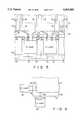
- FIG. 1is an oblique view of two glass panels used in the liquid crystal display panel of the present invention
- FIG. 2is a cross-sectional view of the liquid crystal display panel which employs the glass panels shown in FIG. 1;
- FIG. 3is a block diagram of the liquid crystal display device according to a first embodiment of the present invention and employing the liquid crystal display panel shown in FIG. 2;
- FIG. 4is a front view showing the structure of a part of the liquid crystal display device shown in FIG. 2;
- FIG. 5is a front view showing the structure of a part of the liquid crystal display device according to a second embodiment of the present invention.
- FIG. 6is a front view showing the structure of a part of the liquid crystal display device according to a third embodiment of the present invention.
- FIG. 1is an oblique view of two glass panels used in the liquid crystal display panel of the present invention.
- a plurality of liquid crystal driving voltage wirings 12, which are transparent,are formed at equal intervals on a surface of one glass panel 11.
- a plurality of liquid crystal driving voltage wirings 14, which are transparent,are formed at equal intervals on a surface of the other glass panel 13.
- the wirings 12are called, in this case, scanning wirings, while the wirings 14 are called signal wirings.
- the two glass panels 11 and 13are affixed to each other with a liquid crystal 15 sandwiched therebetween, thus forming a liquid crystal panel 16. More precisely, the glass panels 11 and 13 are affixed to each other such that the wirings 12 on the glass panel 11 and wirings 14 on the glass panel 13 are located inward and in contact with the liquid crystal 15, and such that the wirings 12 cross the wirings 14.
- a plurality of display segmentsare formed on the regions where the wirings 12 cross the wirings 14.
- FIG. 3shows the liquid crystal display device using the above-mentioned liquid crystal panel 16, according to the first embodiment of the present invention.
- a plurality of semiconductor integrated circuit (IC) chips 18are formed around the panel 16 such that they surround the panel.
- These IC chips 18are of the tape automated bonding (TAB) type, and the electrode pads of the IC chips are coupled to the wirings formed on insulating resin films (not shown).
- the IC chips 18generate the liquid crystal driving voltages, i.e., a scanning voltage and a signal voltage, which are applied to the liquid crystal driving voltage wirings mentioned above.
- the liquid crystal display panel 16has a first region 21 in which the liquid crystal is provided between the two glass panels and a large number of display pixels are formed, and a second region 22 in which the liquid crystal is not present between the two glass panels.
- the liquid crystal driving voltages generated by the semiconductor IC chips 18are applied to wiring groups 24 consisting of the wirings 12 or 14 of the liquid crystal display panel 16, through wiring groups 23 consisting of a plurality of liquid crystal driving voltage wirings formed on the above-mentioned insulating resin films.
- wiring groups 25consisting of a plurality of wirings are formed on the insulating resin films.
- Wiring groups 25are electrically connected to one another by a wiring group 26 consisting of a plurality of wirings which are provided on the liquid crystal display panel 16 and which are made of the same material as that of the wirings 12 and 14, e.g. ITO (Indium.TIN.oxide).
- the signals as transmitted through the wiring groups 25 and 26are, for example, control signals such as a shift clock signal, a frame signal, a latch signal, an enable signal and a data signal.
- the voltages as transmitted through a wiring groups 25 and 26are, for example, a ground voltage of e.g. 0 V, a high voltage of e.g. 5 V for a logical operation, a high lighting voltage of e.g. 0 V for a liquid crystal drive, a high non-lighting voltage to e.g. -4 V for a liquid crystal drive, a low non-lighting voltage of e.g. -26 V for a liquid crystal drive, and a low lighting voltage of e.g. -30 V for a liquid crystal drive.
- the wiring group 26is formed in the aforementioned second region 22 in which the liquid crystal is not present, so that the various control signals and voltages transmitted/supplied through the wiring groups 26 do not adversely affect a display operation performed by the liquid crystal display panel.
- FIG. 4is a view showing the structure of a part of the liquid crystal display device shown in FIG. 3.
- the structural elements which correspond to those shown in FIGS. 1-3are denoted by the same reference numerals as those used in FIGS. 1-3, and explanations thereof will be omitted.
- reference numeral 31represents TAB type insulating resin films to which the semiconductor integrated circuit chips 18 are fixed.
- Reference numeral 32denotes wirings arranged on the insulating resin films and which form the wiring groups 23 and 25.
- Reference numeral 33indicates wirings provided on the liquid crystal display panel 16 and which form the wiring group 26. In practice, openings are formed one in each of the TAB type insulating resin films, and the semiconductor IC chips are mounted in their corresponding openings.
- the liquid crystal driving IC chips 18are connected to one another by the wiring groups 25 and 26.
- the timing at which the IC chips are driven, etc.can be controlled without wirings on a printed circuit board being used as in a conventional liquid crystal display device, with the result that the need for a printed circuit board, which is necessary in a conventional liquid crystal display device, is eliminated, thus realizing a compact, thin, and light liquid crystal display device.
- the elimination of the need for the printed circuit boardresults in a reduction in the number of parts used and makes unnecessary a process, which is conventionally performed, for coupling the liquid crystal driving IC chips and the printed circuit board to one another, thus reducing the cost of the device.
- electric characteristics such as signal delay in the wirings 12 and 14 of the display panel 16can be evaluated from monitored electric characters such as signal delay in the wirings 33.
- the liquid crystal driving voltages applied to the display panel 16can be optimized. Therefore, in the case where a plurality of liquid crystal display signals of the same type as that of the display panel 16 are manufactured, even if display panels having different operation characteristics should be produced due to, for example, the differences in the conditions under which those panels are manufactured, the differences in the operation characteristics can be minimized. Further, the matching between the liquid crystal display panels and their liquid crystal driving ICs can be optimized. Thus, high-performance liquid crystal display panels which are improved in terms of the quality of characters or images displayed can be attained.
- FIG. 5is a view showing a part of the liquid crystal display device according to the second embodiment of the present invention.
- a printed circuit board 41is provided around the liquid crystal display panel 16 as in a conventional liquid crystal display panel, and the insulating resin films 31 to which the semiconductor IC chips 18 are fixed are bonded onto the board 41.
- a plurality of wirings 42are formed on the board 41.
- various control signals and voltagesare transmitted/applied through the wirings 32 and 33.
- one or more of the control signals and voltagesare transmitted/applied via wirings 42.
- a ground voltage of 0 Va high voltage of 5 V for a logic operation
- a high lighting voltage of 0 V for a liquid crystal drivea high non-lighting voltage of -4 V for a liquid crystal drive
- a low non-lighting voltage of -26 V for a liquid crystal drivea low lighting voltage of -30 V for a liquid crystal drive are applied through the wirings 42.
- a printed circuit boardis used as in a conventional liquid crystal display panel.
- one or more of the control signals and voltages to be transmitted between the semiconductor IC chipsare transmitted through the wirings provided on the liquid crystal display panel 16. Adopting this technique, the printed circuit board 41 can be reduced in size, making it possible to form a compact liquid crystal display device.
- FIG. 6is a schematic diagram of the liquid crystal display device according to the third embodiment of the present invention.
- a wiring 51is formed on one of the two glass panels forming the liquid crystal display panel 16, and a wiring 52 is formed on the other of the two glass panels.
- the wirings 51 and 52are formed such that they cross each other with the liquid crystal sandwiched therebetween.
- Each of these wirings 51 and 52extends from an end portion of the panel up to the first region 21 in which the liquid crystal is provided.
- each of the liquid crystal display pixelsis equivalent to a capacitor.
- the width of the wirings 51 and 52is equal to that of the wirings 12 and 14, the capacitance existing between the wirings 51 and 52 is equal to the pixel capacitance. Accordingly, by electrically connecting the wirings 51 and 52 to the two semiconductor IC chips 18 and by incorporating a monitoring circuit in the IC chips 18, the characteristics of the display pixels can be monitored.
Landscapes
- Physics & Mathematics (AREA)
- Nonlinear Science (AREA)
- Mathematical Physics (AREA)
- Chemical & Material Sciences (AREA)
- Crystallography & Structural Chemistry (AREA)
- General Physics & Mathematics (AREA)
- Optics & Photonics (AREA)
- Liquid Crystal (AREA)
- Liquid Crystal Display Device Control (AREA)
Abstract
Description
This application is a continuation of application Ser. No. 08/074,974 filed Jun. 10, 1994, now abandoned, which is a continuation of application Ser. No. 07/700,414 filed May 15, 1991, now abandoned.
1. Field of the Invention
The present invention relates to a liquid crystal display panel and a liquid crystal display device using the liquid crystal display panel.
2. Description of the Related Art
A liquid crystal display panel includes two glass panels, between which a liquid crystal is sandwiched and on each of which a plurality of transparent electrodes (or wirings) are arranged in order. In a liquid crystal display device, a printed circuit board, on which a plurality of semiconductor integrated circuit (IC) chips and the like for driving the liquid crystal display panel are mounted, is arranged around the panel. The transparent wirings of the liquid crystal display panel are applied with the driving voltages generated by the semiconductor IC chips, thus causing the display panel to perform a display operation.
In a conventional liquid crystal display device, a plurality of semiconductor IC chips are mounted on a printed circuit board, and patterns of control signal wirings, power supply wirings, etc. which are used for controlling the timing at which the semiconductor IC chips are driven, are formed on the printed circuit board.
Recently, the number of semiconductor IC chips for driving liquid crystal display panels has been increasing in accordance with increases in the size of the display panels. The number of wirings used for signal transmissions between semiconductor IC chips mounted on a printed circuit board has been correspondingly increasing, which necessitates an increase in the size of the printed circuit board. However, the use of a large printed circuit board results in a large and heavy liquid crystal display device produced at high cost.
Moreover, in connection with an increase in the panel size, another requirement is to check the differences in the characteristics of a plurality of liquid crystal display panels, which may result from differences in the conditions, as well as to check electric characteristics such as signal delay in wirings when liquid crystal display panels are applied with liquid crystal driving voltages generated by liquid crystal driving IC chips. However, since a conventional liquid crystal display panel does not have wirings other than those for application of the driving voltages, the operation characteristics of the display panel cannot be externally monitored.
As mentioned above, a conventional liquid crystal display panel has the drawback that the operation characteristics of the display panel and electric characteristics such as signal delay in wirings cannot be externally monitored.
Further, a conventional liquid crystal display device is large in size, heavy, and high in cost, owing to an increase in the panel size.
It is the first object of the present invention to provide a liquid crystal display panel wherein the operation characteristics thereof can be externally monitored.
It is the second object of the present invention to provide a compact, thin, and light liquid crystal display device of low cost which does not require a printed circuit board on which a plurality of liquid crystal driving IC chips are mounted.
According to the present invention, there is provided a liquid crystal display panel comprising: a pair of glass panels, each of which has two major surfaces; a liquid crystal sandwiched between the glass panels so as to be in contact with one major surface of each of the glass panels; a plurality of first light-transmitting wiring means, formed on each of those major surfaces of the glass panels which are in contact with the liquid crystal, and through which a voltage for driving the liquid crystal is applied; and at least one second light-transmitting wiring means formed on at least one of those major surfaces which are in contact with the liquid crystal.
Further, according to the present invention, there is provided a liquid crystal display device comprising: a liquid crystal display panel including a pair of glass panels each of which has two major surfaces, a liquid crystal sandwiched between the glass panels so as to be in contact with one major surface of each of the glass panels, a plurality of first light-transmitting wiring means, formed on each of those major surfaces of the glass panels which are in contact with the liquid crystal, and through which a plurality of voltages for driving the liquid crystal are applied, and at least one second light-transmitting wiring means formed on at least one of those major surfaces which are in contact with the liquid crystal; and a plurality of integrated circuit chips for generating the voltages for driving the liquid crystal.
Additional objects and advantages of the invention will be set forth in the description which follows, and in part will be obvious from the description, or may be learned by practice of the invention. The objects and advantages of the invention may be realized and obtained by means of the instrumentalities and combinations particularly pointed out in the appended claims.
The accompanying drawings, which are incorporated in and constitute a part of the specification, illustrate presently preferred embodiments of the invention, and together with the general description given above and the detailed description of the preferred embodiments given below, serve to explain the principles of the invention.
FIG. 1 is an oblique view of two glass panels used in the liquid crystal display panel of the present invention;
FIG. 2 is a cross-sectional view of the liquid crystal display panel which employs the glass panels shown in FIG. 1;
FIG. 3 is a block diagram of the liquid crystal display device according to a first embodiment of the present invention and employing the liquid crystal display panel shown in FIG. 2;
FIG. 4 is a front view showing the structure of a part of the liquid crystal display device shown in FIG. 2;
FIG. 5 is a front view showing the structure of a part of the liquid crystal display device according to a second embodiment of the present invention; and
FIG. 6 is a front view showing the structure of a part of the liquid crystal display device according to a third embodiment of the present invention.
Embodiments of the present invention will now be described in detail, with reference to the drawings.
FIG. 1 is an oblique view of two glass panels used in the liquid crystal display panel of the present invention. A plurality of liquid crystaldriving voltage wirings 12, which are transparent, are formed at equal intervals on a surface of one glass panel 11. Likewise, a plurality of liquid crystaldriving voltage wirings 14, which are transparent, are formed at equal intervals on a surface of theother glass panel 13. Thewirings 12 are called, in this case, scanning wirings, while thewirings 14 are called signal wirings.
As is shown in FIG. 2, the twoglass panels 11 and 13 are affixed to each other with aliquid crystal 15 sandwiched therebetween, thus forming aliquid crystal panel 16. More precisely, theglass panels 11 and 13 are affixed to each other such that thewirings 12 on the glass panel 11 andwirings 14 on theglass panel 13 are located inward and in contact with theliquid crystal 15, and such that thewirings 12 cross thewirings 14.
Further, a plurality of display segments are formed on the regions where thewirings 12 cross thewirings 14.
FIG. 3 shows the liquid crystal display device using the above-mentionedliquid crystal panel 16, according to the first embodiment of the present invention. A plurality of semiconductor integrated circuit (IC) chips 18 (only two of them are shown in the drawings) are formed around thepanel 16 such that they surround the panel. TheseIC chips 18 are of the tape automated bonding (TAB) type, and the electrode pads of the IC chips are coupled to the wirings formed on insulating resin films (not shown). TheIC chips 18 generate the liquid crystal driving voltages, i.e., a scanning voltage and a signal voltage, which are applied to the liquid crystal driving voltage wirings mentioned above.
The liquidcrystal display panel 16 has afirst region 21 in which the liquid crystal is provided between the two glass panels and a large number of display pixels are formed, and asecond region 22 in which the liquid crystal is not present between the two glass panels.
The liquid crystal driving voltages generated by thesemiconductor IC chips 18 are applied towiring groups 24 consisting of thewirings crystal display panel 16, throughwiring groups 23 consisting of a plurality of liquid crystal driving voltage wirings formed on the above-mentioned insulating resin films.
In addition to thewiring groups 23,wiring groups 25 consisting of a plurality of wirings are formed on the insulating resin films.Wiring groups 25 are electrically connected to one another by awiring group 26 consisting of a plurality of wirings which are provided on the liquidcrystal display panel 16 and which are made of the same material as that of thewirings
Various control signals and voltages which are necessary for the operation of thesemiconductor IC chips 18 are transmitted/applied to theIC chips 18 through thewiring groups wiring groups wiring groups
As shown in the drawings, thewiring group 26 is formed in the aforementionedsecond region 22 in which the liquid crystal is not present, so that the various control signals and voltages transmitted/supplied through thewiring groups 26 do not adversely affect a display operation performed by the liquid crystal display panel.
FIG. 4 is a view showing the structure of a part of the liquid crystal display device shown in FIG. 3. In FIG. 4, the structural elements which correspond to those shown in FIGS. 1-3 are denoted by the same reference numerals as those used in FIGS. 1-3, and explanations thereof will be omitted. In FIG. 4,reference numeral 31 represents TAB type insulating resin films to which the semiconductorintegrated circuit chips 18 are fixed.Reference numeral 32 denotes wirings arranged on the insulating resin films and which form thewiring groups Reference numeral 33 indicates wirings provided on the liquidcrystal display panel 16 and which form thewiring group 26. In practice, openings are formed one in each of the TAB type insulating resin films, and the semiconductor IC chips are mounted in their corresponding openings.
In the liquid crystal display device explained above, the liquid crystal drivingIC chips 18 are connected to one another by thewiring groups
Moreover, electric characteristics such as signal delay in thewirings display panel 16 can be evaluated from monitored electric characters such as signal delay in thewirings 33. In consideration of the electric characteristics monitored, the liquid crystal driving voltages applied to thedisplay panel 16 can be optimized. Therefore, in the case where a plurality of liquid crystal display signals of the same type as that of thedisplay panel 16 are manufactured, even if display panels having different operation characteristics should be produced due to, for example, the differences in the conditions under which those panels are manufactured, the differences in the operation characteristics can be minimized. Further, the matching between the liquid crystal display panels and their liquid crystal driving ICs can be optimized. Thus, high-performance liquid crystal display panels which are improved in terms of the quality of characters or images displayed can be attained.
FIG. 5 is a view showing a part of the liquid crystal display device according to the second embodiment of the present invention. In the second embodiment, a printedcircuit board 41 is provided around the liquidcrystal display panel 16 as in a conventional liquid crystal display panel, and the insulatingresin films 31 to which thesemiconductor IC chips 18 are fixed are bonded onto theboard 41.
A plurality ofwirings 42 are formed on theboard 41. In the first embodiment, various control signals and voltages are transmitted/applied through thewirings wirings 42. For example, a ground voltage of 0 V, a high voltage of 5 V for a logic operation, a high lighting voltage of 0 V for a liquid crystal drive, a high non-lighting voltage of -4 V for a liquid crystal drive, a low non-lighting voltage of -26 V for a liquid crystal drive, and a low lighting voltage of -30 V for a liquid crystal drive are applied through thewirings 42.
In the second embodiment, a printed circuit board is used as in a conventional liquid crystal display panel. However, one or more of the control signals and voltages to be transmitted between the semiconductor IC chips are transmitted through the wirings provided on the liquidcrystal display panel 16. Adopting this technique, the printedcircuit board 41 can be reduced in size, making it possible to form a compact liquid crystal display device.
FIG. 6 is a schematic diagram of the liquid crystal display device according to the third embodiment of the present invention.
In the third embodiment, in addition to thewirings wiring 51 is formed on one of the two glass panels forming the liquidcrystal display panel 16, and awiring 52 is formed on the other of the two glass panels. In other words, thewirings wirings first region 21 in which the liquid crystal is provided.
Incidentally, each of the liquid crystal display pixels is equivalent to a capacitor. When the width of thewirings wirings wirings wirings semiconductor IC chips 18 and by incorporating a monitoring circuit in the IC chips 18, the characteristics of the display pixels can be monitored.
Additional advantages and modifications will readily occur to those skilled in the art. Therefore, the invention in its broader aspects is not limited to the specific details, and representative devices, shown and described herein. Accordingly, various modifications may be made without departing from the spirit or scope of the general inventive concept as defined by the appended claims and their equivalents.
Claims (4)
1. A liquid crystal display device comprising:
a liquid crystal display panel including a pair of glass panels equal to each other in size, said glass panels respectively having central portions between which a liquid crystal is sealed, and peripheral portions between which no liquid crystal is sealed, said liquid crystal display panel further including a plurality of optically-transparent driving wirings formed between said central portions of said glass panels, for conducting a liquid crystal-driving voltage;
a plurality of semiconductor chips each located around said liquid crystal display panel and each installed on a separate flexible film projecting from a peripheral portion of the glass panels, said semiconductor chips being electrically connected to said driving wirings of said liquid crystal display panel and supplying said liquid crystal-driving voltage to said driving wirings; and
a plurality of first wirings formed on a peripheral portion of at least one of said glass panels, second wirings on each flexible film, connected to each semiconductor chip, and extending toward the liquid crystal display panel for connecting at least two of said semiconductor chips which are adjacent to each other, said first and second wirings thereby connecting all of said semiconductor chips in common via each of said semiconductor chips.
2. A liquid crystal display device according to claim 1, wherein said semiconductor chips are bonded onto said flexible film by a tape automated bonding (TAB) method.
3. A liquid crystal display device according to claim 1, wherein said first wirings formed on said glass panels transmit control signals including at least one of a shift clock signal, a frame signal, a latch signal, and a data signal.
4. A liquid crystal display device according to claim 1, wherein said first wirings formed on said glass panels have a power voltage applied thereto for driving each of said semiconductor chips.
Priority Applications (1)
| Application Number | Priority Date | Filing Date | Title |
|---|---|---|---|
| US08/258,379US5565885A (en) | 1990-05-16 | 1994-06-10 | Liquid crystal display panel and liquid crystal display device |
Applications Claiming Priority (5)
| Application Number | Priority Date | Filing Date | Title |
|---|---|---|---|
| JP2125702AJP2554769B2 (en) | 1990-05-16 | 1990-05-16 | Liquid crystal display |
| JP2-125702 | 1990-05-16 | ||
| US70041491A | 1991-05-15 | 1991-05-15 | |
| US7497494A | 1994-06-10 | 1994-06-10 | |
| US08/258,379US5565885A (en) | 1990-05-16 | 1994-06-10 | Liquid crystal display panel and liquid crystal display device |
Related Parent Applications (1)
| Application Number | Title | Priority Date | Filing Date |
|---|---|---|---|
| US7497494AContinuation | 1990-05-16 | 1994-06-10 |
Publications (1)
| Publication Number | Publication Date |
|---|---|
| US5565885Atrue US5565885A (en) | 1996-10-15 |
Family
ID=14916609
Family Applications (1)
| Application Number | Title | Priority Date | Filing Date |
|---|---|---|---|
| US08/258,379Expired - LifetimeUS5565885A (en) | 1990-05-16 | 1994-06-10 | Liquid crystal display panel and liquid crystal display device |
Country Status (3)
| Country | Link |
|---|---|
| US (1) | US5565885A (en) |
| JP (1) | JP2554769B2 (en) |
| KR (1) | KR950009069B1 (en) |
Cited By (76)
| Publication number | Priority date | Publication date | Assignee | Title |
|---|---|---|---|---|
| US5930026A (en)* | 1996-10-25 | 1999-07-27 | Massachusetts Institute Of Technology | Nonemissive displays and piezoelectric power supplies therefor |
| US5940056A (en)* | 1996-04-15 | 1999-08-17 | Kabushiki Kaisha Toshiba | Liquid crystal display device |
| US5961804A (en)* | 1997-03-18 | 1999-10-05 | Massachusetts Institute Of Technology | Microencapsulated electrophoretic display |
| US6067185A (en) | 1997-08-28 | 2000-05-23 | E Ink Corporation | Process for creating an encapsulated electrophoretic display |
| US6120839A (en) | 1995-07-20 | 2000-09-19 | E Ink Corporation | Electro-osmotic displays and materials for making the same |
| US6124851A (en) | 1995-07-20 | 2000-09-26 | E Ink Corporation | Electronic book with multiple page displays |
| US6177921B1 (en) | 1997-08-28 | 2001-01-23 | E Ink Corporation | Printable electrode structures for displays |
| US6232950B1 (en) | 1997-08-28 | 2001-05-15 | E Ink Corporation | Rear electrode structures for displays |
| US6249271B1 (en) | 1995-07-20 | 2001-06-19 | E Ink Corporation | Retroreflective electrophoretic displays and materials for making the same |
| US6262833B1 (en) | 1998-10-07 | 2001-07-17 | E Ink Corporation | Capsules for electrophoretic displays and methods for making the same |
| US6262706B1 (en) | 1995-07-20 | 2001-07-17 | E Ink Corporation | Retroreflective electrophoretic displays and materials for making the same |
| US6300932B1 (en) | 1997-08-28 | 2001-10-09 | E Ink Corporation | Electrophoretic displays with luminescent particles and materials for making the same |
| US6312304B1 (en) | 1998-12-15 | 2001-11-06 | E Ink Corporation | Assembly of microencapsulated electronic displays |
| US6376828B1 (en) | 1998-10-07 | 2002-04-23 | E Ink Corporation | Illumination system for nonemissive electronic displays |
| US6377387B1 (en) | 1999-04-06 | 2002-04-23 | E Ink Corporation | Methods for producing droplets for use in capsule-based electrophoretic displays |
| US20020063661A1 (en)* | 2000-11-29 | 2002-05-30 | E Ink Corporation | Addressing schemes for electronic displays |
| US6445489B1 (en) | 1998-03-18 | 2002-09-03 | E Ink Corporation | Electrophoretic displays and systems for addressing such displays |
| US20020140654A1 (en)* | 1999-04-16 | 2002-10-03 | Kim Sang-Soo | Signal transmission film and a liquid crystal display panel having the same |
| US6473072B1 (en) | 1998-05-12 | 2002-10-29 | E Ink Corporation | Microencapsulated electrophoretic electrostatically-addressed media for drawing device applications |
| US6480182B2 (en) | 1997-03-18 | 2002-11-12 | Massachusetts Institute Of Technology | Printable electronic display |
| US6498114B1 (en) | 1999-04-09 | 2002-12-24 | E Ink Corporation | Method for forming a patterned semiconductor film |
| US6504524B1 (en) | 2000-03-08 | 2003-01-07 | E Ink Corporation | Addressing methods for displays having zero time-average field |
| US6515649B1 (en) | 1995-07-20 | 2003-02-04 | E Ink Corporation | Suspended particle displays and materials for making the same |
| US6518949B2 (en) | 1998-04-10 | 2003-02-11 | E Ink Corporation | Electronic displays using organic-based field effect transistors |
| US20030031001A1 (en)* | 2001-08-13 | 2003-02-13 | Chi Mei Optoelectronics Corp. | Flat panel display and printed circuit board used therein |
| US6525718B1 (en)* | 1997-02-05 | 2003-02-25 | Sharp Kabushiki Kaisha | Flexible circuit board and liquid crystal display device incorporating the same |
| US6531997B1 (en) | 1999-04-30 | 2003-03-11 | E Ink Corporation | Methods for addressing electrophoretic displays |
| US20030103027A1 (en)* | 1999-04-16 | 2003-06-05 | Kim Sang-Soo | Tape carrier package |
| US6664944B1 (en) | 1995-07-20 | 2003-12-16 | E-Ink Corporation | Rear electrode structures for electrophoretic displays |
| US6664942B1 (en)* | 2000-04-17 | 2003-12-16 | Samsung Electronics Co., Ltd. | Signal transmission film and a liquid crystal display panel having the same |
| USD485294S1 (en) | 1998-07-22 | 2004-01-13 | E Ink Corporation | Electrode structure for an electronic display |
| US6683333B2 (en) | 2000-07-14 | 2004-01-27 | E Ink Corporation | Fabrication of electronic circuit elements using unpatterned semiconductor layers |
| US6693620B1 (en) | 1999-05-03 | 2004-02-17 | E Ink Corporation | Threshold addressing of electrophoretic displays |
| US6704133B2 (en) | 1998-03-18 | 2004-03-09 | E-Ink Corporation | Electro-optic display overlays and systems for addressing such displays |
| US6710540B1 (en) | 1995-07-20 | 2004-03-23 | E Ink Corporation | Electrostatically-addressable electrophoretic display |
| US6724519B1 (en) | 1998-12-21 | 2004-04-20 | E-Ink Corporation | Protective electrodes for electrophoretic displays |
| US6727881B1 (en) | 1995-07-20 | 2004-04-27 | E Ink Corporation | Encapsulated electrophoretic displays and methods and materials for making the same |
| US20040090415A1 (en)* | 1995-07-20 | 2004-05-13 | E-Ink Corporation | Rear electrode structures for electrophoretic displays |
| US20040113884A1 (en)* | 1995-07-20 | 2004-06-17 | E Ink Corporation | Electrostatically addressable electrophoretic display |
| US20040224598A1 (en)* | 2002-10-16 | 2004-11-11 | Shuichi Tanaka | Display structure, method of manufacturing display structure, and electronic apparatus |
| US6825068B2 (en) | 2000-04-18 | 2004-11-30 | E Ink Corporation | Process for fabricating thin film transistors |
| US6839158B2 (en) | 1997-08-28 | 2005-01-04 | E Ink Corporation | Encapsulated electrophoretic displays having a monolayer of capsules and materials and methods for making the same |
| US6842657B1 (en) | 1999-04-09 | 2005-01-11 | E Ink Corporation | Reactive formation of dielectric layers and protection of organic layers in organic semiconductor device fabrication |
| US6864875B2 (en) | 1998-04-10 | 2005-03-08 | E Ink Corporation | Full color reflective display with multichromatic sub-pixels |
| US6865010B2 (en) | 2001-12-13 | 2005-03-08 | E Ink Corporation | Electrophoretic electronic displays with low-index films |
| US20050110018A1 (en)* | 2002-01-18 | 2005-05-26 | Van Der Vleuten Renatus J. | Display device with picture decoding |
| US6900851B2 (en) | 2002-02-08 | 2005-05-31 | E Ink Corporation | Electro-optic displays and optical systems for addressing such displays |
| US20050140700A1 (en)* | 2002-01-18 | 2005-06-30 | Van Der Vleuten Renatus J. | Display device whose display area is divided in groups of pixels; each group provided with scaling means |
| US6967640B2 (en) | 2001-07-27 | 2005-11-22 | E Ink Corporation | Microencapsulated electrophoretic display with integrated driver |
| US7002728B2 (en) | 1997-08-28 | 2006-02-21 | E Ink Corporation | Electrophoretic particles, and processes for the production thereof |
| US7030412B1 (en) | 1999-05-05 | 2006-04-18 | E Ink Corporation | Minimally-patterned semiconductor devices for display applications |
| US7038655B2 (en) | 1999-05-03 | 2006-05-02 | E Ink Corporation | Electrophoretic ink composed of particles with field dependent mobilities |
| US7071913B2 (en) | 1995-07-20 | 2006-07-04 | E Ink Corporation | Retroreflective electrophoretic displays and materials for making the same |
| US7109968B2 (en) | 1995-07-20 | 2006-09-19 | E Ink Corporation | Non-spherical cavity electrophoretic displays and methods and materials for making the same |
| US7167155B1 (en) | 1995-07-20 | 2007-01-23 | E Ink Corporation | Color electrophoretic displays |
| US7176880B2 (en) | 1999-07-21 | 2007-02-13 | E Ink Corporation | Use of a storage capacitor to enhance the performance of an active matrix driven electronic display |
| CN1302367C (en)* | 2000-12-29 | 2007-02-28 | Lg菲利浦Lcd株式会社 | Combined structure for touch controller in liquid crystal display plate combined with touch board and liquid crystal display device assembly controller |
| US7230750B2 (en) | 2001-05-15 | 2007-06-12 | E Ink Corporation | Electrophoretic media and processes for the production thereof |
| US7242513B2 (en) | 1997-08-28 | 2007-07-10 | E Ink Corporation | Encapsulated electrophoretic displays having a monolayer of capsules and materials and methods for making the same |
| US7247379B2 (en) | 1997-08-28 | 2007-07-24 | E Ink Corporation | Electrophoretic particles, and processes for the production thereof |
| US7256766B2 (en) | 1998-08-27 | 2007-08-14 | E Ink Corporation | Electrophoretic display comprising optical biasing element |
| US7312916B2 (en) | 2002-08-07 | 2007-12-25 | E Ink Corporation | Electrophoretic media containing specularly reflective particles |
| US20080062348A1 (en)* | 1992-03-12 | 2008-03-13 | Masumi Sasuga | Structure Of Liquid Crystal Display Device For Easy Assembly And Disassembly |
| US20080117495A1 (en)* | 1995-07-20 | 2008-05-22 | E Ink Corporation | Dielectrophoretic displays |
| US7667684B2 (en) | 1998-07-08 | 2010-02-23 | E Ink Corporation | Methods for achieving improved color in microencapsulated electrophoretic devices |
| CN101673522A (en)* | 2008-09-10 | 2010-03-17 | 奇景光电股份有限公司 | Panel device for chip on glass package |
| USRE41669E1 (en) | 2002-05-10 | 2010-09-14 | Ponnusamy Palanisamy | Low-cost circuit board materials and processes for area array electrical interconnections over a large area between a device and the circuit board |
| USRE41914E1 (en) | 2002-05-10 | 2010-11-09 | Ponnusamy Palanisamy | Thermal management in electronic displays |
| US7893435B2 (en) | 2000-04-18 | 2011-02-22 | E Ink Corporation | Flexible electronic circuits and displays including a backplane comprising a patterned metal foil having a plurality of apertures extending therethrough |
| US7957054B1 (en) | 2009-12-21 | 2011-06-07 | Hewlett-Packard Development Company, L.P. | Electro-optical display systems |
| US8089687B2 (en) | 2009-12-21 | 2012-01-03 | Hewlett-Packard Development Company, L.P. | Electro-optical display systems |
| US8115729B2 (en) | 1999-05-03 | 2012-02-14 | E Ink Corporation | Electrophoretic display element with filler particles |
| US8139050B2 (en) | 1995-07-20 | 2012-03-20 | E Ink Corporation | Addressing schemes for electronic displays |
| US9005494B2 (en) | 2004-01-20 | 2015-04-14 | E Ink Corporation | Preparation of capsules |
| US9664978B2 (en) | 2002-10-16 | 2017-05-30 | E Ink Corporation | Electrophoretic displays |
| US11250794B2 (en) | 2004-07-27 | 2022-02-15 | E Ink Corporation | Methods for driving electrophoretic displays using dielectrophoretic forces |
Families Citing this family (5)
| Publication number | Priority date | Publication date | Assignee | Title |
|---|---|---|---|---|
| ES2644690T3 (en) | 2003-03-26 | 2017-11-30 | Daikin Industries, Ltd. | Indoor unit for air conditioner |
| AU2005260872B2 (en)* | 2004-07-14 | 2008-06-26 | Daikin Industries, Ltd. | Indoor unit of an air conditioner |
| JP4923639B2 (en)* | 2005-11-11 | 2012-04-25 | ダイキン工業株式会社 | Indoor panel of air conditioner and air conditioner |
| JP4924695B2 (en)* | 2009-11-04 | 2012-04-25 | ダイキン工業株式会社 | Air conditioner |
| WO2014032229A1 (en) | 2012-08-28 | 2014-03-06 | 广东美的制冷设备有限公司 | Air conditioning indoor machine |
Citations (20)
| Publication number | Priority date | Publication date | Assignee | Title |
|---|---|---|---|---|
| US4655551A (en)* | 1984-01-13 | 1987-04-07 | Sharp Kabushiki Kaisha | Liquid crystal display with chip projecting above and below flexible film |
| JPS62164027A (en)* | 1986-01-14 | 1987-07-20 | Fujitsu Ltd | liquid crystal display device |
| US4684974A (en)* | 1984-11-16 | 1987-08-04 | Matsushita Electric Industrial Co. Ltd. | Electrode connection structure of flat device |
| US4687300A (en)* | 1984-11-09 | 1987-08-18 | Hitachi, Ltd. | Liquid crystal display device |
| JPS6398636A (en)* | 1986-10-16 | 1988-04-30 | Fujitsu Ltd | Adaptive driving method for liquid crystal display device |
| JPS63170618A (en)* | 1987-01-08 | 1988-07-14 | Fujitsu Ltd | liquid crystal display device |
| US4766426A (en)* | 1985-02-14 | 1988-08-23 | Matsushita Electric Industrial Co., Ltd. | Display panel assembly having a plurality of film carrier tapes on each of which a semiconductor divice is mounted |
| US4772100A (en)* | 1986-10-09 | 1988-09-20 | Oki Electric Industry Co. Ltd. | Liquid crystal display device having circuit boards extending along segment and column electrode directions |
| US4832455A (en)* | 1986-09-11 | 1989-05-23 | Kabushiki Kaisha Toshia | Liquid crystal apparatus having an anisotropic conductive layer between the lead electrodes of the liquid crystal device and the circuit board |
| US4836651A (en)* | 1987-12-03 | 1989-06-06 | Anderson Richard A | Flexible circuit interconnection for a matrix addressed liquid crystal panel |
| US4840459A (en)* | 1987-11-03 | 1989-06-20 | General Electric Co. | Matrix addressed flat panel liquid crystal display device with dual ended auxiliary repair lines for address line repair |
| US4862153A (en)* | 1986-05-30 | 1989-08-29 | Sharp Kabushiki Kaisha | Flat display panel with framing for flexible substrate folding |
| US4896946A (en)* | 1985-05-13 | 1990-01-30 | Ricoh Company, Ltd. | Liquid crystal display device |
| US4917466A (en)* | 1987-08-13 | 1990-04-17 | Shin-Etsu Polymer Co., Ltd. | Method for electrically connecting IC chips, a resinous bump-forming composition used therein and a liquid-crystal display unit electrically connected thereby |
| US5016986A (en)* | 1988-04-12 | 1991-05-21 | Sharp Kabushiki Kaisha | Display device having an improvement in insulating between conductors connected to electronic components |
| US5028916A (en)* | 1984-09-28 | 1991-07-02 | Kabushiki Kaisha Toshiba | Active matrix display device |
| US5042919A (en)* | 1987-05-01 | 1991-08-27 | Canon Kabushiki Kaisha | External-circuit connecting and packaging structure |
| US5049866A (en)* | 1988-07-26 | 1991-09-17 | Citizen Watch Co., Ltd. | Liquid crystal display device |
| US5117300A (en)* | 1989-04-05 | 1992-05-26 | Licentia Patent-Verwaltungs-Gmbh | Electrical circuit device with different types of conductor paths |
| US5293262A (en)* | 1988-03-15 | 1994-03-08 | Mitsubishi Denki Kabushiki Kaisha | Liquid crystal display device having heat-insulating members and driving circuit boards attached to rear edges of light box |
- 1990
- 1990-05-16JPJP2125702Apatent/JP2554769B2/ennot_activeExpired - Lifetime
- 1991
- 1991-05-15KRKR1019910007835Apatent/KR950009069B1/ennot_activeExpired - Fee Related
- 1994
- 1994-06-10USUS08/258,379patent/US5565885A/ennot_activeExpired - Lifetime
Patent Citations (20)
| Publication number | Priority date | Publication date | Assignee | Title |
|---|---|---|---|---|
| US4655551A (en)* | 1984-01-13 | 1987-04-07 | Sharp Kabushiki Kaisha | Liquid crystal display with chip projecting above and below flexible film |
| US5028916A (en)* | 1984-09-28 | 1991-07-02 | Kabushiki Kaisha Toshiba | Active matrix display device |
| US4687300A (en)* | 1984-11-09 | 1987-08-18 | Hitachi, Ltd. | Liquid crystal display device |
| US4684974A (en)* | 1984-11-16 | 1987-08-04 | Matsushita Electric Industrial Co. Ltd. | Electrode connection structure of flat device |
| US4766426A (en)* | 1985-02-14 | 1988-08-23 | Matsushita Electric Industrial Co., Ltd. | Display panel assembly having a plurality of film carrier tapes on each of which a semiconductor divice is mounted |
| US4896946A (en)* | 1985-05-13 | 1990-01-30 | Ricoh Company, Ltd. | Liquid crystal display device |
| JPS62164027A (en)* | 1986-01-14 | 1987-07-20 | Fujitsu Ltd | liquid crystal display device |
| US4862153A (en)* | 1986-05-30 | 1989-08-29 | Sharp Kabushiki Kaisha | Flat display panel with framing for flexible substrate folding |
| US4832455A (en)* | 1986-09-11 | 1989-05-23 | Kabushiki Kaisha Toshia | Liquid crystal apparatus having an anisotropic conductive layer between the lead electrodes of the liquid crystal device and the circuit board |
| US4772100A (en)* | 1986-10-09 | 1988-09-20 | Oki Electric Industry Co. Ltd. | Liquid crystal display device having circuit boards extending along segment and column electrode directions |
| JPS6398636A (en)* | 1986-10-16 | 1988-04-30 | Fujitsu Ltd | Adaptive driving method for liquid crystal display device |
| JPS63170618A (en)* | 1987-01-08 | 1988-07-14 | Fujitsu Ltd | liquid crystal display device |
| US5042919A (en)* | 1987-05-01 | 1991-08-27 | Canon Kabushiki Kaisha | External-circuit connecting and packaging structure |
| US4917466A (en)* | 1987-08-13 | 1990-04-17 | Shin-Etsu Polymer Co., Ltd. | Method for electrically connecting IC chips, a resinous bump-forming composition used therein and a liquid-crystal display unit electrically connected thereby |
| US4840459A (en)* | 1987-11-03 | 1989-06-20 | General Electric Co. | Matrix addressed flat panel liquid crystal display device with dual ended auxiliary repair lines for address line repair |
| US4836651A (en)* | 1987-12-03 | 1989-06-06 | Anderson Richard A | Flexible circuit interconnection for a matrix addressed liquid crystal panel |
| US5293262A (en)* | 1988-03-15 | 1994-03-08 | Mitsubishi Denki Kabushiki Kaisha | Liquid crystal display device having heat-insulating members and driving circuit boards attached to rear edges of light box |
| US5016986A (en)* | 1988-04-12 | 1991-05-21 | Sharp Kabushiki Kaisha | Display device having an improvement in insulating between conductors connected to electronic components |
| US5049866A (en)* | 1988-07-26 | 1991-09-17 | Citizen Watch Co., Ltd. | Liquid crystal display device |
| US5117300A (en)* | 1989-04-05 | 1992-05-26 | Licentia Patent-Verwaltungs-Gmbh | Electrical circuit device with different types of conductor paths |
Non-Patent Citations (2)
| Title |
|---|
| HV57, HV58, Super tex Inc., pp. 11 130 to pp. 11 134, 1988.* |
| HV57, HV58, Super tex Inc., pp. 11-130 to pp. 11-134, 1988. |
Cited By (118)
| Publication number | Priority date | Publication date | Assignee | Title |
|---|---|---|---|---|
| US20080062348A1 (en)* | 1992-03-12 | 2008-03-13 | Masumi Sasuga | Structure Of Liquid Crystal Display Device For Easy Assembly And Disassembly |
| US8139050B2 (en) | 1995-07-20 | 2012-03-20 | E Ink Corporation | Addressing schemes for electronic displays |
| US7304634B2 (en) | 1995-07-20 | 2007-12-04 | E Ink Corporation | Rear electrode structures for electrophoretic displays |
| US8593718B2 (en) | 1995-07-20 | 2013-11-26 | E Ink Corporation | Electro-osmotic displays and materials for making the same |
| US6120839A (en) | 1995-07-20 | 2000-09-19 | E Ink Corporation | Electro-osmotic displays and materials for making the same |
| US6124851A (en) | 1995-07-20 | 2000-09-26 | E Ink Corporation | Electronic book with multiple page displays |
| US6680725B1 (en) | 1995-07-20 | 2004-01-20 | E Ink Corporation | Methods of manufacturing electronically addressable displays |
| US8305341B2 (en) | 1995-07-20 | 2012-11-06 | E Ink Corporation | Dielectrophoretic displays |
| US6664944B1 (en) | 1995-07-20 | 2003-12-16 | E-Ink Corporation | Rear electrode structures for electrophoretic displays |
| US6249271B1 (en) | 1995-07-20 | 2001-06-19 | E Ink Corporation | Retroreflective electrophoretic displays and materials for making the same |
| US7746544B2 (en) | 1995-07-20 | 2010-06-29 | E Ink Corporation | Electro-osmotic displays and materials for making the same |
| US6262706B1 (en) | 1995-07-20 | 2001-07-17 | E Ink Corporation | Retroreflective electrophoretic displays and materials for making the same |
| US7583251B2 (en) | 1995-07-20 | 2009-09-01 | E Ink Corporation | Dielectrophoretic displays |
| US7391555B2 (en) | 1995-07-20 | 2008-06-24 | E Ink Corporation | Non-spherical cavity electrophoretic displays and materials for making the same |
| US20080117495A1 (en)* | 1995-07-20 | 2008-05-22 | E Ink Corporation | Dielectrophoretic displays |
| US6710540B1 (en) | 1995-07-20 | 2004-03-23 | E Ink Corporation | Electrostatically-addressable electrophoretic display |
| US7352353B2 (en) | 1995-07-20 | 2008-04-01 | E Ink Corporation | Electrostatically addressable electrophoretic display |
| US7109968B2 (en) | 1995-07-20 | 2006-09-19 | E Ink Corporation | Non-spherical cavity electrophoretic displays and methods and materials for making the same |
| US7167155B1 (en) | 1995-07-20 | 2007-01-23 | E Ink Corporation | Color electrophoretic displays |
| US6727881B1 (en) | 1995-07-20 | 2004-04-27 | E Ink Corporation | Encapsulated electrophoretic displays and methods and materials for making the same |
| US7106296B1 (en) | 1995-07-20 | 2006-09-12 | E Ink Corporation | Electronic book with multiple page displays |
| US7071913B2 (en) | 1995-07-20 | 2006-07-04 | E Ink Corporation | Retroreflective electrophoretic displays and materials for making the same |
| US20040090415A1 (en)* | 1995-07-20 | 2004-05-13 | E-Ink Corporation | Rear electrode structures for electrophoretic displays |
| US6515649B1 (en) | 1995-07-20 | 2003-02-04 | E Ink Corporation | Suspended particle displays and materials for making the same |
| US20040113884A1 (en)* | 1995-07-20 | 2004-06-17 | E Ink Corporation | Electrostatically addressable electrophoretic display |
| US5940056A (en)* | 1996-04-15 | 1999-08-17 | Kabushiki Kaisha Toshiba | Liquid crystal display device |
| US5930026A (en)* | 1996-10-25 | 1999-07-27 | Massachusetts Institute Of Technology | Nonemissive displays and piezoelectric power supplies therefor |
| US6130773A (en)* | 1996-10-25 | 2000-10-10 | Massachusetts Institute Of Technology | Nonemissive displays and piezoelectric power supplies therefor |
| US6525718B1 (en)* | 1997-02-05 | 2003-02-25 | Sharp Kabushiki Kaisha | Flexible circuit board and liquid crystal display device incorporating the same |
| US6980196B1 (en) | 1997-03-18 | 2005-12-27 | Massachusetts Institute Of Technology | Printable electronic display |
| US6480182B2 (en) | 1997-03-18 | 2002-11-12 | Massachusetts Institute Of Technology | Printable electronic display |
| US5961804A (en)* | 1997-03-18 | 1999-10-05 | Massachusetts Institute Of Technology | Microencapsulated electrophoretic display |
| US6535197B1 (en) | 1997-08-28 | 2003-03-18 | E Ink Corporation | Printable electrode structures for displays |
| US7242513B2 (en) | 1997-08-28 | 2007-07-10 | E Ink Corporation | Encapsulated electrophoretic displays having a monolayer of capsules and materials and methods for making the same |
| US7002728B2 (en) | 1997-08-28 | 2006-02-21 | E Ink Corporation | Electrophoretic particles, and processes for the production thereof |
| US6445374B2 (en) | 1997-08-28 | 2002-09-03 | E Ink Corporation | Rear electrode structures for displays |
| US6232950B1 (en) | 1997-08-28 | 2001-05-15 | E Ink Corporation | Rear electrode structures for displays |
| US7247379B2 (en) | 1997-08-28 | 2007-07-24 | E Ink Corporation | Electrophoretic particles, and processes for the production thereof |
| US6300932B1 (en) | 1997-08-28 | 2001-10-09 | E Ink Corporation | Electrophoretic displays with luminescent particles and materials for making the same |
| US6067185A (en) | 1997-08-28 | 2000-05-23 | E Ink Corporation | Process for creating an encapsulated electrophoretic display |
| US6839158B2 (en) | 1997-08-28 | 2005-01-04 | E Ink Corporation | Encapsulated electrophoretic displays having a monolayer of capsules and materials and methods for making the same |
| US6392785B1 (en) | 1997-08-28 | 2002-05-21 | E Ink Corporation | Non-spherical cavity electrophoretic displays and materials for making the same |
| US6177921B1 (en) | 1997-08-28 | 2001-01-23 | E Ink Corporation | Printable electrode structures for displays |
| US6842167B2 (en) | 1997-08-28 | 2005-01-11 | E Ink Corporation | Rear electrode structures for displays |
| US6445489B1 (en) | 1998-03-18 | 2002-09-03 | E Ink Corporation | Electrophoretic displays and systems for addressing such displays |
| US6704133B2 (en) | 1998-03-18 | 2004-03-09 | E-Ink Corporation | Electro-optic display overlays and systems for addressing such displays |
| US8466852B2 (en) | 1998-04-10 | 2013-06-18 | E Ink Corporation | Full color reflective display with multichromatic sub-pixels |
| US7075502B1 (en) | 1998-04-10 | 2006-07-11 | E Ink Corporation | Full color reflective display with multichromatic sub-pixels |
| US6518949B2 (en) | 1998-04-10 | 2003-02-11 | E Ink Corporation | Electronic displays using organic-based field effect transistors |
| US6864875B2 (en) | 1998-04-10 | 2005-03-08 | E Ink Corporation | Full color reflective display with multichromatic sub-pixels |
| US6738050B2 (en) | 1998-05-12 | 2004-05-18 | E Ink Corporation | Microencapsulated electrophoretic electrostatically addressed media for drawing device applications |
| US6473072B1 (en) | 1998-05-12 | 2002-10-29 | E Ink Corporation | Microencapsulated electrophoretic electrostatically-addressed media for drawing device applications |
| US7667684B2 (en) | 1998-07-08 | 2010-02-23 | E Ink Corporation | Methods for achieving improved color in microencapsulated electrophoretic devices |
| US9293511B2 (en) | 1998-07-08 | 2016-03-22 | E Ink Corporation | Methods for achieving improved color in microencapsulated electrophoretic devices |
| USD485294S1 (en) | 1998-07-22 | 2004-01-13 | E Ink Corporation | Electrode structure for an electronic display |
| US7256766B2 (en) | 1998-08-27 | 2007-08-14 | E Ink Corporation | Electrophoretic display comprising optical biasing element |
| US6376828B1 (en) | 1998-10-07 | 2002-04-23 | E Ink Corporation | Illumination system for nonemissive electronic displays |
| US6262833B1 (en) | 1998-10-07 | 2001-07-17 | E Ink Corporation | Capsules for electrophoretic displays and methods for making the same |
| US6312304B1 (en) | 1998-12-15 | 2001-11-06 | E Ink Corporation | Assembly of microencapsulated electronic displays |
| US6724519B1 (en) | 1998-12-21 | 2004-04-20 | E-Ink Corporation | Protective electrodes for electrophoretic displays |
| US6377387B1 (en) | 1999-04-06 | 2002-04-23 | E Ink Corporation | Methods for producing droplets for use in capsule-based electrophoretic displays |
| US6498114B1 (en) | 1999-04-09 | 2002-12-24 | E Ink Corporation | Method for forming a patterned semiconductor film |
| US6842657B1 (en) | 1999-04-09 | 2005-01-11 | E Ink Corporation | Reactive formation of dielectric layers and protection of organic layers in organic semiconductor device fabrication |
| US7106317B2 (en) | 1999-04-16 | 2006-09-12 | Samsung Electronics Co., Ltd. | Tape carrier package |
| US20040085279A1 (en)* | 1999-04-16 | 2004-05-06 | Kim Sang-Soo | Flat panel display with signal transmission patterns |
| US20090073100A1 (en)* | 1999-04-16 | 2009-03-19 | Samsung Electronics Col, Ltd. | Signal transmission film and a liquid crystal display panel having the same |
| US8031150B2 (en) | 1999-04-16 | 2011-10-04 | Samsung Electronics Co., Ltd. | Liquid crystal display panel with signal transmission patterns |
| US7102631B2 (en) | 1999-04-16 | 2006-09-05 | Samsung Electronics Co., Ltd. | Display panel with signal transmission patterns |
| US20020140654A1 (en)* | 1999-04-16 | 2002-10-03 | Kim Sang-Soo | Signal transmission film and a liquid crystal display panel having the same |
| US20050190174A1 (en)* | 1999-04-16 | 2005-09-01 | Kim Sang-Soo | Liquid crystal display panel with signal transmission patterns |
| US7295196B2 (en) | 1999-04-16 | 2007-11-13 | Samsung Electronics Co., Ltd. | Liquid crystal display panel with signal transmission patterns |
| US7133037B2 (en) | 1999-04-16 | 2006-11-07 | Samsung Electronics Co., Ltd. | Signal transmission system |
| US7268776B2 (en)* | 1999-04-16 | 2007-09-11 | Samsung Electronics Co., Ltd. | Flat panel display with signal transmission patterns |
| US6639589B1 (en) | 1999-04-16 | 2003-10-28 | Samsung Electronics Co., Ltd. | Tape carrier package and a liquid crystal display panel having the same |
| US20080062109A1 (en)* | 1999-04-16 | 2008-03-13 | Kim Sang-Soo | Liquid crystal display panel with signal transmission patterns |
| US20030201989A1 (en)* | 1999-04-16 | 2003-10-30 | Kim Sang-Soo | Signal transmission system |
| US7339568B2 (en) | 1999-04-16 | 2008-03-04 | Samsung Electronics Co., Ltd. | Signal transmission film and a liquid crystal display panel having the same |
| US20030103027A1 (en)* | 1999-04-16 | 2003-06-05 | Kim Sang-Soo | Tape carrier package |
| US6531997B1 (en) | 1999-04-30 | 2003-03-11 | E Ink Corporation | Methods for addressing electrophoretic displays |
| US6693620B1 (en) | 1999-05-03 | 2004-02-17 | E Ink Corporation | Threshold addressing of electrophoretic displays |
| US7038655B2 (en) | 1999-05-03 | 2006-05-02 | E Ink Corporation | Electrophoretic ink composed of particles with field dependent mobilities |
| US8115729B2 (en) | 1999-05-03 | 2012-02-14 | E Ink Corporation | Electrophoretic display element with filler particles |
| US7030412B1 (en) | 1999-05-05 | 2006-04-18 | E Ink Corporation | Minimally-patterned semiconductor devices for display applications |
| US7859637B2 (en) | 1999-07-21 | 2010-12-28 | E Ink Corporation | Use of a storage capacitor to enhance the performance of an active matrix driven electronic display |
| US7176880B2 (en) | 1999-07-21 | 2007-02-13 | E Ink Corporation | Use of a storage capacitor to enhance the performance of an active matrix driven electronic display |
| US6504524B1 (en) | 2000-03-08 | 2003-01-07 | E Ink Corporation | Addressing methods for displays having zero time-average field |
| US6664942B1 (en)* | 2000-04-17 | 2003-12-16 | Samsung Electronics Co., Ltd. | Signal transmission film and a liquid crystal display panel having the same |
| US7893435B2 (en) | 2000-04-18 | 2011-02-22 | E Ink Corporation | Flexible electronic circuits and displays including a backplane comprising a patterned metal foil having a plurality of apertures extending therethrough |
| US7365394B2 (en) | 2000-04-18 | 2008-04-29 | E Ink Corporation | Process for fabricating thin film transistors |
| US6825068B2 (en) | 2000-04-18 | 2004-11-30 | E Ink Corporation | Process for fabricating thin film transistors |
| US6683333B2 (en) | 2000-07-14 | 2004-01-27 | E Ink Corporation | Fabrication of electronic circuit elements using unpatterned semiconductor layers |
| US20020063661A1 (en)* | 2000-11-29 | 2002-05-30 | E Ink Corporation | Addressing schemes for electronic displays |
| US7023420B2 (en) | 2000-11-29 | 2006-04-04 | E Ink Corporation | Electronic display with photo-addressing means |
| CN1302367C (en)* | 2000-12-29 | 2007-02-28 | Lg菲利浦Lcd株式会社 | Combined structure for touch controller in liquid crystal display plate combined with touch board and liquid crystal display device assembly controller |
| US7375875B2 (en) | 2001-05-15 | 2008-05-20 | E Ink Corporation | Electrophoretic media and processes for the production thereof |
| US7532388B2 (en) | 2001-05-15 | 2009-05-12 | E Ink Corporation | Electrophoretic media and processes for the production thereof |
| US7230750B2 (en) | 2001-05-15 | 2007-06-12 | E Ink Corporation | Electrophoretic media and processes for the production thereof |
| US6967640B2 (en) | 2001-07-27 | 2005-11-22 | E Ink Corporation | Microencapsulated electrophoretic display with integrated driver |
| US7382363B2 (en) | 2001-07-27 | 2008-06-03 | E Ink Corporation | Microencapsulated electrophoretic display with integrated driver |
| US20030031001A1 (en)* | 2001-08-13 | 2003-02-13 | Chi Mei Optoelectronics Corp. | Flat panel display and printed circuit board used therein |
| US6865010B2 (en) | 2001-12-13 | 2005-03-08 | E Ink Corporation | Electrophoretic electronic displays with low-index films |
| US20050110018A1 (en)* | 2002-01-18 | 2005-05-26 | Van Der Vleuten Renatus J. | Display device with picture decoding |
| US20050140700A1 (en)* | 2002-01-18 | 2005-06-30 | Van Der Vleuten Renatus J. | Display device whose display area is divided in groups of pixels; each group provided with scaling means |
| US6900851B2 (en) | 2002-02-08 | 2005-05-31 | E Ink Corporation | Electro-optic displays and optical systems for addressing such displays |
| USRE41914E1 (en) | 2002-05-10 | 2010-11-09 | Ponnusamy Palanisamy | Thermal management in electronic displays |
| USRE42542E1 (en) | 2002-05-10 | 2011-07-12 | Transpacific Infinity, Llc | Low-cost circuit board materials and processes for area array electrical interconnections over a large area between a device and the circuit board |
| USRE41669E1 (en) | 2002-05-10 | 2010-09-14 | Ponnusamy Palanisamy | Low-cost circuit board materials and processes for area array electrical interconnections over a large area between a device and the circuit board |
| US7312916B2 (en) | 2002-08-07 | 2007-12-25 | E Ink Corporation | Electrophoretic media containing specularly reflective particles |
| US10331005B2 (en) | 2002-10-16 | 2019-06-25 | E Ink Corporation | Electrophoretic displays |
| US9664978B2 (en) | 2002-10-16 | 2017-05-30 | E Ink Corporation | Electrophoretic displays |
| US7143504B2 (en)* | 2002-10-16 | 2006-12-05 | Seiko Epson Corporation | Method of manufacturing a display structure |
| US20040224598A1 (en)* | 2002-10-16 | 2004-11-11 | Shuichi Tanaka | Display structure, method of manufacturing display structure, and electronic apparatus |
| US9005494B2 (en) | 2004-01-20 | 2015-04-14 | E Ink Corporation | Preparation of capsules |
| US11250794B2 (en) | 2004-07-27 | 2022-02-15 | E Ink Corporation | Methods for driving electrophoretic displays using dielectrophoretic forces |
| CN101673522A (en)* | 2008-09-10 | 2010-03-17 | 奇景光电股份有限公司 | Panel device for chip on glass package |
| US7957054B1 (en) | 2009-12-21 | 2011-06-07 | Hewlett-Packard Development Company, L.P. | Electro-optical display systems |
| US8089687B2 (en) | 2009-12-21 | 2012-01-03 | Hewlett-Packard Development Company, L.P. | Electro-optical display systems |
| US20110149377A1 (en)* | 2009-12-21 | 2011-06-23 | Jong-Souk Yeo | Electro-optical display systems |
Also Published As
| Publication number | Publication date |
|---|---|
| KR910020472A (en) | 1991-12-20 |
| JP2554769B2 (en) | 1996-11-13 |
| KR950009069B1 (en) | 1995-08-14 |
| JPH0420923A (en) | 1992-01-24 |
Similar Documents
| Publication | Publication Date | Title |
|---|---|---|
| US5565885A (en) | Liquid crystal display panel and liquid crystal display device | |
| US6853430B2 (en) | Display element driving apparatus and display using the same | |
| US6054975A (en) | Liquid crystal display device having tape carrier packages | |
| US7164460B2 (en) | Mounting structure for semiconductor device, electro-optical device, and electronic apparatus | |
| US6025901A (en) | Liquid crystal display device and method for producing the same | |
| US5488498A (en) | Liquid crystal display with particular contacts for supplying counter electrode potential | |
| US20030030604A1 (en) | Liquid crystal display | |
| US5193022A (en) | Plane-type display apparatus | |
| KR100847812B1 (en) | Line on glass liquid crystal display panel | |
| KR20010083972A (en) | Liquid Crystal Display Device and Method of Fabricating the same | |
| KR20040010283A (en) | Liquid crystal display device | |
| KR20020078365A (en) | Driver Intergrated Circuit unit for Liquid Crystal Display Device | |
| JPH09258249A (en) | Semiconductor integrated circuit | |
| KR100194690B1 (en) | Liquid crystal display module | |
| JPH0329925A (en) | liquid crystal display device | |
| KR100294823B1 (en) | Line structure of bottom glass substrate of liquid crystal display device | |
| KR100495855B1 (en) | LCD Display | |
| KR100767362B1 (en) | Liquid crystal display | |
| KR100243812B1 (en) | Structure of FPC of LCD | |
| KR20050121839A (en) | Display device | |
| JP3505265B2 (en) | Film carrier and liquid crystal display device using the same | |
| KR100912693B1 (en) | LCD Display | |
| US20230095839A1 (en) | Array substrate, display panel and driving method thereof | |
| JPH11119245A (en) | Liquid crystal display panel | |
| KR19990024956A (en) | Wiring Structure and Wiring Method of COG Type Liquid Crystal Display Panel |
Legal Events
| Date | Code | Title | Description |
|---|---|---|---|
| STCF | Information on status: patent grant | Free format text:PATENTED CASE | |
| FEPP | Fee payment procedure | Free format text:PAYOR NUMBER ASSIGNED (ORIGINAL EVENT CODE: ASPN); ENTITY STATUS OF PATENT OWNER: LARGE ENTITY | |
| FPAY | Fee payment | Year of fee payment:4 | |
| FPAY | Fee payment | Year of fee payment:8 | |
| FPAY | Fee payment | Year of fee payment:12 |