US5565697A - Semiconductor structure having island forming grooves - Google Patents
Semiconductor structure having island forming groovesDownload PDFInfo
- Publication number
- US5565697A US5565697AUS08/458,800US45880095AUS5565697AUS 5565697 AUS5565697 AUS 5565697AUS 45880095 AUS45880095 AUS 45880095AUS 5565697 AUS5565697 AUS 5565697A
- Authority
- US
- United States
- Prior art keywords
- film
- silicon
- films
- monocrystalline
- semiconductor
- Prior art date
- Legal status (The legal status is an assumption and is not a legal conclusion. Google has not performed a legal analysis and makes no representation as to the accuracy of the status listed.)
- Expired - Fee Related
Links
Images


Classifications
- H—ELECTRICITY
- H01—ELECTRIC ELEMENTS
- H01L—SEMICONDUCTOR DEVICES NOT COVERED BY CLASS H10
- H01L21/00—Processes or apparatus adapted for the manufacture or treatment of semiconductor or solid state devices or of parts thereof
- H01L21/02—Manufacture or treatment of semiconductor devices or of parts thereof
- H01L21/02104—Forming layers
- H01L21/02365—Forming inorganic semiconducting materials on a substrate
- H01L21/02656—Special treatments
- H01L21/02664—Aftertreatments
- H01L21/02667—Crystallisation or recrystallisation of non-monocrystalline semiconductor materials, e.g. regrowth
- H01L21/02675—Crystallisation or recrystallisation of non-monocrystalline semiconductor materials, e.g. regrowth using laser beams
- H01L21/02683—Continuous wave laser beam
- H—ELECTRICITY
- H01—ELECTRIC ELEMENTS
- H01L—SEMICONDUCTOR DEVICES NOT COVERED BY CLASS H10
- H01L21/00—Processes or apparatus adapted for the manufacture or treatment of semiconductor or solid state devices or of parts thereof
- H01L21/02—Manufacture or treatment of semiconductor devices or of parts thereof
- H01L21/02104—Forming layers
- H01L21/02365—Forming inorganic semiconducting materials on a substrate
- H01L21/02367—Substrates
- H01L21/0237—Materials
- H01L21/02373—Group 14 semiconducting materials
- H01L21/02381—Silicon, silicon germanium, germanium
- H—ELECTRICITY
- H01—ELECTRIC ELEMENTS
- H01L—SEMICONDUCTOR DEVICES NOT COVERED BY CLASS H10
- H01L21/00—Processes or apparatus adapted for the manufacture or treatment of semiconductor or solid state devices or of parts thereof
- H01L21/02—Manufacture or treatment of semiconductor devices or of parts thereof
- H01L21/02104—Forming layers
- H01L21/02365—Forming inorganic semiconducting materials on a substrate
- H01L21/02436—Intermediate layers between substrates and deposited layers
- H01L21/02439—Materials
- H01L21/02488—Insulating materials
- H—ELECTRICITY
- H01—ELECTRIC ELEMENTS
- H01L—SEMICONDUCTOR DEVICES NOT COVERED BY CLASS H10
- H01L21/00—Processes or apparatus adapted for the manufacture or treatment of semiconductor or solid state devices or of parts thereof
- H01L21/02—Manufacture or treatment of semiconductor devices or of parts thereof
- H01L21/02104—Forming layers
- H01L21/02365—Forming inorganic semiconducting materials on a substrate
- H01L21/02436—Intermediate layers between substrates and deposited layers
- H01L21/02439—Materials
- H01L21/02491—Conductive materials
- H—ELECTRICITY
- H01—ELECTRIC ELEMENTS
- H01L—SEMICONDUCTOR DEVICES NOT COVERED BY CLASS H10
- H01L21/00—Processes or apparatus adapted for the manufacture or treatment of semiconductor or solid state devices or of parts thereof
- H01L21/02—Manufacture or treatment of semiconductor devices or of parts thereof
- H01L21/02104—Forming layers
- H01L21/02365—Forming inorganic semiconducting materials on a substrate
- H01L21/02436—Intermediate layers between substrates and deposited layers
- H01L21/02494—Structure
- H01L21/02496—Layer structure
- H01L21/02502—Layer structure consisting of two layers
- H—ELECTRICITY
- H01—ELECTRIC ELEMENTS
- H01L—SEMICONDUCTOR DEVICES NOT COVERED BY CLASS H10
- H01L21/00—Processes or apparatus adapted for the manufacture or treatment of semiconductor or solid state devices or of parts thereof
- H01L21/02—Manufacture or treatment of semiconductor devices or of parts thereof
- H01L21/02104—Forming layers
- H01L21/02365—Forming inorganic semiconducting materials on a substrate
- H01L21/02518—Deposited layers
- H01L21/02521—Materials
- H01L21/02524—Group 14 semiconducting materials
- H01L21/02532—Silicon, silicon germanium, germanium
- H—ELECTRICITY
- H01—ELECTRIC ELEMENTS
- H01L—SEMICONDUCTOR DEVICES NOT COVERED BY CLASS H10
- H01L21/00—Processes or apparatus adapted for the manufacture or treatment of semiconductor or solid state devices or of parts thereof
- H01L21/02—Manufacture or treatment of semiconductor devices or of parts thereof
- H01L21/02104—Forming layers
- H01L21/02365—Forming inorganic semiconducting materials on a substrate
- H01L21/02518—Deposited layers
- H01L21/02521—Materials
- H01L21/02538—Group 13/15 materials
- H01L21/02543—Phosphides
- H—ELECTRICITY
- H01—ELECTRIC ELEMENTS
- H01L—SEMICONDUCTOR DEVICES NOT COVERED BY CLASS H10
- H01L21/00—Processes or apparatus adapted for the manufacture or treatment of semiconductor or solid state devices or of parts thereof
- H01L21/02—Manufacture or treatment of semiconductor devices or of parts thereof
- H01L21/02104—Forming layers
- H01L21/02365—Forming inorganic semiconducting materials on a substrate
- H01L21/02518—Deposited layers
- H01L21/02521—Materials
- H01L21/02538—Group 13/15 materials
- H01L21/02546—Arsenides
- H—ELECTRICITY
- H01—ELECTRIC ELEMENTS
- H01L—SEMICONDUCTOR DEVICES NOT COVERED BY CLASS H10
- H01L21/00—Processes or apparatus adapted for the manufacture or treatment of semiconductor or solid state devices or of parts thereof
- H01L21/02—Manufacture or treatment of semiconductor devices or of parts thereof
- H01L21/02104—Forming layers
- H01L21/02365—Forming inorganic semiconducting materials on a substrate
- H01L21/02518—Deposited layers
- H01L21/02587—Structure
- H01L21/0259—Microstructure
- H01L21/02598—Microstructure monocrystalline
- H—ELECTRICITY
- H01—ELECTRIC ELEMENTS
- H01L—SEMICONDUCTOR DEVICES NOT COVERED BY CLASS H10
- H01L21/00—Processes or apparatus adapted for the manufacture or treatment of semiconductor or solid state devices or of parts thereof
- H01L21/02—Manufacture or treatment of semiconductor devices or of parts thereof
- H01L21/02104—Forming layers
- H01L21/02365—Forming inorganic semiconducting materials on a substrate
- H01L21/02656—Special treatments
- H01L21/02664—Aftertreatments
- H01L21/02667—Crystallisation or recrystallisation of non-monocrystalline semiconductor materials, e.g. regrowth
- H01L21/02675—Crystallisation or recrystallisation of non-monocrystalline semiconductor materials, e.g. regrowth using laser beams
- H01L21/02678—Beam shaping, e.g. using a mask
- H—ELECTRICITY
- H01—ELECTRIC ELEMENTS
- H01L—SEMICONDUCTOR DEVICES NOT COVERED BY CLASS H10
- H01L21/00—Processes or apparatus adapted for the manufacture or treatment of semiconductor or solid state devices or of parts thereof
- H01L21/02—Manufacture or treatment of semiconductor devices or of parts thereof
- H01L21/02104—Forming layers
- H01L21/02365—Forming inorganic semiconducting materials on a substrate
- H01L21/02656—Special treatments
- H01L21/02664—Aftertreatments
- H01L21/02667—Crystallisation or recrystallisation of non-monocrystalline semiconductor materials, e.g. regrowth
- H01L21/02691—Scanning of a beam
- H—ELECTRICITY
- H01—ELECTRIC ELEMENTS
- H01L—SEMICONDUCTOR DEVICES NOT COVERED BY CLASS H10
- H01L21/00—Processes or apparatus adapted for the manufacture or treatment of semiconductor or solid state devices or of parts thereof
- H01L21/02—Manufacture or treatment of semiconductor devices or of parts thereof
- H01L21/04—Manufacture or treatment of semiconductor devices or of parts thereof the devices having potential barriers, e.g. a PN junction, depletion layer or carrier concentration layer
- H01L21/18—Manufacture or treatment of semiconductor devices or of parts thereof the devices having potential barriers, e.g. a PN junction, depletion layer or carrier concentration layer the devices having semiconductor bodies comprising elements of Group IV of the Periodic Table or AIIIBV compounds with or without impurities, e.g. doping materials
- H01L21/26—Bombardment with radiation
- H01L21/263—Bombardment with radiation with high-energy radiation
- H01L21/268—Bombardment with radiation with high-energy radiation using electromagnetic radiation, e.g. laser radiation
- H—ELECTRICITY
- H01—ELECTRIC ELEMENTS
- H01L—SEMICONDUCTOR DEVICES NOT COVERED BY CLASS H10
- H01L21/00—Processes or apparatus adapted for the manufacture or treatment of semiconductor or solid state devices or of parts thereof
- H01L21/70—Manufacture or treatment of devices consisting of a plurality of solid state components formed in or on a common substrate or of parts thereof; Manufacture of integrated circuit devices or of parts thereof
- H01L21/71—Manufacture of specific parts of devices defined in group H01L21/70
- H01L21/74—Making of localized buried regions, e.g. buried collector layers, internal connections substrate contacts
- H01L21/743—Making of internal connections, substrate contacts
- H—ELECTRICITY
- H01—ELECTRIC ELEMENTS
- H01L—SEMICONDUCTOR DEVICES NOT COVERED BY CLASS H10
- H01L21/00—Processes or apparatus adapted for the manufacture or treatment of semiconductor or solid state devices or of parts thereof
- H01L21/70—Manufacture or treatment of devices consisting of a plurality of solid state components formed in or on a common substrate or of parts thereof; Manufacture of integrated circuit devices or of parts thereof
- H01L21/71—Manufacture of specific parts of devices defined in group H01L21/70
- H01L21/76—Making of isolation regions between components
- H01L21/762—Dielectric regions, e.g. EPIC dielectric isolation, LOCOS; Trench refilling techniques, SOI technology, use of channel stoppers
- H01L21/7624—Dielectric regions, e.g. EPIC dielectric isolation, LOCOS; Trench refilling techniques, SOI technology, use of channel stoppers using semiconductor on insulator [SOI] technology
- H01L21/76264—SOI together with lateral isolation, e.g. using local oxidation of silicon, or dielectric or polycristalline material refilled trench or air gap isolation regions, e.g. completely isolated semiconductor islands
- H—ELECTRICITY
- H10—SEMICONDUCTOR DEVICES; ELECTRIC SOLID-STATE DEVICES NOT OTHERWISE PROVIDED FOR
- H10D—INORGANIC ELECTRIC SEMICONDUCTOR DEVICES
- H10D84/00—Integrated devices formed in or on semiconductor substrates that comprise only semiconducting layers, e.g. on Si wafers or on GaAs-on-Si wafers
- H10D84/01—Manufacture or treatment
- H10D84/02—Manufacture or treatment characterised by using material-based technologies
- H10D84/03—Manufacture or treatment characterised by using material-based technologies using Group IV technology, e.g. silicon technology or silicon-carbide [SiC] technology
- H10D84/038—Manufacture or treatment characterised by using material-based technologies using Group IV technology, e.g. silicon technology or silicon-carbide [SiC] technology using silicon technology, e.g. SiGe
- H—ELECTRICITY
- H10—SEMICONDUCTOR DEVICES; ELECTRIC SOLID-STATE DEVICES NOT OTHERWISE PROVIDED FOR
- H10D—INORGANIC ELECTRIC SEMICONDUCTOR DEVICES
- H10D88/00—Three-dimensional [3D] integrated devices
- H10D88/01—Manufacture or treatment
- H—ELECTRICITY
- H01—ELECTRIC ELEMENTS
- H01L—SEMICONDUCTOR DEVICES NOT COVERED BY CLASS H10
- H01L21/00—Processes or apparatus adapted for the manufacture or treatment of semiconductor or solid state devices or of parts thereof
- H01L21/70—Manufacture or treatment of devices consisting of a plurality of solid state components formed in or on a common substrate or of parts thereof; Manufacture of integrated circuit devices or of parts thereof
- H01L21/71—Manufacture of specific parts of devices defined in group H01L21/70
- H01L21/76—Making of isolation regions between components
- H01L21/762—Dielectric regions, e.g. EPIC dielectric isolation, LOCOS; Trench refilling techniques, SOI technology, use of channel stoppers
- H01L21/7624—Dielectric regions, e.g. EPIC dielectric isolation, LOCOS; Trench refilling techniques, SOI technology, use of channel stoppers using semiconductor on insulator [SOI] technology
- H01L21/76264—SOI together with lateral isolation, e.g. using local oxidation of silicon, or dielectric or polycristalline material refilled trench or air gap isolation regions, e.g. completely isolated semiconductor islands
- H01L21/76272—Vertical isolation by lateral overgrowth techniques, i.e. ELO techniques
- H—ELECTRICITY
- H01—ELECTRIC ELEMENTS
- H01L—SEMICONDUCTOR DEVICES NOT COVERED BY CLASS H10
- H01L21/00—Processes or apparatus adapted for the manufacture or treatment of semiconductor or solid state devices or of parts thereof
- H01L21/70—Manufacture or treatment of devices consisting of a plurality of solid state components formed in or on a common substrate or of parts thereof; Manufacture of integrated circuit devices or of parts thereof
- H01L21/71—Manufacture of specific parts of devices defined in group H01L21/70
- H01L21/76—Making of isolation regions between components
- H01L21/762—Dielectric regions, e.g. EPIC dielectric isolation, LOCOS; Trench refilling techniques, SOI technology, use of channel stoppers
- H01L21/7624—Dielectric regions, e.g. EPIC dielectric isolation, LOCOS; Trench refilling techniques, SOI technology, use of channel stoppers using semiconductor on insulator [SOI] technology
- H01L21/76264—SOI together with lateral isolation, e.g. using local oxidation of silicon, or dielectric or polycristalline material refilled trench or air gap isolation regions, e.g. completely isolated semiconductor islands
- H01L21/76281—Lateral isolation by selective oxidation of silicon
Definitions
- the present inventionrelates to a semiconductor substrate and a solid state structure which are used in manufacturing semiconductor integrated circuit devices or the like and which has a similar construction to what is generally called SOI (Silicon On Insulator), and to a method of manufacturing the same.
- SOISilicon On Insulator
- the manufacturing method of the present inventionrelates, in particular, to the method called recrystallization.
- the semiconductor substrate of the present inventioncan be used in various fields such as highly integrated LSIs, high-voltage-resistant devices, radiation resistant devices and three-dimensional integrated circuits.
- the material to be grown into monocrystalline semiconductor filmconsists of a substance other than silicon, e.g. a compound semiconductor such as GaAs
- the structure of the obtained monocrystalline semiconductor filmis generally called SOI structure.
- the material to be grown into the monocrystalline semiconductor filmis not restricted to silicon.
- SOI structurescomprise semiconductor films grown on dielectric films or dielectric substrates.
- SOI-structure-forming technologyrecrystallization, epitaxial growth, insulating-layer burying method, cladding, etc., are available.
- SOI-Structure-Forming Technologya general description thereof is set forth with "SOI-Structure-Forming Technology pp 243-247" (published by Sangyo Tosho Kabushiki-Kaisha, 1987).
- Another object of the present inventionis to provide a method which makes it possible to obtain a monocrystalline film having a large area by means of a simple process.
- a semiconductor substratecomprising a foundation, a semiconductor monocrystalline film formed on said foundation, and a high-melting-point metal film or a high-melting-point metal alloy film disposed in at least a part of a region between said semiconductor monocrystalline film and said foundation, and by a method of manufacturing a semiconductor substrate, comprising the steps of: depositing an amorphous semiconductor or a polycrystalline semiconductor film on a foundation covered at least partly with a high-melting-point metal film or a high-melting-point metal alloy film; disposing a cooling medium on said semiconductor film; melting said semiconductor film by irradiating said semiconductor film with energy; and growing a single-crystal while shifting a portion of said semiconductor film irradiated by said energy.
- a high-melting-point metal film or a high-melting-point metal alloy film provided below the monocrystalline semiconductor filmcan be utilized as conductors of making electrical contact with terminals of semiconductor device.
- a monocrystalline film having a large areacan be formed by means of recrystallization involving the action of a cooling medium.
- the energyis then reflected from the high-melting-point metal film or the high-melting-point metal alloy film, so that the foundation is not adversely affected by the heat.
- the foundationmay be a dielectric body, such as SiO 2 or Si 3 N 4 .
- the monocrystalline semiconductor filmmay be made of Si, GaAs, GaP, etc.
- the high-melting-point metal filmmay comprise a film of W, Ti, Mo, Pt, or the like. It may comprise a high-melting-point metal alloy film such as respective silicides of W, Ti, Mo, Pt or the like.
- the energy to be irradiatedmay be applied to the amorphous or polycrystalline semiconductor in the form of a laser beam, a light beam other than the laser beam, an electron beam, a heat ray or the like.
- the cooling mediumis preferably a liquid organic compound which is not vaporized at a relatively high temperature.
- Such an organic compoundmay be selected from among those which are generally known as surface active agents, such as polyethylene glycol, polyethylene ether, polyethylene ester and polypropylene oxide.
- Irradiation with energy applied to the amorphous or polycrystalline film formed on the foundation in accordance with the inventionmakes it easier for large single crystal to grow on the foundation due to the action of the cooling medium.
- the energy applied to the amorphous or polycrystalline filmis reflected from the high-melting-point film, which reduces or eliminates thermal effects on the foundation.
- FIGS. 1 and 2are sectional views showing respective embodiments of a semiconductor substrate according to the present invention.
- FIGS. 3 (A) to 3 (E)are sectional views illustrating an embodiment of a manufacturing method according to the present invention.
- FIG. 4sectional view showing a conventional semiconductor device
- FIG. 5is a sectional view showing one embodiment of a semiconductor device to which the present invention is applied.
- FIGS. 6 and 7are sectional views showing the other embodiments of the semiconductor device to which the present invention is applied.
- FIG. 8is a sectional view showing a conventional semiconductor device of the OST structure
- FIGS. 9 and 10are sectional views showing the still other embodiments of the semiconductor device to which the present invention is applied.
- FIGS. 11(A) to 11(E)are sectional views illustrating the method of manufacturing the semiconductor device in the embodiment shown in FIG. 9.
- FIG. 1shows an embodiment of a semiconductor substrate according to the present invention.
- a silicon oxide film (SiO 2 ) 4 having a thickness of about 1 ⁇ mis formed on a monocrystalline silicon substrate 2.
- a tungsten film 5serving as the high-melting-point metal film and having a thickness of about 800 ⁇ .
- the tungsten film 5is patterned.
- a monocrystalline silicon film 14 having a thickness of about 5000 ⁇is formed on the tungsten film 5.
- a tungsten film 5is formed on the entire surface of a silicon oxide film 4, a monocrystalline silicon film 14 being formed on the tungsten film 5.
- a monocrystalline GaAs filmmay be formed.
- FIGS. 3 (A) to 3 (E)illustrate a method of manufacturing the semiconductor substrate shown in FIG. 1 as well as a process for effecting element isolation while using the substrate shown in FIG. 1.
- the reference numeral 2indicates a monocrystalline silicon substrate whose plane orientation is (100).
- a silicon oxide film 4 having a thickness of about 1 ⁇ mis formed by oxidizing the surface of the silicon substrate.
- a tungsten film 5 serving as the high-melting-point metal film and having a thickness of about 800 ⁇is deposited on the silicon oxide film 4 by means of sputtering, etc.
- the tungsten film 5is then patterned by means of photomechanical process and etching.
- a polycrystalline silicon film 6having a thickness of about 5000 ⁇ is deposited on the thus patterned tungsten film by means of the LPCVD method.
- a silicon nitride film (Si 3 N 4 ) 8having a thickness of about 800 ⁇ is formed on the polycrystalline silicon film 6 by means of the CVD method.
- a polyethylene glycol layer 10 serving as the cooling mediumis formed on the silicon nitride film 8, and an optical glass plate 12 is disposed on the polyethylene glycol layer so that the thickness of the polyethylene glycol layer may become uniform, whereby the thickness of the polyethylene glycol layer 10 is set to about 2 to 3 mm.
- An argon ion laser beam 13 converged by means of a lensis irradiated through the optical glass plate 12 to the polycrystalline silicon film 6.
- the molten portion 7 of the polycrystalline silicon film 6is shifted by moving the silicon substrate 2 or the laser beam 13, thereby growing the single crystal 14.
- the laser beam irradiation conditionis such that its optical output is in the range of several W to 20 W, for example, 3 W, the laser beam diameter on the polycrystalline silicon film 6 is in the range of 20 to 100 ⁇ m or so, and the scanning speed of the laser beam is in the range of several cm to 25 cm/sec or so.
- the polycrystalline silicon film 6thus grows into a monocrystalline silicon film.
- the glass plate 12the polyethylene glycol layer 10 and the silicon nitride film 8 are removed, and thus a semiconductor substrate is formed.
- the silicon nitride film 18is patterned by means of photomechanical process and etching which are the means usually adopted in patterning a silicon nitride film. Wet-etching is performed on those parts of the silicon oxide film 16 which are exposed through the openings of the silicon nitride film 18, until the etched portion reaches to those parts thereof which are beneath the silicon nitride film 18.
- etchingis performed on the monocrystalline silicon film 14 using an alkali-type anisotropic etchant. This etching progresses obliquely, along the (111) plane. This anisotropic etching is performed until the (111) plane gets laterally below the tips a, b of the eaves of the silicon nitride film 18.
- FIG. 3 (C)Next, etching is performed on the monocrystalline silicon film 14 while using the silicon nitride film 18 as a mask, until the etching reaches the silicon oxide film 4. This results in grooves 20 being formed in the monocrystalline silicon film 14.
- FIG. 3 (D)Selective oxidation is performed using the silicon nitride film 18 as a mask, thereby forming thick silicon oxide films 22 having a thickness of 0.3 to 1 ⁇ m or so in the grooves 20. The surfaces of the grooves 20 are thus covered with silicon oxide films.
- FIG. 3 (E)A silicon nitride film 24 having a thickness of about 1000 ⁇ is formed over the entire surface of the silicon oxide film 16 again.
- This silicon nitride film 24serves to prevent oxidation from further progressing toward the inside of the monocrystalline silicon film 14 during the subsequent oxidizing process, and to prevent crystal defects from generating in the monocrystalline silicon film 14. If, however, no strict requirements are imposed on the monocrystalline silicon film 14, the formation of this silicon nitride film 24 may be omitted.
- Etching of the silicon nitride film 24is performed in such a manner that the tungsten film 5 is exposed within the grooves 20. Thereafter, polycrystalline silicon 26 is buried in the grooves 20. The resistance of this polycrystalline silicon 26 is lowered by diffusing phosphorous or the like in the polycrystalline silicon 26.
- the potential of the monocrystalline silicon film 14 in regions which are covered with the tungsten film 5can be equalized with the potential of the grooves 20.
- the monocrystalline silicon film 14is used as the wells for producing MOS transistors, electrical contact to these wells can be made through the grooves 20.
- bipolar transistorsare made on or in the monocrystalline silicon 14, electrical contact to their collectors can be made through the grooves 20.
- the polycrystalline silicon 26When no electrical contact is to be made through the grooves 20, the polycrystalline silicon 26 is buried in the grooves 20, and is oxidized to form silicon oxide film on the exposed portion of the polycrystalline silicon. This allows the monocrystalline silicon film 14 to form silicon islands which are completely isolated from the grooves 20 and the silicon oxide film 4 located below the tungsten film 5.
- a dielectric materialsuch as SiO 2 or Si 3 N 4 , or a polymeric material as well as the polycrystalline silicon 26.
- a silicon oxide film having a thickness of about 1000 ⁇may be formed on the silicon nitride film 8 by means of, for example, the LPCVD method, and then the silicon oxide film thus formed may be covered with the polyethylene glycol layer 10. This is due to the fact that polyethylene glycol 10 tends to wet silicon oxide film better than silicon nitride film.
- the optical glass plate 12is provided for the purpose of making the thickness of the polyethylene glycol layer 10 uniform, and can be omitted.
- a silicon oxide film 4 having a thickness of about 1 ⁇ mis formed on a monocrystalline silicon substrate 2.
- a GaAs film having a thickness of about 5000 ⁇is formed on the silicon oxide film 4 by means of evaporation method.
- a silicon nitride film 8is formed on the GaAs film.
- Formed on the silicon nitride film 8is a polyethylene glycol layer 10 serving as the cooling medium, an optical glass plate 12 being disposed on the polyethylene glycol layer 10.
- an argon ion laser beam 13is applied to the GaAs film and scanned, thereby melting the GaAs film and effecting crystal growth.
- a three-layer solid state structurecan be obtained in which a monocrystalline GaAs film is formed on a monocrystalline silicon substrate 2 covered with an insulating film 4.
- an elementis formed on the monocrystalline silicon substrate which constitutes the lowermost layer by means of the usual MOS process or bipolar process and an optical device such as a light emitting diode or a laser diode is formed on the monocrystalline GaAs film which constitutes the uppermost layer, whereby an electronic device can be realized in which an I/O device is integrated with a peripheral circuit.
- a laser beam recrystallizationis shown as the manufacturing method, the present invention can be applied in the same manner as in the above to cases where other types of energy such as an electron beam are employed.
- MOS transistorsIn a semiconductor integrated circuit device, such as a solid state structure, MOS transistors, for example, are formed on a semiconductor substrate, such as a monocrystalline silicon substrate. Electrical contact are normally provided on the surface of the substrate on which the semiconductor elements are formed.
- FIG. 4shows, by way of example, a conventional MOS transistor structure formed by means of the LSI process.
- the reference numeral 70indicates an N-type monocrystalline silicon substrate on which a P-well 71 is formed.
- a source 72 and a drain 73are formed in the P-well 71 by virtue of an N + diffusion region, and a gate electrode 75 is formed in the channel region through a gate oxide film 74.
- a P + diffusion region 76which is of the same conductivity type as the well 71 is formed to provide electrical contact to the well 71.
- the reference numeral 77indicates a field oxide film for element isolation.
- a field oxide film 77 for element isolationis also disposed between the MOS transistor and the diffusion region 76.
- the technical term "field”means an elements separating area excluding an active area (a transistor area).
- the reference numerals 78 and 79indicate an inter-layer insulating film and a wiring of Al, an Al-Si alloy or the like.
- a field oxide film 77 for element isolationis provided likewise.
- the well contact portionoccupies a large area, which reduces the degree of integration of the semiconductor device.
- the diffusion region 76 for contacting the wellhas to be taken into consideration in the case of designing the circuits, which can present design impediments.
- the N-wellis connected to Vcc (5 V)
- the P-well or P-substrateis connected to Vss (0 V).
- FIGS. 5 to 7show embodiments of semiconductor devices such as a solid state structure realized by the use of the semiconductor substrate according to the present invention.
- semiconductor devicesare improved in the degree of circuit integration, have circuit constitution simplified to facilitate circuit design, and exhibit a high degree of freedom with respect to the potential of the well or the substrate.
- a monocrystalline silicon filmis formed on an insulating foundation covered at least partly with a high-melting-point metal film or a high-melting-point metal alloy film, the monocrystalline silicon film being isolated by a groove having side walls made of dielectric films, thereby forming a well.
- a semiconductor elementFormed in the well is a semiconductor element, the above-mentioned high-melting-point metal film or high-melting-point metal alloy film of the well extending into the isolating groove.
- a conductoris buried in the groove to permit electrical contact to the well.
- the insulating foundationmay comprise, for example, a monocrystalline silicon substrate on which a film of dielectric material such as SiO 2 or Si 3 N 4 is formed, or may comprise a dielectric plate.
- the high-melting-point metalmay be W, Ti, Mo, Pt, etc., and the high-melting-point metal alloy the silicide of one of the above, for example.
- the conductor to be buried in the groovemay be a substance which is capable of coming into ohmic contact with a high-melting-point metal or an alloy of the high-melting-point metals, a low-resistance metal, or a polycrystalline or amorphous silicon with its resistance lowered by addition of suitable impurities.
- the high-melting-point metal film or the high-melting-point metal alloy film below the well in which the semiconductor element is formedserves as a buried layer having a low-resistance. Since this buried layer extends into the groove of the element isolation region to thereby be connected to the conductor within the groove, electrical contact to the well can be made through the groove of the element isolation region. A diffusion region which has conventionally been necessary for making electrical contact to the well, does not exist here.
- the reference numeral 2indicates a monocrystalline silicon substrate on the surface of which a silicon oxide film 4 having a thickness of 5000 to 6000 ⁇ is formed.
- a tungsten film 5 having a thickness of 800 to 1000 ⁇is formed on the silicon oxide fim 4 and is patterned.
- a silicon film 14 having a thickness of 5000 to 8000 ⁇is formed on the silicon oxide film 4 and the tungsten film 5.
- the monocrystalline silicon film 14is isolated by an element isolating groove the side surfaces of which are covered with dielectric films 30 such as silicon oxide films or silicon nitride films, a conductor 26 being buried in the groove.
- the conductor 26may, for example, be polycrystalline silicon having its resistance lowered by addition of impurities.
- the tungsten film 5extends into the element isolating groove to be in contact with the conductor 26.
- a source 34 and a drain 36are formed by means of impurity diffusion in the monocrystalline silicon film 14 isolated by the groove. If the monocrystalline silicon film 14 is of the P-type, the source 34 and the drain 36 are of the N + -type. If the monocrystalline silicon film 14 is of the N-type, the source 34 and the drain 36 are of the P + -type.
- a gate electrode 40is formed in the channel region through a gate oxide film 38.
- the reference numeral 42indicates an inter-layer insulating film, and the reference numeral 44 a metal wiring of Al, Al-Si or the like.
- the conductor 26 in the grooveis also connected to a metal wiring 44.
- the process for forming a monocrystalline silicon film 14is the same as that shown in FIG. 3(A).
- That region of the monocrystalline silicon film 14 where a groove serving as the isolation region is to be formedis etched by means of RIE (Reactive Ion Etching) to form a groove.
- RIEReactive Ion Etching
- a dielectric film 30such as a silicon oxide film or a silicon nitride film.
- the dielectric film which is in the region for element formationis removed afterwards. If an oxide film is formed on the tungsten film 5, it is removed by RIE etching or the like which is performed for the purpose of removing the dielectric film in the region for element formation.
- the isolating grooveis filled up with polycrystalline silicon containing or not containing impurities, impurities are deposited and diffused, or are injected into the polycrystalline silicon which does not contain impurities. This causes the tungsten film 5 and the low-resistance polycrystalline silicon 26 to be connected to each other in the groove.
- a semiconductor elementis formed on the monocrystalline silicon film 14 in accordance with the usual LSI process. Then, a contact is formed on top of the polycrystalline silicon 26 buried in the isolating groove, thereby making it possible to electrically connect to the monocrystalline silicon 14.
- a tungsten film 5-1 serving as a first high-melting-point metal filmis formed on a silicon oxide film 4-1.
- a silicon oxide film 4-2is formed and patterned on the tungsten film 5-1.
- Formed and patterned on the silicon oxide film 4-2is a tungsten film 5-2 serving as a second high-melting-point metal film.
- the reference numerals 14-1 and 14-2indicate monocrystalline silicon films which are isolated from each other by element isolating grooves. Impurities are introduced into the monocrystalline silicon film regions 14-1 and 14-2, the former being of the N-type and the latter of the P-type.
- a source 34P and a drain 36Pare formed in each of the monocrystalline silicon film regions 14-1 by virtue of the P 30 -type diffusion region.
- Formed in each of the monocrystalline silicon film regions 14-2are a source 34n and a drain 36n by virtue of the N + -type diffusion region.
- a gate electrode 40is formed on each of the channel regions.
- Formed in the regions 14-1are P-channel MOS transistors and, in the regions 14-2, N-channel MOS transistors.
- the monocrystalline silicon film regions 14-1, 14-1are connected to each other by the tungsten film 5-1, and are respectively connected to a power source terminal of, for example, +5 V through the polycrystalline silicon 26-1 which contains impurities and is disposed in a corresponding element isolating groove.
- each of the monocrystalline silicon film regions 14-2is connected to a ground terminal through the tungsten film 5-2 and the polycrystalline silicon 26-2 which contains impurities and is disposed in a corresponding element isolating groove.
- the high-melting-point metal films or the high-melting-point metal alloy films 5-1 and 5-2 respectively disposed below the monocrystalline silicon film regions 14-1 and 14-2are formed as a two-layer structure in which the dielectric film 4-2 intervenes between the metal films 5-1 and 5-2 or the metal alloy films 5-1 and 5-2, whereby electrical contacts can be made to separated wells which should be at the same potential.
- a tungsten filmfor example, is deposited as the high-melting-point metal film on the silicon oxide film 4 provided in the monocrystalline silicon substrate 2, and is patterned as indicated by the reference numerals 5-3, 5-4 and 5--5.
- the monocrystalline silicon film formed on top of the tungsten films 5-3, 5-4, 5--5is isolated into active area 14-3, 14-4 and 14-5, by means of LOCOS (Local Oxidation of Silicon) isolation and grooving isolation.
- the reference numeral 46indicates a field oxide film for LOCOS isolation.
- the reference numerals 26-3, 26-4 and 26-5indicate polycrystalline silicon which is buried in the grooves for grooving isolation and whose resistance is lowered by adding impurities thereto.
- the polycrystalline silicon portionsare connected in the respective grooves for isolation to the tungsten films 5-3, 5-4 and 5--5, respectively.
- a desired elementis formed by means of MOS process in each of the active area 14-3, 14-4 and 14-5 which are defined by isolation.
- the embodiment shown in FIG. 7further includes sources 34-3, 34-4 and 34-5, drains 36-3, 36-4 and 36-5, gate electrodes 40, inter-layer insulating films 42, and a metal wiring 44.
- the elements formed in the respective field active area 14-3, 14-4 and 14-5allow electrical contact to be made to the respective polycrystalline silicon portions 26-3, 26-4 and 26-5 through the respective tungsten films 5-3, 5-4 and 5--5. Accordingly, if, for example, three types of transistors are made, separate substrate potentials can be set in conformity with the respective transistors. If, for example, the three transistors are a memory transistor, an N-channel MOS transistor and a P-channel MOS transistor, substrate potentials which are optimum for the respective transistors can be set, thus making it possible to establish the optimum conditions on individual transistors. Thus, by separately setting the substrate potentials of the respective elements, a flexible circuit construction can be attained.
- both the LOCOS and grooving isolation methodsare applied to the isolation regions, but it is also possible to adopt the grooving method only, as in the embodiments shown in FIGS. 5 and 6.
- a monocrystalline silicon substrateis used as the substrate 2
- a dielectric substratesuch as ceramic and to deposit a dielectric film such as a silicon oxide film on the surface of the dielectric substrate by means of the CVD method or the like.
- FIGS. 5 to 7allow the element isolating regions to be used for the purpose of making electrical contact to the well.
- FIG. 8shows a conventional semiconductor device having a structure called OST (see Japanese Patent Publication No. 62-40858).
- OST constructionmeans a structure of transistor surrounded by oxide compound film (or substrate).
- the conventional device shown in FIG. 8includes a silicon substrate 80, a field oxide film 81, an N + -type type buried layer 82, an N - -type epitaxial layer 83, a base 84, an emitter 85 and a collector contact 86.
- a groove extending through the buried layer 82is formed in each isolation portion.
- the surface of the grooveis covered with a silicon oxide film 87, the groove being filled up with polycrystalline silicon 88.
- the reference numeral 89indicates a P + -type channel cut. Since the transistor shown in FIG. 8 adopts N + -TYPE diffusion regions as the buried layer 82, a junction capacity exists between the buried layer 82 and the silicon substate 80.
- FIGS. 9 and 10there are shown embodiments in which the present invention is applied to a conventional-type semiconductor device such as a solid state structure in order to provide a semiconductor device having a high switching speed.
- a semiconductor device improved in switching speedis attained by employing as the buried layer a high-melting-point metal film (including a high-melting-point metal alloy such as a high-melting-point metal silicide) to further diminish the junction capacity and the parasitic capacity.
- the metal wiring, passivation films, etc.are omitted.
- a silicon oxide film 4 having a thickness of about 1 ⁇ mis formed on a silicon substrate 2.
- a tungsten film 5 which serves as the high-melting-point metal film and which has a thickness of 800 to 1000 ⁇is formed and patterned on the silicon oxide film 4.
- a monocrystalline silicon film 14 having a thickness of about 5000 ⁇is formed on the tungsten film 5.
- each of the isolation portionsFormed in each of the isolation portions is a groove reaching the silicon oxide film 4.
- the surface of the grooveis covered with a silicon oxide film 30, the groove being filled up with polycrystalline silicon 26a not doped with impurities.
- Each collector contact 52is in contact with the tungsten film 5 which constitutes a buried layer.
- the embodiment shown in FIG. 10includes no collector contacts 52, the tungsten film 5 constituting the buried layer being exposed inside the groove in each isolation portion.
- the polycrystalline silicon 26 with which fills up the groove in the isolation portionis a polycrystalline silicon whose the resistance is lowered by doping it with impurities. Contact holes are provided over the polycrystalline silicon 26. The contact of the tungsten film 5 with the polycrystalline silicon 26 makes it possible to effect collector contact in the isolation portion.
- the requisite area for each transistorbecomes small, thereby making it possible to increase the degree of integration.
- FIG. 9The method of manufacturing the semiconductor device shown in FIG. 9 will now be described on reference to FIG. 11 (A) to FIG. 11 (E) .
- FIG. 11 (A)The method illustrated in FIG. 3 (A) is adopted in forming a monocrystalline silicon film on an insulator.
- regions 54 where the isolating portions are to be formed, regions 56 where the collector contacts are to be formed and regions 58 where the bases are to be formedare respectively masked with silicon nitride films, and thereafter a field oxide film 46 having a thickness of 1 to 1.5 ⁇ m is formed by means of selective oxidation.
- FIG. 11 (C)Subsequently, a silicon nitride film 60 having a thickness of 0.1 to 0.2 ⁇ m is formed over the entire surface of the field oxide film 46 by means of the CVD method, and a PSG (Phosphorus Silicate Glass) film 62 having a thickness of 0.5 ⁇ m or so is formed on the silicon nitride film 60.
- a PSGPhosphorus Silicate Glass
- FIG. 11 (D)Next, the regions 54 where the isolation sections are to be formed are etched through the respective openings by means of the RIE method using (CCl 4 + BCl 3 ) gas, thereby forming grooves 63 reaching the silicon oxide film 4.
- the PSG film 62is removed by means of wet etching.
- FIG. 11 (E)Then, a silicon oxide film 30 is formed by selectively oxidizing the surface of each groove 63, and polycrystalline silicon 26a which is not doped with impurities is grown in each groove 63, so that each groove 63 is filled up with the polycrystalline silicon 26a.
- Materials other than polycrystalline siliconfor example, insulators such as SiO 2 and Si 3 N 4 or polymeric materials, may be employed for filling up the grooves.
- the surface of the polycrystalline silicon 26ais selectively oxidized using the silicon nitride film 60, thereby covering the surface of the polycrystalline silicon 26a.
- the silicon oxide film formed at that timeis connected to the field oxide film 46. Afterwards, the silicon nitride film 60 is removed.
- bases, emitters and collector contactsare formed in accordance with the conventional bipolar process.
- the regions 56 where the collector contacts are to be formedare not provided. Instead, patterning is so effected that the tungsten film 5 extends into the regions 54 where the isolation regions are to be formed. To lower the resistance of the polycrystalline silicon 26 with which the grooves in the isolation regions are filled up, phosphorous is diffused in the polycrystalline silicon. In order to use the polycrystalline silicon 26 as the collector contacts, contact holes are provided in the silicon oxide film situated above the polycrystalline silicon 26.
- the isolation regionsare formed as insulated grooves, and a high-melting-point metal film is employed as the buried layer, so that the junction capacity and the parastic capacity can be further diminished, and the switching speed of the semiconductor device can be increased.
Landscapes
- Engineering & Computer Science (AREA)
- Physics & Mathematics (AREA)
- Power Engineering (AREA)
- Manufacturing & Machinery (AREA)
- Microelectronics & Electronic Packaging (AREA)
- Computer Hardware Design (AREA)
- Condensed Matter Physics & Semiconductors (AREA)
- General Physics & Mathematics (AREA)
- Chemical & Material Sciences (AREA)
- Optics & Photonics (AREA)
- Crystallography & Structural Chemistry (AREA)
- High Energy & Nuclear Physics (AREA)
- Toxicology (AREA)
- Electromagnetism (AREA)
- Health & Medical Sciences (AREA)
- Materials Engineering (AREA)
- Element Separation (AREA)
Abstract
Description
This application is a division of Ser. No. 08/341,265, filed Nov. 17, 1994 , now U.S. Pat. No. 5,459,346; which is a continuation of Ser. No. 07/970,126, filed Nov. 2, 1992 and now abandoned; which is a division of Ser. No. 07/715,717, filed Jun. 13, 1991 and now U.S. Pat. No. 5,173,446; which is a continuation of Ser. No. 07/371,543, filed Jun. 26, 1989 now abandoned.
The present invention relates to a semiconductor substrate and a solid state structure which are used in manufacturing semiconductor integrated circuit devices or the like and which has a similar construction to what is generally called SOI (Silicon On Insulator), and to a method of manufacturing the same. The manufacturing method of the present invention relates, in particular, to the method called recrystallization.
The semiconductor substrate of the present invention can be used in various fields such as highly integrated LSIs, high-voltage-resistant devices, radiation resistant devices and three-dimensional integrated circuits.
Even when the material to be grown into monocrystalline semiconductor film consists of a substance other than silicon, e.g. a compound semiconductor such as GaAs, the structure of the obtained monocrystalline semiconductor film is generally called SOI structure. Likewise, also in the present invention, the material to be grown into the monocrystalline semiconductor film is not restricted to silicon.
Those structures which have been proposed up to now as SOI structures comprise semiconductor films grown on dielectric films or dielectric substrates.
As SOI-structure-forming technology, recrystallization, epitaxial growth, insulating-layer burying method, cladding, etc., are available. As for the SOI-Structure-Forming Technology, a general description thereof is set forth with "SOI-Structure-Forming Technology pp 243-247" (published by Sangyo Tosho Kabushiki-Kaisha, 1987).
With respect to recrystallization, there is a method available which is called laser beam recrystallization. According to this method, a polycrystalline or amorphous film formed on a foundation such as an insulating film is melted by the energy of a laser beam, effecting crystal growth while shifting the molten portion.
In order to obtain a monocrystalline film by improving the temperature distribution in the polycrystalline or amorphous film due to the laser beam irradiation, the following attempts have been made:
(a) To improve the temperature distribution within the laser beam spot by using an optical system or a plurality of laser light sources;
(b) To improve the temperature distribution by varying the absorption of the incident laser beam by means of a reflection reducing film or a light absorbing film disposed on the surface of the specimen film; and
(c) To improve the temperature distribution by changing the structure of the specimen to thereby vary local heat dissipation.
While these methods allow some single-crystal film to be obtained, it is still desirable to make it possible to efficiently obtain a single-crystal having a large area.
It is an object of the present invention to provide a semiconductor substrate which is useful for forming various semiconductor devices.
Another object of the present invention is to provide a method which makes it possible to obtain a monocrystalline film having a large area by means of a simple process.
The above objects of the present invention are respectively attained by a semiconductor substrate comprising a foundation, a semiconductor monocrystalline film formed on said foundation, and a high-melting-point metal film or a high-melting-point metal alloy film disposed in at least a part of a region between said semiconductor monocrystalline film and said foundation, and by a method of manufacturing a semiconductor substrate, comprising the steps of: depositing an amorphous semiconductor or a polycrystalline semiconductor film on a foundation covered at least partly with a high-melting-point metal film or a high-melting-point metal alloy film; disposing a cooling medium on said semiconductor film; melting said semiconductor film by irradiating said semiconductor film with energy; and growing a single-crystal while shifting a portion of said semiconductor film irradiated by said energy.
In a substrate in accordance with the present invention, a high-melting-point metal film or a high-melting-point metal alloy film provided below the monocrystalline semiconductor film can be utilized as conductors of making electrical contact with terminals of semiconductor device.
In accordance with the method of the present invention, a monocrystalline film having a large area can be formed by means of recrystallization involving the action of a cooling medium. The energy is then reflected from the high-melting-point metal film or the high-melting-point metal alloy film, so that the foundation is not adversely affected by the heat.
The foundation may be a dielectric body, such as SiO2 or Si3 N4.
The monocrystalline semiconductor film may be made of Si, GaAs, GaP, etc.
The high-melting-point metal film may comprise a film of W, Ti, Mo, Pt, or the like. It may comprise a high-melting-point metal alloy film such as respective silicides of W, Ti, Mo, Pt or the like.
The energy to be irradiated may be applied to the amorphous or polycrystalline semiconductor in the form of a laser beam, a light beam other than the laser beam, an electron beam, a heat ray or the like.
The cooling medium is preferably a liquid organic compound which is not vaporized at a relatively high temperature. Such an organic compound may be selected from among those which are generally known as surface active agents, such as polyethylene glycol, polyethylene ether, polyethylene ester and polypropylene oxide.
Irradiation with energy applied to the amorphous or polycrystalline film formed on the foundation in accordance with the invention makes it easier for large single crystal to grow on the foundation due to the action of the cooling medium. The energy applied to the amorphous or polycrystalline film is reflected from the high-melting-point film, which reduces or eliminates thermal effects on the foundation.
FIGS. 1 and 2 are sectional views showing respective embodiments of a semiconductor substrate according to the present invention;
FIGS. 3 (A) to 3 (E) are sectional views illustrating an embodiment of a manufacturing method according to the present invention;
FIG. 4 sectional view showing a conventional semiconductor device;
FIG. 5 is a sectional view showing one embodiment of a semiconductor device to which the present invention is applied;
FIGS. 6 and 7 are sectional views showing the other embodiments of the semiconductor device to which the present invention is applied;
FIG. 8 is a sectional view showing a conventional semiconductor device of the OST structure;
FIGS. 9 and 10 are sectional views showing the still other embodiments of the semiconductor device to which the present invention is applied; and
FIGS. 11(A) to 11(E) are sectional views illustrating the method of manufacturing the semiconductor device in the embodiment shown in FIG. 9.
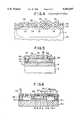
FIG. 1 shows an embodiment of a semiconductor substrate according to the present invention.
In this embodiment, a silicon oxide film (SiO2) 4 having a thickness of about 1 μm is formed on amonocrystalline silicon substrate 2. Formed on the silicon oxide film is atungsten film 5 serving as the high-melting-point metal film and having a thickness of about 800 Å. Thetungsten film 5 is patterned. Amonocrystalline silicon film 14 having a thickness of about 5000 Å is formed on thetungsten film 5.
In the embodiment shown in FIG. 2, atungsten film 5 is formed on the entire surface of asilicon oxide film 4, amonocrystalline silicon film 14 being formed on thetungsten film 5.
Instead of themonocrystalline silicon film 14 shown in FIGS. 1 and 2, a monocrystalline GaAs film may be formed.
FIGS. 3 (A) to 3 (E) illustrate a method of manufacturing the semiconductor substrate shown in FIG. 1 as well as a process for effecting element isolation while using the substrate shown in FIG. 1. FIG. 3 (A): Thereference numeral 2 indicates a monocrystalline silicon substrate whose plane orientation is (100). Asilicon oxide film 4 having a thickness of about 1 μm is formed by oxidizing the surface of the silicon substrate. Atungsten film 5 serving as the high-melting-point metal film and having a thickness of about 800 Å is deposited on thesilicon oxide film 4 by means of sputtering, etc.
Thetungsten film 5 is then patterned by means of photomechanical process and etching. Apolycrystalline silicon film 6 having a thickness of about 5000 Å is deposited on the thus patterned tungsten film by means of the LPCVD method. A silicon nitride film (Si3 N4) 8 having a thickness of about 800 Å is formed on thepolycrystalline silicon film 6 by means of the CVD method. Apolyethylene glycol layer 10 serving as the cooling medium is formed on the silicon nitride film 8, and anoptical glass plate 12 is disposed on the polyethylene glycol layer so that the thickness of the polyethylene glycol layer may become uniform, whereby the thickness of thepolyethylene glycol layer 10 is set to about 2 to 3 mm.
An argonion laser beam 13 converged by means of a lens is irradiated through theoptical glass plate 12 to thepolycrystalline silicon film 6. The molten portion 7 of thepolycrystalline silicon film 6 is shifted by moving thesilicon substrate 2 or thelaser beam 13, thereby growing thesingle crystal 14.
In the case of using a continuous-oscillation argon ion laser, the laser beam irradiation condition is such that its optical output is in the range of several W to 20 W, for example, 3 W, the laser beam diameter on thepolycrystalline silicon film 6 is in the range of 20 to 100 μm or so, and the scanning speed of the laser beam is in the range of several cm to 25 cm/sec or so. Thepolycrystalline silicon film 6 thus grows into a monocrystalline silicon film.
Thereafter, theglass plate 12, thepolyethylene glycol layer 10 and the silicon nitride film 8 are removed, and thus a semiconductor substrate is formed.
The process of forming element isolation regions will now be described referring to FIG. 3(B) to FIG. 3(E).
FIG. 3 (B): Asilicon oxide film 16 having a thickness of 250 to 500 Å is formed by thermally oxidizing the surface of themonocrystalline silicon film 14. Further, a silicon nitride film (Si3 N4) 18 having a thickness of about 1000 Å is formed on thesilicon oxide film 16 by means of the CVD method.
Next, thesilicon nitride film 18 is patterned by means of photomechanical process and etching which are the means usually adopted in patterning a silicon nitride film. Wet-etching is performed on those parts of thesilicon oxide film 16 which are exposed through the openings of thesilicon nitride film 18, until the etched portion reaches to those parts thereof which are beneath thesilicon nitride film 18.
Then, etching is performed on themonocrystalline silicon film 14 using an alkali-type anisotropic etchant. This etching progresses obliquely, along the (111) plane. This anisotropic etching is performed until the (111) plane gets laterally below the tips a, b of the eaves of thesilicon nitride film 18.
FIG. 3 (C) Next, etching is performed on themonocrystalline silicon film 14 while using thesilicon nitride film 18 as a mask, until the etching reaches thesilicon oxide film 4. This results ingrooves 20 being formed in themonocrystalline silicon film 14.
FIG. 3 (D) Selective oxidation is performed using thesilicon nitride film 18 as a mask, thereby forming thicksilicon oxide films 22 having a thickness of 0.3 to 1 μm or so in thegrooves 20. The surfaces of thegrooves 20 are thus covered with silicon oxide films.
Thereafter, thesilicon nitride film 18 used as a mask is removed.
FIG. 3 (E) A silicon nitride film 24 having a thickness of about 1000 Å is formed over the entire surface of thesilicon oxide film 16 again. This silicon nitride film 24 serves to prevent oxidation from further progressing toward the inside of themonocrystalline silicon film 14 during the subsequent oxidizing process, and to prevent crystal defects from generating in themonocrystalline silicon film 14. If, however, no strict requirements are imposed on themonocrystalline silicon film 14, the formation of this silicon nitride film 24 may be omitted.
Etching of the silicon nitride film 24 is performed in such a manner that thetungsten film 5 is exposed within thegrooves 20. Thereafter,polycrystalline silicon 26 is buried in thegrooves 20. The resistance of thispolycrystalline silicon 26 is lowered by diffusing phosphorous or the like in thepolycrystalline silicon 26.
In a substrate in which element isolation is thus effected, the potential of themonocrystalline silicon film 14 in regions which are covered with thetungsten film 5 can be equalized with the potential of thegrooves 20. For example, if themonocrystalline silicon film 14 is used as the wells for producing MOS transistors, electrical contact to these wells can be made through thegrooves 20. If, for example, bipolar transistors are made on or in themonocrystalline silicon 14, electrical contact to their collectors can be made through thegrooves 20.
When no electrical contact is to be made through thegrooves 20, thepolycrystalline silicon 26 is buried in thegrooves 20, and is oxidized to form silicon oxide film on the exposed portion of the polycrystalline silicon. This allows themonocrystalline silicon film 14 to form silicon islands which are completely isolated from thegrooves 20 and thesilicon oxide film 4 located below thetungsten film 5.
For filling up thegrooves 20 for isolation, there may be employed a dielectric material such as SiO2 or Si3 N4, or a polymeric material as well as thepolycrystalline silicon 26.
By forming on the thus formed silicon islands elements by means of the normal MOS process or bipolar process, a high-speed device having small junction capacity can be realized.
In order that thepolyethylene glycol layer 10 shown in FIG. 3(A) can be spread more uniformly, a silicon oxide film having a thickness of about 1000 Å may be formed on the silicon nitride film 8 by means of, for example, the LPCVD method, and then the silicon oxide film thus formed may be covered with thepolyethylene glycol layer 10. This is due to the fact thatpolyethylene glycol 10 tends to wet silicon oxide film better than silicon nitride film.
Theoptical glass plate 12 is provided for the purpose of making the thickness of thepolyethylene glycol layer 10 uniform, and can be omitted.
In the case of producing a semiconductor substrate in which the high-melting-point metal film is formed over the entire surface ofsilicon oxide film 4 as shown in FIG. 2, the same overall method as described with reference to FIG. 3(A) may be adopted.
Next, the method of forming a monocrystalline GaAs film on a dielectric film will be shown.
Similarly to the case shown in FIG. 3(A), asilicon oxide film 4 having a thickness of about 1 μm is formed on amonocrystalline silicon substrate 2. A GaAs film having a thickness of about 5000 Å is formed on thesilicon oxide film 4 by means of evaporation method. Thereafter, a silicon nitride film 8 is formed on the GaAs film. Formed on the silicon nitride film 8 is apolyethylene glycol layer 10 serving as the cooling medium, anoptical glass plate 12 being disposed on thepolyethylene glycol layer 10. Then, an argonion laser beam 13 is applied to the GaAs film and scanned, thereby melting the GaAs film and effecting crystal growth.
In accordance with this example, a three-layer solid state structure can be obtained in which a monocrystalline GaAs film is formed on amonocrystalline silicon substrate 2 covered with an insulatingfilm 4. For example, an element is formed on the monocrystalline silicon substrate which constitutes the lowermost layer by means of the usual MOS process or bipolar process and an optical device such as a light emitting diode or a laser diode is formed on the monocrystalline GaAs film which constitutes the uppermost layer, whereby an electronic device can be realized in which an I/O device is integrated with a peripheral circuit.
While it is difficult at present to realize a GaAs single-crystal having a large diameter, this method makes it possible to form a monocrystalline GaAs on a monocrystalline silicon substrate having a large diameter.
While, in this embodiment, a laser beam recrystallization is shown as the manufacturing method, the present invention can be applied in the same manner as in the above to cases where other types of energy such as an electron beam are employed.
In a semiconductor integrated circuit device, such as a solid state structure, MOS transistors, for example, are formed on a semiconductor substrate, such as a monocrystalline silicon substrate. Electrical contact are normally provided on the surface of the substrate on which the semiconductor elements are formed.
FIG. 4 shows, by way of example, a conventional MOS transistor structure formed by means of the LSI process.
Thereference numeral 70 indicates an N-type monocrystalline silicon substrate on which a P-well 71 is formed. Asource 72 and adrain 73 are formed in the P-well 71 by virtue of an N+ diffusion region, and agate electrode 75 is formed in the channel region through agate oxide film 74.
On the other hand, a P+ diffusion region 76 which is of the same conductivity type as the well 71 is formed to provide electrical contact to thewell 71. Thereference numeral 77 indicates a field oxide film for element isolation. Afield oxide film 77 for element isolation is also disposed between the MOS transistor and thediffusion region 76. The technical term "field" means an elements separating area excluding an active area (a transistor area). The reference numerals 78 and 79 indicate an inter-layer insulating film and a wiring of Al, an Al-Si alloy or the like.
In the case of a semiconductor device whose conductivity type is reverse to that shown in FIG. 4, that is, in a semiconductor device which includes a P-type substrate 70, an N-type well 71, a P+ -type source 72, a P+ -type drain 73, and an N+ -type diffusion region, afield oxide film 77 for element isolation is provided likewise.
Since a semiconductor device of this type requires anelement isolation region 77 between thediffusion region 76 and the semiconductor elements, the well contact portion occupies a large area, which reduces the degree of integration of the semiconductor device.
Besides, thediffusion region 76 for contacting the well has to be taken into consideration in the case of designing the circuits, which can present design impediments.
Moreover, the N-well is connected to Vcc (5 V), and the P-well or P-substrate is connected to Vss (0 V). In the case of a semiconductor integrated circuit on which a logic circuit and a memory circuit are mounted together, the characteristic of either the logic circuit or the memory circuit is impaired to some extent.
FIGS. 5 to 7 show embodiments of semiconductor devices such as a solid state structure realized by the use of the semiconductor substrate according to the present invention. Such semiconductor devices are improved in the degree of circuit integration, have circuit constitution simplified to facilitate circuit design, and exhibit a high degree of freedom with respect to the potential of the well or the substrate.
In the semiconductor devices shown in FIGS. 5 to 7, a monocrystalline silicon film is formed on an insulating foundation covered at least partly with a high-melting-point metal film or a high-melting-point metal alloy film, the monocrystalline silicon film being isolated by a groove having side walls made of dielectric films, thereby forming a well. Formed in the well is a semiconductor element, the above-mentioned high-melting-point metal film or high-melting-point metal alloy film of the well extending into the isolating groove. A conductor is buried in the groove to permit electrical contact to the well. The insulating foundation may comprise, for example, a monocrystalline silicon substrate on which a film of dielectric material such as SiO2 or Si3 N4 is formed, or may comprise a dielectric plate. The high-melting-point metal may be W, Ti, Mo, Pt, etc., and the high-melting-point metal alloy the silicide of one of the above, for example. The conductor to be buried in the groove may be a substance which is capable of coming into ohmic contact with a high-melting-point metal or an alloy of the high-melting-point metals, a low-resistance metal, or a polycrystalline or amorphous silicon with its resistance lowered by addition of suitable impurities.
The high-melting-point metal film or the high-melting-point metal alloy film below the well in which the semiconductor element is formed serves as a buried layer having a low-resistance. Since this buried layer extends into the groove of the element isolation region to thereby be connected to the conductor within the groove, electrical contact to the well can be made through the groove of the element isolation region. A diffusion region which has conventionally been necessary for making electrical contact to the well, does not exist here.
Referring to FIG. 5, thereference numeral 2 indicates a monocrystalline silicon substrate on the surface of which asilicon oxide film 4 having a thickness of 5000 to 6000 Å is formed. Atungsten film 5 having a thickness of 800 to 1000 Å is formed on thesilicon oxide fim 4 and is patterned. Asilicon film 14 having a thickness of 5000 to 8000 Å is formed on thesilicon oxide film 4 and thetungsten film 5. Themonocrystalline silicon film 14 is isolated by an element isolating groove the side surfaces of which are covered withdielectric films 30 such as silicon oxide films or silicon nitride films, aconductor 26 being buried in the groove. Theconductor 26 may, for example, be polycrystalline silicon having its resistance lowered by addition of impurities. Thetungsten film 5 extends into the element isolating groove to be in contact with theconductor 26.
Asource 34 and adrain 36 are formed by means of impurity diffusion in themonocrystalline silicon film 14 isolated by the groove. If themonocrystalline silicon film 14 is of the P-type, thesource 34 and thedrain 36 are of the N+ -type. If themonocrystalline silicon film 14 is of the N-type, thesource 34 and thedrain 36 are of the P+ -type. Agate electrode 40 is formed in the channel region through agate oxide film 38. Thereference numeral 42 indicates an inter-layer insulating film, and the reference numeral 44 a metal wiring of Al, Al-Si or the like. Theconductor 26 in the groove is also connected to ametal wiring 44.
Next, a manufacturing method for the semiconductor device shown in FIG. 5 will be described.
The process for forming amonocrystalline silicon film 14 is the same as that shown in FIG. 3(A).
That region of themonocrystalline silicon film 14 where a groove serving as the isolation region is to be formed is etched by means of RIE (Reactive Ion Etching) to form a groove. Formed on the inner walls of the groove as well as on themonocrystalline silicon film 14 is adielectric film 30 such as a silicon oxide film or a silicon nitride film. The dielectric film which is in the region for element formation is removed afterwards. If an oxide film is formed on thetungsten film 5, it is removed by RIE etching or the like which is performed for the purpose of removing the dielectric film in the region for element formation.
After the isolating groove is filled up with polycrystalline silicon containing or not containing impurities, impurities are deposited and diffused, or are injected into the polycrystalline silicon which does not contain impurities. This causes thetungsten film 5 and the low-resistance polycrystalline silicon 26 to be connected to each other in the groove.
Afterwards, a semiconductor element is formed on themonocrystalline silicon film 14 in accordance with the usual LSI process. Then, a contact is formed on top of thepolycrystalline silicon 26 buried in the isolating groove, thereby making it possible to electrically connect to themonocrystalline silicon 14.
In the embodiment shown in FIG. 6, a tungsten film 5-1 serving as a first high-melting-point metal film is formed on a silicon oxide film 4-1. A silicon oxide film 4-2 is formed and patterned on the tungsten film 5-1. Formed and patterned on the silicon oxide film 4-2 is a tungsten film 5-2 serving as a second high-melting-point metal film.
The reference numerals 14-1 and 14-2 indicate monocrystalline silicon films which are isolated from each other by element isolating grooves. Impurities are introduced into the monocrystalline silicon film regions 14-1 and 14-2, the former being of the N-type and the latter of the P-type.
A source 34P and a drain 36P are formed in each of the monocrystalline silicon film regions 14-1 by virtue of the P30 -type diffusion region. Formed in each of the monocrystalline silicon film regions 14-2 are asource 34n and adrain 36n by virtue of the N+ -type diffusion region. Agate electrode 40 is formed on each of the channel regions. Formed in the regions 14-1 are P-channel MOS transistors and, in the regions 14-2, N-channel MOS transistors.
The monocrystalline silicon film regions 14-1, 14-1 are connected to each other by the tungsten film 5-1, and are respectively connected to a power source terminal of, for example, +5 V through the polycrystalline silicon 26-1 which contains impurities and is disposed in a corresponding element isolating groove. On the other hand, each of the monocrystalline silicon film regions 14-2 is connected to a ground terminal through the tungsten film 5-2 and the polycrystalline silicon 26-2 which contains impurities and is disposed in a corresponding element isolating groove.
As in the embodiment shown in FIG. 6, the high-melting-point metal films or the high-melting-point metal alloy films 5-1 and 5-2 respectively disposed below the monocrystalline silicon film regions 14-1 and 14-2 are formed as a two-layer structure in which the dielectric film 4-2 intervenes between the metal films 5-1 and 5-2 or the metal alloy films 5-1 and 5-2, whereby electrical contacts can be made to separated wells which should be at the same potential.
In the embodiment shown in FIG. 7, a tungsten film, for example, is deposited as the high-melting-point metal film on thesilicon oxide film 4 provided in themonocrystalline silicon substrate 2, and is patterned as indicated by the reference numerals 5-3, 5-4 and 5--5. The monocrystalline silicon film formed on top of the tungsten films 5-3, 5-4, 5--5 is isolated into active area 14-3, 14-4 and 14-5, by means of LOCOS (Local Oxidation of Silicon) isolation and grooving isolation. Thereference numeral 46 indicates a field oxide film for LOCOS isolation. The reference numerals 26-3, 26-4 and 26-5 indicate polycrystalline silicon which is buried in the grooves for grooving isolation and whose resistance is lowered by adding impurities thereto. The polycrystalline silicon portions are connected in the respective grooves for isolation to the tungsten films 5-3, 5-4 and 5--5, respectively.
A desired element is formed by means of MOS process in each of the active area 14-3, 14-4 and 14-5 which are defined by isolation. The embodiment shown in FIG. 7 further includes sources 34-3, 34-4 and 34-5, drains 36-3, 36-4 and 36-5,gate electrodes 40, inter-layer insulatingfilms 42, and ametal wiring 44.
The elements formed in the respective field active area 14-3, 14-4 and 14-5 allow electrical contact to be made to the respective polycrystalline silicon portions 26-3, 26-4 and 26-5 through the respective tungsten films 5-3, 5-4 and 5--5. Accordingly, if, for example, three types of transistors are made, separate substrate potentials can be set in conformity with the respective transistors. If, for example, the three transistors are a memory transistor, an N-channel MOS transistor and a P-channel MOS transistor, substrate potentials which are optimum for the respective transistors can be set, thus making it possible to establish the optimum conditions on individual transistors. Thus, by separately setting the substrate potentials of the respective elements, a flexible circuit construction can be attained.
In the embodiment shown in FIG. 7, both the LOCOS and grooving isolation methods are applied to the isolation regions, but it is also possible to adopt the grooving method only, as in the embodiments shown in FIGS. 5 and 6.
While, in the above embodiments, a monocrystalline silicon substrate is used as thesubstrate 2, it is also possible to employ a dielectric substrate such as ceramic and to deposit a dielectric film such as a silicon oxide film on the surface of the dielectric substrate by means of the CVD method or the like.
The embodiments shown in FIGS. 5 to 7 allow the element isolating regions to be used for the purpose of making electrical contact to the well.
Accordingly, in accordance with these embodiments, there is no necessity for providing diffusion regions for making contact with the wells, which makes it possible to realize a high-density structure of the semiconductor devices.
Furthermore, since the circuit pattern is simplified, circuit design is facilitated. FIG. 8 shows a conventional semiconductor device having a structure called OST (see Japanese Patent Publication No. 62-40858). "OST construction" means a structure of transistor surrounded by oxide compound film (or substrate).
The conventional device shown in FIG. 8 includes asilicon substrate 80, afield oxide film 81, an N+ -type type buriedlayer 82, an N- -type epitaxial layer 83, abase 84, anemitter 85 and acollector contact 86.
To diminish the junction capacity and the parasitic capacity in the isolation portions isolating the transistors from each other, a groove extending through the buriedlayer 82 is formed in each isolation portion. The surface of the groove is covered with asilicon oxide film 87, the groove being filled up withpolycrystalline silicon 88. Thereference numeral 89 indicates a P+ -type channel cut. Since the transistor shown in FIG. 8 adopts N+ -TYPE diffusion regions as the buriedlayer 82, a junction capacity exists between the buriedlayer 82 and thesilicon substate 80.
In FIGS. 9 and 10, there are shown embodiments in which the present invention is applied to a conventional-type semiconductor device such as a solid state structure in order to provide a semiconductor device having a high switching speed. Such semiconductor device improved in switching speed is attained by employing as the buried layer a high-melting-point metal film (including a high-melting-point metal alloy such as a high-melting-point metal silicide) to further diminish the junction capacity and the parasitic capacity. In both drawings, the metal wiring, passivation films, etc. are omitted.
In the embodiment shown in FIG. 9, asilicon oxide film 4 having a thickness of about 1 μm is formed on asilicon substrate 2. Atungsten film 5 which serves as the high-melting-point metal film and which has a thickness of 800 to 1000 Å is formed and patterned on thesilicon oxide film 4. Amonocrystalline silicon film 14 having a thickness of about 5000 Å is formed on thetungsten film 5. Formed on themonocrystalline silicon film 14 are transistors each equipped with abase 48, anemitter 50 and acollector contact 52 utilizing themonocrystalline silicon film 14 as the collector.
Formed in each of the isolation portions is a groove reaching thesilicon oxide film 4. The surface of the groove is covered with asilicon oxide film 30, the groove being filled up withpolycrystalline silicon 26a not doped with impurities.
Eachcollector contact 52 is in contact with thetungsten film 5 which constitutes a buried layer.
Unlike the embodiment shown in FIG. 9, the embodiment shown in FIG. 10 includes nocollector contacts 52, thetungsten film 5 constituting the buried layer being exposed inside the groove in each isolation portion. Thepolycrystalline silicon 26 with which fills up the groove in the isolation portion is a polycrystalline silicon whose the resistance is lowered by doping it with impurities. Contact holes are provided over thepolycrystalline silicon 26. The contact of thetungsten film 5 with thepolycrystalline silicon 26 makes it possible to effect collector contact in the isolation portion.
In the embodiment shown in FIG. 10, the requisite area for each transistor becomes small, thereby making it possible to increase the degree of integration.
The method of manufacturing the semiconductor device shown in FIG. 9 will now be described on reference to FIG. 11 (A) to FIG. 11 (E) .
FIG. 11 (A) The method illustrated in FIG. 3 (A) is adopted in forming a monocrystalline silicon film on an insulator.
FIG. 11 (B) Next,regions 54 where the isolating portions are to be formed,regions 56 where the collector contacts are to be formed andregions 58 where the bases are to be formed are respectively masked with silicon nitride films, and thereafter afield oxide film 46 having a thickness of 1 to 1.5 μm is formed by means of selective oxidation.
FIG. 11 (C) Subsequently, asilicon nitride film 60 having a thickness of 0.1 to 0.2 μm is formed over the entire surface of thefield oxide film 46 by means of the CVD method, and a PSG (Phosphorus Silicate Glass)film 62 having a thickness of 0.5 μm or so is formed on thesilicon nitride film 60.
By means of photomechanical process and etching there are removed thesilicon nitride film 60 and thePSG film 62 existing in theregions 54 where the isolation portions are to be formed, to thereby form openings.
FIG. 11 (D) Next, theregions 54 where the isolation sections are to be formed are etched through the respective openings by means of the RIE method using (CCl4 + BCl3) gas, thereby forminggrooves 63 reaching thesilicon oxide film 4.
Afterwards, thePSG film 62 is removed by means of wet etching.
FIG. 11 (E) Then, asilicon oxide film 30 is formed by selectively oxidizing the surface of eachgroove 63, andpolycrystalline silicon 26a which is not doped with impurities is grown in eachgroove 63, so that eachgroove 63 is filled up with thepolycrystalline silicon 26a. Materials other than polycrystalline silicon, for example, insulators such as SiO2 and Si3 N4 or polymeric materials, may be employed for filling up the grooves.
The surface of thepolycrystalline silicon 26a is selectively oxidized using thesilicon nitride film 60, thereby covering the surface of thepolycrystalline silicon 26a. The silicon oxide film formed at that time is connected to thefield oxide film 46. Afterwards, thesilicon nitride film 60 is removed.
After that, bases, emitters and collector contacts are formed in accordance with the conventional bipolar process.
In the case of manufacturing the semiconductor device shown in FIG. 10, theregions 56 where the collector contacts are to be formed are not provided. Instead, patterning is so effected that thetungsten film 5 extends into theregions 54 where the isolation regions are to be formed. To lower the resistance of thepolycrystalline silicon 26 with which the grooves in the isolation regions are filled up, phosphorous is diffused in the polycrystalline silicon. In order to use thepolycrystalline silicon 26 as the collector contacts, contact holes are provided in the silicon oxide film situated above thepolycrystalline silicon 26.
In the semiconductor devices of the OST structure shown in FIGS. 9 and 10, the isolation regions are formed as insulated grooves, and a high-melting-point metal film is employed as the buried layer, so that the junction capacity and the parastic capacity can be further diminished, and the switching speed of the semiconductor device can be increased.
Claims (3)
1. A solid state structure comprising:
a foundation made of a dielectric material;
a first metal film made of an electrically conductive metal and disposed on said foundation;
a monocrystalline semiconductor film disposed on said first metal film;
a plurality of grooves formed in said monocrystalline semiconductor film so as to divide said monocrystalline semiconductor film into islands which are laterally spaced apart from each other and to reach an upper surface of said first metal film;
a plurality of first dielectric films disposed at bottoms of some of said islands such that said first dielectric films are spaced apart from each other, each of said first dielectric films overlying an upper surface of said first metal film, and extending and projecting into adjacent islands;
a plurality of second metal films each disposed on one of said first dielectric films in such a manner as to be sandwiched between said one of said first dielectric films and a selected island corresponding to each of said some of said islands, each of said second metal films extending and projecting into grooves defining said selected island;
second dielectric films disposed on side walls of respective islands defining said grooves so that said islands are electrically isolated from each other; and
a conductor material buried in each of grooves defined by said second dielectric films so that said selected island can be electrically connected to an outside of said structure through one of said second metal films, and islands other than said selected island can be electrically connected to the outside of said structure through said first metal film.
2. A solid state structure according to claim 1, in which said selected island includes an active device, and said one of said second metal films serves as an electrode for making electrical contact to said active device in said selected island.
3. A solid state structure according to claim 1, in which an island which is laterally spaced apart from said selected island comprises MOS device of a first type formed therein, and said selected island comprises MOS device of a complementary type, said structure comprising a CMOS IC.
Priority Applications (1)
| Application Number | Priority Date | Filing Date | Title |
|---|---|---|---|
| US08/458,800US5565697A (en) | 1988-06-28 | 1995-06-02 | Semiconductor structure having island forming grooves |
Applications Claiming Priority (15)
| Application Number | Priority Date | Filing Date | Title |
|---|---|---|---|
| JP63-162117 | 1988-06-28 | ||
| JP16211788 | 1988-06-28 | ||
| JP16292588 | 1988-06-29 | ||
| JP63-162925 | 1988-06-29 | ||
| JP63-171326 | 1988-07-09 | ||
| JP17132688 | 1988-07-09 | ||
| JP63-199146 | 1988-08-09 | ||
| JP19914688 | 1988-08-09 | ||
| JP1-72356 | 1989-03-23 | ||
| JP1072356AJP2750890B2 (en) | 1988-06-28 | 1989-03-23 | Semiconductor substrate manufacturing method |
| US37154389A | 1989-06-26 | 1989-06-26 | |
| US07/715,717US5173446A (en) | 1988-06-28 | 1991-06-13 | Semiconductor substrate manufacturing by recrystallization using a cooling medium |
| US97012692A | 1992-11-02 | 1992-11-02 | |
| US08/341,265US5459346A (en) | 1988-06-28 | 1994-11-17 | Semiconductor substrate with electrical contact in groove |
| US08/458,800US5565697A (en) | 1988-06-28 | 1995-06-02 | Semiconductor structure having island forming grooves |
Related Parent Applications (1)
| Application Number | Title | Priority Date | Filing Date |
|---|---|---|---|
| US08/341,265DivisionUS5459346A (en) | 1988-06-28 | 1994-11-17 | Semiconductor substrate with electrical contact in groove |
Publications (1)
| Publication Number | Publication Date |
|---|---|
| US5565697Atrue US5565697A (en) | 1996-10-15 |
Family
ID=27572640
Family Applications (2)
| Application Number | Title | Priority Date | Filing Date |
|---|---|---|---|
| US08/341,265Expired - Fee RelatedUS5459346A (en) | 1988-06-28 | 1994-11-17 | Semiconductor substrate with electrical contact in groove |
| US08/458,800Expired - Fee RelatedUS5565697A (en) | 1988-06-28 | 1995-06-02 | Semiconductor structure having island forming grooves |
Family Applications Before (1)
| Application Number | Title | Priority Date | Filing Date |
|---|---|---|---|
| US08/341,265Expired - Fee RelatedUS5459346A (en) | 1988-06-28 | 1994-11-17 | Semiconductor substrate with electrical contact in groove |
Country Status (1)
| Country | Link |
|---|---|
| US (2) | US5459346A (en) |
Cited By (91)
| Publication number | Priority date | Publication date | Assignee | Title |
|---|---|---|---|---|
| US5825067A (en)* | 1996-06-12 | 1998-10-20 | Kabushiki Kaisha Toshiba | Dielectrically isolated IC merged with surge protection circuit and method for manufacturing the same |
| US5859469A (en)* | 1997-07-18 | 1999-01-12 | Advanced Micro Devices, Inc. | Use of tungsten filled slots as ground plane in integrated circuit structure |
| US5910687A (en)* | 1997-01-24 | 1999-06-08 | Chipscale, Inc. | Wafer fabrication of die-bottom contacts for electronic devices |
| US5994738A (en)* | 1997-12-16 | 1999-11-30 | Advanced Micro Devices | Silicon oxide insulator (SOI) semiconductor having selectively linked body |
| US6037635A (en)* | 1997-01-28 | 2000-03-14 | Semiconductor Energy Laboratory Co., Ltd. | Semiconductor device with transistors formed on different layers |
| US6127733A (en)* | 1997-03-07 | 2000-10-03 | Nec Corporation | Check pattern for via-hole opening examination |
| US6127717A (en)* | 1998-06-24 | 2000-10-03 | Advanced Micro Devices | Totally self-aligned transistor with polysilicon shallow trench isolation |
| US6281551B1 (en)* | 1998-05-04 | 2001-08-28 | International Business Machines Corporation | Back-plane for semiconductor device |
| US6355950B1 (en)* | 1998-09-23 | 2002-03-12 | Intel Corporation | Substrate interconnect for power distribution on integrated circuits |
| DE10215328A1 (en)* | 2001-12-28 | 2003-07-10 | Ihp Gmbh | Isolation method for semiconductor devices used in microelectronics comprises a first switch, a second switch and a screen consisting of metal screening element for screening impurity signals between the two switches |
| US20030160233A1 (en)* | 2002-02-28 | 2003-08-28 | Rendon Michael J. | Method of forming a semiconductor device having an energy absorbing layer and structure thereof |
| US6630714B2 (en)* | 2001-12-27 | 2003-10-07 | Kabushiki Kaisha Toshiba | Semiconductor device formed in semiconductor layer arranged on substrate with one of insulating film and cavity interposed between the substrate and the semiconductor layer |
| US20040242010A1 (en)* | 2003-05-30 | 2004-12-02 | International Business Machines Corporation | Sti stress modification by nitrogen plasma treatment for improving performance in small width devices |
| US6828649B2 (en)* | 2002-05-07 | 2004-12-07 | Agere Systems Inc. | Semiconductor device having an interconnect that electrically connects a conductive material and a doped layer, and a method of manufacture therefor |
| US20040256700A1 (en)* | 2003-06-17 | 2004-12-23 | International Business Machines Corporation | High-performance CMOS devices on hybrid crystal oriented substrates |
| US20040262784A1 (en)* | 2003-06-30 | 2004-12-30 | International Business Machines Corporation | High performance cmos device structures and method of manufacture |
| US20050012174A1 (en)* | 1998-08-31 | 2005-01-20 | Kao David Y. | Selectively doped trench device isolation |
| US20050054145A1 (en)* | 2003-09-09 | 2005-03-10 | International Business Machines Corporation | Method for reduced n+ diffusion in strained si on sige substrate |
| US20050054148A1 (en)* | 2003-09-10 | 2005-03-10 | International Business Machines Corporation | METHOD AND STRUCTURE FOR IMPROVED MOSFETs USING POLY/SILICIDE GATE HEIGHT CONTROL |
| US20050059214A1 (en)* | 2003-09-16 | 2005-03-17 | International Business Machines Corporation | Method and structure of vertical strained silicon devices |
| US6869866B1 (en) | 2003-09-22 | 2005-03-22 | International Business Machines Corporation | Silicide proximity structures for CMOS device performance improvements |
| US20050064646A1 (en)* | 2003-09-23 | 2005-03-24 | Dureseti Chidambarrao | NFETs using gate induced stress modulation |
| US20050064686A1 (en)* | 2003-09-23 | 2005-03-24 | Dureseti Chidambarrao | Strained silicon on relaxed sige film with uniform misfit dislocation density |
| US20050082616A1 (en)* | 2003-10-20 | 2005-04-21 | Huajie Chen | High performance stress-enhanced MOSFETs using Si:C and SiGe epitaxial source/drain and method of manufacture |
| US20050082634A1 (en)* | 2003-10-16 | 2005-04-21 | International Business Machines Corporation | High performance strained cmos devices |
| US20050085022A1 (en)* | 2003-10-20 | 2005-04-21 | Dureseti Chidambarrao | Strained dislocation-free channels for CMOS and method of manufacture |
| US6887751B2 (en) | 2003-09-12 | 2005-05-03 | International Business Machines Corporation | MOSFET performance improvement using deformation in SOI structure |
| US20050093076A1 (en)* | 2003-11-05 | 2005-05-05 | International Business Machines Corporation | METHOD AND STRUCTURE FOR FORMING STRAINED Si FOR CMOS DEVICES |
| US20050098829A1 (en)* | 2003-11-06 | 2005-05-12 | Doris Bruce B. | High mobility CMOS circuits |
| US20050106799A1 (en)* | 2003-11-14 | 2005-05-19 | International Business Machines Corporation | Stressed semiconductor device structures having granular semiconductor material |
| US20050106790A1 (en)* | 2003-11-13 | 2005-05-19 | Kangguo Cheng | Strained silicon on a SiGe on SOI substrate |
| US20050130358A1 (en)* | 2003-12-12 | 2005-06-16 | Dureseti Chidambarrao | Strained finFETs and method of manufacture |
| US20050145954A1 (en)* | 2004-01-05 | 2005-07-07 | International Business Machines Corporation | Structures and methods for making strained mosfets |
| EP1560269A1 (en)* | 2004-01-30 | 2005-08-03 | Alcatel | MOS capacitor in an integrated semiconductor circuit |
| US20050189589A1 (en)* | 2004-02-27 | 2005-09-01 | International Business Machines Corporation | Hybrid soi/bulk semiconductor transistors |
| US20050194699A1 (en)* | 2004-03-03 | 2005-09-08 | International Business Machines Corporation | Mobility enhanced cmos devices |
| US20050269561A1 (en)* | 2004-06-03 | 2005-12-08 | Dureseti Chidambarrao | Strained Si on multiple materials for bulk or SOI substrates |
| US20050277271A1 (en)* | 2004-06-09 | 2005-12-15 | International Business Machines Corporation | RAISED STI PROCESS FOR MULTIPLE GATE OX AND SIDEWALL PROTECTION ON STRAINED Si/SGOI STRUCTURE WITH ELEVATED SOURCE/DRAIN |
| US20050285187A1 (en)* | 2004-06-24 | 2005-12-29 | International Business Machines Corporation | Strained-silicon CMOS device and method |
| US20050285192A1 (en)* | 2004-06-29 | 2005-12-29 | International Business Machines Corporation | Structures and methods for manufacturing p-type mosfet withgraded embedded silicon-germanium source-drain and/or extension |
| US20060001089A1 (en)* | 2004-07-02 | 2006-01-05 | International Business Machines Corporation | Ultra-thin, high quality strained silicon-on-insulator formed by elastic strain transfer |
| US20060019462A1 (en)* | 2004-07-23 | 2006-01-26 | International Business Machines Corporation | Patterned strained semiconductor substrate and device |
| US20060113568A1 (en)* | 2004-11-30 | 2006-06-01 | International Business Machines Corporation | Structure and method of applying stresses to pfet and nfet transistor channels for improved performance |
| US20060118912A1 (en)* | 2004-12-08 | 2006-06-08 | International Business Machines Corporation | Methodology for recovery of hot carrier induced degradation in bipolar devices |
| US20060125008A1 (en)* | 2004-12-14 | 2006-06-15 | International Business Machines Corporation | Dual stressed soi substrates |
| US20060124974A1 (en)* | 2004-12-15 | 2006-06-15 | International Business Machines Corporation | Structure and method to generate local mechanical gate stress for mosfet channel mobility modification |
| US20060151838A1 (en)* | 2005-01-12 | 2006-07-13 | International Business Machines Corporation | Enhanced pfet using shear stress |
| US20060157795A1 (en)* | 2005-01-19 | 2006-07-20 | International Business Machines Corporation | Structure and method to optimize strain in cmosfets |
| US20060157731A1 (en)* | 2002-04-29 | 2006-07-20 | Husher John D | Method of providing a CMOS output stage utilizing a buried power buss |
| US20060160317A1 (en)* | 2005-01-18 | 2006-07-20 | International Business Machines Corporation | Structure and method to enhance stress in a channel of cmos devices using a thin gate |
| US20060172495A1 (en)* | 2005-01-28 | 2006-08-03 | International Business Machines Corporation | STRUCTURE AND METHOD FOR MANUFACTURING PLANAR STRAINED Si/SiGe SUBSTRATE WITH MULTIPLE ORIENTATIONS AND DIFFERENT STRESS LEVELS |
| US20060172500A1 (en)* | 2005-02-01 | 2006-08-03 | International Business Machines Corporation | Stucture and method to induce strain in a semiconductor device channel with stressed film under the gate |
| US20060180866A1 (en)* | 2005-02-15 | 2006-08-17 | International Business Machines Corporation | Structure and method for manufacturing strained finfet |
| US7118999B2 (en) | 2004-01-16 | 2006-10-10 | International Business Machines Corporation | Method and apparatus to increase strain effect in a transistor channel |
| US20060228836A1 (en)* | 2005-04-12 | 2006-10-12 | International Business Machines Corporation | Method and structure for forming strained devices |
| US7164188B2 (en)* | 2000-12-13 | 2007-01-16 | Micron Technology, Inc. | Buried conductor patterns formed by surface transformation of empty spaces in solid state materials |
| US20070045775A1 (en)* | 2005-08-26 | 2007-03-01 | Adam Thomas N | Mobility enhancement in SiGe heterojunction bipolar transistors |
| US20070069294A1 (en)* | 2005-09-29 | 2007-03-29 | International Business Machines Corporation | Stress engineering using dual pad nitride with selective soi device architecture |
| US7202132B2 (en) | 2004-01-16 | 2007-04-10 | International Business Machines Corporation | Protecting silicon germanium sidewall with silicon for strained silicon/silicon germanium MOSFETs |
| US20070099360A1 (en)* | 2005-11-03 | 2007-05-03 | International Business Machines Corporation | Integrated circuits having strained channel field effect transistors and methods of making |
| US20070096170A1 (en)* | 2005-11-02 | 2007-05-03 | International Business Machines Corporation | Low modulus spacers for channel stress enhancement |
| US20070096206A1 (en)* | 2005-11-03 | 2007-05-03 | International Business Machines Corporation | Gate electrode stress control for finfet performance enhancement |
| US20070105299A1 (en)* | 2005-11-10 | 2007-05-10 | International Business Machines Corporation | Dual stress memory technique method and related structure |
| US7217949B2 (en) | 2004-07-01 | 2007-05-15 | International Business Machines Corporation | Strained Si MOSFET on tensile-strained SiGe-on-insulator (SGOI) |
| US20070111417A1 (en)* | 2004-08-31 | 2007-05-17 | International Business Machines Corporation | Strained-silicon cmos device and method |
| US20070108531A1 (en)* | 2005-11-14 | 2007-05-17 | International Business Machines Corporation | Rotational shear stress for charge carrier mobility modification |
| US20070108525A1 (en)* | 2005-11-14 | 2007-05-17 | International Business Machines Corporation | Structure and method to increase strain enhancement with spacerless fet and dual liner process |
| US20070120154A1 (en)* | 2005-11-30 | 2007-05-31 | International Business Machines Corporation | Finfet structure with multiply stressed gate electrode |
| US20070158753A1 (en)* | 2006-01-09 | 2007-07-12 | International Business Machines Corporation | Semiconductor device structure having low and high performance devices of same conductive type on same substrate |
| US20070158743A1 (en)* | 2006-01-11 | 2007-07-12 | International Business Machines Corporation | Thin silicon single diffusion field effect transistor for enhanced drive performance with stress film liners |
| US7247534B2 (en) | 2003-11-19 | 2007-07-24 | International Business Machines Corporation | Silicon device on Si:C-OI and SGOI and method of manufacture |
| US20070196987A1 (en)* | 2006-02-21 | 2007-08-23 | Dureseti Chidambarrao | Pseudomorphic Si/SiGe/Si body device with embedded SiGe source/drain |
| US20070202654A1 (en)* | 2006-02-28 | 2007-08-30 | International Business Machines Corporation | Spacer and process to enhance the strain in the channel with stress liner |
| US20070254422A1 (en)* | 2006-04-28 | 2007-11-01 | International Business Machines Corporation | High performance stress-enhance mosfet and method of manufacture |
| US20070254423A1 (en)* | 2006-04-28 | 2007-11-01 | International Business Machines Corporation | High performance stress-enhance mosfet and method of manufacture |
| US20070252214A1 (en)* | 2006-04-28 | 2007-11-01 | International Business Machines Corporation | Cmos structures and methods using self-aligned dual stressed layers |
| US20080001182A1 (en)* | 2006-06-29 | 2008-01-03 | International Business Machines Corporation | Improved cmos devices with stressed channel regions, and methods for fabricating the same |
| US20080057653A1 (en)* | 2006-08-30 | 2008-03-06 | International Business Machines Corporation | Method and structure for improving device performance variation in dual stress liner technology |
| US20080122025A1 (en)* | 2006-11-03 | 2008-05-29 | Freescale Semiconductor, Inc. | Electronic device including a conductive structure extending through a buried insulating layer |
| US20080121931A1 (en)* | 2006-08-30 | 2008-05-29 | International Business Machines Corporation | Semiconductor structure and method of making same |
| US20080124889A1 (en)* | 2006-11-03 | 2008-05-29 | Freescale Semiconductor, Inc. | Process of forming an electronic device including a conductive structure extending through a buried insulating layer |
| US7381609B2 (en) | 2004-01-16 | 2008-06-03 | International Business Machines Corporation | Method and structure for controlling stress in a transistor channel |
| US7388259B2 (en) | 2002-11-25 | 2008-06-17 | International Business Machines Corporation | Strained finFET CMOS device structures |
| US20080217665A1 (en)* | 2006-01-10 | 2008-09-11 | International Business Machines Corporation | Semiconductor device structure having enhanced performance fet device |
| US20080258180A1 (en)* | 2006-01-09 | 2008-10-23 | International Business Machines Corporation | Cross-section hourglass shaped channel region for charge carrier mobility modification |
| US7476580B2 (en) | 2004-04-23 | 2009-01-13 | International Business Machines Corporation | Structures and methods for manufacturing of dislocation free stressed channels in bulk silicon and SOI CMOS devices by gate stress engineering with SiGe and/or Si:C |
| US20090127626A1 (en)* | 2007-11-15 | 2009-05-21 | International Business Machines Corporation | Stress-generating shallow trench isolation structure having dual composition |
| US7790540B2 (en) | 2006-08-25 | 2010-09-07 | International Business Machines Corporation | Structure and method to use low k stress liner to reduce parasitic capacitance |
| US8115254B2 (en) | 2007-09-25 | 2012-02-14 | International Business Machines Corporation | Semiconductor-on-insulator structures including a trench containing an insulator stressor plug and method of fabricating same |
| US8598006B2 (en) | 2010-03-16 | 2013-12-03 | International Business Machines Corporation | Strain preserving ion implantation methods |
| US20130320485A1 (en)* | 2012-05-30 | 2013-12-05 | X-Fab Semiconductor Foundries Ag | Semiconductor device |
Families Citing this family (12)
| Publication number | Priority date | Publication date | Assignee | Title |
|---|---|---|---|---|
| EP0543361B1 (en) | 1991-11-20 | 2002-02-27 | Canon Kabushiki Kaisha | Method of manufacturing a semiconductor device |
| US5981316A (en)* | 1994-11-08 | 1999-11-09 | The Board Of Trustees Of The Leland Stanford Junior University | Method of fabrication of atomic chain circuit network |
| US6790714B2 (en)* | 1995-07-03 | 2004-09-14 | Sanyo Electric Co., Ltd. | Semiconductor device, display device and method of fabricating the same |
| US5771110A (en) | 1995-07-03 | 1998-06-23 | Sanyo Electric Co., Ltd. | Thin film transistor device, display device and method of fabricating the same |
| JP3532325B2 (en) | 1995-07-21 | 2004-05-31 | 株式会社東芝 | Semiconductor storage device |
| US5723380A (en)* | 1996-03-25 | 1998-03-03 | Taiwan Semiconductor Manufacturing Company, Ltd. | Method of approach to improve metal lithography and via-plug integration |
| EP0862221A4 (en)* | 1996-09-17 | 1999-06-09 | Ngk Insulators Ltd | SEMICONDUCTOR DEVICE |
| KR100248507B1 (en)* | 1997-09-04 | 2000-03-15 | 윤종용 | Soy transistor and its manufacturing method |
| JP3472742B2 (en)* | 2000-03-31 | 2003-12-02 | Necエレクトロニクス株式会社 | Semiconductor storage device |
| US6635588B1 (en)* | 2000-06-12 | 2003-10-21 | Ultratech Stepper, Inc. | Method for laser thermal processing using thermally induced reflectivity switch |
| GB0022329D0 (en)* | 2000-09-12 | 2000-10-25 | Mitel Semiconductor Ltd | Semiconductor device |
| US8034702B2 (en)* | 2007-08-16 | 2011-10-11 | Micron Technology, Inc. | Methods of forming through substrate interconnects |
Citations (52)
| Publication number | Priority date | Publication date | Assignee | Title |
|---|---|---|---|---|
| US3614558A (en)* | 1964-09-23 | 1971-10-19 | Philips Corp | Semiconductor devices with more than one semiconductor circuit element in one body |
| US3771026A (en)* | 1970-03-25 | 1973-11-06 | Hitachi Ltd | Conductive region for semiconductor device and method for making the same |
| US3941647A (en)* | 1973-03-08 | 1976-03-02 | Siemens Aktiengesellschaft | Method of producing epitaxially semiconductor layers |
| US3961997A (en)* | 1975-05-12 | 1976-06-08 | The United States Of America As Represented By The Administrator Of The National Aeronautics And Space Administration | Fabrication of polycrystalline solar cells on low-cost substrates |
| US3996095A (en)* | 1975-04-16 | 1976-12-07 | International Business Machines Corporation | Epitaxial process of forming ferrite, Fe3 O4 and γFe2 O3 thin films on special materials |
| US4059461A (en)* | 1975-12-10 | 1977-11-22 | Massachusetts Institute Of Technology | Method for improving the crystallinity of semiconductor films by laser beam scanning and the products thereof |
| US4091169A (en)* | 1975-12-18 | 1978-05-23 | International Business Machines Corporation | Silicon oxide/silicon nitride mask with improved integrity for semiconductor fabrication |
| US4180618A (en)* | 1977-07-27 | 1979-12-25 | Corning Glass Works | Thin silicon film electronic device |
| JPS5638057A (en)* | 1979-09-06 | 1981-04-13 | Ricoh Co Ltd | Electrophotographic liquid developer |
| US4292091A (en)* | 1979-02-28 | 1981-09-29 | Vlsi Technology Research Association | Method of producing semiconductor devices by selective laser irradiation and oxidation |
| US4292730A (en)* | 1980-03-12 | 1981-10-06 | Harris Corporation | Method of fabricating mesa bipolar memory cell utilizing epitaxial deposition, substrate removal and special metallization |
| EP0047140A2 (en)* | 1980-08-28 | 1982-03-10 | Xerox Corporation | Method of converting areas of semiconductor material into single crystal areas |
| EP0057135A2 (en)* | 1981-01-23 | 1982-08-04 | FAIRCHILD CAMERA & INSTRUMENT CORPORATION | Low resistance Schottky diode on polysilicon/metal-silicide |
| EP0078681A2 (en)* | 1981-10-29 | 1983-05-11 | Xerox Corporation | Method for producing single crystal semiconductor areas |
| US4396456A (en)* | 1981-12-21 | 1983-08-02 | Cook Melvin S | Method of peeling epilayers |
| US4415383A (en)* | 1982-05-10 | 1983-11-15 | Northern Telecom Limited | Method of fabricating semiconductor devices using laser annealing |
| US4437139A (en)* | 1982-12-17 | 1984-03-13 | International Business Machines Corporation | Laser annealed dielectric for dual dielectric capacitor |
| US4472729A (en)* | 1981-08-31 | 1984-09-18 | Tokyo Shibaura Denki Kabushiki Kaisha | Recrystallized three dimensional integrated circuit |
| JPS59175721A (en)* | 1983-03-25 | 1984-10-04 | Oki Electric Ind Co Ltd | Manufacture of semiconductor device |
| US4523962A (en)* | 1982-12-13 | 1985-06-18 | Mitsubishi Denki Kabushiki Kaisha | Method for fabricating monocrystalline semiconductor layer on insulating layer by laser crystallization using a grid of anti-reflection coating disposed on poly/amorphous semiconductor |
| US4545823A (en)* | 1983-11-14 | 1985-10-08 | Hewlett-Packard Company | Grain boundary confinement in silicon-on-insulator films |
| JPS6163019A (en)* | 1984-09-03 | 1986-04-01 | Nippon Telegr & Teleph Corp <Ntt> | Formation of semiconductor thin film |
| DD234529A1 (en)* | 1985-02-04 | 1986-04-02 | Mittweida Ing Hochschule | METHOD OF RE-CRYSTALLIZING SEMICONDUCTIVE LAYERS ON DIELECTRIC LAYERS |
| JPS6197964A (en)* | 1984-10-19 | 1986-05-16 | Toshiba Corp | semiconductor equipment |
| JPS61102723A (en)* | 1984-10-26 | 1986-05-21 | Fujitsu Ltd | Manufacturing method of semiconductor device |
| DE3508469A1 (en)* | 1985-03-09 | 1986-09-11 | Messerschmitt-Bölkow-Blohm GmbH, 8012 Ottobrunn | Process for patterning layer sequences applied to a transparent substrate |
| DE3620300A1 (en)* | 1985-06-18 | 1986-12-18 | Sony Corp., Tokio/Tokyo | METHOD AND DEVICE FOR PRODUCING SINGLE-CRYSTAL THIN FILMS |
| US4643950A (en)* | 1985-05-09 | 1987-02-17 | Agency Of Industrial Science And Technology | Semiconductor device |
| JPS6240858A (en)* | 1985-08-19 | 1987-02-21 | Toshiba Corp | Message waiting displaying system for private branch exchanger |
| US4659587A (en)* | 1984-10-11 | 1987-04-21 | Hitachi, Ltd. | Electroless plating process and process for producing multilayer wiring board |
| JPS62219510A (en)* | 1986-03-19 | 1987-09-26 | Fujitsu Ltd | Formation of single crystal island region |
| JPS62286283A (en)* | 1986-06-05 | 1987-12-12 | Nippon Soken Inc | Semiconductor device |
| US4717681A (en)* | 1986-05-19 | 1988-01-05 | Texas Instruments Incorporated | Method of making a heterojunction bipolar transistor with SIPOS |
| US4727047A (en)* | 1980-04-10 | 1988-02-23 | Massachusetts Institute Of Technology | Method of producing sheets of crystalline material |
| US4732801A (en)* | 1986-04-30 | 1988-03-22 | International Business Machines Corporation | Graded oxide/nitride via structure and method of fabrication therefor |
| JPS6365641A (en)* | 1986-09-05 | 1988-03-24 | Nec Corp | Semiconductor integrated circuit |
| US4752590A (en)* | 1986-08-20 | 1988-06-21 | Bell Telephone Laboratories, Incorporated | Method of producing SOI devices |
| US4794445A (en)* | 1986-07-31 | 1988-12-27 | Hitachi, Ltd. | Semiconductor device |
| US4795679A (en)* | 1985-05-22 | 1989-01-03 | North American Philips Corporation | Monocrystalline silicon layers on substrates |
| US4816421A (en)* | 1986-11-24 | 1989-03-28 | American Telephone And Telegraph Company, At&T Bell Laboratories | Method of making a heteroepitaxial structure by mesotaxy induced by buried implantation |
| US4822751A (en)* | 1986-04-02 | 1989-04-18 | Mitsubishi Denki Kabushi Kaisha | Method of producing a thin film semiconductor device |
| US4822752A (en)* | 1986-03-07 | 1989-04-18 | Agency Of Industrial Science And Technology | Process for producing single crystal semiconductor layer and semiconductor device produced by said process |
| US4826785A (en)* | 1987-01-27 | 1989-05-02 | Inmos Corporation | Metallic fuse with optically absorptive layer |
| US4847157A (en)* | 1986-08-28 | 1989-07-11 | Libbey-Owens-Ford Co. | Glass coating method and resulting article |
| US4885052A (en)* | 1987-11-13 | 1989-12-05 | Kopin Corporation | Zone-melting recrystallization process |
| US4915772A (en)* | 1986-10-01 | 1990-04-10 | Corning Incorporated | Capping layer for recrystallization process |
| US4984048A (en)* | 1987-07-10 | 1991-01-08 | Hitachi, Ltd. | Semiconductor device with buried side contact |
| US4990464A (en)* | 1988-12-30 | 1991-02-05 | North American Philips Corp. | Method of forming improved encapsulation layer |
| US5060041A (en)* | 1987-11-12 | 1991-10-22 | Ricoh Research Institute Of General Electronics | Amorphous silicon photosensor |
| US5066610A (en)* | 1987-11-20 | 1991-11-19 | Massachusetts Institute Of Technology | Capping technique for zone-melting recrystallization of insulated semiconductor films |
| US5073815A (en)* | 1989-08-30 | 1991-12-17 | Ricoh Company, Ltd. | Semiconductor substrate and method for producing the same |
| US5173446A (en)* | 1988-06-28 | 1992-12-22 | Ricoh Company, Ltd. | Semiconductor substrate manufacturing by recrystallization using a cooling medium |
Family Cites Families (1)
| Publication number | Priority date | Publication date | Assignee | Title |
|---|---|---|---|---|
| DE234529C (en)* |
- 1994
- 1994-11-17USUS08/341,265patent/US5459346A/ennot_activeExpired - Fee Related
- 1995
- 1995-06-02USUS08/458,800patent/US5565697A/ennot_activeExpired - Fee Related
Patent Citations (53)
| Publication number | Priority date | Publication date | Assignee | Title |
|---|---|---|---|---|
| US3614558A (en)* | 1964-09-23 | 1971-10-19 | Philips Corp | Semiconductor devices with more than one semiconductor circuit element in one body |
| US3771026A (en)* | 1970-03-25 | 1973-11-06 | Hitachi Ltd | Conductive region for semiconductor device and method for making the same |
| US3941647A (en)* | 1973-03-08 | 1976-03-02 | Siemens Aktiengesellschaft | Method of producing epitaxially semiconductor layers |
| US3996095A (en)* | 1975-04-16 | 1976-12-07 | International Business Machines Corporation | Epitaxial process of forming ferrite, Fe3 O4 and γFe2 O3 thin films on special materials |
| US3961997A (en)* | 1975-05-12 | 1976-06-08 | The United States Of America As Represented By The Administrator Of The National Aeronautics And Space Administration | Fabrication of polycrystalline solar cells on low-cost substrates |
| US4059461A (en)* | 1975-12-10 | 1977-11-22 | Massachusetts Institute Of Technology | Method for improving the crystallinity of semiconductor films by laser beam scanning and the products thereof |
| US4091169A (en)* | 1975-12-18 | 1978-05-23 | International Business Machines Corporation | Silicon oxide/silicon nitride mask with improved integrity for semiconductor fabrication |
| US4180618A (en)* | 1977-07-27 | 1979-12-25 | Corning Glass Works | Thin silicon film electronic device |
| US4292091A (en)* | 1979-02-28 | 1981-09-29 | Vlsi Technology Research Association | Method of producing semiconductor devices by selective laser irradiation and oxidation |
| JPS5638057A (en)* | 1979-09-06 | 1981-04-13 | Ricoh Co Ltd | Electrophotographic liquid developer |
| US4292730A (en)* | 1980-03-12 | 1981-10-06 | Harris Corporation | Method of fabricating mesa bipolar memory cell utilizing epitaxial deposition, substrate removal and special metallization |
| US4727047A (en)* | 1980-04-10 | 1988-02-23 | Massachusetts Institute Of Technology | Method of producing sheets of crystalline material |
| EP0047140A2 (en)* | 1980-08-28 | 1982-03-10 | Xerox Corporation | Method of converting areas of semiconductor material into single crystal areas |
| EP0057135A2 (en)* | 1981-01-23 | 1982-08-04 | FAIRCHILD CAMERA & INSTRUMENT CORPORATION | Low resistance Schottky diode on polysilicon/metal-silicide |
| US4472729A (en)* | 1981-08-31 | 1984-09-18 | Tokyo Shibaura Denki Kabushiki Kaisha | Recrystallized three dimensional integrated circuit |
| EP0078681A2 (en)* | 1981-10-29 | 1983-05-11 | Xerox Corporation | Method for producing single crystal semiconductor areas |
| US4396456A (en)* | 1981-12-21 | 1983-08-02 | Cook Melvin S | Method of peeling epilayers |
| US4415383A (en)* | 1982-05-10 | 1983-11-15 | Northern Telecom Limited | Method of fabricating semiconductor devices using laser annealing |
| US4523962A (en)* | 1982-12-13 | 1985-06-18 | Mitsubishi Denki Kabushiki Kaisha | Method for fabricating monocrystalline semiconductor layer on insulating layer by laser crystallization using a grid of anti-reflection coating disposed on poly/amorphous semiconductor |
| US4437139A (en)* | 1982-12-17 | 1984-03-13 | International Business Machines Corporation | Laser annealed dielectric for dual dielectric capacitor |
| JPS59175721A (en)* | 1983-03-25 | 1984-10-04 | Oki Electric Ind Co Ltd | Manufacture of semiconductor device |
| US4545823A (en)* | 1983-11-14 | 1985-10-08 | Hewlett-Packard Company | Grain boundary confinement in silicon-on-insulator films |
| JPS6163019A (en)* | 1984-09-03 | 1986-04-01 | Nippon Telegr & Teleph Corp <Ntt> | Formation of semiconductor thin film |
| US4659587A (en)* | 1984-10-11 | 1987-04-21 | Hitachi, Ltd. | Electroless plating process and process for producing multilayer wiring board |
| JPS6197964A (en)* | 1984-10-19 | 1986-05-16 | Toshiba Corp | semiconductor equipment |
| JPS61102723A (en)* | 1984-10-26 | 1986-05-21 | Fujitsu Ltd | Manufacturing method of semiconductor device |
| DD234529A1 (en)* | 1985-02-04 | 1986-04-02 | Mittweida Ing Hochschule | METHOD OF RE-CRYSTALLIZING SEMICONDUCTIVE LAYERS ON DIELECTRIC LAYERS |
| DE3508469A1 (en)* | 1985-03-09 | 1986-09-11 | Messerschmitt-Bölkow-Blohm GmbH, 8012 Ottobrunn | Process for patterning layer sequences applied to a transparent substrate |
| US4643950A (en)* | 1985-05-09 | 1987-02-17 | Agency Of Industrial Science And Technology | Semiconductor device |
| US4795679A (en)* | 1985-05-22 | 1989-01-03 | North American Philips Corporation | Monocrystalline silicon layers on substrates |
| DE3620300A1 (en)* | 1985-06-18 | 1986-12-18 | Sony Corp., Tokio/Tokyo | METHOD AND DEVICE FOR PRODUCING SINGLE-CRYSTAL THIN FILMS |
| JPS6240858A (en)* | 1985-08-19 | 1987-02-21 | Toshiba Corp | Message waiting displaying system for private branch exchanger |
| US4822752A (en)* | 1986-03-07 | 1989-04-18 | Agency Of Industrial Science And Technology | Process for producing single crystal semiconductor layer and semiconductor device produced by said process |
| JPS62219510A (en)* | 1986-03-19 | 1987-09-26 | Fujitsu Ltd | Formation of single crystal island region |
| US4822751A (en)* | 1986-04-02 | 1989-04-18 | Mitsubishi Denki Kabushi Kaisha | Method of producing a thin film semiconductor device |
| US4732801A (en)* | 1986-04-30 | 1988-03-22 | International Business Machines Corporation | Graded oxide/nitride via structure and method of fabrication therefor |
| US4717681A (en)* | 1986-05-19 | 1988-01-05 | Texas Instruments Incorporated | Method of making a heterojunction bipolar transistor with SIPOS |
| JPS62286283A (en)* | 1986-06-05 | 1987-12-12 | Nippon Soken Inc | Semiconductor device |
| US4819037A (en)* | 1986-06-05 | 1989-04-04 | Nippon Soken, Inc. | Semiconductor device |
| US4794445A (en)* | 1986-07-31 | 1988-12-27 | Hitachi, Ltd. | Semiconductor device |
| US4752590A (en)* | 1986-08-20 | 1988-06-21 | Bell Telephone Laboratories, Incorporated | Method of producing SOI devices |
| US4847157A (en)* | 1986-08-28 | 1989-07-11 | Libbey-Owens-Ford Co. | Glass coating method and resulting article |
| JPS6365641A (en)* | 1986-09-05 | 1988-03-24 | Nec Corp | Semiconductor integrated circuit |
| US4915772A (en)* | 1986-10-01 | 1990-04-10 | Corning Incorporated | Capping layer for recrystallization process |
| US4816421A (en)* | 1986-11-24 | 1989-03-28 | American Telephone And Telegraph Company, At&T Bell Laboratories | Method of making a heteroepitaxial structure by mesotaxy induced by buried implantation |
| US4826785A (en)* | 1987-01-27 | 1989-05-02 | Inmos Corporation | Metallic fuse with optically absorptive layer |
| US4984048A (en)* | 1987-07-10 | 1991-01-08 | Hitachi, Ltd. | Semiconductor device with buried side contact |
| US5060041A (en)* | 1987-11-12 | 1991-10-22 | Ricoh Research Institute Of General Electronics | Amorphous silicon photosensor |
| US4885052A (en)* | 1987-11-13 | 1989-12-05 | Kopin Corporation | Zone-melting recrystallization process |
| US5066610A (en)* | 1987-11-20 | 1991-11-19 | Massachusetts Institute Of Technology | Capping technique for zone-melting recrystallization of insulated semiconductor films |
| US5173446A (en)* | 1988-06-28 | 1992-12-22 | Ricoh Company, Ltd. | Semiconductor substrate manufacturing by recrystallization using a cooling medium |
| US4990464A (en)* | 1988-12-30 | 1991-02-05 | North American Philips Corp. | Method of forming improved encapsulation layer |
| US5073815A (en)* | 1989-08-30 | 1991-12-17 | Ricoh Company, Ltd. | Semiconductor substrate and method for producing the same |
Non-Patent Citations (11)
| Title |
|---|
| "Hand Book of SDI-Structure Forming Technology", pp. 239-249, (1987). |
| B Y. Tsaur, et al., Stress enhanced carrier mobility in zone melting recrystallized polycrystalline Si films on SiO 2 coated substrates , Appl. Phys. Lett. 40(4), Feb. 15, 1982, pp. 322 324.* |
| B-Y. Tsaur, et al., "Stress-enhanced carrier mobility in zone melting recrystallized polycrystalline Si films on SiO2 -coated substrates", Appl. Phys. Lett. 40(4), Feb. 15, 1982, pp. 322-324. |
| Hand Book of SDI Structure Forming Technology , pp. 239 249, (1987).* |
| S. A. Lyon, et al., "Microstrain in laser-crystallized silicon islands on fused silica", Appl. Phys. Lett. 40(4), Feb. 15, 1982, pp. 316-318. |
| S. A. Lyon, et al., Microstrain in laser crystallized silicon islands on fused silica , Appl. Phys. Lett. 40(4), Feb. 15, 1982, pp. 316 318.* |
| U.S. patent application Ser. No. 07/763,914 filed Sep. 23, 1991.* |
| U.S. patent application Ser. No. 07/912,894 filed Jul. 13, 1992.* |
| U.S. patent application Ser. No. 08/006,147 filed Jan. 19, 1993.* |
| W. G. Hawkins, et al., "Growth of single-crystal silicon islands on bulk fused silica by CO2 laser annealing", Appl. Phys. Lett. 40(4), Feb. 15, 1982, pp. 319-321. |
| W. G. Hawkins, et al., Growth of single crystal silicon islands on bulk fused silica by CO 2 laser annealing , Appl. Phys. Lett. 40(4), Feb. 15, 1982, pp. 319 321.* |
Cited By (269)
| Publication number | Priority date | Publication date | Assignee | Title |
|---|---|---|---|---|
| US5825067A (en)* | 1996-06-12 | 1998-10-20 | Kabushiki Kaisha Toshiba | Dielectrically isolated IC merged with surge protection circuit and method for manufacturing the same |
| US5910687A (en)* | 1997-01-24 | 1999-06-08 | Chipscale, Inc. | Wafer fabrication of die-bottom contacts for electronic devices |
| US6221751B1 (en) | 1997-01-24 | 2001-04-24 | Chipscale, Inc. | Wafer fabrication of die-bottom contacts for electronic devices |
| US6037635A (en)* | 1997-01-28 | 2000-03-14 | Semiconductor Energy Laboratory Co., Ltd. | Semiconductor device with transistors formed on different layers |
| US6127733A (en)* | 1997-03-07 | 2000-10-03 | Nec Corporation | Check pattern for via-hole opening examination |
| US5859469A (en)* | 1997-07-18 | 1999-01-12 | Advanced Micro Devices, Inc. | Use of tungsten filled slots as ground plane in integrated circuit structure |
| US5994738A (en)* | 1997-12-16 | 1999-11-30 | Advanced Micro Devices | Silicon oxide insulator (SOI) semiconductor having selectively linked body |
| US6281551B1 (en)* | 1998-05-04 | 2001-08-28 | International Business Machines Corporation | Back-plane for semiconductor device |
| US6127717A (en)* | 1998-06-24 | 2000-10-03 | Advanced Micro Devices | Totally self-aligned transistor with polysilicon shallow trench isolation |
| US7259442B2 (en)* | 1998-08-31 | 2007-08-21 | Micron Technology, Inc. | Selectively doped trench device isolation |
| US20050012174A1 (en)* | 1998-08-31 | 2005-01-20 | Kao David Y. | Selectively doped trench device isolation |
| US6355950B1 (en)* | 1998-09-23 | 2002-03-12 | Intel Corporation | Substrate interconnect for power distribution on integrated circuits |
| US6495454B2 (en) | 1998-09-23 | 2002-12-17 | Intel Corporation | Substrate interconnect for power distribution on integrated circuits |
| US7164188B2 (en)* | 2000-12-13 | 2007-01-16 | Micron Technology, Inc. | Buried conductor patterns formed by surface transformation of empty spaces in solid state materials |
| US20040026739A1 (en)* | 2001-12-27 | 2004-02-12 | Tsutomu Sato | Semiconductor device formed in semiconductor layer arranged on substrate with one of insulating film and cavity interposed between the substrate and the semiconductor layer |
| US7019365B2 (en) | 2001-12-27 | 2006-03-28 | Kabushiki Kaisha Toshiba | Semiconductor device formed in semiconductor layer arranged on substrate with one of insulating film and cavity interposed between the substrate and the semiconductor layer |
| US20050156245A1 (en)* | 2001-12-27 | 2005-07-21 | Tsutomu Sato | Semiconductor device formed in semiconductor layer arranged on substrate with one of insulating film and cavity interposed between the substrate and the semiconductor layer |
| US20080012078A1 (en)* | 2001-12-27 | 2008-01-17 | Tsutomu Sato | Semiconductor device formed in semiconductor layer arranged on substrate with one of insulating film and cavity interposed between the substrate and the semiconductor layer |
| US6630714B2 (en)* | 2001-12-27 | 2003-10-07 | Kabushiki Kaisha Toshiba | Semiconductor device formed in semiconductor layer arranged on substrate with one of insulating film and cavity interposed between the substrate and the semiconductor layer |
| US7420249B2 (en) | 2001-12-27 | 2008-09-02 | Kabushiki Kaisha Toshiba | Semiconductor device formed in semiconductor layer arranged on substrate with one of insulating film and cavity interposed between the substrate and the semiconductor layer |
| DE10215328A1 (en)* | 2001-12-28 | 2003-07-10 | Ihp Gmbh | Isolation method for semiconductor devices used in microelectronics comprises a first switch, a second switch and a screen consisting of metal screening element for screening impurity signals between the two switches |
| US20030160233A1 (en)* | 2002-02-28 | 2003-08-28 | Rendon Michael J. | Method of forming a semiconductor device having an energy absorbing layer and structure thereof |
| US7102167B1 (en)* | 2002-04-29 | 2006-09-05 | Micrel, Inc. | Method and system for providing a CMOS output stage utilizing a buried power buss |
| US20060157731A1 (en)* | 2002-04-29 | 2006-07-20 | Husher John D | Method of providing a CMOS output stage utilizing a buried power buss |
| US6828649B2 (en)* | 2002-05-07 | 2004-12-07 | Agere Systems Inc. | Semiconductor device having an interconnect that electrically connects a conductive material and a doped layer, and a method of manufacture therefor |
| US7388259B2 (en) | 2002-11-25 | 2008-06-17 | International Business Machines Corporation | Strained finFET CMOS device structures |
| US6887798B2 (en) | 2003-05-30 | 2005-05-03 | International Business Machines Corporation | STI stress modification by nitrogen plasma treatment for improving performance in small width devices |
| US20040242010A1 (en)* | 2003-05-30 | 2004-12-02 | International Business Machines Corporation | Sti stress modification by nitrogen plasma treatment for improving performance in small width devices |
| US7479688B2 (en) | 2003-05-30 | 2009-01-20 | International Business Machines Corporation | STI stress modification by nitrogen plasma treatment for improving performance in small width devices |
| US20040238914A1 (en)* | 2003-05-30 | 2004-12-02 | International Business Machines Corporation | STI stress modification by nitrogen plasma treatment for improving performance in small width devices |
| US20040256700A1 (en)* | 2003-06-17 | 2004-12-23 | International Business Machines Corporation | High-performance CMOS devices on hybrid crystal oriented substrates |
| US7713807B2 (en) | 2003-06-17 | 2010-05-11 | International Business Machines Corporation | High-performance CMOS SOI devices on hybrid crystal-oriented substrates |
| US7329923B2 (en) | 2003-06-17 | 2008-02-12 | International Business Machines Corporation | High-performance CMOS devices on hybrid crystal oriented substrates |
| US20080096330A1 (en)* | 2003-06-17 | 2008-04-24 | International Business Machines Corporation | High-performance cmos soi devices on hybrid crystal-oriented substrates |
| US7436029B2 (en) | 2003-06-30 | 2008-10-14 | International Business Machines Corporation | High performance CMOS device structures and method of manufacture |
| US20080026522A1 (en)* | 2003-06-30 | 2008-01-31 | International Business Machines Corporation | High performance cmos device structures and method of manufacture |
| US7279746B2 (en) | 2003-06-30 | 2007-10-09 | International Business Machines Corporation | High performance CMOS device structures and method of manufacture |
| US20040262784A1 (en)* | 2003-06-30 | 2004-12-30 | International Business Machines Corporation | High performance cmos device structures and method of manufacture |
| US20050054145A1 (en)* | 2003-09-09 | 2005-03-10 | International Business Machines Corporation | Method for reduced n+ diffusion in strained si on sige substrate |
| US7410846B2 (en) | 2003-09-09 | 2008-08-12 | International Business Machines Corporation | Method for reduced N+ diffusion in strained Si on SiGe substrate |
| US7345329B2 (en) | 2003-09-09 | 2008-03-18 | International Business Machines Corporation | Method for reduced N+ diffusion in strained Si on SiGe substrate |
| US20050145992A1 (en)* | 2003-09-09 | 2005-07-07 | Dureseti Chidambarrao | Method for reduced N+ diffusion in strained Si on SiGe substrate |
| US7297601B2 (en) | 2003-09-09 | 2007-11-20 | International Business Machines Corporation | Method for reduced N+ diffusion in strained Si on SiGe substrate |
| US20050145950A1 (en)* | 2003-09-10 | 2005-07-07 | Dureseti Chidambarrao | Method and structure for improved MOSFETs using poly/silicide gate height control |
| US7091563B2 (en) | 2003-09-10 | 2006-08-15 | International Business Machines Corporation | Method and structure for improved MOSFETs using poly/silicide gate height control |
| US6890808B2 (en) | 2003-09-10 | 2005-05-10 | International Business Machines Corporation | Method and structure for improved MOSFETs using poly/silicide gate height control |
| US20050054148A1 (en)* | 2003-09-10 | 2005-03-10 | International Business Machines Corporation | METHOD AND STRUCTURE FOR IMPROVED MOSFETs USING POLY/SILICIDE GATE HEIGHT CONTROL |
| US20050142788A1 (en)* | 2003-09-12 | 2005-06-30 | Dureseti Chidambarrao | MOSFET performance improvement using deformation in SOI structure |
| US7745277B2 (en) | 2003-09-12 | 2010-06-29 | International Business Machines Corporation | MOSFET performance improvement using deformation in SOI structure |
| US6887751B2 (en) | 2003-09-12 | 2005-05-03 | International Business Machines Corporation | MOSFET performance improvement using deformation in SOI structure |
| US20050059214A1 (en)* | 2003-09-16 | 2005-03-17 | International Business Machines Corporation | Method and structure of vertical strained silicon devices |
| US7170126B2 (en) | 2003-09-16 | 2007-01-30 | International Business Machines Corporation | Structure of vertical strained silicon devices |
| US6869866B1 (en) | 2003-09-22 | 2005-03-22 | International Business Machines Corporation | Silicide proximity structures for CMOS device performance improvements |
| US20050064687A1 (en)* | 2003-09-22 | 2005-03-24 | International Business Machines Corporation | Silicide proximity structures for cmos device performance improvements |
| US20050064686A1 (en)* | 2003-09-23 | 2005-03-24 | Dureseti Chidambarrao | Strained silicon on relaxed sige film with uniform misfit dislocation density |
| US7964865B2 (en) | 2003-09-23 | 2011-06-21 | International Business Machines Corporation | Strained silicon on relaxed sige film with uniform misfit dislocation density |
| US6872641B1 (en) | 2003-09-23 | 2005-03-29 | International Business Machines Corporation | Strained silicon on relaxed sige film with uniform misfit dislocation density |
| US20050064646A1 (en)* | 2003-09-23 | 2005-03-24 | Dureseti Chidambarrao | NFETs using gate induced stress modulation |
| US7144767B2 (en) | 2003-09-23 | 2006-12-05 | International Business Machines Corporation | NFETs using gate induced stress modulation |
| US20050164477A1 (en)* | 2003-09-23 | 2005-07-28 | Dureseti Chidambarrao | Strained silicon on relaxed sige film with uniform misfit dislocation density |
| US20060270136A1 (en)* | 2003-10-16 | 2006-11-30 | International Business Machines Corporation | High performance strained cmos devices |
| US20050082634A1 (en)* | 2003-10-16 | 2005-04-21 | International Business Machines Corporation | High performance strained cmos devices |
| US7847358B2 (en) | 2003-10-16 | 2010-12-07 | International Business Machines Corporation | High performance strained CMOS devices |
| US7119403B2 (en) | 2003-10-16 | 2006-10-10 | International Business Machines Corporation | High performance strained CMOS devices |
| US7303949B2 (en) | 2003-10-20 | 2007-12-04 | International Business Machines Corporation | High performance stress-enhanced MOSFETs using Si:C and SiGe epitaxial source/drain and method of manufacture |
| US9023698B2 (en) | 2003-10-20 | 2015-05-05 | Samsung Electronics Co., Ltd. | High performance stress-enhanced MOSFETs using Si:C and SiGe epitaxial source/drain and method of manufacture |
| US8901566B2 (en) | 2003-10-20 | 2014-12-02 | International Business Machines Corporation | High performance stress-enhanced MOSFETs using Si:C and SiGe epitaxial source/drain and method of manufacture |
| US7037770B2 (en) | 2003-10-20 | 2006-05-02 | International Business Machines Corporation | Method of manufacturing strained dislocation-free channels for CMOS |
| US7495291B2 (en) | 2003-10-20 | 2009-02-24 | International Business Machines Corporation | Strained dislocation-free channels for CMOS and method of manufacture |
| US20050139930A1 (en)* | 2003-10-20 | 2005-06-30 | Dureseti Chidambarrao | Strained dislocation-free channels for CMOS and method of manufacture |
| US20070264783A1 (en)* | 2003-10-20 | 2007-11-15 | International Business Machines Corporation | High performance stress-enhanced mosfets using si:c and sige epitaxial source/drain and method of manufacture |
| US8168489B2 (en) | 2003-10-20 | 2012-05-01 | International Business Machines Corporation | High performance stress-enhanced MOSFETS using Si:C and SiGe epitaxial source/drain and method of manufacture |
| US9401424B2 (en) | 2003-10-20 | 2016-07-26 | Samsung Electronics Co., Ltd. | High performance stress-enhanced MOSFETs using Si:C and SiGe epitaxial source/drain and method of manufacture |
| US20050082616A1 (en)* | 2003-10-20 | 2005-04-21 | Huajie Chen | High performance stress-enhanced MOSFETs using Si:C and SiGe epitaxial source/drain and method of manufacture |
| US20050085022A1 (en)* | 2003-10-20 | 2005-04-21 | Dureseti Chidambarrao | Strained dislocation-free channels for CMOS and method of manufacture |
| US20070020806A1 (en)* | 2003-11-05 | 2007-01-25 | International Business Machines Corporation | Method and structure for forming strained si for cmos devices |
| US7700951B2 (en) | 2003-11-05 | 2010-04-20 | International Business Machines Corporation | Method and structure for forming strained Si for CMOS devices |
| US20080283824A1 (en)* | 2003-11-05 | 2008-11-20 | International Business Machines Corporation, | Method and structure for forming strained si for cmos devices |
| US20100109048A1 (en)* | 2003-11-05 | 2010-05-06 | International Business Machines Corporation | Method and structure for forming strained si for cmos devices |
| US20080003735A1 (en)* | 2003-11-05 | 2008-01-03 | International Business Machines Corporation | Method and structure for forming strained si for cmos devices |
| US7429752B2 (en) | 2003-11-05 | 2008-09-30 | International Business Machines Corporation | Method and structure for forming strained SI for CMOS devices |
| US7550338B2 (en) | 2003-11-05 | 2009-06-23 | International Business Machines Corporation | Method and structure for forming strained SI for CMOS devices |
| US7928443B2 (en) | 2003-11-05 | 2011-04-19 | International Business Machines Corporation | Method and structure for forming strained SI for CMOS devices |
| US7129126B2 (en) | 2003-11-05 | 2006-10-31 | International Business Machines Corporation | Method and structure for forming strained Si for CMOS devices |
| US20050093076A1 (en)* | 2003-11-05 | 2005-05-05 | International Business Machines Corporation | METHOD AND STRUCTURE FOR FORMING STRAINED Si FOR CMOS DEVICES |
| US20050098829A1 (en)* | 2003-11-06 | 2005-05-12 | Doris Bruce B. | High mobility CMOS circuits |
| US20080237720A1 (en)* | 2003-11-06 | 2008-10-02 | International Business Machines Corporation | High mobility cmos circuits |
| US8013392B2 (en) | 2003-11-06 | 2011-09-06 | International Business Machines Corporation | High mobility CMOS circuits |
| US7015082B2 (en) | 2003-11-06 | 2006-03-21 | International Business Machines Corporation | High mobility CMOS circuits |
| US20060027868A1 (en)* | 2003-11-06 | 2006-02-09 | Ibm Corporation | High mobility CMOS circuits |
| US7285826B2 (en) | 2003-11-06 | 2007-10-23 | International Business Machines Corporation | High mobility CMOS circuits |
| US7468538B2 (en) | 2003-11-13 | 2008-12-23 | International Business Machines Corporation | Strained silicon on a SiGe on SOI substrate |
| US20050106790A1 (en)* | 2003-11-13 | 2005-05-19 | Kangguo Cheng | Strained silicon on a SiGe on SOI substrate |
| US7029964B2 (en) | 2003-11-13 | 2006-04-18 | International Business Machines Corporation | Method of manufacturing a strained silicon on a SiGe on SOI substrate |
| US7488658B2 (en) | 2003-11-14 | 2009-02-10 | International Business Machines Corporation | Stressed semiconductor device structures having granular semiconductor material |
| US20080064172A1 (en)* | 2003-11-14 | 2008-03-13 | International Business Machines Corporation | Stressed semiconductor device structures having granular semiconductor material |
| US20050106799A1 (en)* | 2003-11-14 | 2005-05-19 | International Business Machines Corporation | Stressed semiconductor device structures having granular semiconductor material |
| US7122849B2 (en) | 2003-11-14 | 2006-10-17 | International Business Machines Corporation | Stressed semiconductor device structures having granular semiconductor material |
| US8232153B2 (en) | 2003-11-19 | 2012-07-31 | International Business Machines Corporation | Silicon device on Si:C-OI and SGOI and method of manufacture |
| US8633071B2 (en) | 2003-11-19 | 2014-01-21 | International Business Machines Corporation | Silicon device on Si: C-oi and Sgoi and method of manufacture |
| US8119472B2 (en) | 2003-11-19 | 2012-02-21 | International Business Machines Corporation | Silicon device on Si:C SOI and SiGe and method of manufacture |
| US9040373B2 (en) | 2003-11-19 | 2015-05-26 | International Business Machines Corporation | Silicon device on SI:C-OI and SGOI and method of manufacture |
| US7247534B2 (en) | 2003-11-19 | 2007-07-24 | International Business Machines Corporation | Silicon device on Si:C-OI and SGOI and method of manufacture |
| US20050130358A1 (en)* | 2003-12-12 | 2005-06-16 | Dureseti Chidambarrao | Strained finFETs and method of manufacture |
| US7198995B2 (en) | 2003-12-12 | 2007-04-03 | International Business Machines Corporation | Strained finFETs and method of manufacture |
| US7749842B2 (en) | 2004-01-05 | 2010-07-06 | International Business Machines Corporation | Structures and methods for making strained MOSFETs |
| US20070218620A1 (en)* | 2004-01-05 | 2007-09-20 | International Business Machines Corporation | Structures and methods for making strained mosfets |
| US20050145954A1 (en)* | 2004-01-05 | 2005-07-07 | International Business Machines Corporation | Structures and methods for making strained mosfets |
| US7247912B2 (en) | 2004-01-05 | 2007-07-24 | International Business Machines Corporation | Structures and methods for making strained MOSFETs |
| US20060281272A1 (en)* | 2004-01-16 | 2006-12-14 | International Business Machines Corporation | Method and apparatus for increase strain effect in a transistor channel |
| US7790558B2 (en) | 2004-01-16 | 2010-09-07 | International Business Machines Corporation | Method and apparatus for increase strain effect in a transistor channel |
| US7498602B2 (en) | 2004-01-16 | 2009-03-03 | International Business Machines Corporation | Protecting silicon germanium sidewall with silicon for strained silicon/silicon mosfets |
| US7202132B2 (en) | 2004-01-16 | 2007-04-10 | International Business Machines Corporation | Protecting silicon germanium sidewall with silicon for strained silicon/silicon germanium MOSFETs |
| US7462915B2 (en) | 2004-01-16 | 2008-12-09 | International Business Machines Corporation | Method and apparatus for increase strain effect in a transistor channel |
| US7381609B2 (en) | 2004-01-16 | 2008-06-03 | International Business Machines Corporation | Method and structure for controlling stress in a transistor channel |
| US7118999B2 (en) | 2004-01-16 | 2006-10-10 | International Business Machines Corporation | Method and apparatus to increase strain effect in a transistor channel |
| EP1560269A1 (en)* | 2004-01-30 | 2005-08-03 | Alcatel | MOS capacitor in an integrated semiconductor circuit |
| US7767503B2 (en) | 2004-02-27 | 2010-08-03 | International Business Machines Corporation | Hybrid SOI/bulk semiconductor transistors |
| US7923782B2 (en) | 2004-02-27 | 2011-04-12 | International Business Machines Corporation | Hybrid SOI/bulk semiconductor transistors |
| US20080090366A1 (en)* | 2004-02-27 | 2008-04-17 | Huilong Zhu | Hybrid SOI-Bulk Semiconductor Transistors |
| US20050189589A1 (en)* | 2004-02-27 | 2005-09-01 | International Business Machines Corporation | Hybrid soi/bulk semiconductor transistors |
| US7452761B2 (en) | 2004-02-27 | 2008-11-18 | International Business Machines Corporation | Hybrid SOI-bulk semiconductor transistors |
| US20050194699A1 (en)* | 2004-03-03 | 2005-09-08 | International Business Machines Corporation | Mobility enhanced cmos devices |
| US20060148147A1 (en)* | 2004-03-03 | 2006-07-06 | Ibm | Mobility enhanced CMOS devices |
| US7205206B2 (en) | 2004-03-03 | 2007-04-17 | International Business Machines Corporation | Method of fabricating mobility enhanced CMOS devices |
| US7569848B2 (en) | 2004-03-03 | 2009-08-04 | International Business Machines Corporation | Mobility enhanced CMOS devices |
| US7476580B2 (en) | 2004-04-23 | 2009-01-13 | International Business Machines Corporation | Structures and methods for manufacturing of dislocation free stressed channels in bulk silicon and SOI CMOS devices by gate stress engineering with SiGe and/or Si:C |
| US20090149010A1 (en)* | 2004-04-23 | 2009-06-11 | International Business Machines Corporation | STRUCTURES AND METHODS FOR MANUFACTURING OF DISLOCATION FREE STRESSED CHANNELS IN BULK SILICON AND SOI MOS DEVICES BY GATE STRESS ENGINEERING WITH SiGe AND/OR Si:C |
| US7504693B2 (en) | 2004-04-23 | 2009-03-17 | International Business Machines Corporation | Dislocation free stressed channels in bulk silicon and SOI CMOS devices by gate stress engineering |
| US7713806B2 (en) | 2004-04-23 | 2010-05-11 | International Business Machines Corporation | Structures and methods for manufacturing of dislocation free stressed channels in bulk silicon and SOI MOS devices by gate stress engineering with SiGe and/or Si:C |
| US20050269561A1 (en)* | 2004-06-03 | 2005-12-08 | Dureseti Chidambarrao | Strained Si on multiple materials for bulk or SOI substrates |
| US7560328B2 (en) | 2004-06-03 | 2009-07-14 | International Business Machines Corporation | Strained Si on multiple materials for bulk or SOI substrates |
| US20070166897A1 (en)* | 2004-06-03 | 2007-07-19 | International Business Machines Corporation | STRAINED Si ON MULTIPLE MATERIALS FOR BULK OR SOI SUBSTRATES |
| US7223994B2 (en) | 2004-06-03 | 2007-05-29 | International Business Machines Corporation | Strained Si on multiple materials for bulk or SOI substrates |
| US20050277271A1 (en)* | 2004-06-09 | 2005-12-15 | International Business Machines Corporation | RAISED STI PROCESS FOR MULTIPLE GATE OX AND SIDEWALL PROTECTION ON STRAINED Si/SGOI STRUCTURE WITH ELEVATED SOURCE/DRAIN |
| US7737502B2 (en) | 2004-06-09 | 2010-06-15 | International Business Machines Corporation | Raised STI process for multiple gate ox and sidewall protection on strained Si/SGOI sructure with elevated source/drain |
| US7037794B2 (en) | 2004-06-09 | 2006-05-02 | International Business Machines Corporation | Raised STI process for multiple gate ox and sidewall protection on strained Si/SGOI structure with elevated source/drain |
| US20060128111A1 (en)* | 2004-06-09 | 2006-06-15 | International Business Machines Corporation | Raised sti process for multiple gate ox and sidewall protection on strained Si/SGOI structure with elevated source/drain |
| US7227205B2 (en) | 2004-06-24 | 2007-06-05 | International Business Machines Corporation | Strained-silicon CMOS device and method |
| US20050285187A1 (en)* | 2004-06-24 | 2005-12-29 | International Business Machines Corporation | Strained-silicon CMOS device and method |
| US20100244139A1 (en)* | 2004-06-24 | 2010-09-30 | International Business Machines Corporation | Strained-silicon cmos device and method |
| US7288443B2 (en) | 2004-06-29 | 2007-10-30 | International Business Machines Corporation | Structures and methods for manufacturing p-type MOSFET with graded embedded silicon-germanium source-drain and/or extension |
| US20050285192A1 (en)* | 2004-06-29 | 2005-12-29 | International Business Machines Corporation | Structures and methods for manufacturing p-type mosfet withgraded embedded silicon-germanium source-drain and/or extension |
| US7217949B2 (en) | 2004-07-01 | 2007-05-15 | International Business Machines Corporation | Strained Si MOSFET on tensile-strained SiGe-on-insulator (SGOI) |
| US8017499B2 (en) | 2004-07-01 | 2011-09-13 | International Business Machines Corporation | Strained Si MOSFET on tensile-strained SiGe-on-insulator (SGOI) |
| US20070155130A1 (en)* | 2004-07-01 | 2007-07-05 | International Business Machines Corporation | STRAINED Si MOSFET ON TENSILE-STRAINED SiGe-ON-INSULATOR (SGOI) |
| US20080220588A1 (en)* | 2004-07-01 | 2008-09-11 | International Business Machines Corporation | STRAINED Si MOSFET ON TENSILE-STRAINED SiGe-ON-INSULATOR (SGOI) |
| US7507989B2 (en) | 2004-07-01 | 2009-03-24 | International Business Machines Corporation | Strained Si MOSFET on tensile-strained SiGe-on-insulator (SGOI) |
| US7485518B2 (en) | 2004-07-01 | 2009-02-03 | International Business Machines Corporation | Strained Si MOSFET on tensile-strained SiGe-on-insulator (SGOI) |
| US20080042166A1 (en)* | 2004-07-01 | 2008-02-21 | International Business Machines Corporation | STRAINED Si MOSFET ON TENSILE-STRAINED SiGe-ON-INSULATOR (SGOI) |
| US20060001089A1 (en)* | 2004-07-02 | 2006-01-05 | International Business Machines Corporation | Ultra-thin, high quality strained silicon-on-insulator formed by elastic strain transfer |
| US20060081837A1 (en)* | 2004-07-02 | 2006-04-20 | International Business Machines Corporation | Ultra-thin, high quality strained silicon-on-insulator formed by elastic strain transfer |
| US7442993B2 (en) | 2004-07-02 | 2008-10-28 | International Business Machines Corporation | Ultra-thin, high quality strained silicon-on-insulator formed by elastic strain transfer |
| US6991998B2 (en) | 2004-07-02 | 2006-01-31 | International Business Machines Corporation | Ultra-thin, high quality strained silicon-on-insulator formed by elastic strain transfer |
| US20080061317A1 (en)* | 2004-07-23 | 2008-03-13 | International Business Machines Corporation | Patterned strained semiconductor substrate and device |
| US9515140B2 (en) | 2004-07-23 | 2016-12-06 | Globalfoundries Inc. | Patterned strained semiconductor substrate and device |
| US9053970B2 (en) | 2004-07-23 | 2015-06-09 | International Business Machines Corporation | Patterned strained semiconductor substrate and device |
| US20060019462A1 (en)* | 2004-07-23 | 2006-01-26 | International Business Machines Corporation | Patterned strained semiconductor substrate and device |
| US7682859B2 (en) | 2004-07-23 | 2010-03-23 | International Business Machines Corporation | Patterned strained semiconductor substrate and device |
| US7384829B2 (en) | 2004-07-23 | 2008-06-10 | International Business Machines Corporation | Patterned strained semiconductor substrate and device |
| US20070111417A1 (en)* | 2004-08-31 | 2007-05-17 | International Business Machines Corporation | Strained-silicon cmos device and method |
| US7808081B2 (en) | 2004-08-31 | 2010-10-05 | International Business Machines Corporation | Strained-silicon CMOS device and method |
| US20060113568A1 (en)* | 2004-11-30 | 2006-06-01 | International Business Machines Corporation | Structure and method of applying stresses to pfet and nfet transistor channels for improved performance |
| US7193254B2 (en) | 2004-11-30 | 2007-03-20 | International Business Machines Corporation | Structure and method of applying stresses to PFET and NFET transistor channels for improved performance |
| US20060118912A1 (en)* | 2004-12-08 | 2006-06-08 | International Business Machines Corporation | Methodology for recovery of hot carrier induced degradation in bipolar devices |
| US7723824B2 (en) | 2004-12-08 | 2010-05-25 | International Business Machines Corporation | Methodology for recovery of hot carrier induced degradation in bipolar devices |
| US7238565B2 (en) | 2004-12-08 | 2007-07-03 | International Business Machines Corporation | Methodology for recovery of hot carrier induced degradation in bipolar devices |
| US20060125008A1 (en)* | 2004-12-14 | 2006-06-15 | International Business Machines Corporation | Dual stressed soi substrates |
| US7312134B2 (en) | 2004-12-14 | 2007-12-25 | International Business Machines Corporation | Dual stressed SOI substrates |
| US20070202639A1 (en)* | 2004-12-14 | 2007-08-30 | International Business Machines Corporation | Dual stressed soi substrates |
| US7262087B2 (en) | 2004-12-14 | 2007-08-28 | International Business Machines Corporation | Dual stressed SOI substrates |
| US20070111421A1 (en)* | 2004-12-15 | 2007-05-17 | International Business Machines Corporation | Structure and method to generate local mechanical gate stress for mosfet channel mobility modification |
| US7314789B2 (en) | 2004-12-15 | 2008-01-01 | International Business Machines Corporation | Structure and method to generate local mechanical gate stress for MOSFET channel mobility modification |
| US20060124974A1 (en)* | 2004-12-15 | 2006-06-15 | International Business Machines Corporation | Structure and method to generate local mechanical gate stress for mosfet channel mobility modification |
| US7173312B2 (en) | 2004-12-15 | 2007-02-06 | International Business Machines Corporation | Structure and method to generate local mechanical gate stress for MOSFET channel mobility modification |
| US20060151838A1 (en)* | 2005-01-12 | 2006-07-13 | International Business Machines Corporation | Enhanced pfet using shear stress |
| US7274084B2 (en) | 2005-01-12 | 2007-09-25 | International Business Machines Corporation | Enhanced PFET using shear stress |
| US20060160317A1 (en)* | 2005-01-18 | 2006-07-20 | International Business Machines Corporation | Structure and method to enhance stress in a channel of cmos devices using a thin gate |
| US20080251853A1 (en)* | 2005-01-19 | 2008-10-16 | International Business Machines Corporation | STRUCTURE AND METHOD TO OPTIMIZE STRAIN IN CMOSFETs |
| US7432553B2 (en) | 2005-01-19 | 2008-10-07 | International Business Machines Corporation | Structure and method to optimize strain in CMOSFETs |
| US20060157795A1 (en)* | 2005-01-19 | 2006-07-20 | International Business Machines Corporation | Structure and method to optimize strain in cmosfets |
| US20080070357A1 (en)* | 2005-01-19 | 2008-03-20 | International Business Machines Corporation | STRUCTURE AND METHOD TO OPTIMIZE STRAIN IN CMOSFETs |
| US20070170507A1 (en)* | 2005-01-28 | 2007-07-26 | International Business Machines Corporation | STRUCTURE AND METHOD FOR MANUFACTURING PLANAR STRAINED Si/SiGe SUBSTRATE WITH MULTIPLE ORIENTATIONS AND DIFFERENT STRESS LEVELS |
| US7220626B2 (en) | 2005-01-28 | 2007-05-22 | International Business Machines Corporation | Structure and method for manufacturing planar strained Si/SiGe substrate with multiple orientations and different stress levels |
| US20060172495A1 (en)* | 2005-01-28 | 2006-08-03 | International Business Machines Corporation | STRUCTURE AND METHOD FOR MANUFACTURING PLANAR STRAINED Si/SiGe SUBSTRATE WITH MULTIPLE ORIENTATIONS AND DIFFERENT STRESS LEVELS |
| US20060172500A1 (en)* | 2005-02-01 | 2006-08-03 | International Business Machines Corporation | Stucture and method to induce strain in a semiconductor device channel with stressed film under the gate |
| US20070187773A1 (en)* | 2005-02-01 | 2007-08-16 | International Business Machines Corporation | Structure and method to induce strain in a semiconductor device channel with stressed film under the gate |
| US7256081B2 (en) | 2005-02-01 | 2007-08-14 | International Business Machines Corporation | Structure and method to induce strain in a semiconductor device channel with stressed film under the gate |
| US7314802B2 (en) | 2005-02-15 | 2008-01-01 | International Business Machines Corporation | Structure and method for manufacturing strained FINFET |
| US20070122984A1 (en)* | 2005-02-15 | 2007-05-31 | International Business Machines Corporation | Structure and method for manufacturing strained finfet |
| US7224033B2 (en) | 2005-02-15 | 2007-05-29 | International Business Machines Corporation | Structure and method for manufacturing strained FINFET |
| US20060180866A1 (en)* | 2005-02-15 | 2006-08-17 | International Business Machines Corporation | Structure and method for manufacturing strained finfet |
| US20060228836A1 (en)* | 2005-04-12 | 2006-10-12 | International Business Machines Corporation | Method and structure for forming strained devices |
| US7545004B2 (en) | 2005-04-12 | 2009-06-09 | International Business Machines Corporation | Method and structure for forming strained devices |
| US20090224286A1 (en)* | 2005-08-26 | 2009-09-10 | International Business Machines Corporation | MOBILITY ENHANCEMENT IN SiGe HETEROJUNCTION BIPOLAR TRANSISTORS |
| US20070045775A1 (en)* | 2005-08-26 | 2007-03-01 | Adam Thomas N | Mobility enhancement in SiGe heterojunction bipolar transistors |
| US7544577B2 (en) | 2005-08-26 | 2009-06-09 | International Business Machines Corporation | Mobility enhancement in SiGe heterojunction bipolar transistors |
| US7202513B1 (en) | 2005-09-29 | 2007-04-10 | International Business Machines Corporation | Stress engineering using dual pad nitride with selective SOI device architecture |
| US20070069294A1 (en)* | 2005-09-29 | 2007-03-29 | International Business Machines Corporation | Stress engineering using dual pad nitride with selective soi device architecture |
| US20070122965A1 (en)* | 2005-09-29 | 2007-05-31 | International Business Machines Corporation | Stress engineering using dual pad nitride with selective soi device architecture |
| US7550364B2 (en) | 2005-09-29 | 2009-06-23 | International Business Machines Corporation | Stress engineering using dual pad nitride with selective SOI device architecture |
| US20070096170A1 (en)* | 2005-11-02 | 2007-05-03 | International Business Machines Corporation | Low modulus spacers for channel stress enhancement |
| US7960801B2 (en) | 2005-11-03 | 2011-06-14 | International Business Machines Corporation | Gate electrode stress control for finFET performance enhancement description |
| US20070099360A1 (en)* | 2005-11-03 | 2007-05-03 | International Business Machines Corporation | Integrated circuits having strained channel field effect transistors and methods of making |
| US20070096206A1 (en)* | 2005-11-03 | 2007-05-03 | International Business Machines Corporation | Gate electrode stress control for finfet performance enhancement |
| US7655511B2 (en) | 2005-11-03 | 2010-02-02 | International Business Machines Corporation | Gate electrode stress control for finFET performance enhancement |
| US7785950B2 (en) | 2005-11-10 | 2010-08-31 | International Business Machines Corporation | Dual stress memory technique method and related structure |
| US20070105299A1 (en)* | 2005-11-10 | 2007-05-10 | International Business Machines Corporation | Dual stress memory technique method and related structure |
| US20100187636A1 (en)* | 2005-11-14 | 2010-07-29 | International Business Machines Corporation | Method to increase strain enhancement with spacerless fet and dual liner process |
| US20080105953A1 (en)* | 2005-11-14 | 2008-05-08 | International Business Machines Corporation | Rotational shear stress for charge carrier mobility modification |
| US7504697B2 (en) | 2005-11-14 | 2009-03-17 | International Business Machines | Rotational shear stress for charge carrier mobility modification |
| US7348638B2 (en) | 2005-11-14 | 2008-03-25 | International Business Machines Corporation | Rotational shear stress for charge carrier mobility modification |
| US20070108525A1 (en)* | 2005-11-14 | 2007-05-17 | International Business Machines Corporation | Structure and method to increase strain enhancement with spacerless fet and dual liner process |
| US20070108531A1 (en)* | 2005-11-14 | 2007-05-17 | International Business Machines Corporation | Rotational shear stress for charge carrier mobility modification |
| US7709317B2 (en) | 2005-11-14 | 2010-05-04 | International Business Machines Corporation | Method to increase strain enhancement with spacerless FET and dual liner process |
| US20090280626A1 (en)* | 2005-11-30 | 2009-11-12 | International Business Machines Corporation | Finfet structure with multiply stressed gate electrode |
| US7564081B2 (en) | 2005-11-30 | 2009-07-21 | International Business Machines Corporation | finFET structure with multiply stressed gate electrode |
| US20070120154A1 (en)* | 2005-11-30 | 2007-05-31 | International Business Machines Corporation | Finfet structure with multiply stressed gate electrode |
| US8058157B2 (en) | 2005-11-30 | 2011-11-15 | International Business Machines Corporation | FinFET structure with multiply stressed gate electrode |
| US20070158753A1 (en)* | 2006-01-09 | 2007-07-12 | International Business Machines Corporation | Semiconductor device structure having low and high performance devices of same conductive type on same substrate |
| US7863197B2 (en) | 2006-01-09 | 2011-01-04 | International Business Machines Corporation | Method of forming a cross-section hourglass shaped channel region for charge carrier mobility modification |
| US20080258180A1 (en)* | 2006-01-09 | 2008-10-23 | International Business Machines Corporation | Cross-section hourglass shaped channel region for charge carrier mobility modification |
| US7776695B2 (en) | 2006-01-09 | 2010-08-17 | International Business Machines Corporation | Semiconductor device structure having low and high performance devices of same conductive type on same substrate |
| US7635620B2 (en) | 2006-01-10 | 2009-12-22 | International Business Machines Corporation | Semiconductor device structure having enhanced performance FET device |
| US20080217665A1 (en)* | 2006-01-10 | 2008-09-11 | International Business Machines Corporation | Semiconductor device structure having enhanced performance fet device |
| US20100096673A1 (en)* | 2006-01-10 | 2010-04-22 | International Business Machines Corporation | Semiconductor device structure having enhanced performance fet device |
| US7935993B2 (en) | 2006-01-10 | 2011-05-03 | International Business Machines Corporation | Semiconductor device structure having enhanced performance FET device |
| US20090305471A1 (en)* | 2006-01-11 | 2009-12-10 | International Business Machines Corporation | Thin silicon single diffusion field effect transistor for enhanced drive performance with stress film liners |
| US20070158743A1 (en)* | 2006-01-11 | 2007-07-12 | International Business Machines Corporation | Thin silicon single diffusion field effect transistor for enhanced drive performance with stress film liners |
| US7691698B2 (en) | 2006-02-21 | 2010-04-06 | International Business Machines Corporation | Pseudomorphic Si/SiGe/Si body device with embedded SiGe source/drain |
| US8168971B2 (en) | 2006-02-21 | 2012-05-01 | International Business Machines Corporation | Pseudomorphic Si/SiGe/Si body device with embedded SiGe source/drain |
| US20070196987A1 (en)* | 2006-02-21 | 2007-08-23 | Dureseti Chidambarrao | Pseudomorphic Si/SiGe/Si body device with embedded SiGe source/drain |
| US8461009B2 (en) | 2006-02-28 | 2013-06-11 | International Business Machines Corporation | Spacer and process to enhance the strain in the channel with stress liner |
| US20070202654A1 (en)* | 2006-02-28 | 2007-08-30 | International Business Machines Corporation | Spacer and process to enhance the strain in the channel with stress liner |
| US20100013024A1 (en)* | 2006-04-28 | 2010-01-21 | International Business Machines Corporation | High performance stress-enhance mosfet and method of manufacture |
| US20070252214A1 (en)* | 2006-04-28 | 2007-11-01 | International Business Machines Corporation | Cmos structures and methods using self-aligned dual stressed layers |
| US7608489B2 (en) | 2006-04-28 | 2009-10-27 | International Business Machines Corporation | High performance stress-enhance MOSFET and method of manufacture |
| US20070254423A1 (en)* | 2006-04-28 | 2007-11-01 | International Business Machines Corporation | High performance stress-enhance mosfet and method of manufacture |
| US20070254422A1 (en)* | 2006-04-28 | 2007-11-01 | International Business Machines Corporation | High performance stress-enhance mosfet and method of manufacture |
| US8901662B2 (en) | 2006-04-28 | 2014-12-02 | International Business Machines Corporation | CMOS structures and methods for improving yield |
| US20070252230A1 (en)* | 2006-04-28 | 2007-11-01 | International Business Machines Corporation | Cmos structures and methods for improving yield |
| US7791144B2 (en) | 2006-04-28 | 2010-09-07 | International Business Machines Corporation | High performance stress-enhance MOSFET and method of manufacture |
| US7615418B2 (en) | 2006-04-28 | 2009-11-10 | International Business Machines Corporation | High performance stress-enhance MOSFET and method of manufacture |
| US20090194819A1 (en)* | 2006-04-28 | 2009-08-06 | International Business Machines Corporation | Cmos structures and methods using self-aligned dual stressed layers |
| US9318344B2 (en) | 2006-04-28 | 2016-04-19 | International Business Machines Corporation | CMOS structures and methods for improving yield |
| US7521307B2 (en) | 2006-04-28 | 2009-04-21 | International Business Machines Corporation | CMOS structures and methods using self-aligned dual stressed layers |
| US8853746B2 (en) | 2006-06-29 | 2014-10-07 | International Business Machines Corporation | CMOS devices with stressed channel regions, and methods for fabricating the same |
| US20080001182A1 (en)* | 2006-06-29 | 2008-01-03 | International Business Machines Corporation | Improved cmos devices with stressed channel regions, and methods for fabricating the same |
| US7790540B2 (en) | 2006-08-25 | 2010-09-07 | International Business Machines Corporation | Structure and method to use low k stress liner to reduce parasitic capacitance |
| US8754446B2 (en) | 2006-08-30 | 2014-06-17 | International Business Machines Corporation | Semiconductor structure having undercut-gate-oxide gate stack enclosed by protective barrier material |
| US7843024B2 (en) | 2006-08-30 | 2010-11-30 | International Business Machines Corporation | Method and structure for improving device performance variation in dual stress liner technology |
| US7462522B2 (en) | 2006-08-30 | 2008-12-09 | International Business Machines Corporation | Method and structure for improving device performance variation in dual stress liner technology |
| US20080121931A1 (en)* | 2006-08-30 | 2008-05-29 | International Business Machines Corporation | Semiconductor structure and method of making same |
| US20080057653A1 (en)* | 2006-08-30 | 2008-03-06 | International Business Machines Corporation | Method and structure for improving device performance variation in dual stress liner technology |
| US7491623B2 (en) | 2006-08-30 | 2009-02-17 | International Business Machines Corporation | Method of making a semiconductor structure |
| US20080122025A1 (en)* | 2006-11-03 | 2008-05-29 | Freescale Semiconductor, Inc. | Electronic device including a conductive structure extending through a buried insulating layer |
| US8188543B2 (en)* | 2006-11-03 | 2012-05-29 | Freescale Semiconductor, Inc. | Electronic device including a conductive structure extending through a buried insulating layer |
| US20080124889A1 (en)* | 2006-11-03 | 2008-05-29 | Freescale Semiconductor, Inc. | Process of forming an electronic device including a conductive structure extending through a buried insulating layer |
| US7820519B2 (en) | 2006-11-03 | 2010-10-26 | Freescale Semiconductor, Inc. | Process of forming an electronic device including a conductive structure extending through a buried insulating layer |
| US8115254B2 (en) | 2007-09-25 | 2012-02-14 | International Business Machines Corporation | Semiconductor-on-insulator structures including a trench containing an insulator stressor plug and method of fabricating same |
| US8629501B2 (en) | 2007-09-25 | 2014-01-14 | International Business Machines Corporation | Stress-generating structure for semiconductor-on-insulator devices |
| US9305999B2 (en) | 2007-09-25 | 2016-04-05 | Globalfoundries Inc. | Stress-generating structure for semiconductor-on-insulator devices |
| US9013001B2 (en) | 2007-11-15 | 2015-04-21 | International Business Machines Corporation | Stress-generating shallow trench isolation structure having dual composition |
| US8728905B2 (en) | 2007-11-15 | 2014-05-20 | International Business Machines Corporation | Stress-generating shallow trench isolation structure having dual composition |
| US8492846B2 (en) | 2007-11-15 | 2013-07-23 | International Business Machines Corporation | Stress-generating shallow trench isolation structure having dual composition |
| US20090127626A1 (en)* | 2007-11-15 | 2009-05-21 | International Business Machines Corporation | Stress-generating shallow trench isolation structure having dual composition |
| US8598006B2 (en) | 2010-03-16 | 2013-12-03 | International Business Machines Corporation | Strain preserving ion implantation methods |
| US20130320485A1 (en)* | 2012-05-30 | 2013-12-05 | X-Fab Semiconductor Foundries Ag | Semiconductor device |
| US10529866B2 (en)* | 2012-05-30 | 2020-01-07 | X-Fab Semiconductor Foundries Gmbh | Semiconductor device |
Also Published As
| Publication number | Publication date |
|---|---|
| US5459346A (en) | 1995-10-17 |
Similar Documents
| Publication | Publication Date | Title |
|---|---|---|
| US5565697A (en) | Semiconductor structure having island forming grooves | |
| US5173446A (en) | Semiconductor substrate manufacturing by recrystallization using a cooling medium | |
| US4651408A (en) | Fabrication of stacked MOS devices utilizing lateral seeding and a plurality of separate implants at different energies | |
| US5241211A (en) | Semiconductor device | |
| US5011788A (en) | Process of manufacturing semiconductor integrated circuit device and product formed thereby | |
| US4523369A (en) | Method for manufacturing a semiconductor device | |
| US4879584A (en) | Semiconductor device with isolation between MOSFET and control circuit | |
| US7259048B2 (en) | Vertical replacement-gate silicon-on-insulator transistor | |
| US4907063A (en) | Semiconductor body, and device formed therefrom, having grooves with silicon nitride on the groove surfaces | |
| KR100227766B1 (en) | Semiconductor device and the manufacturing method thereof | |
| US4992389A (en) | Making a self aligned semiconductor device | |
| US6432799B1 (en) | Method of manufacturing semiconductor integrated circuit device | |
| EP0013508B1 (en) | Semiconductor device and a method of producing the same | |
| US5049521A (en) | Method for forming dielectrically isolated semiconductor devices with contact to the wafer substrate | |
| US5073815A (en) | Semiconductor substrate and method for producing the same | |
| US6365448B2 (en) | Structure and method for gated lateral bipolar transistors | |
| US4404737A (en) | Method for manufacturing a semiconductor integrated circuit utilizing polycrystalline silicon deposition, oxidation and etching | |
| JPH06105765B2 (en) | Process of creating a semiconductor ROM array | |
| US5345102A (en) | Bipolar transistor having collector electrode penetrating emitter and base regions | |
| US4999691A (en) | Integrated circuit with stacked MOS field effect transistors | |
| US5227319A (en) | Method of manufacturing a semiconductor device | |
| US4695856A (en) | Semiconductor device | |
| JP2750890B2 (en) | Semiconductor substrate manufacturing method | |
| US5501992A (en) | Method of manufacturing bipolar transistor having ring-shaped emitter and base | |
| JP2509708B2 (en) | SOI type semiconductor device and manufacturing method thereof |
Legal Events
| Date | Code | Title | Description |
|---|---|---|---|
| FEPP | Fee payment procedure | Free format text:PAYOR NUMBER ASSIGNED (ORIGINAL EVENT CODE: ASPN); ENTITY STATUS OF PATENT OWNER: LARGE ENTITY | |
| REMI | Maintenance fee reminder mailed | ||
| LAPS | Lapse for failure to pay maintenance fees | ||
| FP | Lapsed due to failure to pay maintenance fee | Effective date:20001015 | |
| STCH | Information on status: patent discontinuation | Free format text:PATENT EXPIRED DUE TO NONPAYMENT OF MAINTENANCE FEES UNDER 37 CFR 1.362 |