US5562516A - Field-emitter fabrication using charged-particle tracks - Google Patents
Field-emitter fabrication using charged-particle tracksDownload PDFInfo
- Publication number
- US5562516A US5562516AUS08/447,470US44747095AUS5562516AUS 5562516 AUS5562516 AUS 5562516AUS 44747095 AUS44747095 AUS 44747095AUS 5562516 AUS5562516 AUS 5562516A
- Authority
- US
- United States
- Prior art keywords
- layer
- insulating layer
- electron
- gate
- conductive region
- Prior art date
- Legal status (The legal status is an assumption and is not a legal conclusion. Google has not performed a legal analysis and makes no representation as to the accuracy of the status listed.)
- Expired - Lifetime
Links
Images


Classifications
- H—ELECTRICITY
- H01—ELECTRIC ELEMENTS
- H01J—ELECTRIC DISCHARGE TUBES OR DISCHARGE LAMPS
- H01J1/00—Details of electrodes, of magnetic control means, of screens, or of the mounting or spacing thereof, common to two or more basic types of discharge tubes or lamps
- H01J1/02—Main electrodes
- H01J1/30—Cold cathodes, e.g. field-emissive cathode
- H01J1/304—Field-emissive cathodes
- H01J1/3042—Field-emissive cathodes microengineered, e.g. Spindt-type
- B—PERFORMING OPERATIONS; TRANSPORTING
- B82—NANOTECHNOLOGY
- B82Y—SPECIFIC USES OR APPLICATIONS OF NANOSTRUCTURES; MEASUREMENT OR ANALYSIS OF NANOSTRUCTURES; MANUFACTURE OR TREATMENT OF NANOSTRUCTURES
- B82Y10/00—Nanotechnology for information processing, storage or transmission, e.g. quantum computing or single electron logic
- H—ELECTRICITY
- H01—ELECTRIC ELEMENTS
- H01J—ELECTRIC DISCHARGE TUBES OR DISCHARGE LAMPS
- H01J3/00—Details of electron-optical or ion-optical arrangements or of ion traps common to two or more basic types of discharge tubes or lamps
- H01J3/02—Electron guns
- H01J3/021—Electron guns using a field emission, photo emission, or secondary emission electron source
- H01J3/022—Electron guns using a field emission, photo emission, or secondary emission electron source with microengineered cathode, e.g. Spindt-type
- H—ELECTRICITY
- H01—ELECTRIC ELEMENTS
- H01J—ELECTRIC DISCHARGE TUBES OR DISCHARGE LAMPS
- H01J9/00—Apparatus or processes specially adapted for the manufacture, installation, removal, maintenance of electric discharge tubes, discharge lamps, or parts thereof; Recovery of material from discharge tubes or lamps
- H01J9/02—Manufacture of electrodes or electrode systems
- H01J9/022—Manufacture of electrodes or electrode systems of cold cathodes
- H01J9/025—Manufacture of electrodes or electrode systems of cold cathodes of field emission cathodes
- H—ELECTRICITY
- H01—ELECTRIC ELEMENTS
- H01J—ELECTRIC DISCHARGE TUBES OR DISCHARGE LAMPS
- H01J2201/00—Electrodes common to discharge tubes
- H01J2201/30—Cold cathodes
- H01J2201/304—Field emission cathodes
- H01J2201/30403—Field emission cathodes characterised by the emitter shape
- H—ELECTRICITY
- H01—ELECTRIC ELEMENTS
- H01J—ELECTRIC DISCHARGE TUBES OR DISCHARGE LAMPS
- H01J2201/00—Electrodes common to discharge tubes
- H01J2201/30—Cold cathodes
- H01J2201/304—Field emission cathodes
- H01J2201/30446—Field emission cathodes characterised by the emitter material
- H01J2201/30453—Carbon types
- H01J2201/30457—Diamond
- H—ELECTRICITY
- H01—ELECTRIC ELEMENTS
- H01J—ELECTRIC DISCHARGE TUBES OR DISCHARGE LAMPS
- H01J2201/00—Electrodes common to discharge tubes
- H01J2201/30—Cold cathodes
- H01J2201/319—Circuit elements associated with the emitters by direct integration
Definitions
- This inventionrelates to electron-emitting devices. More particularly, this invention relates to structures and manufacturing techniques for field-emission devices (or field emitters) suitable for products such as cathode-ray tubes of the flat-panel type.
- a field-emission cathodeis an electronic device that emits electrons when subjected to an electric field of sufficient strength.
- the electric fieldis created by applying a voltage between the cathode and an electrode, typically referred to as the anode or gate electrode, situated a short distance away from the cathode.
- a field emittertypically contains a group, often a very large group, of individual electron-emissive elements distributed across a supporting structure. This configuration is commonly referred to as an area field emitter. A variety of different shapes have been investigated for the electron-emissive elements in area field emitters.
- a screen having an appropriate array of circular or square openingsis placed above the substrate electrode.
- a depositionis then performed simultaneously from two sources.
- One of the sourcesconsists of an emitter-forming metal, such as molybdenum, atoms of which are deposited in a direction perpendicular to the substrate electrode.
- the other sourceconsists of a closure material, such as a molybdenum-alumina composite. Atoms of the closure material are caused to impinge on the screen at a small angle to the substrate. The closure material progressively closes the openings in the screen as the emitter-forming metal passes through the openings to create the electron-emissive elements.
- the resultis that the emitter-forming metal is deposited in the shape of cones or pyramids depending on whether the screen openings are circular or square.
- Yoshida et alU.S. Pat. No. 5,164,632 discloses a gated field-emission structure in which solid elongated gold electron-emissive elements are situated in pores extending through an alumina layer. An address line lying under the alumina layer contacts the lower ends of the electron-emissive elements. Their upper ends are pointed. A gate electrode situated above the electron-emissive elements extends slightly into the pores.
- Yoshida et alanodically oxidize part of an aluminum plate to create a thin alumina layer having pores that extend nearly all the way through the alumina.
- An electrolytic techniqueis used to fill the pores with gold for the electron-emissive elements.
- the address lineis formed over the filled pores along the alumina side of the structure after which the remaining aluminum and part of the adjoining alumina are removed along the opposite side of the structure to re-expose the gold in the pores.
- Part of the re-exposed goldis removed during an ion-milling process utilized to sharpen the electron-emissive elements.
- Goldis then evaporatively deposited onto the alumina and partly into the pores to form the gate electrode.
- Greene et alU.S. Pat. No. 5,150,192, discloses a gated field emitter in which hollow elongated electron-emissive elements extend through a thin electrically insulating substrate.
- the electron-emissive elementshave pointed tips that protrude into cavities provided along the upper substrate surface below the gate electrode.
- a metal filmlies along the lower substrate surface.
- Greene et alcreate openings partway through the substrate by etching through a mask formed on the bottom of the substrate. Metal is deposited along the walls of the openings and along the lower substrate surface. A portion of the thickness of the substrate is removed along the upper surface. The gate electrode is then formed by a deposition/planarization procedure. The cavities are provided along the upper substrate surface after which the hollow metal portions in the openings are sharpened to complete the electron-emissive elements.
- a large-area field emitter for an application such as a flat-panel television screen where the diagonal screen dimension is 25 cmneeds a relatively strong substrate for supporting the field-emission components extending across the large emitter area.
- the requisite substrate thicknessis typically several hundred microns to 10 mm or more. Due to the ways in which Yoshida et al and Greene et al manufacture their field emitters, it would be quite difficult to attach those emitters to substrates of such thickness. Consequently, Yoshida et al and Greene et al are not suited for scaling up to large-area field-emission applications.
- Busta"Vacuum Microelectronics-1992,” J. Micromech. Microeng., Vol. 2, 1992 pp. 43-74, provides a general review of field-emission devices. Among other things, Busta discusses Utsumi, “Keynote Address, Vacuum Microelectronics: What's New and Exciting," IEEE Trans. Elect. Dev., October 1990, pp. 2276-2283, who suggests that a filament with a rounded end is the best shape for a field-emission element. Busta also discusses Betsui, "Fabrication and Characteristics of Si Field Emitter Arrays," Tech Dig IVMC 91, 1991 pp.
- the present inventionfurnishes a simple, accurate, and easily controllable process for manufacturing an efficient, reliable gated area field-emission structure.
- the inventionuses charged-particle tracks in providing the field-emitter with small electron-emissive elements self-aligned to the gate electrode.
- Each electron-emissive elementcan be formed as a pedestal having a pointed tip, as a cone, or as a combination of a pedestal and an overlying cone whose base diameter is greater than the diameter of the pedestal.
- a structureis initially created in which an electrically insulating layer lies over a lower electrically conductive region, an electrically conductive gate layer lies over the insulating layer, and a further layer lies over the gate layer.
- a multiplicity of charged-particle tracksare formed through the further layer by appropriately subjecting the structure to charged particles.
- the further layeris etched along the charged-particle tracks to create corresponding apertures through the further layer.
- the gate layeris etched through the apertures in the further layer to form corresponding gate openings through the gate layer.
- an insulating layeris etched through the gate openings to create corresponding dielectric open spaces through the insulating layer.
- this etching stepis done along charged-particle tracks which are formed through the insulating layer when the structure is subjected to the charged particles and which are respectively in line with the charged-particle tracks through the further layer.
- a like multiplicity of electron-emissive elementsare then formed over the lower conductive region in such a way that each electron-emissive element contacts the lower conductive region through a corresponding one of the dielectric open spaces.
- Each electron-emissive elementis normally centered in its dielectric open space. This is typically accomplished by creating the electron-emissive elements in such a manner that they laterally adjoin the insulating layer along the dielectric open spaces or by depositing electrically conductive material into the dielectric open spaces in a centered manner to form the electron-emissive elements even though the deposited material does not laterally adjoin the insulating layer.
- the gate layeris normally used as an etch mask so that each dielectric open space is centered on the corresponding gate opening. Consequently, the electron-emissive elements are self-aligned to the gate openings.
- each electron-emissive elementcontains a highly resistive portion and an overlying electron-emissive portion.
- the highly resistive portionsact as current limiters for preventing failure due to arcing or short circuits.
- the highly resistive portionsalso improve the emission uniformity.
- the inventionhas many advantages. For example, by using charged-particle tracks to achieve self-alignment, the electron-emissive elements and gate openings can be made quite small without regard to conventional lithographic patterning tolerances. In particular, the components of the field-emission structure can be manufactured at lateral dimensions on the nanometer scale. Because use of charged-particle tracks provides essentially infinite depth of focus, it is not necessary that the patterned surfaces be extremely flat.
- the fabrication process of the inventionis simple and highly accurate.
- the processis inexpensive and well-suited for scaling up to manufacturing large-area field emitters for cathode-ray tubes in flat-panel televisions.
- the inventionprovides a substantial advance over the prior art.
- FIGS. 1a, 1b, 1c, 1d, 1e, 1f, 1g, 1h, 1i, and 1jare cross-sectional front views representing steps in manufacturing a gated field emitter according to the invention.
- FIGS. 2a, 2b, 2c, 2d, 2e, 2f, 2g, 2h, 2i, and 2jare plan views respectively corresponding to FIGS. 1a-1j.
- the cross sections of FIGS. 1a-1jare taken through stepped plane 1--1 in FIGS. 2a-2j.
- FIGS. 3a, 3b, 3c, 3d, and 3eare cross-sectional front views representing an alternative set of steps performable on the structure of FIG. 1i for manufacturing a gated field emitter according to the invention.
- FIGS. 4a and 4bare respective expanded cross-sectional front views of one of the electron-emissive elements in FIGS. 3c and 3e.
- FIGS. 5a, 5b, 5c, 5d, and 5eare cross-sectional front structural views representing a further set of steps performable on the structure of FIG. 1i for manufacturing a gated field emitter according to the invention.
- FIG. 6is an expanded cross-sectional front view of one of the electron-emissive elements in FIG. 5c.
- FIGS. 7a, 7b, 7c, 7d, 7e, 7f, 7g, and 7hare cross-sectional front structural views representing an alternative set of steps performable on the structure of FIG. 1f for manufacturing a gated field emitter according to the invention.
- FIGS. 8a, 8b, 8c, 8d, 8e, 8f, 8g, and 8hare cross-sectional front structural views representing steps in manufacturing a gated field emitter according to the invention.
- FIGS. 9a, 9b, 9c, 9d, and 9eare cross-sectional front structural views representing a further set of steps performable on the structure of FIG. 1f for manufacturing a gated field emitter according to the invention.
- FIGS. 10a, 10b, 10c, 10d, and 10eare plan views respectively corresponding to FIGS. 9a-9e. The cross-sections of FIGS. 9a-9e are taken through plane 9--9 in FIGS. 10a-10e.
- FIG. 11is a cross-sectional front structural view depicting how the initial structure of FIG. 1a appears when the lower conductive region consists of a highly conductive part and a highly resistive part.
- FIG. 12is a cross-sectional side structural view corresponding to FIG. 11.
- the cross section of FIG. 11is taken through plane 11--11 in FIG. 12.
- the cross section of FIG. 12is taken through plane 12--12 in FIG. 11.
- FIGS. 13.1, 13.2, 13.3, and 13.4are cross-sectional front structural views respectively depicting how the final structures of FIGS. 1j, 3e, 7h, and 9e appear when they contain the two-part lower conductive region of FIG. 11.
- FIGS. 14a, 14b, 14c, 14d, 14e, 14f, 14g, 14h, 14i, 14j, 14k, and 14lare cross-sectional front structural views representing steps in manufacturing a gated field emitter that incorporates a focusing electrode according to the invention.
- FIGS. 15a, 15b, 15c, and 15dare cross-sectional front structural views representing an alternative set of steps performable on the structure of FIG. 14g for manufacturing a gated field emitter that incorporates a focusing electrode according to the invention.
- FIGS. 16a, 16b, 16c, 16d, and 16eare cross-sectional front structural views representing an alternative set of steps performable on the structure of FIG. 14f for manufacturing a gated field emitter that incorporates a focusing electrode according to the invention.
- FIGS. 17.1 and 17.2are expanded cross-sectional front views of alternative electron-emissive elements employable in the present field emitters where each electron-emissive element consists of a highly resistive portion and an overlying electron-emissive portion.
- FIGS. 18.1 and 18.2are expanded cross-sectional front views of alternative shapes for electron-emissive cones in the present field emitters.
- FIGS. 19.1, 19.2, 19.3 and 19.4are cross-sectional longitudinal views of differently shaped electron-emissive filaments usable in the field-emission structures of FIGS. 1j and 14l.
- FIG. 20is a functional diagram for the components of an electrochemical deposition system used in the invention.
- the present inventionmakes use of electrochemical deposition in which a material, usually a metal, is deposited from an (ionized) electrolyte in a (liquid) solvent. Electrochemical deposition is typically performed by passing current between a pair of electrodes to enable the material to accumulate on one of the electrodes. Nonetheless, electrochemical deposition can be performed in an electroless manner at zero applied potential.
- FIGS. 1a-1j(collectively “FIG. 1") and FIGS. 2a-2j (collectively “FIG. 2”) illustrate a process for manufacturing a gated area field-emission cathode structure according to the teachings of the invention.
- the field-emission structureis typically used to excite phosphors on a face plate in a cathode-ray tube of a flat-panel television screen.
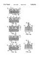
- the starting point for the fabrication processis an electrically insulating substrate 20 typically consisting of ceramic or glass.
- Substrate 20is typically configured as a plate having a largely flat upper surface and a largely flat lower surface substantially parallel to the upper surface.
- Substrate 20furnishes support for the field-emission structure.
- the substrate thicknessis at least 500 microns.
- the substrate thicknessis typically 4-14 mm. If support struts are placed between the phosphor-coated face plate and the field emitter, the substrate thickness is typically 1-2 mm.
- a lower electrically conductive region 22is formed along the top of substrate 20 as indicated in FIGS. 1a and 2a.
- Lower conductive region 22consists of a metal such as chromium. In this case, the thickness of region 22 is 0.05-1.5 micron.
- Other candidates for region 22include tantalum, tungsten, and molybdenum.
- Lower conductive region 22is typically a patterned layer containing a group of parallel lines, of which two such lines are depicted in FIG. 2a.
- region 22is configured in this way, the final field-emission structure is particularly suitable for selectively exciting phosphors in a flat-panel television.
- These linesare typically 300 microns wide for the 25-cm monochrome flat-panel television example. Nonetheless, region 22 can be arranged in various other patterns, or can even be unpatterned.
- a largely homogeneous electrically insulating layer 24is formed on the top of the structure. See FIGS. 1b and 2b. Parts of insulating layer 24 are situated on both substrate 20 and lower conductive region 22. The thickness of layer 24 is 0.1-2.0 microns, typically 1.0 micron. Suitable materials for insulating layer 24 fall into three groups: (a) organic polymers such as polycarbonate, polystyrene, and cellulose acetate, (b) inorganic glasses such as phosphate, silicate, and soda-lime glasses, and (c) crystals such as mica and quartz.
- organic polymerssuch as polycarbonate, polystyrene, and cellulose acetate
- inorganic glassessuch as phosphate, silicate, and soda-lime glasses
- crystalssuch as mica and quartz.
- a blanket electrically conductive layer 46which later becomes the gate electrode, is formed on top of insulating layer 24 as indicated in FIG. 1b.
- Conductive layer 46is typically 0.05 micron in thickness.
- Layer 46consists of a metal such as molybdenum, copper, or aluminum. The method for creating layer 46 is not particularly critical as long as its thickness is relatively uniform. Layer 46 is typically formed by a physical vapor deposition technique.
- a further electrically insulating layer 48is formed on top of conductive layer 46. Again see FIG. 1b. Insulating layer 48 is in the range of 0.2-0.5 micron in thickness. As with insulating layer 24, layer 48 consists of (a) an organic polymer such as polycarbonate, polystyrene, or cellulose acetate, (b) an inorganic glass such as phosphate, silicate, or soda-lime glass, or (c) a crystal such as mica or quartz. Although there are some implementations in which layer 48 consists of the same insulator as layer 24, layer 48 is normally formed with an insulator that is selectively etchable with respect to layer 24.
- the structureis now subjected to energetic charged particles that impinge on top of insulating layer 48 in a direction largely perpendicular to the flat lower surface of substrate 20 and thus in a direction generally perpendicular to the upper structural surface.
- the charged particleshave sufficient energy to pass through layers 48, 46, and 24 and into the underlying material to form straight tracks through insulating layers 24 and 48 at random locations across the structure.
- FIGS. 1c and 2cillustrate the track formation.
- the charged-particle tracksconstitute damaged zones along the particle paths.
- the charged-particle tracksare indicated by reference symbols beginning with "50” in FIGS. 1c and 2c.
- Each trackis divided into (a) a "50A” segment extending through insulating layer 24 and (b) a "50B” segment extending through insulating layer 48 in a straight line with the 50A segment.
- the tracksfall into two categories: (a) segments 50A l and 50B 1 (collectively “50 1 ”) extending respectively through portions of layers 24 and 48 overlying lower conductive region 22 and (b) segments 50A 2 and 50B 2 (collectively "50 2 ”) extending respectively through portions of layers 24 and 48 not overlying region 22.
- Charged-particle tracks 50 1 and 50 2extend parallel to one another in a direction generally perpendicular to the upper structural surface. Although tracks 50 are randomly distributed across the field emitter, they have a well-defined average spacing. The track density can be as much as 10 11 tracks/cm 2 . A typical value is 10 8 tracks/cm 2 which yields an average track spacing of approximately 1 micron. For illustrative purposes, only a small portion of tracks 50 are indicated in FIGS. 1c and 2c.
- the charged particlespenetrate into the material below insulator 24. Such penetration is not material here and, accordingly, is not shown in the drawings.
- a charged-particle acceleratorwhich forms a well-collimated beam of ions is employed to form tracks 50.
- the ion beamis scanned uniformly across insulating layer 48.
- the preferred charged-particle speciesis doubly ionized argon (Ar ++ ) at an energy of 8 MeV.
- tracks 50could be created from a collimated source of nuclear fission particles produced, for example, by the radioactive element californium 252.
- the damaged insulating material along track segments 50B in insulating layer 48is removed by bringing layer 48 into contact with (e.g., by immersion) a suitable chemical etchant that attacks the damaged 50B track material much more than the undamaged material of layer 48. As a result, generally circular pores are etched through layer 48 along segments 50B down to metal layer 46.
- the etchantpreferably does not significantly attack any of the other parts of the field-emission structure.
- the etchis continued into the largely undamaged material of insulating layer 48 to broaden the pores. Apertures 52 1 and 52 2 are thereby respectively created along track segments 50B 1 and 50B 2 . See FIGS. 1d and 2d. Apertures 52 1 and 52 2 (collectively "52") expose corresponding portions of the upper surface of metal layer 46. The etch is performed in a laterally uniform manner. Accordingly, each aperture 52 is centered on the location of corresponding track segment 50B. The thickness of layer 48 is also reduced during the etch.
- the second part of the insulating-material etchcan be done with the etchant used during the first part or with another etchant. In either case, components 20, 22, 24, and 46 are not significantly attacked during the second part of the etch.
- Apertures 52reach an average diameter of 15-300 nm, typically 140 nm, along the bottom of the reduced-thickness remainder 48A of insulating layer 48. The aperture diameter is substantially the same for all of apertures 52.
- Apertures 52are generally circular in shape as viewed from the top in the plan view of FIG. 2d. Apertures 52 are also usually somewhat wider at the top than at the bottom as indicated in FIG. 1d. The reason for sloping apertures 52 in this way is to facilitate subsequent etching of metal layer 46.
- the aperture slopeis obtained by using etchant whose selectivity--i.e., ratio of the rate at which the damaged track material is attacked to the rate at which the undamaged insulating material is attacked--is relatively low--e.g., 10 or less.
- FIGS. 1e and 2edepict the consequent structure in which openings 54 1 extend through the portions of layer 46 located above lower conductive region 22, while openings 54 2 extend through the portions of layer 46 not overlying region 22.
- the remainder 46A of layer 46is the patterned gate electrode for the field emitter.
- the anisotropic etchis typically done according to a reactive-ion-etch technique.
- each opening 54is of largely the same transverse shape--i.e., generally circular--and of nearly the same diameter as corresponding aperture 52 (along the bottom of insulating layer 48A).
- Each opening 54is vertically aligned with corresponding aperture 52. Since each aperture 52 is centered on the location of corresponding track segment 50B, each opening 54 is also centered on the location of corresponding segment 50B.
- Insulating layer 48Ais usually removed at some point subsequent to the creation of openings 54. As, for example, indicated in FIGS. 1f and 2f, layer 48A could be removed directly after openings 54 are formed.
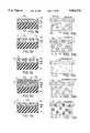
- Pores 28are generally circular in shape as viewed from the top in the plan view of FIG. 2g. Depending on how the track etching is done, pores 28 can be cylindrical or (slightly) conical in three dimensions. For purposes of illustration, pores 28 are represented as cylinders in the drawings.
- the pore diametercan vary from 4 nm to 2 microns. Preferably, the pore diameter lies in the range of 10-200 nm.
- the etchant used for creating pores 28preferably does not significantly attack substrate 20 or conductive region 22.
- components 20, 22, and 24Arespectively consist of ceramic, chromium, and polycarbonate
- the etchingis done in 6.25 normal sodium hydroxide.
- the etch timeis 2-3 minutes for a typical 0.5-micron porous-layer thickness.
- each pore 28 in FIGS. 1g and 2gis considerably narrower than corresponding opening 54.
- corresponding pore 28typically has a diameter of 50 nm.
- Each pore 28is centered on the location of corresponding track segment 50A. Because (a) each track segment 50B was in a straight line with corresponding track segment 50A and (b) each opening 54 is centered on the location of corresponding track segment 50B, each opening 54 is centered on corresponding pore 28.
- a suitable filament metalis now electrochemically deposited to form electron-emissive metal filaments 30 in pores 28 1 overlying lower conductive region 22 as indicated in FIGS. 1h and 2h.
- the depositionis performed in an electrochemical cell, described below, in which conductive region 22 acts as a deposition cathode. After bringing the structure into contact with the cell electrolyte and activating the cell, current flows between cathode 22 and a separate anode. The filament metal uniformly builds up in pores 28 1 starting from conductive region 22. The lower ends of filaments 30 contact region 22.
- the electrochemical depositionis typically performed for a time sufficient to enable the upper ends of pores 30 to be nearly coplanar with top of porous layer 24A. This situation is illustrated in FIG. 1h.
- the depositioncan, however, be performed for a longer time so that filaments 30 bulge slightly out of pores 281 or for a shorter time so that the upper ends of filaments 30 are significantly below the top of layer 24A.
- the upper ends of filaments 30are preferably formed with a noble metal.
- the upper ends of filaments 30consist of platinum when conductive region 22 is chromium.
- Other candidate noble metals for the upper filament endsare gold, and palladium.
- the remaining portions of filaments 30typically consist of the same (noble) metal as the upper ends but can be formed with another metal such as nickel, copper, cobalt, molybdenum, or niobium.
- Elements 30are true filaments for which the ratio of length to maximum diameter is at least 2 and normally at least 3.
- the length-to-maximum-diameter ratiois preferably 10 or more.
- Filaments 30are typically cylinders of circular transverse cross section. Nonetheless, the transverse cross section can be somewhat non-circular. In any case, the ratio of maximum diameter to minimum diameter for each filament 30 is usually no more than 2.
- Filaments 30are all of substantially the same length.
- the filament lengthis 0.1-2.0 microns, typically 1.0 micron.
- filaments 30are likewise situated at random places above conductive region 22. Due to the centering that results from the track formation and etching, filaments 30 are self-aligned to openings 54 1 and therefore to gate electrode 46A.
- FIGS. 1h and 2hcan be directly utilized as a field emitter. Nonetheless, it is advantageous for filaments 30 to extend out of the porous material. It is also desirable for filaments 30 to have sharpened upper ends.
- FIGS. 1i and 2iportions of porous layer 24A exposed through openings 54 1 are removed with an isotropic etchant to form cavities 56 1 around filaments 50 as indicated in FIGS. 1i and 2i. Because gate layer 46A also has openings 54 2 , portions of layer 24A exposed through openings 54 2 are simultaneously removed to form cavities 56 2 . Cavities 56 1 and 56 2 (collectively "56") can extend partway, or all the way, down to lower conductive region 22. FIG. 1i indicates the former case. In either case, filaments 30 now protrude outward beyond the remainder 24F of porous layer 24A. Items 28A 1 and 28A 2 (collectively "28A") in FIGS. 1i and 2i indicate the respective remainders of pores 28 1 and 28 2 .
- Each cavity 56is considerably wider--i.e., has a considerably greater maximum transverse cross-sectional area--than corresponding pore 48A. Also, each cavity 56 is normally somewhat wider than corresponding gate opening 54. Consequently, cavities 56 extend slightly under gate electrode 46A.
- An electropolishing and etching operationis performed on filaments 30 to tailor and Sharpen their upper ends.
- the electropolishingwhich is done first, rounds the upper ends of filaments 30 and reduces their length somewhat.
- the etchsharpens the rounded filament ends.
- the electropolishingis performed in an electrolytic cell in which filaments 30 constitute the anode. After bringing the structure of FIGS. 1i and 2i into contact with the cell electrolyte, a suitable potential is applied between (a) filaments 30 by way of lower conductive region 22 and (b) a separate cathode plate to cause current to flow between filaments 30 and the cathode plate.
- the electropolishingis typically conducted in an operational regime where the rate of metal removal increases with increasing electric field strength. Because the highest electric field, and thus the greatest material removal rate, for each filament 30 occurs at the outer top filament edge, the upper ends of filaments 30 become rounded.
- the electropolishingalso enables filaments 30 to become more uniform in length.
- the filament etchis also typically done by bringing the field-emission structure into contact with the electrolyte of an electrolytic cell in which filaments 30 constitute the anode to which a driving voltage is applied via lower conductive region 22.
- the rate of metal removalvaries with electric field strength and filament morphology in such a way that the rounded upper ends of filaments 30 become pointed.
- the etchcan also be performed according to a chemical technique. If done chemically (rather than electrochemically), undesired etching of gate layer 46A can be avoided by applying an appropriate voltage to layer 46A and/or making suitable materials selection.
- An electropolishing stepis also typically performed to round the edges of patterned gate layer 46A overlying cavities 56.
- Layer 46Aacts as the anode during this step, while filaments 30 serve as the cathode via lower conductive region 22.
- FIGS. 1j and 2jshow the final structure in which item 46B is the edge-rounded remainder of gate layer 46A. Items 30B are the sharpened remainders of filaments 30. Each cavity 56 1 , in combination with underlying pore 28A, forms a dielectric open space for corresponding sharpened filament 30B.
- Openings 54can alternatively be created by etching through holes whose diameter is considerably smaller than openings 54 rather than using apertures 52 whose diameter is approximately the same as openings 54. More specifically, after forming charged-particle tracks 50 in the structure of FIG. 1c, track segments 50B are etched to create relatively narrow pores through insulating layer 48. The portions of metal layer 46 exposed through these narrow pores are removed with an isotropic etchant that attacks metal layer 46 much more than insulating layers 24 and 48 to form openings 54 down to layer 24. Because the etch is isotropic, openings 54 now extend slightly under insulating layer 48. From this point on, the structure is further processed in the manner described above for FIGS. 1f-1j.
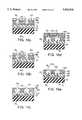
- FIGS. 3a-3eillustrate a sequence of steps for converting filaments 30 in the structure of FIG. 1i into pointed electron-emissive filaments that extend beyond the top of the gate electrode. For convenience, FIG. 1i is repeated here as FIG. 3a.
- a thin masking layer 86 of a lift-off materialis formed on the partially finished field-emission structure of FIG. 3a in such a way that the lift-off material fully covers gate layer 46A but does not cover the tops of filaments 30. See FIG. 3b.
- the lift-off materialis present in the portions of cavities 56 1 situated to the sides of filaments 30.
- the thickness of layer 86is typically a fraction of (i.e., less than) the average diameter of gate openings 54.
- Lift-off layer 86is typically created according to a physical deposition technique, such as evaporation, in which atoms of the lift-off material impinge, and thereby accumulate, on the top of gate layer 46A in a direction that is at a small angle to the (unshown) lower surface of substrate 20 and thus at a small angle to the top of gate layer 46A.
- a physical deposition techniquesuch as evaporation, in which atoms of the lift-off material impinge, and thereby accumulate, on the top of gate layer 46A in a direction that is at a small angle to the (unshown) lower surface of substrate 20 and thus at a small angle to the top of gate layer 46A.
- evaporationatoms of the lift-off material impinge, and thereby accumulate, on the top of gate layer 46A in a direction that is at a small angle to the (unshown) lower surface of substrate 20 and thus at a small angle to the top of gate layer 46A.
- the impingement angleis set
- blunted metallic tips 88A 1are respectively formed on the upper surfaces of filaments 30 as depicted in FIG. 3c.
- Metal tips 88A 1are preferably created according to a physical deposition technique, such as evaporation, in which atoms of the tip metal are directed toward the top of the field-emission structure in a direction largely perpendicular to the lower surface of substrate 20 and thus in a direction largely perpendicular to the top of gate layer 46A.
- atoms of the tip metalpass through gate openings 54 1 to form tips 88A 1 .
- annular portions 88B 1 of the tip metalrespectively accumulate around filaments 30 at the bottoms of cavities 56 1 .
- Atoms of the tip metalalso pass through gate openings 54 2 (not shown) to form pieces (not shown) of the tip metal along parts of insulating layer 24F exposed through cavities 56 2 (also not shown). These pieces of the tip metal do not contact lower conductive region 22. Accordingly, they do not affect the electrical operation of the final field emitter.
- a layer 88C of the tip metalaccumulates on lift-off layer 86 during the tip deposition. As the thickness of layer 88C increases, layer 88C typically grows slightly in the lateral direction. Although this lateral growth gradually reduces the size of the openings through which the tip metal can deposit on filaments 30 and does affect the shape of metal portions 88B 1 , the deposition of the tip metal is terminated before the tip-deposition openings through layer 88C become so small that the tip metal starts to accumulate non-uniformly (e.g., to start forming conically-ended tips) on the upper surfaces of filaments 30.
- FIG. 4apresents an enlarged view of one of lengthened filaments 30/88A 1 at the stage depicted in FIG. 3c.
- the presence of metal portion 88B 1 along the length of filament 30/88A 1is normally not electrically significant.
- a noble metalis preferably employed for the tip metal.
- the tip metalconsists of platinum when components 22, 46A, and 30 are respectively formed with chromium, molybdenum, and platinum.
- each filament 30 and overlying tip 88A 1consist of the same metal.
- the tip metalcan be a non-noble metal, such as molybdenum or niobium, capable of being physically deposited in the way described above. The amount of tip metal deposited depends on the desired length (or height) of the final electron-emissive elements.
- Lift-off layer 86is now removed by subjecting the structure to a chemical etchant that attacks the lift-off material but does not significantly attack any other materials in the structure. During the removal of layer 86, layer 88C is lifted off to produce the structure shown in FIG. 3d.
- FIG. 3eillustrates the exemplary case in which substantially all the tailoring and sharpening is done on upper ends 88A 1 which thereby become pointed tips 88D 1 .
- FIG. 4bpresents an enlarged view of typical filament 30/88D 1 at the stage shown in FIG. 3e.
- a further electropolishing stepis normally also performed in the manner described above to round the edges of gate layer 46A overlying cavities 56 1 .
- Patterned gate electrode 46B in FIG. 3eis the rounded-edge remainder of gate layer 46A.
- FIGS. 5a-5edepict another sequence of steps for converting filaments 30 in the gated field-emission structure of FIG. 1i into longer pointed filaments.
- FIG. 1iis likewise repeated here as FIG. 5a.
- Lift-off layer 86is formed on gate layer 46A in the manner described above. See FIG. 5b which is a repeat of FIG. 3b. At this point, the process of FIG. 5 diverges from that of FIG. 3.
- Pointed metallic tips 90A 1are formed directly on the upper surfaces of filaments 30 as indicated in FIG. 5c. Tips 90A 1 , basically consist of cylinders with conically shaped upper ends.
- Metal tips 90A 1are typically created according to a double-source physical deposition technique in which (1) atoms of a tip metal deposit on top of the structure in a direction largely perpendicular to the (unshown) lower surface of substrate 20 and thus in a direction largely perpendicular to the upper surface of gate layer 46A and (2) atoms of a closure material simultaneously impinge, and thereby accumulate, on the upper surface of layer 46A in a direction that is at a small angle to the lower surface of the substrate 20 while either the partially finished field emitter or the sources of the tip and closure materials are rotated at constant speed about an axis perpendicular to the lower surface of substrate 20 in order to obtain a spatially uniform deposition. Both parts of the deposition are usually done by evaporation.
- the impingement angle for the closure materialis small enough that substantially none of the closure material passes through gate openings 54 to accumulate on filaments 30 or on the portions of insulating layer 24F exposed through cavities 56. Only the tip metal passes through openings 54. Accordingly, the tip metal accumulates on filaments 30 to form pointed tips 90A 1 . Annular portions 90B 1 of the tip metal also respectively accumulate around filaments 30 at the bottoms of cavities 56 1 . As in the process of FIG. 3, electrically inconsequential pieces (not shown) of the tip metal are formed along the parts of insulating layer 24F exposed through cavities 56 2 .
- a composite layer 92 of the tip and closure materialsaccumulates on lift-off layer 86 during the tip deposition. Because the impingement angle for the closure material is less than 90°, composite layer 92 expands laterally as its thickness increases so as to progressively close the openings through which the tip metal can accumulate to form tips 90A 1 and metal portions 90B 1 .
- the depositionis conducted for a time sufficiently long that the tip-deposition openings through layer 92 close fully, and layer 92 becomes a continuous film. Consequently, filament tips 90A 1 are created generally in the shape of cones. Each filament 30 in combination with overlying tip 90A 1 constitutes a lengthened, pointed electron-emissive filament.
- the tip metalis normally the same as in the process of FIG. 3.
- the height of tips 90A 1depends on the rate at which the tip and closure materials are deposited and on the impingement angle for the closure material.
- FIG. 6presents an enlarged view of one of filaments 30/90A 1 at the stage shown in FIG. 5c.
- Lift-off layer 86 and composite layer 92are subsequently removed according to a conventional etching technique. See FIG. 5d.
- An electropolishing stepis preferably done to round the edges of gate layer 46A overlying cavities 56 1 .
- the electropolishingis preferably conducted in the way described above.
- FIG. 5eshows the final structure in which item 46B is again the rounded-edge remainder of gate layer 46A. Because the upper ends of metal tips 90A 1 are generally in the shape of cones, there is no need to perform an electropolishing and etching operation on tips 90A 1 .
- the process in FIG. 5can be modified in a number of ways.
- the deposition of the closure materialcan be deleted; advantage can be taken of the fact that layer 92, now solely consisting of the tip metal, expands slightly in the lateral direction as its thickness increases. In this case, tips 90A 1 grow higher.
- the deposition of the tip and closure materialscan be terminated before the tip-deposition openings through layer 92 fully close. Since tips 90A 1 are thereby produced with unsharpened upper ends, an abbreviated electropolishing and etching operation can be performed to sharpen tips 90A 1 .
- FIGS. 7a-7hillustrate a sequence of fabrication steps by which the process of FIG. 1 is modified starting at the stage shown in FIG. 1f, repeated here as FIG. 7a, to create a gated field emitter having conically pointed filamentary electron-emissive elements whose tips are respectively wider at their bases than the underlying filamentary segments.
- Portions of insulating layer 24 exposed through gate openings 54 1are removed with an isotropic chemical etchant to form cavities 94 1 that extend partway, but not all the way, through layer 24 as shown in FIG. 7b. Portions of layer 24 exposed through gate openings 54 2 (not shown) are simultaneously removed to form cavities 94 2 (likewise not shown) that extend partway through layer 24.
- Each of cavities 94 1 and 94 2extends slightly under gate layer 46A.
- the etchantpreferably attacks the damaged material along track segments 50A at approximately the same rate as the undamaged insulating material of layer 24. Consequently, the portion of each track segment 50A, of which only segments 50A 1 are shown in FIG. 7b, at the bottom of corresponding cavity 94 is not significantly attacked during the etch. The remainder of insulating layer 24 is indicated as item 24G in FIG. 7b.
- Pores 96 1are thereby created through layer 24G along the remaining portions of track segments 50A 1 at the bottom of cavities 94 1 as shown in FIG. 7c.
- Pores 96 2(not shown) are simultaneously etched through layer 24G along the remaining (unshown) portions of track segments 50A 2 at the bottom of cavities 94 2 (also not shown). Item 24H in FIG. 7c is the remainder of insulating layer 24G.
- each pore 96is thereby centered on the location of corresponding track segment 50A. Pores 96 typically have the same physical/spatial characteristics as given above for pores 28. In addition to being narrower than overlying cavity 94, each pore 96 is considerably narrower than corresponding gate opening 54. Because (a) each track segment 50B was in a straight line with corresponding track segment 50A and (b) each gate opening 54 is centered on the location of corresponding track segment 50B, each opening 54 is centered on corresponding pore 96.
- An appropriate filament metalis electrochemically deposited to create metal filaments 98 that substantially fill pores 96 1 over lower conductive region 22 as shown in FIG. 7d.
- the filament depositionis performed in the manner used to Create filaments 30 in the process of FIGS. 1 and 2. Since there is no electrical contact at the bottoms of pores 96 2 located directly above substrate 20, substantially none of the filament material accumulates in pores 96 2 . Consequently, the electrochemical nature of the process enables the deposition to be selective even through there is a gate opening for each pore 96.
- Filaments 98can be formed with a noble metal such as platinum, gold, or palladium.
- the filament metalcan also be a non-noble metal such as nickel, copper, cobalt, molybdenum, or niobium.
- Metal filaments 98have the same basic length, diameter, length-to-diameter, and cross-sectional characteristics as filaments 30.
- the length-to-maximum-diameter ratio for filaments 98is preferably 10 or more.
- filaments 98can be made longer than filaments 30 by increasing the thickness of insulating layer 24 and appropriately controlling the depth of the cavity etch.
- the centering that results from the track formation and etchingenables filaments 98 to be self-aligned to gate openings 54 1 and thus to gate layer 46A.
- a thin masking layer 100 of a lift-off materialis formed on the field-emission structure in such a manner that the lift-off material fully covers gate layer 46A but does not cover the tops of filaments 98. See FIG. 7e.
- Lift-off layer 100is preferably created according to the technique used to create lift-off layer 86 in the process of FIG. 3 or 5.
- a tip metalis introduced through gate openings 54 1 into cavities 94 1 to form pointed, generally conical metallic tips 102 1 that respectively contact filaments 98 as indicated in FIG. 7f.
- the tip metalis normally the same as in the process of FIG. 5.
- each metallic tip 102 1is normally greater than the diameter of underlying filament 98. Consequently, tips 102 1 extend laterally over adjoining portions of insulating layer 24H.
- Each filament 98 and overlying tip 102 1form a composite electron-emissive element whose maximum diameter occurs at a point between--i.e., spaced apart from--the ends of that element.
- Metal tips 102 1are preferably formed according to a double-source physical deposition technique using the tip metal and a closure material in the same way that tips 90A 1 are created in the process of FIG. 5.
- the impingement angle for the closure materialwhich helps close the openings through which the tip metal enters cavities 94, is sufficiently small that substantially none of the closure material passes through gate openings 54 1 , to accumulate on filaments 98 or on portions of insulating layer 24H exposed through cavities 94 1 .
- the tip metalalso passes through gate openings 54 2 (not shown) to form pieces (not shown) of the tip metal along parts of layer 24H exposed through cavities 94 2 (also not shown). These pieces of the tip metal are electrically inconsequential since they do not contact lower conductive region 22.
- a composite layer 104 of the tip and closure materialsaccumulates on lift-off layer 100 in the same way that composite layer 92 is created in the process of FIG. 5.
- the tip-deposition openings through which the tip metal passes to form tips 102 1progressively close in a substantially uniform manner. Tips 102 1 are thus formed in the shape of cones respectively centered on filaments 98. Accordingly, tips 102 1 are self-aligned to gate openings 54 1 .
- Each filament 98 and overlying metal cone 102 1form a composite electron-emissive element.
- FIG. 7gillustrates the resulting structure.
- the final step in the fabrication processis to round the edges of gate layer 46A overlying cavities 94 1 as shown in FIG. 7h.
- the edge roundingis preferably done by an electropolishing step in the way described above.
- item 46B in FIG. 7his the rounded-edge remainder of gate layer 46A.
- Each cavity 94 1 and underlying pore 96 1form a dielectric open space for corresponding electron-emissive element 98/102 1 . Since pores 96 1 are distributed randomly across insulating layer 24H, electron-emissive elements 98/102 1 are situated at random locations above lower conductive region 22.
- FIGS. 8a-8hillustrate how a gated field emitter can be fabricated according to a variation of the composite process of FIGS. 1a-1f and FIG. 7 to facilitate creation of cavities that extend partway through insulating layer 24 along its upper surface below the gate openings.
- insulating layer 24is deposited on conductive region 22 as a lower sublayer 24I and an upper sublayer 24J which is selectively etchable with respect to sublayer 24I.
- Gate layer 46 and further insulating layer 48are then sequentially deposited to produce the initial structure shown in FIG. 8a.
- FIG. 8billustrates the formation of tracks 50 through insulating layer 48 and sublayers 24I and 24J of insulating layer 24.
- Track segments 50A 1extend through both sublayers 24I and 24J down to lower conductive region 22.
- Track segments 50A 2(not shown) extend through sublayers 24I and 24J directly down to substrate 20.
- the incidental structural facets created as a result of track segments 50A 2are not electrically consequential and, for simplicity, are not mentioned further in the discussion of FIG. 8.
- FIGS. 8c and 8dillustrate the formation of apertures 52 1 through insulating layer 48, the formation of gate openings 54 1 through gate layer 46, and the removal of the remainder 48A of layer 48.
- Portions of insulating sublayer 24J exposed through gate openings 54 1are removed with an isotropic chemical etchant that attacks sublayer 24J much more than sublayer 24I to form cavities 106 1 in composite insulating layer 24.
- the etchis preferably done in a single step.
- the portions of track segments 50A 1 extending through sublayer 24Jcan be etched to form pores through layers 24J after which the pores are widened to create cavities 106 1 .
- Insulating sublayer 24Iacts as an etch stop to prevent cavities 106 1 from going deeper into layer 24.
- FIG. 8eillustrates the resulting structure in which item 24K is the remainder of layer 24J.
- FIGS. 8f-8hillustrate the etching of pores 108 1 through insulating sublayer 24I, the formation of metallic filaments 110 in pores 108 1 , and the formation of pointed, generally conical metal tips 112 1 that contact filaments 110 in a self-aligned manner within cavities 106 1 .
- Item 24L in FIGS. 8f-8his the remainder of sub layer 24I.
- An electropolishing stepis typically employed to round the edges of the remainder 46A of gate layer 46.
- each cone 112 1 in FIG. 8his usually greater than the diameter of underlying filament 110. Cones 112 1 therefore extend laterally over adjoining material of insulating sublayer 24L. Each filament 110 and overlying cone 112 1 form a composite electron-emissive element whose maximum diameter occurs at a point between the ends of that element.
- the metal portions that connect lower conductive region 22 to conical tips 88D 1 , 90A 1 , 102 1 , and 112 1 in the structures produced according to the processes of FIGS. 3, 5, 7, and 8have been described as filaments.
- these metal portionscould simply be metallic pedestals that do not necessarily have the elongated characteristics of filaments, such as the filamentary characteristics described above for filaments 30 in the process of FIGS. 1 and 2.
- the length (or height) of a pedestalcould be less than its diameter.
- FIG. 1can be modified to create a gated field-emission structure in which the electron-emissive elements consist solely of cones. That is, no filaments or pedestals lie between lower conductive region 22 and the cones.
- FIGS. 9a-9e(collectively “FIG. 9") and FIGS. 10a-10e (collectively “FIG. 10") illustrate a sequence of steps for creating such a cone-based gated field emitter starting from the structure depicted in FIGS. 1f and 2f. These two figures are respectively repeated as FIGS. 9a and 10a.
- dielectric open spaces 114 1are etched through insulating layer 24 down to lower conductive region 22 at the locations of gate openings 54 1 . See FIGS. 9b and 10b.
- Dielectric open spaces 114 2are similarly formed through layer 24 at the locations of gate openings 54 2 .
- Each of dielectric open spaces 114 1 and 114 2extends slightly under gate layer 46A. The etch is preferably done in one step, but can be performed in two steps as described above for cavities 106 1 in the process of FIG. 8. Item 24M in FIG. 9b is the remainder of layer 24.
- a thin masking layer 116 of a lift-off materialis created on the structure so as to fully cover gate layer 46A as shown in FIGS. 9c and 10c.
- Lift-off layer 116extends slightly over the edges of gate layer 46A along openings 54.
- Layer 116is preferably created according to the technique employed to form lift-off layer 86 in the process of FIG. 5.
- a cone metalis introduced through gate openings 54 1 into cavities 114 1 to form generally conical electron-emissive elements 118 1 on lower conductive region 22. See FIGS. 9d and 10d. Electron-emissive cones 118 1 are preferably formed according to the double-source physical deposition technique used to create filament tips 90A 1 in the process of FIG. 5. The tip metal in the process of FIG. 5 is now the cone metal. Some of the cone metal also passes through gate openings 54 2 to form metal portions 118 2 in cavities 114 2 . Metal portions 118 2 do not contact lower conductive region 22 and therefore do not affect the electrical operation of the final field emitter.
- a composite layer 120 of the cone and closure materialsaccumulates on lift-off layer 116 in the same manner that composite layer 92 is formed in the process of FIG. 5.
- the cone-deposition openings through which the cone metal enters cavities 114close in a substantially uniform manner.
- tips 118 1are formed in the shape of cones self-aligned to gate openings 54 1 .
- FIG. 9edepicts the resulting structure. Because openings 54 1 are situated at random locations across gate layer 46A, cones 118 1 are located in random places above lower conductive region 22. An electropolishing step may be performed in the manner described above to round the edges of the remainder 46A of gate layer 46.
- the lift-off layercan be provided at an earlier stage in the process.
- the lift-off layercan be deposited on gate layer 46 at the beginning of the process before the deposition of further layer 48 in FIG. 1b.
- the lift-off layerundergoes the same operations that layer 48 undergoes except that the lift-off layer is not removed when the etched remainder 48A of layer 48 is removed. In fact, the lift-off layer could even consist of layer 48A.
- FIGS. 11 and 12illustrate the starting point for manufacturing implementations of the present field emitter in which lower conductive region 22 consists of a highly conductive layer 22A situated under a highly resistive (but still conductive) layer 22B. As shown in FIG. 12, each of the lines that form region 22 consists of segments of both of layers 22A and 22B.
- Highly conductive layer 22Aconsists of one or more of the materials described above for layer 22.
- Resistive layer 22Bis typically formed with cermet (ceramic with embedded metal particles), doped polycrystalline silicon, or doped silicon carbide.
- FIGS. 13.1-13.4respectively depict how the final structures of FIGS. 1j, 3e, 7h, and 9e appear when lower conductive region 22 consists of highly conductive layer 22A and highly resistive layer 22B.
- the lower ends of electron-emissive elements 30B, 30/88D 1 , 98/102 1 , or 118 1contact resistive layer 22B.
- the resistance between each electron-emissive element and layer 22Ais at least 10 6 ohms, typically 10 8 ohms or more.
- FIGS. 14a-14lillustrate how a gated field emitter having a focusing control electrode is so manufactured. This field emitter is also suitable for flat-panel television applications.
- the field emitteris built on insulating substrate 20 over which lower conductive region 22 is provided as shown in FIG. 14a.
- Insulating layer 24, metal layer 46, and second insulating layer 48are formed in sequence on the top of the structure. See FIG. 14b.
- Components 20, 22, 24, 46, and 48all have the characteristics described above.
- a second electrically conductive layer 60is formed on top of second insulating layer 48.
- Conductive layer 60later becomes the focusing electrode.
- a further electrically insulating layer 62is formed on top of layer 60.
- Layers 62 and 60respectively have largely the same characteristics as insulating layer 48 and metal layer 46. Accordingly, layer 62 consists of insulating material, and layer 60 consists of metal.
- the structureis subjected to energetic charged particles traveling in a direction largely perpendicular to the (unshown) lower substrate surface and thus in a direction generally perpendicular to the upper structural surface.
- the charged particlespass through layers 62, 60, 48, 46, and 24 and into the underlying material to form straight tracks through insulating layers 62, 48, and 24. See FIG. 14c .
- Each trackis divided into (a) a "64A” segment extending through insulating layer 24, (b) a “64B” segment extending through insulating layer 48, and (c) a "64C” segment extending through insulating layer 62.
- the charged particlesdo not cause any significant damage to metal layers 60 and 46 and therefore do not create any tracks through layers 60 and 46.
- the tracksfall into two categories: (a) segments 64A 1 , 64B 1 , and 64C 1 (collectively “64 1 ”) extending respectively through portions of layers 24, 48, and 62 overlying lower conductive region 22, and (b) segments 64A 2 , 64B 2 , and 64C 2 (collectively "64 2 ") extending respectively through portions of layers 24, 48, and 62 not overlying region 22.
- Track segments 642although not shown in the drawings, are analogous to track segments 50 2 --i.e., segments 50A 2 and 50B 2 --depicted in FIGS. 2c and 2e for the process of FIGS. 1 and 2.
- Charged-particle tracks 64 1 and 64 2extend parallel to one another in a direction generally perpendicular to the upper structural surface. Tracks 64 have the same basic characteristics, and are formed in the same way, as tracks 50 described above.
- Generally circular poresare formed through insulating layer 62 along track segments 64C down to metal layer 60 by bringing layer 62 into contact with a chemical etchant that attacks the damaged 64C track material much more than the undamaged material of layer 62.
- the poresare then broadened by continuing the etch into the undamaged material to form apertures 66 1 and 66 2 respectively along the pores created by etching tracks 64B 1 and 64B 2 . See FIG. 14d.
- Apertures 66 2although not shown in the drawings, are analogous to apertures 52 2 depicted in FIG. 2d.
- apertures 66 1 and 66 2are formed uniformly in largely the same manner as that described above for creating apertures 52, with one notable difference.
- the etch time for apertures 66is somewhat longer than the etch time for apertures 52. Consequently, apertures 66 have substantially the same characteristics as apertures 52 but are larger in diameter. In particular, apertures 66 reach an average diameter of 20-400 nm, typically 190 nm, along the bottom of the remainder 62A of insulating layer 62.
- openings 68 1are thereby created down to insulating layer 48 through the portions of layer 60 overlying lower conductive region 22 as shown in FIG. 14e. Openings 682 are simultaneously created down to layer 48 through portions of layer 60 not overlying region 22.
- openings 68 2are analogous to openings 54 2 depicted in FIG. 2e.
- the remainder 60A of metal layer 60 in FIG. 14eis the patterned focusing electrode for the field emitter.
- openings 68 1 and 68 2are typically performed in the same way as the metal etch employed to create openings 54 in the process of FIGS. 1 and 2. As a result, each opening 68 is centered on the location of corresponding track segment 64C.
- poresare created in the damaged insulating material along segments 64B by bringing the structure into contact with a chemical etchant that attacks the damaged 64B track material much more than the undamaged material of layer 48. The etch is continued into the undamaged insulating material of layer 48 to broaden the pores. Apertures 70 1 and 70 2 are thereby created respectively along track segments 64B 1 and 64B 2 . See FIG. 14f. Although not shown in the drawings, apertures 70 2 are analogous to apertures 52 2 shown in FIG. 2d.
- the thickness and lateral extent of insulating layer 62Amay be reduced during the etch depending on whether insulating layer 48 is selectively etched with respect to layer 62A or not.
- FIG. 14fillustrates the case in which layer 62A is not significantly affected.
- etching apertures 70 1 and 70 2(collectively "70") is performed in the laterally uniform manner described above for etching apertures 52 in the process of FIGS. 1 and 2. Small pieces of insulating material lying below focusing layer 60A along openings 68 are normally removed during the etch so as to undercut layer 60A slightly. Item 48B in FIG. 14f is the remainder of insulating layer 48. Aside from the undercutting of layer 60A, apertures 70 have substantially the same characteristics as apertures 52, including the same average aperture diameter along gate layer 46.
- the portions of metal layer 46 exposed through apertures 70 1are removed with an anisotropic etchant to create generally circular openings 54 1 down to portions of insulating layer 24 that overlie lower conductive region 22 as shown in FIG. 14g.
- the portions of layer 46 exposed via apertures 70 2are simultaneously removed to create generally circular openings 54 2 (not shown) down to the portions of layer 24 situated directly above substrate 20.
- the remaining portion 46A of gate layer 46 in FIG. 14gis again the gate electrode for the field emitter.
- each opening 54is centered on the location of corresponding track segment 64B.
- insulating layer 62Ais removed at some point after openings 54 are created. This can, for example, be done directly after formation of openings 54 as shown in FIG. 14h. If the etchant does not significantly attack electrode 60A, layer 62A can be removed between the step in which openings 68 are created (to define electrode 60A) and the step in which openings 54 are created.
- FIG. 14his substantially the same as the structure of FIG. 1f.
- Track segments 64A 1 in FIG. 14hare the same as track segments 50A 1 in FIG. 1f.
- the structure of FIG. 14his further processed in the same way as the structure of FIG. 1f.
- FIGS. 14i-14lrespectively correspond to FIGS. 1g-1j. The processing description presented above in connection with FIGS. 1g-1j applies directly to FIGS. 14i-14l with each track segment "50A" now being referred to as "64A".
- the exposed portions of insulating layer 48B below the edges of focusing electrode 60Aare partially etched back.
- the etchbackis either performed during the etch to create cavities 56 in porous insulating layer 24A or as a separate step.
- the edges of layer 60Aextend laterally beyond the remainder 48C of insulating layer 48B.
- Item 24Fis again the remainder of porous layer 24A.
- edges of focusing layer 60Aare typically rounded during the same electropolishing step used to round the edges of gate layer 46A.
- Item 60B in FIG. 14lis the rounded-edge patterned remainder of focusing layer 60A.
- Item 46Bis again the rounded-edge patterned remainder of gate layer 46A.
- items 30Bare again the sharpened filaments.
- Lower conductive region 22 in FIG. 14lmay again consist of highly resistive layer 22A and overlying highly conductive layer 22B as described above. Also, the steps employed to create focusing electrode 60B above insulating layer 48C can be repeated to create one or more further control electrodes above layer 60B. In doing so, the centering that results from the track formation and etching enables each further control electrode to be self-aligned to filaments 30B.
- the process of FIG. 14can be modified to produce a gated field emitter which has one or more control electrodes above the gate electrode and which also has electron-emissive elements of the type shown in FIG. 3e, 5e, 7h, 8h, or 9e.
- This modificationis achieved in a manner similar to that used for modifying the process of FIG. 1 according to the steps shown in FIG. 3, 5, 7, 8, or 9.
- FIGS. 15a-15d(collectively “FIG. 15") generally illustrate how the sequence of steps in FIG. 9 is applied to the process of FIG. 14 to create a gated field emitter having both a focusing electrode and conical electron-emissive elements.
- the starting point for the modificationis FIG. 14g repeated here as FIG. 15a.
- dielectric open spaces 114 1are etched through layer 24 down to lower conductive region 22 in the manner described above.
- FIG. 15bshows the resulting structure.
- Dielectric open spaces 114 2are similarly formed through layer 24.
- the exposed portions of insulating layer 48B below the edges of focusing electrode 60Aare also etched back. Depending on the properties of layers 48B and 24, this etchback is either performed during the etch step to form dielectric open spaces 114 or as a separate step. If layers 48B and 24 are etched at the same time, the damaged insulating material along track segments 64A 1 is normally attacked at a considerably faster rate than the undamaged material of insulating layer 24. This helps to reduce the etching of layer 48B and thereby avoid excessive further undercutting of focusing layer 60A. In any case, item 24M in FIG. 15b is again the remainder of layer 24. Item 48D is the remainder of layer 48B.
- Conical electron-emissive elements 118 1are then formed in dielectric open spaces 114 1 as indicated in FIG. 15c.
- Various techniques that take focusing electrode 60A into accountcan be used.
- a lift-off layercan be created on focusing electrode 60A in the same way that lift-off layer 116 is created in the process of FIG. 9 except that the impingement angle is increased so that pieces of the lift-off material accumulate on portions of gate layer 46A exposed through gate openings 54 1 .
- the remainder of the procedure for creating metal cones 118 1is then performed as described above for the process of FIG. 9.
- the pieces of the lift-off material on gate layer 46Aare removed along with overlying composite pieces of the cone and closure materials.
- FIG. 15dshows the final structure. Items 46B and 60B are again the rounded-edge remainders of layers 46A and 60A. Due to the uniform nature of the deposition/lift-off technique employed to create cones 118 1 , layers 46B and 60B are both self-aligned to cone 118 1 .
- FIGS. 16a-16e(collectively “FIG. 16") generally illustrate how the process of FIG. 14 is modified to produce a gated field emitter that has a focusing electrode and electron-emissive elements consisting of cones situated on pedestals.
- the starting pointis the structure of FIG. 14f repeated here as FIG. 16a.
- the incidental structural facets created as a result of track segments 64A 2(not shown here) are electrically inconsequential and, for simplicity, are not mentioned further.
- portions of gate layer 46 exposed through apertures 70 1are removed with an isotropic etchant.
- the etchingis continued uniformly into portions of layer 46 underlying layer 48B to create generally circular gate openings 120 1 down to portions of insulating layer 24 that overlie lower conductive region 22. See FIG. 16b.
- the etchantdoes not significantly attack focusing layer 60A or any of the other components of the structure except for layer 46.
- Each gate opening 120 1has a greater diameter than overlying opening 68 1 in layer 60A. Also, each gate opening 120 1 is centered on the location of corresponding track segment 64B 1 (shown earlier in FIG. 14e). The remainder 46C of layer 46 in FIG. 16b is the patterned gate electrode for the field emitter.
- Insulating layer 62Ais removed as indicated in FIG. 16c.
- layer 62Acould be removed earlier in the process--e.g., as early as directly after the creation of openings 68 1 to define focusing layer 60A.
- Portions of insulating layer 24 exposed through gate openings 120 1are subsequently removed with an isotropic etchant to form cavities 122 1 that, like cavities 94 1 in FIG. 7b, extend partway through layer 24.
- Each cavity 122 1extends slightly under gate electrode 46C.
- insulating layer 48B below the edges of focusing electrode 60Aare also etched back. Depending on the properties of insulating layers 24 and 8B, this etch back can be done during the formation of cavities 122 1 or as a separate step. Item 48E in FIG. 16c is the remainder of layer 48B.
- Pores 96 1are created through insulating layer 24 along the remaining portions of track segments 64A 1 at the bottom of cavities 122 1 in the same way that pores 96 1 are created in the process of FIG. 7. Each gate opening 120 1 is thereby centered on corresponding pore 96 1 . Item 24N in FIG. 16c is the remainder of layer 24.
- Metal filaments 98are formed in pores 96 1 in the same manner as in the process of FIG. 7. Due to the centering that results from the track formation and etching, filaments 98 are self aligned to gate openings 120 1 and therefore to gate electrode 46C.
- a lift-off layer 124is formed on focusing electrode 60A. See FIG. 16d. None of the lift-off material accumulates on the tops of filaments 98. Likewise, none of the lift-off material normally accumulates on gate electrode 46C.
- Conical tips 102 1are formed on filaments 98 according to a double-source physical deposition as in the process of FIG. 7.
- a composite layer 126 of the tip and closure materialsforms on lift-off layer 124 as shown in FIG. 16d. Because each gate opening 120 1 has a greater diameter than overlying opening 68 1 in focusing electrode 60A, substantially none of the tip or closure material accumulates on gate electrode 46C during the deposition.
- Each filament 98 and overlying cone 102 1again form a composite longitudinally symmetric electron-emissive element.
- Each cavity 122 1 and underlying pore 96 1constitute a dielectric open space for composite element 98/102 1 .
- Lift-off layer 124 and composite layer 126are removed according to conventional technique to produce the structure shown in FIG. 16e.
- the fabrication of the field emitteris normally completed by performing an electropolishing step to round the edges of electrodes 46C and 60A.
- the size of gate openings 120 1 in the process of FIG. 16is not determined by the size of apertures 70 1 . Accordingly, the size of aperture 70 1 can be decreased in the process of FIG. 16 to reduce the undercutting of focusing electrode 60A.
- each electron-emissive elementcontain a highly resistive, but still conductive, portion for improving emission uniformity and limiting emitter currents to prevent short-circuit and arcing failures.
- the highly resistive portionpreferably contacts lower conductive metal region 22.
- the resistance for the highly resistive portionis normally at least 10 6 ohms, preferably 10 8 ohms or more. More specifically, the resistance for the highly resistive portion is at least 10 10 ohms.
- the highly resistive portionstypically consist of cermet, doped polycrystalline silicon, or doped silicon carbide.
- FIG. 17.1illustrates how each electron-emissive filament 30B in FIG. 1i or 14l consists of a lower highly resistive portion 30C and an upper highly conductive electron-emissive pointed tip 30D.
- FIG. 17.2illustrates how each electron-emissive cone 118 1 in FIG. 9e or 15d consists of a lower highly resistive portion 118A 1 and an upper highly conductive electron-emissive portion 118B 1 .
- an initial part of the emitter depositionis performed with a highly resistive material rather than the metal(s) specified above.
- filaments 30 in FIG. 3 or 5either all or a lower part of each filament 30 is formed with highly-resistive material. The same applies to filaments 98 in FIG. 7h or 16e and to filaments 110 in FIG. 8h.
- the electron-emissive cones in the field emitters of the inventionhave, for simplicity, been illustrated in the drawings as being of right circular shape (i.e., a right triangle rotated about one of its legs).
- the conesinvariably have surfaces that differ somewhat from a right circular shape.
- the surfaces of the conestypically bend inward slightly as shown in FIG. 18.1 for cones 102 1 of FIG. 7h or 16e and as depicted in FIG. 18.2 for cones 118 1 of FIG. 9e or 15d.
- FIGS. 19.1-19.4illustrate several longitudinal shapes that filaments 30B can have in the final field emitters of FIG. 1j and 14l.
- filaments 30Bcan be solid cylinders except at their upper ends. If tracks 50 are etched in such a manner as to create pores 28 as inverted cones, filaments 30B can be inverted solid cones which taper down in transverse cross section from just below their upper ends to their lower ends in the manner shown in FIGS. 19.3 and 19.4.
- the electron-emissive tips at the upper ends of filaments 30Bcan be generally rounded as indicated in FIGS. 19.1 and 19.3 or sharply pointed as indicated in FIGS. 19.2 and 19.4.
- FIG. 20depicts the electrochemical deposition system employed during the electrochemical filament deposition operations described above.
- the electrochemical systemconsists of an electrochemical cell 72 and a power supply and control system 74.
- electrochemical cell 72consists of cell electrolyte 76, a surrounding sidewall 78, an O-ring 80, an anode 82, and a cathode 84 formed by part of the structure on which metal is being deposited.
- Cathode 84includes lower conductive region 22 to which power supply and control system 74 is connected.
- FIG. 20specifically illustrates the filament deposition in the process of FIGS. 1 and 2.
- the electrochemical system shown in FIG. 20operates according to a constant-current technique.
- a constant-voltage electrochemical deposition systemcould be used.
- the field emitters of the present inventionoperate in the following way.
- An anode (or collector) structureis situated a short distance away from the top of each field emitter.
- a voltageis applied between the anode and a selected one of the lines that forms lower conductive region 22.
- the particular electron-emissive elements above the selected linethen emit electrons collected at the anode structure.
- the gate electrodeextracts electrons from the filaments and controls the magnitude of the electron beam.
- the focusing electrodewhen present, focuses the electron beam.
- the various electron-emissive elements and charged-particle tracks (or track segments)have longitudinal axes (not shown). Each electron-emissive element is generally symmetric about its longitudinal axis.
- a reference to an etch as being performed along a charged-particle track through an insulating layermeans that the removed material occupied a volume containing at least part of the track's longitudinal axis in the insulating layer.
- substrate 20could be deleted if lower conductive region 22 is a continuous layer of sufficient thickness to support the structure.
- Insulating substrate 20could be replaced with a composite substrate in which a thin insulating layer overlies a relatively thick non-insulating layer that furnishes the necessary structural support.
- Substrate 20 and/or conductive region 22could be formed under insulating layer 24 after charged-particle tracks 50 are formed through it.
- Gate layer 46could be patterned into lines running perpendicular to the lines that form region 22.
- electrochemical depositionscould be performed by a full immersion technique with the sides of the field emitter suitably protected to avoid unwanted deposition.
- Thermal annealingcould be used to modify the filament shape.
Landscapes
- Engineering & Computer Science (AREA)
- Chemical & Material Sciences (AREA)
- Nanotechnology (AREA)
- Physics & Mathematics (AREA)
- Mathematical Physics (AREA)
- Theoretical Computer Science (AREA)
- Crystallography & Structural Chemistry (AREA)
- Manufacturing & Machinery (AREA)
- Cold Cathode And The Manufacture (AREA)
- Cathode-Ray Tubes And Fluorescent Screens For Display (AREA)
Abstract
Description
Claims (32)
Priority Applications (2)
| Application Number | Priority Date | Filing Date | Title |
|---|---|---|---|
| US08/447,470US5562516A (en) | 1993-09-08 | 1995-05-22 | Field-emitter fabrication using charged-particle tracks |
| US08/678,565US5813892A (en) | 1993-09-08 | 1996-07-12 | Use of charged-particle tracks in fabricating electron-emitting device having resistive layer |
Applications Claiming Priority (3)
| Application Number | Priority Date | Filing Date | Title |
|---|---|---|---|
| US08/118,490US5462467A (en) | 1993-09-08 | 1993-09-08 | Fabrication of filamentary field-emission device, including self-aligned gate |
| US08/158,102US5559389A (en) | 1993-09-08 | 1993-11-24 | Electron-emitting devices having variously constituted electron-emissive elements, including cones or pedestals |
| US08/447,470US5562516A (en) | 1993-09-08 | 1995-05-22 | Field-emitter fabrication using charged-particle tracks |
Related Parent Applications (2)
| Application Number | Title | Priority Date | Filing Date |
|---|---|---|---|
| US08/118,490ContinuationUS5462467A (en) | 1993-09-08 | 1993-09-08 | Fabrication of filamentary field-emission device, including self-aligned gate |
| US08/158,102DivisionUS5559389A (en) | 1993-09-08 | 1993-11-24 | Electron-emitting devices having variously constituted electron-emissive elements, including cones or pedestals |
Related Child Applications (1)
| Application Number | Title | Priority Date | Filing Date |
|---|---|---|---|
| US08/678,565DivisionUS5813892A (en) | 1993-09-08 | 1996-07-12 | Use of charged-particle tracks in fabricating electron-emitting device having resistive layer |
Publications (1)
| Publication Number | Publication Date |
|---|---|
| US5562516Atrue US5562516A (en) | 1996-10-08 |
Family
ID=26816423
Family Applications (3)
| Application Number | Title | Priority Date | Filing Date |
|---|---|---|---|
| US08/158,102Expired - LifetimeUS5559389A (en) | 1993-09-08 | 1993-11-24 | Electron-emitting devices having variously constituted electron-emissive elements, including cones or pedestals |
| US08/447,470Expired - LifetimeUS5562516A (en) | 1993-09-08 | 1995-05-22 | Field-emitter fabrication using charged-particle tracks |
| US08/678,565Expired - LifetimeUS5813892A (en) | 1993-09-08 | 1996-07-12 | Use of charged-particle tracks in fabricating electron-emitting device having resistive layer |
Family Applications Before (1)
| Application Number | Title | Priority Date | Filing Date |
|---|---|---|---|
| US08/158,102Expired - LifetimeUS5559389A (en) | 1993-09-08 | 1993-11-24 | Electron-emitting devices having variously constituted electron-emissive elements, including cones or pedestals |
Family Applications After (1)
| Application Number | Title | Priority Date | Filing Date |
|---|---|---|---|
| US08/678,565Expired - LifetimeUS5813892A (en) | 1993-09-08 | 1996-07-12 | Use of charged-particle tracks in fabricating electron-emitting device having resistive layer |
Country Status (1)
| Country | Link |
|---|---|
| US (3) | US5559389A (en) |
Cited By (22)
| Publication number | Priority date | Publication date | Assignee | Title |
|---|---|---|---|---|
| US5813892A (en)* | 1993-09-08 | 1998-09-29 | Candescent Technologies Corporation | Use of charged-particle tracks in fabricating electron-emitting device having resistive layer |
| EP0871195A1 (en)* | 1997-04-11 | 1998-10-14 | Sony Corporation | Field emission element, fabrication method thereof, and field emission display |
| US5865657A (en)* | 1996-06-07 | 1999-02-02 | Candescent Technologies Corporation | Fabrication of gated electron-emitting device utilizing distributed particles to form gate openings typically beveled and/or combined with lift-off or electrochemical removal of excess emitter material |
| US5891321A (en)* | 1997-05-01 | 1999-04-06 | The Regents Of The University Of California | Electrochemical sharpening of field emission tips |
| US5900301A (en)* | 1994-06-29 | 1999-05-04 | Candescent Technologies Corporation | Structure and fabrication of electron-emitting devices utilizing electron-emissive particles which typically contain carbon |
| US5913704A (en)* | 1993-09-08 | 1999-06-22 | Candescent Technologies Corporation | Fabrication of electronic devices by method that involves ion tracking |
| US6019658A (en)* | 1996-06-07 | 2000-02-01 | Candescent Technologies Corporation | Fabrication of gated electron-emitting device utilizing distributed particles to define gate openings, typically in combination with spacer material to control spacing between gate layer and electron-emissive elements |
| US6033583A (en)* | 1997-05-05 | 2000-03-07 | The Regents Of The University Of California | Vapor etching of nuclear tracks in dielectric materials |
| US6045678A (en)* | 1997-05-01 | 2000-04-04 | The Regents Of The University Of California | Formation of nanofilament field emission devices |
| US6064145A (en)* | 1999-06-04 | 2000-05-16 | Winbond Electronics Corporation | Fabrication of field emitting tips |
| US6113451A (en)* | 1997-06-30 | 2000-09-05 | The United State Of America As Represented By The Secretary Of The Navy | Atomically sharp field emission cathodes |
| US6187603B1 (en) | 1996-06-07 | 2001-02-13 | Candescent Technologies Corporation | Fabrication of gated electron-emitting devices utilizing distributed particles to define gate openings, typically in combination with lift-off of excess emitter material |
| US6193870B1 (en)* | 1997-05-01 | 2001-02-27 | The Regents Of The University Of California | Use of a hard mask for formation of gate and dielectric via nanofilament field emission devices |
| EP1271594A1 (en)* | 2001-06-29 | 2003-01-02 | Canon Kabushiki Kaisha | Electron-emitting device, electron source, and image-forming apparatus |
| WO2002101352A3 (en)* | 2001-06-08 | 2003-06-05 | Penn State Res Found | Electronic and opto-electronic devices fabricated from nanostructured high surface to volume ratio thin films |
| US20040029413A1 (en)* | 2000-10-30 | 2004-02-12 | Norbert Angert | Film material comprising spikes and method for the production thereof |
| EP1300868A3 (en)* | 2001-10-05 | 2004-12-22 | Hewlett-Packard Company | Enhanced electron field emitter spindt tip and method for fabricating enhanced spindt tips |
| US6919119B2 (en) | 2000-05-30 | 2005-07-19 | The Penn State Research Foundation | Electronic and opto-electronic devices fabricated from nanostructured high surface to volume ratio thin films |
| US20060197433A1 (en)* | 2004-12-21 | 2006-09-07 | Ga-Lane Chen | Backlight device using field emission light source |
| US20060197425A1 (en)* | 2004-12-25 | 2006-09-07 | Ga-Lane Chen | Field emission light source |
| US20060197426A1 (en)* | 2005-01-14 | 2006-09-07 | Ga-Lane Chen | Field emission lighting device |
| TWI723624B (en)* | 2018-12-05 | 2021-04-01 | 日商日立全球先端科技股份有限公司 | Charged particle source, charged particle beam device |
Families Citing this family (89)
| Publication number | Priority date | Publication date | Assignee | Title |
|---|---|---|---|---|
| US5462467A (en)* | 1993-09-08 | 1995-10-31 | Silicon Video Corporation | Fabrication of filamentary field-emission device, including self-aligned gate |
| JP2964885B2 (en)* | 1994-10-28 | 1999-10-18 | 関西日本電気株式会社 | Electron-emitting device |
| US5591352A (en)* | 1995-04-27 | 1997-01-07 | Industrial Technology Research Institute | High resolution cold cathode field emission display method |
| US5893967A (en)* | 1996-03-05 | 1999-04-13 | Candescent Technologies Corporation | Impedance-assisted electrochemical removal of material, particularly excess emitter material in electron-emitting device |
| US5766446A (en)* | 1996-03-05 | 1998-06-16 | Candescent Technologies Corporation | Electrochemical removal of material, particularly excess emitter material in electron-emitting device |
| US6027632A (en)* | 1996-03-05 | 2000-02-22 | Candescent Technologies Corporation | Multi-step removal of excess emitter material in fabricating electron-emitting device |
| US5755944A (en)* | 1996-06-07 | 1998-05-26 | Candescent Technologies Corporation | Formation of layer having openings produced by utilizing particles deposited under influence of electric field |
| JP2891196B2 (en)* | 1996-08-30 | 1999-05-17 | 日本電気株式会社 | Cold cathode electron gun and electron beam device using the same |
| US5831392A (en)* | 1996-10-31 | 1998-11-03 | Candescent Technologies Corporation | Device for conditioning control signal to electron emitter, preferably so that collected electron current varies linearly with input control voltage |
| US5874808A (en)* | 1996-12-15 | 1999-02-23 | Busta; Heinz H. | Low turn-on voltage volcano-shaped field emitter and integration into an addressable array |
| US5847407A (en)* | 1997-02-03 | 1998-12-08 | Motorola Inc. | Charge dissipation field emission device |
| US6500885B1 (en) | 1997-02-28 | 2002-12-31 | Candescent Technologies Corporation | Polycarbonate-containing liquid chemical formulation and methods for making and using polycarbonate film |
| US5914150A (en)* | 1997-02-28 | 1999-06-22 | Candescent Technologies Corporation | Formation of polycarbonate film with apertures determined by etching charged-particle tracks |
| US6180698B1 (en) | 1997-02-28 | 2001-01-30 | Candescent Technologies Corporation | Polycarbonate-containing liquid chemical formulation and method for making polycarbonate film |
| US6356014B2 (en) | 1997-03-27 | 2002-03-12 | Candescent Technologies Corporation | Electron emitters coated with carbon containing layer |
| JP3104639B2 (en)* | 1997-03-31 | 2000-10-30 | 日本電気株式会社 | Field emission cold cathode |
| US5777432A (en)* | 1997-04-07 | 1998-07-07 | Motorola Inc. | High breakdown field emission device with tapered cylindrical spacers |
| US6046539A (en)* | 1997-04-29 | 2000-04-04 | Candescent Technologies Corporation | Use of sacrificial masking layer and backside exposure in forming openings that typically receive light-emissive material |
| US5882503A (en)* | 1997-05-01 | 1999-03-16 | The Regents Of The University Of California | Electrochemical formation of field emitters |
| US6013974A (en)* | 1997-05-30 | 2000-01-11 | Candescent Technologies Corporation | Electron-emitting device having focus coating that extends partway into focus openings |
| US6002199A (en) | 1997-05-30 | 1999-12-14 | Candescent Technologies Corporation | Structure and fabrication of electron-emitting device having ladder-like emitter electrode |
| US5920151A (en)* | 1997-05-30 | 1999-07-06 | Candescent Technologies Corporation | Structure and fabrication of electron-emitting device having focus coating contacted through underlying access conductor |
| US6120674A (en)* | 1997-06-30 | 2000-09-19 | Candescent Technologies Corporation | Electrochemical removal of material in electron-emitting device |
| US6013986A (en)* | 1997-06-30 | 2000-01-11 | Candescent Technologies Corporation | Electron-emitting device having multi-layer resistor |
| RU2187860C2 (en)* | 1997-07-01 | 2002-08-20 | Галдецкий Анатолий Васильевич | Autoemission cathode and electron device built on its base ( variants ) |
| US6118279A (en) | 1997-07-30 | 2000-09-12 | Candescent Technologies Corporation | Magnetic detection of short circuit defects in plate structure |
| US6107806A (en)* | 1997-07-30 | 2000-08-22 | Candescent Technologies Corporation | Device for magnetically sensing current in plate structure |
| EP1004027B1 (en)* | 1997-07-30 | 2006-11-22 | Candescent Technologies Corporation | Magnetic current sensing and short circuit detection in a plate structure |
| US6147664A (en)* | 1997-08-29 | 2000-11-14 | Candescent Technologies Corporation | Controlling the brightness of an FED device using PWM on the row side and AM on the column side |
| US5898415A (en)* | 1997-09-26 | 1999-04-27 | Candescent Technologies Corporation | Circuit and method for controlling the color balance of a flat panel display without reducing gray scale resolution |
| US6007695A (en)* | 1997-09-30 | 1999-12-28 | Candescent Technologies Corporation | Selective removal of material using self-initiated galvanic activity in electrolytic bath |
| US6010383A (en)* | 1997-10-31 | 2000-01-04 | Candescent Technologies Corporation | Protection of electron-emissive elements prior to removing excess emitter material during fabrication of electron-emitting device |
| US6008062A (en)* | 1997-10-31 | 1999-12-28 | Candescent Technologies Corporation | Undercutting technique for creating coating in spaced-apart segments |
| US6144144A (en)* | 1997-10-31 | 2000-11-07 | Candescent Technologies Corporation | Patterned resistor suitable for electron-emitting device |
| US6040809A (en)* | 1998-01-30 | 2000-03-21 | Candescent Technologies Corporation | Fed display row driver with chip-to-chip settling time matching and phase detection circuits used to prevent uneven or nonuniform brightness in display |
| US6067061A (en)* | 1998-01-30 | 2000-05-23 | Candescent Technologies Corporation | Display column driver with chip-to-chip settling time matching means |
| US6107728A (en)* | 1998-04-30 | 2000-08-22 | Candescent Technologies Corporation | Structure and fabrication of electron-emitting device having electrode with openings that facilitate short-circuit repair |
| FR2779271B1 (en)* | 1998-05-26 | 2000-07-07 | Commissariat Energie Atomique | METHOD FOR MANUFACTURING A MICROPOINT ELECTRON SOURCE WITH A SELF-ALIGNED FOCUSING GRID |
| US6113708A (en)* | 1998-05-26 | 2000-09-05 | Candescent Technologies Corporation | Cleaning of flat-panel display |
| US6147665A (en)* | 1998-09-29 | 2000-11-14 | Candescent Technologies Corporation | Column driver output amplifier with low quiescent power consumption for field emission display devices |
| US6235638B1 (en)* | 1999-02-16 | 2001-05-22 | Micron Technology, Inc. | Simplified etching technique for producing multiple undercut profiles |
| US6392750B1 (en) | 1999-08-31 | 2002-05-21 | Candescent Technologies Corporation | Use of scattered and/or transmitted light in determining characteristics, including dimensional information, of object such as part of flat-panel display |
| US6384520B1 (en)* | 1999-11-24 | 2002-05-07 | Sony Corporation | Cathode structure for planar emitter field emission displays |
| US6387717B1 (en)* | 2000-04-26 | 2002-05-14 | Micron Technology, Inc. | Field emission tips and methods for fabricating the same |
| US7315115B1 (en) | 2000-10-27 | 2008-01-01 | Canon Kabushiki Kaisha | Light-emitting and electron-emitting devices having getter regions |
| US6822628B2 (en) | 2001-06-28 | 2004-11-23 | Candescent Intellectual Property Services, Inc. | Methods and systems for compensating row-to-row brightness variations of a field emission display |
| US6873097B2 (en)* | 2001-06-28 | 2005-03-29 | Candescent Technologies Corporation | Cleaning of cathode-ray tube display |
| US6771027B2 (en)* | 2002-11-21 | 2004-08-03 | Candescent Technologies Corporation | System and method for adjusting field emission display illumination |
| KR100519754B1 (en)* | 2003-01-13 | 2005-10-07 | 삼성에스디아이 주식회사 | Field emission display with double gate structure and method of manufacturing thereof |
| US7417782B2 (en) | 2005-02-23 | 2008-08-26 | Pixtronix, Incorporated | Methods and apparatus for spatial light modulation |
| JP4230393B2 (en)* | 2003-06-02 | 2009-02-25 | 三菱電機株式会社 | Field emission display |
| FR2863102B1 (en)* | 2003-12-02 | 2006-04-28 | Commissariat Energie Atomique | FIELD EMISSION DEVICES. |
| KR20060019846A (en)* | 2004-08-30 | 2006-03-06 | 삼성에스디아이 주식회사 | Electron-emitting device |
| CN100530517C (en)* | 2004-12-08 | 2009-08-19 | 鸿富锦精密工业(深圳)有限公司 | Field emission illuminating light source |
| TWI246355B (en)* | 2004-12-17 | 2005-12-21 | Hon Hai Prec Ind Co Ltd | Field emission type light source and backlight module using the same |
| US7502159B2 (en) | 2005-02-23 | 2009-03-10 | Pixtronix, Inc. | Methods and apparatus for actuating displays |
| US7304786B2 (en) | 2005-02-23 | 2007-12-04 | Pixtronix, Inc. | Methods and apparatus for bi-stable actuation of displays |
| US7616368B2 (en) | 2005-02-23 | 2009-11-10 | Pixtronix, Inc. | Light concentrating reflective display methods and apparatus |
| US9087486B2 (en) | 2005-02-23 | 2015-07-21 | Pixtronix, Inc. | Circuits for controlling display apparatus |
| US7675665B2 (en) | 2005-02-23 | 2010-03-09 | Pixtronix, Incorporated | Methods and apparatus for actuating displays |
| US9261694B2 (en) | 2005-02-23 | 2016-02-16 | Pixtronix, Inc. | Display apparatus and methods for manufacture thereof |
| US7742016B2 (en) | 2005-02-23 | 2010-06-22 | Pixtronix, Incorporated | Display methods and apparatus |
| US7405852B2 (en) | 2005-02-23 | 2008-07-29 | Pixtronix, Inc. | Display apparatus and methods for manufacture thereof |
| US7746529B2 (en) | 2005-02-23 | 2010-06-29 | Pixtronix, Inc. | MEMS display apparatus |
| US8310442B2 (en) | 2005-02-23 | 2012-11-13 | Pixtronix, Inc. | Circuits for controlling display apparatus |
| US8519945B2 (en) | 2006-01-06 | 2013-08-27 | Pixtronix, Inc. | Circuits for controlling display apparatus |
| US8482496B2 (en) | 2006-01-06 | 2013-07-09 | Pixtronix, Inc. | Circuits for controlling MEMS display apparatus on a transparent substrate |
| US20070205969A1 (en) | 2005-02-23 | 2007-09-06 | Pixtronix, Incorporated | Direct-view MEMS display devices and methods for generating images thereon |
| US7304785B2 (en) | 2005-02-23 | 2007-12-04 | Pixtronix, Inc. | Display methods and apparatus |
| US9082353B2 (en) | 2010-01-05 | 2015-07-14 | Pixtronix, Inc. | Circuits for controlling display apparatus |
| US7271945B2 (en) | 2005-02-23 | 2007-09-18 | Pixtronix, Inc. | Methods and apparatus for actuating displays |
| US9229222B2 (en) | 2005-02-23 | 2016-01-05 | Pixtronix, Inc. | Alignment methods in fluid-filled MEMS displays |
| US7999994B2 (en) | 2005-02-23 | 2011-08-16 | Pixtronix, Inc. | Display apparatus and methods for manufacture thereof |
| US8159428B2 (en) | 2005-02-23 | 2012-04-17 | Pixtronix, Inc. | Display methods and apparatus |
| US9158106B2 (en) | 2005-02-23 | 2015-10-13 | Pixtronix, Inc. | Display methods and apparatus |
| US7755582B2 (en) | 2005-02-23 | 2010-07-13 | Pixtronix, Incorporated | Display methods and apparatus |
| KR20070043391A (en)* | 2005-10-21 | 2007-04-25 | 삼성에스디아이 주식회사 | Electron emitting device, electron emitting display device using same and manufacturing method thereof |
| US8526096B2 (en) | 2006-02-23 | 2013-09-03 | Pixtronix, Inc. | Mechanical light modulators with stressed beams |
| FR2899572B1 (en)* | 2006-04-05 | 2008-09-05 | Commissariat Energie Atomique | PROTECTION OF CAVITIES DECLOUCHANT ON ONE SIDE OF A MICROSTRUCTURE ELEMENT |
| JP2007294126A (en)* | 2006-04-21 | 2007-11-08 | Canon Inc | Electron emitting device, electron source, image display apparatus, and method for manufacturing electron emitting device |
| US7876489B2 (en) | 2006-06-05 | 2011-01-25 | Pixtronix, Inc. | Display apparatus with optical cavities |
| EP2080045A1 (en) | 2006-10-20 | 2009-07-22 | Pixtronix Inc. | Light guides and backlight systems incorporating light redirectors at varying densities |
| US9176318B2 (en) | 2007-05-18 | 2015-11-03 | Pixtronix, Inc. | Methods for manufacturing fluid-filled MEMS displays |
| US7852546B2 (en) | 2007-10-19 | 2010-12-14 | Pixtronix, Inc. | Spacers for maintaining display apparatus alignment |
| US8248560B2 (en) | 2008-04-18 | 2012-08-21 | Pixtronix, Inc. | Light guides and backlight systems incorporating prismatic structures and light redirectors |
| US8169679B2 (en) | 2008-10-27 | 2012-05-01 | Pixtronix, Inc. | MEMS anchors |
| KR20120132680A (en) | 2010-02-02 | 2012-12-07 | 픽스트로닉스 인코포레이티드 | Methods for manufacturing cold seal fluid-filled display apparatus |
| US9134552B2 (en) | 2013-03-13 | 2015-09-15 | Pixtronix, Inc. | Display apparatus with narrow gap electrostatic actuators |
| US10943760B2 (en)* | 2018-10-12 | 2021-03-09 | Kla Corporation | Electron gun and electron microscope |
Citations (40)
| Publication number | Priority date | Publication date | Assignee | Title |
|---|---|---|---|---|
| US3303085A (en)* | 1962-02-28 | 1967-02-07 | Gen Electric | Molecular sieves and methods for producing same |
| US3407125A (en)* | 1965-01-18 | 1968-10-22 | Corning Glass Works | Method of making filamentary metal structures |
| US3497929A (en)* | 1966-05-31 | 1970-03-03 | Stanford Research Inst | Method of making a needle-type electron source |
| US3562881A (en)* | 1969-02-27 | 1971-02-16 | Nasa | Field-ionization electrodes |
| US3665241A (en)* | 1970-07-13 | 1972-05-23 | Stanford Research Inst | Field ionizer and field emission cathode structures and methods of production |
| US3755704A (en)* | 1970-02-06 | 1973-08-28 | Stanford Research Inst | Field emission cathode structures and devices utilizing such structures |
| US4008412A (en)* | 1974-08-16 | 1977-02-15 | Hitachi, Ltd. | Thin-film field-emission electron source and a method for manufacturing the same |
| DE2951287A1 (en)* | 1979-12-20 | 1981-07-02 | Gesellschaft für Schwerionenforschung mbH, 6100 Darmstadt | METHOD FOR PRODUCING PLANE SURFACES WITH THE FINEST TIPS IN THE MICROMETER AREA |
| US4345181A (en)* | 1980-06-02 | 1982-08-17 | Joe Shelton | Edge effect elimination and beam forming designs for field emitting arrays |
| US4407934A (en)* | 1981-12-04 | 1983-10-04 | Burroughs Corporation | Method of making an assembly of electrodes |
| US4668957A (en)* | 1983-10-12 | 1987-05-26 | Gesellschaft f/u/ r Schwerionenforschung mbH Darmstadt | Amorphous glass matrix containing aligned microscopically thin metal conductors |
| US4732646A (en)* | 1986-03-27 | 1988-03-22 | International Business Machines Corporation | Method of forming identically positioned alignment marks on opposite sides of a semiconductor wafer |
| US4874981A (en)* | 1988-05-10 | 1989-10-17 | Sri International | Automatically focusing field emission electrode |
| EP0351110A1 (en)* | 1988-07-13 | 1990-01-17 | THORN EMI plc | Method of manifacturing a cold cathode, field emission device and a field emission device manufactured by the method |
| US4897338A (en)* | 1987-08-03 | 1990-01-30 | Allied-Signal Inc. | Method for the manufacture of multilayer printed circuit boards |
| US4940916A (en)* | 1987-11-06 | 1990-07-10 | Commissariat A L'energie Atomique | Electron source with micropoint emissive cathodes and display means by cathodoluminescence excited by field emission using said source |
| EP0416625A2 (en)* | 1989-09-07 | 1991-03-13 | Canon Kabushiki Kaisha | Electron emitting device, method for producing the same, and display apparatus and electron scribing apparatus utilizing same. |
| US5019003A (en)* | 1989-09-29 | 1991-05-28 | Motorola, Inc. | Field emission device having preformed emitters |
| US5053673A (en)* | 1988-10-17 | 1991-10-01 | Matsushita Electric Industrial Co., Ltd. | Field emission cathodes and method of manufacture thereof |
| WO1992002030A1 (en)* | 1990-07-18 | 1992-02-06 | International Business Machines Corporation | Process and structure of an integrated vacuum microelectronic device |
| US5129850A (en)* | 1991-08-20 | 1992-07-14 | Motorola, Inc. | Method of making a molded field emission electron emitter employing a diamond coating |
| US5141460A (en)* | 1991-08-20 | 1992-08-25 | Jaskie James E | Method of making a field emission electron source employing a diamond coating |
| US5142184A (en)* | 1990-02-09 | 1992-08-25 | Kane Robert C | Cold cathode field emission device with integral emitter ballasting |
| US5150019A (en)* | 1990-10-01 | 1992-09-22 | National Semiconductor Corp. | Integrated circuit electronic grid device and method |
| US5150192A (en)* | 1990-09-27 | 1992-09-22 | The United States Of America As Represented By The Secretary Of The Navy | Field emitter array |
| EP0508737A1 (en)* | 1991-04-12 | 1992-10-14 | Fujitsu Limited | Method of producing metallic microscale cold cathodes |
| US5164632A (en)* | 1990-05-31 | 1992-11-17 | Ricoh Company, Ltd. | Electron emission element for use in a display device |
| US5170092A (en)* | 1989-05-19 | 1992-12-08 | Matsushita Electric Industrial Co., Ltd. | Electron-emitting device and process for making the same |
| US5188977A (en)* | 1990-12-21 | 1993-02-23 | Siemens Aktiengesellschaft | Method for manufacturing an electrically conductive tip composed of a doped semiconductor material |
| US5194780A (en)* | 1990-06-13 | 1993-03-16 | Commissariat A L'energie Atomique | Electron source with microtip emissive cathodes |
| US5199917A (en)* | 1991-12-09 | 1993-04-06 | Cornell Research Foundation, Inc. | Silicon tip field emission cathode arrays and fabrication thereof |
| US5199918A (en)* | 1991-11-07 | 1993-04-06 | Microelectronics And Computer Technology Corporation | Method of forming field emitter device with diamond emission tips |
| US5202571A (en)* | 1990-07-06 | 1993-04-13 | Canon Kabushiki Kaisha | Electron emitting device with diamond |
| US5211707A (en)* | 1991-07-11 | 1993-05-18 | Gte Laboratories Incorporated | Semiconductor metal composite field emission cathodes |
| US5228877A (en)* | 1991-01-25 | 1993-07-20 | Gec-Marconi Limited | Field emission devices |
| DE4209301C1 (en)* | 1992-03-21 | 1993-08-19 | Gesellschaft Fuer Schwerionenforschung Mbh, 6100 Darmstadt, De | Manufacture of controlled field emitter for flat display screen, TV etc. - using successive etching and deposition stages to form cone shaped emitter peak set in insulating matrix together with electrodes |
| WO1993018536A1 (en)* | 1992-03-04 | 1993-09-16 | Mcnc | Vertical microelectronic field emission devices and methods of making same |
| US5252833A (en)* | 1992-02-05 | 1993-10-12 | Motorola, Inc. | Electron source for depletion mode electron emission apparatus |
| US5278475A (en)* | 1992-06-01 | 1994-01-11 | Motorola, Inc. | Cathodoluminescent display apparatus and method for realization using diamond crystallites |
| US5277638A (en)* | 1992-04-29 | 1994-01-11 | Samsung Electron Devices Co., Ltd. | Method for manufacturing field emission display |
Family Cites Families (9)
| Publication number | Priority date | Publication date | Assignee | Title |
|---|---|---|---|---|
| US3775704A (en)* | 1973-01-02 | 1973-11-27 | Gen Electric | Hybrid filter |
| JPS5325632B2 (en)* | 1973-03-22 | 1978-07-27 | ||
| US3970887A (en)* | 1974-06-19 | 1976-07-20 | Micro-Bit Corporation | Micro-structure field emission electron source |
| US5007873A (en)* | 1990-02-09 | 1991-04-16 | Motorola, Inc. | Non-planar field emission device having an emitter formed with a substantially normal vapor deposition process |
| US5249340A (en)* | 1991-06-24 | 1993-10-05 | Motorola, Inc. | Field emission device employing a selective electrode deposition method |
| KR950008756B1 (en)* | 1992-11-25 | 1995-08-04 | 삼성전관주식회사 | Silicon field emission device and manufacture mathode |
| US5559389A (en)* | 1993-09-08 | 1996-09-24 | Silicon Video Corporation | Electron-emitting devices having variously constituted electron-emissive elements, including cones or pedestals |
| US5462467A (en)* | 1993-09-08 | 1995-10-31 | Silicon Video Corporation | Fabrication of filamentary field-emission device, including self-aligned gate |
| US5458520A (en)* | 1994-12-13 | 1995-10-17 | International Business Machines Corporation | Method for producing planar field emission structure |
- 1993
- 1993-11-24USUS08/158,102patent/US5559389A/ennot_activeExpired - Lifetime
- 1995
- 1995-05-22USUS08/447,470patent/US5562516A/ennot_activeExpired - Lifetime
- 1996
- 1996-07-12USUS08/678,565patent/US5813892A/ennot_activeExpired - Lifetime
Patent Citations (43)
| Publication number | Priority date | Publication date | Assignee | Title |
|---|---|---|---|---|
| US3303085A (en)* | 1962-02-28 | 1967-02-07 | Gen Electric | Molecular sieves and methods for producing same |
| US3407125A (en)* | 1965-01-18 | 1968-10-22 | Corning Glass Works | Method of making filamentary metal structures |
| US3497929A (en)* | 1966-05-31 | 1970-03-03 | Stanford Research Inst | Method of making a needle-type electron source |
| US3562881A (en)* | 1969-02-27 | 1971-02-16 | Nasa | Field-ionization electrodes |
| US3755704A (en)* | 1970-02-06 | 1973-08-28 | Stanford Research Inst | Field emission cathode structures and devices utilizing such structures |
| US3665241A (en)* | 1970-07-13 | 1972-05-23 | Stanford Research Inst | Field ionizer and field emission cathode structures and methods of production |
| US4008412A (en)* | 1974-08-16 | 1977-02-15 | Hitachi, Ltd. | Thin-film field-emission electron source and a method for manufacturing the same |
| DE2951287A1 (en)* | 1979-12-20 | 1981-07-02 | Gesellschaft für Schwerionenforschung mbH, 6100 Darmstadt | METHOD FOR PRODUCING PLANE SURFACES WITH THE FINEST TIPS IN THE MICROMETER AREA |
| US4338164A (en)* | 1979-12-20 | 1982-07-06 | Gesellschaft Fur Schwerionenforschung Gmbh | Method for producing planar surfaces having very fine peaks in the micron range |
| US4345181A (en)* | 1980-06-02 | 1982-08-17 | Joe Shelton | Edge effect elimination and beam forming designs for field emitting arrays |
| US4407934A (en)* | 1981-12-04 | 1983-10-04 | Burroughs Corporation | Method of making an assembly of electrodes |
| US4668957A (en)* | 1983-10-12 | 1987-05-26 | Gesellschaft f/u/ r Schwerionenforschung mbH Darmstadt | Amorphous glass matrix containing aligned microscopically thin metal conductors |
| US4732646A (en)* | 1986-03-27 | 1988-03-22 | International Business Machines Corporation | Method of forming identically positioned alignment marks on opposite sides of a semiconductor wafer |
| US4897338A (en)* | 1987-08-03 | 1990-01-30 | Allied-Signal Inc. | Method for the manufacture of multilayer printed circuit boards |
| US4940916A (en)* | 1987-11-06 | 1990-07-10 | Commissariat A L'energie Atomique | Electron source with micropoint emissive cathodes and display means by cathodoluminescence excited by field emission using said source |
| US4940916B1 (en)* | 1987-11-06 | 1996-11-26 | Commissariat Energie Atomique | Electron source with micropoint emissive cathodes and display means by cathodoluminescence excited by field emission using said source |
| US4874981A (en)* | 1988-05-10 | 1989-10-17 | Sri International | Automatically focusing field emission electrode |
| EP0351110A1 (en)* | 1988-07-13 | 1990-01-17 | THORN EMI plc | Method of manifacturing a cold cathode, field emission device and a field emission device manufactured by the method |
| US5053673A (en)* | 1988-10-17 | 1991-10-01 | Matsushita Electric Industrial Co., Ltd. | Field emission cathodes and method of manufacture thereof |
| US5170092A (en)* | 1989-05-19 | 1992-12-08 | Matsushita Electric Industrial Co., Ltd. | Electron-emitting device and process for making the same |
| EP0416625A2 (en)* | 1989-09-07 | 1991-03-13 | Canon Kabushiki Kaisha | Electron emitting device, method for producing the same, and display apparatus and electron scribing apparatus utilizing same. |
| US5019003A (en)* | 1989-09-29 | 1991-05-28 | Motorola, Inc. | Field emission device having preformed emitters |
| US5142184B1 (en)* | 1990-02-09 | 1995-11-21 | Motorola Inc | Cold cathode field emission device with integral emitter ballasting |
| US5142184A (en)* | 1990-02-09 | 1992-08-25 | Kane Robert C | Cold cathode field emission device with integral emitter ballasting |
| US5164632A (en)* | 1990-05-31 | 1992-11-17 | Ricoh Company, Ltd. | Electron emission element for use in a display device |
| US5194780A (en)* | 1990-06-13 | 1993-03-16 | Commissariat A L'energie Atomique | Electron source with microtip emissive cathodes |
| US5202571A (en)* | 1990-07-06 | 1993-04-13 | Canon Kabushiki Kaisha | Electron emitting device with diamond |
| WO1992002030A1 (en)* | 1990-07-18 | 1992-02-06 | International Business Machines Corporation | Process and structure of an integrated vacuum microelectronic device |
| US5150192A (en)* | 1990-09-27 | 1992-09-22 | The United States Of America As Represented By The Secretary Of The Navy | Field emitter array |
| US5150019A (en)* | 1990-10-01 | 1992-09-22 | National Semiconductor Corp. | Integrated circuit electronic grid device and method |
| US5188977A (en)* | 1990-12-21 | 1993-02-23 | Siemens Aktiengesellschaft | Method for manufacturing an electrically conductive tip composed of a doped semiconductor material |
| US5228877A (en)* | 1991-01-25 | 1993-07-20 | Gec-Marconi Limited | Field emission devices |
| EP0508737A1 (en)* | 1991-04-12 | 1992-10-14 | Fujitsu Limited | Method of producing metallic microscale cold cathodes |
| US5211707A (en)* | 1991-07-11 | 1993-05-18 | Gte Laboratories Incorporated | Semiconductor metal composite field emission cathodes |
| US5141460A (en)* | 1991-08-20 | 1992-08-25 | Jaskie James E | Method of making a field emission electron source employing a diamond coating |
| US5129850A (en)* | 1991-08-20 | 1992-07-14 | Motorola, Inc. | Method of making a molded field emission electron emitter employing a diamond coating |
| US5199918A (en)* | 1991-11-07 | 1993-04-06 | Microelectronics And Computer Technology Corporation | Method of forming field emitter device with diamond emission tips |
| US5199917A (en)* | 1991-12-09 | 1993-04-06 | Cornell Research Foundation, Inc. | Silicon tip field emission cathode arrays and fabrication thereof |
| US5252833A (en)* | 1992-02-05 | 1993-10-12 | Motorola, Inc. | Electron source for depletion mode electron emission apparatus |
| WO1993018536A1 (en)* | 1992-03-04 | 1993-09-16 | Mcnc | Vertical microelectronic field emission devices and methods of making same |
| DE4209301C1 (en)* | 1992-03-21 | 1993-08-19 | Gesellschaft Fuer Schwerionenforschung Mbh, 6100 Darmstadt, De | Manufacture of controlled field emitter for flat display screen, TV etc. - using successive etching and deposition stages to form cone shaped emitter peak set in insulating matrix together with electrodes |
| US5277638A (en)* | 1992-04-29 | 1994-01-11 | Samsung Electron Devices Co., Ltd. | Method for manufacturing field emission display |
| US5278475A (en)* | 1992-06-01 | 1994-01-11 | Motorola, Inc. | Cathodoluminescent display apparatus and method for realization using diamond crystallites |
Non-Patent Citations (40)
| Title |
|---|
| Arai et al, "Magnetic Properties of Iron Electro-Deposited Alumite Films," IEEE Trans. Mags., Sep. 1987, pp. 2245-2247. |
| Arai et al, Magnetic Properties of Iron Electro Deposited Alumite Films, IEEE Trans. Mags., Sep. 1987, pp. 2245 2247.* |
| Betsui, "Fabrication and Characteristics of Si Field Emitter Arrays," Tech. DIG. IVMC 91, pp. 26-29. |
| Betsui, Fabrication and Characteristics of Si Field Emitter Arrays, Tech. DIG. IVMC 91, pp. 26 29.* |
| Busta, "Vacuum Microelectronics-1992," J. Micromech. Microeng., vol. 2, 1992, pp. 43-74. |
| Busta, Vacuum Microelectronics 1992, J. Micromech. Microeng., vol. 2, 1992, pp. 43 74.* |
| Chakarvarti et al, "Morphology of etched pores and microstructures fabricated from nuclear track filters," Nucl. Instr. & Meth. Phys. Res., vol. B62, 1991, pp. 209-215. |
| Chakarvarti et al, Morphology of etched pores and microstructures fabricated from nuclear track filters, Nucl. Instr. & Meth. Phys. Res., vol. B62, 1991, pp. 209 215.* |
| Chakarvarti et al., "Microfabrication of metal-semiconductor heterostructures and tubules using nuclear track filtrs," J. Micromech. Microeng., 1993, pp. 57-59. |
| Chakarvarti et al., Microfabrication of metal semiconductor heterostructures and tubules using nuclear track filtrs, J. Micromech. Microeng., 1993, pp. 57 59.* |
| Cochran et al, "Low-voltage field emission from tungsten fiber arrays in a stabilized zirconia matrix," J. Mater. Res., May/Jun. 1987, pp. 322-328. |
| Cochran et al, Low voltage field emission from tungsten fiber arrays in a stabilized zirconia matrix, J. Mater. Res., May/Jun. 1987, pp. 322 328.* |
| Fischer et al, "Production and use of nuclear tracks: imprinting structure on soldis," Rev. Mod. Phys., Oct. 1983, pp. 907-948. |
| Fischer et al, Production and use of nuclear tracks: imprinting structure on soldis, Rev. Mod. Phys., Oct. 1983, pp. 907 948.* |
| Hill et al, "A Low Voltage Field Emitter Array Cathode for High Frequency Applications," Abstract 6.5, 5th Int'l Vac. Microelec. Conf., 13-17 Jul. 1992, 2 pp. |
| Hill et al, A Low Voltage Field Emitter Array Cathode for High Frequency Applications, Abstract 6.5, 5th Int l Vac. Microelec. Conf., 13 17 Jul. 1992, 2 pp.* |
| Huang, "200-nm Gated Field Emitters," IEEE Electron Device Letters, vol. 14, No. 3, Mar. 1993, pp. 121-122. |
| Huang, 200 nm Gated Field Emitters, IEEE Electron Device Letters, vol. 14, No. 3, Mar. 1993, pp. 121 122.* |
| Kirkpatrick et al, "Vacuum field emission from a SiTaSi2 semiconductor-metal eutectic composite," Appl. Phys., Lett., Oct. 1991, pp. 2094-2096. |
| Kirkpatrick et al, Vacuum field emission from a SiTaSi 2 semiconductor metal eutectic composite, Appl. Phys., Lett., Oct. 1991, pp. 2094 2096.* |
| Penner et al, "Preparation and Electrochemical Characterization of Ultramicroelectrode Ensembles," Anal. Chem., 1 Nov. 1987, pp. 2625-2630. |
| Penner et al, Preparation and Electrochemical Characterization of Ultramicroelectrode Ensembles, Anal. Chem., 1 Nov. 1987, pp. 2625 2630.* |
| Possin, "A Method for Forming Very Small Diameter Wires," Rev. Sci. Instrum., vol. 41, 1970, pp. 772-774. |
| Possin, A Method for Forming Very Small Diameter Wires, Rev. Sci. Instrum., vol. 41, 1970, pp. 772 774.* |
| Shiraki et al., "Perpendicular Magnetic Media by Anodic Oxidation Method and Their Recording Characteristics," IEEE Trans. Mags., Sep. 1985, pp. 1465-1467. |
| Shiraki et al., Perpendicular Magnetic Media by Anodic Oxidation Method and Their Recording Characteristics, IEEE Trans. Mags., Sep. 1985, pp. 1465 1467.* |
| Spindt et al, "Research in Micron-size Field-emission Tubes," IEEE Conf. Record, 1966 Eighth Conf. Tube Techniques, 20-22 Sep. 1966, pp. 143-147. |
| Spindt et al, Research in Micron size Field emission Tubes, IEEE Conf. Record, 1966 Eighth Conf. Tube Techniques, 20 22 Sep. 1966, pp. 143 147.* |
| Spohr, Ion Tracks and Microtechnology, Principles and Applications (Viewig), edited by K. Bethge, 1990, pp. 246 255.* |
| Spohr, Ion Tracks and Microtechnology, Principles and Applications (Viewig), edited by K. Bethge, 1990, pp. 246-255. |
| Sune et al, "Fabrication of Silicon-Column-Field Emitters for Microwave Applications," Tech. Dig., 6th Int'l. Vac. Microelec. Conf., 12-15 Jul. 1993, pp. 15-16. |
| Sune et al, Fabrication of Silicon Column Field Emitters for Microwave Applications, Tech. Dig., 6th Int l. Vac. Microelec. Conf., 12 15 Jul. 1993, pp. 15 16.* |
| Tsuya et al, "Alumite Disc Using Anordic [sic] Oxidation," IEEE Trans. Mags., Sep. 1986, pp. 1140-1145. |
| Tsuya et al, Alumite Disc Using Anordic sic Oxidation, IEEE Trans. Mags., Sep. 1986, pp. 1140 1145.* |
| Utsumi, "Keynote Address, Vacuum Microelectronics: What's New and Exciting," IEEE Trans. Elect. Dev., Oct. 1990, pp. 2276-2283. |
| Utsumi, Keynote Address, Vacuum Microelectronics: What s New and Exciting, IEEE Trans. Elect. Dev., Oct. 1990, pp. 2276 2283.* |
| Whitney et al, "Fabrication and Magnetic Properties of Arrays of Metallic Nanowires," Science, 3 Sep. 1993, pp. 1316-1319. |
| Whitney et al, Fabrication and Magnetic Properties of Arrays of Metallic Nanowires, Science, 3 Sep. 1993, pp. 1316 1319.* |
| Williams et al, "Fabrication of 80 Åmetal wires,"Rev. Sci. Instrum., Mar. 1984, pp. 410-412. |
| Williams et al, Fabrication of 80 metal wires, Rev. Sci. Instrum., Mar. 1984, pp. 410 412.* |
Cited By (29)
| Publication number | Priority date | Publication date | Assignee | Title |
|---|---|---|---|---|
| US5813892A (en)* | 1993-09-08 | 1998-09-29 | Candescent Technologies Corporation | Use of charged-particle tracks in fabricating electron-emitting device having resistive layer |
| US5913704A (en)* | 1993-09-08 | 1999-06-22 | Candescent Technologies Corporation | Fabrication of electronic devices by method that involves ion tracking |
| US5900301A (en)* | 1994-06-29 | 1999-05-04 | Candescent Technologies Corporation | Structure and fabrication of electron-emitting devices utilizing electron-emissive particles which typically contain carbon |
| US6019658A (en)* | 1996-06-07 | 2000-02-01 | Candescent Technologies Corporation | Fabrication of gated electron-emitting device utilizing distributed particles to define gate openings, typically in combination with spacer material to control spacing between gate layer and electron-emissive elements |
| US6187603B1 (en) | 1996-06-07 | 2001-02-13 | Candescent Technologies Corporation | Fabrication of gated electron-emitting devices utilizing distributed particles to define gate openings, typically in combination with lift-off of excess emitter material |
| US5865657A (en)* | 1996-06-07 | 1999-02-02 | Candescent Technologies Corporation | Fabrication of gated electron-emitting device utilizing distributed particles to form gate openings typically beveled and/or combined with lift-off or electrochemical removal of excess emitter material |
| US6522053B1 (en) | 1997-04-11 | 2003-02-18 | Sony Corporation | Field emission element, fabrication method thereof, and field emission display |
| US6135839A (en)* | 1997-04-11 | 2000-10-24 | Sony Corporation | Method of fabricating edge type field emission element |
| EP0871195A1 (en)* | 1997-04-11 | 1998-10-14 | Sony Corporation | Field emission element, fabrication method thereof, and field emission display |
| US6045678A (en)* | 1997-05-01 | 2000-04-04 | The Regents Of The University Of California | Formation of nanofilament field emission devices |
| US5891321A (en)* | 1997-05-01 | 1999-04-06 | The Regents Of The University Of California | Electrochemical sharpening of field emission tips |
| US6193870B1 (en)* | 1997-05-01 | 2001-02-27 | The Regents Of The University Of California | Use of a hard mask for formation of gate and dielectric via nanofilament field emission devices |
| US6033583A (en)* | 1997-05-05 | 2000-03-07 | The Regents Of The University Of California | Vapor etching of nuclear tracks in dielectric materials |
| US6113451A (en)* | 1997-06-30 | 2000-09-05 | The United State Of America As Represented By The Secretary Of The Navy | Atomically sharp field emission cathodes |
| US6444401B1 (en) | 1999-06-04 | 2002-09-03 | Winbond Electronics Corporation | Fabrication of field emitting tips |
| US6064145A (en)* | 1999-06-04 | 2000-05-16 | Winbond Electronics Corporation | Fabrication of field emitting tips |
| US6919119B2 (en) | 2000-05-30 | 2005-07-19 | The Penn State Research Foundation | Electronic and opto-electronic devices fabricated from nanostructured high surface to volume ratio thin films |
| US20040029413A1 (en)* | 2000-10-30 | 2004-02-12 | Norbert Angert | Film material comprising spikes and method for the production thereof |
| US6923651B2 (en)* | 2000-10-30 | 2005-08-02 | Gesellschaft Fuer Schwerionenforschung Mbh | Sheet material having metal points and method for the production thereof |
| WO2002101352A3 (en)* | 2001-06-08 | 2003-06-05 | Penn State Res Found | Electronic and opto-electronic devices fabricated from nanostructured high surface to volume ratio thin films |
| EP1271594A1 (en)* | 2001-06-29 | 2003-01-02 | Canon Kabushiki Kaisha | Electron-emitting device, electron source, and image-forming apparatus |
| US20030001477A1 (en)* | 2001-06-29 | 2003-01-02 | Daisuke Sasaguri | Electron-emitting device, electron source, and image-forming apparatus |
| US7276843B2 (en) | 2001-06-29 | 2007-10-02 | Canon Kabushiki Kaisha | Electron-emitting device with electron blocking layer, electron source, and image-forming apparatus |
| US20070293116A1 (en)* | 2001-06-29 | 2007-12-20 | Canon Kabushiki Kaisha | Electron-emitting device, electron source, and image-forming apparatus |
| EP1300868A3 (en)* | 2001-10-05 | 2004-12-22 | Hewlett-Packard Company | Enhanced electron field emitter spindt tip and method for fabricating enhanced spindt tips |
| US20060197433A1 (en)* | 2004-12-21 | 2006-09-07 | Ga-Lane Chen | Backlight device using field emission light source |
| US20060197425A1 (en)* | 2004-12-25 | 2006-09-07 | Ga-Lane Chen | Field emission light source |
| US20060197426A1 (en)* | 2005-01-14 | 2006-09-07 | Ga-Lane Chen | Field emission lighting device |
| TWI723624B (en)* | 2018-12-05 | 2021-04-01 | 日商日立全球先端科技股份有限公司 | Charged particle source, charged particle beam device |
Also Published As
| Publication number | Publication date |
|---|---|
| US5559389A (en) | 1996-09-24 |
| US5813892A (en) | 1998-09-29 |
Similar Documents
| Publication | Publication Date | Title |
|---|---|---|
| US5562516A (en) | Field-emitter fabrication using charged-particle tracks | |
| US5462467A (en) | Fabrication of filamentary field-emission device, including self-aligned gate | |
| US5578185A (en) | Method for creating gated filament structures for field emision displays | |
| US5389026A (en) | Method of producing metallic microscale cold cathodes | |
| EP1018131B1 (en) | Gated electron emission device and method of fabrication thereof | |
| US5150192A (en) | Field emitter array | |
| WO1997047020A9 (en) | Gated electron emission device and method of fabrication thereof | |
| JPH02270247A (en) | Manufacture of cold cathode electric field emission device | |
| US5865659A (en) | Fabrication of gated electron-emitting device utilizing distributed particles to define gate openings and utilizing spacer material to control spacing between gate layer and electron-emissive elements | |
| KR20000010835A (en) | Field emission triode, device based thereon, and method for its fabrication | |
| US5665421A (en) | Method for creating gated filament structures for field emission displays | |
| US6187603B1 (en) | Fabrication of gated electron-emitting devices utilizing distributed particles to define gate openings, typically in combination with lift-off of excess emitter material | |
| US5607335A (en) | Fabrication of electron-emitting structures using charged-particle tracks and removal of emitter material | |
| EP0807314B1 (en) | Gated filament structures for a field emission display | |
| US5818166A (en) | Field emission device with edge emitter and method for making | |
| KR20000016555A (en) | Gate-controlled electron emitter using injection particle for restricting gate opening and fabricating method thereof | |
| US7025892B1 (en) | Method for creating gated filament structures for field emission displays | |
| Holland et al. | Large area gridded field emitter arrays using anodised aluminium | |
| US5624872A (en) | Method of making low capacitance field emission device | |
| KR100349457B1 (en) | Gate filament structure for field emission display | |
| HK1015188B (en) | Fabrication of electron-emitting devices having high emitter packing density | |
| HK1029221A (en) | Fabrication and structure of electron-emitting devices having high emitter packing density |
Legal Events
| Date | Code | Title | Description |
|---|---|---|---|
| STCF | Information on status: patent grant | Free format text:PATENTED CASE | |
| AS | Assignment | Owner name:CANDESCENT TECHNOLOGIES CORPORATION, CALIFORNIA Free format text:CHANGE OF NAME;ASSIGNOR:SILICON VIDEO CORPORATION;REEL/FRAME:008283/0492 Effective date:19960809 | |
| CC | Certificate of correction | ||
| FPAY | Fee payment | Year of fee payment:4 | |
| AS | Assignment | Owner name:CANDESCENT INTELLECTUAL PROPERTY SERVICES, INC., C Free format text:ASSIGNMENT OF ASSIGNORS INTEREST;ASSIGNOR:CANDESCENT TECHNOLOGIES CORPORATION;REEL/FRAME:011871/0045 Effective date:20001205 | |
| AS | Assignment | Owner name:UNITED STATES GOVERNMENT DEFENSE CONTRACT MANAGEME Free format text:CONFIRMATORY LICENSE;ASSIGNOR:CANDESCENT TECHNOLOGIES CORPORATION;REEL/FRAME:013221/0444 Effective date:20010907 | |
| FPAY | Fee payment | Year of fee payment:8 | |
| AS | Assignment | Owner name:DARPA, VIRGINIA Free format text:CONFIRMATORY LICENSE;ASSIGNOR:CANDESCENT TECHNOLOGIES CORPORATION;REEL/FRAME:015822/0375 Effective date:20040917 | |
| AS | Assignment | Owner name:CANDESCENT TECHNOLOGIES CORPORATION, CALIFORNIA Free format text:CORRECTIVE ASSIGNMENT TO CORRECT THE ASSIGNEES. THE NAME OF AN ASSIGNEE WAS INADVERTENTLY OMITTED FROM THE RECORDATION FORM COVER SHEET PREVIOUSLY RECORDED ON REEL 011871 FRAME 0045;ASSIGNOR:CANDESCENT TECHNOLOGIES CORPORATION;REEL/FRAME:018463/0221 Effective date:20001205 Owner name:CANDESCENT INTELLECTUAL PROPERTY SERVICES, INC., C Free format text:CORRECTIVE ASSIGNMENT TO CORRECT THE ASSIGNEES. THE NAME OF AN ASSIGNEE WAS INADVERTENTLY OMITTED FROM THE RECORDATION FORM COVER SHEET PREVIOUSLY RECORDED ON REEL 011871 FRAME 0045;ASSIGNOR:CANDESCENT TECHNOLOGIES CORPORATION;REEL/FRAME:018463/0221 Effective date:20001205 | |
| AS | Assignment | Owner name:CANON KABUSHIKI KAISHA, JAPAN Free format text:ASSIGNMENT OF ASSIGNORS INTEREST;ASSIGNOR:CANDESCENT INTELLECTUAL PROPERTY SERVICES, INC.;REEL/FRAME:019035/0114 Effective date:20060801 | |
| AS | Assignment | Owner name:CANON KABUSHIKI KAISHA, JAPAN Free format text:NUNC PRO TUNC ASSIGNMENT;ASSIGNOR:CANDESCENT TECHNOLOGIES CORPORATION;REEL/FRAME:019466/0345 Effective date:20061207 | |
| FPAY | Fee payment | Year of fee payment:12 |