US5561777A - Process for sequentially reading a page from an image memory in either of two directions - Google Patents
Process for sequentially reading a page from an image memory in either of two directionsDownload PDFInfo
- Publication number
- US5561777A US5561777AUS08/114,552US11455293AUS5561777AUS 5561777 AUS5561777 AUS 5561777AUS 11455293 AUS11455293 AUS 11455293AUS 5561777 AUS5561777 AUS 5561777A
- Authority
- US
- United States
- Prior art keywords
- words
- memory
- odd
- column
- page
- Prior art date
- Legal status (The legal status is an assumption and is not a legal conclusion. Google has not performed a legal analysis and makes no representation as to the accuracy of the status listed.)
- Expired - Fee Related
Links
- 238000000034methodMethods0.000titleclaimsabstractdescription6
- 239000000872bufferSubstances0.000abstractdescription22
- 238000010586diagramMethods0.000description10
- 238000003384imaging methodMethods0.000description3
- 230000003111delayed effectEffects0.000description2
- 239000007853buffer solutionSubstances0.000description1
- 230000007547defectEffects0.000description1
- 239000012464large bufferSubstances0.000description1
- 238000012986modificationMethods0.000description1
- 230000004048modificationEffects0.000description1
- 230000003068static effectEffects0.000description1
- 230000007704transitionEffects0.000description1
Images


Classifications
- G—PHYSICS
- G11—INFORMATION STORAGE
- G11C—STATIC STORES
- G11C8/00—Arrangements for selecting an address in a digital store
- G—PHYSICS
- G11—INFORMATION STORAGE
- G11C—STATIC STORES
- G11C7/00—Arrangements for writing information into, or reading information out from, a digital store
- G11C7/10—Input/output [I/O] data interface arrangements, e.g. I/O data control circuits, I/O data buffers
- G11C7/1015—Read-write modes for single port memories, i.e. having either a random port or a serial port
- G11C7/103—Read-write modes for single port memories, i.e. having either a random port or a serial port using serially addressed read-write data registers
- G—PHYSICS
- G11—INFORMATION STORAGE
- G11C—STATIC STORES
- G11C8/00—Arrangements for selecting an address in a digital store
- G11C8/12—Group selection circuits, e.g. for memory block selection, chip selection, array selection
Definitions
- a memory circuitfor enabling the high speed transfer of data along either rows or columns from a page buffer to a printer, the page buffer having an odd number of locations and the buffer having two buffer registers, odd and even, to allow data transfer to proceed at burst mode rates in both directions.
- imagesare loaded either from an input scanner or from a character generator to a page buffer which builds up a page bit map.
- bit mapWhen the bit map is complete, the image is sent out, one line at a time, to the printer.
- the speed at which this transfer can take place from the page buffer to the printerbecomes a potentially limiting factor. What is required is a circuit that will accomplish this transfer at high speed.
- This circuitarranges the image page buffer in the memory so that the image buffer can be accessed at maximum speed in both slow scan and fast scan directions.
- the page bufferuses an odd number of locations for the page height and applies data swapping to bytes of partial images with even height.
- This inventionaccomplishes the objective by, first, providing two buffer registers between the page buffer and the printer, one for transferring words in odd page buffer locations, and one for transferring words in even locations. In this system, one register is being loaded while the other is being read out, thus doubling the speed of the circuit.
- this two-buffer register systemis used in combination with a memory that has an odd number of memory locations per column.
- a page heightmay be 1,000 bytes.
- the page heightwould either be 999 or 1,001 bytes. The result is that, if the memory is sequentially loaded, as is the typical case, not only are sequential words in any column alternately odd and even, but sequential words in any row are also alternately odd and even. The result of this is that, when reading out either rows or columns of data, the odd-even buffer registers will operate at rated speed.
- a partial imagesuch as a text character
- the last word of one column and the first word of the next columnwill both be either odd or even.
- the remedyis to, first, switch the bytes in every other column so that the odd and even data bytes are reversed, and second, switch the state of the least significant bit of the address for alternate lines while the image is being loaded into memory.
- the address locationsare also switched, so that the data goes into the normal location, but the odd-even sequence will be preserved.
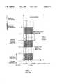
- FIG. 1is a prior art diagram of the readout of a page of even height showing that characters can not be read out along a row in burst mode if the words were read in along columns.
- FIG. 2is a prior art diagram of the readout of a page of even width showing that characters can not be read out along a column in burst mode if the words were read in along rows.
- FIG. 3is a diagram showing the checkerboard pattern where images can be read out along columns or rows in burst mode.
- FIG. 4is a diagram describing data swapping.
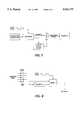
- FIG. 5is a block diagram of a system including a page buffer memory in which this invention may be used.
- FIG. 6is a timing diagram for the circuit of FIG. 5.
- FIG. 7is a block diagram of a circuit for swapping data between a character generator and the memory.
- FIG. 8is a block diagram of a circuit for swapping the least significant bit of the address lines during the loading of data into memory.
- Page buffersare usually implemented from DRAM when a large buffer is required.
- FIG. 1shows a typical prior art system having an even number of locations in each image column. If consecutive accesses are in the same row of the DRAM, that is, if the row address does not change, then the access can utilize the fast page mode, or static column mode, to access DRAM memory, resulting in much better throughput than would result from a series of single accesses.
- the memorycan be divided into two banks of memory, an even bank and an odd bank, so that the two memory banks can be accessed in interleaved fast page mode. When one bank precharges, the other bank can be accessed.
- the interleaved fast page mode of two banks of memorycan achieve one data word access per clock cycle maximum throughput.
- the image page buffercan be loaded with character image data so that either the bytes alternate between odd and even banks in the vertical direction, as in FIG. 1, or in the horizontal direction, as in FIG. 2.
- an attempt to read along a rowwill not result in alternate odd and even accesses
- an attempt to read along a columnwill not result in alternate odd and even accesses.
- both rows and columnscan not be accessed at full speed since, in neither case, do the words alternate between the odd and even memory banks.
- the addresses of the consecutive data words along the fast scan directionare different by one and the adjacent words along the horizontal direction are different by the page height, which in this case is an even number.
- the consecutive data in the fast scan directionfalls into different banks.
- the maximum throughputcan be achieved by alternate accessing of even and odd banks using interleaved fast page mode.
- character imagingusually generates short characters along the slow scan direction (perpendicular to the fast scan direction). One word high characters, for example, would be loaded into only one bank, and therefore can not be interleaved, and the performance of the circuit degrades by half.
- the addresses of the consecutive data along the slow scan directionare different by one and the adjacent word along the fast scan direction is different by the page width.
- the access for short charactersis efficient along the slow scan direction but the access along the fast scan direction becomes a bottleneck.
- the inventionis to configure the odd and even words in the image buffer in a checkerboard pattern so that consecutive data words of the page are in different banks, both vertically and horizontally.
- the memory systemis configured along the fast scan direction so that the address of the consecutive data along the fast scan direction is different by one. However, by setting an odd number for the page height, adjacent locations in the slow scan direction are also in different banks. In this case, the accesses along the fast and slow scan directions can both be interleaved in fast page mode to achieve maximum speed.
- FIG. 3appears to show that when data is read out from a single column, successive words are coming from different rows, and that therefore the memory should not be operating in the page mode.
- successive words in the image columnare most often located in the same row of the device. That is, the device row is so long that several image rows are typically stored in each device row. Therefore, many rows can be read out before an idle cycle is necessary. In the described embodiment, this will happen once for every ten horizontal lines. Therefore, in a four byte high image, for example, this would work out to one idle cycle for every forty lines.
- the sequence of the imaging wordsalternates between the two banks even at the transition between the top word in one column and the lowest word in the next column.
- the character heightis 5 bytes, as shown in FIG. 3, a checkerboard pattern would result if the character image were read in sequentially.
- the sequence of the loading of byteswould result in alternative odd and even bytes within a scanline, but all bytes in the same row would be the same.
- the character heightis 6 bytes, as shown in FIG. 1, a checkerboard would not result if the character image were read in sequentially.
- a character as short as two wordshas this disruption of alternate accesses on every other access.
- Address swappingis designed to improve performance in this special situation when the character height is an even number of words, and the memory height is an odd number of words.
- FIG. 7is a block diagram of a circuit for using this process to transfer data between a character generator and the memory.
- the addressing sequences of each two consecutive accesses on the odd number of scanlines, (1st, 3rd, . . . etc)are swapped to achieve continuous alternate accesses to even and odd memory banks.
- the access sequence of a 4 word high character, see FIG. 4, without address swappingis:
- FIG. 5is a block diagram of a system including a page buffer memory divided into even and odd portions which can be used to implement this invention.
- the page buffer memoryis divided into two halves, the even bank 10 and the odd bank 11.
- the memory control 13sends address and strobe data to the memory banks alternately, and the words output from the two banks are multiplexed by a multiplexer 12 onto a single line and output onto the system bus 14 to the raster output scanner.
- character images from the character generatorare transferred over the system bus 14 through the memory control to the odd and even banks 10, 11.
- the control signals for this circuitare shown in FIG. 6.
- the even memory (column) addressmust be held for two clock cycles, and the even memory control signal (column address strobe or CAS) occurs mainly during the second half of the address cycle.
- the outputoccurs slightly delayed from the strobe.
- Output words 0, 2, 4 and 6are shown.
- the row address line and row address strobe (RAS)are not shown here since it is assumed that the page mode is being used, which implies that the row address is kept constant.
- the odd control signalsare identical except that they are interleaved with the even control signals, so that the alternate odd output words are output in the dead time between even word outputs.
- the system multiplexer 12combines the two data streams to form the system bus data.
Landscapes
- Engineering & Computer Science (AREA)
- Microelectronics & Electronic Packaging (AREA)
- Image Input (AREA)
- Controls And Circuits For Display Device (AREA)
- Memory System (AREA)
- Dram (AREA)
- Storing Facsimile Image Data (AREA)
Abstract
Description
E11, O12, E13, O14, Idle, O21, E22, O23, E24, Idle, E31, O32, . . .
Idle, O12, E11, O14, E13, O21, E22, O23, E24, O32, E31, O34, E33, . . .
Claims (2)
Priority Applications (6)
| Application Number | Priority Date | Filing Date | Title |
|---|---|---|---|
| US08/114,552US5561777A (en) | 1993-08-30 | 1993-08-30 | Process for sequentially reading a page from an image memory in either of two directions |
| EP94305916AEP0640979B1 (en) | 1993-08-30 | 1994-08-10 | Checkerboard image buffer system |
| DE69422101TDE69422101T2 (en) | 1993-08-30 | 1994-08-10 | Checkerboard frame buffer system |
| DE69429936TDE69429936T2 (en) | 1993-08-30 | 1994-08-10 | Operating method of a store |
| EP98114329AEP0887802B1 (en) | 1993-08-30 | 1994-08-10 | Method for operating a memory |
| JP6201787AJPH07168754A (en) | 1993-08-30 | 1994-08-26 | Method for loading and reading of square picture |
Applications Claiming Priority (1)
| Application Number | Priority Date | Filing Date | Title |
|---|---|---|---|
| US08/114,552US5561777A (en) | 1993-08-30 | 1993-08-30 | Process for sequentially reading a page from an image memory in either of two directions |
Publications (1)
| Publication Number | Publication Date |
|---|---|
| US5561777Atrue US5561777A (en) | 1996-10-01 |
Family
ID=22355959
Family Applications (1)
| Application Number | Title | Priority Date | Filing Date |
|---|---|---|---|
| US08/114,552Expired - Fee RelatedUS5561777A (en) | 1993-08-30 | 1993-08-30 | Process for sequentially reading a page from an image memory in either of two directions |
Country Status (4)
| Country | Link |
|---|---|
| US (1) | US5561777A (en) |
| EP (2) | EP0640979B1 (en) |
| JP (1) | JPH07168754A (en) |
| DE (2) | DE69422101T2 (en) |
Cited By (34)
| Publication number | Priority date | Publication date | Assignee | Title |
|---|---|---|---|---|
| US5815169A (en)* | 1995-04-10 | 1998-09-29 | Sharp Kabushiki Kaisha | Frame memory device for graphics allowing simultaneous selection of adjacent horizontal and vertical addresses |
| US6016522A (en)* | 1997-11-13 | 2000-01-18 | Creative Labs, Inc. | System for switching between buffers when receiving bursty audio by computing loop jump indicator plus loop start address for read operations in selected buffer |
| US6018354A (en) | 1994-03-24 | 2000-01-25 | Discovision Associates | Method for accessing banks of DRAM |
| US6125072A (en)* | 1998-07-21 | 2000-09-26 | Seagate Technology, Inc. | Method and apparatus for contiguously addressing a memory system having vertically expanded multiple memory arrays |
| US6247084B1 (en) | 1997-10-08 | 2001-06-12 | Lsi Logic Corporation | Integrated circuit with unified memory system and dual bus architecture |
| US6301649B1 (en)* | 1997-04-07 | 2001-10-09 | Oki Electric Industry Co., Ltd. | Semiconductor circuit with address translation circuit that enables quick serial access in row or column directions |
| US20020109699A1 (en)* | 2001-02-15 | 2002-08-15 | Mark Champion | Pixel pages optimized for GLV |
| US20020109692A1 (en)* | 2001-02-15 | 2002-08-15 | Sony Corporation | Dynamic buffer pages |
| US20020109690A1 (en)* | 2001-02-15 | 2002-08-15 | Mark Champion | Checkerboard buffer using memory bank alternation |
| US20020109792A1 (en)* | 2001-02-15 | 2002-08-15 | Mark Champion | Two-dimensional buffer pages using memory bank alternation |
| US20020109694A1 (en)* | 2001-02-15 | 2002-08-15 | Mark Champion | Checkerboard buffer using two-dimensional buffer pages and using bit-field addressing |
| US20020110351A1 (en)* | 2001-02-15 | 2002-08-15 | Mark Champion | Checkerboard buffer |
| US20020110030A1 (en)* | 2001-02-15 | 2002-08-15 | Mark Champion | Swapped Pixel pages |
| US20020109693A1 (en)* | 2001-02-15 | 2002-08-15 | Mark Champion | Checkerboard buffer using two-dimensional buffer pages |
| US20020109695A1 (en)* | 2001-02-15 | 2002-08-15 | Mark Champion | Checkerboard buffer using two-dimensional buffer pages and using state addressing |
| US20020109689A1 (en)* | 2001-02-15 | 2002-08-15 | Mark Champion | Checkerboard buffer using sequential memory locations |
| US20020109791A1 (en)* | 2001-02-15 | 2002-08-15 | Mark Champion | Two-dimensional buffer pages |
| US20020109696A1 (en)* | 2001-02-15 | 2002-08-15 | Mark Champion | Checkerboard buffer using two-dimensional buffer pages and using memory bank alternation |
| US20020109698A1 (en)* | 2001-02-15 | 2002-08-15 | Mark Champion | Checkerboard buffer using memory blocks |
| US20020109691A1 (en)* | 2001-02-15 | 2002-08-15 | Mark Champion | Two-dimensional buffer pages using state addressing |
| US20020113904A1 (en)* | 2001-02-15 | 2002-08-22 | Mark Champion | Two-dimensional buffer pages using bit-field addressing |
| US20020130876A1 (en)* | 2001-02-15 | 2002-09-19 | Sony Corporation, A Japanese Corporation | Pixel pages using combined addressing |
| US20020149596A1 (en)* | 2001-02-15 | 2002-10-17 | Mark Champion | Checkerboard buffer using more than two memory devices |
| US20030058368A1 (en)* | 2001-09-24 | 2003-03-27 | Mark Champion | Image warping using pixel pages |
| US6599152B1 (en) | 2000-03-20 | 2003-07-29 | 3Com Corporation | Contact pin design for a modular jack |
| US20030151609A1 (en)* | 2002-02-14 | 2003-08-14 | Mark Champion | Multi-sequence burst accessing for SDRAM |
| US20030169278A1 (en)* | 2002-03-06 | 2003-09-11 | Pere Obrador | Delayed encoding based joint video and still image pipeling with still burst mode |
| US20030222882A1 (en)* | 2002-06-03 | 2003-12-04 | Eric Jeffrey | Method and apparatus for fetching pixel data from memory |
| US20040008281A1 (en)* | 2002-07-15 | 2004-01-15 | Eric Jeffrey | Method and apparatus for flicker filtering interlaced display data |
| US20040114690A1 (en)* | 2002-12-06 | 2004-06-17 | Stephen Gordon | Managing bursts of data |
| US20040260903A1 (en)* | 2003-06-23 | 2004-12-23 | Muraleedhara Navada | Ping-pong buffer system having a buffer to store a subset of data from a data source |
| CN100463511C (en)* | 2003-04-28 | 2009-02-18 | 三星电子株式会社 | Image data processing system and image data reading and writing method |
| US20110087856A1 (en)* | 2009-10-13 | 2011-04-14 | Stmicroelectronics (Rousset) Sas | Memory Device with Serial Protocol and Corresponding Method of Addressing |
| US20120098843A1 (en)* | 2010-10-24 | 2012-04-26 | Chun-Yu Chiu | Apparatus for controlling memory device and related method |
Families Citing this family (1)
| Publication number | Priority date | Publication date | Assignee | Title |
|---|---|---|---|---|
| CN106201363B (en)* | 2016-07-26 | 2023-01-31 | 四川大学 | Memory and storage method for random real-time access to video stream pixel-level data |
Citations (7)
| Publication number | Priority date | Publication date | Assignee | Title |
|---|---|---|---|---|
| US4247920A (en)* | 1979-04-24 | 1981-01-27 | Tektronix, Inc. | Memory access system |
| US4561072A (en)* | 1980-04-04 | 1985-12-24 | Nec Corporation | Memory system handling a plurality of bits as a unit to be processed |
| US4740927A (en)* | 1985-02-13 | 1988-04-26 | International Business Machines Corporation | Bit addressable multidimensional array |
| US4893257A (en)* | 1986-11-10 | 1990-01-09 | International Business Machines Corporation | Multidirectional scan and print capability |
| US4926386A (en)* | 1986-12-29 | 1990-05-15 | Park Jong W | Memory system for image processing having address calculating circuitry permitting simultaneous access to block horizontal sequence and vertical sequence subarrays of an array of data |
| US5052046A (en)* | 1988-05-19 | 1991-09-24 | Hitachi, Ltd. | Image processing method and apparatus therefor |
| US5361339A (en)* | 1992-05-04 | 1994-11-01 | Xerox Corporation | Circuit for fast page mode addressing of a RAM with multiplexed row and column address lines |
Family Cites Families (3)
| Publication number | Priority date | Publication date | Assignee | Title |
|---|---|---|---|---|
| DE3015125A1 (en)* | 1980-04-19 | 1981-10-22 | Ibm Deutschland Gmbh, 7000 Stuttgart | DEVICE FOR STORING AND DISPLAYING GRAPHIC INFORMATION |
| US4818932A (en)* | 1986-09-25 | 1989-04-04 | Tektronix, Inc. | Concurrent memory access system |
| DE3913599C1 (en)* | 1989-04-25 | 1990-01-18 | Fraunhofer-Gesellschaft Zur Foerderung Der Angewandten Forschung Ev, 8000 Muenchen, De | Intermediate image store e.g. for TV transmission - assigns separate control to each video channel for connection to all memory blocks |
- 1993
- 1993-08-30USUS08/114,552patent/US5561777A/ennot_activeExpired - Fee Related
- 1994
- 1994-08-10DEDE69422101Tpatent/DE69422101T2/ennot_activeExpired - Fee Related
- 1994-08-10EPEP94305916Apatent/EP0640979B1/ennot_activeExpired - Lifetime
- 1994-08-10EPEP98114329Apatent/EP0887802B1/ennot_activeExpired - Lifetime
- 1994-08-10DEDE69429936Tpatent/DE69429936T2/ennot_activeExpired - Fee Related
- 1994-08-26JPJP6201787Apatent/JPH07168754A/ennot_activeWithdrawn
Patent Citations (7)
| Publication number | Priority date | Publication date | Assignee | Title |
|---|---|---|---|---|
| US4247920A (en)* | 1979-04-24 | 1981-01-27 | Tektronix, Inc. | Memory access system |
| US4561072A (en)* | 1980-04-04 | 1985-12-24 | Nec Corporation | Memory system handling a plurality of bits as a unit to be processed |
| US4740927A (en)* | 1985-02-13 | 1988-04-26 | International Business Machines Corporation | Bit addressable multidimensional array |
| US4893257A (en)* | 1986-11-10 | 1990-01-09 | International Business Machines Corporation | Multidirectional scan and print capability |
| US4926386A (en)* | 1986-12-29 | 1990-05-15 | Park Jong W | Memory system for image processing having address calculating circuitry permitting simultaneous access to block horizontal sequence and vertical sequence subarrays of an array of data |
| US5052046A (en)* | 1988-05-19 | 1991-09-24 | Hitachi, Ltd. | Image processing method and apparatus therefor |
| US5361339A (en)* | 1992-05-04 | 1994-11-01 | Xerox Corporation | Circuit for fast page mode addressing of a RAM with multiplexed row and column address lines |
Cited By (79)
| Publication number | Priority date | Publication date | Assignee | Title |
|---|---|---|---|---|
| US6018354A (en) | 1994-03-24 | 2000-01-25 | Discovision Associates | Method for accessing banks of DRAM |
| US6297857B1 (en)* | 1994-03-24 | 2001-10-02 | Discovision Associates | Method for accessing banks of DRAM |
| US5815169A (en)* | 1995-04-10 | 1998-09-29 | Sharp Kabushiki Kaisha | Frame memory device for graphics allowing simultaneous selection of adjacent horizontal and vertical addresses |
| US6920536B2 (en) | 1997-04-07 | 2005-07-19 | Oki Electric Industry Co., Ltd. | Method of accessing matrix data with address translation circuit that enables quick serial access in row or column directions |
| US6640295B2 (en) | 1997-04-07 | 2003-10-28 | Oki Electric Industry Co., Ltd. | Semiconductor circuit with address translation circuit that enables quick serial access in row or column directions |
| US20040062122A1 (en)* | 1997-04-07 | 2004-04-01 | Atsushi Takasugi | Method of accessing matrix data with address translation circuit that enables quick serial access in row or column directions |
| US6301649B1 (en)* | 1997-04-07 | 2001-10-09 | Oki Electric Industry Co., Ltd. | Semiconductor circuit with address translation circuit that enables quick serial access in row or column directions |
| US7219200B2 (en) | 1997-04-07 | 2007-05-15 | Oki Electric Industry Co., Ltd. | Method of accessing matrix data with address translation circuit that enables quick serial access in row or column directions |
| US20050226082A1 (en)* | 1997-04-07 | 2005-10-13 | Atsushi Takasugi | Method of accessing matrix data with address translation circuit that enables quick serial access in row or column directions |
| US6247084B1 (en) | 1997-10-08 | 2001-06-12 | Lsi Logic Corporation | Integrated circuit with unified memory system and dual bus architecture |
| US6016522A (en)* | 1997-11-13 | 2000-01-18 | Creative Labs, Inc. | System for switching between buffers when receiving bursty audio by computing loop jump indicator plus loop start address for read operations in selected buffer |
| WO2001006371A1 (en)* | 1998-07-21 | 2001-01-25 | Seagate Technology Llc | Improved memory system apparatus and method |
| GB2368415A (en)* | 1998-07-21 | 2002-05-01 | Seagate Technology Llc | Improved memory system apparatus and method |
| GB2368415B (en)* | 1998-07-21 | 2002-10-30 | Seagate Technology Llc | Improved memory system apparatus and method |
| US6125072A (en)* | 1998-07-21 | 2000-09-26 | Seagate Technology, Inc. | Method and apparatus for contiguously addressing a memory system having vertically expanded multiple memory arrays |
| US6599152B1 (en) | 2000-03-20 | 2003-07-29 | 3Com Corporation | Contact pin design for a modular jack |
| US6768490B2 (en) | 2001-02-15 | 2004-07-27 | Sony Corporation | Checkerboard buffer using more than two memory devices |
| US7046249B2 (en) | 2001-02-15 | 2006-05-16 | Sony Corporation | Swapped pixel pages |
| US20020109689A1 (en)* | 2001-02-15 | 2002-08-15 | Mark Champion | Checkerboard buffer using sequential memory locations |
| US20020109791A1 (en)* | 2001-02-15 | 2002-08-15 | Mark Champion | Two-dimensional buffer pages |
| US20020109696A1 (en)* | 2001-02-15 | 2002-08-15 | Mark Champion | Checkerboard buffer using two-dimensional buffer pages and using memory bank alternation |
| US20020109698A1 (en)* | 2001-02-15 | 2002-08-15 | Mark Champion | Checkerboard buffer using memory blocks |
| US20020109691A1 (en)* | 2001-02-15 | 2002-08-15 | Mark Champion | Two-dimensional buffer pages using state addressing |
| US20020113904A1 (en)* | 2001-02-15 | 2002-08-22 | Mark Champion | Two-dimensional buffer pages using bit-field addressing |
| US20020130876A1 (en)* | 2001-02-15 | 2002-09-19 | Sony Corporation, A Japanese Corporation | Pixel pages using combined addressing |
| US20020149596A1 (en)* | 2001-02-15 | 2002-10-17 | Mark Champion | Checkerboard buffer using more than two memory devices |
| US20020109693A1 (en)* | 2001-02-15 | 2002-08-15 | Mark Champion | Checkerboard buffer using two-dimensional buffer pages |
| US8547384B2 (en)* | 2001-02-15 | 2013-10-01 | Sony Corporation | Checkerboard buffer |
| US20020110030A1 (en)* | 2001-02-15 | 2002-08-15 | Mark Champion | Swapped Pixel pages |
| US7830391B2 (en) | 2001-02-15 | 2010-11-09 | Sony Corporation | Checkerboard buffer using two-dimensional buffer pages |
| US7573483B2 (en) | 2001-02-15 | 2009-08-11 | Sony Corporation, A Japanese Corporation | Dynamic buffer pages |
| US20020110351A1 (en)* | 2001-02-15 | 2002-08-15 | Mark Champion | Checkerboard buffer |
| US7379069B2 (en) | 2001-02-15 | 2008-05-27 | Sony Corporation | Checkerboard buffer using two-dimensional buffer pages |
| US20080049032A1 (en)* | 2001-02-15 | 2008-02-28 | Sony Corporation | Checkerboard buffer using two-dimensional buffer pages |
| US20020109694A1 (en)* | 2001-02-15 | 2002-08-15 | Mark Champion | Checkerboard buffer using two-dimensional buffer pages and using bit-field addressing |
| US20020109699A1 (en)* | 2001-02-15 | 2002-08-15 | Mark Champion | Pixel pages optimized for GLV |
| US6765580B2 (en) | 2001-02-15 | 2004-07-20 | Sony Corporation | Pixel pages optimized for GLV |
| US6765579B2 (en) | 2001-02-15 | 2004-07-20 | Sony Corporation | Pixel pages using combined addressing |
| US20020109792A1 (en)* | 2001-02-15 | 2002-08-15 | Mark Champion | Two-dimensional buffer pages using memory bank alternation |
| US6791557B2 (en) | 2001-02-15 | 2004-09-14 | Sony Corporation | Two-dimensional buffer pages using bit-field addressing |
| US6795079B2 (en) | 2001-02-15 | 2004-09-21 | Sony Corporation | Two-dimensional buffer pages |
| US6801204B2 (en)* | 2001-02-15 | 2004-10-05 | Sony Corporation, A Japanese Corporation | Checkerboard buffer using memory blocks |
| US6803917B2 (en)* | 2001-02-15 | 2004-10-12 | Sony Corporation | Checkerboard buffer using memory bank alternation |
| US20040233206A1 (en)* | 2001-02-15 | 2004-11-25 | Sony Corporation, A Japanese Corporation | Pixel pages optimized for GLV |
| US6828977B2 (en) | 2001-02-15 | 2004-12-07 | Sony Corporation | Dynamic buffer pages |
| US20040246258A1 (en)* | 2001-02-15 | 2004-12-09 | Sony Corporation | Swapped pixel pages |
| US6831649B2 (en) | 2001-02-15 | 2004-12-14 | Sony Corporation | Two-dimensional buffer pages using state addressing |
| US6831650B2 (en)* | 2001-02-15 | 2004-12-14 | Sony Corporation | Checkerboard buffer using sequential memory locations |
| US6831651B2 (en) | 2001-02-15 | 2004-12-14 | Sony Corporation | Checkerboard buffer |
| US7205993B2 (en) | 2001-02-15 | 2007-04-17 | Sony Corporation | Checkerboard buffer using two-dimensional buffer pages and using memory bank alternation |
| US6850241B2 (en) | 2001-02-15 | 2005-02-01 | Sony Corporation | Swapped pixel pages |
| US20050024368A1 (en)* | 2001-02-15 | 2005-02-03 | Xiping Liu | Two dimensional buffer pages |
| US20050057572A1 (en)* | 2001-02-15 | 2005-03-17 | Sony Corporation | Checkerboard buffer |
| US20050104890A1 (en)* | 2001-02-15 | 2005-05-19 | Sony Corporation | Dynamic buffer pages |
| US20020109690A1 (en)* | 2001-02-15 | 2002-08-15 | Mark Champion | Checkerboard buffer using memory bank alternation |
| US7129953B2 (en) | 2001-02-15 | 2006-10-31 | Sony Corporation | Two dimensional buffer pages |
| US20020109692A1 (en)* | 2001-02-15 | 2002-08-15 | Sony Corporation | Dynamic buffer pages |
| US7088369B2 (en) | 2001-02-15 | 2006-08-08 | Sony Corporation | Checkerboard buffer using two-dimensional buffer pages and using bit-field addressing |
| US6992674B2 (en) | 2001-02-15 | 2006-01-31 | Sony Corporation | Checkerboard buffer using two-dimensional buffer pages and using state addressing |
| US7068281B2 (en) | 2001-02-15 | 2006-06-27 | Sony Corporation | Pixel pages optimized for GLV |
| US20020109695A1 (en)* | 2001-02-15 | 2002-08-15 | Mark Champion | Checkerboard buffer using two-dimensional buffer pages and using state addressing |
| US7038691B2 (en) | 2001-02-15 | 2006-05-02 | Sony Corporation | Two-dimensional buffer pages using memory bank alternation |
| US20030058368A1 (en)* | 2001-09-24 | 2003-03-27 | Mark Champion | Image warping using pixel pages |
| US6965980B2 (en) | 2002-02-14 | 2005-11-15 | Sony Corporation | Multi-sequence burst accessing for SDRAM |
| US20030151609A1 (en)* | 2002-02-14 | 2003-08-14 | Mark Champion | Multi-sequence burst accessing for SDRAM |
| US20030169278A1 (en)* | 2002-03-06 | 2003-09-11 | Pere Obrador | Delayed encoding based joint video and still image pipeling with still burst mode |
| US6992707B2 (en) | 2002-03-06 | 2006-01-31 | Hewlett-Packard Development Company, L.P. | Delayed encoding based joint video and still image pipeline with still burst mode |
| US20030222882A1 (en)* | 2002-06-03 | 2003-12-04 | Eric Jeffrey | Method and apparatus for fetching pixel data from memory |
| US6919902B2 (en) | 2002-06-03 | 2005-07-19 | Seiko Epson Corporation | Method and apparatus for fetching pixel data from memory |
| US20040008281A1 (en)* | 2002-07-15 | 2004-01-15 | Eric Jeffrey | Method and apparatus for flicker filtering interlaced display data |
| US7034887B2 (en) | 2002-07-15 | 2006-04-25 | Seiko Epson Corporation | Method and apparatus for flicker filtering interlaced display data |
| US20040114690A1 (en)* | 2002-12-06 | 2004-06-17 | Stephen Gordon | Managing bursts of data |
| CN100463511C (en)* | 2003-04-28 | 2009-02-18 | 三星电子株式会社 | Image data processing system and image data reading and writing method |
| US20040260903A1 (en)* | 2003-06-23 | 2004-12-23 | Muraleedhara Navada | Ping-pong buffer system having a buffer to store a subset of data from a data source |
| US7111093B2 (en)* | 2003-06-23 | 2006-09-19 | Intel Corporation | Ping-pong buffer system having a buffer to store a subset of data from a data source |
| US20110087856A1 (en)* | 2009-10-13 | 2011-04-14 | Stmicroelectronics (Rousset) Sas | Memory Device with Serial Protocol and Corresponding Method of Addressing |
| US8572351B2 (en)* | 2009-10-13 | 2013-10-29 | Stmicroelectronics (Rousset) Sas | Memory device with serial protocol and corresponding method of addressing |
| US20120098843A1 (en)* | 2010-10-24 | 2012-04-26 | Chun-Yu Chiu | Apparatus for controlling memory device and related method |
| US8564603B2 (en)* | 2010-10-24 | 2013-10-22 | Himax Technologies Limited | Apparatus for controlling memory device and related method |
Also Published As
| Publication number | Publication date |
|---|---|
| EP0640979A3 (en) | 1995-08-09 |
| EP0887802A3 (en) | 1999-02-10 |
| JPH07168754A (en) | 1995-07-04 |
| EP0640979A2 (en) | 1995-03-01 |
| DE69429936T2 (en) | 2002-06-20 |
| EP0887802A2 (en) | 1998-12-30 |
| DE69429936D1 (en) | 2002-03-28 |
| EP0640979B1 (en) | 1999-12-15 |
| DE69422101T2 (en) | 2000-04-27 |
| EP0887802B1 (en) | 2002-02-20 |
| DE69422101D1 (en) | 2000-01-20 |
Similar Documents
| Publication | Publication Date | Title |
|---|---|---|
| US5561777A (en) | Process for sequentially reading a page from an image memory in either of two directions | |
| US5924111A (en) | Method and system for interleaving data in multiple memory bank partitions | |
| EP0398511B1 (en) | Video random access memory | |
| EP0398510B1 (en) | Video random access memory | |
| KR930011726A (en) | Multiple serial access memories for feedback systems such as motion compensated television | |
| JPH0512755B2 (en) | ||
| US4845640A (en) | High-speed dual mode graphics memory | |
| JPH0141994B2 (en) | ||
| US5361339A (en) | Circuit for fast page mode addressing of a RAM with multiplexed row and column address lines | |
| US7525577B2 (en) | Image processing apparatus and image processing method | |
| US7231413B2 (en) | Transposition circuit | |
| KR100571435B1 (en) | Synchronous dynamic random access memory architecture for sequential burst mode | |
| JP2000066950A (en) | Semiconductor storage device | |
| US6020904A (en) | High speed signal conversion method and device | |
| JPH06167958A (en) | Memory device | |
| JPS593790A (en) | Storage device using dynamic memory element | |
| JPH1139857A (en) | Memory system and information processing system | |
| KR100297716B1 (en) | Semiconductor memory device having high flexibility in column | |
| JP3288327B2 (en) | Video memory circuit | |
| KR100224797B1 (en) | Frame Buffer Drive | |
| JPS60211690A (en) | Memory circuit | |
| KR100224807B1 (en) | Semiconductor memory device and high speed access method | |
| JPH09231745A (en) | Semiconductor memory device | |
| JPH06324935A (en) | Address generator and address generation system | |
| KR19980062324U (en) | Micro process interface |
Legal Events
| Date | Code | Title | Description |
|---|---|---|---|
| AS | Assignment | Owner name:XEROX CORPORATION, CONNECTICUT Free format text:ASSIGNMENT OF ASSIGNORS INTEREST;ASSIGNORS:KAO, JEAN-SWEY;LUI, JACK C.;RIDER, RONALD E.;REEL/FRAME:006691/0176;SIGNING DATES FROM 19930802 TO 19930804 | |
| FPAY | Fee payment | Year of fee payment:4 | |
| AS | Assignment | Owner name:BANK ONE, NA, AS ADMINISTRATIVE AGENT, ILLINOIS Free format text:SECURITY INTEREST;ASSIGNOR:XEROX CORPORATION;REEL/FRAME:013153/0001 Effective date:20020621 | |
| AS | Assignment | Owner name:JPMORGAN CHASE BANK, AS COLLATERAL AGENT, TEXAS Free format text:SECURITY AGREEMENT;ASSIGNOR:XEROX CORPORATION;REEL/FRAME:015134/0476 Effective date:20030625 Owner name:JPMORGAN CHASE BANK, AS COLLATERAL AGENT,TEXAS Free format text:SECURITY AGREEMENT;ASSIGNOR:XEROX CORPORATION;REEL/FRAME:015134/0476 Effective date:20030625 | |
| REMI | Maintenance fee reminder mailed | ||
| LAPS | Lapse for failure to pay maintenance fees | ||
| STCH | Information on status: patent discontinuation | Free format text:PATENT EXPIRED DUE TO NONPAYMENT OF MAINTENANCE FEES UNDER 37 CFR 1.362 | |
| FP | Lapsed due to failure to pay maintenance fee | Effective date:20041001 | |
| AS | Assignment | Owner name:XEROX CORPORATION, CONNECTICUT Free format text:RELEASE BY SECURED PARTY;ASSIGNOR:JPMORGAN CHASE BANK, N.A. AS SUCCESSOR-IN-INTEREST ADMINISTRATIVE AGENT AND COLLATERAL AGENT TO JPMORGAN CHASE BANK;REEL/FRAME:066728/0193 Effective date:20220822 |