US5559556A - Apparatus for connecting an image sensor and an optical unit to a circuit board so that they are properly aligned - Google Patents
Apparatus for connecting an image sensor and an optical unit to a circuit board so that they are properly alignedDownload PDFInfo
- Publication number
- US5559556A US5559556AUS08/367,238US36723895AUS5559556AUS 5559556 AUS5559556 AUS 5559556AUS 36723895 AUS36723895 AUS 36723895AUS 5559556 AUS5559556 AUS 5559556A
- Authority
- US
- United States
- Prior art keywords
- semiconductor package
- holder
- mounting plate
- sensitive surface
- circuit board
- Prior art date
- Legal status (The legal status is an assumption and is not a legal conclusion. Google has not performed a legal analysis and makes no representation as to the accuracy of the status listed.)
- Expired - Fee Related
Links
- 230000003287optical effectEffects0.000titleclaimsabstractdescription17
- 239000004065semiconductorSubstances0.000claimsabstractdescription40
- 238000005476solderingMethods0.000claimsabstractdescription3
- 238000010276constructionMethods0.000description1
- 230000008030eliminationEffects0.000description1
- 238000003379elimination reactionMethods0.000description1
Images


Classifications
- H—ELECTRICITY
- H04—ELECTRIC COMMUNICATION TECHNIQUE
- H04N—PICTORIAL COMMUNICATION, e.g. TELEVISION
- H04N1/00—Scanning, transmission or reproduction of documents or the like, e.g. facsimile transmission; Details thereof
- H04N1/024—Details of scanning heads ; Means for illuminating the original
- H04N1/028—Details of scanning heads ; Means for illuminating the original for picture information pick-up
- H—ELECTRICITY
- H04—ELECTRIC COMMUNICATION TECHNIQUE
- H04N—PICTORIAL COMMUNICATION, e.g. TELEVISION
- H04N23/00—Cameras or camera modules comprising electronic image sensors; Control thereof
- H04N23/50—Constructional details
- H04N23/54—Mounting of pick-up tubes, electronic image sensors, deviation or focusing coils
Definitions
- the present inventionrelates to an arrangement for am image scanning unit comprising a semiconductor package so arranged as to generate electrical signals corresponding to an image incident upon the light-sensitive surface of the package and so arranged as to be connected by soldering to a circuit board, an optical system arranged in a holder for projecting the image to be scanned onto the aforementioned light-sensitive surface, a mounting plate positioned between the semiconductor package and the circuit board, and devices for joining together the holder and the mounting plate and for ensuring correct mutual alignment between the semiconductor package and the optical system.
- the object of the present inventionis to make available an arrangement of the kind referred to by way of introduction, in which elimination of the above-mentioned disadvantages has been effected and has been made possible in that in order to ensure correct alignment between the optical system and the light-sensitive surface of the semiconductor package in the longitudinal direction of the semiconductor package, the aforementioned devices comprise a projection projecting from the holder in such a way, when the unit is assembled, that it engages between two of the contact legs of the semiconductor package, and that for ensuring correct alignment in the transverse direction of the semiconductor package and in a direction normal to the light-sensitive surface, the aforementioned joining devices comprise snap elements capable of interacting with one another arranged on the holder and on the mounting plate.
- a desired alignment accuracy tolerance between the optical system and the light-sensitive surface of the semiconductor packageis achieved through the characteristic features of the invention in that the location of the holder is achieved by means of the semiconductor package itself or, rather, with two of its contact legs.
- a space-saving, rapid, reliable and simple jointis obtained between the holder and the mounting plate.
- the snap elements in one preferred embodimentare arranged along two lines running parallel to one another and to the longitudinal edges of the semiconductor package and lying in areas close to them.
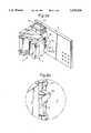
- FIG. 1illustrates an exploded view of the invention in perspective view.
- FIG. 2ashows the arrangement in accordance with the invention installed
- FIG. 2bis a detailed view showing a projection which ensures correct alignment between the light-sensitive surface of a semiconductor package and an optical system, by means of which an image is projected onto the aforementioned surface.
- FIG. 3ashows the arrangement in accordance with the invention shown in FIG. 2a in side view
- FIG. 3bis an enlarged partial view of FIG. 3a, which shows snap elements by means of which a holder for the optical system is fixed to a mounting plate for the holder.
- the designation 1is used in the drawing generally for an image scanning unit comprising a semiconductor package 2 with a light-sensitive surface 2a, a holder 3 for an optical system (not shown in the drawing) for projecting onto the light-sensitive surface 2a an image which is to be scanned, a mounting plate 4 and a circuit board 5.
- the semiconductor packagehas contact legs 2b which carry electrical signals corresponding to the image incident upon the light-sensitive surface 2a when the image scanning unit is being used, and which are intended to be connected in the conventional manner to a conductive pattern on the circuit board 5.
- the contact legs 2bare inserted for this purpose into holes 5a in the circuit board 5 and are soldered in place to the conductive pattern.
- the mounting plate 4is so arranged as to be positioned between the semiconductor package 2 and the circuit board 5 in the space which is conventionally present between a circuit board and a semiconductor package of this kind when it is soldered in place on the circuit board.
- the holder 3exhibits on its surface facing the semiconductor package 2 a recess 3c into which the semiconductor package 2 fits.
- the edges 3cl, 3c2 of the recess 3cform guide edges for the longitudinal edges of the semiconductor package 2.
- the internal surfaces of the snap elements 4a belonging to the mounting plate 4 and facing towards the contact legs 2balso touch corresponding contact legs 2b. Very stable and reliable alignment is thus achieved between the component parts of the arrangement.
- An image scanning unit 1 in accordance with the inventionis installed as follows: first the semiconductor package 2 is attached to the mounting plate 4, in conjunction with which a number of the contact legs 2b of the semiconductor package 2, more specifically those which are situated in association with the snap elements 4a, are caused to pass through transcurrent holes 4b in the mounting plate 4. The rear surface 2c of the semiconductor package 2 facing away from the light-sensitive surface 2a now comes into contact with the top surface 4c of the mounting plate. The semiconductor package 2 together with the mounting plate 4 is then assembled with the circuit board 5, whereupon the contact legs 2b are soldered in place on the circuit board 5 in the conventional manner.
- the holder 3can now be installed. It is essential to make sure that the projection 3a is introduced between two selected contact legs 2b at the same time as the snap elements 3b, 4a are brought into engagement with one another. Once this has occurred, an edge area of the light-sensitive surface 2a will lie against a surface (not shown in the drawing) corresponding to the underside of the holder 3. Direct and accurate alignment of the holder, and thus of the optical system arranged in the holder, relative to the light-sensitive surface is achieved in this way.
Landscapes
- Engineering & Computer Science (AREA)
- Multimedia (AREA)
- Signal Processing (AREA)
- Mechanical Optical Scanning Systems (AREA)
- Facsimile Heads (AREA)
- Solid State Image Pick-Up Elements (AREA)
- Transforming Light Signals Into Electric Signals (AREA)
- Electric Connection Of Electric Components To Printed Circuits (AREA)
- Image Input (AREA)
- Light Receiving Elements (AREA)
Abstract
Description
1. Field of the Invention
The present invention relates to an arrangement for am image scanning unit comprising a semiconductor package so arranged as to generate electrical signals corresponding to an image incident upon the light-sensitive surface of the package and so arranged as to be connected by soldering to a circuit board, an optical system arranged in a holder for projecting the image to be scanned onto the aforementioned light-sensitive surface, a mounting plate positioned between the semiconductor package and the circuit board, and devices for joining together the holder and the mounting plate and for ensuring correct mutual alignment between the semiconductor package and the optical system.
2. Description of the Related Art
An arrangement of this kind is previously disclosed through U.S. Pat. No. 4,594,613. The mounting plate is attached in this case to the holder for the optical system by means of screws and pins, which project outwards from the holder and interact with holes in the mounting plate in order to ensure the desired alignment between the semiconductor package and the optical system. The previously disclosed arrangement has a comparatively bulky construction and uses many detail components which demand a relatively long assembly time; in order to be able to fix the holder to the mounting plate with screws, or vice versa, openings are also required in the actual circuit board. Ensuring that the holder is correctly aligned relative to the semiconductor package, as briefly described above, means that the accuracy of the alignment may be jeopardized.
The object of the present invention is to make available an arrangement of the kind referred to by way of introduction, in which elimination of the above-mentioned disadvantages has been effected and has been made possible in that in order to ensure correct alignment between the optical system and the light-sensitive surface of the semiconductor package in the longitudinal direction of the semiconductor package, the aforementioned devices comprise a projection projecting from the holder in such a way, when the unit is assembled, that it engages between two of the contact legs of the semiconductor package, and that for ensuring correct alignment in the transverse direction of the semiconductor package and in a direction normal to the light-sensitive surface, the aforementioned joining devices comprise snap elements capable of interacting with one another arranged on the holder and on the mounting plate.
A desired alignment accuracy tolerance between the optical system and the light-sensitive surface of the semiconductor package is achieved through the characteristic features of the invention in that the location of the holder is achieved by means of the semiconductor package itself or, rather, with two of its contact legs. In addition, a space-saving, rapid, reliable and simple joint is obtained between the holder and the mounting plate.
In accordance with one particular characteristic of the invention, the snap elements in one preferred embodiment are arranged along two lines running parallel to one another and to the longitudinal edges of the semiconductor package and lying in areas close to them.
The invention is described in greater detail below with reference to the accompanying drawing, in which FIG. 1 illustrates an exploded view of the invention in perspective view. FIG. 2ashows the arrangement in accordance with the invention installed, and FIG. 2b is a detailed view showing a projection which ensures correct alignment between the light-sensitive surface of a semiconductor package and an optical system, by means of which an image is projected onto the aforementioned surface. FIG. 3a shows the arrangement in accordance with the invention shown in FIG. 2a in side view, and FIG. 3b is an enlarged partial view of FIG. 3a, which shows snap elements by means of which a holder for the optical system is fixed to a mounting plate for the holder.
The designation 1 is used in the drawing generally for an image scanning unit comprising asemiconductor package 2 with a light-sensitive surface 2a, aholder 3 for an optical system (not shown in the drawing) for projecting onto the light-sensitive surface 2a an image which is to be scanned, amounting plate 4 and acircuit board 5.
The semiconductor package hascontact legs 2b which carry electrical signals corresponding to the image incident upon the light-sensitive surface 2a when the image scanning unit is being used, and which are intended to be connected in the conventional manner to a conductive pattern on thecircuit board 5. Thecontact legs 2b are inserted for this purpose intoholes 5a in thecircuit board 5 and are soldered in place to the conductive pattern. Themounting plate 4 is so arranged as to be positioned between thesemiconductor package 2 and thecircuit board 5 in the space which is conventionally present between a circuit board and a semiconductor package of this kind when it is soldered in place on the circuit board.
Rapid and reliable joining of theholder 3 to the mounting plate and, at the same time, accurate alignment of the optical system relative to the light-sensitive surface 2a in the transverse direction of thesemiconductor package 2 and in a direction normal to thesurface 2a are achieved in accordance with the invention by means ofsnap elements holder 3 and on themounting plate 4 and preferably integral with them. The manner in which thesesnap elements
Theholder 3 exhibits on its surface facing thesemiconductor package 2 arecess 3c into which the semiconductor package 2 fits. When thepackage 2 is introduced into therecess 3c and rests against its bottom, the edges 3cl, 3c2 of therecess 3c form guide edges for the longitudinal edges of thesemiconductor package 2. When the arrangement is installed, the internal surfaces of thesnap elements 4a belonging to themounting plate 4 and facing towards thecontact legs 2b also touchcorresponding contact legs 2b. Very stable and reliable alignment is thus achieved between the component parts of the arrangement.
An image scanning unit 1 in accordance with the invention is installed as follows: first thesemiconductor package 2 is attached to themounting plate 4, in conjunction with which a number of thecontact legs 2b of thesemiconductor package 2, more specifically those which are situated in association with thesnap elements 4a, are caused to pass throughtranscurrent holes 4b in themounting plate 4. The rear surface 2c of thesemiconductor package 2 facing away from the light-sensitive surface 2a now comes into contact with the top surface 4c of the mounting plate. Thesemiconductor package 2 together with themounting plate 4 is then assembled with thecircuit board 5, whereupon thecontact legs 2b are soldered in place on thecircuit board 5 in the conventional manner.
Theholder 3 can now be installed. It is essential to make sure that theprojection 3a is introduced between two selectedcontact legs 2b at the same time as thesnap elements sensitive surface 2a will lie against a surface (not shown in the drawing) corresponding to the underside of theholder 3. Direct and accurate alignment of the holder, and thus of the optical system arranged in the holder, relative to the light-sensitive surface is achieved in this way.
Claims (4)
1. An arrangement for an image scanning unit comprising:
a semiconductor package, so arranged as to generate electrical signals corresponding to an image incident upon a light-sensitive surface of the package, and so arranged as to be connected to a circuit board by soldering its contact legs to the circuit board, the semiconductor package extending generally in a first, longitudinal, direction and a second, transverse, direction, and the light-sensitive surface extending in said longitudinal and transverse directions;
an optical system arranged in a holder for projecting the image to be scanned onto the light-sensitive surface;
a mounting plate positioned between the semiconductor package and the circuit board, and
devices for joining together the holder and the mounting plate and ensuring correct mutual alignment between the semiconductor package and the optical system;
wherein, for ensuring correct alignment between the optical system and the light-sensitive surface of the semiconductor package in the longitudinal direction of the semiconductor package, said joining devices comprise a projection projecting from the holder in such a way that, when the unit is assembled, it engages between two of the contact legs of the semiconductor package;
and wherein, for ensuring correct alignment in the transverse direction of the semiconductor package and in a direction normal to the light-sensitive surface, said joining devices comprise snap elements, capable of interacting with one another, arranged on the holder and on the mounting plate.
2. An arrangement as claimed in claim 1, wherein the holder exhibits, on its surface facing the semiconductor package, a recess into which the package fits, the edges of which recess form guide edges for edges of the semiconductor package extending in the longitudinal direction.
3. An arrangement as claimed in claim 1, wherein the holder exhibits, on its surface towards the semiconductor package, a recess into which the package fits, the edges of which recess form guide edges for the longitudinal edges of the semiconductor package.
4. An arrangement as claimed in claim 1, wherein the surfaces of the snap elements arranged on the mounting plate and facing towards the contact legs also touch corresponding contact legs.
Applications Claiming Priority (3)
| Application Number | Priority Date | Filing Date | Title |
|---|---|---|---|
| SE9202016ASE9202016L (en) | 1992-06-30 | 1992-06-30 | Device at an image reading unit |
| SE9202016.3 | 1992-06-30 | ||
| PCT/SE1993/000529WO1994000883A1 (en) | 1992-06-30 | 1993-06-15 | Arrangement for an image scanning unit |
Publications (1)
| Publication Number | Publication Date |
|---|---|
| US5559556Atrue US5559556A (en) | 1996-09-24 |
Family
ID=20386657
Family Applications (1)
| Application Number | Title | Priority Date | Filing Date |
|---|---|---|---|
| US08/367,238Expired - Fee RelatedUS5559556A (en) | 1992-06-30 | 1993-06-15 | Apparatus for connecting an image sensor and an optical unit to a circuit board so that they are properly aligned |
Country Status (7)
| Country | Link |
|---|---|
| US (1) | US5559556A (en) |
| EP (1) | EP0648376B1 (en) |
| DE (1) | DE69314955T2 (en) |
| ES (1) | ES2110099T3 (en) |
| SE (1) | SE9202016L (en) |
| WO (1) | WO1994000883A1 (en) |
| ZA (1) | ZA934575B (en) |
Cited By (27)
| Publication number | Priority date | Publication date | Assignee | Title |
|---|---|---|---|---|
| US5828409A (en)* | 1995-06-30 | 1998-10-27 | Eastman Kodak Company | Film scanner mount assembly for a solid state sensor |
| DE19838362C1 (en)* | 1998-08-18 | 2000-02-10 | Deutsch Zentr Luft & Raumfahrt | Focal plane plate for high resolution CCD camera e.g. aircraft flight camera |
| US6117193A (en)* | 1999-10-20 | 2000-09-12 | Amkor Technology, Inc. | Optical sensor array mounting and alignment |
| US20030025824A1 (en)* | 1997-05-23 | 2003-02-06 | Koji Ishikawa | Image pickup device incorporating a position defining member |
| DE19932065C2 (en)* | 1998-08-18 | 2003-06-26 | Deutsch Zentr Luft & Raumfahrt | Focal plane plate for a high-resolution camera with light-sensitive semiconductor sensors |
| US6710945B1 (en) | 2002-06-03 | 2004-03-23 | Amkor Technology, Inc. | Injection molded lens-barrel assembly and method for fabricating lens-barrel and mount assemblies |
| US20040252195A1 (en)* | 2003-06-13 | 2004-12-16 | Jih-Yung Lu | Method of aligning lens and sensor of camera |
| US20050007637A1 (en)* | 2003-07-07 | 2005-01-13 | Sheng-Chung Tsai | Method for adjusting a scanning module |
| US6861720B1 (en) | 2001-08-29 | 2005-03-01 | Amkor Technology, Inc. | Placement template and method for placing optical dies |
| US20090180013A1 (en)* | 2008-01-10 | 2009-07-16 | Sharp Kabushiki Kaisha | Solid image capture device and electronic device incorporating same |
| US8130315B2 (en) | 2008-02-13 | 2012-03-06 | Sharp Kabushiki Kaisha | Solid image capture device and electronic device incorporating same |
| US8542451B2 (en) | 2009-03-25 | 2013-09-24 | Magna Electronics Inc. | Vehicular camera and lens assembly |
| US8553131B2 (en) | 2010-06-03 | 2013-10-08 | Bendix Commercial Vehicle Systems Llc | Six-axis mount |
| US9451138B2 (en) | 2013-11-07 | 2016-09-20 | Magna Electronics Inc. | Camera for vehicle vision system |
| US9749509B2 (en) | 2014-03-13 | 2017-08-29 | Magna Electronics Inc. | Camera with lens for vehicle vision system |
| US20180020140A1 (en)* | 2015-02-05 | 2018-01-18 | Conti Temic Microelectronic Gmbh | Camera module and method for the production thereof |
| US10142532B2 (en) | 2016-04-08 | 2018-11-27 | Magna Electronics Inc. | Camera for vehicle vision system |
| US10230875B2 (en) | 2016-04-14 | 2019-03-12 | Magna Electronics Inc. | Camera for vehicle vision system |
| US10237456B2 (en) | 2016-08-22 | 2019-03-19 | Magna Electronics Inc. | Vehicle camera assembly process |
| US10250004B2 (en) | 2015-11-05 | 2019-04-02 | Magna Electronics Inc. | Method of forming a connector for an electrical cable for electrically connecting to a camera of a vehicle |
| US10351072B2 (en) | 2015-11-05 | 2019-07-16 | Magna Electronics Inc. | Vehicle camera with modular construction |
| US10462375B2 (en) | 2011-08-02 | 2019-10-29 | Magna Electronics Inc. | Exterior viewing camera module for vehicle vision system |
| US10523853B2 (en) | 2008-10-16 | 2019-12-31 | Magna Electronics Inc. | Method of assembling camera for vehicular applications |
| US10560613B2 (en) | 2015-11-05 | 2020-02-11 | Magna Electronics Inc. | Vehicle camera with modular construction |
| US10576909B2 (en) | 2011-04-20 | 2020-03-03 | Magna Electronics Inc. | Vehicular vision system with windshield mounted camera |
| US10787125B2 (en) | 2011-08-02 | 2020-09-29 | Magna Electronics Inc. | Vehicular camera system |
| US12328491B1 (en) | 2009-03-25 | 2025-06-10 | Magna Electronics Inc. | Vehicular camera and lens assembly |
Families Citing this family (1)
| Publication number | Priority date | Publication date | Assignee | Title |
|---|---|---|---|---|
| KR100404398B1 (en)* | 2001-10-26 | 2003-11-05 | 엔프라니 주식회사 | Composition and method for prevention and improvement of wrinkle |
Citations (5)
| Publication number | Priority date | Publication date | Assignee | Title |
|---|---|---|---|---|
| US4594613A (en)* | 1982-02-16 | 1986-06-10 | Canon Kabushiki Kaisha | Solid-state imaging device assembly |
| US4803557A (en)* | 1988-01-11 | 1989-02-07 | Eastman Kodak Company | Adjustable mount for image sensor |
| US5153734A (en)* | 1989-11-30 | 1992-10-06 | Fuji Photo Film Co., Ltd. | Solid state image pickup device mounting structure |
| US5274456A (en)* | 1987-12-28 | 1993-12-28 | Hitachi, Ltd. | Semiconductor device and video camera unit using it and their manufacturing method |
| US5444485A (en)* | 1990-06-04 | 1995-08-22 | Fuji Photo Film Co., Ltd. | Camera with turret lens and solid state image sensor |
Family Cites Families (2)
| Publication number | Priority date | Publication date | Assignee | Title |
|---|---|---|---|---|
| JPS574657A (en)* | 1980-06-11 | 1982-01-11 | Hitachi Ltd | Position control and attachment of solid state scanning element |
| JPS5927663U (en)* | 1982-08-12 | 1984-02-21 | キヤノン株式会社 | image reading device |
- 1992
- 1992-06-30SESE9202016Apatent/SE9202016L/ennot_activeIP Right Cessation
- 1993
- 1993-06-15ESES93915056Tpatent/ES2110099T3/ennot_activeExpired - Lifetime
- 1993-06-15USUS08/367,238patent/US5559556A/ennot_activeExpired - Fee Related
- 1993-06-15DEDE69314955Tpatent/DE69314955T2/ennot_activeExpired - Fee Related
- 1993-06-15EPEP93915056Apatent/EP0648376B1/ennot_activeExpired - Lifetime
- 1993-06-15WOPCT/SE1993/000529patent/WO1994000883A1/enactiveIP Right Grant
- 1993-06-25ZAZA934575Apatent/ZA934575B/enunknown
Patent Citations (5)
| Publication number | Priority date | Publication date | Assignee | Title |
|---|---|---|---|---|
| US4594613A (en)* | 1982-02-16 | 1986-06-10 | Canon Kabushiki Kaisha | Solid-state imaging device assembly |
| US5274456A (en)* | 1987-12-28 | 1993-12-28 | Hitachi, Ltd. | Semiconductor device and video camera unit using it and their manufacturing method |
| US4803557A (en)* | 1988-01-11 | 1989-02-07 | Eastman Kodak Company | Adjustable mount for image sensor |
| US5153734A (en)* | 1989-11-30 | 1992-10-06 | Fuji Photo Film Co., Ltd. | Solid state image pickup device mounting structure |
| US5444485A (en)* | 1990-06-04 | 1995-08-22 | Fuji Photo Film Co., Ltd. | Camera with turret lens and solid state image sensor |
Cited By (79)
| Publication number | Priority date | Publication date | Assignee | Title |
|---|---|---|---|---|
| US5828409A (en)* | 1995-06-30 | 1998-10-27 | Eastman Kodak Company | Film scanner mount assembly for a solid state sensor |
| US20030025824A1 (en)* | 1997-05-23 | 2003-02-06 | Koji Ishikawa | Image pickup device incorporating a position defining member |
| US6654064B2 (en)* | 1997-05-23 | 2003-11-25 | Canon Kabushiki Kaisha | Image pickup device incorporating a position defining member |
| US6750488B1 (en) | 1998-08-18 | 2004-06-15 | Deutsches Zentrum für Luft- und Raumfahrt e.V. | Focal plane plate for a high-resolution camera with light-sensitive semiconductor sensors |
| DE19838362C1 (en)* | 1998-08-18 | 2000-02-10 | Deutsch Zentr Luft & Raumfahrt | Focal plane plate for high resolution CCD camera e.g. aircraft flight camera |
| DE19932065C2 (en)* | 1998-08-18 | 2003-06-26 | Deutsch Zentr Luft & Raumfahrt | Focal plane plate for a high-resolution camera with light-sensitive semiconductor sensors |
| US6117193A (en)* | 1999-10-20 | 2000-09-12 | Amkor Technology, Inc. | Optical sensor array mounting and alignment |
| US6861720B1 (en) | 2001-08-29 | 2005-03-01 | Amkor Technology, Inc. | Placement template and method for placing optical dies |
| US6710945B1 (en) | 2002-06-03 | 2004-03-23 | Amkor Technology, Inc. | Injection molded lens-barrel assembly and method for fabricating lens-barrel and mount assemblies |
| US7071966B2 (en)* | 2003-06-13 | 2006-07-04 | Benq Corporation | Method of aligning lens and sensor of camera |
| US20040252195A1 (en)* | 2003-06-13 | 2004-12-16 | Jih-Yung Lu | Method of aligning lens and sensor of camera |
| US20050007637A1 (en)* | 2003-07-07 | 2005-01-13 | Sheng-Chung Tsai | Method for adjusting a scanning module |
| US7483182B2 (en)* | 2003-07-07 | 2009-01-27 | Avision Inc. | Method for adjusting a scanning module |
| US8269883B2 (en)* | 2008-01-10 | 2012-09-18 | Sharp Kabushiki Kaisha | Solid image capture device and electronic device incorporating same |
| US20090180013A1 (en)* | 2008-01-10 | 2009-07-16 | Sharp Kabushiki Kaisha | Solid image capture device and electronic device incorporating same |
| US8130315B2 (en) | 2008-02-13 | 2012-03-06 | Sharp Kabushiki Kaisha | Solid image capture device and electronic device incorporating same |
| US12206976B2 (en) | 2008-10-16 | 2025-01-21 | Magna Electronics | Vehicular camera module |
| US11785327B2 (en) | 2008-10-16 | 2023-10-10 | Magna Electronics Inc. | Vehicular camera module |
| US11617021B2 (en) | 2008-10-16 | 2023-03-28 | Magna Electronics Inc. | Vehicular camera module |
| US11240415B2 (en) | 2008-10-16 | 2022-02-01 | Magna Electronics Inc. | Vehicular camera with metallic housing |
| US10523853B2 (en) | 2008-10-16 | 2019-12-31 | Magna Electronics Inc. | Method of assembling camera for vehicular applications |
| US10979611B2 (en) | 2008-10-16 | 2021-04-13 | Magna Electronics Inc. | Method of assembling camera for vehicular applications |
| US11146713B2 (en) | 2009-03-25 | 2021-10-12 | Magna Electronics Inc. | Vehicular camera and lens assembly |
| US11457134B2 (en) | 2009-03-25 | 2022-09-27 | Magna Electronics Inc. | Vehicular camera and lens assembly |
| US12328491B1 (en) | 2009-03-25 | 2025-06-10 | Magna Electronics Inc. | Vehicular camera and lens assembly |
| US10917548B2 (en) | 2009-03-25 | 2021-02-09 | Magna Electronics Inc. | Vehicular camera and lens assembly and method of manufacturing same |
| US10015377B2 (en) | 2009-03-25 | 2018-07-03 | Magna Electronics Inc. | Vehicular camera and lens assembly and method of manufacturing same |
| US8542451B2 (en) | 2009-03-25 | 2013-09-24 | Magna Electronics Inc. | Vehicular camera and lens assembly |
| US12035027B2 (en) | 2009-03-25 | 2024-07-09 | Magna Electronics Inc. | Vehicular camera and lens assembly |
| US9338334B2 (en) | 2009-03-25 | 2016-05-10 | Magna Electronics Inc. | Vehicular camera and lens assembly |
| US10708476B2 (en) | 2009-03-25 | 2020-07-07 | Magna Electronics Inc. | Vehicular camera and lens assembly and method of manufacturing same |
| US9277104B2 (en) | 2009-03-25 | 2016-03-01 | Magna Electronics Inc. | Vehicular camera and lens assembly and method of manufacturing same |
| US10270949B2 (en) | 2009-03-25 | 2019-04-23 | Magna Electronics Inc. | Vehicular camera and lens assembly |
| US8553131B2 (en) | 2010-06-03 | 2013-10-08 | Bendix Commercial Vehicle Systems Llc | Six-axis mount |
| US11667252B2 (en) | 2011-04-20 | 2023-06-06 | Magna Electronics Inc. | Vehicular vision system with windshield mounted camera |
| US11427136B2 (en) | 2011-04-20 | 2022-08-30 | Magna Electronics Inc. | Vehicular vision system with windshield mounted camera |
| US11975660B2 (en) | 2011-04-20 | 2024-05-07 | Magna Electronics Inc. | Vehicular vision system with windshield mounted camera |
| US11052834B2 (en) | 2011-04-20 | 2021-07-06 | Magna Electronics Inc. | Vehicular vision system with windshield mounted camera |
| US12246657B2 (en) | 2011-04-20 | 2025-03-11 | Magna Electronics Inc. | Vehicular vision system with windshield mounted camera |
| US10857953B1 (en) | 2011-04-20 | 2020-12-08 | Magna Electronics Inc. | Vehicular vision system with windshield mounted camera |
| US10793086B2 (en) | 2011-04-20 | 2020-10-06 | Magna Electronics Inc. | Vehicular vision system with windshield mounted camera |
| US10576909B2 (en) | 2011-04-20 | 2020-03-03 | Magna Electronics Inc. | Vehicular vision system with windshield mounted camera |
| US11718228B2 (en) | 2011-08-02 | 2023-08-08 | Magna Electronics Inc. | Vehicular camera system |
| US10462375B2 (en) | 2011-08-02 | 2019-10-29 | Magna Electronics Inc. | Exterior viewing camera module for vehicle vision system |
| US11758274B2 (en) | 2011-08-02 | 2023-09-12 | Magna Electronics Inc. | Vehicular camera module |
| US12279045B2 (en) | 2011-08-02 | 2025-04-15 | Magna Electronics Inc. | Vehicular camera module |
| US11997392B2 (en) | 2011-08-02 | 2024-05-28 | Magna Electronics Inc. | Vehicular camera module |
| US10771708B2 (en) | 2011-08-02 | 2020-09-08 | Magna Electronics Inc. | Exterior viewing camera module for vehicle vision system |
| US10787125B2 (en) | 2011-08-02 | 2020-09-29 | Magna Electronics Inc. | Vehicular camera system |
| US12109951B2 (en) | 2011-08-02 | 2024-10-08 | Magna Electronics Inc. | Vehicular camera system |
| US12162412B2 (en) | 2011-08-02 | 2024-12-10 | Magna Electronics Inc. | Vehicular camera system |
| US11212453B2 (en) | 2011-08-02 | 2021-12-28 | Magna Electroncs Inc. | Camera module for vehicular driving assist system |
| US9497368B1 (en) | 2013-11-07 | 2016-11-15 | Magna Electronics Inc. | Method of assembling camera for vehicle vision system |
| US9635230B2 (en) | 2013-11-07 | 2017-04-25 | Magna Electronics Inc. | Method of assembling camera for vehicle vision system |
| US10674053B2 (en) | 2013-11-07 | 2020-06-02 | Magna Electronics Inc. | Vehicular camera with adhesively bonded construction |
| US11108939B2 (en) | 2013-11-07 | 2021-08-31 | Magna Electronics Inc. | Vehicular camera with adhesively bonded construction |
| US9451138B2 (en) | 2013-11-07 | 2016-09-20 | Magna Electronics Inc. | Camera for vehicle vision system |
| US9883088B2 (en) | 2013-11-07 | 2018-01-30 | Magna Electronics Inc. | Method of assembling camera for vehicle vision system |
| US10419652B2 (en) | 2013-11-07 | 2019-09-17 | Magna Electronics Inc. | Vehicular camera with adhesively bonded construction |
| US11622168B2 (en) | 2013-11-07 | 2023-04-04 | Magna Electronics Inc. | Vehicular camera with adhesively bonded construction |
| US12273611B2 (en) | 2013-11-07 | 2025-04-08 | Magna Electronics Inc. | Vehicular camera with adhesively bonded construction |
| US10264168B2 (en) | 2013-11-07 | 2019-04-16 | Magna Electronics Inc. | Method of assembling camera for vehicle vision system |
| US10757305B1 (en) | 2013-11-07 | 2020-08-25 | Magna Electronics Inc. | Vehicular camera with adhesively bonded construction |
| US9749509B2 (en) | 2014-03-13 | 2017-08-29 | Magna Electronics Inc. | Camera with lens for vehicle vision system |
| US10154184B2 (en)* | 2015-02-05 | 2018-12-11 | Conti Temic Microelectronic Gmbh | Camera module and method for the production thereof |
| US20180020140A1 (en)* | 2015-02-05 | 2018-01-18 | Conti Temic Microelectronic Gmbh | Camera module and method for the production thereof |
| US10965846B2 (en) | 2015-11-05 | 2021-03-30 | Magna Electronics Inc. | Method of assembling a camera for vehicular vision system |
| US10250004B2 (en) | 2015-11-05 | 2019-04-02 | Magna Electronics Inc. | Method of forming a connector for an electrical cable for electrically connecting to a camera of a vehicle |
| US11528391B2 (en) | 2015-11-05 | 2022-12-13 | Magna Electronics Inc. | Vehicular camera module |
| US10351072B2 (en) | 2015-11-05 | 2019-07-16 | Magna Electronics Inc. | Vehicle camera with modular construction |
| US11245819B2 (en) | 2015-11-05 | 2022-02-08 | Magna Electronics Inc. | Vehicular camera module |
| US10477083B2 (en) | 2015-11-05 | 2019-11-12 | Magna Electronics Inc. | Camera for vehicular vision system |
| US10560613B2 (en) | 2015-11-05 | 2020-02-11 | Magna Electronics Inc. | Vehicle camera with modular construction |
| US10604084B2 (en) | 2015-11-05 | 2020-03-31 | Magna Electronics Inc. | Vehicle camera with modular construction |
| US10367984B2 (en) | 2016-04-08 | 2019-07-30 | Magna Electronics Inc. | Method of forming camera module for vehicular vision system |
| US10142532B2 (en) | 2016-04-08 | 2018-11-27 | Magna Electronics Inc. | Camera for vehicle vision system |
| US10694090B2 (en) | 2016-04-08 | 2020-06-23 | Magna Electronics Inc. | Method of forming camera module for vehicular vision system |
| US10230875B2 (en) | 2016-04-14 | 2019-03-12 | Magna Electronics Inc. | Camera for vehicle vision system |
| US10237456B2 (en) | 2016-08-22 | 2019-03-19 | Magna Electronics Inc. | Vehicle camera assembly process |
Also Published As
| Publication number | Publication date |
|---|---|
| ES2110099T3 (en) | 1998-02-01 |
| SE9202016D0 (en) | 1992-06-30 |
| ZA934575B (en) | 1994-01-31 |
| EP0648376A1 (en) | 1995-04-19 |
| DE69314955D1 (en) | 1997-12-04 |
| DE69314955T2 (en) | 1998-04-30 |
| SE469864B (en) | 1993-09-27 |
| SE9202016L (en) | 1993-09-27 |
| EP0648376B1 (en) | 1997-10-29 |
| WO1994000883A1 (en) | 1994-01-06 |
Similar Documents
| Publication | Publication Date | Title |
|---|---|---|
| US5559556A (en) | Apparatus for connecting an image sensor and an optical unit to a circuit board so that they are properly aligned | |
| JP3594439B2 (en) | camera | |
| US6156587A (en) | Method of attaching solid state imaging device | |
| JP2849639B2 (en) | Imaging device | |
| US5218462A (en) | Image sensor module for handy-type image input apparatus | |
| US5828409A (en) | Film scanner mount assembly for a solid state sensor | |
| JP2000069336A (en) | Mount structure for image pickup device | |
| JPH02172166A (en) | Mounting structure between electrical connector and printed wiring board | |
| JPH08293687A (en) | Method of manufacturing shielded electric product with connector for external connection and the product | |
| JPH0570955B2 (en) | ||
| JP2000252652A (en) | Board holder for control apparatus | |
| JP3063414B2 (en) | Electronics | |
| JPH05236306A (en) | Video camera | |
| JPH0432798Y2 (en) | ||
| JP2569214Y2 (en) | Flexible board fixing mechanism | |
| JPH05284412A (en) | Optical block for camera | |
| JPH0951153A (en) | Printed circuit board assembly structure | |
| JP2986415B2 (en) | Mounting structure of printed wiring board | |
| JP2001196767A (en) | Printed wiring board holding structure | |
| JPH0711520Y2 (en) | Printed wiring board fixing structure | |
| JPH0610720Y2 (en) | Printed board connection structure | |
| JPS5927645Y2 (en) | Board mounting device | |
| KR200308381Y1 (en) | Digital image sensor module for image quality and miniaturization | |
| JPH0715235Y2 (en) | Positioning device for sensor element in image reading device | |
| JPH0631631Y2 (en) | Electronics |
Legal Events
| Date | Code | Title | Description |
|---|---|---|---|
| AS | Assignment | Owner name:ICL SYSTEMS AB, SWEDEN Free format text:ASSIGNMENT OF ASSIGNORS INTEREST;ASSIGNOR:KAGEBECK, TOR;REEL/FRAME:007350/0291 Effective date:19941207 | |
| FEPP | Fee payment procedure | Free format text:PAYOR NUMBER ASSIGNED (ORIGINAL EVENT CODE: ASPN); ENTITY STATUS OF PATENT OWNER: LARGE ENTITY | |
| FPAY | Fee payment | Year of fee payment:4 | |
| REMI | Maintenance fee reminder mailed | ||
| LAPS | Lapse for failure to pay maintenance fees | ||
| FP | Lapsed due to failure to pay maintenance fee | Effective date:20040924 | |
| STCH | Information on status: patent discontinuation | Free format text:PATENT EXPIRED DUE TO NONPAYMENT OF MAINTENANCE FEES UNDER 37 CFR 1.362 |