US5557843A - Method of making a circuit board or layer thereof including semi-curing a second adhesive coated on a cured first adhesive - Google Patents
Method of making a circuit board or layer thereof including semi-curing a second adhesive coated on a cured first adhesiveDownload PDFInfo
- Publication number
- US5557843A US5557843AUS08/297,792US29779294AUS5557843AUS 5557843 AUS5557843 AUS 5557843AUS 29779294 AUS29779294 AUS 29779294AUS 5557843 AUS5557843 AUS 5557843A
- Authority
- US
- United States
- Prior art keywords
- adhesive
- printed circuit
- circuit board
- cured
- layer
- Prior art date
- Legal status (The legal status is an assumption and is not a legal conclusion. Google has not performed a legal analysis and makes no representation as to the accuracy of the status listed.)
- Expired - Lifetime
Links
Images


Classifications
- B—PERFORMING OPERATIONS; TRANSPORTING
- B32—LAYERED PRODUCTS
- B32B—LAYERED PRODUCTS, i.e. PRODUCTS BUILT-UP OF STRATA OF FLAT OR NON-FLAT, e.g. CELLULAR OR HONEYCOMB, FORM
- B32B3/00—Layered products comprising a layer with external or internal discontinuities or unevennesses, or a layer of non-planar shape; Layered products comprising a layer having particular features of form
- H—ELECTRICITY
- H05—ELECTRIC TECHNIQUES NOT OTHERWISE PROVIDED FOR
- H05K—PRINTED CIRCUITS; CASINGS OR CONSTRUCTIONAL DETAILS OF ELECTRIC APPARATUS; MANUFACTURE OF ASSEMBLAGES OF ELECTRICAL COMPONENTS
- H05K3/00—Apparatus or processes for manufacturing printed circuits
- H05K3/46—Manufacturing multilayer circuits
- H05K3/4611—Manufacturing multilayer circuits by laminating two or more circuit boards
- B—PERFORMING OPERATIONS; TRANSPORTING
- B05—SPRAYING OR ATOMISING IN GENERAL; APPLYING FLUENT MATERIALS TO SURFACES, IN GENERAL
- B05D—PROCESSES FOR APPLYING FLUENT MATERIALS TO SURFACES, IN GENERAL
- B05D5/00—Processes for applying liquids or other fluent materials to surfaces to obtain special surface effects, finishes or structures
- B05D5/12—Processes for applying liquids or other fluent materials to surfaces to obtain special surface effects, finishes or structures to obtain a coating with specific electrical properties
- B—PERFORMING OPERATIONS; TRANSPORTING
- B32—LAYERED PRODUCTS
- B32B—LAYERED PRODUCTS, i.e. PRODUCTS BUILT-UP OF STRATA OF FLAT OR NON-FLAT, e.g. CELLULAR OR HONEYCOMB, FORM
- B32B27/00—Layered products comprising a layer of synthetic resin
- B32B27/14—Layered products comprising a layer of synthetic resin next to a particulate layer
- H—ELECTRICITY
- H05—ELECTRIC TECHNIQUES NOT OTHERWISE PROVIDED FOR
- H05K—PRINTED CIRCUITS; CASINGS OR CONSTRUCTIONAL DETAILS OF ELECTRIC APPARATUS; MANUFACTURE OF ASSEMBLAGES OF ELECTRICAL COMPONENTS
- H05K3/00—Apparatus or processes for manufacturing printed circuits
- H05K3/46—Manufacturing multilayer circuits
- H05K3/4611—Manufacturing multilayer circuits by laminating two or more circuit boards
- H05K3/4626—Manufacturing multilayer circuits by laminating two or more circuit boards characterised by the insulating layers or materials
- H—ELECTRICITY
- H05—ELECTRIC TECHNIQUES NOT OTHERWISE PROVIDED FOR
- H05K—PRINTED CIRCUITS; CASINGS OR CONSTRUCTIONAL DETAILS OF ELECTRIC APPARATUS; MANUFACTURE OF ASSEMBLAGES OF ELECTRICAL COMPONENTS
- H05K3/00—Apparatus or processes for manufacturing printed circuits
- H05K3/46—Manufacturing multilayer circuits
- H05K3/4644—Manufacturing multilayer circuits by building the multilayer layer by layer, i.e. build-up multilayer circuits
- H05K3/4652—Adding a circuit layer by laminating a metal foil or a preformed metal foil pattern
- H05K3/4655—Adding a circuit layer by laminating a metal foil or a preformed metal foil pattern by using a laminate characterized by the insulating layer
- H—ELECTRICITY
- H05—ELECTRIC TECHNIQUES NOT OTHERWISE PROVIDED FOR
- H05K—PRINTED CIRCUITS; CASINGS OR CONSTRUCTIONAL DETAILS OF ELECTRIC APPARATUS; MANUFACTURE OF ASSEMBLAGES OF ELECTRICAL COMPONENTS
- H05K2201/00—Indexing scheme relating to printed circuits covered by H05K1/00
- H05K2201/01—Dielectrics
- H05K2201/0183—Dielectric layers
- H05K2201/0195—Dielectric or adhesive layers comprising a plurality of layers, e.g. in a multilayer structure
- H—ELECTRICITY
- H05—ELECTRIC TECHNIQUES NOT OTHERWISE PROVIDED FOR
- H05K—PRINTED CIRCUITS; CASINGS OR CONSTRUCTIONAL DETAILS OF ELECTRIC APPARATUS; MANUFACTURE OF ASSEMBLAGES OF ELECTRICAL COMPONENTS
- H05K2201/00—Indexing scheme relating to printed circuits covered by H05K1/00
- H05K2201/03—Conductive materials
- H05K2201/0332—Structure of the conductor
- H05K2201/0335—Layered conductors or foils
- H05K2201/0355—Metal foils
- H—ELECTRICITY
- H05—ELECTRIC TECHNIQUES NOT OTHERWISE PROVIDED FOR
- H05K—PRINTED CIRCUITS; CASINGS OR CONSTRUCTIONAL DETAILS OF ELECTRIC APPARATUS; MANUFACTURE OF ASSEMBLAGES OF ELECTRICAL COMPONENTS
- H05K2201/00—Indexing scheme relating to printed circuits covered by H05K1/00
- H05K2201/03—Conductive materials
- H05K2201/0332—Structure of the conductor
- H05K2201/0335—Layered conductors or foils
- H05K2201/0358—Resin coated copper [RCC]
- H—ELECTRICITY
- H05—ELECTRIC TECHNIQUES NOT OTHERWISE PROVIDED FOR
- H05K—PRINTED CIRCUITS; CASINGS OR CONSTRUCTIONAL DETAILS OF ELECTRIC APPARATUS; MANUFACTURE OF ASSEMBLAGES OF ELECTRICAL COMPONENTS
- H05K3/00—Apparatus or processes for manufacturing printed circuits
- H05K3/46—Manufacturing multilayer circuits
- H05K3/4644—Manufacturing multilayer circuits by building the multilayer layer by layer, i.e. build-up multilayer circuits
- H05K3/4652—Adding a circuit layer by laminating a metal foil or a preformed metal foil pattern
- H—ELECTRICITY
- H05—ELECTRIC TECHNIQUES NOT OTHERWISE PROVIDED FOR
- H05K—PRINTED CIRCUITS; CASINGS OR CONSTRUCTIONAL DETAILS OF ELECTRIC APPARATUS; MANUFACTURE OF ASSEMBLAGES OF ELECTRICAL COMPONENTS
- H05K3/00—Apparatus or processes for manufacturing printed circuits
- H05K3/46—Manufacturing multilayer circuits
- H05K3/4688—Composite multilayer circuits, i.e. comprising insulating layers having different properties
- H05K3/4691—Rigid-flexible multilayer circuits comprising rigid and flexible layers, e.g. having in the bending regions only flexible layers
- Y—GENERAL TAGGING OF NEW TECHNOLOGICAL DEVELOPMENTS; GENERAL TAGGING OF CROSS-SECTIONAL TECHNOLOGIES SPANNING OVER SEVERAL SECTIONS OF THE IPC; TECHNICAL SUBJECTS COVERED BY FORMER USPC CROSS-REFERENCE ART COLLECTIONS [XRACs] AND DIGESTS
- Y10—TECHNICAL SUBJECTS COVERED BY FORMER USPC
- Y10S—TECHNICAL SUBJECTS COVERED BY FORMER USPC CROSS-REFERENCE ART COLLECTIONS [XRACs] AND DIGESTS
- Y10S428/00—Stock material or miscellaneous articles
- Y10S428/901—Printed circuit
- Y—GENERAL TAGGING OF NEW TECHNOLOGICAL DEVELOPMENTS; GENERAL TAGGING OF CROSS-SECTIONAL TECHNOLOGIES SPANNING OVER SEVERAL SECTIONS OF THE IPC; TECHNICAL SUBJECTS COVERED BY FORMER USPC CROSS-REFERENCE ART COLLECTIONS [XRACs] AND DIGESTS
- Y10—TECHNICAL SUBJECTS COVERED BY FORMER USPC
- Y10T—TECHNICAL SUBJECTS COVERED BY FORMER US CLASSIFICATION
- Y10T29/00—Metal working
- Y10T29/49—Method of mechanical manufacture
- Y10T29/49002—Electrical device making
- Y10T29/49117—Conductor or circuit manufacturing
- Y10T29/49124—On flat or curved insulated base, e.g., printed circuit, etc.
- Y10T29/49126—Assembling bases
- Y—GENERAL TAGGING OF NEW TECHNOLOGICAL DEVELOPMENTS; GENERAL TAGGING OF CROSS-SECTIONAL TECHNOLOGIES SPANNING OVER SEVERAL SECTIONS OF THE IPC; TECHNICAL SUBJECTS COVERED BY FORMER USPC CROSS-REFERENCE ART COLLECTIONS [XRACs] AND DIGESTS
- Y10—TECHNICAL SUBJECTS COVERED BY FORMER USPC
- Y10T—TECHNICAL SUBJECTS COVERED BY FORMER US CLASSIFICATION
- Y10T29/00—Metal working
- Y10T29/49—Method of mechanical manufacture
- Y10T29/49002—Electrical device making
- Y10T29/49117—Conductor or circuit manufacturing
- Y10T29/49124—On flat or curved insulated base, e.g., printed circuit, etc.
- Y10T29/49155—Manufacturing circuit on or in base
- Y10T29/49163—Manufacturing circuit on or in base with sintering of base
- Y—GENERAL TAGGING OF NEW TECHNOLOGICAL DEVELOPMENTS; GENERAL TAGGING OF CROSS-SECTIONAL TECHNOLOGIES SPANNING OVER SEVERAL SECTIONS OF THE IPC; TECHNICAL SUBJECTS COVERED BY FORMER USPC CROSS-REFERENCE ART COLLECTIONS [XRACs] AND DIGESTS
- Y10—TECHNICAL SUBJECTS COVERED BY FORMER USPC
- Y10T—TECHNICAL SUBJECTS COVERED BY FORMER US CLASSIFICATION
- Y10T428/00—Stock material or miscellaneous articles
- Y10T428/14—Layer or component removable to expose adhesive
- Y10T428/1438—Metal containing
- Y—GENERAL TAGGING OF NEW TECHNOLOGICAL DEVELOPMENTS; GENERAL TAGGING OF CROSS-SECTIONAL TECHNOLOGIES SPANNING OVER SEVERAL SECTIONS OF THE IPC; TECHNICAL SUBJECTS COVERED BY FORMER USPC CROSS-REFERENCE ART COLLECTIONS [XRACs] AND DIGESTS
- Y10—TECHNICAL SUBJECTS COVERED BY FORMER USPC
- Y10T—TECHNICAL SUBJECTS COVERED BY FORMER US CLASSIFICATION
- Y10T428/00—Stock material or miscellaneous articles
- Y10T428/24—Structurally defined web or sheet [e.g., overall dimension, etc.]
- Y10T428/24802—Discontinuous or differential coating, impregnation or bond [e.g., artwork, printing, retouched photograph, etc.]
- Y10T428/24917—Discontinuous or differential coating, impregnation or bond [e.g., artwork, printing, retouched photograph, etc.] including metal layer
- Y—GENERAL TAGGING OF NEW TECHNOLOGICAL DEVELOPMENTS; GENERAL TAGGING OF CROSS-SECTIONAL TECHNOLOGIES SPANNING OVER SEVERAL SECTIONS OF THE IPC; TECHNICAL SUBJECTS COVERED BY FORMER USPC CROSS-REFERENCE ART COLLECTIONS [XRACs] AND DIGESTS
- Y10—TECHNICAL SUBJECTS COVERED BY FORMER USPC
- Y10T—TECHNICAL SUBJECTS COVERED BY FORMER US CLASSIFICATION
- Y10T428/00—Stock material or miscellaneous articles
- Y10T428/31504—Composite [nonstructural laminate]
- Y10T428/31511—Of epoxy ether
- Y10T428/31515—As intermediate layer
- Y10T428/31522—Next to metal
Definitions
- This inventionrelates to printed circuit boards and more particularly to flexible printed circuit boards.
- flexible printed circuit boardstypically are manufactured using substrates provided from woven materials such as pre-impregnated glass materials for example. This is especially true in the case of a so-called rigid-flex printed circuit board. Several of such substrates are typically bonded together by the inclusion of adhesive layers between the substrates. Such flexible printed circuit boards made from woven materials and conventional adhesives typically lack a homogeneous dielectric constant between adjacent inner layers.
- conventional manufacturing techniquesprovide printed circuit boards having an uneven surface topography. That is, the topography of a surface of the printed circuit board may vary, for example, between 0.010 inches and 0.020 inches. Such an uneven surface topography makes it relatively difficult to stack and drill several of such boards since the boards cannot be stacked flat during a drilling process. If the boards are not flat when stacked during drilling, then excessive burring occurs thus ruining the printed circuit boards.
- a printed circuit boardincludes a first substrate provided from a conductive layer having disposed on a first surface thereof a cured adhesive layer. A semi-cured adhesive layer is then disposed over the cured adhesive layer and a second substrate is disposed against the semi-cured adhesive layer.
- a printed circuit board having substantially homogeneous layersis provided.
- the printed circuit boardmay be provided for example as a so-called Type 3 multilayer flexible circuit having three or more layers.
- the cured adhesive and semi-cured adhesiveprovide a combined adhesive and dielectric material which may be used to control lamination thickness and surface topography.
- the printed circuit boardmay alternatively be provided as a so-called Type 4 rigid-flex printed circuit board using only non-woven materials.
- the rigid-flex printed circuit boardmay be provided without the use of glass reinforced fabric or any other woven material in either the rigid or flexible sections.
- the conductive layerBy coating the conductive layer with adhesive and fully curing the adhesive and using a semi-cured flowable stage the size of gaps around conductive lines disposed against the semi-cured stage is minimized and the flatness of the boards for stacking and drilling is optimized. That is, the semi-cured stage reduces tolerance stack ups in the printed circuit board.
- this arrangementprovides a homogeneous adhesive and dielectric which have equal coefficients of thermal expansion and which bind the layers together.
- This arrangementalso provides a flexible printed circuit board assembly which is flat. That is, the surface topography of the printed circuit board is substantially level across a surface of the printed circuit board.
- a flexible printed circuit boardincludes an inner layer having first and second opposing surfaces. A pair of coated conductive foil layers are respectively disposed over the first and second surfaces of the inner layer.
- a flexible printed circuit board having three or more layersmay be provided having homogeneous layers and having an even surface topography.
- the flexible printed circuit boardmay be used in a mass lamination process.
- the inner layerbe provided from epoxy type materials as is generally known having a polyimide adhesiveless center layer.
- the surfaces of the inner layermay or may not have a conductive plating disposed thereon. That is, the inner layer may be provided having unplated surfaces or alternatively one or both inner layer surfaces may have a conductive plating disposed thereon.
- the coated conductive foil layerseach include a conductive foil which may be provided, for example, from a coated roll of electrodeposited or rolled annealed copper or other conductive metal.
- the conductive foilis provided having an adhesive coated on a first surface thereof.
- the adhesiveis cured and then a second adhesive is disposed over the cured adhesive.
- the second adhesiveis then semi-cured.
- the first and second adhesivesoperate as a combined adhesive and dielectric material.
- each of the coated conductive foil layersincludes a conductive foil having a combined adhesive and dielectric disposed thereon.
- the conductive foil layersmay then be simultaneously applied to the first and second opposing surfaces of the inner layer.
- the combined adhesive and dielectric materialcontrols the dielectric thickness between the conductive foils and also controls the surface topography.
- the surface topography of the printed circuit boardis suitable for machine processes and other post bonding processes.
- the printed circuit boardis thus provided as a homogenous epoxy or polyimide adhesive system that maintains its modules of flexibility after curing. Also by curing the first and second adhesive coatings separately, the dielectric distance between layers may be controlled.
- the adhesive layersfrom a homogenous dielectric and bonding resin a printed circuit board having a homogeneous dielectric constant and coefficient of thermal expansion may be provided.
- the second adhesive layerwith a high flow resin displacement characteristic, the areas around conductors disposed on the inner layers may be effectively filled.
- the printed circuit boardmay be provided having a smooth surface.
- a plurality of such boardsmay be stacked and simultaneously drilled or process through other machining processes.
- the cured and uncured adhesive layersit is possible to effectively control line impedance characteristics based on the pre-cured desired thickness.
- the current tolerance of electrical impedance variationis reduced by over fifty percent. That is, when conventional manufacturing methods are used, line impedances have tolerances typically of about ⁇ 10 percent the desired impedance. With the present invention, however, line impedances may be provided having a tolerance typically of about ⁇ 5 percent.
- a flexible printed circuit board having three or more layersmay be provided having an even surface topography and having signal paths with desired impedance characteristics.
- a plurality of such flexible printed circuit boardsmay be arranged in a stack and passed through a machine process such as a drilling process for example.
- a rigid-flex printed circuit boardincludes a rigid portion and a flex portion and includes an inner layer having first and second opposing surfaces which may or may not have a conductive plating disposed thereon. That is, the inner layer may be provided having unplated surfaces or alternatively one or both inner layer surfaces may have a conductive plating disposed thereon.
- the inner layeris disposed between a pair of coated conductive foil layers. Each of the conductive foil layers are provided having disposed on a first surface thereof a cured adhesive layer. A semi-cured adhesive layer is then disposed over the cured adhesive layer and a second substrate is disposed against the semi-cured adhesive layer.
- the rigid-flex printed circuit boardmay be provided from a combination of resins and nonwoven materials that eliminate the utilization of glass fabric and other woven materials as a coating medium as well as an insulator. This allows the rigid-flex printed circuit board to thermally dissipate heat in a linear direction instead of the traditional machine and transverse directions associated with conventional 104 to 7628 glass fabric which has been coated into a so-called prepreg material.
- the printed circuit board of the present inventionthus provides more uniform thermal stability and thus is provided having a reduced number of defects due to measeling. Also by eliminating the use of glass fabric and other woven materials, the printed circuit board may be provided as a relatively thin printed circuit board.
- This construction technologyalso allows non-woven, thermally stable materials such as aramid thin core inner layers to be used.
- Such layersmay be coated with substantially the same resin system to create a homogenous construction.
- a rigid-flex printed circuit board having three or more layersmay be provided having an even surface topography.
- a plurality of such flexible printed circuit boardsmay be arranged in a stack and machined in a machine process such as a drilling process for example.
- the coated conductive foil layerseach include a conductive foil which may be provided, for example, from a coated roll of electrodeposited or rolled annealed copper or other conductive metal.
- the conductive foilis provided having an adhesive coated on a first surface thereof.
- the dielectric distance between layersmay be controlled.
- the adhesive layersfrom a homogenous dielectric and bonding resin a printed circuit board having a homogeneous dielectric constant and coefficient of thermal expansion may be provided.
- the second adhesive layerwith a high flow resin displacement characteristic, the areas around conductors disposed on the inner layers may be effectively filled.
- the printed circuit boardmay be provided having a smooth surface. Thus, because of the even surface topography, a plurality of such boards may be stacked and simultaneously drilled or processed through other machining operations.
- the cured and uncured adhesive layersit is possible to effectively control line impedance characteristics based on the pre-cured desired thickness. The current tolerance of electrical impedance variation is reduced by over fifty percent.
- a method of manufacturing a printed circuit boardincludes the steps of coating a first surface of a conductive foil with a first adhesive, curing the first adhesive on the first surface of the conductive foil and coating a first surface of the cured adhesive with a second adhesive, wherein the second adhesive is semi-cured.
- a low cost flexible or rigid-flex printed circuit boardmay be provided from all nonwoven materials.
- the conductive foil having the cured and uncured coatings disposed thereonprovides a coated conductive foil layer.
- the conductive foilmay be provided, for example, from a coated roll of electrodeposited or rolled annealed copper or other conductive metal.
- the first and second adhesivesoperate as a combine to adhesive and dielectric material.
- the coated conductive foil layerincludes a conductive foil having a combined adhesive and dielectric disposed thereon.
- a plurality of such conductive foil layersmay then simultaneously applied to first and second opposing surfaces of an inner layer.
- the dielectric distance between layersmay be controlled.
- the printed circuit boardmay be provided having a homogeneous dielectric constant and coefficient of thermal expansion.
- the second adhesive layerwith a high flow resin displacement characteristic, the areas around conductors disposed on the inner layers may be effectively filled.
- the printed circuit boardmay be provided having a smooth surface.
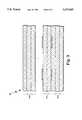
- FIG. 1is a cross-sectional view of a printed circuit board
- FIG. 2is a cross-sectional view of a flex printed circuit board having an inner layer
- FIG. 3is a cross-sectional view of a printed circuit board having a plurality of layers.
- FIG. 4is a cross-sectional view of a rigid-flex printed circuit board.
- a printed circuit board 10includes a conductive foil 12 having first and second opposing surfaces 12a, 12b.
- the conductive foil 12may be provided, for example, as a sheet of copper foil having a width of 25 or 38 inches. Those of skill in the art will recognize of course that any type conductive foil having any width may be used. The particular type, width and thickness of the foil 12 may be selected according to a number of factors including but not limited to the size and characteristics which results in efficient use of the foil, the width and thickness which results in the lowest manufacturing cost, etc.
- a first layer 14 of an adhesive resinis disposed on at least a first portion of foil surface 12b.
- This first resin layer 14is then cured using curing towers in a conventional curing process as is well known to those of ordinary skill in the art.
- a second layer 16 of the resinis applied over the cured resin layer 14.
- This second resin layer 16is then semi-cured using curing techniques well known to those of ordinary skill in the art.
- the combination of the conductive foil 12, cured adhesive 14 and semi-cured adhesive 16provide a coated conductive foil layer 17.
- the first and second resin layers 14, 16may be applied using standard coating techniques.
- the resinmay be applied to the foil through a coating head and then passed through a so-called drying tower.
- the drying towermay be provided as an infrared curing tower, a thermal air turbine tower, or any other type of drying apparatus well known to those of ordinary skill in the art.
- the first resin layermay be disposed having a thickness typically of about 0.001 inch and may be cured at a temperature typically of about 300 degrees Fahrenheit.
- the semi-cured resinmay be may be disposed having a thickness typically of about 0.00125 inches and may be cured at a temperature of about 200 degrees Fahrenheit. Other thicknesses and temperatures may of course be used.
- the resin layersmay be provided having thicknesses typically in the range of about 0.0005 inch to 0.003 inch and the resins may be cured at temperatures typically in the range of about 100 degrees Fahrenheit to 450 degrees Fahrenheit.
- the particular combination of resin thicknesses, curing times and curing temperaturesmay be selected according to a variety of factors including but not limited to the particular drying apparatus used, the particular type of resin used and the particular application. Those of ordinary skill in the art will know how to select the particular curing times and temperatures required to provide the first and second resin layers.
- the coated conductive foil layer 17is then disposed over a first surface 18a of a second substrate 18.
- the first surface of the second substrate 18has a plurality of conductors 20 disposed thereon.
- the conductors 20may be etched on the substrate 18, for example, to provide signal paths.
- the semi-cured resin layer 16is laminated on the inner layer 18.
- coated conductive foil layer 17may also be applied to the second surface 18b of the substrate 18 to thus create a sandwich.
- Such a processmay be accomplished using conventional equipment.
- bondingmay be done by simultaneously feeding the two coated conductive layers 17, 17' between two stainless steel plates and then processing the printed circuit 10 board in a conventional lamination press.
- this inventionmay be practiced using conventional lamination apparatus.
- the adhesive layers 14, 16may be provided as an epoxy type material. More particularly a tetrafunctional epoxy resin system may preferably be used. For example an epoxy identified as part number FR406 manufactured by Norplex Oak, Inc. Wisconsin may be used. Those of ordinary skill in the art will recognize of course that other resin systems may also be used. For example, dyfunctional, tetrafunctional, bismaleimide/triazine (BT), cyanide esser, or polyimide resin systems may be used.
- BTbismaleimide/triazine
- cyanide essercyanide esser
- polyimide resin systemsmay be used.
- each of the layersare bonded together to provide a single piece of material.
- the number of individual pieces which must be handledis minimized.
- the printer circuit board 10may correspond to a flexible or a rigid-flex pcb.
- a printed circuit board 26includes a substrate 28 having conductive foil regions 30a-30d, generally denoted 30, disposed over first and second surfaces thereof. Such conductors 30 need only be disposed where required.
- the substrate 28may be provided having surfaces which are free of conductive plating. That is, the substrate 28 may be provided having unplated surfaces or alternatively one or both inner layer surfaces may have a conductive plating disposed thereon.
- the substrate 28is disposed between a pair of coated conductive foil layers 32, which may be similar to the coated conductive foil layer 17 described above in conjunction with FIG. 1.
- Each of the conductive foil layers 32includes a conductive foil 34, a cured adhesive layer 36 and a semicured adhesive layer 38.
- the printed circuit board 26may be used in a mass lamination process.
- the substrates 28, 32are here disposed to provide the printed circuit board 26 as a six layer printed circuit board 26 having a first outer layer 26a, a first inner layer 26b, a second inner layer 26c a third inner layer 26d, a fourth inner layer 26e and a second outer layer 26f.
- the inner layers 26c, 26dare here provided having the conductors 30a-30d disposed thereon.
- a conductorsmay be provided, for example, as copper foil having a thickness typically in the range of about 0.0007 inches to 0.0042 inches.
- the printed circuit board 26corresponds to a so-called Type 3 printed circuit board as defined in MIL-P-50884.
- the coated conductive foil layers 32each include a conductive foil 34 which may be provided, for example, from a coated roll of electrodeposited or rolled annealed copper or other conductive metal.
- the conductive foil 34is provided having an adhesive 36 coated on a first surface thereof.
- the adhesive 36is cured and then a second adhesive 38 is disposed over the cured adhesive 36.
- the second adhesive 36is then semi-cured.
- the first and second adhesives 36, 38operate as a combined adhesive and dielectric material.
- each of the coated conductive foil layers 32includes conductive foil having a combined adhesive and dielectric disposed thereon.
- the coated conductive foil layers 32may then be simultaneously applied to the first and second opposing surfaces of the substrate 28.
- the combined adhesive and dielectric materialcontrols the dielectric thickness between the conductive foils and also controls the surface topography.
- the surface topography of the printed circuit board 26is suitable for machine processes and other post bonding processes.
- the printed circuit board 26is thus provided as a homogenous epoxy or polyimide adhesive system that maintains its modules of flexibility after curing. Also by separately curing the first and second adhesive coatings 36, 38 the dielectric distance between layers may be controlled. By providing the adhesive layers 36, 38 from a homogenous dielectric and bonding resin, the printed circuit board 26 is provided having a homogeneous dielectric constant and coefficient of thermal expansion. Furthermore, by providing the second adhesive layer 38 with a high flow resin displacement characteristic, the areas around conductors 30 disposed on the inner layers 26c, 26d may be effectively filled.
- the printed circuit board 26may be provided having a smooth surface.
- a plurality of such boardsmay be stacked and simultaneously drilled or processed through other machining processes.
- a printed circuit board 40includes a plurality of substrates 42a-42N, generally denoted 42.
- the substrates 42are here disposed to provide the printed circuit board 40.
- Each of the substrates 42correspond to coated conducted foil layers which may be provided using the same techniques as the coated conductive foil layers 17 and 32 described above in conjunction with FIGS. 1 and 2.
- each of the N substrates 42may be simultaneously bonded together using conventional techniques to provided the printed circuit board 40. Since the circuit 40 will be provided having even surface topographies, all machining steps such as drilling and the like may be simultaneously performed on the flat stack of N bonded substrates.
- a so-called Type 4 rigid-flex printed circuit board 50includes a flex portion 50a and a rigid portion 50b.
- the characteristics of a Type 4 printed circuit boardsare well known to those of skill in the art and are set forth in MIL-P50884.
- the printed circuit board 50includes an inner layer 52 having first and second opposing surfaces 52a, 52b.
- the surface 52ahas a conductive plating 54 disposed thereon.
- the layer 52may or may not have a conductive plating disposed thereon. That is, the layer 52 may be provided having unplated surfaces or alternatively one or both inner layer surfaces 52a, 52b may have a conductive plating disposed thereon.
- the inner layer 52is disposed between a pair of coated conductive foil layers 56.
- the printed circuit boardmay be used in a mass lamination process.
- the coated conductive foil layers 56may each be provided in a manner similar to the coated conductive foil layers 17, 32 and 42 described in conjunction with FIGS. 1-3 above.
- the printed circuit board 50is thus provided as a homogenous epoxy or polyimide adhesive system that maintains its modules of flexibility after curing and is provided having an even surface topography.
- a rigid-flex printed circuit board having three or more layersmay be provided having an even surface topography.
- the multiple layer rigid-flex printed circuit board 50may be provided having a homogeneous construction and without the use of any woven materials. That is, with the present invention no glass or any other woven materials are used in the rigid-flex printed circuit board. Thus, both the inner and outer layers of the rigid-flex printed circuit board 50 are provided from non-woven materials.
- the multi-layer rigid-flex printed circuit board having a homogeneous constructionis provided from non-woven inner layers and non-woven bonding materials such as straight epoxy.
- a multi-layer rigid-flex printed circuit boardis provided without the use of pre-impregnated glass cloth or other woven materials.
- the Type 4 rigid-flex printed circuit board 50may thus be provided from a combination of resins and materials which eliminate the use of woven materials such as glass fabric as coating mediums as well as an insulators. This allows each of the layers of the printed circuit board 50 to thermally dissipate heat in any linear radial direction about the thermal source.
- the thermal pathsare substantially confined to paths which lie in the traditional machine and transverse directions of the woven material, as is known for example, with 104 to 7628 glass fabric that has been coated into so-called prepreg material.
- non-woven highly thermally stabile materialssuch as aramid thin core inner layers coated with the same resin system may be used to provide a printed circuit board having homogenous nonwoven layers.
- the printed circuit board 50 of the present inventionis therefore provided having a thermal stability which is more uniform than heretofore and consequently such printed circuit boards suffer a reduced number of defects due to measeling for example. Moreover, by eliminating the glass and other woven fabric, the printed circuit board 50 may be provided as a relatively thin printed circuit board.
Landscapes
- Engineering & Computer Science (AREA)
- Manufacturing & Machinery (AREA)
- Microelectronics & Electronic Packaging (AREA)
- Production Of Multi-Layered Print Wiring Board (AREA)
- Combinations Of Printed Boards (AREA)
- Manufacturing Of Printed Wiring (AREA)
- Structure Of Printed Boards (AREA)
Abstract
Description
Claims (6)
Priority Applications (1)
| Application Number | Priority Date | Filing Date | Title |
|---|---|---|---|
| US08/297,792US5557843A (en) | 1993-08-23 | 1994-08-30 | Method of making a circuit board or layer thereof including semi-curing a second adhesive coated on a cured first adhesive |
Applications Claiming Priority (2)
| Application Number | Priority Date | Filing Date | Title |
|---|---|---|---|
| US08/110,437US5362534A (en) | 1993-08-23 | 1993-08-23 | Multiple layer printed circuit boards and method of manufacture |
| US08/297,792US5557843A (en) | 1993-08-23 | 1994-08-30 | Method of making a circuit board or layer thereof including semi-curing a second adhesive coated on a cured first adhesive |
Related Parent Applications (1)
| Application Number | Title | Priority Date | Filing Date |
|---|---|---|---|
| US08/110,437DivisionUS5362534A (en) | 1993-08-23 | 1993-08-23 | Multiple layer printed circuit boards and method of manufacture |
Publications (1)
| Publication Number | Publication Date |
|---|---|
| US5557843Atrue US5557843A (en) | 1996-09-24 |
Family
ID=22333005
Family Applications (2)
| Application Number | Title | Priority Date | Filing Date |
|---|---|---|---|
| US08/110,437Expired - LifetimeUS5362534A (en) | 1993-08-23 | 1993-08-23 | Multiple layer printed circuit boards and method of manufacture |
| US08/297,792Expired - LifetimeUS5557843A (en) | 1993-08-23 | 1994-08-30 | Method of making a circuit board or layer thereof including semi-curing a second adhesive coated on a cured first adhesive |
Family Applications Before (1)
| Application Number | Title | Priority Date | Filing Date |
|---|---|---|---|
| US08/110,437Expired - LifetimeUS5362534A (en) | 1993-08-23 | 1993-08-23 | Multiple layer printed circuit boards and method of manufacture |
Country Status (8)
| Country | Link |
|---|---|
| US (2) | US5362534A (en) |
| EP (1) | EP0715570B1 (en) |
| JP (1) | JPH09501800A (en) |
| KR (1) | KR100195528B1 (en) |
| CN (1) | CN1046078C (en) |
| CA (1) | CA2169547C (en) |
| DE (1) | DE69431723T2 (en) |
| WO (1) | WO1995005938A1 (en) |
Cited By (19)
| Publication number | Priority date | Publication date | Assignee | Title |
|---|---|---|---|---|
| US5793150A (en)* | 1994-07-07 | 1998-08-11 | Firma Carl Freudenberg | Flat seal |
| US5873162A (en)* | 1997-02-11 | 1999-02-23 | International Business Machines Corporation | Technique for attaching a stiffener to a flexible substrate |
| WO2000009327A1 (en)* | 1998-08-11 | 2000-02-24 | Ga-Tek Inc. (D.B.A. Gould Electronics Inc.) | Resin/copper/metal laminate and method of producing same |
| GB2344299A (en)* | 1998-12-03 | 2000-06-07 | Rexam Custom Limited | Method of producing adhesive coated foil |
| US6317023B1 (en)* | 1999-10-15 | 2001-11-13 | E. I. Du Pont De Nemours And Company | Method to embed passive components |
| WO2001049797A3 (en)* | 1999-03-31 | 2001-12-20 | Minnesota Mining & Mfg | Multi-layered sealant |
| US6518516B2 (en) | 2000-04-25 | 2003-02-11 | International Business Machines Corporation | Multilayered laminate |
| US6596391B2 (en) | 1997-05-14 | 2003-07-22 | Honeywell International Inc. | Very ultra thin conductor layers for printed wiring boards |
| US20040040152A1 (en)* | 2002-08-30 | 2004-03-04 | Hiroyuki Kigami | Manufacturing method of liquid jet recording head |
| US6740399B1 (en) | 1999-03-31 | 2004-05-25 | 3M Innovative Properties Company | Multi-layered sealant |
| US20040099999A1 (en)* | 2002-10-11 | 2004-05-27 | Borland William J. | Co-fired capacitor and method for forming ceramic capacitors for use in printed wiring boards |
| US6768052B2 (en)* | 2002-02-08 | 2004-07-27 | Mitsumi Electric Co., Ltd. | Flexible printed circuit with EMI protection |
| US6832436B2 (en) | 2000-04-25 | 2004-12-21 | International Business Machines Corporation | Method for forming a substructure of a multilayered laminate |
| US6906120B1 (en) | 2000-06-20 | 2005-06-14 | General Electric | Poly(arylene ether) adhesive compositions |
| US20050195554A1 (en)* | 2002-10-11 | 2005-09-08 | Borland William J. | High tolerance embedded capacitors |
| US20060120015A1 (en)* | 2004-12-02 | 2006-06-08 | Borland William J | Thick-film capacitors, embedding thick-film capacitors inside printed circuit boards, and methods of forming such capacitors and printed circuit boards |
| US20060141225A1 (en)* | 2004-12-28 | 2006-06-29 | Borland William J | Oxygen doped firing of barium titanate on copper foil |
| US20100175914A1 (en)* | 2009-01-12 | 2010-07-15 | Oak-Mitsui Technologies Llc | Passive electrical devices and methods of fabricating passive electrical devices |
| US20130141405A1 (en)* | 2011-08-05 | 2013-06-06 | Polymer Vision B.V. | Electrofluidic chromatophore (efc) display apparatus |
Families Citing this family (14)
| Publication number | Priority date | Publication date | Assignee | Title |
|---|---|---|---|---|
| US5739476A (en)* | 1994-10-05 | 1998-04-14 | Namgung; Chung | Multilayer printed circuit board laminated with unreinforced resin |
| JP3676375B2 (en)* | 1995-07-04 | 2005-07-27 | 三井金属鉱業株式会社 | Copper foil with resin for multilayer printed wiring board and multilayer printed wiring board using the copper foil |
| WO1997018695A1 (en)* | 1995-11-15 | 1997-05-22 | Dyconex Patente Ag | Process for making multi-layer foil printed circuit boards |
| AU2105300A (en)* | 1999-01-14 | 2000-08-01 | Hans-Jurgen Schafer | Method and device for producing copper foil which is coated with polymers on both sides and which is laminated onto printed circuit boards |
| CN1081128C (en)* | 1999-08-18 | 2002-03-20 | 湖北省化学研究所 | Manufacture of metal sheet coated with polymer film specially for soft printed circuit |
| TW479442B (en)* | 1999-10-20 | 2002-03-11 | Samsung Electro Mech | Printed circuit board for RAMBUS |
| US6284982B1 (en)* | 2000-08-18 | 2001-09-04 | Ga-Tek Inc. | Method and component for forming an embedded resistor in a multi-layer printed circuit |
| US6656314B2 (en)* | 2001-05-23 | 2003-12-02 | Hewlett-Packard Development Company, L.P. | Method of manufacturing multilayer substrates |
| DE102004014300A1 (en)* | 2004-03-22 | 2005-10-06 | Endress + Hauser Flowtec Ag, Reinach | Device for measuring and / or monitoring the flow of a measuring medium |
| US9975625B2 (en) | 2010-04-19 | 2018-05-22 | The Boeing Company | Laminated plasma actuator |
| CN103299393B (en)* | 2010-10-19 | 2017-02-15 | 惠亚集团公司 | Method of manufacturing printed circuit boards having vias with wrap plating |
| CN102886946B (en)* | 2011-05-10 | 2015-04-15 | 深圳光启高等理工研究院 | Heterogeneous material and preparation method thereof |
| CN104349610B (en)* | 2013-07-24 | 2018-03-27 | 北大方正集团有限公司 | The manufacture method and printed circuit board of printed circuit board daughter board and printed circuit board |
| EP3318113A1 (en)* | 2015-06-30 | 2018-05-09 | 3M Innovative Properties Company | Electronic devices comprising a via and methods of forming such electronic devices |
Citations (50)
| Publication number | Priority date | Publication date | Assignee | Title |
|---|---|---|---|---|
| US2923651A (en)* | 1954-12-15 | 1960-02-02 | John V Petriello | Metal-plastic film laminates |
| US3795047A (en)* | 1972-06-15 | 1974-03-05 | Ibm | Electrical interconnect structuring for laminate assemblies and fabricating methods therefor |
| US3936575A (en)* | 1973-02-21 | 1976-02-03 | Sumitomo Bakelite Company, Limited | Flexible metal-clad laminates and method for manufacturing the same |
| US3962520A (en)* | 1973-06-20 | 1976-06-08 | Sumitomo Bakelite Company, Limited | Adhesive composition for flexible printed circuit and method for using the same |
| US4215387A (en)* | 1977-10-06 | 1980-07-29 | Asahi Kogaku Kogyo Kabushiki Kaisha | Multi-layer flexible printed circuit board assembly |
| US4311749A (en)* | 1977-09-06 | 1982-01-19 | Nippondenso Co., Ltd. | Flame-proof flexible printed circuit board |
| US4338149A (en)* | 1979-11-20 | 1982-07-06 | Kollmorgen Technologies Corporation | Process for making circuit boards having rigid and flexible areas |
| GB2111313A (en)* | 1981-12-11 | 1983-06-29 | Western Electric Co | Multi-layer circuit board fabrication |
| US4556628A (en)* | 1983-05-19 | 1985-12-03 | International Business Machines Corporation | Process for producing printed circuit boards with metallic conductor structures embedded in the insulating substrate |
| US4582564A (en)* | 1982-01-04 | 1986-04-15 | At&T Technologies, Inc. | Method of providing an adherent metal coating on an epoxy surface |
| US4671968A (en)* | 1985-04-01 | 1987-06-09 | Macdermid, Incorporated | Method for electroless deposition of copper on conductive surfaces and on substrates containing conductive surfaces |
| US4774122A (en)* | 1986-10-14 | 1988-09-27 | Edward Adler | Resinous product provided with surface coatable with metal layer bonded through an array of microdendrites and metal-clad resinous product thereof |
| US4775444A (en)* | 1987-08-26 | 1988-10-04 | Macdermid, Incorporated | Process for fabricating multilayer circuit boards |
| US4781969A (en)* | 1986-10-03 | 1988-11-01 | Junkosha Co., Ltd. | Flexible printed circuit board |
| US4783247A (en)* | 1985-05-17 | 1988-11-08 | Hoechst Aktiengesellschaft | Method and manufacture for electrically insulating base material used in plated-through printed circuit panels |
| JPS63305594A (en)* | 1987-06-05 | 1988-12-13 | Sumitomo Bakelite Co Ltd | Manufacture of multilayer printed circuit board |
| US4800461A (en)* | 1987-11-02 | 1989-01-24 | Teledyne Industries, Inc. | Multilayer combined rigid and flex printed circuits |
| US4897165A (en)* | 1988-08-23 | 1990-01-30 | Shipley Company Inc. | Electroplating composition and process for plating through holes in printed circuit boards |
| US4897118A (en)* | 1986-11-10 | 1990-01-30 | Macdermid, Incorporated | Selective metallization process, additive method for manufacturing printed circuit boards, and composition for use therein |
| US4915797A (en)* | 1989-05-24 | 1990-04-10 | Yates Industries, Inc. | Continuous process for coating printed circuit grade copper foil with a protective resin |
| US4932518A (en)* | 1988-08-23 | 1990-06-12 | Shipley Company Inc. | Method and apparatus for determining throwing power of an electroplating solution |
| US4958050A (en)* | 1988-05-13 | 1990-09-18 | Minolta Camera Kabushiki Kaisha | Flexible printed circuit board |
| US4964945A (en)* | 1988-12-09 | 1990-10-23 | Minnesota Mining And Manufacturing Company | Lift off patterning process on a flexible substrate |
| US4969979A (en)* | 1989-05-08 | 1990-11-13 | International Business Machines Corporation | Direct electroplating of through holes |
| US5004525A (en)* | 1988-08-23 | 1991-04-02 | Shipley Company Inc. | Copper electroplating composition |
| US5004639A (en)* | 1990-01-23 | 1991-04-02 | Sheldahl, Inc. | Rigid flex printed circuit configuration |
| US5068013A (en)* | 1988-08-23 | 1991-11-26 | Shipley Company Inc. | Electroplating composition and process |
| US5072074A (en)* | 1990-07-24 | 1991-12-10 | Interflex Corporation | High yield combined rigid and flexible printed circuits and method of manufacture |
| US5084124A (en)* | 1989-04-28 | 1992-01-28 | Nikkan Industries Co., Ltd. | Flexible printed circuit board and coverlay film and method of manufacturing same |
| US5097390A (en)* | 1986-12-10 | 1992-03-17 | Interflex Corporation | Printed circuit and fabrication of same |
| US5095628A (en)* | 1990-08-09 | 1992-03-17 | Teledyne Industries, Inc. | Process of forming a rigid-flex circuit |
| US5100492A (en)* | 1989-07-07 | 1992-03-31 | Firma Carl Freudenberg | Process for manufacturing printed-circuit boards having rigid and flexible areas |
| US5112694A (en)* | 1989-07-31 | 1992-05-12 | Chisso Corporation | Flexible printed-circuit base board and process for producing the same |
| US5121297A (en)* | 1990-12-31 | 1992-06-09 | Compaq Computer Corporation | Flexible printed circuits |
| US5129142A (en)* | 1990-10-30 | 1992-07-14 | International Business Machines Corporation | Encapsulated circuitized power core alignment and lamination |
| US5142448A (en)* | 1990-02-05 | 1992-08-25 | Horst Kober | Method for manufacturing rigid-flexible multilayer circuit boards and products thereof |
| US5144534A (en)* | 1990-02-05 | 1992-09-01 | Horst Kober | Method for manufacturing rigid-flexible circuit boards and products thereof |
| US5144742A (en)* | 1991-02-27 | 1992-09-08 | Zycon Corporation | Method of making rigid-flex printed circuit boards |
| US5147208A (en)* | 1991-06-28 | 1992-09-15 | Rogers Corporation | Flexible printed circuit with raised contacts |
| US5153987A (en)* | 1988-07-15 | 1992-10-13 | Hitachi Chemical Company, Ltd. | Process for producing printed wiring boards |
| US5162140A (en)* | 1989-04-28 | 1992-11-10 | Nikkan Industries Co., Ltd. | Flexible printed circuit board and coverlay film and manufacture methods therefor |
| US5172472A (en)* | 1991-08-15 | 1992-12-22 | Direct Imaging Inc. | Multi-layer rigid prototype printed circuit board fabrication method |
| US5173150A (en)* | 1990-04-23 | 1992-12-22 | Mitsubishi Gas Chemical Co., Ltd. | Process for producing printed circuit board |
| US5175047A (en)* | 1990-08-09 | 1992-12-29 | Teledyne Industries, Inc. | Rigid-flex printed circuit |
| US5178318A (en)* | 1990-10-12 | 1993-01-12 | Compaq Computer Corp. | Multilayer rigid-flex printed circuit boards for use in infrared reflow oven and method for assembling same |
| US5206463A (en)* | 1990-07-24 | 1993-04-27 | Miraco, Inc. | Combined rigid and flexible printed circuits and method of manufacture |
| US5214571A (en)* | 1986-12-10 | 1993-05-25 | Miraco, Inc. | Multilayer printed circuit and associated multilayer material |
| US5213840A (en)* | 1990-05-01 | 1993-05-25 | Macdermid, Incorporated | Method for improving adhesion to polymide surfaces |
| JPH05218616A (en)* | 1992-02-05 | 1993-08-27 | Cmk Corp | Manufacture of flexible printed wiring board |
| US5344893A (en)* | 1991-07-23 | 1994-09-06 | Ibiden Co., Ltd. | Epoxy/amino powder resin adhesive for printed circuit board |
Family Cites Families (7)
| Publication number | Priority date | Publication date | Assignee | Title |
|---|---|---|---|---|
| GB1145771A (en)* | 1965-03-18 | 1969-03-19 | Litton Industries Inc | Electrical circuit boards |
| JPH0719972B2 (en)* | 1986-08-29 | 1995-03-06 | 富士通株式会社 | Copper foil with resin for multilayer printed boards |
| JP2631287B2 (en)* | 1987-06-30 | 1997-07-16 | 日本メクトロン 株式会社 | Manufacturing method of hybrid multilayer circuit board |
| JP2817947B2 (en)* | 1989-05-11 | 1998-10-30 | ジャパンゴアテックス株式会社 | Adhesive sheet for multilayer printed circuit board |
| JPH03187293A (en)* | 1989-12-15 | 1991-08-15 | Hitachi Chem Co Ltd | Manufacture of copper-clad laminate |
| JPH04278598A (en)* | 1991-03-07 | 1992-10-05 | Nec Corp | Manufacture of multilayer printed circuit board |
| JPH05206649A (en)* | 1991-05-07 | 1993-08-13 | Matsushita Electric Works Ltd | Multilayer printed wiring board |
- 1993
- 1993-08-23USUS08/110,437patent/US5362534A/ennot_activeExpired - Lifetime
- 1994
- 1994-08-23JPJP50772295Apatent/JPH09501800A/enactivePending
- 1994-08-23EPEP94925993Apatent/EP0715570B1/ennot_activeExpired - Lifetime
- 1994-08-23CACA 2169547patent/CA2169547C/ennot_activeExpired - Lifetime
- 1994-08-23KRKR1019960700894Apatent/KR100195528B1/ennot_activeExpired - Lifetime
- 1994-08-23CNCN94193145Apatent/CN1046078C/ennot_activeExpired - Lifetime
- 1994-08-23DEDE69431723Tpatent/DE69431723T2/ennot_activeExpired - Lifetime
- 1994-08-23WOPCT/US1994/009495patent/WO1995005938A1/enactiveIP Right Grant
- 1994-08-30USUS08/297,792patent/US5557843A/ennot_activeExpired - Lifetime
Patent Citations (50)
| Publication number | Priority date | Publication date | Assignee | Title |
|---|---|---|---|---|
| US2923651A (en)* | 1954-12-15 | 1960-02-02 | John V Petriello | Metal-plastic film laminates |
| US3795047A (en)* | 1972-06-15 | 1974-03-05 | Ibm | Electrical interconnect structuring for laminate assemblies and fabricating methods therefor |
| US3936575A (en)* | 1973-02-21 | 1976-02-03 | Sumitomo Bakelite Company, Limited | Flexible metal-clad laminates and method for manufacturing the same |
| US3962520A (en)* | 1973-06-20 | 1976-06-08 | Sumitomo Bakelite Company, Limited | Adhesive composition for flexible printed circuit and method for using the same |
| US4311749A (en)* | 1977-09-06 | 1982-01-19 | Nippondenso Co., Ltd. | Flame-proof flexible printed circuit board |
| US4215387A (en)* | 1977-10-06 | 1980-07-29 | Asahi Kogaku Kogyo Kabushiki Kaisha | Multi-layer flexible printed circuit board assembly |
| US4338149A (en)* | 1979-11-20 | 1982-07-06 | Kollmorgen Technologies Corporation | Process for making circuit boards having rigid and flexible areas |
| GB2111313A (en)* | 1981-12-11 | 1983-06-29 | Western Electric Co | Multi-layer circuit board fabrication |
| US4582564A (en)* | 1982-01-04 | 1986-04-15 | At&T Technologies, Inc. | Method of providing an adherent metal coating on an epoxy surface |
| US4556628A (en)* | 1983-05-19 | 1985-12-03 | International Business Machines Corporation | Process for producing printed circuit boards with metallic conductor structures embedded in the insulating substrate |
| US4671968A (en)* | 1985-04-01 | 1987-06-09 | Macdermid, Incorporated | Method for electroless deposition of copper on conductive surfaces and on substrates containing conductive surfaces |
| US4783247A (en)* | 1985-05-17 | 1988-11-08 | Hoechst Aktiengesellschaft | Method and manufacture for electrically insulating base material used in plated-through printed circuit panels |
| US4781969A (en)* | 1986-10-03 | 1988-11-01 | Junkosha Co., Ltd. | Flexible printed circuit board |
| US4774122A (en)* | 1986-10-14 | 1988-09-27 | Edward Adler | Resinous product provided with surface coatable with metal layer bonded through an array of microdendrites and metal-clad resinous product thereof |
| US4897118A (en)* | 1986-11-10 | 1990-01-30 | Macdermid, Incorporated | Selective metallization process, additive method for manufacturing printed circuit boards, and composition for use therein |
| US5097390A (en)* | 1986-12-10 | 1992-03-17 | Interflex Corporation | Printed circuit and fabrication of same |
| US5214571A (en)* | 1986-12-10 | 1993-05-25 | Miraco, Inc. | Multilayer printed circuit and associated multilayer material |
| JPS63305594A (en)* | 1987-06-05 | 1988-12-13 | Sumitomo Bakelite Co Ltd | Manufacture of multilayer printed circuit board |
| US4775444A (en)* | 1987-08-26 | 1988-10-04 | Macdermid, Incorporated | Process for fabricating multilayer circuit boards |
| US4800461A (en)* | 1987-11-02 | 1989-01-24 | Teledyne Industries, Inc. | Multilayer combined rigid and flex printed circuits |
| US4958050A (en)* | 1988-05-13 | 1990-09-18 | Minolta Camera Kabushiki Kaisha | Flexible printed circuit board |
| US5153987A (en)* | 1988-07-15 | 1992-10-13 | Hitachi Chemical Company, Ltd. | Process for producing printed wiring boards |
| US4932518A (en)* | 1988-08-23 | 1990-06-12 | Shipley Company Inc. | Method and apparatus for determining throwing power of an electroplating solution |
| US5004525A (en)* | 1988-08-23 | 1991-04-02 | Shipley Company Inc. | Copper electroplating composition |
| US5068013A (en)* | 1988-08-23 | 1991-11-26 | Shipley Company Inc. | Electroplating composition and process |
| US4897165A (en)* | 1988-08-23 | 1990-01-30 | Shipley Company Inc. | Electroplating composition and process for plating through holes in printed circuit boards |
| US4964945A (en)* | 1988-12-09 | 1990-10-23 | Minnesota Mining And Manufacturing Company | Lift off patterning process on a flexible substrate |
| US5162140A (en)* | 1989-04-28 | 1992-11-10 | Nikkan Industries Co., Ltd. | Flexible printed circuit board and coverlay film and manufacture methods therefor |
| US5084124A (en)* | 1989-04-28 | 1992-01-28 | Nikkan Industries Co., Ltd. | Flexible printed circuit board and coverlay film and method of manufacturing same |
| US4969979A (en)* | 1989-05-08 | 1990-11-13 | International Business Machines Corporation | Direct electroplating of through holes |
| US4915797A (en)* | 1989-05-24 | 1990-04-10 | Yates Industries, Inc. | Continuous process for coating printed circuit grade copper foil with a protective resin |
| US5100492A (en)* | 1989-07-07 | 1992-03-31 | Firma Carl Freudenberg | Process for manufacturing printed-circuit boards having rigid and flexible areas |
| US5112694A (en)* | 1989-07-31 | 1992-05-12 | Chisso Corporation | Flexible printed-circuit base board and process for producing the same |
| US5004639A (en)* | 1990-01-23 | 1991-04-02 | Sheldahl, Inc. | Rigid flex printed circuit configuration |
| US5142448A (en)* | 1990-02-05 | 1992-08-25 | Horst Kober | Method for manufacturing rigid-flexible multilayer circuit boards and products thereof |
| US5144534A (en)* | 1990-02-05 | 1992-09-01 | Horst Kober | Method for manufacturing rigid-flexible circuit boards and products thereof |
| US5173150A (en)* | 1990-04-23 | 1992-12-22 | Mitsubishi Gas Chemical Co., Ltd. | Process for producing printed circuit board |
| US5213840A (en)* | 1990-05-01 | 1993-05-25 | Macdermid, Incorporated | Method for improving adhesion to polymide surfaces |
| US5072074A (en)* | 1990-07-24 | 1991-12-10 | Interflex Corporation | High yield combined rigid and flexible printed circuits and method of manufacture |
| US5206463A (en)* | 1990-07-24 | 1993-04-27 | Miraco, Inc. | Combined rigid and flexible printed circuits and method of manufacture |
| US5095628A (en)* | 1990-08-09 | 1992-03-17 | Teledyne Industries, Inc. | Process of forming a rigid-flex circuit |
| US5175047A (en)* | 1990-08-09 | 1992-12-29 | Teledyne Industries, Inc. | Rigid-flex printed circuit |
| US5178318A (en)* | 1990-10-12 | 1993-01-12 | Compaq Computer Corp. | Multilayer rigid-flex printed circuit boards for use in infrared reflow oven and method for assembling same |
| US5129142A (en)* | 1990-10-30 | 1992-07-14 | International Business Machines Corporation | Encapsulated circuitized power core alignment and lamination |
| US5121297A (en)* | 1990-12-31 | 1992-06-09 | Compaq Computer Corporation | Flexible printed circuits |
| US5144742A (en)* | 1991-02-27 | 1992-09-08 | Zycon Corporation | Method of making rigid-flex printed circuit boards |
| US5147208A (en)* | 1991-06-28 | 1992-09-15 | Rogers Corporation | Flexible printed circuit with raised contacts |
| US5344893A (en)* | 1991-07-23 | 1994-09-06 | Ibiden Co., Ltd. | Epoxy/amino powder resin adhesive for printed circuit board |
| US5172472A (en)* | 1991-08-15 | 1992-12-22 | Direct Imaging Inc. | Multi-layer rigid prototype printed circuit board fabrication method |
| JPH05218616A (en)* | 1992-02-05 | 1993-08-27 | Cmk Corp | Manufacture of flexible printed wiring board |
Cited By (31)
| Publication number | Priority date | Publication date | Assignee | Title |
|---|---|---|---|---|
| US5793150A (en)* | 1994-07-07 | 1998-08-11 | Firma Carl Freudenberg | Flat seal |
| US5873162A (en)* | 1997-02-11 | 1999-02-23 | International Business Machines Corporation | Technique for attaching a stiffener to a flexible substrate |
| US6596391B2 (en) | 1997-05-14 | 2003-07-22 | Honeywell International Inc. | Very ultra thin conductor layers for printed wiring boards |
| US6770380B2 (en) | 1998-08-11 | 2004-08-03 | Nikko Materials Usa, Inc. | Resin/copper/metal laminate and method of producing same |
| US6376008B1 (en) | 1998-08-11 | 2002-04-23 | Gould Electronics Inc. | Resin/copper/metal laminate and method of producing same |
| WO2000009327A1 (en)* | 1998-08-11 | 2000-02-24 | Ga-Tek Inc. (D.B.A. Gould Electronics Inc.) | Resin/copper/metal laminate and method of producing same |
| WO2000033627A1 (en)* | 1998-12-03 | 2000-06-08 | Rexam Cfp Limited | Method for producing adhesive coated foil |
| GB2344299A (en)* | 1998-12-03 | 2000-06-07 | Rexam Custom Limited | Method of producing adhesive coated foil |
| WO2001049797A3 (en)* | 1999-03-31 | 2001-12-20 | Minnesota Mining & Mfg | Multi-layered sealant |
| US6740399B1 (en) | 1999-03-31 | 2004-05-25 | 3M Innovative Properties Company | Multi-layered sealant |
| US6317023B1 (en)* | 1999-10-15 | 2001-11-13 | E. I. Du Pont De Nemours And Company | Method to embed passive components |
| US6518516B2 (en) | 2000-04-25 | 2003-02-11 | International Business Machines Corporation | Multilayered laminate |
| US6832436B2 (en) | 2000-04-25 | 2004-12-21 | International Business Machines Corporation | Method for forming a substructure of a multilayered laminate |
| US6906120B1 (en) | 2000-06-20 | 2005-06-14 | General Electric | Poly(arylene ether) adhesive compositions |
| US7090920B2 (en) | 2000-06-20 | 2006-08-15 | General Electric Company | Poly(arylene ether) adhesive compositions |
| US20050158552A1 (en)* | 2000-06-20 | 2005-07-21 | Davis Michael J. | Poly(arylene ether) adhesive compositions |
| US6768052B2 (en)* | 2002-02-08 | 2004-07-27 | Mitsumi Electric Co., Ltd. | Flexible printed circuit with EMI protection |
| US20040040152A1 (en)* | 2002-08-30 | 2004-03-04 | Hiroyuki Kigami | Manufacturing method of liquid jet recording head |
| US7171748B2 (en)* | 2002-08-30 | 2007-02-06 | Canon Kabushiki Kaisha | Method of manufacturing a liquid jet recording head |
| US20040099999A1 (en)* | 2002-10-11 | 2004-05-27 | Borland William J. | Co-fired capacitor and method for forming ceramic capacitors for use in printed wiring boards |
| US20040233611A1 (en)* | 2002-10-11 | 2004-11-25 | Borland William J. | Co-fired ceramic capacitor and method for forming ceramic capacitors for use in printed wiring boards |
| US20050195554A1 (en)* | 2002-10-11 | 2005-09-08 | Borland William J. | High tolerance embedded capacitors |
| EP1408520A3 (en)* | 2002-10-11 | 2005-02-09 | E.I. Du Pont De Nemours And Company | Co-fired ceramic capacitor and method for forming ceramic capacitors for use in printed wiring boards |
| US7072167B2 (en) | 2002-10-11 | 2006-07-04 | E. I. Du Pont De Nemours And Company | Co-fired ceramic capacitor and method for forming ceramic capacitors for use in printed wiring boards |
| US20060120015A1 (en)* | 2004-12-02 | 2006-06-08 | Borland William J | Thick-film capacitors, embedding thick-film capacitors inside printed circuit boards, and methods of forming such capacitors and printed circuit boards |
| US20070220725A1 (en)* | 2004-12-02 | 2007-09-27 | E.I. Du Pont De Nemours And Company | Thick-film capacitors, embedding thick-film capacitors inside printed circuit boards, and methods of forming such capacitors and printed circuit boards |
| US20060141225A1 (en)* | 2004-12-28 | 2006-06-29 | Borland William J | Oxygen doped firing of barium titanate on copper foil |
| US20100175914A1 (en)* | 2009-01-12 | 2010-07-15 | Oak-Mitsui Technologies Llc | Passive electrical devices and methods of fabricating passive electrical devices |
| US8866018B2 (en) | 2009-01-12 | 2014-10-21 | Oak-Mitsui Technologies Llc | Passive electrical devices and methods of fabricating passive electrical devices |
| US20130141405A1 (en)* | 2011-08-05 | 2013-06-06 | Polymer Vision B.V. | Electrofluidic chromatophore (efc) display apparatus |
| US9070322B2 (en)* | 2011-08-05 | 2015-06-30 | Creator Technology B.V. | Electrofluidic chromatophore (EFC) display apparatus |
Also Published As
| Publication number | Publication date |
|---|---|
| JPH09501800A (en) | 1997-02-18 |
| DE69431723D1 (en) | 2002-12-19 |
| EP0715570A1 (en) | 1996-06-12 |
| EP0715570B1 (en) | 2002-11-13 |
| CN1129423A (en) | 1996-08-21 |
| WO1995005938A1 (en) | 1995-03-02 |
| EP0715570A4 (en) | 1998-01-14 |
| US5362534A (en) | 1994-11-08 |
| KR100195528B1 (en) | 1999-06-15 |
| CA2169547C (en) | 2001-01-02 |
| CN1046078C (en) | 1999-10-27 |
| CA2169547A1 (en) | 1995-03-02 |
| KR960703722A (en) | 1996-08-31 |
| DE69431723T2 (en) | 2003-09-18 |
Similar Documents
| Publication | Publication Date | Title |
|---|---|---|
| US5557843A (en) | Method of making a circuit board or layer thereof including semi-curing a second adhesive coated on a cured first adhesive | |
| US5800650A (en) | Flexible multilayer printed circuit boards and methods of manufacture | |
| US6180215B1 (en) | Multilayer printed circuit board and manufacturing method thereof | |
| US6268070B1 (en) | Laminate for multi-layer printed circuit | |
| US4407883A (en) | Laminates for printed circuit boards | |
| US4985294A (en) | Printed wiring board | |
| JP3944921B2 (en) | Manufacturing method of multilayer wiring board | |
| US6713682B1 (en) | Through hole conduction structure of flexible multilayer circuit board and forming method thereof | |
| JPH07176837A (en) | Rigid flex printed wiring board and manufacturing method thereof | |
| JPH0199288A (en) | Manufacture of multi-layer printed wiring board | |
| WO1999057949A1 (en) | Intermediate layer to improve peel strength of copper foils | |
| JPS6223198A (en) | Making of multilayer interconnection board | |
| JPS59232846A (en) | Laminated board for electric wiring board and manufacture thereof | |
| JPS63199636A (en) | Laminated board | |
| JPH0750455A (en) | Rigid flex printed wiring board and manufacturing method thereof | |
| JPH0685406A (en) | Rigid flexible printed wirig board | |
| JPS63224936A (en) | Laminated board | |
| JPH06338663A (en) | Rigid flex printed wiring board and manufacturing method thereof | |
| KR100332973B1 (en) | Printed circuit board for impedance control | |
| JP2000286560A (en) | Multilayer fluororesin substrate and method of manufacturing the same | |
| JPH07142831A (en) | Copper-clad laminated board | |
| JPH0846362A (en) | Printed wiring board | |
| JP2003094571A (en) | Material for producing printed wiring board and its production method | |
| JPS63199245A (en) | Laminated board | |
| JPH0374895A (en) | Multilayer copper coated laminated board |
Legal Events
| Date | Code | Title | Description |
|---|---|---|---|
| STCF | Information on status: patent grant | Free format text:PATENTED CASE | |
| FEPP | Fee payment procedure | Free format text:PAT HLDR NO LONGER CLAIMS SMALL ENT STAT AS INDIV INVENTOR (ORIGINAL EVENT CODE: LSM1); ENTITY STATUS OF PATENT OWNER: LARGE ENTITY | |
| AS | Assignment | Owner name:PARLEX CORPORATION, MASSACHUSETTS Free format text:ASSIGNMENT OF SECURITY INTEREST;ASSIGNOR:POLYCLAD LAMINATES, INC.;REEL/FRAME:010602/0807 Effective date:20000106 | |
| FPAY | Fee payment | Year of fee payment:4 | |
| AS | Assignment | Owner name:POLYCLAD LAMINATES, INC., NEW HAMPSHIRE Free format text:ASSIGNMENT AGREEMENT;ASSIGNOR:PARLEX CORPORATION;REEL/FRAME:011035/0966 Effective date:20000106 | |
| AS | Assignment | Owner name:POLYCLAD LAMINATES, INC., NEW HAMPSHIRE Free format text:RELEASE OF SECURITY INTEREST IN PATENTS;ASSIGNOR:PARLEX CORPORATION;REEL/FRAME:014108/0452 Effective date:20030505 | |
| FPAY | Fee payment | Year of fee payment:8 | |
| AS | Assignment | Owner name:OBSIDIAN, LLC,CALIFORNIA Free format text:SECURITY AGREEMENT;ASSIGNOR:POLYCLAD LAMINATES, INC.;REEL/FRAME:018039/0781 Effective date:20060421 Owner name:OBSIDIAN, LLC, CALIFORNIA Free format text:SECURITY AGREEMENT;ASSIGNOR:POLYCLAD LAMINATES, INC.;REEL/FRAME:018039/0781 Effective date:20060421 | |
| AS | Assignment | Owner name:UBS AG, STAMFORD BRANCH, AS COLLATERAL AGENT,CONNE Free format text:SECURITY AGREEMENT;ASSIGNOR:POLYCLAD LAMINATES, INC.;REEL/FRAME:018731/0378 Effective date:20061218 Owner name:GOLDMAN SACHS CREDIT PARTNERS L.P., AS COLLATERAL Free format text:SECURITY INTEREST;ASSIGNOR:POLYCLAD LAMINATES, INC.;REEL/FRAME:018746/0040 Effective date:20061218 Owner name:UBS AG, STAMFORD BRANCH, AS COLLATERAL AGENT, CONN Free format text:SECURITY AGREEMENT;ASSIGNOR:POLYCLAD LAMINATES, INC.;REEL/FRAME:018731/0378 Effective date:20061218 | |
| AS | Assignment | Owner name:POLYCLAD LAMINATES, INC.,ARIZONA Free format text:RELEASE OF PATENT SECURITY INTEREST;ASSIGNOR:OBSIDIAN, LLC;REEL/FRAME:018757/0684 Effective date:20061218 Owner name:POLYCLAD LAMINATES, INC., ARIZONA Free format text:RELEASE OF PATENT SECURITY INTEREST;ASSIGNOR:OBSIDIAN, LLC;REEL/FRAME:018757/0684 Effective date:20061218 | |
| REMI | Maintenance fee reminder mailed | ||
| FPAY | Fee payment | Year of fee payment:12 | |
| SULP | Surcharge for late payment | Year of fee payment:11 | |
| AS | Assignment | Owner name:WILMINGTON TRUST FSB, AS COLLATERAL AGENT, MINNESO Free format text:ASSIGNMENT OF PATENT SECURITY AGREEMENT RECORDED AT REEL/FRAME 18746/0030 AND 18746/0040;ASSIGNOR:GOLDMAN SACHS CREDIT PARTNERS L.P.;REEL/FRAME:022562/0670 Effective date:20090415 Owner name:WILMINGTON TRUST FSB, AS COLLATERAL AGENT,MINNESOT Free format text:ASSIGNMENT OF PATENT SECURITY AGREEMENT RECORDED AT REEL/FRAME 18746/0030 AND 18746/0040;ASSIGNOR:GOLDMAN SACHS CREDIT PARTNERS L.P.;REEL/FRAME:022562/0670 Effective date:20090415 | |
| AS | Assignment | Owner name:ISOLA USA CORP., ARIZONA Free format text:MERGER;ASSIGNOR:POLYCLAD LAMINATES, INC.;REEL/FRAME:024838/0688 Effective date:20100803 | |
| AS | Assignment | Owner name:GOLDMAN SACHS LENDING PARTNERS, LLC, NEW JERSEY Free format text:SECURITY AGREEMENT;ASSIGNOR:ISOLA USA CORP.;REEL/FRAME:025077/0427 Effective date:20100930 Owner name:ISOLA USA CORP., ARIZONA Free format text:RELEASE BY SECURED PARTY;ASSIGNOR:UBS AG, STAMFORD BRANCH;REEL/FRAME:025077/0167 Effective date:20100930 Owner name:ISOLA USA CORP., ARIZONA Free format text:RELEASE BY SECURED PARTY;ASSIGNOR:WILMINGTON TRUST FSB;REEL/FRAME:025077/0145 Effective date:20100930 | |
| AS | Assignment | Owner name:ISOLA USA CORP., ARIZONA Free format text:RELEASE BY SECURED PARTY;ASSIGNOR:GOLDMAN SACHS LENDING PARTNERS LLC;REEL/FRAME:031751/0828 Effective date:20131129 |