US5557757A - High performance integrated processor architecture including a sub-bus control unit for generating signals to control a secondary, non-multiplexed external bus - Google Patents
High performance integrated processor architecture including a sub-bus control unit for generating signals to control a secondary, non-multiplexed external busDownload PDFInfo
- Publication number
- US5557757A US5557757AUS08/190,647US19064794AUS5557757AUS 5557757 AUS5557757 AUS 5557757AUS 19064794 AUS19064794 AUS 19064794AUS 5557757 AUS5557757 AUS 5557757A
- Authority
- US
- United States
- Prior art keywords
- bus
- data
- signal
- sub
- isa
- Prior art date
- Legal status (The legal status is an assumption and is not a legal conclusion. Google has not performed a legal analysis and makes no representation as to the accuracy of the status listed.)
- Expired - Lifetime
Links
Images


Classifications
- G—PHYSICS
- G06—COMPUTING OR CALCULATING; COUNTING
- G06F—ELECTRIC DIGITAL DATA PROCESSING
- G06F13/00—Interconnection of, or transfer of information or other signals between, memories, input/output devices or central processing units
- G06F13/38—Information transfer, e.g. on bus
- G06F13/42—Bus transfer protocol, e.g. handshake; Synchronisation
- G06F13/4204—Bus transfer protocol, e.g. handshake; Synchronisation on a parallel bus
- G06F13/4221—Bus transfer protocol, e.g. handshake; Synchronisation on a parallel bus being an input/output bus, e.g. ISA bus, EISA bus, PCI bus, SCSI bus
- G06F13/423—Bus transfer protocol, e.g. handshake; Synchronisation on a parallel bus being an input/output bus, e.g. ISA bus, EISA bus, PCI bus, SCSI bus with synchronous protocol
- G—PHYSICS
- G06—COMPUTING OR CALCULATING; COUNTING
- G06F—ELECTRIC DIGITAL DATA PROCESSING
- G06F13/00—Interconnection of, or transfer of information or other signals between, memories, input/output devices or central processing units
- G06F13/38—Information transfer, e.g. on bus
- G06F13/40—Bus structure
- G06F13/4004—Coupling between buses
- G06F13/4027—Coupling between buses using bus bridges
Definitions
- This inventionrelates to integrated processing systems and more particularly to a high performance integrated processor architecture that supports an external derivation of a low performance peripheral bus from a multiplexed peripheral bus.
- FIG. 1is a block diagram of a computer system 10 including a microprocessor (CPU) 12, a CPU local bus 14 coupled to microprocessor 12, and a memory controller 16 and a local bus peripheral device 18 coupled to CPU local bus 14.
- a system memory 18is further shown coupled to memory controller 16.
- a PCI standard bus 20is coupled to CPU local bus 14 through a PCI bus bridge 22, and an ISA (Industry Standard Architecture) bus 24 is coupled to CPU local bus 14 through ISA bus bridge 26.
- a PCI peripheral device 28is finally shown coupled to PCI bus 20, and an ISA peripheral device 30 is shown coupled to ISA bus 24.
- Microprocessor 12is illustrative of, for example, a model 80486 microprocessor, and CPU local bus 14 is exemplary of an 80486-style local bus.
- the CPU local bus 14includes a set of data lines D[31:0], a set of address lines A[31:0], and a set of control lines (not shown individually). Details regarding the various bus cycles and protocols of the 80486 CPU local bus 14 are described in a host of publications of the known prior art.
- PCI bus bridge 22provides a standard interface between the CPU local bus 14 and the PCI bus 20. As such, PCI bus bridge 22 orchestrates the transfer of data, address, and control signals between the two buses.
- PCI bus 20is high performance peripheral bus that supports burst-mode data transfers and that includes multiplexed data/address lines.
- PCI peripheral device 28is illustrative of, for example, any PCI compatible peripheral device such as a disk controller.
- the ISA bus 24 of FIG. 1supports the connection of ISA peripheral devices within computer system 10.
- ISA bus 26orchestrates the transfer of data, address, and control signals between CPU local bus 14 and ISA bus 24.
- ISA bus 24is a relatively low performance bus
- the inclusion of ISA bus 24 and ISA bus bridge 26 within computer system 10advantageously allows ISA peripheral devices to be connected within the system. It is noted that this feature is advantageous since a wide variety of ISA compatible peripheral devices are currently available.
- Microprocessor 12, memory controller 16, PCI bus bridge 22, and ISA bus bridge 26have traditionally been fabricated on separate integrated circuit chips.
- a new trend in computing systemshas developed, however, that involves the incorporation of a CPU core along with a variety of peripherals on a single integrated processor chip.
- An exemplary integrated processor chipincludes a bus bridge that provides a high performance interface between an internal CPU local bus and, for example, an external PCI bus. By providing a high performance interface to an external PCI bus, relatively high performance characteristics can be achieved with respect to external data transfers.
- an ISA bus interfaceis typically not incorporated on such an integrated processor chip, ISA compatible peripheral devices are not supported by the system.
- ISA peripheral devicesare typically relatively low performance devices, a wide variety of ISA peripherals are available, and the cost of such peripherals is relatively low. Thus, for certain applications, an integrated processor incorporating only a PCI bus bridge is unsuitable. Although it is evident that an ISA bus bridge could be incorporated on the integrated processor to provide an interface to an external ISA bus, an additional set of dedicated package pins would be required for the ISA bus. This would result in a high overall cost of the integrated processor since a relatively large number of external pins would be required on the integrated circuit package and since the required die size of the integrated processor would be relatively large due to the additional bond wire pads.
- an integrated processorincludes a bus interface unit that provides an interface to a high performance peripheral interconnect bus with multiplexed address/data lines.
- the peripheral interconnect buswhich may be a PCI standard bus, accommodates data transfers between an internal bus of the integrated processor and PCI peripheral devices.
- the integrated processorfurther includes a sub-bus control unit that generates a set of side-band control signals that allow the external derivation of a lower performance secondary bus, such as an ISA bus, without requiring a complete set of external pins for the secondary bus on the integrated processor.
- the derivation of the secondary busis accomplished with an external data buffer and an external address latch which are controlled by the side-band control signals. Separate address and data lines from the integrated processor for the secondary bus are not required. Accordingly, high performance peripheral devices are supported by the integrated processor as well as lower performance, lower-cost peripherals without a significant increase in the pin-count of the integrated processor. Accordingly, overall cost of the integrated processor is kept low while a wide range of peripheral devices are accommodated.
- the present inventioncontemplates a computer system comprising a peripheral bus including a plurality of multiplexed address/data lines, a latch having an input port coupled to a plurality of multiplexed address/data lines, a data buffer having a first port coupled to said plurality of multiplexed address/data lines and an integrated processor.
- the integrated processorincludes a CPU core, a local bus coupled to the CPU core, and a bus interface unit capable of interfacing data, address, and control signals between the local bus and the peripheral bus.
- the integrated processorfurther includes a sub-bus bus control unit coupled to the local bus and capable of generating a loading signal indicative of the presence of a valid address on the peripheral bus.
- a peripheral deviceis also included having a plurality of addressing lines coupled to an output port of the latch, and a plurality of data lines coupled to a second port of the data buffer.
- the present inventionfurther contemplates a method for driving an ISA-style sub-bus externally from an integrated processor, wherein the integrated processor includes a CPU core, a local bus coupled to the CPU core, and a bus interface unit for interfacing data, address, and control signals between the local bus and an external multiplexed peripheral bus.
- the methodcomprises the steps of driving a plurality of multiplexed address/data lines of the peripheral bus with a valid address signal, asserting a loading signal when the peripheral bus is driven with the valid address signal, and latching the valid address signal in response to the loading signal.
- the methodfurther comprises the steps of providing the valid address signal to a peripheral device, providing an I/O transfer request signal to the peripheral device, and providing valid data through said data buffer.
- the present inventionfinally contemplates a computer system comprising a PCI standard configuration peripheral bus including a plurality of multiplexed address/data lines, a latch having an input port coupled to the plurality of multiplexed address/data lines, and a data buffer having a first port coupled to the plurality of multiplexed address/data lines.
- An integrated processoris also provided including a CPU core, a local bus coupled to the CPU core, and a bus interface unit capable of interfacing data, address, and control signals between the local bus and the PCI standard configuration peripheral bus.
- the integrated processoralso includes an ISA sub-bus control unit coupled to the local bus and capable of generating a loading signal indicative of the presence of a valid address on the PCI standard configuration peripheral bus.
- a peripheral deviceis finally provided having a plurality of addressing lines coupled to an output port of the latch, and a plurality of data lines coupled to a second port of the data buffer.
- FIG. 1is a block diagram of a computer system including a high performance PCI peripheral bus and a lower performance ISA peripheral bus.
- FIG. 2is a block diagram of a computer system including an integrated processor architecture in accordance with the present invention.
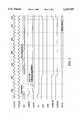
- FIG. 3is a timing diagram that illustrates the generation of address, data, and control signals for a read operation to an ISA peripheral device connected to the integrated processor of FIG. 2.
- FIG. 4is a block diagram that illustrates the connection of several standard 8-bit ISA peripherals and a 16-bit IDE hard drive to the integrated processor of FIG. 2.
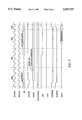
- FIG. 5is a timing diagram that illustrates the data, address, and control signals associated with a 16-bit read operation to the IDE hard drive of FIG. 4.
- FIG. 6is a block diagram that illustrates separate ISA sub bus and IDE data buffers.
- FIG. 7is a block diagram that illustrates an ISA sub bus data buffer cascaded from an IDE data buffer.
- FIG. 8is a block diagram that illustrates an IDE data buffer cascaded from an ISA data buffer.
- FIG. 2a block diagram is shown of a computer system 200 including an integrated processor 210 according to the present invention.
- computer system 200further includes a PCI bus 220 coupled to a PCI peripheral device 222, a data buffer 224, and an address latch 226.
- Computer system 200finally includes an ISA peripheral device 228 and a system memory 230 coupled to integrated processor 210.
- Integrated processor 210includes a CPU core 240 coupled to a memory controller 242, a PCI bus interface unit 244, an ISA sub-bus control unit 246, and an on-chip peripheral device 248 via an internal bus 250.
- CPU core 240implements a model 80486 microprocessor instruction set.
- Bus 250is a model 80486-style local bus. It is understood, however, that CPU core 240 could be configured to implement other microprocessortype instruction sets.
- PCI bus interface unit 244provides an interface between the CPU local bus 250 and PCI bus 220. As such, PCI bus interface unit 244 orchestrates the transfer of data, address, and control signals between CPU local bus 250 and PCI bus 220. Details regarding PCI bus 220 are described within the publication entitled “PCI Local Bus Specification”; PCI Special Interest Group; Hillsboro, Oregon; 1993. This publication is incorporated herein by reference in its entirety.
- On-chip peripheral 248is illustrative of any one of a variety of peripheral devices that may be incorporated within integrated processor 210.
- peripheralssuch as a direct memory access controller, an interrupt controller, and a timer could be included as an integral portion of integrated processor 210.
- Memory controller 242controls the transfer of data between CPU local bus 250 and system memory 230. Since memory controller 242 and CPU core 240 are fabricated on a common integrated circuit, the performance of each is scaled similarly with variations in processor technology.
- ISA sub-bus control unit 246generates a set of signals labeled SUBDIR, SUBEN, and LDEN, along with an I/O read signal IORD, an I/O write signal IOWR, and a chip select signal CS. These signals are referred to collectively as ISA side-band signals.
- the ISA side-band signalsallow data transfers to or from an external ISA peripheral device by controlling the transfer of data and address signals between PCI bus 220, data buffer 224, and address latch 226.
- the ISA sub-bus control unit 246is synchronized with the PCI bus interface unit 244 to ensure proper timing of the side-band signals SUBDIR, SUBEN, LDEN, IOWR, IORD, and CS.
- Data buffer 224is a multi-bit, bidirectional buffer which channels data signals between PCI bus 220 and ISA peripheral device 228.
- Data buffer 224is enabled by the side-band signal SUBEN, and the directionality of data buffer 224 is controlled by the side-band signal SUBDIR. It is noted that for situations in which ISA peripheral device 228 is an 8-bit peripheral, data buffer 224 is an 8-bit buffer and may be coupled to the lower 8-bits (AD[7:0]) of the multiplexed address/data lines of PCI bus 220. For situations in which ISA peripheral device 228 is a 16-bit peripheral, data buffer 224 is a 16-bit buffer and may be coupled to the PCI bus lines AD[15:0].
- Address latch 226is a multi-bit latching circuit which provides address signals from PCI bus 222 to ISA peripheral device 228.
- address latch 226may be up to 32-bit latch; however, it is noted that address latch 226 need only support the number of addressing lines required by the ISA peripheral device.
- Address latch 226is enabled by the loading signal LDEN and is clocked by the PCI clock signal PCICLK.
- Address latch 226may be implemented with a set of type '377 D latches.
- the multiplexed address/data (A/D) lines of PCI bus 220are connected to an input port of address latch 226.
- the clock signal PCICLKis connected to a clock input of address latch 226, and the load enable signal LDEN generated by ISA sub-bus control unit 246 is coupled to the enable input of address latch 226.
- An output port of address latch 226is coupled to an address port of ISA peripheral device 228.
- the multiplexed address/data (A/D) lines of PCI bus 220are additionally coupled to data buffer 224.
- ISA peripheral device 228is an 8-bit device, and thus the low order 8-bits of the multiplexed address/data lines (AD[7:0]) of PCI bus 228 are coupled to data buffer 224.
- a second port of data buffer 224is coupled to a data port of ISA peripheral device 228.
- the data enable signal SUBEN and the data direction signal SUBDIR generated by ISA sub-bus control unit 246are respectively coupled to an enable input and a direction input of data buffer 224. As stated previously, these signals control the enabling and directionality of data buffer 224.
- the chip select signal generated by ISA sub-bus control unit 246is coupled to the chip select input of ISA peripheral device 228, and the I/O read signal IORD and the I/O write signal IOWR are further coupled to ISA peripheral device 228 for controlling the reading and writing of data into and out of ISA peripheral device 228.
- FIG. 3is a timing diagram that illustrates the data, address, and control signals associated with an I/O read operation to ISA peripheral device 228.
- CPU core 240initiates a read cycle to the I/O addressable space to which ISA peripheral device 228 is mapped
- a valid address signalis driven through the PCI bus interface unit 244 and on to the multiplexed address/data lines AD[31:0] of PCI bus 220 during an ISA sub-bus state 302.
- the ISA sub-bus control unit 246asserts the loading signal LDEN.
- the valid address signalis thereby latched into address latch 226 synchronously with the rising edge of the PCI clock signal.
- the chip select signal CSis asserted low by ISA sub-bus control unit 246 to select peripheral device 228. As illustrated in FIG. 3, the chip select signal CS is asserted low throughout the I/O read cycle to ISA peripheral device 228. Upon the rising edge of the loading signal LDEN, a valid address signal is provided at the output of address latch 226 and to the address port of ISA peripheral device 228.
- the I/O read signal IORas well as the enable signal SUBEN and the data direction signal SUBDIR are asserted low.
- the ISA peripheral device 228responsively fetches the data from the requested location, and drives the data through data buffer 224 to the multiplexed address/data lines of PCI bus 220. As illustrated in the figure, the data is driven on the PCI bus 220 during states 306, 308, 310, and 312.
- PCI interface unit 244latches the data into the integrated processor 210. This completes the ISA sub-bus read operation.
- a write operation to ISA peripheral device 228is similar. It is noted that standard ISA-style bus timing is employed for write cycles to ISA peripheral device 228. It is also noted that during a write cycle, the directional signal SUBDIR is complemented to allow opposite flow of data from PCI bus 220 to ISA peripheral device 228.
- FIG. 4a block diagram is shown of another configuration of an integrated processor 210 that employs a high performance integrated processor architecture according to the present invention. It is noted that circuit portions that correspond to those of FIG. 2 are numbered identically. It is further noted that various subunits of integrated processor 210 as illustrated in FIG. 2 (i.e., such as CPU core 240 and PCI bux interface unit 244) have been omitted from the drawing of FIG. 4 for simplicity and clarity.
- FIG. 4The configuration of FIG. 4 is similar to that of FIG. 2; however, the ISA sub-bus control unit 246 of FIG. 4 is capable of controlling a plurality of standard ISA peripherals in addition to an IDE (Integrated Drive Electronics) hard drive 402.
- the standard ISA peripherals illustrated in FIG. 4include a keyboard controller 404, a real time clock (RTC) 406, a modem 408, a serial port 410, a parallel port 412, and a floppy controller 414.
- RTCreal time clock
- the ISA sub-bus control unit 246generates a set of chip select signal (CSG0-CSG3) to select a particular ISA device.
- the chip signals CSG0-CSG3are driven by the ISA sub-bus control unit 246 with an encoded signal which is decoded by a decoder 420 to enable an addressed ISA peripheral bus.
- the ISA sub-bus control unit 246also generates a hard drive data enable signal HDBEN.
- the hard drive data enable signal HDBENis used to enable a data buffer 425 that buffers data between the multiplexed address/data lines AD[31:0] of a PCI bus (i.e., PCI bus 220 of FIG. 2) and the data lines of the IDE hard drive 402. It is noted that since the IDE hard drive 402 is a 16-bit device, the data buffer 425 is a 16-bit buffer.
- FIG. 5is a timing diagram that illustrates the data, address, and control signals associated with an I/O read operation to IDE hard drive 402.
- a valid address signalis driven through the PCI bus interface unit (i.e., unit 244 of FIG. 2) on the multiplexed address/data lines AD[31:0] of PCI bus 220 during an ISA sub-bus state 502.
- the ISA sub-bus control unit 246asserts the loading signal LDEN.
- the valid address signalis thereby latched into address latch 226 synchronously with the rising edge of the PCI clock signal.
- the chip select signals CSG0-CSG3are driven with a predetermined encoded value that corresponds to the IDE hard drive 402.
- the decoder 420decodes the encoded value and responsively asserts a signal at an output line 430 to select the IDE hard drive 402.
- the chip select signals CSG0-CSG3are driven during the entire I/O read cycle.
- a valid address signalis provided at the output of address latch 226 and to an address port 434 of IDE hard drive 402.
- the hard drive data enable signal HDBEN and the data direction signal SUBDIRare asserted low to allow the transfer of data from IDE hard drive 402 through data buffer 425 to the multiplexed address/data lines of PCI bus 220.
- the I/O read signal IORis asserted low by ISA sub-bus control unit 246.
- the IDE hard drive 402responsively fetches the addressed data from the requested location, and drives the data through data buffer 425 to the multiplexed address/data lines of PCI bus 220 during ISA sub-bus state 506.
- PCI interface unit 244(illustrated in FIG. 2) latches the data into the integrated processor 210. This completes the ISA sub-bus read operation to the IDE hard drive 402.
- Read and write operations to keyboard controller 404, RTC 406, modem 408, serial port 410, parallel port 412, and floppy controller 414are accomplished in a manner similar to that described above in conjunction with FIGS. 2 and 3. It is noted, however, that the chip select signals CSG0-CSG3 are driven with a different predetermined encoded value to select different ISA peripheral devices. It is further noted that a write operation to IDE hard drive 402 is also accomplished by driving the ISA side-band signals in accordance with standard ISA-style bus timing. For a write operation, the data direction signal SUBDIR is complemented (with respect to its state during a read cycle).
- FIGS. 6-8illustrate several alternative configurations for coupling data between PCI bus 220 and an IDE hard drive, as well as between PCI bus 220 and a standard 8-bit ISA peripherals.
- FIG. 6illustrates a configuration in which separate ISA sub-bus and IDE data buffers are employed. This configuration is identical to that shown in FIG. 4.
- FIG. 7illustrates a configuration in which the 8-bit ISA sub-bus data is cascaded from the IDE data buffer 425.
- the 8-bit data buffer 224is optional.
- Standard 8-bit ISA peripheralsmay be connected to data buffer 224 at lines 701, and an IDE hard drive may be connected at lines 702.
- a configurationis shown in which the 16-bit IDE data is cascaded from a 16-bit ISA data buffer 810.
- the IDE data buffer 425is optional for this configuration.
- An IDE hard drivemay be connected at lines 812, and a standard ISA peripheral may be connected at lines 814.
- an integrated processor employing a sub-bus control unit as described abovemay also employ a variety of other pin-reducing circuits or techniques.
- the integrated processor 210may be configured to employ the power management message bus as described within the co-pending, commonly assigned patent application entitled "Power Management Message Bus For Integrated Processor”; by Gephardt, et al.; Ser. No. 08/190,280; filed concurrently herewith. This application is incorporated herein by reference in its entirety.
- high performance multiplexed address/data bus 220 of FIG. 2is a PCI standard bus
- other multiplexed high performance busescould be alternatively employed.
- the integrated processor 210 of FIG. 2may incorporate a variety of additional on-chip peripheral devices. It is intended that the following claims be interpreted to embrace all such variations and modifications.
Landscapes
- Engineering & Computer Science (AREA)
- Theoretical Computer Science (AREA)
- General Engineering & Computer Science (AREA)
- Physics & Mathematics (AREA)
- General Physics & Mathematics (AREA)
- Computer Hardware Design (AREA)
- Bus Control (AREA)
Abstract
Description
1. Field of the Invention
This invention relates to integrated processing systems and more particularly to a high performance integrated processor architecture that supports an external derivation of a low performance peripheral bus from a multiplexed peripheral bus.
2. Description of the Relevant Art
FIG. 1 is a block diagram of acomputer system 10 including a microprocessor (CPU) 12, a CPUlocal bus 14 coupled tomicroprocessor 12, and amemory controller 16 and a local busperipheral device 18 coupled to CPUlocal bus 14. Asystem memory 18 is further shown coupled tomemory controller 16. APCI standard bus 20 is coupled to CPUlocal bus 14 through aPCI bus bridge 22, and an ISA (Industry Standard Architecture)bus 24 is coupled to CPUlocal bus 14 throughISA bus bridge 26. A PCIperipheral device 28 is finally shown coupled toPCI bus 20, and an ISAperipheral device 30 is shown coupled toISA bus 24.
The ISAbus 24 of FIG. 1 supports the connection of ISA peripheral devices withincomputer system 10. ISAbus 26 orchestrates the transfer of data, address, and control signals between CPUlocal bus 14 andISA bus 24. Although ISAbus 24 is a relatively low performance bus, the inclusion ofISA bus 24 and ISAbus bridge 26 withincomputer system 10 advantageously allows ISA peripheral devices to be connected within the system. It is noted that this feature is advantageous since a wide variety of ISA compatible peripheral devices are currently available.
The problems outlined above are in large part solved by an integrated processor that employs a high performance integrated processor architecture according to the present invention. In one embodiment, an integrated processor includes a bus interface unit that provides an interface to a high performance peripheral interconnect bus with multiplexed address/data lines. The peripheral interconnect bus, which may be a PCI standard bus, accommodates data transfers between an internal bus of the integrated processor and PCI peripheral devices. The integrated processor further includes a sub-bus control unit that generates a set of side-band control signals that allow the external derivation of a lower performance secondary bus, such as an ISA bus, without requiring a complete set of external pins for the secondary bus on the integrated processor. The derivation of the secondary bus is accomplished with an external data buffer and an external address latch which are controlled by the side-band control signals. Separate address and data lines from the integrated processor for the secondary bus are not required. Accordingly, high performance peripheral devices are supported by the integrated processor as well as lower performance, lower-cost peripherals without a significant increase in the pin-count of the integrated processor. Accordingly, overall cost of the integrated processor is kept low while a wide range of peripheral devices are accommodated.
Broadly speaking, the present invention contemplates a computer system comprising a peripheral bus including a plurality of multiplexed address/data lines, a latch having an input port coupled to a plurality of multiplexed address/data lines, a data buffer having a first port coupled to said plurality of multiplexed address/data lines and an integrated processor. The integrated processor includes a CPU core, a local bus coupled to the CPU core, and a bus interface unit capable of interfacing data, address, and control signals between the local bus and the peripheral bus. The integrated processor further includes a sub-bus bus control unit coupled to the local bus and capable of generating a loading signal indicative of the presence of a valid address on the peripheral bus. A peripheral device is also included having a plurality of addressing lines coupled to an output port of the latch, and a plurality of data lines coupled to a second port of the data buffer.
The present invention further contemplates a method for driving an ISA-style sub-bus externally from an integrated processor, wherein the integrated processor includes a CPU core, a local bus coupled to the CPU core, and a bus interface unit for interfacing data, address, and control signals between the local bus and an external multiplexed peripheral bus. The method comprises the steps of driving a plurality of multiplexed address/data lines of the peripheral bus with a valid address signal, asserting a loading signal when the peripheral bus is driven with the valid address signal, and latching the valid address signal in response to the loading signal. The method further comprises the steps of providing the valid address signal to a peripheral device, providing an I/O transfer request signal to the peripheral device, and providing valid data through said data buffer.
The present invention finally contemplates a computer system comprising a PCI standard configuration peripheral bus including a plurality of multiplexed address/data lines, a latch having an input port coupled to the plurality of multiplexed address/data lines, and a data buffer having a first port coupled to the plurality of multiplexed address/data lines. An integrated processor is also provided including a CPU core, a local bus coupled to the CPU core, and a bus interface unit capable of interfacing data, address, and control signals between the local bus and the PCI standard configuration peripheral bus. The integrated processor also includes an ISA sub-bus control unit coupled to the local bus and capable of generating a loading signal indicative of the presence of a valid address on the PCI standard configuration peripheral bus. A peripheral device is finally provided having a plurality of addressing lines coupled to an output port of the latch, and a plurality of data lines coupled to a second port of the data buffer.
Other objects and advantages of the invention will become apparent upon reading the following detailed description and upon reference to the accompanying drawings in which:
FIG. 1 is a block diagram of a computer system including a high performance PCI peripheral bus and a lower performance ISA peripheral bus.
FIG. 2 is a block diagram of a computer system including an integrated processor architecture in accordance with the present invention.
FIG. 3 is a timing diagram that illustrates the generation of address, data, and control signals for a read operation to an ISA peripheral device connected to the integrated processor of FIG. 2.
FIG. 4 is a block diagram that illustrates the connection of several standard 8-bit ISA peripherals and a 16-bit IDE hard drive to the integrated processor of FIG. 2.
FIG. 5 is a timing diagram that illustrates the data, address, and control signals associated with a 16-bit read operation to the IDE hard drive of FIG. 4.
FIG. 6 is a block diagram that illustrates separate ISA sub bus and IDE data buffers.
FIG. 7 is a block diagram that illustrates an ISA sub bus data buffer cascaded from an IDE data buffer.
FIG. 8 is a block diagram that illustrates an IDE data buffer cascaded from an ISA data buffer.
While the invention is susceptible to various modifications and alternative forms, specific embodiments thereof are shown by way of example in the drawings and will herein be described in detail. It should be understood, however, that the drawings and detailed description thereto are not intended to limit the invention to the particular form disclosed, but on the contrary, the intention is to cover all modifications, equivalents and alternatives falling within the spirit and scope of the present invention as defined by the appended claims.
Referring now to FIG. 2, a block diagram is shown of acomputer system 200 including an integratedprocessor 210 according to the present invention. In addition to integratedprocessor 210,computer system 200 further includes aPCI bus 220 coupled to a PCIperipheral device 222, adata buffer 224, and anaddress latch 226.Computer system 200 finally includes an ISAperipheral device 228 and asystem memory 230 coupled tointegrated processor 210.
PCIbus interface unit 244 provides an interface between the CPUlocal bus 250 andPCI bus 220. As such, PCIbus interface unit 244 orchestrates the transfer of data, address, and control signals between CPUlocal bus 250 andPCI bus 220. Details regardingPCI bus 220 are described within the publication entitled "PCI Local Bus Specification"; PCI Special Interest Group; Hillsboro, Oregon; 1993. This publication is incorporated herein by reference in its entirety.
On-chip peripheral 248 is illustrative of any one of a variety of peripheral devices that may be incorporated withinintegrated processor 210. For example, peripherals such as a direct memory access controller, an interrupt controller, and a timer could be included as an integral portion ofintegrated processor 210.
As will be explained in further detail below, ISAsub-bus control unit 246 generates a set of signals labeled SUBDIR, SUBEN, and LDEN, along with an I/O read signal IORD, an I/O write signal IOWR, and a chip select signal CS. These signals are referred to collectively as ISA side-band signals. The ISA side-band signals allow data transfers to or from an external ISA peripheral device by controlling the transfer of data and address signals betweenPCI bus 220,data buffer 224, andaddress latch 226. The ISAsub-bus control unit 246 is synchronized with the PCIbus interface unit 244 to ensure proper timing of the side-band signals SUBDIR, SUBEN, LDEN, IOWR, IORD, and CS.
Details regarding the data, address, and control signals associated withintegrated processor 210,PCI bus 220,data buffer 224,address latch 226, and ISAperipheral device 228 are next considered. The multiplexed address/data (A/D) lines ofPCI bus 220 are connected to an input port ofaddress latch 226. The clock signal PCICLK is connected to a clock input ofaddress latch 226, and the load enable signal LDEN generated by ISAsub-bus control unit 246 is coupled to the enable input ofaddress latch 226. An output port ofaddress latch 226 is coupled to an address port of ISAperipheral device 228.
The multiplexed address/data (A/D) lines ofPCI bus 220 are additionally coupled todata buffer 224. In the embodiment shown, ISAperipheral device 228 is an 8-bit device, and thus the low order 8-bits of the multiplexed address/data lines (AD[7:0]) ofPCI bus 228 are coupled todata buffer 224. A second port ofdata buffer 224 is coupled to a data port of ISAperipheral device 228. The data enable signal SUBEN and the data direction signal SUBDIR generated by ISAsub-bus control unit 246 are respectively coupled to an enable input and a direction input ofdata buffer 224. As stated previously, these signals control the enabling and directionality ofdata buffer 224. The chip select signal generated by ISAsub-bus control unit 246 is coupled to the chip select input of ISAperipheral device 228, and the I/O read signal IORD and the I/O write signal IOWR are further coupled to ISAperipheral device 228 for controlling the reading and writing of data into and out of ISAperipheral device 228.
Referring next to FIG. 3 in conjunction with FIG. 2, the operation ofcomputer system 200 is next explained. FIG. 3 is a timing diagram that illustrates the data, address, and control signals associated with an I/O read operation to ISAperipheral device 228. WhenCPU core 240 initiates a read cycle to the I/O addressable space to which ISAperipheral device 228 is mapped, a valid address signal is driven through the PCIbus interface unit 244 and on to the multiplexed address/data lines AD[31:0] ofPCI bus 220 during anISA sub-bus state 302. At this time, the ISAsub-bus control unit 246 asserts the loading signal LDEN. The valid address signal is thereby latched intoaddress latch 226 synchronously with the rising edge of the PCI clock signal. At the same time the valid address signal is driven onPCI bus 220, the chip select signal CS is asserted low by ISAsub-bus control unit 246 to selectperipheral device 228. As illustrated in FIG. 3, the chip select signal CS is asserted low throughout the I/O read cycle to ISAperipheral device 228. Upon the rising edge of the loading signal LDEN, a valid address signal is provided at the output ofaddress latch 226 and to the address port of ISAperipheral device 228.
During the next ISAsub-bus state 304, the I/O read signal IOR as well as the enable signal SUBEN and the data direction signal SUBDIR are asserted low. The ISAperipheral device 228 responsively fetches the data from the requested location, and drives the data throughdata buffer 224 to the multiplexed address/data lines ofPCI bus 220. As illustrated in the figure, the data is driven on thePCI bus 220 duringstates sub-bus control unit 246 deasserts the I/O read signal IOR duringstate 314,PCI interface unit 244 latches the data into theintegrated processor 210. This completes the ISA sub-bus read operation.
A write operation to ISAperipheral device 228 is similar. It is noted that standard ISA-style bus timing is employed for write cycles to ISAperipheral device 228. It is also noted that during a write cycle, the directional signal SUBDIR is complemented to allow opposite flow of data fromPCI bus 220 to ISAperipheral device 228.
Referring next to FIG. 4, a block diagram is shown of another configuration of anintegrated processor 210 that employs a high performance integrated processor architecture according to the present invention. It is noted that circuit portions that correspond to those of FIG. 2 are numbered identically. It is further noted that various subunits ofintegrated processor 210 as illustrated in FIG. 2 (i.e., such asCPU core 240 and PCI bux interface unit 244) have been omitted from the drawing of FIG. 4 for simplicity and clarity.
The configuration of FIG. 4 is similar to that of FIG. 2; however, the ISAsub-bus control unit 246 of FIG. 4 is capable of controlling a plurality of standard ISA peripherals in addition to an IDE (Integrated Drive Electronics)hard drive 402. The standard ISA peripherals illustrated in FIG. 4 include akeyboard controller 404, a real time clock (RTC) 406, amodem 408, aserial port 410, aparallel port 412, and afloppy controller 414. As will be explained in greater detail below, the ISAsub-bus control unit 246 generates a set of chip select signal (CSG0-CSG3) to select a particular ISA device. The chip signals CSG0-CSG3 are driven by the ISAsub-bus control unit 246 with an encoded signal which is decoded by adecoder 420 to enable an addressed ISA peripheral bus.
In addition to the data enable signal SUBEN and the data direction SUBDIR, which are generated in a manner similar to that described above in connection with FIG. 2, the ISAsub-bus control unit 246 also generates a hard drive data enable signal HDBEN. The hard drive data enable signal HDBEN is used to enable adata buffer 425 that buffers data between the multiplexed address/data lines AD[31:0] of a PCI bus (i.e.,PCI bus 220 of FIG. 2) and the data lines of the IDEhard drive 402. It is noted that since the IDEhard drive 402 is a 16-bit device, thedata buffer 425 is a 16-bit buffer.
Referring next to FIG. 5 in conjunction with FIG. 4, the operation of the computer system of FIG. 4 is next explained. FIG. 5 is a timing diagram that illustrates the data, address, and control signals associated with an I/O read operation to IDEhard drive 402. When the CPU core initiates a read cycle to the I/O addressable space to which IDEhard drive 402 is mapped, a valid address signal is driven through the PCI bus interface unit (i.e.,unit 244 of FIG. 2) on the multiplexed address/data lines AD[31:0] ofPCI bus 220 during anISA sub-bus state 502. At this time, the ISAsub-bus control unit 246 asserts the loading signal LDEN. The valid address signal is thereby latched intoaddress latch 226 synchronously with the rising edge of the PCI clock signal. At the same time the valid address signal is driven onPCI bus 220, the chip select signals CSG0-CSG3 are driven with a predetermined encoded value that corresponds to the IDEhard drive 402. Thedecoder 420 decodes the encoded value and responsively asserts a signal at anoutput line 430 to select the IDEhard drive 402. As illustrated in FIG. 5, the chip select signals CSG0-CSG3 are driven during the entire I/O read cycle. Upon the rising edge of the loading signal LDEN, a valid address signal is provided at the output ofaddress latch 226 and to anaddress port 434 of IDEhard drive 402. Duringstate 502, the hard drive data enable signal HDBEN and the data direction signal SUBDIR are asserted low to allow the transfer of data from IDEhard drive 402 throughdata buffer 425 to the multiplexed address/data lines ofPCI bus 220.
DuringISA sub-bus state 504, the I/O read signal IOR is asserted low by ISAsub-bus control unit 246. The IDEhard drive 402 responsively fetches the addressed data from the requested location, and drives the data throughdata buffer 425 to the multiplexed address/data lines ofPCI bus 220 during ISAsub-bus state 506. When the ISAsub-bus control unit 246 deasserts the I/O read signal IOR duringstate 508, PCI interface unit 244 (illustrated in FIG. 2) latches the data into theintegrated processor 210. This completes the ISA sub-bus read operation to the IDEhard drive 402.
Read and write operations tokeyboard controller 404,RTC 406,modem 408,serial port 410,parallel port 412, andfloppy controller 414 are accomplished in a manner similar to that described above in conjunction with FIGS. 2 and 3. It is noted, however, that the chip select signals CSG0-CSG3 are driven with a different predetermined encoded value to select different ISA peripheral devices. It is further noted that a write operation to IDEhard drive 402 is also accomplished by driving the ISA side-band signals in accordance with standard ISA-style bus timing. For a write operation, the data direction signal SUBDIR is complemented (with respect to its state during a read cycle).
FIGS. 6-8 illustrate several alternative configurations for coupling data betweenPCI bus 220 and an IDE hard drive, as well as betweenPCI bus 220 and a standard 8-bit ISA peripherals. FIG. 6 illustrates a configuration in which separate ISA sub-bus and IDE data buffers are employed. This configuration is identical to that shown in FIG. 4. FIG. 7 illustrates a configuration in which the 8-bit ISA sub-bus data is cascaded from theIDE data buffer 425. For this configuration, the 8-bit data buffer 224 is optional. Standard 8-bit ISA peripherals may be connected to data buffer 224 atlines 701, and an IDE hard drive may be connected atlines 702. Referring finally to FIG. 8, a configuration is shown in which the 16-bit IDE data is cascaded from a 16-bitISA data buffer 810. TheIDE data buffer 425 is optional for this configuration. An IDE hard drive may be connected atlines 812, and a standard ISA peripheral may be connected atlines 814.
It is noted that an integrated processor employing a sub-bus control unit as described above may also employ a variety of other pin-reducing circuits or techniques. For example, theintegrated processor 210 may be configured to employ the power management message bus as described within the co-pending, commonly assigned patent application entitled "Power Management Message Bus For Integrated Processor"; by Gephardt, et al.; Ser. No. 08/190,280; filed concurrently herewith. This application is incorporated herein by reference in its entirety.
Numerous variations and modifications will become apparent to those skilled in the art once the above disclosure is fully appreciated. For example, although the high performance multiplexed address/data bus 220 of FIG. 2 is a PCI standard bus, other multiplexed high performance buses could be alternatively employed. Furthermore, it is noted that theintegrated processor 210 of FIG. 2 may incorporate a variety of additional on-chip peripheral devices. It is intended that the following claims be interpreted to embrace all such variations and modifications.
Claims (17)
1. A computer system comprising:
a peripheral bus including a plurality of multiplexed address/data lines;
a latch having an input port coupled to said plurality of multiplexed address/data lines;
a data buffer having a first port coupled to said plurality of multiplexed address/data lines;
an integrated processor fabricated on a single integrated circuit and including:
a CPU core;
a local bus coupled to said CPU core;
a bus interface unit configured to interface data, address, and control signals between said local bus and said peripheral bus; and
a sub-bus control unit for generating signals used to control a secondary, non-multiplexed bus external to said integrated processor, wherein said sub-bus control unit is coupled to said bus interface unit and to said latch and is configured to generate a loading signal indicative of the presence of a valid address on said peripheral bus, and wherein said loading signal is provided to said latch for selectively causing said valid address to be latched within said latch; and
a peripheral device compatible with said secondary, non-multiplexed bus, and having a plurality of addressing lines coupled to an output port of said latch, and a plurality of data lines coupled to a second port of said data buffer.
2. The computer system as recited in claim 1 wherein said peripheral bus is a PCI standard configuration bus.
3. The computer system as recited in claim 2 wherein said peripheral device is an ISA standard peripheral device.
4. The computer system as recited in claim 1 wherein said data buffer includes a direction control input line, and wherein said sub-bus control unit is configured to generate a direction control signal that is provided to the direction control input line of said data buffer to control a flow of data through said data buffer.
5. The computer system as recited in claim 4 wherein said sub-bus control unit is further configured to generate an I/O write signal and an I/O read signal, wherein said direction control signal is dependent upon whether said sub-bus control unit asserts said I/O write signal or said I/O read signal.
6. The computer system as recited in claim 5 wherein said I/O read signal is asserted during a read cycle to said peripheral device, and wherein said I/O read signal makes a transition from an asserted state to a deasserted state when valid read data is present on said multiplexed address/data lines.
7. The computer system as recited in claim 4 wherein said sub-bus control unit is further configured to assert a data enable signal that is received by said data buffer to enable the flow of data through said data buffer.
8. The computer system as recited in claim 1 wherein said CPF core implements an 80486 instruction set.
9. The computer system as recited in claim 1 wherein said loading signal is asserted during an address phase of said peripheral bus and wherein said loading signal is deasserted prior to a data phase of said peripheral bus.
10. The computer system as recited in claim 1 wherein said loading signal is provided to an enable control line of said latch.
11. The computer system as recited in claim 10 wherein a peripheral bus clock signal is provided to a clock input line of said latch.
12. The computer system as recited in claim 1 wherein said sub-bus control unit is further configured to assert a select signal for selecting said peripheral device.
13. The computer system as recited in claim 1 further comprising a decoder coupled to said sub-bus control unit, wherein said sub-bus control unit generates an encoded chip select value, and wherein said decoder decodes said encoded chip select value and generates a corresponding chip select signal that is provided to said peripheral device.
14. A computer system comprising:
a PCI standard configuration peripheral bus including a plurality of multiplexed address/data lines;
a latch having an input port coupled to said plurality of multiplexed address/data lines;
a data buffer having a first port coupled to said plurality of multiplexed address/data lines;
an integrated processor fabricated on a single integrated circuit and including:
a CPU core;
a local bus coupled to said CPU core;
a bus interface unit configured to interface data, address, and control signals between said local bus and said PCI standard configuration peripheral bus; and
a ISA sub-bus control unit for generating signals used to control an ISA bus external to said integrated processor, wherein said ISA sub-bus control unit is coupled to said bus interface unit and to said latch and configured to generate a loading signal indicative of the presence of a valid address on said peripheral bus; and
a peripheral device being compatible with said ISA bus, and having a plurality of addressing lines coupled to an output port of said latch, and a plurality of data lines coupled to a second port of said data buffer.
15. The computer system as recited in claim 14 wherein said data buffer includes a direction control input line, and wherein said ISA sub-bus control unit is configured to generate a direction control signal that is provided to the direction control input line of said data buffer to control a flow of data through said data buffer.
16. The computer system as recited in claim 15 wherein said ISA sub-bus control unit is further configured to generate an I/O write signal and an I/O read signal, wherein said direction control signal is dependent upon whether said ISA sub-bus control unit asserts said I/O write signal or said I/O read signal.
17. The computer system as recited in claim 16 wherein said loading signal is asserted during an address phase of said peripheral bus and wherein said loading signal is deasserted prior to a data phase of said peripheral bus.
Priority Applications (3)
| Application Number | Priority Date | Filing Date | Title |
|---|---|---|---|
| US08/190,647US5557757A (en) | 1994-02-02 | 1994-02-02 | High performance integrated processor architecture including a sub-bus control unit for generating signals to control a secondary, non-multiplexed external bus |
| EP95300520AEP0667581A3 (en) | 1994-02-02 | 1995-01-27 | Computer system with peripheral bus |
| JP7012420AJPH07302240A (en) | 1994-02-02 | 1995-01-30 | Computer system and method for extraction of isa-type subbusto outside of integrated processor |
Applications Claiming Priority (1)
| Application Number | Priority Date | Filing Date | Title |
|---|---|---|---|
| US08/190,647US5557757A (en) | 1994-02-02 | 1994-02-02 | High performance integrated processor architecture including a sub-bus control unit for generating signals to control a secondary, non-multiplexed external bus |
Publications (1)
| Publication Number | Publication Date |
|---|---|
| US5557757Atrue US5557757A (en) | 1996-09-17 |
Family
ID=22702202
Family Applications (1)
| Application Number | Title | Priority Date | Filing Date |
|---|---|---|---|
| US08/190,647Expired - LifetimeUS5557757A (en) | 1994-02-02 | 1994-02-02 | High performance integrated processor architecture including a sub-bus control unit for generating signals to control a secondary, non-multiplexed external bus |
Country Status (3)
| Country | Link |
|---|---|
| US (1) | US5557757A (en) |
| EP (1) | EP0667581A3 (en) |
| JP (1) | JPH07302240A (en) |
Cited By (33)
| Publication number | Priority date | Publication date | Assignee | Title |
|---|---|---|---|---|
| US5644734A (en)* | 1995-08-24 | 1997-07-01 | Ncr Corporation | Method and apparatus for multiplexing bus connector signals with sideband signals |
| US5678064A (en)* | 1994-12-01 | 1997-10-14 | International Business Machines Corporation | Local bus-ISA bridge for supporting PIO and third party DMA data transfers to IDE drives |
| US5682484A (en)* | 1995-11-20 | 1997-10-28 | Advanced Micro Devices, Inc. | System and method for transferring data streams simultaneously on multiple buses in a computer system |
| US5692211A (en)* | 1995-09-11 | 1997-11-25 | Advanced Micro Devices, Inc. | Computer system and method having a dedicated multimedia engine and including separate command and data paths |
| US5740387A (en)* | 1995-11-20 | 1998-04-14 | Advanced Micro Devices, Inc. | Computer system having an expansion bus which includes normal and real time modes |
| US5748921A (en)* | 1995-12-11 | 1998-05-05 | Advanced Micro Devices, Inc. | Computer system including a plurality of multimedia devices each having a high-speed memory data channel for accessing system memory |
| US5754801A (en)* | 1995-11-20 | 1998-05-19 | Advanced Micro Devices, Inc. | Computer system having a multimedia bus and comprising a centralized I/O processor which performs intelligent data transfers |
| US5758107A (en)* | 1994-02-14 | 1998-05-26 | Motorola Inc. | System for offloading external bus by coupling peripheral device to data processor through interface logic that emulate the characteristics of the external bus |
| US5778194A (en)* | 1996-04-08 | 1998-07-07 | Symbios, Inc. | Method and apparatus for measuring performance of a computer bus |
| US5784592A (en)* | 1995-09-11 | 1998-07-21 | Advanced Micro Devices, Inc. | Computer system which includes a local expansion bus and a dedicated real-time bus for increased multimedia performance |
| US5809264A (en)* | 1995-04-18 | 1998-09-15 | Hyundai Electronic Industries Co., Ltd. | Interface with device having unusual access time and method thereof |
| US5812800A (en)* | 1995-09-11 | 1998-09-22 | Advanced Micro Devices, Inc. | Computer system which includes a local expansion bus and a dedicated real-time bus and including a multimedia memory for increased multi-media performance |
| US5838930A (en)* | 1995-08-30 | 1998-11-17 | Kabushiki Kaisha Toshiba | Method and apparatus for controlling a command cycle on a bus |
| US5873114A (en)* | 1995-08-18 | 1999-02-16 | Advanced Micro Devices, Inc. | Integrated processor and memory control unit including refresh queue logic for refreshing DRAM during idle cycles |
| US5872940A (en)* | 1996-04-01 | 1999-02-16 | Motorola, Inc. | Programmable read/write access signal and method therefor |
| US5898892A (en)* | 1996-05-17 | 1999-04-27 | Advanced Micro Devices, Inc. | Computer system with a data cache for providing real-time multimedia data to a multimedia engine |
| US5905879A (en)* | 1995-11-20 | 1999-05-18 | Advanced Micro Devices, Inc. | System and method for transferring periodic data streams on a multimedia bus |
| US5926629A (en)* | 1997-02-18 | 1999-07-20 | Advanced Micro Devices, Inc. | Continuously operating interconnection bus |
| US5944806A (en)* | 1997-09-26 | 1999-08-31 | Hewlett-Packard Company | Microprocessor with versatile addressing |
| US5960180A (en)* | 1994-09-07 | 1999-09-28 | Adaptec, Inc. | Host adapter integrated circuit having autoaccess pause |
| US5974492A (en)* | 1997-02-18 | 1999-10-26 | Advanced Micro Devices, Inc. | Method for input/output port replication using an interconnection bus |
| US5974239A (en)* | 1997-06-11 | 1999-10-26 | Micron Electronics, Inc. | Data transfer method for a bus device in a computer system by placing first and second addresses corresponding to a bridge and with the bus device respectively on a bus |
| US5987560A (en)* | 1997-02-18 | 1999-11-16 | Advanced Micro Devices, Inc. | Integrated programmable logic circuit for conditioning received input signals, detecting transitions of conditioned signals, and generating an associated interrupt respectively |
| US6020900A (en)* | 1997-04-14 | 2000-02-01 | International Business Machines Corporation | Video capture method |
| US6044412A (en)* | 1997-10-21 | 2000-03-28 | Vlsi Technology, Inc. | Integrated circuit pin sharing method and apparatus for diverse memory devices by multiplexing subsets of pins in accordance with operation modes |
| US6047349A (en)* | 1997-06-11 | 2000-04-04 | Micron Electronics, Inc. | System for communicating through a computer system bus bridge |
| US6052747A (en)* | 1996-10-15 | 2000-04-18 | Nec Corporation | Microcomputer incorporating peripheral circuits |
| US6081861A (en)* | 1998-06-15 | 2000-06-27 | International Business Machines Corporation | PCI migration support of ISA adapters |
| US6182168B1 (en) | 1997-11-10 | 2001-01-30 | International Business Machines Corporation | Programmable sideband port for generating sideband signal |
| US6233639B1 (en) | 1999-01-04 | 2001-05-15 | International Business Machines Corporation | Memory card utilizing two wire bus |
| US6523082B1 (en)* | 1999-02-25 | 2003-02-18 | Sega Enterprises, Ltd. | Systems having shared memory and buses |
| US6654845B1 (en)* | 2000-07-06 | 2003-11-25 | Intel Corporation | System and method implementing a secondary bus to avoid read data latency |
| US20080183942A1 (en)* | 2005-05-23 | 2008-07-31 | Mtekvision Co., Ltd. | Sharing Memory Interface |
Families Citing this family (1)
| Publication number | Priority date | Publication date | Assignee | Title |
|---|---|---|---|---|
| EP0902372A1 (en)* | 1997-09-13 | 1999-03-17 | Ming-Cheng Lin | PCI I/O interface card |
Citations (6)
| Publication number | Priority date | Publication date | Assignee | Title |
|---|---|---|---|---|
| US4979097A (en)* | 1987-09-04 | 1990-12-18 | Digital Equipment Corporation | Method and apparatus for interconnecting busses in a multibus computer system |
| US5191657A (en)* | 1989-11-09 | 1993-03-02 | Ast Research, Inc. | Microcomputer architecture utilizing an asynchronous bus between microprocessor and industry standard synchronous bus |
| US5255374A (en)* | 1992-01-02 | 1993-10-19 | International Business Machines Corporation | Bus interface logic for computer system having dual bus architecture |
| US5261057A (en)* | 1988-06-30 | 1993-11-09 | Wang Laboratories, Inc. | I/O bus to system interface |
| US5309568A (en)* | 1992-03-16 | 1994-05-03 | Opti, Inc. | Local bus design |
| US5396602A (en)* | 1993-05-28 | 1995-03-07 | International Business Machines Corp. | Arbitration logic for multiple bus computer system |
- 1994
- 1994-02-02USUS08/190,647patent/US5557757A/ennot_activeExpired - Lifetime
- 1995
- 1995-01-27EPEP95300520Apatent/EP0667581A3/ennot_activeWithdrawn
- 1995-01-30JPJP7012420Apatent/JPH07302240A/enactivePending
Patent Citations (6)
| Publication number | Priority date | Publication date | Assignee | Title |
|---|---|---|---|---|
| US4979097A (en)* | 1987-09-04 | 1990-12-18 | Digital Equipment Corporation | Method and apparatus for interconnecting busses in a multibus computer system |
| US5261057A (en)* | 1988-06-30 | 1993-11-09 | Wang Laboratories, Inc. | I/O bus to system interface |
| US5191657A (en)* | 1989-11-09 | 1993-03-02 | Ast Research, Inc. | Microcomputer architecture utilizing an asynchronous bus between microprocessor and industry standard synchronous bus |
| US5255374A (en)* | 1992-01-02 | 1993-10-19 | International Business Machines Corporation | Bus interface logic for computer system having dual bus architecture |
| US5309568A (en)* | 1992-03-16 | 1994-05-03 | Opti, Inc. | Local bus design |
| US5396602A (en)* | 1993-05-28 | 1995-03-07 | International Business Machines Corp. | Arbitration logic for multiple bus computer system |
Cited By (41)
| Publication number | Priority date | Publication date | Assignee | Title |
|---|---|---|---|---|
| US5758107A (en)* | 1994-02-14 | 1998-05-26 | Motorola Inc. | System for offloading external bus by coupling peripheral device to data processor through interface logic that emulate the characteristics of the external bus |
| US6202117B1 (en)* | 1994-09-07 | 2001-03-13 | Adaptec, Inc. | Host adapter integrated circuit having autoaccess pause |
| US5960180A (en)* | 1994-09-07 | 1999-09-28 | Adaptec, Inc. | Host adapter integrated circuit having autoaccess pause |
| US5678064A (en)* | 1994-12-01 | 1997-10-14 | International Business Machines Corporation | Local bus-ISA bridge for supporting PIO and third party DMA data transfers to IDE drives |
| US5809264A (en)* | 1995-04-18 | 1998-09-15 | Hyundai Electronic Industries Co., Ltd. | Interface with device having unusual access time and method thereof |
| US5873114A (en)* | 1995-08-18 | 1999-02-16 | Advanced Micro Devices, Inc. | Integrated processor and memory control unit including refresh queue logic for refreshing DRAM during idle cycles |
| US5644734A (en)* | 1995-08-24 | 1997-07-01 | Ncr Corporation | Method and apparatus for multiplexing bus connector signals with sideband signals |
| US5838930A (en)* | 1995-08-30 | 1998-11-17 | Kabushiki Kaisha Toshiba | Method and apparatus for controlling a command cycle on a bus |
| US5812800A (en)* | 1995-09-11 | 1998-09-22 | Advanced Micro Devices, Inc. | Computer system which includes a local expansion bus and a dedicated real-time bus and including a multimedia memory for increased multi-media performance |
| US5692211A (en)* | 1995-09-11 | 1997-11-25 | Advanced Micro Devices, Inc. | Computer system and method having a dedicated multimedia engine and including separate command and data paths |
| US5784592A (en)* | 1995-09-11 | 1998-07-21 | Advanced Micro Devices, Inc. | Computer system which includes a local expansion bus and a dedicated real-time bus for increased multimedia performance |
| US5682484A (en)* | 1995-11-20 | 1997-10-28 | Advanced Micro Devices, Inc. | System and method for transferring data streams simultaneously on multiple buses in a computer system |
| US5905879A (en)* | 1995-11-20 | 1999-05-18 | Advanced Micro Devices, Inc. | System and method for transferring periodic data streams on a multimedia bus |
| US5740387A (en)* | 1995-11-20 | 1998-04-14 | Advanced Micro Devices, Inc. | Computer system having an expansion bus which includes normal and real time modes |
| US5951664A (en)* | 1995-11-20 | 1999-09-14 | Advanced Micro Devices, Inc. | Computer system having a multimedia bus and including improved time slotting and bus allocation |
| US5754801A (en)* | 1995-11-20 | 1998-05-19 | Advanced Micro Devices, Inc. | Computer system having a multimedia bus and comprising a centralized I/O processor which performs intelligent data transfers |
| US5748921A (en)* | 1995-12-11 | 1998-05-05 | Advanced Micro Devices, Inc. | Computer system including a plurality of multimedia devices each having a high-speed memory data channel for accessing system memory |
| US5872940A (en)* | 1996-04-01 | 1999-02-16 | Motorola, Inc. | Programmable read/write access signal and method therefor |
| US5778194A (en)* | 1996-04-08 | 1998-07-07 | Symbios, Inc. | Method and apparatus for measuring performance of a computer bus |
| US5898892A (en)* | 1996-05-17 | 1999-04-27 | Advanced Micro Devices, Inc. | Computer system with a data cache for providing real-time multimedia data to a multimedia engine |
| US6052747A (en)* | 1996-10-15 | 2000-04-18 | Nec Corporation | Microcomputer incorporating peripheral circuits |
| US5987560A (en)* | 1997-02-18 | 1999-11-16 | Advanced Micro Devices, Inc. | Integrated programmable logic circuit for conditioning received input signals, detecting transitions of conditioned signals, and generating an associated interrupt respectively |
| US6601178B1 (en) | 1997-02-18 | 2003-07-29 | Advanced Micro Devices, Inc. | System power management partitioned across a serial bus |
| US5926629A (en)* | 1997-02-18 | 1999-07-20 | Advanced Micro Devices, Inc. | Continuously operating interconnection bus |
| US6058443A (en)* | 1997-02-18 | 2000-05-02 | Advanced Micro Devices, Inc. | System for partitioning PC chipset functions into logic and port integrated circuits |
| US5974492A (en)* | 1997-02-18 | 1999-10-26 | Advanced Micro Devices, Inc. | Method for input/output port replication using an interconnection bus |
| US6101560A (en)* | 1997-02-18 | 2000-08-08 | Advanced Micro Devices, Inc. | Partitioned PC game port |
| US6012111A (en)* | 1997-02-18 | 2000-01-04 | Advanced Micro Devices, Inc. | PC chipset with integrated clock synthesizer |
| US6020900A (en)* | 1997-04-14 | 2000-02-01 | International Business Machines Corporation | Video capture method |
| US5974239A (en)* | 1997-06-11 | 1999-10-26 | Micron Electronics, Inc. | Data transfer method for a bus device in a computer system by placing first and second addresses corresponding to a bridge and with the bus device respectively on a bus |
| US6047349A (en)* | 1997-06-11 | 2000-04-04 | Micron Electronics, Inc. | System for communicating through a computer system bus bridge |
| US5944806A (en)* | 1997-09-26 | 1999-08-31 | Hewlett-Packard Company | Microprocessor with versatile addressing |
| US6044412A (en)* | 1997-10-21 | 2000-03-28 | Vlsi Technology, Inc. | Integrated circuit pin sharing method and apparatus for diverse memory devices by multiplexing subsets of pins in accordance with operation modes |
| US6182168B1 (en) | 1997-11-10 | 2001-01-30 | International Business Machines Corporation | Programmable sideband port for generating sideband signal |
| US6081861A (en)* | 1998-06-15 | 2000-06-27 | International Business Machines Corporation | PCI migration support of ISA adapters |
| US6385685B1 (en) | 1999-01-04 | 2002-05-07 | International Business Machines Corporation | Memory card utilizing two wire bus |
| US6233639B1 (en) | 1999-01-04 | 2001-05-15 | International Business Machines Corporation | Memory card utilizing two wire bus |
| US6523082B1 (en)* | 1999-02-25 | 2003-02-18 | Sega Enterprises, Ltd. | Systems having shared memory and buses |
| US6654845B1 (en)* | 2000-07-06 | 2003-11-25 | Intel Corporation | System and method implementing a secondary bus to avoid read data latency |
| US20080183942A1 (en)* | 2005-05-23 | 2008-07-31 | Mtekvision Co., Ltd. | Sharing Memory Interface |
| US7827337B2 (en)* | 2005-05-23 | 2010-11-02 | Mtekvision Co., Ltd. | Sharing memory interface |
Also Published As
| Publication number | Publication date |
|---|---|
| JPH07302240A (en) | 1995-11-14 |
| EP0667581A2 (en) | 1995-08-16 |
| EP0667581A3 (en) | 1998-08-05 |
Similar Documents
| Publication | Publication Date | Title |
|---|---|---|
| US5557757A (en) | High performance integrated processor architecture including a sub-bus control unit for generating signals to control a secondary, non-multiplexed external bus | |
| US5596756A (en) | Sub-bus activity detection technique for power management within a computer system | |
| US6272584B1 (en) | System board with consolidated EEPROM module | |
| US6064626A (en) | Peripheral buses for integrated circuit | |
| US6226700B1 (en) | Computer system with bridge logic that includes an internal modular expansion bus and a common master interface for internal master devices | |
| US5819096A (en) | PCI to ISA interrupt protocol converter and selection mechanism | |
| US5555381A (en) | Microcomputer architecture utilizing an asynchronous bus between microprocessor and industry standard synchronous bus | |
| US6012111A (en) | PC chipset with integrated clock synthesizer | |
| US5655142A (en) | High performance derived local bus and computer system employing the same | |
| KR100352224B1 (en) | Direct memory access(dma) transactions on a low pin count bus | |
| US5826048A (en) | PCI bus with reduced number of signals | |
| US5561772A (en) | Expansion bus system for replicating an internal bus as an external bus with logical interrupts replacing physical interrupt lines | |
| US20060190691A1 (en) | Die-to-die interconnect interface and protocol for stacked semiconductor dies | |
| US5519872A (en) | Fast address latch with automatic address incrementing | |
| US6047349A (en) | System for communicating through a computer system bus bridge | |
| US6490638B1 (en) | General purpose bus with programmable timing | |
| US5933613A (en) | Computer system and inter-bus control circuit | |
| US5857085A (en) | Interface device for XT/AT system devices on high speed local bus | |
| KR100449721B1 (en) | Interface for devices having different data bus width and data transfer method using the same | |
| US6088761A (en) | Reduced pin system interface | |
| US6550015B1 (en) | Scalable virtual timer architecture for efficiently implementing multiple hardware timers with minimal silicon overhead | |
| EP0691616A1 (en) | RAM and ROM control unit | |
| US5974239A (en) | Data transfer method for a bus device in a computer system by placing first and second addresses corresponding to a bridge and with the bus device respectively on a bus | |
| CA2008071A1 (en) | Pump bus to avoid indeterminacy in reading variable bit field | |
| US5842041A (en) | Computer system employing a control signal indicative of whether address is within address space of devices on processor local bus |
Legal Events
| Date | Code | Title | Description |
|---|---|---|---|
| AS | Assignment | Owner name:ADVANCED MICRO DEVICES, INC., CALIFORNIA Free format text:ASSIGNMENT OF ASSIGNORS INTEREST;ASSIGNORS:GEPHARDT, DOUGLAS D.;MUDGETT, DAN S.;MACDONALD, JAMES R.;REEL/FRAME:006868/0476 Effective date:19940131 | |
| STCF | Information on status: patent grant | Free format text:PATENTED CASE | |
| FPAY | Fee payment | Year of fee payment:4 | |
| FPAY | Fee payment | Year of fee payment:8 | |
| FPAY | Fee payment | Year of fee payment:12 | |
| AS | Assignment | Owner name:GLOBALFOUNDRIES INC., CAYMAN ISLANDS Free format text:AFFIRMATION OF PATENT ASSIGNMENT;ASSIGNOR:ADVANCED MICRO DEVICES, INC.;REEL/FRAME:023119/0083 Effective date:20090630 | |
| AS | Assignment | Owner name:GLOBALFOUNDRIES U.S. INC., NEW YORK Free format text:RELEASE BY SECURED PARTY;ASSIGNOR:WILMINGTON TRUST, NATIONAL ASSOCIATION;REEL/FRAME:056987/0001 Effective date:20201117 |