US5554570A - Method of forming insulating film - Google Patents
Method of forming insulating filmDownload PDFInfo
- Publication number
- US5554570A US5554570AUS08/370,247US37024795AUS5554570AUS 5554570 AUS5554570 AUS 5554570AUS 37024795 AUS37024795 AUS 37024795AUS 5554570 AUS5554570 AUS 5554570A
- Authority
- US
- United States
- Prior art keywords
- insulating film
- forming
- film
- silicon oxide
- gas
- Prior art date
- Legal status (The legal status is an assumption and is not a legal conclusion. Google has not performed a legal analysis and makes no representation as to the accuracy of the status listed.)
- Expired - Lifetime
Links
Images


Classifications
- H—ELECTRICITY
- H01—ELECTRIC ELEMENTS
- H01L—SEMICONDUCTOR DEVICES NOT COVERED BY CLASS H10
- H01L21/00—Processes or apparatus adapted for the manufacture or treatment of semiconductor or solid state devices or of parts thereof
- H01L21/02—Manufacture or treatment of semiconductor devices or of parts thereof
- H01L21/02104—Forming layers
- H01L21/02107—Forming insulating materials on a substrate
- H01L21/02109—Forming insulating materials on a substrate characterised by the type of layer, e.g. type of material, porous/non-porous, pre-cursors, mixtures or laminates
- H01L21/02112—Forming insulating materials on a substrate characterised by the type of layer, e.g. type of material, porous/non-porous, pre-cursors, mixtures or laminates characterised by the material of the layer
- H01L21/02123—Forming insulating materials on a substrate characterised by the type of layer, e.g. type of material, porous/non-porous, pre-cursors, mixtures or laminates characterised by the material of the layer the material containing silicon
- H01L21/02164—Forming insulating materials on a substrate characterised by the type of layer, e.g. type of material, porous/non-porous, pre-cursors, mixtures or laminates characterised by the material of the layer the material containing silicon the material being a silicon oxide, e.g. SiO2
- C—CHEMISTRY; METALLURGY
- C23—COATING METALLIC MATERIAL; COATING MATERIAL WITH METALLIC MATERIAL; CHEMICAL SURFACE TREATMENT; DIFFUSION TREATMENT OF METALLIC MATERIAL; COATING BY VACUUM EVAPORATION, BY SPUTTERING, BY ION IMPLANTATION OR BY CHEMICAL VAPOUR DEPOSITION, IN GENERAL; INHIBITING CORROSION OF METALLIC MATERIAL OR INCRUSTATION IN GENERAL
- C23C—COATING METALLIC MATERIAL; COATING MATERIAL WITH METALLIC MATERIAL; SURFACE TREATMENT OF METALLIC MATERIAL BY DIFFUSION INTO THE SURFACE, BY CHEMICAL CONVERSION OR SUBSTITUTION; COATING BY VACUUM EVAPORATION, BY SPUTTERING, BY ION IMPLANTATION OR BY CHEMICAL VAPOUR DEPOSITION, IN GENERAL
- C23C16/00—Chemical coating by decomposition of gaseous compounds, without leaving reaction products of surface material in the coating, i.e. chemical vapour deposition [CVD] processes
- C23C16/22—Chemical coating by decomposition of gaseous compounds, without leaving reaction products of surface material in the coating, i.e. chemical vapour deposition [CVD] processes characterised by the deposition of inorganic material, other than metallic material
- C23C16/30—Deposition of compounds, mixtures or solid solutions, e.g. borides, carbides, nitrides
- C23C16/40—Oxides
- C23C16/401—Oxides containing silicon
- C23C16/402—Silicon dioxide
- H—ELECTRICITY
- H01—ELECTRIC ELEMENTS
- H01L—SEMICONDUCTOR DEVICES NOT COVERED BY CLASS H10
- H01L21/00—Processes or apparatus adapted for the manufacture or treatment of semiconductor or solid state devices or of parts thereof
- H01L21/02—Manufacture or treatment of semiconductor devices or of parts thereof
- H01L21/02104—Forming layers
- H01L21/02107—Forming insulating materials on a substrate
- H01L21/02109—Forming insulating materials on a substrate characterised by the type of layer, e.g. type of material, porous/non-porous, pre-cursors, mixtures or laminates
- H01L21/02112—Forming insulating materials on a substrate characterised by the type of layer, e.g. type of material, porous/non-porous, pre-cursors, mixtures or laminates characterised by the material of the layer
- H01L21/02123—Forming insulating materials on a substrate characterised by the type of layer, e.g. type of material, porous/non-porous, pre-cursors, mixtures or laminates characterised by the material of the layer the material containing silicon
- H01L21/02126—Forming insulating materials on a substrate characterised by the type of layer, e.g. type of material, porous/non-porous, pre-cursors, mixtures or laminates characterised by the material of the layer the material containing silicon the material containing Si, O, and at least one of H, N, C, F, or other non-metal elements, e.g. SiOC, SiOC:H or SiONC
- H01L21/0214—Forming insulating materials on a substrate characterised by the type of layer, e.g. type of material, porous/non-porous, pre-cursors, mixtures or laminates characterised by the material of the layer the material containing silicon the material containing Si, O, and at least one of H, N, C, F, or other non-metal elements, e.g. SiOC, SiOC:H or SiONC the material being a silicon oxynitride, e.g. SiON or SiON:H
- H—ELECTRICITY
- H01—ELECTRIC ELEMENTS
- H01L—SEMICONDUCTOR DEVICES NOT COVERED BY CLASS H10
- H01L21/00—Processes or apparatus adapted for the manufacture or treatment of semiconductor or solid state devices or of parts thereof
- H01L21/02—Manufacture or treatment of semiconductor devices or of parts thereof
- H01L21/02104—Forming layers
- H01L21/02107—Forming insulating materials on a substrate
- H01L21/02109—Forming insulating materials on a substrate characterised by the type of layer, e.g. type of material, porous/non-porous, pre-cursors, mixtures or laminates
- H01L21/022—Forming insulating materials on a substrate characterised by the type of layer, e.g. type of material, porous/non-porous, pre-cursors, mixtures or laminates the layer being a laminate, i.e. composed of sublayers, e.g. stacks of alternating high-k metal oxides
- H—ELECTRICITY
- H01—ELECTRIC ELEMENTS
- H01L—SEMICONDUCTOR DEVICES NOT COVERED BY CLASS H10
- H01L21/00—Processes or apparatus adapted for the manufacture or treatment of semiconductor or solid state devices or of parts thereof
- H01L21/02—Manufacture or treatment of semiconductor devices or of parts thereof
- H01L21/02104—Forming layers
- H01L21/02107—Forming insulating materials on a substrate
- H01L21/02109—Forming insulating materials on a substrate characterised by the type of layer, e.g. type of material, porous/non-porous, pre-cursors, mixtures or laminates
- H01L21/02112—Forming insulating materials on a substrate characterised by the type of layer, e.g. type of material, porous/non-porous, pre-cursors, mixtures or laminates characterised by the material of the layer
- H01L21/02123—Forming insulating materials on a substrate characterised by the type of layer, e.g. type of material, porous/non-porous, pre-cursors, mixtures or laminates characterised by the material of the layer the material containing silicon
- H01L21/02126—Forming insulating materials on a substrate characterised by the type of layer, e.g. type of material, porous/non-porous, pre-cursors, mixtures or laminates characterised by the material of the layer the material containing silicon the material containing Si, O, and at least one of H, N, C, F, or other non-metal elements, e.g. SiOC, SiOC:H or SiONC
- H—ELECTRICITY
- H01—ELECTRIC ELEMENTS
- H01L—SEMICONDUCTOR DEVICES NOT COVERED BY CLASS H10
- H01L21/00—Processes or apparatus adapted for the manufacture or treatment of semiconductor or solid state devices or of parts thereof
- H01L21/02—Manufacture or treatment of semiconductor devices or of parts thereof
- H01L21/02104—Forming layers
- H01L21/02107—Forming insulating materials on a substrate
- H01L21/02109—Forming insulating materials on a substrate characterised by the type of layer, e.g. type of material, porous/non-porous, pre-cursors, mixtures or laminates
- H01L21/02205—Forming insulating materials on a substrate characterised by the type of layer, e.g. type of material, porous/non-porous, pre-cursors, mixtures or laminates the layer being characterised by the precursor material for deposition
- H01L21/02208—Forming insulating materials on a substrate characterised by the type of layer, e.g. type of material, porous/non-porous, pre-cursors, mixtures or laminates the layer being characterised by the precursor material for deposition the precursor containing a compound comprising Si
- H01L21/02211—Forming insulating materials on a substrate characterised by the type of layer, e.g. type of material, porous/non-porous, pre-cursors, mixtures or laminates the layer being characterised by the precursor material for deposition the precursor containing a compound comprising Si the compound being a silane, e.g. disilane, methylsilane or chlorosilane
- H—ELECTRICITY
- H01—ELECTRIC ELEMENTS
- H01L—SEMICONDUCTOR DEVICES NOT COVERED BY CLASS H10
- H01L21/00—Processes or apparatus adapted for the manufacture or treatment of semiconductor or solid state devices or of parts thereof
- H01L21/02—Manufacture or treatment of semiconductor devices or of parts thereof
- H01L21/02104—Forming layers
- H01L21/02107—Forming insulating materials on a substrate
- H01L21/02109—Forming insulating materials on a substrate characterised by the type of layer, e.g. type of material, porous/non-porous, pre-cursors, mixtures or laminates
- H01L21/02205—Forming insulating materials on a substrate characterised by the type of layer, e.g. type of material, porous/non-porous, pre-cursors, mixtures or laminates the layer being characterised by the precursor material for deposition
- H01L21/02208—Forming insulating materials on a substrate characterised by the type of layer, e.g. type of material, porous/non-porous, pre-cursors, mixtures or laminates the layer being characterised by the precursor material for deposition the precursor containing a compound comprising Si
- H01L21/02214—Forming insulating materials on a substrate characterised by the type of layer, e.g. type of material, porous/non-porous, pre-cursors, mixtures or laminates the layer being characterised by the precursor material for deposition the precursor containing a compound comprising Si the compound comprising silicon and oxygen
- H01L21/02216—Forming insulating materials on a substrate characterised by the type of layer, e.g. type of material, porous/non-porous, pre-cursors, mixtures or laminates the layer being characterised by the precursor material for deposition the precursor containing a compound comprising Si the compound comprising silicon and oxygen the compound being a molecule comprising at least one silicon-oxygen bond and the compound having hydrogen or an organic group attached to the silicon or oxygen, e.g. a siloxane
- H—ELECTRICITY
- H01—ELECTRIC ELEMENTS
- H01L—SEMICONDUCTOR DEVICES NOT COVERED BY CLASS H10
- H01L21/00—Processes or apparatus adapted for the manufacture or treatment of semiconductor or solid state devices or of parts thereof
- H01L21/02—Manufacture or treatment of semiconductor devices or of parts thereof
- H01L21/02104—Forming layers
- H01L21/02107—Forming insulating materials on a substrate
- H01L21/02225—Forming insulating materials on a substrate characterised by the process for the formation of the insulating layer
- H01L21/0226—Forming insulating materials on a substrate characterised by the process for the formation of the insulating layer formation by a deposition process
- H01L21/02263—Forming insulating materials on a substrate characterised by the process for the formation of the insulating layer formation by a deposition process deposition from the gas or vapour phase
- H01L21/02271—Forming insulating materials on a substrate characterised by the process for the formation of the insulating layer formation by a deposition process deposition from the gas or vapour phase deposition by decomposition or reaction of gaseous or vapour phase compounds, i.e. chemical vapour deposition
- H01L21/02274—Forming insulating materials on a substrate characterised by the process for the formation of the insulating layer formation by a deposition process deposition from the gas or vapour phase deposition by decomposition or reaction of gaseous or vapour phase compounds, i.e. chemical vapour deposition in the presence of a plasma [PECVD]
Definitions
- the present inventionrelates to a method of forming a silicon containing insulating film by the plasma CVD method.
- the silicon containing insulating film formed by the plasma CVD methodhas, in general, the merit of a density that provides a low moisture permeability, and the merit that the amount of moisture in the insulating film is small.
- Such an insulating filmhas often been used as a covering film for an insulating film which has a considerably larger moisture permeability but possesses good step coverage.
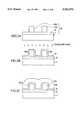
- FIGS. 1A to 1Dare cross sectional views showing an interlayer insulating film having a three layered structure, which is formed by sandwiching the silicon oxide film formed by the thermal CVD method between silicon containing insulating films formed by the plasma CVD method.
- a parallel plate type plasma CVD apparatusis used as the plasma CVD apparatus.
- FIG. 1Ais a cross sectional view showing a structure obtained after interconnection layers are formed and before the silicon containing insulating film is formed by the plasma CVD method.
- a numeral 1denotes a silicon substrate; 2, a backing insulating film on the silicon substrate 1; and 3a and 3b, interconnection layers formed on the backing insulating film 2, spaced from each other by a predetermined distance. These layers constitute a deposition substrate 4.
- the deposition substrate 4is placed in an evacuated chamber, then a reaction gas composed of a mixed gas of SiH 4 +N 2 O is introduced into the chamber for contact with the deposition substrate 4, and then the reaction gas is converted into a plasma by high frequency electric power (RF electric power).
- the N 2 O gasis dissociated into activated nitrogen N* and activated oxygen O* which react with the SiH 4 to form the silicon containing insulating film 5, i.e. a SiO x N y film covering the interconnection layers 3a, 3b.
- refractive index and etching speedboth closely related to denseness of the insulating film etc., can be controlled, and also film stress and the like can be adjusted.
- the refractive indexcan be controlled within a range 1.45 to 2.0 and can therefore be adjusted as required.
- a silicon oxide film (referred to as "NSG film” hereinafter) 6is formed on the silicon containing insulating film 5 by the thermal CVD method using a mixed gas of TEOS+O 3 .
- the reaction gasa mixture of SiH 4 +N 2 O
- a plasma for reactionin the same manner as in FIG. 1B. Consequently, the silicon containing insulating film 7 made of SiO x N y is formed on the silicon oxide film 6.
- the SiO x N y films 5 and 7, formed as described above,have inferior step coverage, they are not suitable for filling the recesses between the narrowly spaced interconnection layers 3a and 3b or for formation on a deposition substrate 4 having an uneven surface. Further, the SiH 4 gas itself is well known as a highly dangerous gas.
- a mixed gas of SiH 4 +N 2 Oinstead of a mixed gas of SiH 4 +N 2 O, a mixed gas of SiH 4 +O 2 , may be used.
- the gaseous mixture of SiH 4 +O 2is not suitable for use in the plasma CVD method since it is highly reactive in gas phase.
- a TEOS reaction gashas recently been used, instead of a reaction gas containing SiH 4 , in the plasma CVD method.
- a reaction gas of TEOS/O 2offers various advantages over a reaction gas of SiH 4 +O 2 , in that the SiO 2 film (silicon containing insulating film) can be formed under any conditions, with high safety, and excellent step coverage of the formed insulating film can be achieved.
- the formed SiO 2 filmcontains carbon and considerable moisture, and it has a high moisture permeability.
- the SiO 2 filmcan be formed under any conditions, it is hard to control the refractive index and the film stress of the insulating film.
- the insulating film formed using TEOS as a reactantlacks flexibility in practical applications. For instance, the refractive index is always about 1.45.
- the interlayer insulating film having a three layered structurewhich is formed by sandwiching tile silicon oxide film formed by the thermal CVD method between silicon containing insulating films formed by the plasma CVD method, the silicon containing insulating film formed from TEOS/O 2 is less conforming to the silicon oxide film, formed as the interlayer film by reaction of TEOS+O 3 , than the silicon containing insulating films 5, 7 formed by reaction of SiH 4 +N 2 O.
- the rate of forming the filmis lower than that of forming the silicon oxide film directly on the silicon substrate and, therefore, unevenness in thickness occurs.
- anomalous growth of the silicon oxide film by the thermal CVD methodis readily caused.
- An object of the present inventionis to provide a method of forming a film by means of the plasma CVD method using a highly safe reaction gas, the method being capable of forming a dense film which is low in moisture and organic residue such as carbon, which has excellent step coverage, which can conform to the silicon oxide film formed by the thermal CVD method, and which allows for control of the refractive index and stress etc. of the formed insulating film.
- a gaseous mixture of an organic compound having Si-H bonds and an oxidizing gasis used as the reaction gas in the plasma CVD method.
- Organic compounds having Si-H bondssuch as alkylsilanes, arylsilanes, alkoxysilanes, chain siloxanes and ring siloxanes are not as reactive as SiH 4 , and thus are safer to use. Such organic compounds are in the liquid state at room temperature and thus are easy to handle.
- the Si-H bonds included in the reaction gasserve to absorb oxygen, generated by plasma decomposition, and O 2 and N 2 O in the oxidizing gas. As a result, the formed insulating film becomes oxygen deficient. Under this condition, since Si is present in excess in the insulating film, the insulating film is dense. Thus, the refractive index can be varied according to the amount of Si. By bringing the insulating film into a Si-excessive condition, affinity of the insulating film for the silicon oxide film formed by the thermal CVD method using the mixed gas of TEOS+O 3 can be improved.
- the refractive index and stress etc. of the formed insulating filmcan be controlled by adjusting the amount of nitrogen contained in the formed insulating film.
- the following, which are suitable for combining with the above organic compounds,can be used as the oxidizing gas. That is, O 2 or N 2 O is mainly used for the organic compounds in the above category 1, and N 2 O is mainly used for the organic compounds in the above categories 2 to 4.
- Oxidizing gasesinclude NO 2 , CO, CO 2 , H 2 O and the like, in addition to O 2 and N 2 O.
- the above organic compoundis combined with at least one of these gases.
- the forming of the film by the plasma CVD methodemploys a highly safe reaction gas and provides a dense silicon containing insulating film low in moisture and organic residues such as carbon, having excellent step coverage, and having good affinity to a silicon oxide film formed by the thermal CVD method. Further, the present invention allows for control of the refractive index, etc. of the silicon containing insulating film.
- FIGS. 1A to 1Dare cross-sectional schematic views showing a conventional method of forming an insulating film
- FIGS. 2A to 2Dare cross-sectional schematic views showing a method of forming an insulating film according to a first embodiment of the present invention
- FIG. 3is a side view, partially in cross-section, of a plasma CVD apparatus used in the method of forming the film according to an embodiment of the present invention
- FIG. 4is a graph of the infrared spectrum for an insulating film formed in accordance with the present invention and illustrating a low moisture content in the silicon-containing insulating film;
- FIG. 5is a graph of the refractive index (ordinate) of the silicon containing insulating film formed by the method of the present invention versus flow rate of N 2 O (abscissa);
- FIG. 6is a graph of the film forming rate (Rd) (ordinate) of the silicon containing insulating film formed by the method of the present invention versus refractive index (abscissa);
- FIG. 7Ais a schematic cross-sectional view of a SiO x N y film formed by the plasma CVD method using a mixed gas of SiH 4 +N 2 O according to a first example;
- FIG. 7Bis a schematic cross-sectional view of the silicon oxide film formed by the plasma CVD method using the mixed gas of SiH 4 +N 2 O according to a second example;
- FIG. 8Ais a schematic cross-sectional view showing a silicon oxide film formed by the thermal CVD method using a mixed gas of TEOS+O 3 , formed on the SiO x N y film shown in FIG.7A according to the first example;
- FIG. 8Bis a schematic cross-sectional view of the silicon oxide film formed by the thermal CVD method using the mixed gas of TEOS+O 3 , formed on the SiO x N y film shown in FIG. 7B according to the second example;
- FIG. 9is a graph of the refractive index and the film forming rate (Rd) of the silicon containing insulating film according to the first example versus the ratio of N 2 O flow rate to SiH 4 flow rate;
- FIG. 10is a graph of the refractive index and the film forming rate of the silicon containing insulating film according to the second example versus the ratio of flow rate of O 2 to flow rate of TEOS containing gas.
- Suitable organic compounds having Si-H bondsinclude:
- the alkyl groupis expressed by the general formula C n H 2 n+1.
- Arylis a generic term for the residue obtained by removing one hydrogen atom from the nucleus of an aromatic hydrocarbon. Suitable aryl groups include phenyl C 6 H 5 --derived from benzene, tolyl CH 3 C 6 H 4 --derived from toluene, xylyl (CH 3 ) 2 C 6 H 3 --derived from xylene, and naphthyl C 10 H 4 --derived from naphthalene.
- the derivativesare organic compounds generated by changes in small portions of the molecules of the aforementioned organic compounds.
- n of the alkyl group C n H 2 n+1be below 5.
- nis 1 or 2.
- Rdenotes an alkyl group, aryl group or a derivative thereof.
- Preferred alkoxysilanesare:
- Trimethoxysilaneis a colorless, transparent liquid having a molecular weight of 122.2 and a boiling point of 86!n. It has an inflammability, but it does not have explosive and hypergolic property like SiH 4 . Thus, it can be handled in the same manner as TEOS.
- Trimethoxysilanehas the formula: ##STR1## 2 Triethoxysilane: (C 2 H 5 O) 3 SiH
- Triethoxysilanehas a boiling point of 131.5° C. and a melting point of -170° C., and has the formula: ##STR2##
- Rdenotes an alkyl group, aryl group or a derivative thereof.
- Tetramethyldisiloxanehas a boiling point of 70°-71° C., and the following formula: ##STR3## 2 Tetraethyldisiloxane: (C 2 H 5 ) 2 HSiOSiH(C 2 H 5 ) 2
- Tetraethyldisiloxanehas the following formula: ##STR4##
- Trimethyltrisiloxanehas the formula: ##STR6## 2 Pentamethyitrisiloxane: (CH 3 ) 2 HSiO((CH 3 )HSiO)SiH(CH 3 ) 2
- Pentamethyltrisiloxanehas the following formula: ##STR7## 3 Triethyltrisiloxane: (C 2 H 5 )H 2 SiO((C 2 H 5 )HSiO)SiH 2 (C 2 H 5 )
- Triethyltrisiloxanehas the following formula: ##STR8## 4 Pentaethyltrisiloxane: (C 2 H 5 )H 2 SiO((C 2 H 5 )HSiO)SiH 2 (C 2 H 5 ) 2
- Ris an alkyl group, aryl group or derivative thereof.
- TMCTShas a boiling point of 134°-135° C. and a melting point of -69° C., and the following formula: ##STR10## 2 TECTS: ((C 2 H 5 )HSiO) 4
- TECTShas a the formula: ##STR11##
- Organic compounds having Si-H bondsthat is, alkylsilanes, arylsilanes, alkoxysilanes and siloxanes, as mentioned above, are not as reactive as SiH and have high safety. They are mainly in liquid phase at room temperature so that they are easy to handle.
- oxidizing gasNO 2 , CO, CO 2 and H 2 O can be used, in addition to O 2 and N 2 O. At least one of these oxidizing gases can be utilized by being combined with one of the organic compounds listed under the above headings (i)(A) to (D). Reaction gases of 83 types can be realized as combinations of the six kinds of the reaction gases. Any one of these reaction gas combinations can be combined with any one of the above organic compounds.
- FIG. 3is a side view showing the structure of the parallel plate type plasma CVD apparatus used in the method of forming the insulating film according to an embodiment of the present invention.
- numeral 21denotes a chamber
- numerals 22a, 22bdenote a pair of electrodes opposing each other.
- the electrode 22awhich is grounded, also serves as a table supporting the deposition substrate 14.
- the electrode 22bto which the high frequency power supply (RF power supply) is connected, also serves as a distributor for the reaction gas.
- the reaction gasis introduced from a gas inlet 24 connected to the distributor 22b.
- the electrode 22ahas a built-in heater (not shown) for heating the deposition substrate 14, and a power supply is connected to the Dower supplying interconnections 25 for the heater.
- An exhaust port 26is connected to an exhausting apparatus (not shown) so as to exhaust spent gas and unreacted reaction gas and to keep the interior of the chamber 21 at a predetermined pressure.
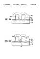
- FIGS. 2A to 2Dare cross sectional views showing the formation of the film by the plasma CVD method according to the first embodiment of the present invention.
- a parallel plate type plasma CVD apparatusis used as the plasma CVD apparatus and trimethoxysilane (CH 3 O) 3 SiH is used as the reaction gas in the following.
- FIG. 2Ais a cross-sectional view showing a structure after the interconnection layers are formed and before the silicon containing insulating film is formed by the plasma CVD method.
- 11denotes the silicon substrate; 12, a backing insulating film made of silicon oxide formed on the silicon substrate 11; and 13a, 13b, interconnection layers formed on the backing insulating film 12 adjacent to each other and spaced at a predetermined distance.
- 11, 12, 13a and 13bconstitute a deposition substrate 14.
- the deposition substrate 14is placed on the electrode 22a in the chamber 21, and then the pressure of the interior of the chamber 21 is reduced. The deposition substrate 14 is then heated and held within a temperature range 300° to 400° C.
- liquid trimethoxysilane at a temperature of 10° C.is vaporized by bubbling argon gas (carrier gas) therethrough at a flow rate of 100 SCCM so that argon gas including trimethoxysilane is generated.
- argon gascarrier gas
- a predetermined flow rate of N 2 O gasis added as the oxidizing gas to the resultant argon gas, and then the mixed gas is introduced into the chamber 21 through the gas inlet. At this time, the pressure in the chamber 21 is held at about 1 Torr.
- the flow rate of N 2 O gaswas varied.
- N 2 Ois dissociated into activated nitrogen N* and activated oxygen O* in the plasma, and these activated species react with the Si-H bonds.
- a SiO x N y film(silicon containing insulating film) is formed to cover the interconnection layers 13a, 13b.
- the Si-H bonds included in the reaction gasserve to react with the oxygen generated in the plasma or with gases such as O 2 and N 2 O in the oxidizing gas.
- the SiO x N y film 15becomes oxygen deficient.
- the SiO x N y film 15is dense.
- the refractive indexcan be varied according to the amount of Si.
- the refractive index and stress etc. of the formed SiO x N y film 15can be controlled by adjusting the amount of nitrogen contained in the SiO x N y film 15.
- the SiO x N y film 15also has good step coverage.
- a silicon oxide film 16is next formed on the SiO x N y film 15 by the thermal CVD method.
- the deposition substrate 14is placed in a normal pressure atmosphere. While the temperature of the substrate 14 is kept at about 400° C., the reaction gas, which is obtained by adding O 3 and O 2 gas (6% O 3 ) to the TEOS carried by the carrier gas, is introduced. The reaction gas is thermally decomposed to form a silicon oxide film 16 on the SiO x N y film 15. Since the backing SiO x N y film 15 has good affinity for the silicon oxide film 16 formed by the thermal CVD method using the mixed gas of TEOS+O 3 , the rate of forming the silicon oxide film 16 is uniform. As a result, abnormal growth of the silicon oxide film 16 can be suppressed, and the silicon oxide film 16 has good step coverage.
- the SiO x N y film (silicon containing insulating film) 17is formed on the silicon oxide film 16 by the plasma CVD method under the same conditions as above.
- an interlayer insulating film having a three layered structureis formed.
- the silicon containing insulating films (SiO x N y films) 15, 17were formed under the following conditions.
- the silicon oxide film 16was formed under the following conditions.
- Reaction gasTEOS(N 2 )+O 3 /O 2 (O 3 concentration is 6%)
- the film formed by application of electric power at 13.56 MHzhas a stress of 5 -10 ⁇ 10 8 dyne/cm 2 (tensile stress), and the film formed by application of electric power at 100 kHz has a stress of 5-10 ⁇ 10 8 dyne/cm 2 (compressive stress).
- the applied frequency used to form the reaction gas plasmais 100 kHz.
- FIG. 4is a view showing the amount of moisture in the SiO x N y films 15, 17 examined by the infrared absorption spectrum method.
- the ordinate axisdenotes the absorption strength shown in proportional scale
- the abscissa axisdenotes the wave number (cm -1 ) shown in proportional scale. No peak indicating moisture appears. Thus, it is noted that the amount of moisture contained in the SiO x N y films 15, 17 is extremely small.
- FIG. 5is a graph illustrating the dependency of the refractive index of the SiO x N y films 15, 17 upon the flow rate of the N 2 O containing gas.
- the magnitude of the refractive indexis used as a criterion for evaluating the denseness of the film, and is also used as a criterion for evaluating the affinity to the silicon oxide film by the thermal CVD method.
- the ordinate axisdenotes the refractive index shown in proportional scale
- the abscissa axisdenotes the flow rate of N 2 O containing gas (SCCM) shown in proportional scale.
- the refractive indexwas inversely proportional to the flow amount of N 2 O containing gas and that the refractive index changed from almost 1.58 to 1.46 with change in the flow rate from 200 to 1200 SCCM.
- the refractive indexcan be controlled by adjusting the flow rate of N 2 O containing gas. The higher the refractive index becomes, the denser the film becomes. As described hereinbelow, the affinity to the silicon oxide film 16 formed by the thermal CVD method also increases.
- FIG. 6is a graph illustrating the effect of the film forming rate of the silicon oxide film, formed by the thermal CVD method, upon the refractive index.
- the ordinate axisdenotes the ratio of the film forming rate (Rd) shown in proportional scale
- the abscissa axisdenotes the refractive index shown in proportional scale.
- the Si-H bonds included in the reaction gasserve to absorb oxygen generated by the plasma or gas such as O 2 and N 2 O in the oxidizing gas.
- the formed silicon containing insulating films 15, 17become short of oxygen.
- the quality of the silicon containing insulating films 15, 17become dense.
- the refractive indexcan be varied according to the amount of Si atoms.
- the refractive index and the stress etc. of the formed SiO x N y , film 15can be controlled by adjusting the amount of nitrogen contained in the formed silicon containing insulating films 15, 17.
- the silicon-containing insulating films 15, 17 formed by the plasma CVD method using the above reaction gascontain low amounts of organic compounds, moisture, carbon etc., and have good step coverage.
- the silicon containing insulating films 15, 17,which are dense and have only a small amount of organic residues, moisture, carbon etc., and have good step coverage, can be formed.
- the refractive index and other properties of the formed silicon containing insulating films 15, 17can also be controlled.
- an interlayer insulating film having the same three layered structure as that of the first embodimentis formed using triethoxysilane (C 2 H 5 O) 3 SiH as the reaction gas.
- the silicon containing insulating films(SiO x N y films) were formed under the following conditions.
- the silicon oxide filmwas formed under the following conditions.
- Reaction gasTEOS(N 2 )+O 3 /O 2 (O 3 concentration is 6%)
- the silicon containing insulating filmswhich have dense film quality and have low amounts of organic residues, moisture, carbon etc., and good step coverage can be formed.
- the refractive index and other properties of the formed silicon-containing insulating filmscan also be controlled.
- an interlayer insulating film having the same structure as that of the first embodimentis formed using tetramethyldisiloxane (CH 3 ) 2 HSiOSiH(CH 3 ) 2 as the reaction gas.
- the silicon-containing insulating films(SiO x N y films) were formed under the following conditions. Other conditions are identical to those conditions described above.
- silicon oxide filmwas formed under the following conditions. Other conditions are identical to those conditions described above.
- Reaction gasTEOS(N 2 )+O 3 /O 2 (O 3 concentration is 6%)
- the silicon-containing insulating filmswhich have dense film quality, have low amounts of organic residues, moisture, carbon etc., and have good step coverage can be formed.
- the refractive index and other properties of the formed silicon-containing insulating filmscan also be controlled.
- FIG. 7Ais a cross-sectional view showing the SiO x Ny film 15a formed by the plasma CVD method using a mixed gas of SiH 4 +N 2 O.
- the sectional shape of the SiO x N y film 15ais emphasized.
- FIG. 8Ashows a cross-section of the silicon oxide film 16a formed on the SiO x N y film 15a by the thermal CVD method using the mixed gas of TEOS+O 3 .
- the silicon-containing insulating film(SiO x N y film) was formed under the following conditions:
- Reaction gasmixed gas of SiH 4 +N 2 O
- silicon oxide film 16awas formed under the following conditions.
- Reaction gasTEOS (N 2 )+O 3 /O 2 (O 3 concentration is 6%)
- the cross-sectional shape of the silicon-containing insulating film 15adoes not show leveling but, rather, is a mushroom shape with the insulating film 15a deposited more thickly on the upper sidewalls of the interconnection layers 13c, 13d. Accordingly, void precursors are formed in the recesses between the interconnection layers 13c, 13d as the interconnection layers 13c, 13d become narrow.
- the left side ordinatedenotes the refractive index in proportional scale and the right side ordinate denotes the ratio of the film forming rate in proportional scale, and the abscissa denotes a ratio of flow rate of N 2 O gas/flow rate of SiH 4 containing gas in proportional scale.
- the film forming rateis almost 0.8 and the affinity to the silicon oxide film 16a by the thermal CVD film formed from the mixed gas of TEOS+O 3 is low if the ratio of flow rate of N 2 O gas/flow rate of SiH 4 containing gas is small, but the film forming rate becomes almost 1 and the affinity to the silicon oxide film 16a becomes higher as the ratio of flow rate increases.
- the silicon oxide film 16ahas better leveling, and the step coverage can be improved.
- FIG. 7Bis a cross-sectional view of a structure obtained after the silicon oxide film (SiO 2 film) 15b is formed by the plasma CVD method using the mixed gas of TEOS+O 2 . Especially, the sectional shape of the silicon oxide film 15b is illustrated with emphasis.
- FIG. 8Bis a cross-sectional view showing a structure obtained after the silicon oxide film 16b is formed on the silicon oxide film 15b by the thermal CVD method using the mixed gas of TEOS+O 3 . Especially, the sectional shape of the silicon oxide film 16b is illustrated with emphasis.
- the silicon oxide film (SiO 2 film) 15bwas formed under the following conditions.
- Reaction gasmixed gas of TEOS+O 2
- silicon oxide film 16bwas formed under the following conditions.
- Reaction gasTEOS(N 2 )+O 3 /O 2 (O 3 concentration is 6%)
- the cross-sectional shape of the silicon oxide film 15bdoes not level as in the case where the mixed gas of SiH 4 +N 2 O is used. But, unlike the case where the mixed gas of SiH 4 +N 2 O is used, the silicon oxide film 15b has the same thickness on both the side walls of the interconnection layers 13e, 13f and the backing insulating film 12b and, therefore, does not show abnormal growth. Consequently, even if the interconnection layers 13e, 13f become narrow, voids in the recesses between the interconnection layers 13e, 13f tend not to form.
- FIG. 10is a view showing dependency of the refractive index and the ratio of the film forming rates (Rd) upon the the ratio of O 2 gas/TEOS containing gas.
- the left side ordinatedenotes the refractive index in proportional scale
- the right side ordinatedenotes the ratio of film forming rate in proportional scale
- the abscissadenotes the ratio of O 2 gas/TEOS containing gas in proportional scale.
- FIG. 10shows that, irrespective of the ratio of O 2 gas/SiH 4 containing gas, the film forming rate is almost 0.8 which is considerably smaller than 1, and that the affinity to the silicon oxide film 16b formed by the thermal CVD method using the mixed gas of TEOS+O 3 is low.
- the silicon oxide film 16bwhen the silicon oxide film 16b is formed by the thermal CVD method using the mixed gas of TEOS+O 3 on the silicon oxide film 15b, which covers the interconnection layers 13e, 13f, the silicon oxide film 16b does not level and therefore voids readily occur in the recesses between the interconnection layers 13e, 13f.
- the silicon oxide film 16has good leveling and excellent step coverage.
- the characteristics of the silicon-containing insulating film 15 or 17 according to the first embodimentcan be compared with the characteristics of the silicon-containing insulating films 15a according to the above first comparison example and the silicon oxide film 15b according to the second comparison example.
Landscapes
- Engineering & Computer Science (AREA)
- Chemical & Material Sciences (AREA)
- Manufacturing & Machinery (AREA)
- General Physics & Mathematics (AREA)
- Physics & Mathematics (AREA)
- Computer Hardware Design (AREA)
- Microelectronics & Electronic Packaging (AREA)
- Power Engineering (AREA)
- Condensed Matter Physics & Semiconductors (AREA)
- Chemical Kinetics & Catalysis (AREA)
- General Chemical & Material Sciences (AREA)
- Inorganic Chemistry (AREA)
- Materials Engineering (AREA)
- Mechanical Engineering (AREA)
- Metallurgy (AREA)
- Organic Chemistry (AREA)
- Formation Of Insulating Films (AREA)
- Chemical Vapour Deposition (AREA)
- Internal Circuitry In Semiconductor Integrated Circuit Devices (AREA)
Abstract
Description
TABLE 1 ______________________________________ molecular formula boiling point(°C.) melting point(°C.) ______________________________________ (CH.sub.3).sub.2 SiH(C.sub.2 H.sub.5) 46 -- ______________________________________
TABLE 2 ______________________________________ molecular formula boiling point(°C.) melting point(°C.) ______________________________________ CH.sub.3 SiH(Cl).sub.2 41-42 -93 (CH.sub.3).sub.2 SiH(Cl) 36 -111 CH.sub.3 SiH(C.sub.2 H.sub.5)Cl 67-68 -- (C.sub.2 H.sub.5).sub.2 SiH(Cl) 143(1.3) -157 ______________________________________
TABLE 3 ______________________________________ molecular formula boiling point(°C.) melting point(°C.) ______________________________________ C.sub.6 H.sub.5 SiH.sub.3 120 -- (C.sub.6 H.sub.5).sub.2 SiH.sub.2 100-101(4) -- (C.sub.6 H.sub.5).sub.3 SiH 160-165(0.4) 42.44 CH.sub.3 (C.sub.6 H.sub.5)SiH.sub.2 139 -- ______________________________________
TABLE 4 ______________________________________ molecular formula boiling point(°C.) melting point(°C.) ______________________________________ (C.sub.6 H.sub.5)SiH(Cl) 143(1.3) -- C.sub.6 H.sub.5 SiH(CH.sub.3)Cl 113(13) 1.054 ______________________________________
TABLE 5 ______________________________________ molecular formula boiling point(°C.) melting point(°C.) ______________________________________ (CH.sub.3 O).sub.3 SiH 86-87 -- (C.sub.2 H.sub.5 O).sub.3 SiH 131.5 -170 ______________________________________
TABLE 6 ______________________________________ first first second embodiment comparison comparison ______________________________________ density of high high low film (denseness) film quality good (same good unstable on side wall as on plane) refractive variable variable invariable index (constant) carbon none or nothing high impurity little moisture low extremely high low moisture low low high permeability step good bad good coverage stress stable stable unstable (no change (change with time) with time) affinity to good good unstable TEOS/O.sub.3 APCVD NSG (surface (Rd = 1.0) (Rd = 0.7-1.0) (Rd = 0.7-0.8) dependency) safety high low high ______________________________________
Claims (19)
Applications Claiming Priority (2)
| Application Number | Priority Date | Filing Date | Title |
|---|---|---|---|
| JP6006381AJP2899600B2 (en) | 1994-01-25 | 1994-01-25 | Film formation method |
| JP6-006381 | 1994-01-25 |
Publications (1)
| Publication Number | Publication Date |
|---|---|
| US5554570Atrue US5554570A (en) | 1996-09-10 |
Family
ID=11636813
Family Applications (1)
| Application Number | Title | Priority Date | Filing Date |
|---|---|---|---|
| US08/370,247Expired - LifetimeUS5554570A (en) | 1994-01-25 | 1995-01-09 | Method of forming insulating film |
Country Status (3)
| Country | Link |
|---|---|
| US (1) | US5554570A (en) |
| EP (1) | EP0664560A3 (en) |
| JP (1) | JP2899600B2 (en) |
Cited By (87)
| Publication number | Priority date | Publication date | Assignee | Title |
|---|---|---|---|---|
| US5733818A (en)* | 1995-10-18 | 1998-03-31 | Nec Corporation | Method for fabricating semiconductor device with planarization step using CMP |
| US5883015A (en)* | 1997-07-03 | 1999-03-16 | Mosel Vitelic Inc. | Method for using oxygen plasma treatment on a dielectric layer |
| US5981375A (en)* | 1996-07-11 | 1999-11-09 | Oki Electric Industry Co., Ltd. | Method of manufacturing a semiconductor device |
| US6054379A (en)* | 1998-02-11 | 2000-04-25 | Applied Materials, Inc. | Method of depositing a low k dielectric with organo silane |
| US6086952A (en)* | 1998-06-15 | 2000-07-11 | Applied Materials, Inc. | Chemical vapor deposition of a copolymer of p-xylylene and a multivinyl silicon/oxygen comonomer |
| US6147009A (en)* | 1998-06-29 | 2000-11-14 | International Business Machines Corporation | Hydrogenated oxidized silicon carbon material |
| US6149987A (en)* | 1998-04-07 | 2000-11-21 | Applied Materials, Inc. | Method for depositing low dielectric constant oxide films |
| US6221755B1 (en)* | 1998-12-04 | 2001-04-24 | Canon Sales Co., Inc. | Film formation method and manufacturing method of semiconductor device |
| US6225236B1 (en)* | 1998-02-12 | 2001-05-01 | Canon Sales Co., Inc. | Method for reforming undercoating surface and method for production of semiconductor device |
| US6245690B1 (en)* | 1998-11-04 | 2001-06-12 | Applied Materials, Inc. | Method of improving moisture resistance of low dielectric constant films |
| US6255718B1 (en) | 1995-02-28 | 2001-07-03 | Chip Express Corporation | Laser ablateable material |
| US6287990B1 (en)* | 1998-02-11 | 2001-09-11 | Applied Materials, Inc. | CVD plasma assisted low dielectric constant films |
| US6303523B2 (en)* | 1998-02-11 | 2001-10-16 | Applied Materials, Inc. | Plasma processes for depositing low dielectric constant films |
| US20010055672A1 (en)* | 2000-02-08 | 2001-12-27 | Todd Michael A. | Low dielectric constant materials and processes |
| WO2002001627A1 (en)* | 2000-06-26 | 2002-01-03 | Hitachi, Ltd. | Semiconductor device and method manufacturing the same |
| US6352945B1 (en) | 1998-02-05 | 2002-03-05 | Asm Japan K.K. | Silicone polymer insulation film on semiconductor substrate and method for forming the film |
| US6362115B1 (en) | 1998-12-09 | 2002-03-26 | Applied Materials, Inc. | In-situ generation of p-xylyiene from liquid precursors |
| US6383955B1 (en)* | 1998-02-05 | 2002-05-07 | Asm Japan K.K. | Silicone polymer insulation film on semiconductor substrate and method for forming the film |
| US6399489B1 (en) | 1999-11-01 | 2002-06-04 | Applied Materials, Inc. | Barrier layer deposition using HDP-CVD |
| US20020086109A1 (en)* | 1997-06-09 | 2002-07-04 | Nec Corporation | Silica insulation film with a reduced dielectric constant and method of forming the same |
| US6432846B1 (en)* | 1999-02-02 | 2002-08-13 | Asm Japan K.K. | Silicone polymer insulation film on semiconductor substrate and method for forming the film |
| US20020189716A1 (en)* | 2001-01-16 | 2002-12-19 | Walter Savich | Deposition and thermal diffusion of borides and carbides of refractory metals |
| US20030017347A1 (en)* | 2001-07-18 | 2003-01-23 | Nec Corporation | Silicon oxide layer reduced in dangling bonds through treatment with hypofluorous acid, process for growing silicon oxide layer and method for deactivating dangling bonds therein |
| US6514880B2 (en) | 1998-02-05 | 2003-02-04 | Asm Japan K.K. | Siloxan polymer film on semiconductor substrate and method for forming same |
| US6531714B1 (en)* | 1994-12-30 | 2003-03-11 | Sgs-Thomson Microelectronics S.R.L. | Process for the production of a semiconductor device having better interface adhesion between dielectric layers |
| US20030049388A1 (en)* | 2001-09-10 | 2003-03-13 | Seon-Mee Cho | Silicon carbide deposited by high density plasma chemical-vapor deposition with bias |
| US6573196B1 (en)* | 2000-08-12 | 2003-06-03 | Applied Materials Inc. | Method of depositing organosilicate layers |
| US20030119336A1 (en)* | 1998-02-05 | 2003-06-26 | Nobuo Matsuki | Insulation film on semiconductor substrate and method for forming same |
| US20030124859A1 (en)* | 1998-09-29 | 2003-07-03 | Applied Materials, Inc. | CVD plasma assisted low dielectric constant films |
| US6593655B1 (en) | 1998-05-29 | 2003-07-15 | Dow Corning Corporation | Method for producing hydrogenated silicon oxycarbide films having low dielectric constant |
| US6593247B1 (en) | 1998-02-11 | 2003-07-15 | Applied Materials, Inc. | Method of depositing low k films using an oxidizing plasma |
| US20030139035A1 (en)* | 2001-12-14 | 2003-07-24 | Applied Materials, Inc. | Low dielectric (low k) barrier films with oxygen doping by plasma-enhanced chemical vapor deposition (pecvd) |
| US20030148223A1 (en)* | 2001-02-23 | 2003-08-07 | Applied Materials, Inc. | Method of depositing low dielectric constant silicon carbide layers |
| US20030194495A1 (en)* | 2002-04-11 | 2003-10-16 | Applied Materials, Inc. | Crosslink cyclo-siloxane compound with linear bridging group to form ultra low k dielectric |
| US20030211244A1 (en)* | 2002-04-11 | 2003-11-13 | Applied Materials, Inc. | Reacting an organosilicon compound with an oxidizing gas to form an ultra low k dielectric |
| US6656837B2 (en) | 2001-10-11 | 2003-12-02 | Applied Materials, Inc. | Method of eliminating photoresist poisoning in damascene applications |
| US6660656B2 (en) | 1998-02-11 | 2003-12-09 | Applied Materials Inc. | Plasma processes for depositing low dielectric constant films |
| US20030232495A1 (en)* | 2002-05-08 | 2003-12-18 | Farhad Moghadam | Methods and apparatus for E-beam treatment used to fabricate integrated circuit devices |
| US6667553B2 (en) | 1998-05-29 | 2003-12-23 | Dow Corning Corporation | H:SiOC coated substrates |
| US20040029400A1 (en)* | 1998-02-11 | 2004-02-12 | Applied Materials, Inc. | Method of decreasing the K value in SIOC layer deposited by chemical vapor deposition |
| US6709721B2 (en) | 2001-03-28 | 2004-03-23 | Applied Materials Inc. | Purge heater design and process development for the improvement of low k film properties |
| US20040056326A1 (en)* | 2002-09-20 | 2004-03-25 | Texas Instruments Incorporated | Method and structure for controlling surface properties of dielectric layers in a thin film component for improved trimming |
| US20040067308A1 (en)* | 2002-10-07 | 2004-04-08 | Applied Materials, Inc. | Two-layer film for next generation damascene barrier application with good oxidation resistance |
| US20040089894A1 (en)* | 2002-03-19 | 2004-05-13 | Fujitsu Limited | Semiconductor device and method of manufacturing the same |
| US20040101633A1 (en)* | 2002-05-08 | 2004-05-27 | Applied Materials, Inc. | Method for forming ultra low k films using electron beam |
| US6750141B2 (en) | 2001-03-28 | 2004-06-15 | Applied Materials Inc. | Silicon carbide cap layers for low dielectric constant silicon oxide layers |
| US6753270B1 (en) | 2000-08-04 | 2004-06-22 | Applied Materials Inc. | Process for depositing a porous, low dielectric constant silicon oxide film |
| US6753258B1 (en) | 2000-11-03 | 2004-06-22 | Applied Materials Inc. | Integration scheme for dual damascene structure |
| US6759327B2 (en) | 2001-10-09 | 2004-07-06 | Applied Materials Inc. | Method of depositing low k barrier layers |
| US6762127B2 (en) | 2001-08-23 | 2004-07-13 | Yves Pierre Boiteux | Etch process for dielectric materials comprising oxidized organo silane materials |
| US20040152338A1 (en)* | 2003-01-31 | 2004-08-05 | Applied Materials, Inc. | Method for depositing a low dielectric constant film |
| US20040156987A1 (en)* | 2002-05-08 | 2004-08-12 | Applied Materials, Inc. | Ultra low dielectric materials based on hybrid system of linear silicon precursor and organic porogen by plasma-enhanced chemical vapor deposition (PECVD) |
| US20040175929A1 (en)* | 2003-03-07 | 2004-09-09 | Applied Materials, Inc. | Method of improving interlayer adhesion |
| US20040234688A1 (en)* | 2002-04-16 | 2004-11-25 | Vinita Singh | Use of cyclic siloxanes for hardness improvement |
| US20040253777A1 (en)* | 2001-08-30 | 2004-12-16 | Hidenori Miyoshi | Method and apparatus for forming film |
| US20040253378A1 (en)* | 2003-06-12 | 2004-12-16 | Applied Materials, Inc. | Stress reduction of SIOC low k film by addition of alkylenes to OMCTS based processes |
| US6835669B2 (en)* | 2000-07-21 | 2004-12-28 | Canon Sales Co., Inc. | Film forming method, semiconductor device and semiconductor device manufacturing method |
| US20050037153A1 (en)* | 2003-08-14 | 2005-02-17 | Applied Materials, Inc. | Stress reduction of sioc low k films |
| US20050042889A1 (en)* | 2001-12-14 | 2005-02-24 | Albert Lee | Bi-layer approach for a hermetic low dielectric constant layer for barrier applications |
| US20050042858A1 (en)* | 2003-01-13 | 2005-02-24 | Lihua Li | Method of improving stability in low k barrier layers |
| US20050077597A1 (en)* | 2003-10-10 | 2005-04-14 | Tokyo Electron Limited | Method and system for treating a dielectric film |
| US6881683B2 (en) | 1998-02-05 | 2005-04-19 | Asm Japan K.K. | Insulation film on semiconductor substrate and method for forming same |
| US6890850B2 (en) | 2001-12-14 | 2005-05-10 | Applied Materials, Inc. | Method of depositing dielectric materials in damascene applications |
| US6903007B1 (en)* | 1995-06-07 | 2005-06-07 | Advanced Micro Devices, Inc. | Process for forming bottom anti-reflection coating for semiconductor fabrication photolithography which inhibits photoresist footing |
| US6905981B1 (en) | 2000-11-24 | 2005-06-14 | Asm Japan K.K. | Low-k dielectric materials and processes |
| US20050214457A1 (en)* | 2004-03-29 | 2005-09-29 | Applied Materials, Inc. | Deposition of low dielectric constant films by N2O addition |
| US20050215072A1 (en)* | 2003-10-10 | 2005-09-29 | Tokyo Electron Limited | Method and system for treating a dielectric film |
| US6974766B1 (en) | 1998-10-01 | 2005-12-13 | Applied Materials, Inc. | In situ deposition of a low κ dielectric layer, barrier layer, etch stop, and anti-reflective coating for damascene application |
| US7030041B2 (en) | 2004-03-15 | 2006-04-18 | Applied Materials Inc. | Adhesion improvement for low k dielectrics |
| US20060086850A1 (en)* | 2004-06-30 | 2006-04-27 | Cohen Douglas J | Lifting lid crusher |
| US20070117310A1 (en)* | 2005-03-15 | 2007-05-24 | Micron Technology, Inc. | Multiple deposition for integration of spacers in pitch multiplication process |
| US7229911B2 (en) | 2004-04-19 | 2007-06-12 | Applied Materials, Inc. | Adhesion improvement for low k dielectrics to conductive materials |
| US20070134435A1 (en)* | 2005-12-13 | 2007-06-14 | Ahn Sang H | Method to improve the ashing/wet etch damage resistance and integration stability of low dielectric constant films |
| US20070155189A1 (en)* | 2006-01-04 | 2007-07-05 | Promos Technologies Pte. Ltd. | Use of TEOS oxides in integrated circuit fabrication processes |
| US7288205B2 (en) | 2004-07-09 | 2007-10-30 | Applied Materials, Inc. | Hermetic low dielectric constant layer for barrier applications |
| US7297376B1 (en) | 2006-07-07 | 2007-11-20 | Applied Materials, Inc. | Method to reduce gas-phase reactions in a PECVD process with silicon and organic precursors to deposit defect-free initial layers |
| US20090093070A1 (en)* | 2005-08-25 | 2009-04-09 | Seiko Epson Corporation | Capacitor, method of manufacturing the same, method of manufacturing ferroelectric memory device, method of manufacturing actuator, and method of manufacturing liquid jet head |
| US20110092077A1 (en)* | 2006-03-31 | 2011-04-21 | Huiwen Xu | Method to minimize wet etch undercuts and provide pore sealing of extreme low k (k<2.5) dielectrics |
| US20120015113A1 (en)* | 2010-07-13 | 2012-01-19 | Applied Materials, Inc. | Methods for forming low stress dielectric films |
| US8123968B2 (en) | 2005-08-25 | 2012-02-28 | Round Rock Research, Llc | Multiple deposition for integration of spacers in pitch multiplication process |
| CN102446753A (en)* | 2011-09-29 | 2012-05-09 | 上海华力微电子有限公司 | Method for controlling reflectivity and extinction coefficient of dielectric anti-reflection film required by photoresist |
| CN102543715A (en)* | 2012-02-28 | 2012-07-04 | 上海华力微电子有限公司 | Production method of nitrogen-free dielectric antireflective film |
| US8216949B2 (en) | 2004-09-02 | 2012-07-10 | Round Rock Research, Llc | Method for integrated circuit fabrication using pitch multiplication |
| US10304900B2 (en) | 2015-04-02 | 2019-05-28 | Microsoft Technology Licensing, Llc | Bending semiconductor chip in molds having radially varying curvature |
| US10373995B2 (en) | 2014-09-19 | 2019-08-06 | Microsoft Technology Licensing, Llc | Image sensor bending using tension |
| US10515801B2 (en) | 2007-06-04 | 2019-12-24 | Micron Technology, Inc. | Pitch multiplication using self-assembling materials |
| CN113841263A (en)* | 2019-04-25 | 2021-12-24 | 应用材料公司 | Moisture barrier film with low refractive index and low water vapor transmission |
Families Citing this family (11)
| Publication number | Priority date | Publication date | Assignee | Title |
|---|---|---|---|---|
| JP3495116B2 (en)* | 1994-10-31 | 2004-02-09 | 東レ・ダウコーニング・シリコーン株式会社 | Water repellent thin film and method for producing the same |
| JP3061255B2 (en)* | 1995-08-18 | 2000-07-10 | キヤノン販売株式会社 | Film formation method |
| US5939141A (en)* | 1997-08-11 | 1999-08-17 | The United States Of America As Represented By The Administrator Of The National Aeronautics And Space Administration | Waterproof silicone coatings of thermal insulation and vaporization method |
| JP3348084B2 (en) | 1999-12-28 | 2002-11-20 | キヤノン販売株式会社 | Film forming method and semiconductor device |
| DE10010286A1 (en)* | 2000-02-25 | 2001-09-13 | Infineon Technologies Ag | Method for filling depressions in a surface of a semiconductor structure and a semiconductor structure filled in this way |
| JP2001291713A (en)* | 2000-04-07 | 2001-10-19 | Canon Sales Co Inc | Film forming method and semiconductor device |
| JP3600507B2 (en)* | 2000-05-18 | 2004-12-15 | キヤノン販売株式会社 | Semiconductor device and manufacturing method thereof |
| JP2002009069A (en) | 2000-06-22 | 2002-01-11 | Canon Sales Co Inc | Method for forming film |
| KR100486333B1 (en)* | 2000-07-21 | 2005-04-29 | 가부시끼가이샤 한도따이 프로세스 켄큐쇼 | Semiconductor apparatus and method of manufacturing the same |
| JP3701626B2 (en)* | 2001-12-06 | 2005-10-05 | キヤノン販売株式会社 | Manufacturing method of semiconductor device |
| JP4535505B2 (en)* | 2006-02-10 | 2010-09-01 | ルネサスエレクトロニクス株式会社 | Manufacturing method of semiconductor device |
Citations (6)
| Publication number | Priority date | Publication date | Assignee | Title |
|---|---|---|---|---|
| US4708884A (en)* | 1984-07-11 | 1987-11-24 | American Telephone And Telegraph Company, At&T Bell Laboratories | Low temperature deposition of silicon oxides for device fabrication |
| US5051380A (en)* | 1989-12-27 | 1991-09-24 | Semiconductor Process Laboratory Co., Ltd. | Process for producing semiconductor device |
| US5120680A (en)* | 1990-07-19 | 1992-06-09 | At&T Bell Laboratories | Method for depositing dielectric layers |
| US5124014A (en)* | 1990-02-27 | 1992-06-23 | At&T Bell Laboratories | Method of forming oxide layers by bias ECR plasma deposition |
| US5378510A (en)* | 1992-05-28 | 1995-01-03 | Polar Materials Inc. | Methods and apparatus for depositing barrier coatings |
| US5403630A (en)* | 1992-10-27 | 1995-04-04 | Kabushiki Kaisha Toshiba | Vapor-phase growth method for forming S2 O2 films |
Family Cites Families (11)
| Publication number | Priority date | Publication date | Assignee | Title |
|---|---|---|---|---|
| US4282268A (en)* | 1977-05-04 | 1981-08-04 | Rca Corporation | Method of depositing a silicon oxide dielectric layer |
| US4168330A (en)* | 1977-10-13 | 1979-09-18 | Rca Corporation | Method of depositing a silicon oxide layer |
| JPS60245128A (en)* | 1984-05-18 | 1985-12-04 | Canon Inc | Forming method of accumulated film |
| JPS61234531A (en)* | 1985-04-11 | 1986-10-18 | Canon Inc | Method for making silicon oxide |
| ZA884511B (en)* | 1987-07-15 | 1989-03-29 | Boc Group Inc | Method of plasma enhanced silicon oxide deposition |
| US4877641A (en)* | 1988-05-31 | 1989-10-31 | Olin Corporation | Process for plasma depositing silicon nitride and silicon dioxide films onto a substrate |
| JPH0793298B2 (en)* | 1988-10-11 | 1995-10-09 | 日本電気株式会社 | Method for forming semiconductor device |
| JP2800210B2 (en)* | 1988-12-19 | 1998-09-21 | セイコーエプソン株式会社 | Method for manufacturing field effect transistor |
| US5040046A (en)* | 1990-10-09 | 1991-08-13 | Micron Technology, Inc. | Process for forming highly conformal dielectric coatings in the manufacture of integrated circuits and product produced thereby |
| JP2884968B2 (en)* | 1992-11-17 | 1999-04-19 | 東亞合成株式会社 | Method for manufacturing silicon oxide film |
| JPH06283519A (en)* | 1993-03-26 | 1994-10-07 | Kawasaki Steel Corp | Manufacture of semiconductor device |
- 1994
- 1994-01-25JPJP6006381Apatent/JP2899600B2/ennot_activeExpired - Fee Related
- 1995
- 1995-01-09USUS08/370,247patent/US5554570A/ennot_activeExpired - Lifetime
- 1995-01-18EPEP95300293Apatent/EP0664560A3/ennot_activeWithdrawn
Patent Citations (6)
| Publication number | Priority date | Publication date | Assignee | Title |
|---|---|---|---|---|
| US4708884A (en)* | 1984-07-11 | 1987-11-24 | American Telephone And Telegraph Company, At&T Bell Laboratories | Low temperature deposition of silicon oxides for device fabrication |
| US5051380A (en)* | 1989-12-27 | 1991-09-24 | Semiconductor Process Laboratory Co., Ltd. | Process for producing semiconductor device |
| US5124014A (en)* | 1990-02-27 | 1992-06-23 | At&T Bell Laboratories | Method of forming oxide layers by bias ECR plasma deposition |
| US5120680A (en)* | 1990-07-19 | 1992-06-09 | At&T Bell Laboratories | Method for depositing dielectric layers |
| US5378510A (en)* | 1992-05-28 | 1995-01-03 | Polar Materials Inc. | Methods and apparatus for depositing barrier coatings |
| US5403630A (en)* | 1992-10-27 | 1995-04-04 | Kabushiki Kaisha Toshiba | Vapor-phase growth method for forming S2 O2 films |
Non-Patent Citations (2)
| Title |
|---|
| Process Technology, vol. 1, pp. 182 190, Wolf et al. Silicon Processing for the VLSI Era.* |
| Process Technology, vol. 1, pp. 182-190, Wolf et al. Silicon Processing for the VLSI Era. |
Cited By (185)
| Publication number | Priority date | Publication date | Assignee | Title |
|---|---|---|---|---|
| US6531714B1 (en)* | 1994-12-30 | 2003-03-11 | Sgs-Thomson Microelectronics S.R.L. | Process for the production of a semiconductor device having better interface adhesion between dielectric layers |
| US6255718B1 (en) | 1995-02-28 | 2001-07-03 | Chip Express Corporation | Laser ablateable material |
| US6903007B1 (en)* | 1995-06-07 | 2005-06-07 | Advanced Micro Devices, Inc. | Process for forming bottom anti-reflection coating for semiconductor fabrication photolithography which inhibits photoresist footing |
| US5733818A (en)* | 1995-10-18 | 1998-03-31 | Nec Corporation | Method for fabricating semiconductor device with planarization step using CMP |
| US5981375A (en)* | 1996-07-11 | 1999-11-09 | Oki Electric Industry Co., Ltd. | Method of manufacturing a semiconductor device |
| US7056839B2 (en)* | 1997-06-09 | 2006-06-06 | Nec Corporation | Method of forming a silica insulation film with a reduced dielectric constant |
| US20020086109A1 (en)* | 1997-06-09 | 2002-07-04 | Nec Corporation | Silica insulation film with a reduced dielectric constant and method of forming the same |
| US5883015A (en)* | 1997-07-03 | 1999-03-16 | Mosel Vitelic Inc. | Method for using oxygen plasma treatment on a dielectric layer |
| US6559520B2 (en) | 1998-02-05 | 2003-05-06 | Asm Japan K.K. | Siloxan polymer film on semiconductor substrate |
| US20030119336A1 (en)* | 1998-02-05 | 2003-06-26 | Nobuo Matsuki | Insulation film on semiconductor substrate and method for forming same |
| US6383955B1 (en)* | 1998-02-05 | 2002-05-07 | Asm Japan K.K. | Silicone polymer insulation film on semiconductor substrate and method for forming the film |
| US6653719B2 (en) | 1998-02-05 | 2003-11-25 | Asm Japan K.K. | Silicone polymer insulation film on semiconductor substrate |
| US6852650B2 (en) | 1998-02-05 | 2005-02-08 | Asm Japan K.K. | Insulation film on semiconductor substrate and method for forming same |
| US6514880B2 (en) | 1998-02-05 | 2003-02-04 | Asm Japan K.K. | Siloxan polymer film on semiconductor substrate and method for forming same |
| US6455445B2 (en) | 1998-02-05 | 2002-09-24 | Asm Japan K.K. | Silicone polymer insulation film on semiconductor substrate and method for forming the film |
| US6881683B2 (en) | 1998-02-05 | 2005-04-19 | Asm Japan K.K. | Insulation film on semiconductor substrate and method for forming same |
| US6410463B1 (en) | 1998-02-05 | 2002-06-25 | Asm Japan K.K. | Method for forming film with low dielectric constant on semiconductor substrate |
| US6352945B1 (en) | 1998-02-05 | 2002-03-05 | Asm Japan K.K. | Silicone polymer insulation film on semiconductor substrate and method for forming the film |
| US6730593B2 (en) | 1998-02-11 | 2004-05-04 | Applied Materials Inc. | Method of depositing a low K dielectric with organo silane |
| US6660663B1 (en) | 1998-02-11 | 2003-12-09 | Applied Materials Inc. | Computer readable medium for holding a program for performing plasma-assisted CVD of low dielectric constant films formed from organosilane compounds |
| US6054379A (en)* | 1998-02-11 | 2000-04-25 | Applied Materials, Inc. | Method of depositing a low k dielectric with organo silane |
| US6348725B2 (en) | 1998-02-11 | 2002-02-19 | Applied Materials, Inc. | Plasma processes for depositing low dielectric constant films |
| US7651725B2 (en)* | 1998-02-11 | 2010-01-26 | Applied Materials, Inc. | Low dielectric constant film produced from silicon compounds comprising silicon-carbon bond |
| US6784119B2 (en) | 1998-02-11 | 2004-08-31 | Applied Materials Inc. | Method of decreasing the K value in SIOC layer deposited by chemical vapor deposition |
| US20040166665A1 (en)* | 1998-02-11 | 2004-08-26 | Applied Materials, Inc. | Method of decreasing the K value in SIOC layer deposited by chemical vapor deposition |
| US6072227A (en)* | 1998-02-11 | 2000-06-06 | Applied Materials, Inc. | Low power method of depositing a low k dielectric with organo silane |
| US20080044557A1 (en)* | 1998-02-11 | 2008-02-21 | Wai-Fan Yau | Low dielectric constant film produced from silicon compounds comprising silicon-carbon bond |
| US20040147109A1 (en)* | 1998-02-11 | 2004-07-29 | Applied Materials, Inc. | Low dielectric constant film produced from silicon compounds comprising silicon-carbon bond |
| US6869896B2 (en) | 1998-02-11 | 2005-03-22 | Applied Materials, Inc. | Plasma processes for depositing low dielectric constant films |
| US6511903B1 (en) | 1998-02-11 | 2003-01-28 | Applied Materials, Inc. | Method of depositing a low k dielectric with organo silane |
| US6303523B2 (en)* | 1998-02-11 | 2001-10-16 | Applied Materials, Inc. | Plasma processes for depositing low dielectric constant films |
| US7560377B2 (en) | 1998-02-11 | 2009-07-14 | Applied Materials, Inc. | Plasma processes for depositing low dielectric constant films |
| US6287990B1 (en)* | 1998-02-11 | 2001-09-11 | Applied Materials, Inc. | CVD plasma assisted low dielectric constant films |
| US20050156317A1 (en)* | 1998-02-11 | 2005-07-21 | Applied Materials, Inc. | Low dielectric constant film produced from silicon compounds comprising silicon-carbon bonds |
| US6734115B2 (en) | 1998-02-11 | 2004-05-11 | Applied Materials Inc. | Plasma processes for depositing low dielectric constant films |
| US6537929B1 (en) | 1998-02-11 | 2003-03-25 | Applied Materials, Inc. | CVD plasma assisted low dielectric constant films |
| US6541282B1 (en) | 1998-02-11 | 2003-04-01 | Applied Materials, Inc. | Plasma processes for depositing low dielectric constant films |
| US20040082199A1 (en)* | 1998-02-11 | 2004-04-29 | Applied Materials, Inc. | Plasma processes for depositing low dielectric constant films |
| US6562690B1 (en)* | 1998-02-11 | 2003-05-13 | Applied Materials, Inc. | Plasma processes for depositing low dielectric constant films |
| US6930061B2 (en) | 1998-02-11 | 2005-08-16 | Applied Materials Inc. | Plasma processes for depositing low dielectric constant films |
| US20050191846A1 (en)* | 1998-02-11 | 2005-09-01 | David Cheung | Plasma processes for depositing low dielectric constant films |
| US20040038545A1 (en)* | 1998-02-11 | 2004-02-26 | Applied Materials, Inc. | Plasma processes for depositing low dielectric constant films |
| US20040029400A1 (en)* | 1998-02-11 | 2004-02-12 | Applied Materials, Inc. | Method of decreasing the K value in SIOC layer deposited by chemical vapor deposition |
| US6593247B1 (en) | 1998-02-11 | 2003-07-15 | Applied Materials, Inc. | Method of depositing low k films using an oxidizing plasma |
| US6596655B1 (en) | 1998-02-11 | 2003-07-22 | Applied Materials Inc. | Plasma processes for depositing low dielectric constant films |
| US6660656B2 (en) | 1998-02-11 | 2003-12-09 | Applied Materials Inc. | Plasma processes for depositing low dielectric constant films |
| US20080061439A1 (en)* | 1998-02-11 | 2008-03-13 | Wai-Fan Yau | Low dielectric constant film produced from silicon compounds comprising silicon-carbon bond |
| US7074708B2 (en) | 1998-02-11 | 2006-07-11 | Applied Materials, Inc. | Method of decreasing the k value in sioc layer deposited by chemical vapor deposition |
| US20080064225A1 (en)* | 1998-02-11 | 2008-03-13 | Wai-Fan Yau | Low dielectric constant film produced from silicon compounds comprising silicon-carbon bond |
| US6225236B1 (en)* | 1998-02-12 | 2001-05-01 | Canon Sales Co., Inc. | Method for reforming undercoating surface and method for production of semiconductor device |
| US6523494B1 (en) | 1998-04-07 | 2003-02-25 | Applied Materials, Inc. | Apparatus for depositing low dielectric constant oxide film |
| US6149987A (en)* | 1998-04-07 | 2000-11-21 | Applied Materials, Inc. | Method for depositing low dielectric constant oxide films |
| US6593655B1 (en) | 1998-05-29 | 2003-07-15 | Dow Corning Corporation | Method for producing hydrogenated silicon oxycarbide films having low dielectric constant |
| US6667553B2 (en) | 1998-05-29 | 2003-12-23 | Dow Corning Corporation | H:SiOC coated substrates |
| US6086952A (en)* | 1998-06-15 | 2000-07-11 | Applied Materials, Inc. | Chemical vapor deposition of a copolymer of p-xylylene and a multivinyl silicon/oxygen comonomer |
| US6147009A (en)* | 1998-06-29 | 2000-11-14 | International Business Machines Corporation | Hydrogenated oxidized silicon carbon material |
| US6497963B1 (en) | 1998-06-29 | 2002-12-24 | International Business Machines Corporation | Hydrogenated oxidized silicon carbon material |
| US6724086B1 (en) | 1998-06-29 | 2004-04-20 | International Business Machines Corporation | Hydrogenated oxidized silicon carbon material |
| US6800571B2 (en) | 1998-09-29 | 2004-10-05 | Applied Materials Inc. | CVD plasma assisted low dielectric constant films |
| US7205249B2 (en) | 1998-09-29 | 2007-04-17 | Applied Materials, Inc. | CVD plasma assisted low dielectric constant films |
| US20030124859A1 (en)* | 1998-09-29 | 2003-07-03 | Applied Materials, Inc. | CVD plasma assisted low dielectric constant films |
| US20050059264A1 (en)* | 1998-09-29 | 2005-03-17 | David Cheung | CVD plasma assisted low dielectric constant films |
| US7470611B2 (en) | 1998-10-01 | 2008-12-30 | Applied Materials, Inc. | In situ deposition of a low K dielectric layer, barrier layer, etch stop, and anti-reflective coating for damascene application |
| US6974766B1 (en) | 1998-10-01 | 2005-12-13 | Applied Materials, Inc. | In situ deposition of a low κ dielectric layer, barrier layer, etch stop, and anti-reflective coating for damascene application |
| US7670945B2 (en) | 1998-10-01 | 2010-03-02 | Applied Materials, Inc. | In situ deposition of a low κ dielectric layer, barrier layer, etch stop, and anti-reflective coating for damascene application |
| US6245690B1 (en)* | 1998-11-04 | 2001-06-12 | Applied Materials, Inc. | Method of improving moisture resistance of low dielectric constant films |
| US20030054667A1 (en)* | 1998-11-04 | 2003-03-20 | Applied Materials, Inc. | Method of improving moisture resistance of low dielectric constant films |
| US6448187B2 (en) | 1998-11-04 | 2002-09-10 | Applied Materials, Inc. | Method of improving moisture resistance of low dielectric constant films |
| US6743737B2 (en) | 1998-11-04 | 2004-06-01 | Applied Materials, Inc. | Method of improving moisture resistance of low dielectric constant films |
| US6221755B1 (en)* | 1998-12-04 | 2001-04-24 | Canon Sales Co., Inc. | Film formation method and manufacturing method of semiconductor device |
| US6362115B1 (en) | 1998-12-09 | 2002-03-26 | Applied Materials, Inc. | In-situ generation of p-xylyiene from liquid precursors |
| US6432846B1 (en)* | 1999-02-02 | 2002-08-13 | Asm Japan K.K. | Silicone polymer insulation film on semiconductor substrate and method for forming the film |
| US6399489B1 (en) | 1999-11-01 | 2002-06-04 | Applied Materials, Inc. | Barrier layer deposition using HDP-CVD |
| US6713390B2 (en) | 1999-11-01 | 2004-03-30 | Applied Materials Inc. | Barrier layer deposition using HDP-CVD |
| US7144620B2 (en) | 2000-02-08 | 2006-12-05 | Asm Japan K.K. | Process for depositing low dielectric constant materials |
| US20070032676A1 (en)* | 2000-02-08 | 2007-02-08 | Todd Michael A | Process for depositing low dielectric constant materials |
| US6733830B2 (en) | 2000-02-08 | 2004-05-11 | Asm Japan K.K. | Processes for depositing low dielectric constant materials |
| US20010055672A1 (en)* | 2000-02-08 | 2001-12-27 | Todd Michael A. | Low dielectric constant materials and processes |
| US20040161617A1 (en)* | 2000-02-08 | 2004-08-19 | Todd Michael A. | Process for depositing low dielectric constant materials |
| US7544827B2 (en) | 2000-02-08 | 2009-06-09 | Asm Japan K.K. | Process for depositing low dielectric constant materials |
| WO2002001627A1 (en)* | 2000-06-26 | 2002-01-03 | Hitachi, Ltd. | Semiconductor device and method manufacturing the same |
| US6835669B2 (en)* | 2000-07-21 | 2004-12-28 | Canon Sales Co., Inc. | Film forming method, semiconductor device and semiconductor device manufacturing method |
| US6753270B1 (en) | 2000-08-04 | 2004-06-22 | Applied Materials Inc. | Process for depositing a porous, low dielectric constant silicon oxide film |
| US6573196B1 (en)* | 2000-08-12 | 2003-06-03 | Applied Materials Inc. | Method of depositing organosilicate layers |
| US6753258B1 (en) | 2000-11-03 | 2004-06-22 | Applied Materials Inc. | Integration scheme for dual damascene structure |
| US6905981B1 (en) | 2000-11-24 | 2005-06-14 | Asm Japan K.K. | Low-k dielectric materials and processes |
| US20020189716A1 (en)* | 2001-01-16 | 2002-12-19 | Walter Savich | Deposition and thermal diffusion of borides and carbides of refractory metals |
| US20030148223A1 (en)* | 2001-02-23 | 2003-08-07 | Applied Materials, Inc. | Method of depositing low dielectric constant silicon carbide layers |
| US7200460B2 (en) | 2001-02-23 | 2007-04-03 | Applied Materials, Inc. | Method of depositing low dielectric constant silicon carbide layers |
| US6709721B2 (en) | 2001-03-28 | 2004-03-23 | Applied Materials Inc. | Purge heater design and process development for the improvement of low k film properties |
| US6750141B2 (en) | 2001-03-28 | 2004-06-15 | Applied Materials Inc. | Silicon carbide cap layers for low dielectric constant silicon oxide layers |
| US6896861B2 (en)* | 2001-07-18 | 2005-05-24 | Nec Corporation | Silicon oxide layer reduced in dangling bonds through treatment with hypofluorous acid, process for growing silicon oxide layer and method for deactivating dangling bonds therein |
| US20030017347A1 (en)* | 2001-07-18 | 2003-01-23 | Nec Corporation | Silicon oxide layer reduced in dangling bonds through treatment with hypofluorous acid, process for growing silicon oxide layer and method for deactivating dangling bonds therein |
| US6762127B2 (en) | 2001-08-23 | 2004-07-13 | Yves Pierre Boiteux | Etch process for dielectric materials comprising oxidized organo silane materials |
| US20040253777A1 (en)* | 2001-08-30 | 2004-12-16 | Hidenori Miyoshi | Method and apparatus for forming film |
| US20030049388A1 (en)* | 2001-09-10 | 2003-03-13 | Seon-Mee Cho | Silicon carbide deposited by high density plasma chemical-vapor deposition with bias |
| US6926926B2 (en) | 2001-09-10 | 2005-08-09 | Applied Materials, Inc. | Silicon carbide deposited by high density plasma chemical-vapor deposition with bias |
| US20070042610A1 (en)* | 2001-10-09 | 2007-02-22 | Li-Qun Xia | Method of depositing low k barrier layers |
| US20040198070A1 (en)* | 2001-10-09 | 2004-10-07 | Li-Qun Xia | Method of depositing low K barrier layers |
| US7319068B2 (en) | 2001-10-09 | 2008-01-15 | Applied Materials, Inc. | Method of depositing low k barrier layers |
| US7125813B2 (en) | 2001-10-09 | 2006-10-24 | Applied Materials, Inc. | Method of depositing low K barrier layers |
| US6759327B2 (en) | 2001-10-09 | 2004-07-06 | Applied Materials Inc. | Method of depositing low k barrier layers |
| US20060205206A1 (en)* | 2001-10-11 | 2006-09-14 | Applied Materials, Inc. | Method of eliminating photoresist poisoning in damascene applications |
| US20040106278A1 (en)* | 2001-10-11 | 2004-06-03 | Applied Materials, Inc. | Method of eliminating photoresist poisoning in damascene applications |
| US6656837B2 (en) | 2001-10-11 | 2003-12-02 | Applied Materials, Inc. | Method of eliminating photoresist poisoning in damascene applications |
| US7034409B2 (en) | 2001-10-11 | 2006-04-25 | Applied Materials Inc. | Method of eliminating photoresist poisoning in damascene applications |
| US7091137B2 (en) | 2001-12-14 | 2006-08-15 | Applied Materials | Bi-layer approach for a hermetic low dielectric constant layer for barrier applications |
| US7151053B2 (en) | 2001-12-14 | 2006-12-19 | Applied Materials, Inc. | Method of depositing dielectric materials including oxygen-doped silicon carbide in damascene applications |
| US6838393B2 (en) | 2001-12-14 | 2005-01-04 | Applied Materials, Inc. | Method for producing semiconductor including forming a layer containing at least silicon carbide and forming a second layer containing at least silicon oxygen carbide |
| US7745328B2 (en) | 2001-12-14 | 2010-06-29 | Applied Materials, Inc. | Low dielectric (low k) barrier films with oxygen doping by plasma-enhanced chemical vapor deposition (PECVD) |
| US20050042889A1 (en)* | 2001-12-14 | 2005-02-24 | Albert Lee | Bi-layer approach for a hermetic low dielectric constant layer for barrier applications |
| US20090053902A1 (en)* | 2001-12-14 | 2009-02-26 | Kang Sub Yim | Low dielectric (low k) barrier films with oxygen doping by plasma-enhanced chemical vapor deposition (pecvd) |
| US7157384B2 (en) | 2001-12-14 | 2007-01-02 | Applied Materials, Inc. | Low dielectric (low k) barrier films with oxygen doping by plasma-enhanced chemical vapor deposition (PECVD) |
| US20030139035A1 (en)* | 2001-12-14 | 2003-07-24 | Applied Materials, Inc. | Low dielectric (low k) barrier films with oxygen doping by plasma-enhanced chemical vapor deposition (pecvd) |
| US7465659B2 (en) | 2001-12-14 | 2008-12-16 | Applied Materials, Inc. | Low dielectric (low k) barrier films with oxygen doping by plasma-enhanced chemical vapor deposition (PECVD) |
| US20060246737A1 (en)* | 2001-12-14 | 2006-11-02 | Yim Kang S | New low dielectric (low k) barrier films with oxygen doping by plasma-enhanced chemical vapor deposition (pecvd) |
| US6890850B2 (en) | 2001-12-14 | 2005-05-10 | Applied Materials, Inc. | Method of depositing dielectric materials in damascene applications |
| US7528432B2 (en)* | 2002-03-19 | 2009-05-05 | Fujitsu Microelectronics Limited | Semiconductor device having a capacitor and protection insulating films for same |
| US20040089894A1 (en)* | 2002-03-19 | 2004-05-13 | Fujitsu Limited | Semiconductor device and method of manufacturing the same |
| US20030211244A1 (en)* | 2002-04-11 | 2003-11-13 | Applied Materials, Inc. | Reacting an organosilicon compound with an oxidizing gas to form an ultra low k dielectric |
| US20030194495A1 (en)* | 2002-04-11 | 2003-10-16 | Applied Materials, Inc. | Crosslink cyclo-siloxane compound with linear bridging group to form ultra low k dielectric |
| US20040234688A1 (en)* | 2002-04-16 | 2004-11-25 | Vinita Singh | Use of cyclic siloxanes for hardness improvement |
| US20030232495A1 (en)* | 2002-05-08 | 2003-12-18 | Farhad Moghadam | Methods and apparatus for E-beam treatment used to fabricate integrated circuit devices |
| US20050153073A1 (en)* | 2002-05-08 | 2005-07-14 | Applied Materials, Inc. | Method for forming ultra low k films using electron beam |
| US7422774B2 (en) | 2002-05-08 | 2008-09-09 | Applied Materials, Inc. | Method for forming ultra low k films using electron beam |
| US20070275569A1 (en)* | 2002-05-08 | 2007-11-29 | Farhad Moghadam | Methods and apparatus for e-beam treatment used to fabricate integrated circuit devices |
| US7256139B2 (en) | 2002-05-08 | 2007-08-14 | Applied Materials, Inc. | Methods and apparatus for e-beam treatment used to fabricate integrated circuit devices |
| US20050130404A1 (en)* | 2002-05-08 | 2005-06-16 | Applied Materials, Inc. | Methods and apparatus for e-beam treatment used to fabricate integrated circuit devices |
| US7060330B2 (en) | 2002-05-08 | 2006-06-13 | Applied Materials, Inc. | Method for forming ultra low k films using electron beam |
| US20040101633A1 (en)* | 2002-05-08 | 2004-05-27 | Applied Materials, Inc. | Method for forming ultra low k films using electron beam |
| US20040156987A1 (en)* | 2002-05-08 | 2004-08-12 | Applied Materials, Inc. | Ultra low dielectric materials based on hybrid system of linear silicon precursor and organic porogen by plasma-enhanced chemical vapor deposition (PECVD) |
| US7056560B2 (en) | 2002-05-08 | 2006-06-06 | Applies Materials Inc. | Ultra low dielectric materials based on hybrid system of linear silicon precursor and organic porogen by plasma-enhanced chemical vapor deposition (PECVD) |
| US6936551B2 (en) | 2002-05-08 | 2005-08-30 | Applied Materials Inc. | Methods and apparatus for E-beam treatment used to fabricate integrated circuit devices |
| US6818966B2 (en) | 2002-09-20 | 2004-11-16 | Texas Instruments Incorporated | Method and structure for controlling surface properties of dielectric layers in a thin film component for improved trimming |
| US20040056326A1 (en)* | 2002-09-20 | 2004-03-25 | Texas Instruments Incorporated | Method and structure for controlling surface properties of dielectric layers in a thin film component for improved trimming |
| US20040067308A1 (en)* | 2002-10-07 | 2004-04-08 | Applied Materials, Inc. | Two-layer film for next generation damascene barrier application with good oxidation resistance |
| US7749563B2 (en) | 2002-10-07 | 2010-07-06 | Applied Materials, Inc. | Two-layer film for next generation damascene barrier application with good oxidation resistance |
| US20050042858A1 (en)* | 2003-01-13 | 2005-02-24 | Lihua Li | Method of improving stability in low k barrier layers |
| US7049249B2 (en) | 2003-01-13 | 2006-05-23 | Applied Materials | Method of improving stability in low k barrier layers |
| US20040152338A1 (en)* | 2003-01-31 | 2004-08-05 | Applied Materials, Inc. | Method for depositing a low dielectric constant film |
| US6897163B2 (en) | 2003-01-31 | 2005-05-24 | Applied Materials, Inc. | Method for depositing a low dielectric constant film |
| US6913992B2 (en) | 2003-03-07 | 2005-07-05 | Applied Materials, Inc. | Method of modifying interlayer adhesion |
| US8569166B2 (en) | 2003-03-07 | 2013-10-29 | Applied Materials, Inc. | Methods of modifying interlayer adhesion |
| US7960294B2 (en) | 2003-03-07 | 2011-06-14 | Applied Materials, Inc. | Method of modifying interlayer adhesion |
| US20040175929A1 (en)* | 2003-03-07 | 2004-09-09 | Applied Materials, Inc. | Method of improving interlayer adhesion |
| US7226876B2 (en) | 2003-03-07 | 2007-06-05 | Applied Materials, Inc. | Method of modifying interlayer adhesion |
| US7563728B2 (en) | 2003-03-07 | 2009-07-21 | Applied Materials, Inc. | Methods of modifying interlayer adhesion |
| US20040253378A1 (en)* | 2003-06-12 | 2004-12-16 | Applied Materials, Inc. | Stress reduction of SIOC low k film by addition of alkylenes to OMCTS based processes |
| US20050037153A1 (en)* | 2003-08-14 | 2005-02-17 | Applied Materials, Inc. | Stress reduction of sioc low k films |
| US7553769B2 (en)* | 2003-10-10 | 2009-06-30 | Tokyo Electron Limited | Method for treating a dielectric film |
| US20050215072A1 (en)* | 2003-10-10 | 2005-09-29 | Tokyo Electron Limited | Method and system for treating a dielectric film |
| US20050077597A1 (en)* | 2003-10-10 | 2005-04-14 | Tokyo Electron Limited | Method and system for treating a dielectric film |
| US20080076262A1 (en)* | 2003-10-10 | 2008-03-27 | Tokyo Electron Limited | Method and system for treating a dielectric film |
| US7345000B2 (en) | 2003-10-10 | 2008-03-18 | Tokyo Electron Limited | Method and system for treating a dielectric film |
| US7459404B2 (en) | 2004-03-15 | 2008-12-02 | Applied Materials, Inc. | Adhesion improvement for low k dielectrics |
| US7030041B2 (en) | 2004-03-15 | 2006-04-18 | Applied Materials Inc. | Adhesion improvement for low k dielectrics |
| US20050214457A1 (en)* | 2004-03-29 | 2005-09-29 | Applied Materials, Inc. | Deposition of low dielectric constant films by N2O addition |
| US7229911B2 (en) | 2004-04-19 | 2007-06-12 | Applied Materials, Inc. | Adhesion improvement for low k dielectrics to conductive materials |
| US20060086850A1 (en)* | 2004-06-30 | 2006-04-27 | Cohen Douglas J | Lifting lid crusher |
| US7288205B2 (en) | 2004-07-09 | 2007-10-30 | Applied Materials, Inc. | Hermetic low dielectric constant layer for barrier applications |
| US8216949B2 (en) | 2004-09-02 | 2012-07-10 | Round Rock Research, Llc | Method for integrated circuit fabrication using pitch multiplication |
| WO2006091264A1 (en)* | 2005-02-18 | 2006-08-31 | Tokyo Electron Limited | Method and system for treating a dielectric film |
| US20110117743A1 (en)* | 2005-03-15 | 2011-05-19 | Round Rock Research, Llc | Multiple deposition for integration of spacers in pitch multiplication process |
| US20070117310A1 (en)* | 2005-03-15 | 2007-05-24 | Micron Technology, Inc. | Multiple deposition for integration of spacers in pitch multiplication process |
| US7884022B2 (en)* | 2005-03-15 | 2011-02-08 | Round Rock Research, Llc | Multiple deposition for integration of spacers in pitch multiplication process |
| US20090093070A1 (en)* | 2005-08-25 | 2009-04-09 | Seiko Epson Corporation | Capacitor, method of manufacturing the same, method of manufacturing ferroelectric memory device, method of manufacturing actuator, and method of manufacturing liquid jet head |
| US20090153625A1 (en)* | 2005-08-25 | 2009-06-18 | Seiko Epson Corporation | Capacitor, method of manufacturing the same, method of manufacturing ferroelectric memory device, method of manufacturing actuator, and method of manufacturing liquid jet head |
| US8123968B2 (en) | 2005-08-25 | 2012-02-28 | Round Rock Research, Llc | Multiple deposition for integration of spacers in pitch multiplication process |
| US20070134435A1 (en)* | 2005-12-13 | 2007-06-14 | Ahn Sang H | Method to improve the ashing/wet etch damage resistance and integration stability of low dielectric constant films |
| US7371695B2 (en)* | 2006-01-04 | 2008-05-13 | Promos Technologies Pte. Ltd. | Use of TEOS oxides in integrated circuit fabrication processes |
| US20070290292A1 (en)* | 2006-01-04 | 2007-12-20 | Promos Technologies Pte. Ltd. | Use of teos oxides in integrated circuit fabrication processes |
| US20070155189A1 (en)* | 2006-01-04 | 2007-07-05 | Promos Technologies Pte. Ltd. | Use of TEOS oxides in integrated circuit fabrication processes |
| US20110092077A1 (en)* | 2006-03-31 | 2011-04-21 | Huiwen Xu | Method to minimize wet etch undercuts and provide pore sealing of extreme low k (k<2.5) dielectrics |
| US8445075B2 (en)* | 2006-03-31 | 2013-05-21 | Applied Materials, Inc. | Method to minimize wet etch undercuts and provide pore sealing of extreme low k (k<2.5) dielectrics |
| US7297376B1 (en) | 2006-07-07 | 2007-11-20 | Applied Materials, Inc. | Method to reduce gas-phase reactions in a PECVD process with silicon and organic precursors to deposit defect-free initial layers |
| US10515801B2 (en) | 2007-06-04 | 2019-12-24 | Micron Technology, Inc. | Pitch multiplication using self-assembling materials |
| US20120015113A1 (en)* | 2010-07-13 | 2012-01-19 | Applied Materials, Inc. | Methods for forming low stress dielectric films |
| CN102446753A (en)* | 2011-09-29 | 2012-05-09 | 上海华力微电子有限公司 | Method for controlling reflectivity and extinction coefficient of dielectric anti-reflection film required by photoresist |
| CN102543715A (en)* | 2012-02-28 | 2012-07-04 | 上海华力微电子有限公司 | Production method of nitrogen-free dielectric antireflective film |
| US10373995B2 (en) | 2014-09-19 | 2019-08-06 | Microsoft Technology Licensing, Llc | Image sensor bending using tension |
| RU2700283C2 (en)* | 2014-09-19 | 2019-09-16 | МАЙКРОСОФТ ТЕКНОЛОДЖИ ЛАЙСЕНСИНГ, ЭлЭлСи | Image sensor bending using tension |
| US10304900B2 (en) | 2015-04-02 | 2019-05-28 | Microsoft Technology Licensing, Llc | Bending semiconductor chip in molds having radially varying curvature |
| CN113841263A (en)* | 2019-04-25 | 2021-12-24 | 应用材料公司 | Moisture barrier film with low refractive index and low water vapor transmission |
| CN113841263B (en)* | 2019-04-25 | 2024-04-26 | 应用材料公司 | Moisture barrier film with low refractive index and low water vapor transmission rate |
| US12317543B2 (en) | 2019-04-25 | 2025-05-27 | Applied Materials, Inc. | Moisture barrier film having low refraction index and low water vapor transmission rate |
Also Published As
| Publication number | Publication date |
|---|---|
| EP0664560A3 (en) | 1997-10-22 |
| JP2899600B2 (en) | 1999-06-02 |
| JPH07211712A (en) | 1995-08-11 |
| EP0664560A2 (en) | 1995-07-26 |
Similar Documents
| Publication | Publication Date | Title |
|---|---|---|
| US5554570A (en) | Method of forming insulating film | |
| KR101950952B1 (en) | Methods to prepare silicon-containing films | |
| US5508067A (en) | Deposition of silicon nitride by plasma-enchanced chemical vapor deposition | |
| KR100369427B1 (en) | Film forming method and manufacturing method of semiconductor device | |
| KR101206093B1 (en) | Process for producing silicon oxide films from organoaminosilane precursors | |
| US6531412B2 (en) | Method for low temperature chemical vapor deposition of low-k films using selected cyclosiloxane and ozone gases for semiconductor applications | |
| US5354387A (en) | Boron phosphorus silicate glass composite layer on semiconductor wafer | |
| EP0517548B1 (en) | Chemical vapor deposition method for forming silicon oxide film | |
| US6733830B2 (en) | Processes for depositing low dielectric constant materials | |
| KR100637560B1 (en) | Siloxane-Containing Polymer Deposition Method | |
| EP0713927A1 (en) | Fluorine doped silicon oxide coating process | |
| JP2007204850A (en) | Porogens, porogenized precursors and methods of using them to obtain porous organosilica glass films with low dielectric constant | |
| Barron | CVD of SiO2 and related materials: An overview | |
| US5532193A (en) | Method for forming insulating film | |
| US5053255A (en) | Chemical vapor deposition (CVD) process for the thermally depositing silicon carbide films onto a substrate | |
| KR100339820B1 (en) | Film formation method and manufacturing method semiconductor device | |
| US6432839B2 (en) | Film forming method and manufacturing method of semiconductor device | |
| US7763327B2 (en) | Methods using ozone for CVD deposited films | |
| JPH0785472B2 (en) | Low temperature low pressure thermal CVD method | |
| JPH09293716A (en) | Method for forming fluorine-containing insulating film | |
| JPH06283519A (en) | Manufacture of semiconductor device | |
| KR20250016832A (en) | Precursor for low-k film deposition and forming method of silicon-containing low-k film using the same | |
| JPH07193129A (en) | Method for manufacturing semiconductor device | |
| JP3070894B2 (en) | Thin film formation method | |
| Zanotti et al. | Process characterization for LPCVD TEOS-ozone based SiO2 films |
Legal Events
| Date | Code | Title | Description |
|---|---|---|---|
| AS | Assignment | Owner name:ALCAN-TECH CO., INC., A CORP. OF JAPAN, JAPAN Free format text:ASSIGNMENT OF ASSIGNORS INTEREST;ASSIGNORS:MAEDA, KAZUO;TOKUMASU, NOBORU;YUYAMA, YOSHIAKI;REEL/FRAME:007311/0440 Effective date:19941220 Owner name:CANON SALES CO., INC., A CORP. OF JAPAN, JAPAN Free format text:ASSIGNMENT OF ASSIGNORS INTEREST;ASSIGNORS:MAEDA, KAZUO;TOKUMASU, NOBORU;YUYAMA, YOSHIAKI;REEL/FRAME:007311/0440 Effective date:19941220 Owner name:SEMICONDUCTOR PROCESS LABORATORY CO., LTD., JAPAN Free format text:ASSIGNMENT OF ASSIGNORS INTEREST;ASSIGNORS:MAEDA, KAZUO;TOKUMASU, NOBORU;YUYAMA, YOSHIAKI;REEL/FRAME:007311/0440 Effective date:19941220 | |
| STCF | Information on status: patent grant | Free format text:PATENTED CASE | |
| CC | Certificate of correction | ||
| FEPP | Fee payment procedure | Free format text:PAYOR NUMBER ASSIGNED (ORIGINAL EVENT CODE: ASPN); ENTITY STATUS OF PATENT OWNER: LARGE ENTITY | |
| FPAY | Fee payment | Year of fee payment:4 | |
| FEPP | Fee payment procedure | Free format text:PAYOR NUMBER ASSIGNED (ORIGINAL EVENT CODE: ASPN); ENTITY STATUS OF PATENT OWNER: LARGE ENTITY Free format text:PAYER NUMBER DE-ASSIGNED (ORIGINAL EVENT CODE: RMPN); ENTITY STATUS OF PATENT OWNER: LARGE ENTITY | |
| FPAY | Fee payment | Year of fee payment:8 | |
| FPAY | Fee payment | Year of fee payment:12 |