US5553018A - Nonvolatile memory cell formed using self aligned source implant - Google Patents
Nonvolatile memory cell formed using self aligned source implantDownload PDFInfo
- Publication number
- US5553018A US5553018AUS08/484,580US48458095AUS5553018AUS 5553018 AUS5553018 AUS 5553018AUS 48458095 AUS48458095 AUS 48458095AUS 5553018 AUS5553018 AUS 5553018A
- Authority
- US
- United States
- Prior art keywords
- source
- regions
- cells
- cell
- field oxide
- Prior art date
- Legal status (The legal status is an assumption and is not a legal conclusion. Google has not performed a legal analysis and makes no representation as to the accuracy of the status listed.)
- Expired - Lifetime
Links
- 239000007943implantSubstances0.000titledescription14
- 239000000758substrateSubstances0.000claimsdescription31
- 238000007667floatingMethods0.000claimsdescription20
- 239000004065semiconductorSubstances0.000claimsdescription7
- 238000000034methodMethods0.000abstractdescription40
- 230000008569processEffects0.000abstractdescription28
- 238000002513implantationMethods0.000abstractdescription24
- 238000005530etchingMethods0.000abstractdescription11
- 238000009826distributionMethods0.000abstractdescription3
- 239000002019doping agentSubstances0.000description19
- 229910021420polycrystalline siliconInorganic materials0.000description16
- 229920005591polysiliconPolymers0.000description14
- 230000015572biosynthetic processEffects0.000description10
- 230000005641tunnelingEffects0.000description9
- 230000000873masking effectEffects0.000description7
- 230000002093peripheral effectEffects0.000description7
- XUIMIQQOPSSXEZ-UHFFFAOYSA-NSiliconChemical compound[Si]XUIMIQQOPSSXEZ-UHFFFAOYSA-N0.000description6
- 230000000694effectsEffects0.000description6
- 229910052710siliconInorganic materials0.000description6
- 239000010703siliconSubstances0.000description6
- 230000004888barrier functionEffects0.000description4
- 238000005229chemical vapour depositionMethods0.000description4
- 238000009792diffusion processMethods0.000description4
- 230000005684electric fieldEffects0.000description4
- 229910052785arsenicInorganic materials0.000description3
- 150000002500ionsChemical class0.000description3
- 238000002955isolationMethods0.000description3
- 238000004519manufacturing processMethods0.000description3
- 229910052751metalInorganic materials0.000description3
- 239000002184metalSubstances0.000description3
- VYPSYNLAJGMNEJ-UHFFFAOYSA-NSilicium dioxideChemical compoundO=[Si]=OVYPSYNLAJGMNEJ-UHFFFAOYSA-N0.000description2
- 229910052787antimonyInorganic materials0.000description2
- WATWJIUSRGPENY-UHFFFAOYSA-Nantimony atomChemical compound[Sb]WATWJIUSRGPENY-UHFFFAOYSA-N0.000description2
- RQNWIZPPADIBDY-UHFFFAOYSA-Narsenic atomChemical compound[As]RQNWIZPPADIBDY-UHFFFAOYSA-N0.000description2
- 230000001186cumulative effectEffects0.000description2
- 238000000151depositionMethods0.000description2
- 230000006870functionEffects0.000description2
- 239000002784hot electronSubstances0.000description2
- BHEPBYXIRTUNPN-UHFFFAOYSA-Nhydridophosphorus(.) (triplet)Chemical compound[PH]BHEPBYXIRTUNPN-UHFFFAOYSA-N0.000description2
- 238000002347injectionMethods0.000description2
- 239000007924injectionSubstances0.000description2
- 230000003647oxidationEffects0.000description2
- 238000007254oxidation reactionMethods0.000description2
- 238000002161passivationMethods0.000description2
- WQJQOUPTWCFRMM-UHFFFAOYSA-Ntungsten disilicideChemical compound[Si]#[W]#[Si]WQJQOUPTWCFRMM-UHFFFAOYSA-N0.000description2
- 229910021342tungsten silicideInorganic materials0.000description2
- ZOXJGFHDIHLPTG-UHFFFAOYSA-NBoronChemical compound[B]ZOXJGFHDIHLPTG-UHFFFAOYSA-N0.000description1
- 229910002651NO3Inorganic materials0.000description1
- NHNBFGGVMKEFGY-UHFFFAOYSA-NNitrateChemical compound[O-][N+]([O-])=ONHNBFGGVMKEFGY-UHFFFAOYSA-N0.000description1
- OAICVXFJPJFONN-UHFFFAOYSA-NPhosphorusChemical compound[P]OAICVXFJPJFONN-UHFFFAOYSA-N0.000description1
- 239000008186active pharmaceutical agentSubstances0.000description1
- 238000003491arrayMethods0.000description1
- RQNWIZPPADIBDY-FTXFMUIASA-Narsenic-70Chemical compound[70As]RQNWIZPPADIBDY-FTXFMUIASA-N0.000description1
- 229910052796boronInorganic materials0.000description1
- 238000007796conventional methodMethods0.000description1
- 230000000593degrading effectEffects0.000description1
- 238000010586diagramMethods0.000description1
- 239000003989dielectric materialSubstances0.000description1
- 238000007599dischargingMethods0.000description1
- 238000005516engineering processMethods0.000description1
- 239000000463materialSubstances0.000description1
- 230000007246mechanismEffects0.000description1
- 238000012986modificationMethods0.000description1
- 230000004048modificationEffects0.000description1
- 150000004767nitridesChemical class0.000description1
- 230000001590oxidative effectEffects0.000description1
- 238000004806packaging method and processMethods0.000description1
- 229910052698phosphorusInorganic materials0.000description1
- 239000011574phosphorusSubstances0.000description1
- 229920002120photoresistant polymerPolymers0.000description1
- 238000002360preparation methodMethods0.000description1
- 230000000135prohibitive effectEffects0.000description1
- 230000008672reprogrammingEffects0.000description1
- 238000007789sealingMethods0.000description1
- 229910021332silicideInorganic materials0.000description1
- FVBUAEGBCNSCDD-UHFFFAOYSA-Nsilicide(4-)Chemical compound[Si-4]FVBUAEGBCNSCDD-UHFFFAOYSA-N0.000description1
- 235000012239silicon dioxideNutrition0.000description1
- 239000000377silicon dioxideSubstances0.000description1
- 230000000153supplemental effectEffects0.000description1
Images


Classifications
- H—ELECTRICITY
- H10—SEMICONDUCTOR DEVICES; ELECTRIC SOLID-STATE DEVICES NOT OTHERWISE PROVIDED FOR
- H10B—ELECTRONIC MEMORY DEVICES
- H10B41/00—Electrically erasable-and-programmable ROM [EEPROM] devices comprising floating gates
- H10B41/30—Electrically erasable-and-programmable ROM [EEPROM] devices comprising floating gates characterised by the memory core region
Definitions
- the present inventionrelates to high density semiconductor devices and to methods for forming and connecting active regions and components of a high density semiconductor device, and in particular, connecting the source regions of the cells in a memory array.
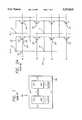
- a flash EEPROM 100commonly comprises a single substrate 102 in which one or more high density core regions 104 and a low density peripheral portion 106 are formed.
- High density core 104typically comprises at least one M ⁇ N array 104 of individually addressable, substantially identical memory cells 200 (FIGS. 2, 2A).
- Low density peripheral portion 106typically includes input/output (I/O) circuitry and circuitry for selectively addressing the individual cells.
- the selective addressing circuitrytypically includes one or more x-decoders and y-decoders, cooperating with the I/O circuitry for connecting the source, gate, and drain of selected addressed cells to predetermined voltages or impedances to effect designated operations on the cell, e.g., programming, reading and erasing, and deriving necessary voltages to effect such operations.
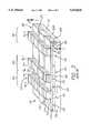
- each cell 200 in core 104typically comprises: source 202, drain 204, and channel 206 semiconductor regions formed in substrate 102 (or in a an isolation well); and a stacked gate (word line) structure 210.
- Gate structure 210suitably comprises: thin gate dielectric layer 212 (commonly referred to as the "tunnel oxide") formed on the surface of substrate 102 overlying channel 206; a floating gate 214 overlying tunnel oxide 212; an interpoly dielectric 216 overlying floating gate 214; and a control gate 218 overlying interpoly dielectric layer 216.
- Cells 200are arranged in a series of rows and columns.
- the control gates 218 of the respective cells 200 in a roware formed integral to a common word line (WL) associated with the row.
- Columns of cellsare arranged such that adjacent cells in a column share a common semiconductor region as source or drain regions:
- the source 202 of each cell in a column(excepting end cells) is formed in a common region with one of the adjacent cells, e.g., the preceding cell in the column;
- the drain of the cellis formed in a common region with the drain 204 of the other adjacent cell, e.g., next succeeding cell in the column.
- the drain of each cell in a column of cellsis connected by a conductive bit line (BL) (FIG.
- BLconductive bit line
- a pattern of field oxide regions 220is initially formed to provide electrical isolation between the respective devices of memory device 100.
- field oxide regionsare used to provide isolation between core array 104 and the devices of peripheral region 106, as well as between the various columns of cells 200 within core array 104.
- Field oxide regionsare conventionally formed using a mask and selective growth process: a layer of thermal oxide ("barrier oxide” or "pad oxide”) is grown or deposited over the surface of substrate 102; a mask, frequently composed of nitride, is deposited on the barrier oxide, and patterned to cover those regions of substrate 102 in which devices are to be formed (herein referred to as active regions); field oxide is grown in the exposed areas of the barrier oxide, by for example, local oxidation of silicon (LOCOS); and the masking layer and barrier oxide are stripped to expose the underlying substrate 102.
- LOCSlocal oxidation of silicon
- the selective growth processresults in alternating parallel strips of field oxide 220 and exposed regions corresponding to the columns of cells 200 in the array.
- Stacked gate-word line structures 210are then typically formed.
- tunnel dielectric 212suitably comprising a thin (e.g. approximately 100 angstroms) layer of oxide, is initially formed on substrate 102 by a suitable technique, such as, for example, thermally oxidizing the surface of substrate 102 or by depositing a suitable material on substrate 102.
- a layer of suitable conductive polysilicone.g., polycrystalline silicon
- conductive polysiliconmay be deposited by any suitable technique, e.g., conventional chemical vapor deposition (CVD).
- the polysilicon layeris typically then masked and etched to remove strips overlying field oxide regions 220, leaving isolated strips of polysilicon on top of tunnel dielectric 212 overlying the substrate regions corresponding to the columns of cells 200 of array 104 (i.e. the regions in which source, channel, and drain regions of cells in the column will be formed).
- a layer of suitable dielectric materialsuch as, e.g., an oxide-nitrate-oxide (ONO) layer, that will ultimately form interpoly dielectric 216 is typically then formed by a suitable technique.
- ONOoxide-nitrate-oxide
- Interpoly dielectric 216 layerin the completed array, insulates control gates 218 from floating gates 214 in the individual cells and electrically isolates the adjacent columns of floating gates 214 in array 104.
- Another layer of suitable conductive polysilicone.g., polycrystalline silicon
- control gates 218and word lines WL connecting the control gates of the cells in the respective rows of array 104
- a suitable techniquesuch as, for example, by conventional chemical vapor deposition (CVD).
- CVDchemical vapor deposition
- a silicide layermay be provided over polysilicon layer 218 to reduce resistance.
- Portions of the respective polysilicon and interpoly dielectric layersare typically then selectively removed, to define stacked gate structures 210 on tunnel dielectric layer 212, i.e., to form the floating gates 214, interpoly dielectric layer 216 and control gates 218 of the individual cells, and word lines WL (portions of interpoly dielectric 216 and control gate polysilicon layers, bridging field oxide regions 220, to connect the respective cells of the rows of the array).
- Thisis typically effected by suitable masking and etching techniques. When completed, this etch creates respective generally parallel word-line structures 210 separated by a distance D WL , as shown in FIG. 2.
- the portions of field oxide 220 and tunnel dielectric 212 between every second pair of adjacent word lines 210 in array 104are then typically removed, in preparation for formation of the common line (CS, FIG. 2) connecting the sources.
- Thisis typically effected using a conventional Self-Aligned Source (SAS) etch
- SASSelf-Aligned Source
- the selective etchtypically removes not only the exposed field oxide regions 220, but also the exposed tunnel oxide 212, a portion of the exposed polysilicon, and a portion of the underlying substrate 102.
- Source 202, common line CS, and drain 204 regionsare then formed.
- Source 202 and common source line CSare typically formed by initially effecting a conventional double diffusion implant (DDI), with the SAS mask still in place.
- the DDIimplants a first dopant (e.g. n-type), suitably phosphorous, to form a deeply diffused but lightly doped N well 202A (FIG. 2), establishing a graded source-channel junction.
- the SAS maskis then removed.
- the DDI implantis typically driven deeper into substrate 102, by subjecting substrate 102 to a thermal cycle at high temperature (e.g. 1050 degrees Celsius).
- a shallow second implantcommonly referred to as a medium diffused drain (MDD) implant, is then performed (e.g., with arsenic) to create a more heavily doped, but shallower, n+ well 202B embedded within deep N well 202A.
- the MDD implantalso forms a shallow, abrupt drain 204.
- periphery transistors, passivation layers, and conductive interconnect layersare then formed, the entire device is then oxidized to form a sealing layer of silicon dioxide (not shown) and finished and packaged for distribution.
- An individual cell 200is programmed by charging floating gate 214 through high energy electron injection, often referred to as hot electron injection.
- hot electronsare injected from channel 206 through tunnel dielectric 212 to negatively charge floating gate 214.
- Charging floating gate 214 with a negative potentialraises the threshold voltage of the cell by a predetermined amount V.sub. ⁇ from a first nominal value V T1 to a second nominal value V T2 .
- a programmed cell 200(V T >V T2 ) conducts substantially less current during a subsequent read operation than an unprogrammed cell 200 (V T ⁇ V T1 ) having no charge on floating gate 214.
- a predetermined voltage V Gis applied to control gate 218 of selected cell 200. If the selected cell 200 is unprogrammed (V T ⁇ V T1 ), the gate voltage V G exceeds the threshold voltage V T1 of the cell, and cell 200 conducts a relatively high current (above a predetermined upper threshold level, e.g. 100 microamps). Conduction of such high level current is indicative of a first state, e.g., a zero or logical low.
- gate voltage V Gis less than the threshold voltage V T2 of the cell, and the cell is non-conductive, or at least conducts less current (below a predetermined lower threshold level, e.g. 20 microamps). Conduction of such low level current is indicative of a second state, e.g., one or logical high.
- flash EEPROMsare typically bulk-erased, so that all of cells 200 in array 104 (i.e. connected to a common source line CS) are simultaneously erased.
- F-NFowler-Nordheim
- each cell 200is connected to common source line CS, all cells 200 in array 104 are erased for the same amount of time. Ideally, each cell 200 in array 104 requires the same amount of time to erase, i.e. to remove electrons from floating gate 214 and achieve a lower selected threshold voltage. Erase times among cells 200 within array 104, however, differ widely. Because of the variation in erase times, each cell 200 must be erased for the amount of time required to erase the slowest cell in array 104. Erasing faster cells 200 for too long, however, results in over-erasure. Over-erasure generates a positive charge on floating gate 214, which excessively lowers the threshold voltage V T of cell 200, in some instances to the extent of establishing a negative threshold voltage (V T ⁇ 0).
- the increased V.sub. ⁇ in threshold voltage effected by programmingmay not be sufficient to raise the threshold voltage V T of the over-erased cell above the predetermined voltage V G applied to control gate 218 of selected cell 200, so that even when programmed, the over-erased cell conducts upon application of V G during the read process, giving an erroneous reading.
- Column leakage currentmanifests itself by degrading or destroying the memory's reliability and endurance.
- the bit value of a selected cell 200depends on the magnitude of the drain current provided at the associated bit line BL. Drain 204 of each cell 200 in a column, however, is connected to the associated bit line BL.
- the only cell in the column biased for possible conductionis the cell in the selected word line WL; the predetermined voltage V G is applied to the gates of cells on the selected word line and all other gates are grounded during the reading process.
- bit lineIf selected cell 200 is unprogrammed, current in excess of the upper threshold value will be provided on the bit line, indicating e.g., a zero. If the selected cell is programmed with a "1", the drain current of the cell (and, ideally, the bit line), is below the lower threshold value during the read operation. However, the current in the bit line reflects the cumulative current flow from all of the cells in a column. Accordingly, if any of the cells in the column are over-erased and conduct significant current during the read operation, the current flow in the bit line may be in excess of the upper threshold value. Consequently, the read operation generates a logical zero regardless of which cell in the column is selected or whether the selected cell is programmed.
- a single over-erased celldisables the entire column.
- many of the cellsmay be slightly over-erased which provides a cumulative column leakage current in excess of the upper threshold value. For example, if each cell in a column of 512 cells leaks 0.2 microamps, the total column leakage current is 102.4 microamps, in excess of the upper threshold value of 100 microamps, thereby disabling the entire column.
- Milder casesmay simply degrade the performance of the memory over time, greatly reducing the reliability and endurance of the device, i.e. the number of cycles the device can be successfully programmed and erased.
- the disparity of erase times in conventional EEPROM cells 200 within array 104is caused, at least in part, by structural and doping variations among cells 200.
- the erase time of cell 200is affected by the F-N tunneling rate through tunnel dielectric 212, which, in turn, varies inversely with the square of the distance between floating gate 214 and source 202 in tunneling region 203 and varies directly with the doping concentration of tunneling region 203 near source 202, and specifically at the surface of channel 206.
- the geometry of each cell 200 near tunneling region 203is difficult to control without significantly increasing the size of each cell.
- a Self-Aligned Source (SAS) etchis typically used to remove the portions of field oxide 220 disposed between source regions 202 of the corresponding cells of adjacent rows (hereinafter referred to as the "inter-source” field oxide regions). Such an etch often causes variations in the geometries of the individual cells. Referring to FIGS.
- a masking layer of photo resist 302is deposited over array 104, then patterned to mask (cover) drain regions 204 and the field oxide regions 220 isolating the drains of cells in adjacent columns, with open strips 304 exposing the source regions 202 of the corresponding cells of adjacent rows and the inter-source portions of field oxide 220; openings 304 have edges 306 disposed along the centers of the word lines 210 of adjacent rows of cells.
- a highly selective etchis then performed to remove the exposed portions of field oxide 220.
- a conventional SAS etchis described in U.S. Pat. No. 5,120,671, issued Jun. 9, 1992, to Tang et al.
- the etchis highly selective in that it etches the field oxide at a much higher rate than the polysilicon word line or silicon, it is not totally selective; portions of the silicon of source region 202, as well as portions of the exposed polysilicon, are etched away. Referring to FIGS. 3 and 3A, the portions of tunnel dielectric 212 overlying the portions of substrate 102 where source regions 202 are to be formed are exposed by openings 304, as well as the inter-source portions of field oxide 220. The etch operates upon tunnel oxide 212 at the same rate as field oxide 220. Field oxide 220 is typically considerably thicker (e.g., 4000-5000 Angstroms) than tunnel oxide 212 (e.g., 100-200 Angstroms).
- the inter-source portions of field oxide 220are removed, not only has the etch removed the gate oxide 212 overlying the source region, but, as seen in FIG. 3A, it has also removed a portion of the silicon substrate 102 in the source region, producing a gouge of depth D G , typically of on the order of 200 Angstroms, in upper surface 308 of source region 202.
- the depth D G of the gouge in source region 202 and the profile of surface 308significantly affect the diffusion of dopants into tunneling region 203.
- the gougeincreases the distance through which the dopants must travel to extend to the surface of channel 206. Consequently, the gouge in surface 308 tends to decrease doping concentration in source 202 in tunneling region 203 when compared to an ungouged surface.
- the gougingvaries from cell to cell, creating non-uniformity.
- a portion 310 of the exposed area of word line 210is also etched away. This tends to create a longitudinal step of depth D G2 , typically on the order of 400 Angstroms, on the source side of the control gates 218 of the respective cells. This tends to increase the resistance of the word line.
- the etching processtypically does not produce a vertical edge where field oxide 220 is removed. Rather, the process tends to produce sloping edges 412, extending outwardly from the edge of word line 210. Sloping edges 412 tend to constrict the portion 414 of substrate 102 exposed for implantation in the vicinity of field oxide 220.
- the width of common source line CS connecting adjacent source regions 202tends to be less than the distance D WL between respective adjacent word lines (the length of the source regions), and the resistance of the common source line CS is increased as compared to a wider region. In conventional memory arrays, such resistance is in the range of from 150 to 1000 ohms per bit.
- the common source line CS of a memory array created using an SAS etching processmay present a 3 square resistance structure (length in direction of current flow to width ratio), equating to approximately 180 Ohms per bit.
- the present inventionprovides a mechanism avoiding the problems introduced by a self-aligned source etch process without sacrificing the advantages of self-aligned source technology. Rather than performing a self aligned source etch to remove the field oxide to facilitate forming the connection between adjacent source regions, a field oxide layer is left intact, and a high energy implantation process employed in conjunction with self aligned source mask to form the inter-source connection.
- FIG. 1is a top view of conventional memory device having an area of high density circuitry and an area of lower density circuitry;
- FIG. 2is a partial, sectional perspective of a portion of an intermediate state (partially complete) of a cell array core 104;
- FIG. 2Ais a schematic diagram of a portion of the cell array
- FIG. 3is a partial, sectional view of an intermediate state (partially complete) of a portion of a cell array taken along section A--A in FIG. 3B, showing respective adjacent word lines and a self aligned source masking layer prior to a selective etching;
- FIG. 3Ais a partial, sectional view of an intermediate state (partially complete) of a portion of a cell array taken along section A--A in FIG. 3B, showing respective adjacent word lines and a self aligned source masking layer after a selective etching;
- FIG. 3Bis a partial, top view of an intermediate state (partially complete) of a portion of a conventional cell array showing respective adjacent word lines, field oxide, and source and drain regions, after a conventional self aligned source etching process;
- FIG. 4is a partial, sectional view of an intermediate state (partially complete) of a portion of a cell array taken along section B--B in FIG. 3B, showing respective adjacent word lines and a self aligned source masking layer prior to a selective etching;
- FIG. 4Ais a partial, sectional view of an intermediate state (partially complete) of a portion of a cell array taken along section B--B in FIG. 3B, showing respective adjacent word lines and a self aligned source masking layer after a selective etching;
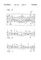
- FIG. 5is a partial, sectional view of an intermediate state (partially complete) of a portion of a cell array, taken along section C--C in FIG. 2, illustrating implantation of a source interconnect region in accordance with the present invention
- FIG. 6is a partial, sectional view of an intermediate state (partially complete) of a portion of a cell array, taken along section C--C in FIG. 2, illustrating overly deep implantation of a source interconnect region;
- FIG. 7is a partial, sectional view of an intermediate state (partially complete) of a portion of a cell array, taken along section C--C in FIG. 2, illustrating a two energy implantation of a source interconnect region in accordance with the present invention
- FIG. 8is a flowchart of a formation process employing implantation of a source interconnect region in accordance with the present invention.
- FIG. 9is a flowchart of a an alternative formation process employing implantation of a source interconnect region in accordance with the present invention.
- a pattern of field oxide regions 220is initially formed on a suitable substrate 102 (e.g., silicon doped with p-type dopants, such as boron). Field oxide regions 220 are patterned to form strips interposed between the areas where columns of cells will be formed. A series of parallel stacked gate-word line structures 210 (one corresponding to each row) are then formed, perpendicular to and extending over field oxide strips 220, spaced apart by distance D WL . The criss-crossing pattern of field oxide strips 220 and stacked gateword line structure may be formed by any suitable methodology.
- a self-aligned source etchis performed to remove the inter-source portions of field oxide 220, followed by further doping in exposed regions of substrate 102 (in predetermined disposition to stacked gate structures 210) to form the source and drain regions of cells 200.
- the inter-source connectionsare effected without performing a self aligned source etch to remove the inner-source field oxide regions by implanting a sufficiently high dose of dopants at a sufficiently high energy level to form low resistivity source interconnection regions underlying field oxide regions 220, electrically connecting adjacent source regions.
- a self aligned source etchto remove the inner-source field oxide regions by implanting a sufficiently high dose of dopants at a sufficiently high energy level to form low resistivity source interconnection regions underlying field oxide regions 220, electrically connecting adjacent source regions.
- the implantationcan be effected by any suitable method.
- implantationinvolves ionizing a gaseous form of the dopant, and subjecting the ions to a high level electric field.
- the electrical fieldaccelerates the ions to cause them to penetrate into the wafer to a depth corresponding to the strength of the electric field.
- Implantationis effected at an energy level sufficient to cause the dopant to pass through the inter-source field oxide regions and locate within a predetermined region in substrate 102 to effect an electrical connection between the corresponding source regions of adjacent columns.
- a self-aligned source mask 302is formed and patterned in a conventional manner to expose source regions 202 and inter-source portions of field oxide 220.
- a high energy implantation stepis then effected on the exposed source regions 202 and inter-source field oxide 220 portions to implant a relatively low resistivity region 500 in substrate 102, underlying field oxide 220 and in contact with source regions 202.
- the dopant doseis chosen to ensure a relatively low resistance, of, for example, from 20 to 40 ohms per bit (as compared to 150 to 1,000 ohms per bit in conventional structures) to provide such low resistivity, the dose is typically in the range of 2.5 ⁇ 10 14 to 1 ⁇ 10 16 ions/cm 2 preferably, the implantation provides a 0.75 square resistance structure (equating to approximately 45 ohms per bit) as compared to a 3 square resistance structure (equating to approximately 180 ohms per bit) in conventional structures.
- the implantation energy levelshould be sufficient to drive the dopants through inter-source field oxide portions 220 and into substrate 102.
- the energy level at which the implantation is effectedis a function of the particular species of dopant employed, and the desired depth of the interconnect region 500, chosen to ensure electrical connection with source regions 202.
- dopants employedare chosen to provide good conductivity, e.g., Arsenic (AS), Phosphorus (P) and Antimony (SB).
- ASArsenic
- PPhosphorus
- SBAntimony
- the thickness D OF of field oxide regions 220are generally in the range of 400 to 5,000 angstroms, whereas the source region generally extends a distance D S into the substrate in the range of 200 to 3,000 angstroms.
- Typical energy levels for various dopants sufficient to cause the dopant to pass through field oxide 220 and to form inter-connect region 500 in substrate 102 to make electrical connection with source region 202are shown in TABLE I.
- dopantstravel comparable distances through field oxide and silicon. Accordingly, referring to FIG. 6, in some instances, particularly those where field oxide 220 extends further into substrate 102 than does source region 202, use of energy levels sufficient to implant interconnecting region 500 in substrate 102 through field oxide 220, may dispose inter-connect region 500 below, and out of contact with, source region 202, spaced apart from source 202 by an intervening portion 600 of substrate 102. In some instances, subjecting the device to a heat cycle to diffuse the dopants can effect contact between source regions 202 and inter-connect region 500. However, the thermal cycle tends to extend the width of the source connection region and excessive thermal cycle can interfere with the memory cell read and program operations.
- a second implantation at a lower energy level designed to implant dopants in intervening region 600can be employed to effect electrical connection between inter-connect region 500 and sources 202.
- supplemental implantationeffected at a lower energy level, is employed to implant dopants in region 600, effectively extending inner connect region 500 into electrical connection with source regions 202.
- different speciescan be implanted at the same or different energy levels to ensure the connection.
- a pattern of field oxide regions 220 (Step 800) and gate/word line structures 210 (Step 802)are initially formed by any suitable techniques.
- the control gate 218 of word-lines 210is suitably formed with a tungsten silicide film sandwiched between two polysilicon layers; The tungsten silicide reduces the resistance of gate 218, and also provides additional protection for the channel region during the high energy implantation.
- the source 202 and drain 204 regionsare then formed in substrate 102 (Steps 804). Source and drain regions may be formed by any suitable procedure.
- a self aligned source maskis formed to mask off the drain regions and inter-drain field oxide regions (Step 806); a conventional double diffusion implant (DDI) is effected with the mask in place (Step 808); a thermal cycle is performed (step 809); the mask is removed (Step 810); a medium defused implant (MDD) is effected (Step 812); then, a thermal cycle is effected at high temperature (e.g. 1050 degrees C.) to defuse the dopants (Step 818)
- DDDdouble diffusion implant
- MDDmedium defused implant
- the devices in peripheral region 106are then formed, by any suitable processes (Step 820) and a thermal cycle effected (typicly part of the peripheral device formation) (Step 822).
- Step 824After the peripheral devices have been formed, and any attendant thermal cycles effected, the source interconnection is made (Steps 824).
- An SAS mask similar to that used in connection with doping the source regionsis formed (Step 826).
- a high energy implantis then effected to create interconnect region 500 (FIG. 5) (Step 828). If necessary, or desirable, a second lower energy implantation can be performed to ensure electrical connection between sources 202 and interconnect region 500.
- Array 104 and EEPROM 100are then completed by any suitable process (step 830).
- suitable processfor example, conventional techniques are thereafter suitably employed to form passivation layers, and conductive interconnect layers (formed of, for example, polysilicon or metal), wafer oxidation and packaging.
- the point in the overall fabrication process at which the source interconnect implantation is effectedis typically a function of a number of high temperature processes employed in the overall fabrication process, and the desired amount of diffusion.
- the source interconnect implantation(Steps 824) can be effected earlier in the overall fabrication process.
- the source interconnect implantation(Steps 824) can be effected prior to formation of peripheral devices (Step 820) so that interconnect region 500 is subjected to the attendant thermal cycles (Step 822).
- the source connect regioncan extend the entire width of the space between word-lines D WL , and is not subject to the constriction created by field oxide 220 in prior art processes. Accordingly, the resistance of the interconnect is considerably less than in the prior art (e.g., 0.75 square, as compared to 3 square). In addition, nonuniformities, and concomitant effect on V T distribution caused by the etching process is avoided.
Landscapes
- Semiconductor Memories (AREA)
- Non-Volatile Memory (AREA)
Abstract
Description
TABLE I ______________________________________ DOPANT ENERGY ______________________________________ Arsenic 70 Kev-3 Mev Phosphorous 35 Kev-700 Kev Antimony 90 Kev-5 Mev ______________________________________
Claims (4)
Priority Applications (2)
| Application Number | Priority Date | Filing Date | Title |
|---|---|---|---|
| US08/484,580US5553018A (en) | 1995-06-07 | 1995-06-07 | Nonvolatile memory cell formed using self aligned source implant |
| US08/474,879US5656513A (en) | 1995-06-07 | 1995-06-07 | Nonvolatile memory cell formed using self aligned source implant |
Applications Claiming Priority (1)
| Application Number | Priority Date | Filing Date | Title |
|---|---|---|---|
| US08/484,580US5553018A (en) | 1995-06-07 | 1995-06-07 | Nonvolatile memory cell formed using self aligned source implant |
Related Child Applications (1)
| Application Number | Title | Priority Date | Filing Date |
|---|---|---|---|
| US08/474,879DivisionUS5656513A (en) | 1995-06-07 | 1995-06-07 | Nonvolatile memory cell formed using self aligned source implant |
Publications (1)
| Publication Number | Publication Date |
|---|---|
| US5553018Atrue US5553018A (en) | 1996-09-03 |
Family
ID=23924736
Family Applications (2)
| Application Number | Title | Priority Date | Filing Date |
|---|---|---|---|
| US08/474,879Expired - LifetimeUS5656513A (en) | 1995-06-07 | 1995-06-07 | Nonvolatile memory cell formed using self aligned source implant |
| US08/484,580Expired - LifetimeUS5553018A (en) | 1995-06-07 | 1995-06-07 | Nonvolatile memory cell formed using self aligned source implant |
Family Applications Before (1)
| Application Number | Title | Priority Date | Filing Date |
|---|---|---|---|
| US08/474,879Expired - LifetimeUS5656513A (en) | 1995-06-07 | 1995-06-07 | Nonvolatile memory cell formed using self aligned source implant |
Country Status (1)
| Country | Link |
|---|---|
| US (2) | US5656513A (en) |
Cited By (64)
| Publication number | Priority date | Publication date | Assignee | Title |
|---|---|---|---|---|
| FR2753004A1 (en)* | 1996-09-04 | 1998-03-06 | Oki Electric Ind Co Ltd | NON-VOLATILE SEMICONDUCTOR MEMORY AND METHOD OF MANUFACTURING SAME |
| US5726470A (en)* | 1995-02-28 | 1998-03-10 | Nippon Steel Corporation | Nonvolatile semiconductor memory device and method of fabrication of the same |
| US5854108A (en)* | 1996-06-04 | 1998-12-29 | Advanced Micro Devices, Inc. | Method and system for providing a double diffuse implant junction in a flash device |
| US5972749A (en)* | 1998-01-05 | 1999-10-26 | Advanced Micro Devices, Inc. | Method for preventing P1 punchthrough |
| US6133095A (en)* | 1999-02-04 | 2000-10-17 | Saifun Semiconductors Ltd. | Method for creating diffusion areas for sources and drains without an etch step |
| US6136649A (en)* | 1999-10-12 | 2000-10-24 | Advanced Micro Devices, Inc. | Method for removing anti-reflective coating layer using plasma etch process after contact CMP |
| US6242773B1 (en)* | 1998-09-30 | 2001-06-05 | Advanced Micro Devices, Inc. | Self-aligning poly 1 ono dielectric for non-volatile memory |
| US6281544B1 (en)* | 1998-08-04 | 2001-08-28 | United Microelectronics, Corp. | Flash memory structure and method of manufacture |
| US6288423B1 (en)* | 1997-04-18 | 2001-09-11 | Nippon Steel Corporation | Composite gate structure memory cell having increased capacitance |
| US6291296B1 (en) | 1999-10-12 | 2001-09-18 | Advanced Micro Devices, Inc. | Method for removing anti-reflective coating layer using plasma etch process before contact CMP |
| US6348379B1 (en) | 2000-02-11 | 2002-02-19 | Advanced Micro Devices, Inc. | Method of forming self-aligned contacts using consumable spacers |
| US6359307B1 (en)* | 2000-01-29 | 2002-03-19 | Advanced Micro Devices, Inc. | Method for forming self-aligned contacts and interconnection lines using dual damascene techniques |
| US6392267B1 (en) | 1997-04-25 | 2002-05-21 | Alliance Semiconductor Corporation | Flash EPROM array with self-aligned source contacts and programmable sector erase architecture |
| US6410390B1 (en) | 2000-02-03 | 2002-06-25 | Hyundai Electronics Industries Co., Ltd. | Nonvolatile memory device and method for fabricating the same |
| US6420752B1 (en) | 2000-02-11 | 2002-07-16 | Advanced Micro Devices, Inc. | Semiconductor device with self-aligned contacts using a liner oxide layer |
| US6429063B1 (en) | 1999-10-26 | 2002-08-06 | Saifun Semiconductors Ltd. | NROM cell with generally decoupled primary and secondary injection |
| US6430077B1 (en) | 1997-12-12 | 2002-08-06 | Saifun Semiconductors Ltd. | Method for regulating read voltage level at the drain of a cell in a symmetric array |
| US6477084B2 (en) | 1998-05-20 | 2002-11-05 | Saifun Semiconductors Ltd. | NROM cell with improved programming, erasing and cycling |
| US6490204B2 (en) | 2000-05-04 | 2002-12-03 | Saifun Semiconductors Ltd. | Programming and erasing methods for a reference cell of an NROM array |
| US6548334B1 (en)* | 1999-09-27 | 2003-04-15 | Advanced Micro Devices, Inc. | Capping layer |
| US6552387B1 (en) | 1997-07-30 | 2003-04-22 | Saifun Semiconductors Ltd. | Non-volatile electrically erasable and programmable semiconductor memory cell utilizing asymmetrical charge trapping |
| US6584017B2 (en) | 2001-04-05 | 2003-06-24 | Saifun Semiconductors Ltd. | Method for programming a reference cell |
| US6583007B1 (en) | 2001-12-20 | 2003-06-24 | Saifun Semiconductors Ltd. | Reducing secondary injection effects |
| US6583465B1 (en)* | 1999-12-28 | 2003-06-24 | Hyundai Electronics Industries Co., Ltd | Code addressable memory cell in a flash memory device |
| US20030117861A1 (en)* | 2001-12-20 | 2003-06-26 | Eduardo Maayan | NROM NOR array |
| US6586806B1 (en)* | 1997-06-20 | 2003-07-01 | Cypress Semiconductor Corporation | Method and structure for a single-sided non-self-aligned transistor |
| US20030142544A1 (en)* | 2002-01-31 | 2003-07-31 | Eduardo Maayan | Mass storage array and methods for operation thereof |
| US6614692B2 (en) | 2001-01-18 | 2003-09-02 | Saifun Semiconductors Ltd. | EEPROM array and method for operation thereof |
| US6633499B1 (en) | 1997-12-12 | 2003-10-14 | Saifun Semiconductors Ltd. | Method for reducing voltage drops in symmetric array architectures |
| US6633496B2 (en) | 1997-12-12 | 2003-10-14 | Saifun Semiconductors Ltd. | Symmetric architecture for memory cells having widely spread metal bit lines |
| US6636440B2 (en) | 2001-04-25 | 2003-10-21 | Saifun Semiconductors Ltd. | Method for operation of an EEPROM array, including refresh thereof |
| US6643181B2 (en) | 2001-10-24 | 2003-11-04 | Saifun Semiconductors Ltd. | Method for erasing a memory cell |
| US6649972B2 (en) | 1997-08-01 | 2003-11-18 | Saifun Semiconductors Ltd. | Two bit non-volatile electrically erasable and programmable semiconductor memory cell utilizing asymmetrical charge trapping |
| US6664588B2 (en) | 1998-05-20 | 2003-12-16 | Saifun Semiconductors Ltd. | NROM cell with self-aligned programming and erasure areas |
| US6677805B2 (en) | 2001-04-05 | 2004-01-13 | Saifun Semiconductors Ltd. | Charge pump stage with body effect minimization |
| US20040008541A1 (en)* | 2002-07-10 | 2004-01-15 | Eduardo Maayan | Multiple use memory chip |
| US6774426B2 (en)* | 2000-12-19 | 2004-08-10 | Micron Technology, Inc. | Flash cell with trench source-line connection |
| US6800894B1 (en)* | 1998-12-11 | 2004-10-05 | Seiko Epson Corporation | Semiconductor devices, circuit substrates and electronic devices |
| US6826107B2 (en) | 2002-08-01 | 2004-11-30 | Saifun Semiconductors Ltd. | High voltage insertion in flash memory cards |
| US6828625B2 (en) | 2001-11-19 | 2004-12-07 | Saifun Semiconductors Ltd. | Protective layer in memory device and method therefor |
| US6829172B2 (en) | 2000-05-04 | 2004-12-07 | Saifun Semiconductors Ltd. | Programming of nonvolatile memory cells |
| US6928001B2 (en) | 2000-12-07 | 2005-08-09 | Saifun Semiconductors Ltd. | Programming and erasing methods for a non-volatile memory cell |
| US7221138B2 (en) | 2005-09-27 | 2007-05-22 | Saifun Semiconductors Ltd | Method and apparatus for measuring charge pump output current |
| US7317633B2 (en) | 2004-07-06 | 2008-01-08 | Saifun Semiconductors Ltd | Protection of NROM devices from charge damage |
| US7352627B2 (en) | 2006-01-03 | 2008-04-01 | Saifon Semiconductors Ltd. | Method, system, and circuit for operating a non-volatile memory array |
| US7369440B2 (en) | 2005-01-19 | 2008-05-06 | Saifun Semiconductors Ltd. | Method, circuit and systems for erasing one or more non-volatile memory cells |
| US7420848B2 (en) | 2002-01-31 | 2008-09-02 | Saifun Semiconductors Ltd. | Method, system, and circuit for operating a non-volatile memory array |
| US7457183B2 (en) | 2003-09-16 | 2008-11-25 | Saifun Semiconductors Ltd. | Operating array cells with matched reference cells |
| US7466594B2 (en) | 2004-08-12 | 2008-12-16 | Saifun Semiconductors Ltd. | Dynamic matching of signal path and reference path for sensing |
| US7532529B2 (en) | 2004-03-29 | 2009-05-12 | Saifun Semiconductors Ltd. | Apparatus and methods for multi-level sensing in a memory array |
| US7535765B2 (en) | 2004-12-09 | 2009-05-19 | Saifun Semiconductors Ltd. | Non-volatile memory device and method for reading cells |
| US7605579B2 (en) | 2006-09-18 | 2009-10-20 | Saifun Semiconductors Ltd. | Measuring and controlling current consumption and output current of charge pumps |
| US7638850B2 (en) | 2004-10-14 | 2009-12-29 | Saifun Semiconductors Ltd. | Non-volatile memory structure and method of fabrication |
| US7638835B2 (en) | 2006-02-28 | 2009-12-29 | Saifun Semiconductors Ltd. | Double density NROM with nitride strips (DDNS) |
| US7668017B2 (en) | 2005-08-17 | 2010-02-23 | Saifun Semiconductors Ltd. | Method of erasing non-volatile memory cells |
| US7675782B2 (en) | 2002-10-29 | 2010-03-09 | Saifun Semiconductors Ltd. | Method, system and circuit for programming a non-volatile memory array |
| US7692961B2 (en) | 2006-02-21 | 2010-04-06 | Saifun Semiconductors Ltd. | Method, circuit and device for disturb-control of programming nonvolatile memory cells by hot-hole injection (HHI) and by channel hot-electron (CHE) injection |
| US7701779B2 (en) | 2006-04-27 | 2010-04-20 | Sajfun Semiconductors Ltd. | Method for programming a reference cell |
| US7743230B2 (en) | 2003-01-31 | 2010-06-22 | Saifun Semiconductors Ltd. | Memory array programming circuit and a method for using the circuit |
| US7760554B2 (en) | 2006-02-21 | 2010-07-20 | Saifun Semiconductors Ltd. | NROM non-volatile memory and mode of operation |
| US7786512B2 (en) | 2005-07-18 | 2010-08-31 | Saifun Semiconductors Ltd. | Dense non-volatile memory array and method of fabrication |
| US7808818B2 (en) | 2006-01-12 | 2010-10-05 | Saifun Semiconductors Ltd. | Secondary injection for NROM |
| US8053812B2 (en) | 2005-03-17 | 2011-11-08 | Spansion Israel Ltd | Contact in planar NROM technology |
| US8253452B2 (en) | 2006-02-21 | 2012-08-28 | Spansion Israel Ltd | Circuit and method for powering up an integrated circuit and an integrated circuit utilizing same |
Families Citing this family (12)
| Publication number | Priority date | Publication date | Assignee | Title |
|---|---|---|---|---|
| JP3461998B2 (en)* | 1995-03-24 | 2003-10-27 | セイコーインスツルメンツ株式会社 | Electrically rewritable semiconductor nonvolatile memory device and method of manufacturing the same |
| KR100198624B1 (en)* | 1995-12-20 | 1999-06-15 | 구본준 | Fabricating method of semiconductor device |
| US5933730A (en)* | 1997-03-07 | 1999-08-03 | Advanced Micro Devices, Inc. | Method of spacer formation and source protection after self-aligned source is formed and a device provided by such a method |
| JP2000022114A (en)* | 1998-07-02 | 2000-01-21 | Rohm Co Ltd | Semiconductor storage device and its manufacture |
| US6133097A (en)* | 1998-08-14 | 2000-10-17 | Taiwan Semiconductor Manufacturing Company | Method for forming mirror image split gate flash memory devices by forming a central source line slot |
| US6251717B1 (en) | 1998-09-30 | 2001-06-26 | Advanced Micro Devices, Inc. | Viable memory cell formed using rapid thermal annealing |
| US6465835B1 (en) | 1999-09-27 | 2002-10-15 | Advanced Micro Devices, Inc. | Charge gain/charge loss junction leakage prevention for flash technology by using double isolation/capping layer between lightly doped drain and gate |
| US6654283B1 (en) | 2001-12-11 | 2003-11-25 | Advanced Micro Devices Inc. | Flash memory array architecture and method of programming, erasing and reading thereof |
| US6737703B1 (en)* | 2002-03-12 | 2004-05-18 | Advanced Micro Devices, Inc. | Memory array with buried bit lines |
| US6646914B1 (en) | 2002-03-12 | 2003-11-11 | Advanced Micro Devices, Inc. | Flash memory array architecture having staggered metal lines |
| US6754109B1 (en) | 2002-10-29 | 2004-06-22 | Advanced Micro Devices, Inc. | Method of programming memory cells |
| US7074682B2 (en)* | 2003-10-01 | 2006-07-11 | Dongbuanam Semiconductor Inc. | Method for fabricating a semiconductor device having self aligned source (SAS) crossing trench |
Citations (3)
| Publication number | Priority date | Publication date | Assignee | Title |
|---|---|---|---|---|
| US4500899A (en)* | 1980-12-25 | 1985-02-19 | Fujitsu Limited | Semiconductor memory device and process for producing the same |
| US5103274A (en)* | 1990-11-29 | 1992-04-07 | Intel Corporation | Self-aligned source process and apparatus |
| US5394001A (en)* | 1992-05-26 | 1995-02-28 | Kabushiki Kaisha Toshiba | Nonvolatile semiconductor memory device having reduced resistance value for the common source wiring region |
Family Cites Families (7)
| Publication number | Priority date | Publication date | Assignee | Title |
|---|---|---|---|---|
| US5087584A (en)* | 1990-04-30 | 1992-02-11 | Intel Corporation | Process for fabricating a contactless floating gate memory array utilizing wordline trench vias |
| US5151375A (en)* | 1990-06-13 | 1992-09-29 | Waferscale Integration, Inc. | EPROM virtual ground array |
| US5120671A (en)* | 1990-11-29 | 1992-06-09 | Intel Corporation | Process for self aligning a source region with a field oxide region and a polysilicon gate |
| US5297082A (en)* | 1992-11-12 | 1994-03-22 | Micron Semiconductor, Inc. | Shallow trench source eprom cell |
| US5384268A (en)* | 1993-01-22 | 1995-01-24 | United Microelectronics Corporation | Charge damage free implantation by introduction of a thin conductive layer |
| US5335198A (en)* | 1993-05-06 | 1994-08-02 | Advanced Micro Devices, Inc. | Flash EEPROM array with high endurance |
| US5482881A (en)* | 1995-03-14 | 1996-01-09 | Advanced Micro Devices, Inc. | Method of making flash EEPROM memory with reduced column leakage current |
- 1995
- 1995-06-07USUS08/474,879patent/US5656513A/ennot_activeExpired - Lifetime
- 1995-06-07USUS08/484,580patent/US5553018A/ennot_activeExpired - Lifetime
Patent Citations (3)
| Publication number | Priority date | Publication date | Assignee | Title |
|---|---|---|---|---|
| US4500899A (en)* | 1980-12-25 | 1985-02-19 | Fujitsu Limited | Semiconductor memory device and process for producing the same |
| US5103274A (en)* | 1990-11-29 | 1992-04-07 | Intel Corporation | Self-aligned source process and apparatus |
| US5394001A (en)* | 1992-05-26 | 1995-02-28 | Kabushiki Kaisha Toshiba | Nonvolatile semiconductor memory device having reduced resistance value for the common source wiring region |
Cited By (91)
| Publication number | Priority date | Publication date | Assignee | Title |
|---|---|---|---|---|
| US5726470A (en)* | 1995-02-28 | 1998-03-10 | Nippon Steel Corporation | Nonvolatile semiconductor memory device and method of fabrication of the same |
| US5960283A (en)* | 1995-02-28 | 1999-09-28 | Nippon Steel Corporation | Nonvolatile semiconductor memory device and method of fabrication of the same |
| US5854108A (en)* | 1996-06-04 | 1998-12-29 | Advanced Micro Devices, Inc. | Method and system for providing a double diffuse implant junction in a flash device |
| US5966602A (en)* | 1996-09-04 | 1999-10-12 | Oki Electric Industry Co., Ltd. | Nonvolatile semiconductor memory and fabricating method thereof |
| FR2753004A1 (en)* | 1996-09-04 | 1998-03-06 | Oki Electric Ind Co Ltd | NON-VOLATILE SEMICONDUCTOR MEMORY AND METHOD OF MANUFACTURING SAME |
| USRE42004E1 (en) | 1997-04-18 | 2010-12-21 | Fumitaka Sugaya | Method for fabricating a semiconductor storage device having an increased dielectric film area |
| US6288423B1 (en)* | 1997-04-18 | 2001-09-11 | Nippon Steel Corporation | Composite gate structure memory cell having increased capacitance |
| US6392267B1 (en) | 1997-04-25 | 2002-05-21 | Alliance Semiconductor Corporation | Flash EPROM array with self-aligned source contacts and programmable sector erase architecture |
| US6586806B1 (en)* | 1997-06-20 | 2003-07-01 | Cypress Semiconductor Corporation | Method and structure for a single-sided non-self-aligned transistor |
| US6566699B2 (en) | 1997-07-30 | 2003-05-20 | Saifun Semiconductors Ltd. | Non-volatile electrically erasable and programmable semiconductor memory cell utilizing asymmetrical charge trapping |
| US6552387B1 (en) | 1997-07-30 | 2003-04-22 | Saifun Semiconductors Ltd. | Non-volatile electrically erasable and programmable semiconductor memory cell utilizing asymmetrical charge trapping |
| US6803299B2 (en) | 1997-07-30 | 2004-10-12 | Saifun Semiconductors Ltd. | Non-volatile electrically erasable and programmable semiconductor memory cell utilizing asymmetrical charge trapping |
| US6768165B1 (en) | 1997-08-01 | 2004-07-27 | Saifun Semiconductors Ltd. | Two bit non-volatile electrically erasable and programmable semiconductor memory cell utilizing asymmetrical charge trapping |
| US7116577B2 (en) | 1997-08-01 | 2006-10-03 | Saifun Semiconductors Ltd | Two bit non-volatile electrically erasable and programmable semiconductor memory cell utilizing asymmetrical charge trapping |
| US7405969B2 (en) | 1997-08-01 | 2008-07-29 | Saifun Semiconductors Ltd. | Non-volatile memory cell and non-volatile memory devices |
| US6649972B2 (en) | 1997-08-01 | 2003-11-18 | Saifun Semiconductors Ltd. | Two bit non-volatile electrically erasable and programmable semiconductor memory cell utilizing asymmetrical charge trapping |
| US6633499B1 (en) | 1997-12-12 | 2003-10-14 | Saifun Semiconductors Ltd. | Method for reducing voltage drops in symmetric array architectures |
| US6633496B2 (en) | 1997-12-12 | 2003-10-14 | Saifun Semiconductors Ltd. | Symmetric architecture for memory cells having widely spread metal bit lines |
| US6430077B1 (en) | 1997-12-12 | 2002-08-06 | Saifun Semiconductors Ltd. | Method for regulating read voltage level at the drain of a cell in a symmetric array |
| US6066873A (en)* | 1998-01-05 | 2000-05-23 | Advanced Micro Devices, Inc. | Method and apparatus for preventing P1 punchthrough |
| US5972749A (en)* | 1998-01-05 | 1999-10-26 | Advanced Micro Devices, Inc. | Method for preventing P1 punchthrough |
| US6477084B2 (en) | 1998-05-20 | 2002-11-05 | Saifun Semiconductors Ltd. | NROM cell with improved programming, erasing and cycling |
| US6664588B2 (en) | 1998-05-20 | 2003-12-16 | Saifun Semiconductors Ltd. | NROM cell with self-aligned programming and erasure areas |
| US6281544B1 (en)* | 1998-08-04 | 2001-08-28 | United Microelectronics, Corp. | Flash memory structure and method of manufacture |
| US6242773B1 (en)* | 1998-09-30 | 2001-06-05 | Advanced Micro Devices, Inc. | Self-aligning poly 1 ono dielectric for non-volatile memory |
| US6800894B1 (en)* | 1998-12-11 | 2004-10-05 | Seiko Epson Corporation | Semiconductor devices, circuit substrates and electronic devices |
| US7163861B2 (en) | 1998-12-11 | 2007-01-16 | Seiko Epson Corporation | Semiconductor devices, methods of manufacturing semiconductor devices, circuit substrates and electronic devices |
| US20050003615A1 (en)* | 1998-12-11 | 2005-01-06 | Tomoyuki Furuhata | Semiconductor devices, methods of manufacturing semiconductor devices, circuit substrates and electronic devices |
| US6133095A (en)* | 1999-02-04 | 2000-10-17 | Saifun Semiconductors Ltd. | Method for creating diffusion areas for sources and drains without an etch step |
| US6548334B1 (en)* | 1999-09-27 | 2003-04-15 | Advanced Micro Devices, Inc. | Capping layer |
| US6136649A (en)* | 1999-10-12 | 2000-10-24 | Advanced Micro Devices, Inc. | Method for removing anti-reflective coating layer using plasma etch process after contact CMP |
| US6291296B1 (en) | 1999-10-12 | 2001-09-18 | Advanced Micro Devices, Inc. | Method for removing anti-reflective coating layer using plasma etch process before contact CMP |
| US6429063B1 (en) | 1999-10-26 | 2002-08-06 | Saifun Semiconductors Ltd. | NROM cell with generally decoupled primary and secondary injection |
| US6583465B1 (en)* | 1999-12-28 | 2003-06-24 | Hyundai Electronics Industries Co., Ltd | Code addressable memory cell in a flash memory device |
| US6359307B1 (en)* | 2000-01-29 | 2002-03-19 | Advanced Micro Devices, Inc. | Method for forming self-aligned contacts and interconnection lines using dual damascene techniques |
| US6410390B1 (en) | 2000-02-03 | 2002-06-25 | Hyundai Electronics Industries Co., Ltd. | Nonvolatile memory device and method for fabricating the same |
| US6677638B2 (en) | 2000-02-03 | 2004-01-13 | Hyundai Electronics Industries Co., Ltd. | Nonvolatile memory device and method for fabricating the same |
| US6420752B1 (en) | 2000-02-11 | 2002-07-16 | Advanced Micro Devices, Inc. | Semiconductor device with self-aligned contacts using a liner oxide layer |
| US6348379B1 (en) | 2000-02-11 | 2002-02-19 | Advanced Micro Devices, Inc. | Method of forming self-aligned contacts using consumable spacers |
| US6490204B2 (en) | 2000-05-04 | 2002-12-03 | Saifun Semiconductors Ltd. | Programming and erasing methods for a reference cell of an NROM array |
| US6937521B2 (en) | 2000-05-04 | 2005-08-30 | Saifun Semiconductors Ltd. | Programming and erasing methods for a non-volatile memory cell |
| US6829172B2 (en) | 2000-05-04 | 2004-12-07 | Saifun Semiconductors Ltd. | Programming of nonvolatile memory cells |
| US6928001B2 (en) | 2000-12-07 | 2005-08-09 | Saifun Semiconductors Ltd. | Programming and erasing methods for a non-volatile memory cell |
| US6774426B2 (en)* | 2000-12-19 | 2004-08-10 | Micron Technology, Inc. | Flash cell with trench source-line connection |
| US6949791B2 (en) | 2000-12-19 | 2005-09-27 | Micron Technology, Inc. | Flash cell with trench source-line connection |
| US20040262671A1 (en)* | 2000-12-19 | 2004-12-30 | Micron Technology, Inc. | Flash cell with trench source-line connection |
| US7518908B2 (en) | 2001-01-18 | 2009-04-14 | Saifun Semiconductors Ltd. | EEPROM array and method for operation thereof |
| US6614692B2 (en) | 2001-01-18 | 2003-09-02 | Saifun Semiconductors Ltd. | EEPROM array and method for operation thereof |
| US7064983B2 (en) | 2001-04-05 | 2006-06-20 | Saifum Semiconductors Ltd. | Method for programming a reference cell |
| US6584017B2 (en) | 2001-04-05 | 2003-06-24 | Saifun Semiconductors Ltd. | Method for programming a reference cell |
| US6677805B2 (en) | 2001-04-05 | 2004-01-13 | Saifun Semiconductors Ltd. | Charge pump stage with body effect minimization |
| US6864739B2 (en) | 2001-04-05 | 2005-03-08 | Saifun Semiconductors Ltd. | Charge pump stage with body effect minimization |
| US20040130385A1 (en)* | 2001-04-05 | 2004-07-08 | Shor Joseph S. | Charge pump stage with body effect minimization |
| US6636440B2 (en) | 2001-04-25 | 2003-10-21 | Saifun Semiconductors Ltd. | Method for operation of an EEPROM array, including refresh thereof |
| US6643181B2 (en) | 2001-10-24 | 2003-11-04 | Saifun Semiconductors Ltd. | Method for erasing a memory cell |
| US6888757B2 (en) | 2001-10-24 | 2005-05-03 | Saifun Semiconductors Ltd. | Method for erasing a memory cell |
| US6828625B2 (en) | 2001-11-19 | 2004-12-07 | Saifun Semiconductors Ltd. | Protective layer in memory device and method therefor |
| US7098107B2 (en) | 2001-11-19 | 2006-08-29 | Saifun Semiconductor Ltd. | Protective layer in memory device and method therefor |
| US6583007B1 (en) | 2001-12-20 | 2003-06-24 | Saifun Semiconductors Ltd. | Reducing secondary injection effects |
| US6885585B2 (en) | 2001-12-20 | 2005-04-26 | Saifun Semiconductors Ltd. | NROM NOR array |
| US20030117861A1 (en)* | 2001-12-20 | 2003-06-26 | Eduardo Maayan | NROM NOR array |
| US20030142544A1 (en)* | 2002-01-31 | 2003-07-31 | Eduardo Maayan | Mass storage array and methods for operation thereof |
| US7420848B2 (en) | 2002-01-31 | 2008-09-02 | Saifun Semiconductors Ltd. | Method, system, and circuit for operating a non-volatile memory array |
| US6975536B2 (en) | 2002-01-31 | 2005-12-13 | Saifun Semiconductors Ltd. | Mass storage array and methods for operation thereof |
| US7738304B2 (en) | 2002-07-10 | 2010-06-15 | Saifun Semiconductors Ltd. | Multiple use memory chip |
| US20040008541A1 (en)* | 2002-07-10 | 2004-01-15 | Eduardo Maayan | Multiple use memory chip |
| US6917544B2 (en) | 2002-07-10 | 2005-07-12 | Saifun Semiconductors Ltd. | Multiple use memory chip |
| US6826107B2 (en) | 2002-08-01 | 2004-11-30 | Saifun Semiconductors Ltd. | High voltage insertion in flash memory cards |
| US7675782B2 (en) | 2002-10-29 | 2010-03-09 | Saifun Semiconductors Ltd. | Method, system and circuit for programming a non-volatile memory array |
| US7743230B2 (en) | 2003-01-31 | 2010-06-22 | Saifun Semiconductors Ltd. | Memory array programming circuit and a method for using the circuit |
| US7457183B2 (en) | 2003-09-16 | 2008-11-25 | Saifun Semiconductors Ltd. | Operating array cells with matched reference cells |
| US7532529B2 (en) | 2004-03-29 | 2009-05-12 | Saifun Semiconductors Ltd. | Apparatus and methods for multi-level sensing in a memory array |
| US7317633B2 (en) | 2004-07-06 | 2008-01-08 | Saifun Semiconductors Ltd | Protection of NROM devices from charge damage |
| US7466594B2 (en) | 2004-08-12 | 2008-12-16 | Saifun Semiconductors Ltd. | Dynamic matching of signal path and reference path for sensing |
| US7638850B2 (en) | 2004-10-14 | 2009-12-29 | Saifun Semiconductors Ltd. | Non-volatile memory structure and method of fabrication |
| US7964459B2 (en) | 2004-10-14 | 2011-06-21 | Spansion Israel Ltd. | Non-volatile memory structure and method of fabrication |
| US7535765B2 (en) | 2004-12-09 | 2009-05-19 | Saifun Semiconductors Ltd. | Non-volatile memory device and method for reading cells |
| US7468926B2 (en) | 2005-01-19 | 2008-12-23 | Saifun Semiconductors Ltd. | Partial erase verify |
| US7369440B2 (en) | 2005-01-19 | 2008-05-06 | Saifun Semiconductors Ltd. | Method, circuit and systems for erasing one or more non-volatile memory cells |
| US8053812B2 (en) | 2005-03-17 | 2011-11-08 | Spansion Israel Ltd | Contact in planar NROM technology |
| US7786512B2 (en) | 2005-07-18 | 2010-08-31 | Saifun Semiconductors Ltd. | Dense non-volatile memory array and method of fabrication |
| US7668017B2 (en) | 2005-08-17 | 2010-02-23 | Saifun Semiconductors Ltd. | Method of erasing non-volatile memory cells |
| US7221138B2 (en) | 2005-09-27 | 2007-05-22 | Saifun Semiconductors Ltd | Method and apparatus for measuring charge pump output current |
| US7352627B2 (en) | 2006-01-03 | 2008-04-01 | Saifon Semiconductors Ltd. | Method, system, and circuit for operating a non-volatile memory array |
| US7808818B2 (en) | 2006-01-12 | 2010-10-05 | Saifun Semiconductors Ltd. | Secondary injection for NROM |
| US7760554B2 (en) | 2006-02-21 | 2010-07-20 | Saifun Semiconductors Ltd. | NROM non-volatile memory and mode of operation |
| US7692961B2 (en) | 2006-02-21 | 2010-04-06 | Saifun Semiconductors Ltd. | Method, circuit and device for disturb-control of programming nonvolatile memory cells by hot-hole injection (HHI) and by channel hot-electron (CHE) injection |
| US8253452B2 (en) | 2006-02-21 | 2012-08-28 | Spansion Israel Ltd | Circuit and method for powering up an integrated circuit and an integrated circuit utilizing same |
| US7638835B2 (en) | 2006-02-28 | 2009-12-29 | Saifun Semiconductors Ltd. | Double density NROM with nitride strips (DDNS) |
| US7701779B2 (en) | 2006-04-27 | 2010-04-20 | Sajfun Semiconductors Ltd. | Method for programming a reference cell |
| US7605579B2 (en) | 2006-09-18 | 2009-10-20 | Saifun Semiconductors Ltd. | Measuring and controlling current consumption and output current of charge pumps |
Also Published As
| Publication number | Publication date |
|---|---|
| US5656513A (en) | 1997-08-12 |
Similar Documents
| Publication | Publication Date | Title |
|---|---|---|
| US5553018A (en) | Nonvolatile memory cell formed using self aligned source implant | |
| US5482881A (en) | Method of making flash EEPROM memory with reduced column leakage current | |
| US5284785A (en) | Diffusionless source/drain conductor electrically-erasable, electrically-programmable read-only memory and methods for making and using the same | |
| US6885586B2 (en) | Self-aligned split-gate NAND flash memory and fabrication process | |
| US6914817B2 (en) | Highly compact EPROM and flash EEPROM devices | |
| JP2833627B2 (en) | Memory device | |
| US5173436A (en) | Method of manufacturing an EEPROM with trench-isolated bitlines | |
| KR100264816B1 (en) | Non-volatile memory device and method of operating the same | |
| US5045489A (en) | Method of making a high-speed 2-transistor cell for programmable/EEPROM devices with separate read and write transistors | |
| US5371031A (en) | Method of making EEPROM array with buried N+ windows and with separate erasing and programming regions | |
| JPH07302853A (en) | Preparation of semiconductor memory device, semiconductor memory array and semiconductor memory device and method of writing semiconductor memory device | |
| JP2008182262A (en) | Nonvolatile memory cell having PN junction formed on polysilicon floating gate and method of manufacturing the memory cell | |
| JPH07221209A (en) | Flash EEPROM cell with gap between floating gate and drain for high hot electron injection efficiency for programming | |
| US5776811A (en) | Simplified process for fabricating flash eeprom cells | |
| US5625213A (en) | Top floating-gate flash EEPROM structure | |
| US6313498B1 (en) | Flash memory cell with thin floating gate with rounded side wall, and fabrication process | |
| US5354703A (en) | EEPROM cell array with tight erase distribution | |
| JP2641844B2 (en) | EEPROM flash memory cell, memory device, and manufacturing method thereof | |
| EP0459164B1 (en) | Erasable programmable memory | |
| US6204530B1 (en) | Flash-type nonvolatile semiconductor memory devices for preventing overerasure | |
| US6251717B1 (en) | Viable memory cell formed using rapid thermal annealing | |
| US6867463B2 (en) | Silicon nitride read-only-memory | |
| US5523249A (en) | Method of making an EEPROM cell with separate erasing and programming regions | |
| US5565371A (en) | Method of making EPROM with separate erasing and programming regions | |
| US6611459B2 (en) | Non-volatile semiconductor memory device |
Legal Events
| Date | Code | Title | Description |
|---|---|---|---|
| AS | Assignment | Owner name:ADVANCED MICRO DEVICES, INC., CALIFORNIA Free format text:ASSIGNMENT OF ASSIGNORS INTEREST;ASSIGNORS:WANG, HSINGYA ARTHUR;HSU, JAMES JUEN;REEL/FRAME:007572/0141;SIGNING DATES FROM 19950605 TO 19950606 | |
| STCF | Information on status: patent grant | Free format text:PATENTED CASE | |
| CC | Certificate of correction | ||
| FPAY | Fee payment | Year of fee payment:4 | |
| FPAY | Fee payment | Year of fee payment:8 | |
| AS | Assignment | Owner name:SPANSION INC., CALIFORNIA Free format text:ASSIGNMENT OF ASSIGNORS INTEREST;ASSIGNOR:ADVANCED MICRO DEVICES, INC.;REEL/FRAME:019028/0605 Effective date:20070131 | |
| AS | Assignment | Owner name:SPANSION LLC, CALIFORNIA Free format text:ASSIGNMENT OF ASSIGNORS INTEREST;ASSIGNOR:SPANSION INC.;REEL/FRAME:019063/0777 Effective date:20070131 | |
| FPAY | Fee payment | Year of fee payment:12 | |
| AS | Assignment | Owner name:BARCLAYS BANK PLC,NEW YORK Free format text:SECURITY AGREEMENT;ASSIGNORS:SPANSION LLC;SPANSION INC.;SPANSION TECHNOLOGY INC.;AND OTHERS;REEL/FRAME:024522/0338 Effective date:20100510 Owner name:BARCLAYS BANK PLC, NEW YORK Free format text:SECURITY AGREEMENT;ASSIGNORS:SPANSION LLC;SPANSION INC.;SPANSION TECHNOLOGY INC.;AND OTHERS;REEL/FRAME:024522/0338 Effective date:20100510 | |
| AS | Assignment | Owner name:SPANSION INC., CALIFORNIA Free format text:RELEASE BY SECURED PARTY;ASSIGNOR:BARCLAYS BANK PLC;REEL/FRAME:035201/0159 Effective date:20150312 Owner name:SPANSION TECHNOLOGY LLC, CALIFORNIA Free format text:RELEASE BY SECURED PARTY;ASSIGNOR:BARCLAYS BANK PLC;REEL/FRAME:035201/0159 Effective date:20150312 Owner name:SPANSION LLC, CALIFORNIA Free format text:RELEASE BY SECURED PARTY;ASSIGNOR:BARCLAYS BANK PLC;REEL/FRAME:035201/0159 Effective date:20150312 | |
| AS | Assignment | Owner name:MORGAN STANLEY SENIOR FUNDING, INC., NEW YORK Free format text:SECURITY INTEREST;ASSIGNORS:CYPRESS SEMICONDUCTOR CORPORATION;SPANSION LLC;REEL/FRAME:035240/0429 Effective date:20150312 | |
| AS | Assignment | Owner name:CYPRESS SEMICONDUCTOR CORPORATION, CALIFORNIA Free format text:ASSIGNMENT OF ASSIGNORS INTEREST;ASSIGNOR:SPANSION, LLC;REEL/FRAME:036018/0546 Effective date:20150601 | |
| AS | Assignment | Owner name:MORGAN STANLEY SENIOR FUNDING, INC., NEW YORK Free format text:CORRECTIVE ASSIGNMENT TO CORRECT THE 8647899 PREVIOUSLY RECORDED ON REEL 035240 FRAME 0429. ASSIGNOR(S) HEREBY CONFIRMS THE SECURITY INTERST;ASSIGNORS:CYPRESS SEMICONDUCTOR CORPORATION;SPANSION LLC;REEL/FRAME:058002/0470 Effective date:20150312 |