US5552963A - Bus communication system for stacked high density integrated circuit packages - Google Patents
Bus communication system for stacked high density integrated circuit packagesDownload PDFInfo
- Publication number
- US5552963A US5552963AUS08/506,309US50630995AUS5552963AUS 5552963 AUS5552963 AUS 5552963AUS 50630995 AUS50630995 AUS 50630995AUS 5552963 AUS5552963 AUS 5552963A
- Authority
- US
- United States
- Prior art keywords
- module
- integrated circuit
- packages
- level
- lead
- Prior art date
- Legal status (The legal status is an assumption and is not a legal conclusion. Google has not performed a legal analysis and makes no representation as to the accuracy of the status listed.)
- Expired - Fee Related
Links
Images


Classifications
- H—ELECTRICITY
- H01—ELECTRIC ELEMENTS
- H01L—SEMICONDUCTOR DEVICES NOT COVERED BY CLASS H10
- H01L23/00—Details of semiconductor or other solid state devices
- H01L23/48—Arrangements for conducting electric current to or from the solid state body in operation, e.g. leads, terminal arrangements ; Selection of materials therefor
- H01L23/488—Arrangements for conducting electric current to or from the solid state body in operation, e.g. leads, terminal arrangements ; Selection of materials therefor consisting of soldered or bonded constructions
- H01L23/495—Lead-frames or other flat leads
- H01L23/49541—Geometry of the lead-frame
- H01L23/49548—Cross section geometry
- H01L23/49551—Cross section geometry characterised by bent parts
- H01L23/49555—Cross section geometry characterised by bent parts the bent parts being the outer leads
- H—ELECTRICITY
- H01—ELECTRIC ELEMENTS
- H01L—SEMICONDUCTOR DEVICES NOT COVERED BY CLASS H10
- H01L25/00—Assemblies consisting of a plurality of semiconductor or other solid state devices
- H01L25/03—Assemblies consisting of a plurality of semiconductor or other solid state devices all the devices being of a type provided for in a single subclass of subclasses H10B, H10D, H10F, H10H, H10K or H10N, e.g. assemblies of rectifier diodes
- H01L25/10—Assemblies consisting of a plurality of semiconductor or other solid state devices all the devices being of a type provided for in a single subclass of subclasses H10B, H10D, H10F, H10H, H10K or H10N, e.g. assemblies of rectifier diodes the devices having separate containers
- H01L25/105—Assemblies consisting of a plurality of semiconductor or other solid state devices all the devices being of a type provided for in a single subclass of subclasses H10B, H10D, H10F, H10H, H10K or H10N, e.g. assemblies of rectifier diodes the devices having separate containers the devices being integrated devices of class H10
- H—ELECTRICITY
- H05—ELECTRIC TECHNIQUES NOT OTHERWISE PROVIDED FOR
- H05K—PRINTED CIRCUITS; CASINGS OR CONSTRUCTIONAL DETAILS OF ELECTRIC APPARATUS; MANUFACTURE OF ASSEMBLAGES OF ELECTRICAL COMPONENTS
- H05K7/00—Constructional details common to different types of electric apparatus
- H05K7/02—Arrangements of circuit components or wiring on supporting structure
- H05K7/023—Stackable modules
- H—ELECTRICITY
- H01—ELECTRIC ELEMENTS
- H01L—SEMICONDUCTOR DEVICES NOT COVERED BY CLASS H10
- H01L2225/00—Details relating to assemblies covered by the group H01L25/00 but not provided for in its subgroups
- H01L2225/03—All the devices being of a type provided for in the same main group of the same subclass of class H10, e.g. assemblies of rectifier diodes
- H01L2225/10—All the devices being of a type provided for in the same main group of the same subclass of class H10, e.g. assemblies of rectifier diodes the devices having separate containers
- H01L2225/1005—All the devices being of a type provided for in the same main group of the same subclass of class H10, e.g. assemblies of rectifier diodes the devices having separate containers the devices being integrated devices of class H10
- H01L2225/1011—All the devices being of a type provided for in the same main group of the same subclass of class H10, e.g. assemblies of rectifier diodes the devices having separate containers the devices being integrated devices of class H10 the containers being in a stacked arrangement
- H01L2225/1017—All the devices being of a type provided for in the same main group of the same subclass of class H10, e.g. assemblies of rectifier diodes the devices having separate containers the devices being integrated devices of class H10 the containers being in a stacked arrangement the lowermost container comprising a device support
- H01L2225/1029—All the devices being of a type provided for in the same main group of the same subclass of class H10, e.g. assemblies of rectifier diodes the devices having separate containers the devices being integrated devices of class H10 the containers being in a stacked arrangement the lowermost container comprising a device support the support being a lead frame
- H—ELECTRICITY
- H01—ELECTRIC ELEMENTS
- H01L—SEMICONDUCTOR DEVICES NOT COVERED BY CLASS H10
- H01L2225/00—Details relating to assemblies covered by the group H01L25/00 but not provided for in its subgroups
- H01L2225/03—All the devices being of a type provided for in the same main group of the same subclass of class H10, e.g. assemblies of rectifier diodes
- H01L2225/10—All the devices being of a type provided for in the same main group of the same subclass of class H10, e.g. assemblies of rectifier diodes the devices having separate containers
- H01L2225/1005—All the devices being of a type provided for in the same main group of the same subclass of class H10, e.g. assemblies of rectifier diodes the devices having separate containers the devices being integrated devices of class H10
- H01L2225/1011—All the devices being of a type provided for in the same main group of the same subclass of class H10, e.g. assemblies of rectifier diodes the devices having separate containers the devices being integrated devices of class H10 the containers being in a stacked arrangement
- H01L2225/1047—Details of electrical connections between containers
- H01L2225/107—Indirect electrical connections, e.g. via an interposer, a flexible substrate, using TAB
- H—ELECTRICITY
- H01—ELECTRIC ELEMENTS
- H01L—SEMICONDUCTOR DEVICES NOT COVERED BY CLASS H10
- H01L2225/00—Details relating to assemblies covered by the group H01L25/00 but not provided for in its subgroups
- H01L2225/03—All the devices being of a type provided for in the same main group of the same subclass of class H10, e.g. assemblies of rectifier diodes
- H01L2225/10—All the devices being of a type provided for in the same main group of the same subclass of class H10, e.g. assemblies of rectifier diodes the devices having separate containers
- H01L2225/1005—All the devices being of a type provided for in the same main group of the same subclass of class H10, e.g. assemblies of rectifier diodes the devices having separate containers the devices being integrated devices of class H10
- H01L2225/1011—All the devices being of a type provided for in the same main group of the same subclass of class H10, e.g. assemblies of rectifier diodes the devices having separate containers the devices being integrated devices of class H10 the containers being in a stacked arrangement
- H01L2225/1094—Thermal management, e.g. cooling
- H—ELECTRICITY
- H01—ELECTRIC ELEMENTS
- H01L—SEMICONDUCTOR DEVICES NOT COVERED BY CLASS H10
- H01L2924/00—Indexing scheme for arrangements or methods for connecting or disconnecting semiconductor or solid-state bodies as covered by H01L24/00
- H01L2924/0001—Technical content checked by a classifier
- H01L2924/0002—Not covered by any one of groups H01L24/00, H01L24/00 and H01L2224/00
- H—ELECTRICITY
- H05—ELECTRIC TECHNIQUES NOT OTHERWISE PROVIDED FOR
- H05K—PRINTED CIRCUITS; CASINGS OR CONSTRUCTIONAL DETAILS OF ELECTRIC APPARATUS; MANUFACTURE OF ASSEMBLAGES OF ELECTRICAL COMPONENTS
- H05K1/00—Printed circuits
- H05K1/18—Printed circuits structurally associated with non-printed electric components
- H05K1/181—Printed circuits structurally associated with non-printed electric components associated with surface mounted components
- H—ELECTRICITY
- H05—ELECTRIC TECHNIQUES NOT OTHERWISE PROVIDED FOR
- H05K—PRINTED CIRCUITS; CASINGS OR CONSTRUCTIONAL DETAILS OF ELECTRIC APPARATUS; MANUFACTURE OF ASSEMBLAGES OF ELECTRICAL COMPONENTS
- H05K3/00—Apparatus or processes for manufacturing printed circuits
- H05K3/30—Assembling printed circuits with electric components, e.g. with resistor
- H05K3/32—Assembling printed circuits with electric components, e.g. with resistor electrically connecting electric components or wires to printed circuits
- H05K3/34—Assembling printed circuits with electric components, e.g. with resistor electrically connecting electric components or wires to printed circuits by soldering
- H05K3/341—Surface mounted components
- H05K3/3421—Leaded components
- Y—GENERAL TAGGING OF NEW TECHNOLOGICAL DEVELOPMENTS; GENERAL TAGGING OF CROSS-SECTIONAL TECHNOLOGIES SPANNING OVER SEVERAL SECTIONS OF THE IPC; TECHNICAL SUBJECTS COVERED BY FORMER USPC CROSS-REFERENCE ART COLLECTIONS [XRACs] AND DIGESTS
- Y10—TECHNICAL SUBJECTS COVERED BY FORMER USPC
- Y10T—TECHNICAL SUBJECTS COVERED BY FORMER US CLASSIFICATION
- Y10T29/00—Metal working
- Y10T29/49—Method of mechanical manufacture
- Y10T29/49002—Electrical device making
- Y10T29/49117—Conductor or circuit manufacturing
- Y10T29/49121—Beam lead frame or beam lead device
- Y—GENERAL TAGGING OF NEW TECHNOLOGICAL DEVELOPMENTS; GENERAL TAGGING OF CROSS-SECTIONAL TECHNOLOGIES SPANNING OVER SEVERAL SECTIONS OF THE IPC; TECHNICAL SUBJECTS COVERED BY FORMER USPC CROSS-REFERENCE ART COLLECTIONS [XRACs] AND DIGESTS
- Y10—TECHNICAL SUBJECTS COVERED BY FORMER USPC
- Y10T—TECHNICAL SUBJECTS COVERED BY FORMER US CLASSIFICATION
- Y10T29/00—Metal working
- Y10T29/49—Method of mechanical manufacture
- Y10T29/49002—Electrical device making
- Y10T29/49117—Conductor or circuit manufacturing
- Y10T29/49124—On flat or curved insulated base, e.g., printed circuit, etc.
- Y10T29/49126—Assembling bases
Definitions
- This inventionrelates to high density integrated circuit devices. More particularly, this invention relates to an external bus communication system for high density integrated circuit devices stacked to form ultra high density integrated circuit packages, or modules.
- Rail-less bus systemsare typically less costly to produce.
- a major drawback with known rail-less bus systemsis that a maximum of two industry standard integrated circuit devices, or level-one packages, can be vertically stacked, with non-common signal external leads on either the upper or lower package jumpered together, and common signal leads on each package placed into contact with each other.
- This type of rail-less bus scheme described in U.S. Pat. No. 4,884,237is additionally limited because it requires that standard packages with industry standard pin assignments be used, including a chip select pin and a no-connect pin.
- the present inventionis for a high density integrated circuit package, or module, made up of a plurality of vertically stacked individual high density integrated circuit devices.
- a high density integrated circuit package, or modulemade up of a plurality of vertically stacked individual high density integrated circuit devices.
- single integrated circuit packageswill be sometimes referred to as level-one packages, while stacked modules made up of two or more level-one packages will be referred to as level-two packages.
- This inventioncan be used with commercially available TSOP devices, custom thin, high density integrated circuit devices and packages. utilizing lead-on-chip (LOC) or lead-on-package (LOP) lead frame configurations. Examples of such LOC and LOP lead frame configurations are described in U.S. Pat. No. 5,221,642 and U.S. application Ser. Nos. 07/783,737, and 07/990,334, both pending, all owned by the common assignee of the present invention.
- LOClead-on-chip
- LOPlead-on-package
- leads with bifurcated or trifurcated distal endsextend from each level-one package within the level-two package.
- the lead ends from adjacent level-one packagesare electrically connected with each other, thus forming an external electronic pathway, or bus, for providing signal communication between the level-one packages within the level-two package and external modules or electronic circuits.
- a still further object of the present inventionis to provide a relatively low cost signal communication system, or bus, which provides electronic communication between a high density level-two package and external electronic circuitry.
- FIG. 1illustrates an embodiment of the module or level two package of the present invention with bifurcated lead ends
- FIG. 2illustrates a bifurcated lead end of a lead of an embodiment of the present invention
- FIG. 3illustrates another embodiment of the module or level-two package of the present invention/with trifurcated lead ends shown on one side of the package;
- FIG. 4illustrates a trifurcated lead end of a lead of an embodiment of the present invention
- FIG. 5illustrates a further embodiment of the module or level-two package of the present invention with bifurcated level ends and a heat spreader
- FIG. 6illustrates an embodiment of the module or level-two package of the present invention with-bifurcated lead ends and an adhesive layer between vertically stacked device in the package;
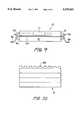
- FIG. 7illustrates an embodiment of the module or level-two package of the present invention with a top cap and bottom mounting adaptor
- FIG. 8illustrates an additional embodiment of the module or level-two package of the present invention with an intermediate lead frame
- FIG. 9illustrates an embodiment of the module or level-two package of the present invention with a bifurcated intermediate lead frame
- FIG. 10illustrates another embodiment of the module or level-two package of the present invention, with leads not shown, with heat conducting fins.
- the present inventionis for a bus communication system for a high density level-two package, or module, 10 shown in FIG. 1.
- Module 10is made up of a plurality of vertically stacked individual level-one integrated circuit packages 12.
- FIG. 1shows an embodiment with bifurcated distal lead ends 16.
- Each level-one package 12has leads 14 which extend from integrated circuit die 17 through a side wall 13 of the package casing 15.
- the leads 14have bifurcated distal lead ends 16, as shown in FIG. 2.
- Each distal lead end 16has a first finger 18 and a second finger 20. Either or both fingers of any lead end 16 may be removed during assembly of module 10, depending on the bus configuration desired.
- lead fingers 18 and 20 from adjacent stacked high density integrated circuit deuces 12 within module 10are electrically coupled.
- the distal lead ends 16 from adjacent level-one packages 12 which are physically and electrically connectedare formed so as to exert a mild spring load on each other to enhance physical and electrical contact.
- a module or level-two package 10may include a vertical stack of level-one packages 12 which contain trifurcated distal lead ends 22.
- Each trifurcated distal lead end 22has a first and second outside lead end finger 24 and a central lead end finger 26, shown in FIG. 4.
- the first or second outside lead end finger 24 of each stacked high density device 12is physically and electrically connected to an outside lead end finger 24 of an adjacent level-one package 12.
- the outside lead end fingers 24 of adjacent packages 12are pre-loaded to exert a mild spring load on each other to facilitate physical and electrical contact.
- intermediate stacked level-one packages 44an uppermost level-one package 46 and a lowermost level-one package 48.
- Distal lead ends 16 of each intermediate level-one package 44are physically and electrically connected to lead ends 16 of the level-one packages, one above and one below.
- the first or second lead end finger 18 or 20 of the lead ends 16 of each intermediate level-one package 44is physically and electrically connected to a corresponding first or second lead end finger 18 or 20 of the lead ends 16 of an adjacent uppermost 46, intermediate 44 or lowermost level-one package 48.
- the number of intermediate level-one packages 44 in any configurationmay vary, depending on the specific application involved.
- the lead ends 16 of the uppermost level-one package. 46 in FIG. 1 and the lowermost level-one package 48are physically and electrically connected only to the lead ends 16 of one adjacent intermediate level-one package 44. This connection is made by connecting either the first or second lead end finger 18 or 20 of the lead ends 16 of the uppermost package 46 and the lowermost package 48 to a corresponding first or second lead end finger 18 or 20 of the lead end 16 of the adjacent intermediate level-one package 44.
- the remaining first or second lead end finger 18 or 20 of the lead ends 16 of the lowermost level-one package 48can be removed or physically and electrically connected to an external signal pad 42 to provide an electronic communications link from module 10 to external electronic devices (not shown). Shown in FIG.
- the remaining first or second lead end finger 18 or 20 of the lead ends 16 of the uppermost level-one package 46can be physically and electrically connected to a heat spreader 36 disposed on the top surface of module 10.
- Heat spreader 36may also serve as a ground plane to reduce system noise.
- a rail-less bus systemis achieved for providing data communication between the individual high density level-one packages 12 within module 10, and between external electronic devices (not shown) and the level-one package 12 within module 10.
- Selective connections between leads of adjacent level-one packages and/or lead framescan be made by either removing the external lead ends not to be connected or by internally (inside the casing) disconnecting the non-selected leads during the manufacturing process.
- Selective interconnectioncan also be provided in a four-level stack, for example, by generating a set of four lead sets, one for each particular level. These level designated lead sets can be made from identical lead set stock which is modified by purchasing, etching or other suitable means.
- the bifurcation or trifurcation of the lead endscan begin at a point which is within the casing material.
- the level-one packages 12can be bound together to form a level-two module 10 by applying a thin, high temperature, thermally conductive adhesive material layer 28, shown in FIG. 6, between each vertically stacked high density device 12.
- the adhesive layer 28may be a high temperature silicon adhesive, such as du Pont KaptonTM two-sided adhesive tape, or a suitable high temperature epoxy adhesive.
- a high temperature adhesive band 30may be used.
- Band 30may be a continuous band of material which may be a high temperature silicon adhesive, du Pont KaptonTM tape, or an appropriate high temperature epoxy adhesive. Band 30 is preferably applied to module 10 so that it completely surrounds module 10.
- module 10may be applied to one or both ends of the module 10 using a high temperature epoxy adhesive or high temperature silicon adhesive to secure the level-one packages 12 together.
- the entire level-two package, or module, 10may be glued together using a high temperature silicon adhesive, or high temperature epoxy adhesive, to securely bond the level-one packages 12.
- module 10may be dipped in a conformal coating mixture. The conformal coating is then cured. All or some portion of the conformal coating may then be removed from the bottom of module 10 using known methods to allow module 10 to be securely fastened to an integrated circuit board header or other device or mounting platform.
- a bottom mounting adaptor 33(shown in FIG. 7) may be attached or mounted to module 10.
- Adaptor 33 for module 10may be a PCA adaptor which would allow module 10 to communicate with a greater variety of external electronic devices.
- the PGA adaptoralso would allow module 10 to be more easily socketed into a standard industry circuit board or device.
- band 30made of an appropriate high temperature silicon adhesive, double-sided KaptonTM tape or a suitable high temperature epoxy adhesive, may be used to assemble cap 32, adaptor 33, and all level-one packages 12 of module 10.
- a plurality of bands 30may also be used instead of a single band 30.
- Band 30applies pressure to cap 32 and adaptor 33 of module 10 while surrounding module 10, thereby securing the level-one packages 12 within module 10. The pressure exerted by band 30 also aids the bifurcated distal lead ends 16 in maintaining a mild spring force pressure against each other to thereby maintain better electrical contact.
- An intermediate lead frame 34in embodiments utilizing a lead-on-package (LOP) configuration, shown in FIGS. 8 and 9, may be disposed external to one or more level-one packages 12 in the level-two stack 10, causing frame 34 to be disposed between adjacent level-one packages 12 within module 10.
- Intermediate lead frame 34may contain bifurcated distal lead end 52 or trifurcated distal lead ends 22 (FIG. 4).
- the overall height of module 10is preferably less than 90 mils.
- the bifurcated lead ends 52 or trifurcated lead ends 22can be electrically connected to circuit conductive elements 50 extending through the sides of packages 12.
- a heat spreader 36may be disposed on the-top surface of module 10 to aid in heat dissipation from module 10.
- heat spreader 36is made of a high temperature thermally conductive material, such as metal, or a high temperature heat conductive plastic or composite material.
- Heat spreader 36may also include a plurality of fins 38 disposed on top of module 10, shown in FIG. 10.
- the fins 38may be made of heat conducting material, such as metal, high temperature plastic, or any other suitable high temperature conductive material.
- Mounting pads 40may be mounted to top cap of FIG. 7 of module 10 for surface mounting heat spreader 36 to module 10.
- Mounting pads 40may be mounted to top cap 32 by the use of any appropriate high temperature silicon adhesive, epoxy adhesive or KaptonTM tape. Alternatively, where top cap 32 is not used, mounting pads 40 may be surface mounted to the top surface of the uppermost level-one package in module 10. Heat spreader 36 can then be mounted to mounting pads 40 to aid heat dissipation from module 10.
- mounting pads 40may be first mounted to heat spreader 36 by the methods previously discussed. Heat spreader 36 may then be mounted to either top cap 32 of FIG. 7 or the top surface of the uppermost high density device 46 in module 10.
- Mounting pads 40may be made of a suitable high temperature thermally conductive material, such as KaptonTM tape, or other suitable material. Heat sink 36 should be attached to top cap 32 of FIG. 7 or the uppermost high density device 46 of module 10 before conformal coating or high temperature glue is applied to the upper surface of module 10. Mounting pads 40 may not easily adhere to the glue or conformal coating if the glue or conformal coating is applied to the upper surface of module 10 before mounting pads 40 are attached.
- circuit conductive elements 50which extend through side wall 13 of each integrated circuit level-one package, or device, 12 in module 10, are interleaved with and physically and electrically connected with bifurcated distal lead ends 52 of an intermediate lead frame 34.
- Intermediate lead frame 34is disposed externally to the protective casing surrounding package 12.
- a first lead end finger 58 of each bifurcated distal lead end. 52 of lead frame 34is electrically connected to a conductive element 50 of one level-one package 12 and the second lead end finger 56 of lead frame 34 is physically and electrically connected to the circuit conductive element 50 of an adjacent level-one package 12.
- the circuit conductive elements 50are Bent into physical and electrical contact with the respective lead end fingers 58 or 56 of bifurcated distal lead ends 52 of intermediate lead frame 34.
- Heat spreader 36if made of an electrically conductive material such as metal, may be electrically connected to module 10 power supply ground to reduce system noise for module 10. As shown in FIG. 5, a lead end finger 18 or 20 of each bifurcated distal lead end 16 of the level-one package 46 in module 10 may be physically and electrically connected heat spreader 36 to provide this ground connection.
- a lead end finger 18 or 20 of each lead 14 of the lowermost level-one package 48 in module 10may be electrically connected to an external signal pad 42 on the integrated circuit board (not shown) which contains module 10.
- the level-one packages 12 of module 10may communicate via the rail-less bus system to external electronic devices (not shown).
- an external bus communication systemis achieved as well as an internal bus communication system for data and other signal communication between the individual high density devices 12 of module 10.
Landscapes
- Engineering & Computer Science (AREA)
- Microelectronics & Electronic Packaging (AREA)
- Physics & Mathematics (AREA)
- Power Engineering (AREA)
- Condensed Matter Physics & Semiconductors (AREA)
- General Physics & Mathematics (AREA)
- Computer Hardware Design (AREA)
- Geometry (AREA)
- Lead Frames For Integrated Circuits (AREA)
Abstract
Description
Claims (1)
Priority Applications (2)
| Application Number | Priority Date | Filing Date | Title |
|---|---|---|---|
| US08/506,309US5552963A (en) | 1994-03-07 | 1995-07-24 | Bus communication system for stacked high density integrated circuit packages |
| US08/630,083US5586009A (en) | 1994-03-07 | 1996-04-09 | Bus communication system for stacked high density integrated circuit packages |
Applications Claiming Priority (3)
| Application Number | Priority Date | Filing Date | Title |
|---|---|---|---|
| US08/206,829US5455740A (en) | 1994-03-07 | 1994-03-07 | Bus communication system for stacked high density integrated circuit packages |
| US08/440,500US5479318A (en) | 1994-03-07 | 1995-05-12 | Bus communication system for stacked high density integrated circuit packages with trifurcated distal lead ends |
| US08/506,309US5552963A (en) | 1994-03-07 | 1995-07-24 | Bus communication system for stacked high density integrated circuit packages |
Related Parent Applications (1)
| Application Number | Title | Priority Date | Filing Date |
|---|---|---|---|
| US08/440,500DivisionUS5479318A (en) | 1994-03-07 | 1995-05-12 | Bus communication system for stacked high density integrated circuit packages with trifurcated distal lead ends |
Related Child Applications (1)
| Application Number | Title | Priority Date | Filing Date |
|---|---|---|---|
| US08/630,083ContinuationUS5586009A (en) | 1994-03-07 | 1996-04-09 | Bus communication system for stacked high density integrated circuit packages |
Publications (1)
| Publication Number | Publication Date |
|---|---|
| US5552963Atrue US5552963A (en) | 1996-09-03 |
Family
ID=22768152
Family Applications (6)
| Application Number | Title | Priority Date | Filing Date |
|---|---|---|---|
| US08/206,829Expired - LifetimeUS5455740A (en) | 1993-03-29 | 1994-03-07 | Bus communication system for stacked high density integrated circuit packages |
| US08/440,500Expired - LifetimeUS5479318A (en) | 1994-03-07 | 1995-05-12 | Bus communication system for stacked high density integrated circuit packages with trifurcated distal lead ends |
| US08/445,895Expired - Fee RelatedUS5605592A (en) | 1994-03-07 | 1995-05-22 | Method of manufacturing a bus communication system for stacked high density integrated circuit packages |
| US08/445,848Expired - LifetimeUS5493476A (en) | 1993-03-29 | 1995-05-22 | Bus communication system for stacked high density integrated circuit packages with bifurcated distal lead ends |
| US08/506,309Expired - Fee RelatedUS5552963A (en) | 1994-03-07 | 1995-07-24 | Bus communication system for stacked high density integrated circuit packages |
| US08/630,083Expired - Fee RelatedUS5586009A (en) | 1994-03-07 | 1996-04-09 | Bus communication system for stacked high density integrated circuit packages |
Family Applications Before (4)
| Application Number | Title | Priority Date | Filing Date |
|---|---|---|---|
| US08/206,829Expired - LifetimeUS5455740A (en) | 1993-03-29 | 1994-03-07 | Bus communication system for stacked high density integrated circuit packages |
| US08/440,500Expired - LifetimeUS5479318A (en) | 1994-03-07 | 1995-05-12 | Bus communication system for stacked high density integrated circuit packages with trifurcated distal lead ends |
| US08/445,895Expired - Fee RelatedUS5605592A (en) | 1994-03-07 | 1995-05-22 | Method of manufacturing a bus communication system for stacked high density integrated circuit packages |
| US08/445,848Expired - LifetimeUS5493476A (en) | 1993-03-29 | 1995-05-22 | Bus communication system for stacked high density integrated circuit packages with bifurcated distal lead ends |
Family Applications After (1)
| Application Number | Title | Priority Date | Filing Date |
|---|---|---|---|
| US08/630,083Expired - Fee RelatedUS5586009A (en) | 1994-03-07 | 1996-04-09 | Bus communication system for stacked high density integrated circuit packages |
Country Status (1)
| Country | Link |
|---|---|
| US (6) | US5455740A (en) |
Cited By (65)
| Publication number | Priority date | Publication date | Assignee | Title |
|---|---|---|---|---|
| US5691243A (en)* | 1995-05-15 | 1997-11-25 | Nec Corporation | Process for manufacturing composite semiconductor device |
| US5776797A (en)* | 1995-12-22 | 1998-07-07 | Fairchild Space And Defense Corporation | Three-dimensional flexible assembly of integrated circuits |
| US5837566A (en)* | 1994-06-23 | 1998-11-17 | Cubic Memory, Inc. | Vertical interconnect process for silicon segments |
| US5891761A (en)* | 1994-06-23 | 1999-04-06 | Cubic Memory, Inc. | Method for forming vertical interconnect process for silicon segments with thermally conductive epoxy preform |
| US5994170A (en)* | 1994-06-23 | 1999-11-30 | Cubic Memory, Inc. | Silicon segment programming method |
| US6080596A (en)* | 1994-06-23 | 2000-06-27 | Cubic Memory Inc. | Method for forming vertical interconnect process for silicon segments with dielectric isolation |
| US6121676A (en)* | 1996-12-13 | 2000-09-19 | Tessera, Inc. | Stacked microelectronic assembly and method therefor |
| US6124633A (en)* | 1994-06-23 | 2000-09-26 | Cubic Memory | Vertical interconnect process for silicon segments with thermally conductive epoxy preform |
| USRE36916E (en)* | 1995-03-21 | 2000-10-17 | Simple Technology Incorporated | Apparatus for stacking semiconductor chips |
| US6225691B1 (en)* | 1999-07-02 | 2001-05-01 | Cts Computer Technology System Corporation | Integrated circuit packaging structure |
| US6225689B1 (en) | 1998-08-21 | 2001-05-01 | Micron Technology, Inc. | Low profile multi-IC chip package connector |
| US6242285B1 (en) | 1998-07-23 | 2001-06-05 | Kyung Suk Kang | Stacked package of semiconductor package units via direct connection between leads and stacking method therefor |
| US6255726B1 (en) | 1994-06-23 | 2001-07-03 | Cubic Memory, Inc. | Vertical interconnect process for silicon segments with dielectric isolation |
| US20010006252A1 (en)* | 1996-12-13 | 2001-07-05 | Young Kim | Stacked microelectronic assembly and method therefor |
| US6281588B1 (en)* | 1995-09-12 | 2001-08-28 | Tessera, Inc. | Lead configurations |
| US6414396B1 (en) | 2000-01-24 | 2002-07-02 | Amkor Technology, Inc. | Package for stacked integrated circuits |
| US6462408B1 (en) | 2001-03-27 | 2002-10-08 | Staktek Group, L.P. | Contact member stacking system and method |
| US6483736B2 (en) | 1998-11-16 | 2002-11-19 | Matrix Semiconductor, Inc. | Vertically stacked field programmable nonvolatile memory and method of fabrication |
| US6486528B1 (en) | 1994-06-23 | 2002-11-26 | Vertical Circuits, Inc. | Silicon segment programming apparatus and three terminal fuse configuration |
| US20030030074A1 (en)* | 2001-08-13 | 2003-02-13 | Walker Andrew J | TFT mask ROM and method for making same |
| US6521483B1 (en)* | 1999-07-22 | 2003-02-18 | Seiko Epson Corporation | Semiconductor device, method of manufacture thereof, circuit board, and electronic device |
| US6525953B1 (en) | 2001-08-13 | 2003-02-25 | Matrix Semiconductor, Inc. | Vertically-stacked, field-programmable, nonvolatile memory and method of fabrication |
| US20030107118A1 (en)* | 2001-10-09 | 2003-06-12 | Tessera, Inc. | Stacked packages |
| US6593624B2 (en) | 2001-09-25 | 2003-07-15 | Matrix Semiconductor, Inc. | Thin film transistors with vertically offset drain regions |
| US6608763B1 (en) | 2000-09-15 | 2003-08-19 | Staktek Group L.P. | Stacking system and method |
| US20030168725A1 (en)* | 1996-12-13 | 2003-09-11 | Tessera, Inc. | Methods of making microelectronic assemblies including folded substrates |
| US6624485B2 (en) | 2001-11-05 | 2003-09-23 | Matrix Semiconductor, Inc. | Three-dimensional, mask-programmed read only memory |
| US6731011B2 (en) | 2002-02-19 | 2004-05-04 | Matrix Semiconductor, Inc. | Memory module having interconnected and stacked integrated circuits |
| US6737675B2 (en) | 2002-06-27 | 2004-05-18 | Matrix Semiconductor, Inc. | High density 3D rail stack arrays |
| US20040099938A1 (en)* | 2002-09-11 | 2004-05-27 | Tessera, Inc. | Assemblies having stacked semiconductor chips and methods of making same |
| US20040104470A1 (en)* | 2002-08-16 | 2004-06-03 | Tessera, Inc. | Microelectronic packages with self-aligning features |
| US20040108583A1 (en)* | 2002-12-05 | 2004-06-10 | Roeters Glen E. | Thin scale outline package stack |
| US20040217461A1 (en)* | 2002-08-05 | 2004-11-04 | Tessera, Inc. | Microelectronic adaptors, assemblies and methods |
| US6843421B2 (en) | 2001-08-13 | 2005-01-18 | Matrix Semiconductor, Inc. | Molded memory module and method of making the module absent a substrate support |
| US6853049B2 (en) | 2002-03-13 | 2005-02-08 | Matrix Semiconductor, Inc. | Silicide-silicon oxide-semiconductor antifuse device and method of making |
| US6881994B2 (en) | 2000-08-14 | 2005-04-19 | Matrix Semiconductor, Inc. | Monolithic three dimensional array of charge storage devices containing a planarized surface |
| US6885106B1 (en) | 2001-01-11 | 2005-04-26 | Tessera, Inc. | Stacked microelectronic assemblies and methods of making same |
| US6888750B2 (en) | 2000-04-28 | 2005-05-03 | Matrix Semiconductor, Inc. | Nonvolatile memory on SOI and compound semiconductor substrates and method of fabrication |
| US6897514B2 (en) | 2001-03-28 | 2005-05-24 | Matrix Semiconductor, Inc. | Two mask floating gate EEPROM and method of making |
| US6919626B2 (en) | 1992-12-11 | 2005-07-19 | Staktek Group L.P. | High density integrated circuit module |
| US20050224952A1 (en)* | 2004-04-13 | 2005-10-13 | Al Vindasius | Three dimensional six surface conformal die coating |
| US20050258530A1 (en)* | 2004-04-13 | 2005-11-24 | Al Vindasius | Micropede stacked die component assembly |
| US6977440B2 (en) | 2001-10-09 | 2005-12-20 | Tessera, Inc. | Stacked packages |
| US7066741B2 (en) | 1999-09-24 | 2006-06-27 | Staktek Group L.P. | Flexible circuit connector for stacked chip module |
| US7215018B2 (en) | 2004-04-13 | 2007-05-08 | Vertical Circuits, Inc. | Stacked die BGA or LGA component assembly |
| US20080042274A1 (en)* | 2002-09-06 | 2008-02-21 | Tessera, Inc. | Components, methods and assemblies for stacked packages |
| US7335995B2 (en) | 2001-10-09 | 2008-02-26 | Tessera, Inc. | Microelectronic assembly having array including passive elements and interconnects |
| US7352199B2 (en) | 2001-02-20 | 2008-04-01 | Sandisk Corporation | Memory card with enhanced testability and methods of making and using the same |
| US20080122113A1 (en)* | 2006-08-17 | 2008-05-29 | Corisis David J | Semiconductor device assemblies and systems including at least one conductive pathway extending around a side of at least one semiconductor device and methods for forming the same |
| US7545029B2 (en) | 2006-08-18 | 2009-06-09 | Tessera, Inc. | Stack microelectronic assemblies |
| US20100193970A1 (en)* | 2003-12-30 | 2010-08-05 | Tessera, Inc. | Micro pin grid array with pin motion isolation |
| US8575719B2 (en) | 2000-04-28 | 2013-11-05 | Sandisk 3D Llc | Silicon nitride antifuse for use in diode-antifuse memory arrays |
| US8580607B2 (en) | 2010-07-27 | 2013-11-12 | Tessera, Inc. | Microelectronic packages with nanoparticle joining |
| US8604348B2 (en) | 2003-10-06 | 2013-12-10 | Tessera, Inc. | Method of making a connection component with posts and pads |
| US8641913B2 (en) | 2003-10-06 | 2014-02-04 | Tessera, Inc. | Fine pitch microcontacts and method for forming thereof |
| US8723318B2 (en) | 2010-07-08 | 2014-05-13 | Tessera, Inc. | Microelectronic packages with dual or multiple-etched flip-chip connectors |
| US8853558B2 (en) | 2010-12-10 | 2014-10-07 | Tessera, Inc. | Interconnect structure |
| US8884448B2 (en) | 2007-09-28 | 2014-11-11 | Tessera, Inc. | Flip chip interconnection with double post |
| USRE45463E1 (en) | 2003-11-12 | 2015-04-14 | Tessera, Inc. | Stacked microelectronic assemblies with central contacts |
| US9478495B1 (en) | 2015-10-26 | 2016-10-25 | Sandisk Technologies Llc | Three dimensional memory device containing aluminum source contact via structure and method of making thereof |
| US9627395B2 (en) | 2015-02-11 | 2017-04-18 | Sandisk Technologies Llc | Enhanced channel mobility three-dimensional memory structure and method of making thereof |
| US9633971B2 (en) | 2015-07-10 | 2017-04-25 | Invensas Corporation | Structures and methods for low temperature bonding using nanoparticles |
| US10535626B2 (en) | 2015-07-10 | 2020-01-14 | Invensas Corporation | Structures and methods for low temperature bonding using nanoparticles |
| US11973056B2 (en) | 2016-10-27 | 2024-04-30 | Adeia Semiconductor Technologies Llc | Methods for low temperature bonding using nanoparticles |
| US12211809B2 (en) | 2020-12-30 | 2025-01-28 | Adeia Semiconductor Bonding Technologies Inc. | Structure with conductive feature and method of forming same |
Families Citing this family (70)
| Publication number | Priority date | Publication date | Assignee | Title |
|---|---|---|---|---|
| US5484959A (en)* | 1992-12-11 | 1996-01-16 | Staktek Corporation | High density lead-on-package fabrication method and apparatus |
| US5369056A (en)* | 1993-03-29 | 1994-11-29 | Staktek Corporation | Warp-resistent ultra-thin integrated circuit package fabrication method |
| KR0144283B1 (en)* | 1993-10-28 | 1998-07-15 | 쯔지 하루오 | Structure and method for mounting panel and flexible wiring board, and driver ic exchange method |
| US5870290A (en)* | 1994-11-30 | 1999-02-09 | Intel Corporation | Interface adapter board having arrays of interstitial connectors and an intermediate switching circuit |
| US5861666A (en)* | 1995-08-30 | 1999-01-19 | Tessera, Inc. | Stacked chip assembly |
| DE19639025C2 (en) | 1996-09-23 | 1999-10-28 | Siemens Ag | Chip module and method for producing a chip module |
| US5925927A (en)* | 1996-12-18 | 1999-07-20 | Texas Instruments Incoporated | Reinforced thin lead frames and leads |
| US5903437A (en)* | 1997-01-17 | 1999-05-11 | International Business Machines Corporation | High density edge mounting of chips |
| US5818107A (en)* | 1997-01-17 | 1998-10-06 | International Business Machines Corporation | Chip stacking by edge metallization |
| US6058443A (en)* | 1997-02-18 | 2000-05-02 | Advanced Micro Devices, Inc. | System for partitioning PC chipset functions into logic and port integrated circuits |
| US5974492A (en)* | 1997-02-18 | 1999-10-26 | Advanced Micro Devices, Inc. | Method for input/output port replication using an interconnection bus |
| US5926629A (en)* | 1997-02-18 | 1999-07-20 | Advanced Micro Devices, Inc. | Continuously operating interconnection bus |
| US6028352A (en)* | 1997-06-13 | 2000-02-22 | Irvine Sensors Corporation | IC stack utilizing secondary leadframes |
| JPH1197619A (en)* | 1997-07-25 | 1999-04-09 | Oki Electric Ind Co Ltd | Semiconductor device, manufacture thereof and mounting thereof |
| JP3063720B2 (en)* | 1997-12-12 | 2000-07-12 | 日本電気株式会社 | Busbar structure with noise filter function |
| DE19833713C1 (en)* | 1998-07-27 | 2000-05-04 | Siemens Ag | Laminate or stacked package arrangement based on at least two integrated circuits |
| US6049467A (en)* | 1998-08-31 | 2000-04-11 | Unisys Corporation | Stackable high density RAM modules |
| US6093029A (en)* | 1998-09-08 | 2000-07-25 | S3 Incorporated | Vertically stackable integrated circuit |
| US6295220B1 (en) | 1998-11-03 | 2001-09-25 | Zomaya Group, Inc. | Memory bar and related circuits and methods |
| US6190425B1 (en) | 1998-11-03 | 2001-02-20 | Zomaya Group, Inc. | Memory bar and related circuits and methods |
| IL143962A0 (en)* | 1999-01-08 | 2002-04-21 | Emisphere Tech Inc | Polymeric delivery agents and delivery agent compounds |
| DE19933265A1 (en)* | 1999-07-15 | 2001-02-01 | Siemens Ag | TSOP memory chip package assembly |
| US6713854B1 (en) | 2000-10-16 | 2004-03-30 | Legacy Electronics, Inc | Electronic circuit module with a carrier having a mounting pad array |
| US7102892B2 (en) | 2000-03-13 | 2006-09-05 | Legacy Electronics, Inc. | Modular integrated circuit chip carrier |
| US6545868B1 (en)* | 2000-03-13 | 2003-04-08 | Legacy Electronics, Inc. | Electronic module having canopy-type carriers |
| US7337522B2 (en) | 2000-10-16 | 2008-03-04 | Legacy Electronics, Inc. | Method and apparatus for fabricating a circuit board with a three dimensional surface mounted array of semiconductor chips |
| WO2002074024A2 (en) | 2001-03-14 | 2002-09-19 | Legacy Electronics, Inc. | A method and apparatus for fabricating a circuit board with a three dimensional surface mounted array of semiconductor chips |
| US6627980B2 (en)* | 2001-04-12 | 2003-09-30 | Formfactor, Inc. | Stacked semiconductor device assembly with microelectronic spring contacts |
| US6956284B2 (en)* | 2001-10-26 | 2005-10-18 | Staktek Group L.P. | Integrated circuit stacking system and method |
| US7202555B2 (en) | 2001-10-26 | 2007-04-10 | Staktek Group L.P. | Pitch change and chip scale stacking system and method |
| US7026708B2 (en) | 2001-10-26 | 2006-04-11 | Staktek Group L.P. | Low profile chip scale stacking system and method |
| US20030234443A1 (en) | 2001-10-26 | 2003-12-25 | Staktek Group, L.P. | Low profile stacking system and method |
| US7656678B2 (en) | 2001-10-26 | 2010-02-02 | Entorian Technologies, Lp | Stacked module systems |
| US6914324B2 (en)* | 2001-10-26 | 2005-07-05 | Staktek Group L.P. | Memory expansion and chip scale stacking system and method |
| US7371609B2 (en) | 2001-10-26 | 2008-05-13 | Staktek Group L.P. | Stacked module systems and methods |
| US20050056921A1 (en)* | 2003-09-15 | 2005-03-17 | Staktek Group L.P. | Stacked module systems and methods |
| US20040195666A1 (en)* | 2001-10-26 | 2004-10-07 | Julian Partridge | Stacked module systems and methods |
| US6940729B2 (en) | 2001-10-26 | 2005-09-06 | Staktek Group L.P. | Integrated circuit stacking system and method |
| US7053478B2 (en) | 2001-10-26 | 2006-05-30 | Staktek Group L.P. | Pitch change and chip scale stacking system |
| US7485951B2 (en)* | 2001-10-26 | 2009-02-03 | Entorian Technologies, Lp | Modularized die stacking system and method |
| US6576992B1 (en) | 2001-10-26 | 2003-06-10 | Staktek Group L.P. | Chip scale stacking system and method |
| US20050009234A1 (en)* | 2001-10-26 | 2005-01-13 | Staktek Group, L.P. | Stacked module systems and methods for CSP packages |
| US7081373B2 (en) | 2001-12-14 | 2006-07-25 | Staktek Group, L.P. | CSP chip stack with flex circuit |
| KR100462991B1 (en)* | 2002-03-11 | 2004-12-23 | 최영인 | Manufacturing method and device of stacking IC package |
| US6952047B2 (en)* | 2002-07-01 | 2005-10-04 | Tessera, Inc. | Assemblies having stacked semiconductor chips and methods of making same |
| US20050167817A1 (en)* | 2002-08-05 | 2005-08-04 | Tessera, Inc. | Microelectronic adaptors, assemblies and methods |
| US6841029B2 (en)* | 2003-03-27 | 2005-01-11 | Advanced Cardiovascular Systems, Inc. | Surface modification of expanded ultra high molecular weight polyethylene (eUHMWPE) for improved bondability |
| US20040245615A1 (en)* | 2003-06-03 | 2004-12-09 | Staktek Group, L.P. | Point to point memory expansion system and method |
| US20060033187A1 (en)* | 2004-08-12 | 2006-02-16 | Staktek Group, L.P. | Rugged CSP module system and method |
| US20060043558A1 (en)* | 2004-09-01 | 2006-03-02 | Staktek Group L.P. | Stacked integrated circuit cascade signaling system and method |
| US20060055024A1 (en)* | 2004-09-14 | 2006-03-16 | Staktek Group, L.P. | Adapted leaded integrated circuit module |
| US20060072297A1 (en)* | 2004-10-01 | 2006-04-06 | Staktek Group L.P. | Circuit Module Access System and Method |
| US20060118936A1 (en)* | 2004-12-03 | 2006-06-08 | Staktek Group L.P. | Circuit module component mounting system and method |
| WO2006076381A2 (en) | 2005-01-12 | 2006-07-20 | Legacy Electronics, Inc. | Radial circuit board, system, and methods |
| US7309914B2 (en) | 2005-01-20 | 2007-12-18 | Staktek Group L.P. | Inverted CSP stacking system and method |
| US20060175693A1 (en)* | 2005-02-04 | 2006-08-10 | Staktek Group, L.P. | Systems, methods, and apparatus for generating ball-out matrix configuration output for a flex circuit |
| US20060244114A1 (en)* | 2005-04-28 | 2006-11-02 | Staktek Group L.P. | Systems, methods, and apparatus for connecting a set of contacts on an integrated circuit to a flex circuit via a contact beam |
| US7033861B1 (en) | 2005-05-18 | 2006-04-25 | Staktek Group L.P. | Stacked module systems and method |
| US7576995B2 (en) | 2005-11-04 | 2009-08-18 | Entorian Technologies, Lp | Flex circuit apparatus and method for adding capacitance while conserving circuit board surface area |
| US7605454B2 (en) | 2006-01-11 | 2009-10-20 | Entorian Technologies, Lp | Memory card and method for devising |
| US7508058B2 (en) | 2006-01-11 | 2009-03-24 | Entorian Technologies, Lp | Stacked integrated circuit module |
| US7608920B2 (en) | 2006-01-11 | 2009-10-27 | Entorian Technologies, Lp | Memory card and method for devising |
| US7508069B2 (en) | 2006-01-11 | 2009-03-24 | Entorian Technologies, Lp | Managed memory component |
| US7304382B2 (en) | 2006-01-11 | 2007-12-04 | Staktek Group L.P. | Managed memory component |
| US7727816B2 (en)* | 2006-07-21 | 2010-06-01 | Stats Chippac Ltd. | Integrated circuit package system with offset stacked die |
| US7468553B2 (en) | 2006-10-20 | 2008-12-23 | Entorian Technologies, Lp | Stackable micropackages and stacked modules |
| US7763983B2 (en)* | 2007-07-02 | 2010-07-27 | Tessera, Inc. | Stackable microelectronic device carriers, stacked device carriers and methods of making the same |
| JP6082985B2 (en)* | 2013-02-07 | 2017-02-22 | パナソニックIpマネジメント株式会社 | Semiconductor device, electronic circuit device, compressor |
| DE102015008503A1 (en)* | 2015-07-03 | 2017-01-05 | TE Connectivity Sensors Germany GmbH | Electrical component and manufacturing method for producing such an electrical component |
| US9917041B1 (en)* | 2016-10-28 | 2018-03-13 | Intel Corporation | 3D chip assemblies using stacked leadframes |
Citations (19)
| Publication number | Priority date | Publication date | Assignee | Title |
|---|---|---|---|---|
| US3746934A (en)* | 1971-05-06 | 1973-07-17 | Siemens Ag | Stack arrangement of semiconductor chips |
| JPS5896756A (en)* | 1981-12-04 | 1983-06-08 | Toshiba Corp | multi-chip package |
| JPS58112348A (en)* | 1981-12-25 | 1983-07-04 | Fujitsu Ltd | semiconductor equipment |
| US4398235A (en)* | 1980-09-11 | 1983-08-09 | General Motors Corporation | Vertical integrated circuit package integration |
| US4521828A (en)* | 1982-12-23 | 1985-06-04 | At&T Technologies, Inc. | Component module for piggyback mounting on a circuit package having dual-in-line leads |
| US4763188A (en)* | 1986-08-08 | 1988-08-09 | Thomas Johnson | Packaging system for multiple semiconductor devices |
| US4796078A (en)* | 1987-06-15 | 1989-01-03 | International Business Machines Corporation | Peripheral/area wire bonding technique |
| EP0298211A2 (en)* | 1987-07-06 | 1989-01-11 | International Business Machines Corporation | Ceramic card assembly having enhanced power distribution and cooling |
| US4884237A (en)* | 1984-03-28 | 1989-11-28 | International Business Machines Corporation | Stacked double density memory module using industry standard memory chips |
| US4953060A (en)* | 1989-05-05 | 1990-08-28 | Ncr Corporation | Stackable integrated circuit chip package with improved heat removal |
| US4956694A (en)* | 1988-11-04 | 1990-09-11 | Dense-Pac Microsystems, Inc. | Integrated circuit chip stacking |
| JPH0471260A (en)* | 1990-07-12 | 1992-03-05 | Ibiden Co Ltd | Electronic part |
| US5151559A (en)* | 1991-05-02 | 1992-09-29 | International Business Machines Corporation | Planarized thin film surface covered wire bonded semiconductor package |
| US5221642A (en)* | 1991-08-15 | 1993-06-22 | Staktek Corporation | Lead-on-chip integrated circuit fabrication method |
| US5270492A (en)* | 1991-08-26 | 1993-12-14 | Rohm Co., Ltd. | Structure of lead terminal of electronic device |
| JPH05343610A (en)* | 1992-06-11 | 1993-12-24 | Hitachi Ltd | Hybrid integrated circuit device |
| US5279029A (en)* | 1990-08-01 | 1994-01-18 | Staktek Corporation | Ultra high density integrated circuit packages method |
| US5367766A (en)* | 1990-08-01 | 1994-11-29 | Staktek Corporation | Ultra high density integrated circuit packages method |
| US5394010A (en)* | 1991-03-13 | 1995-02-28 | Kabushiki Kaisha Toshiba | Semiconductor assembly having laminated semiconductor devices |
Family Cites Families (1)
| Publication number | Priority date | Publication date | Assignee | Title |
|---|---|---|---|---|
| US4961806A (en)* | 1986-12-10 | 1990-10-09 | Sanders Associates, Inc. | Method of making a printed circuit |
- 1994
- 1994-03-07USUS08/206,829patent/US5455740A/ennot_activeExpired - Lifetime
- 1995
- 1995-05-12USUS08/440,500patent/US5479318A/ennot_activeExpired - Lifetime
- 1995-05-22USUS08/445,895patent/US5605592A/ennot_activeExpired - Fee Related
- 1995-05-22USUS08/445,848patent/US5493476A/ennot_activeExpired - Lifetime
- 1995-07-24USUS08/506,309patent/US5552963A/ennot_activeExpired - Fee Related
- 1996
- 1996-04-09USUS08/630,083patent/US5586009A/ennot_activeExpired - Fee Related
Patent Citations (19)
| Publication number | Priority date | Publication date | Assignee | Title |
|---|---|---|---|---|
| US3746934A (en)* | 1971-05-06 | 1973-07-17 | Siemens Ag | Stack arrangement of semiconductor chips |
| US4398235A (en)* | 1980-09-11 | 1983-08-09 | General Motors Corporation | Vertical integrated circuit package integration |
| JPS5896756A (en)* | 1981-12-04 | 1983-06-08 | Toshiba Corp | multi-chip package |
| JPS58112348A (en)* | 1981-12-25 | 1983-07-04 | Fujitsu Ltd | semiconductor equipment |
| US4521828A (en)* | 1982-12-23 | 1985-06-04 | At&T Technologies, Inc. | Component module for piggyback mounting on a circuit package having dual-in-line leads |
| US4884237A (en)* | 1984-03-28 | 1989-11-28 | International Business Machines Corporation | Stacked double density memory module using industry standard memory chips |
| US4763188A (en)* | 1986-08-08 | 1988-08-09 | Thomas Johnson | Packaging system for multiple semiconductor devices |
| US4796078A (en)* | 1987-06-15 | 1989-01-03 | International Business Machines Corporation | Peripheral/area wire bonding technique |
| EP0298211A2 (en)* | 1987-07-06 | 1989-01-11 | International Business Machines Corporation | Ceramic card assembly having enhanced power distribution and cooling |
| US4956694A (en)* | 1988-11-04 | 1990-09-11 | Dense-Pac Microsystems, Inc. | Integrated circuit chip stacking |
| US4953060A (en)* | 1989-05-05 | 1990-08-28 | Ncr Corporation | Stackable integrated circuit chip package with improved heat removal |
| JPH0471260A (en)* | 1990-07-12 | 1992-03-05 | Ibiden Co Ltd | Electronic part |
| US5279029A (en)* | 1990-08-01 | 1994-01-18 | Staktek Corporation | Ultra high density integrated circuit packages method |
| US5367766A (en)* | 1990-08-01 | 1994-11-29 | Staktek Corporation | Ultra high density integrated circuit packages method |
| US5394010A (en)* | 1991-03-13 | 1995-02-28 | Kabushiki Kaisha Toshiba | Semiconductor assembly having laminated semiconductor devices |
| US5151559A (en)* | 1991-05-02 | 1992-09-29 | International Business Machines Corporation | Planarized thin film surface covered wire bonded semiconductor package |
| US5221642A (en)* | 1991-08-15 | 1993-06-22 | Staktek Corporation | Lead-on-chip integrated circuit fabrication method |
| US5270492A (en)* | 1991-08-26 | 1993-12-14 | Rohm Co., Ltd. | Structure of lead terminal of electronic device |
| JPH05343610A (en)* | 1992-06-11 | 1993-12-24 | Hitachi Ltd | Hybrid integrated circuit device |
Non-Patent Citations (1)
| Title |
|---|
| Information allegedly written by Emory Garth regarding Memory Stacks, Applicant received a facsimile from Emory Garth on Jan. 26, 1993, Applicant does not know when the information was written or its validity.* |
Cited By (141)
| Publication number | Priority date | Publication date | Assignee | Title |
|---|---|---|---|---|
| US6919626B2 (en) | 1992-12-11 | 2005-07-19 | Staktek Group L.P. | High density integrated circuit module |
| US6188126B1 (en) | 1994-06-23 | 2001-02-13 | Cubic Memory Inc. | Vertical interconnect process for silicon segments |
| US6486528B1 (en) | 1994-06-23 | 2002-11-26 | Vertical Circuits, Inc. | Silicon segment programming apparatus and three terminal fuse configuration |
| US5891761A (en)* | 1994-06-23 | 1999-04-06 | Cubic Memory, Inc. | Method for forming vertical interconnect process for silicon segments with thermally conductive epoxy preform |
| US5994170A (en)* | 1994-06-23 | 1999-11-30 | Cubic Memory, Inc. | Silicon segment programming method |
| US6080596A (en)* | 1994-06-23 | 2000-06-27 | Cubic Memory Inc. | Method for forming vertical interconnect process for silicon segments with dielectric isolation |
| US6255726B1 (en) | 1994-06-23 | 2001-07-03 | Cubic Memory, Inc. | Vertical interconnect process for silicon segments with dielectric isolation |
| US6124633A (en)* | 1994-06-23 | 2000-09-26 | Cubic Memory | Vertical interconnect process for silicon segments with thermally conductive epoxy preform |
| US5837566A (en)* | 1994-06-23 | 1998-11-17 | Cubic Memory, Inc. | Vertical interconnect process for silicon segments |
| USRE36916E (en)* | 1995-03-21 | 2000-10-17 | Simple Technology Incorporated | Apparatus for stacking semiconductor chips |
| US5691243A (en)* | 1995-05-15 | 1997-11-25 | Nec Corporation | Process for manufacturing composite semiconductor device |
| US6281588B1 (en)* | 1995-09-12 | 2001-08-28 | Tessera, Inc. | Lead configurations |
| US6420661B1 (en) | 1995-09-12 | 2002-07-16 | Tessera, Inc. | Connector element for connecting microelectronic elements |
| US6570101B2 (en) | 1995-09-12 | 2003-05-27 | Tessera, Inc. | Lead configurations |
| US5776797A (en)* | 1995-12-22 | 1998-07-07 | Fairchild Space And Defense Corporation | Three-dimensional flexible assembly of integrated circuits |
| US20010006252A1 (en)* | 1996-12-13 | 2001-07-05 | Young Kim | Stacked microelectronic assembly and method therefor |
| US7149095B2 (en) | 1996-12-13 | 2006-12-12 | Tessera, Inc. | Stacked microelectronic assemblies |
| US6121676A (en)* | 1996-12-13 | 2000-09-19 | Tessera, Inc. | Stacked microelectronic assembly and method therefor |
| US20030168725A1 (en)* | 1996-12-13 | 2003-09-11 | Tessera, Inc. | Methods of making microelectronic assemblies including folded substrates |
| US6699730B2 (en) | 1996-12-13 | 2004-03-02 | Tessers, Inc. | Stacked microelectronic assembly and method therefor |
| US6242285B1 (en) | 1998-07-23 | 2001-06-05 | Kyung Suk Kang | Stacked package of semiconductor package units via direct connection between leads and stacking method therefor |
| US6475831B2 (en) | 1998-08-21 | 2002-11-05 | Micron Technology, Inc. | Methods for a low profile multi-IC chip package connector |
| US20060252180A1 (en)* | 1998-08-21 | 2006-11-09 | Moden Walter L | Method for a low profile multi-IC chip package connector |
| US6225689B1 (en) | 1998-08-21 | 2001-05-01 | Micron Technology, Inc. | Low profile multi-IC chip package connector |
| US6486546B2 (en) | 1998-08-21 | 2002-11-26 | Micron Technology, Inc. | Low profile multi-IC chip package connector |
| US20040168316A1 (en)* | 1998-08-21 | 2004-09-02 | Moden Walter L. | Low profile multi-IC chip package connector |
| US6773955B2 (en) | 1998-08-21 | 2004-08-10 | Micron Technology, Inc. | Low profile multi-IC chip package connector |
| US20080003712A1 (en)* | 1998-08-21 | 2008-01-03 | Moden Walter L | Methods of making semiconductor fuses |
| US6258623B1 (en)* | 1998-08-21 | 2001-07-10 | Micron Technology, Inc. | Low profile multi-IC chip package connector |
| US6362519B2 (en) | 1998-08-21 | 2002-03-26 | Micron Technology, Inc. | Low profile multi-IC chip package connector |
| US6686655B2 (en) | 1998-08-21 | 2004-02-03 | Micron Technology, Inc. | Low profile multi-IC chip package connector |
| US8897056B2 (en) | 1998-11-16 | 2014-11-25 | Sandisk 3D Llc | Pillar-shaped nonvolatile memory and method of fabrication |
| US6483736B2 (en) | 1998-11-16 | 2002-11-19 | Matrix Semiconductor, Inc. | Vertically stacked field programmable nonvolatile memory and method of fabrication |
| US8208282B2 (en) | 1998-11-16 | 2012-06-26 | Sandisk 3D Llc | Vertically stacked field programmable nonvolatile memory and method of fabrication |
| US7816189B2 (en) | 1998-11-16 | 2010-10-19 | Sandisk 3D Llc | Vertically stacked field programmable nonvolatile memory and method of fabrication |
| US8503215B2 (en) | 1998-11-16 | 2013-08-06 | Sandisk 3D Llc | Vertically stacked field programmable nonvolatile memory and method of fabrication |
| US7319053B2 (en) | 1998-11-16 | 2008-01-15 | Sandisk 3D Llc | Vertically stacked field programmable nonvolatile memory and method of fabrication |
| US20060134837A1 (en)* | 1998-11-16 | 2006-06-22 | Vivek Subramanian | Vertically stacked field programmable nonvolatile memory and method of fabrication |
| US9214243B2 (en) | 1998-11-16 | 2015-12-15 | Sandisk 3D Llc | Three-dimensional nonvolatile memory and method of fabrication |
| US7283403B2 (en) | 1998-11-16 | 2007-10-16 | Sandisk 3D Llc | Memory device and method for simultaneously programming and/or reading memory cells on different levels |
| US7265000B2 (en) | 1998-11-16 | 2007-09-04 | Sandisk 3D Llc | Vertically stacked field programmable nonvolatile memory and method of fabrication |
| US7190602B2 (en) | 1998-11-16 | 2007-03-13 | Sandisk 3D Llc | Integrated circuit incorporating three-dimensional memory array with dual opposing decoder arrangement |
| US7160761B2 (en) | 1998-11-16 | 2007-01-09 | Sandisk 3D Llc | Vertically stacked field programmable nonvolatile memory and method of fabrication |
| US7978492B2 (en) | 1998-11-16 | 2011-07-12 | Sandisk 3D Llc | Integrated circuit incorporating decoders disposed beneath memory arrays |
| US6780711B2 (en) | 1998-11-16 | 2004-08-24 | Matrix Semiconductor, Inc | Vertically stacked field programmable nonvolatile memory and method of fabrication |
| US20030016553A1 (en)* | 1998-11-16 | 2003-01-23 | Vivek Subramanian | Vertically stacked field programmable nonvolatile memory and method of fabrication |
| US7157314B2 (en) | 1998-11-16 | 2007-01-02 | Sandisk Corporation | Vertically stacked field programmable nonvolatile memory and method of fabrication |
| US6225691B1 (en)* | 1999-07-02 | 2001-05-01 | Cts Computer Technology System Corporation | Integrated circuit packaging structure |
| US6521483B1 (en)* | 1999-07-22 | 2003-02-18 | Seiko Epson Corporation | Semiconductor device, method of manufacture thereof, circuit board, and electronic device |
| US7066741B2 (en) | 1999-09-24 | 2006-06-27 | Staktek Group L.P. | Flexible circuit connector for stacked chip module |
| US6414396B1 (en) | 2000-01-24 | 2002-07-02 | Amkor Technology, Inc. | Package for stacked integrated circuits |
| US6888750B2 (en) | 2000-04-28 | 2005-05-03 | Matrix Semiconductor, Inc. | Nonvolatile memory on SOI and compound semiconductor substrates and method of fabrication |
| US8575719B2 (en) | 2000-04-28 | 2013-11-05 | Sandisk 3D Llc | Silicon nitride antifuse for use in diode-antifuse memory arrays |
| US7129538B2 (en) | 2000-08-14 | 2006-10-31 | Sandisk 3D Llc | Dense arrays and charge storage devices |
| US9171857B2 (en) | 2000-08-14 | 2015-10-27 | Sandisk 3D Llc | Dense arrays and charge storage devices |
| US6881994B2 (en) | 2000-08-14 | 2005-04-19 | Matrix Semiconductor, Inc. | Monolithic three dimensional array of charge storage devices containing a planarized surface |
| US8981457B2 (en) | 2000-08-14 | 2015-03-17 | Sandisk 3D Llc | Dense arrays and charge storage devices |
| US7825455B2 (en) | 2000-08-14 | 2010-11-02 | Sandisk 3D Llc | Three terminal nonvolatile memory device with vertical gated diode |
| US9559110B2 (en) | 2000-08-14 | 2017-01-31 | Sandisk Technologies Llc | Dense arrays and charge storage devices |
| US6992349B2 (en) | 2000-08-14 | 2006-01-31 | Matrix Semiconductor, Inc. | Rail stack array of charge storage devices and method of making same |
| US8823076B2 (en) | 2000-08-14 | 2014-09-02 | Sandisk 3D Llc | Dense arrays and charge storage devices |
| US10644021B2 (en) | 2000-08-14 | 2020-05-05 | Sandisk Technologies Llc | Dense arrays and charge storage devices |
| US10008511B2 (en) | 2000-08-14 | 2018-06-26 | Sandisk Technologies Llc | Dense arrays and charge storage devices |
| US8853765B2 (en) | 2000-08-14 | 2014-10-07 | Sandisk 3D Llc | Dense arrays and charge storage devices |
| US6608763B1 (en) | 2000-09-15 | 2003-08-19 | Staktek Group L.P. | Stacking system and method |
| US6885106B1 (en) | 2001-01-11 | 2005-04-26 | Tessera, Inc. | Stacked microelectronic assemblies and methods of making same |
| US7352199B2 (en) | 2001-02-20 | 2008-04-01 | Sandisk Corporation | Memory card with enhanced testability and methods of making and using the same |
| US6806120B2 (en) | 2001-03-27 | 2004-10-19 | Staktek Group, L.P. | Contact member stacking system and method |
| US6462408B1 (en) | 2001-03-27 | 2002-10-08 | Staktek Group, L.P. | Contact member stacking system and method |
| US7615436B2 (en) | 2001-03-28 | 2009-11-10 | Sandisk 3D Llc | Two mask floating gate EEPROM and method of making |
| US6897514B2 (en) | 2001-03-28 | 2005-05-24 | Matrix Semiconductor, Inc. | Two mask floating gate EEPROM and method of making |
| US6843421B2 (en) | 2001-08-13 | 2005-01-18 | Matrix Semiconductor, Inc. | Molded memory module and method of making the module absent a substrate support |
| US6841813B2 (en) | 2001-08-13 | 2005-01-11 | Matrix Semiconductor, Inc. | TFT mask ROM and method for making same |
| US6525953B1 (en) | 2001-08-13 | 2003-02-25 | Matrix Semiconductor, Inc. | Vertically-stacked, field-programmable, nonvolatile memory and method of fabrication |
| US7250646B2 (en) | 2001-08-13 | 2007-07-31 | Sandisk 3D, Llc. | TFT mask ROM and method for making same |
| US6689644B2 (en) | 2001-08-13 | 2004-02-10 | Matrix Semiconductor, Inc. | Vertically-stacked, field-programmable, nonvolatile memory and method of fabrication |
| US7525137B2 (en) | 2001-08-13 | 2009-04-28 | Sandisk Corporation | TFT mask ROM and method for making same |
| US20030030074A1 (en)* | 2001-08-13 | 2003-02-13 | Walker Andrew J | TFT mask ROM and method for making same |
| US6593624B2 (en) | 2001-09-25 | 2003-07-15 | Matrix Semiconductor, Inc. | Thin film transistors with vertically offset drain regions |
| US20030107118A1 (en)* | 2001-10-09 | 2003-06-12 | Tessera, Inc. | Stacked packages |
| US6897565B2 (en) | 2001-10-09 | 2005-05-24 | Tessera, Inc. | Stacked packages |
| US20040203190A1 (en)* | 2001-10-09 | 2004-10-14 | Tessera, Inc. | Stacked packages |
| US6913949B2 (en) | 2001-10-09 | 2005-07-05 | Tessera, Inc. | Stacked packages |
| US6977440B2 (en) | 2001-10-09 | 2005-12-20 | Tessera, Inc. | Stacked packages |
| US7335995B2 (en) | 2001-10-09 | 2008-02-26 | Tessera, Inc. | Microelectronic assembly having array including passive elements and interconnects |
| US6624485B2 (en) | 2001-11-05 | 2003-09-23 | Matrix Semiconductor, Inc. | Three-dimensional, mask-programmed read only memory |
| US6731011B2 (en) | 2002-02-19 | 2004-05-04 | Matrix Semiconductor, Inc. | Memory module having interconnected and stacked integrated circuits |
| US20060118927A1 (en)* | 2002-02-19 | 2006-06-08 | Matrix Semiconductor, Inc. | Memory module having interconnected and stacked integrated circuits |
| US7005730B2 (en) | 2002-02-19 | 2006-02-28 | Matrix Semiconductor, Inc. | Memory module having interconnected and stacked integrated circuits |
| US20040169285A1 (en)* | 2002-02-19 | 2004-09-02 | Vani Verma | Memory module having interconnected and stacked integrated circuits |
| US7432599B2 (en) | 2002-02-19 | 2008-10-07 | Sandisk 3D Llc | Memory module having interconnected and stacked integrated circuits |
| US7329565B2 (en) | 2002-03-13 | 2008-02-12 | Sanddisk 3D Llc | Silicide-silicon oxide-semiconductor antifuse device and method of making |
| US6853049B2 (en) | 2002-03-13 | 2005-02-08 | Matrix Semiconductor, Inc. | Silicide-silicon oxide-semiconductor antifuse device and method of making |
| US7915095B2 (en) | 2002-03-13 | 2011-03-29 | Sandisk 3D Llc | Silicide-silicon oxide-semiconductor antifuse device and method of making |
| US7655509B2 (en) | 2002-03-13 | 2010-02-02 | Sandisk 3D Llc | Silicide-silicon oxide-semiconductor antifuse device and method of making |
| US6940109B2 (en) | 2002-06-27 | 2005-09-06 | Matrix Semiconductor, Inc. | High density 3d rail stack arrays and method of making |
| US6737675B2 (en) | 2002-06-27 | 2004-05-18 | Matrix Semiconductor, Inc. | High density 3D rail stack arrays |
| US20040217461A1 (en)* | 2002-08-05 | 2004-11-04 | Tessera, Inc. | Microelectronic adaptors, assemblies and methods |
| US20040104470A1 (en)* | 2002-08-16 | 2004-06-03 | Tessera, Inc. | Microelectronic packages with self-aligning features |
| US7053485B2 (en) | 2002-08-16 | 2006-05-30 | Tessera, Inc. | Microelectronic packages with self-aligning features |
| US7935569B2 (en) | 2002-09-06 | 2011-05-03 | Tessera, Inc. | Components, methods and assemblies for stacked packages |
| US20080042274A1 (en)* | 2002-09-06 | 2008-02-21 | Tessera, Inc. | Components, methods and assemblies for stacked packages |
| US7071547B2 (en) | 2002-09-11 | 2006-07-04 | Tessera, Inc. | Assemblies having stacked semiconductor chips and methods of making same |
| US20040099938A1 (en)* | 2002-09-11 | 2004-05-27 | Tessera, Inc. | Assemblies having stacked semiconductor chips and methods of making same |
| US20040108583A1 (en)* | 2002-12-05 | 2004-06-10 | Roeters Glen E. | Thin scale outline package stack |
| US8604348B2 (en) | 2003-10-06 | 2013-12-10 | Tessera, Inc. | Method of making a connection component with posts and pads |
| US8641913B2 (en) | 2003-10-06 | 2014-02-04 | Tessera, Inc. | Fine pitch microcontacts and method for forming thereof |
| USRE45463E1 (en) | 2003-11-12 | 2015-04-14 | Tessera, Inc. | Stacked microelectronic assemblies with central contacts |
| US20100193970A1 (en)* | 2003-12-30 | 2010-08-05 | Tessera, Inc. | Micro pin grid array with pin motion isolation |
| US8531039B2 (en) | 2003-12-30 | 2013-09-10 | Tessera, Inc. | Micro pin grid array with pin motion isolation |
| US7245021B2 (en) | 2004-04-13 | 2007-07-17 | Vertical Circuits, Inc. | Micropede stacked die component assembly |
| US20070284716A1 (en)* | 2004-04-13 | 2007-12-13 | Vertical Circuits, Inc. | Assembly Having Stacked Die Mounted On Substrate |
| US20050224952A1 (en)* | 2004-04-13 | 2005-10-13 | Al Vindasius | Three dimensional six surface conformal die coating |
| US8729690B2 (en) | 2004-04-13 | 2014-05-20 | Invensas Corporation | Assembly having stacked die mounted on substrate |
| US20070252262A1 (en)* | 2004-04-13 | 2007-11-01 | Vertical Circuits, Inc. | Die Assembly Having Electrical Interconnect |
| US8357999B2 (en) | 2004-04-13 | 2013-01-22 | Vertical Circuits (Assignment For The Benefit Of Creditors), Llc | Assembly having stacked die mounted on substrate |
| US20050258530A1 (en)* | 2004-04-13 | 2005-11-24 | Al Vindasius | Micropede stacked die component assembly |
| US7705432B2 (en) | 2004-04-13 | 2010-04-27 | Vertical Circuits, Inc. | Three dimensional six surface conformal die coating |
| US7215018B2 (en) | 2004-04-13 | 2007-05-08 | Vertical Circuits, Inc. | Stacked die BGA or LGA component assembly |
| US7535109B2 (en) | 2004-04-13 | 2009-05-19 | Vertical Circuits, Inc. | Die assembly having electrical interconnect |
| US20080122113A1 (en)* | 2006-08-17 | 2008-05-29 | Corisis David J | Semiconductor device assemblies and systems including at least one conductive pathway extending around a side of at least one semiconductor device and methods for forming the same |
| US7888185B2 (en)* | 2006-08-17 | 2011-02-15 | Micron Technology, Inc. | Semiconductor device assemblies and systems including at least one conductive pathway extending around a side of at least one semiconductor device |
| US7545029B2 (en) | 2006-08-18 | 2009-06-09 | Tessera, Inc. | Stack microelectronic assemblies |
| US8884448B2 (en) | 2007-09-28 | 2014-11-11 | Tessera, Inc. | Flip chip interconnection with double post |
| US8723318B2 (en) | 2010-07-08 | 2014-05-13 | Tessera, Inc. | Microelectronic packages with dual or multiple-etched flip-chip connectors |
| US8580607B2 (en) | 2010-07-27 | 2013-11-12 | Tessera, Inc. | Microelectronic packages with nanoparticle joining |
| US9397063B2 (en) | 2010-07-27 | 2016-07-19 | Tessera, Inc. | Microelectronic packages with nanoparticle joining |
| US9030001B2 (en) | 2010-07-27 | 2015-05-12 | Tessera, Inc. | Microelectronic packages with nanoparticle joining |
| US8853558B2 (en) | 2010-12-10 | 2014-10-07 | Tessera, Inc. | Interconnect structure |
| US9496236B2 (en) | 2010-12-10 | 2016-11-15 | Tessera, Inc. | Interconnect structure |
| US9627395B2 (en) | 2015-02-11 | 2017-04-18 | Sandisk Technologies Llc | Enhanced channel mobility three-dimensional memory structure and method of making thereof |
| US9633971B2 (en) | 2015-07-10 | 2017-04-25 | Invensas Corporation | Structures and methods for low temperature bonding using nanoparticles |
| US9818713B2 (en) | 2015-07-10 | 2017-11-14 | Invensas Corporation | Structures and methods for low temperature bonding using nanoparticles |
| US10535626B2 (en) | 2015-07-10 | 2020-01-14 | Invensas Corporation | Structures and methods for low temperature bonding using nanoparticles |
| US10886250B2 (en) | 2015-07-10 | 2021-01-05 | Invensas Corporation | Structures and methods for low temperature bonding using nanoparticles |
| US10892246B2 (en) | 2015-07-10 | 2021-01-12 | Invensas Corporation | Structures and methods for low temperature bonding using nanoparticles |
| US11710718B2 (en) | 2015-07-10 | 2023-07-25 | Adeia Semiconductor Technologies Llc | Structures and methods for low temperature bonding using nanoparticles |
| US9478495B1 (en) | 2015-10-26 | 2016-10-25 | Sandisk Technologies Llc | Three dimensional memory device containing aluminum source contact via structure and method of making thereof |
| US11973056B2 (en) | 2016-10-27 | 2024-04-30 | Adeia Semiconductor Technologies Llc | Methods for low temperature bonding using nanoparticles |
| US12027487B2 (en) | 2016-10-27 | 2024-07-02 | Adeia Semiconductor Technologies Llc | Structures for low temperature bonding using nanoparticles |
| US12211809B2 (en) | 2020-12-30 | 2025-01-28 | Adeia Semiconductor Bonding Technologies Inc. | Structure with conductive feature and method of forming same |
Also Published As
| Publication number | Publication date |
|---|---|
| US5493476A (en) | 1996-02-20 |
| US5479318A (en) | 1995-12-26 |
| US5586009A (en) | 1996-12-17 |
| US5455740A (en) | 1995-10-03 |
| US5605592A (en) | 1997-02-25 |
Similar Documents
| Publication | Publication Date | Title |
|---|---|---|
| US5552963A (en) | Bus communication system for stacked high density integrated circuit packages | |
| US5978227A (en) | Integrated circuit packages having an externally mounted lead frame having bifurcated distal lead ends | |
| US5541812A (en) | Bus communication system for stacked high density integrated circuit packages having an intermediate lead frame | |
| US6900529B2 (en) | Electronic module having a three dimensional array of carrier-mounted integrated circuit packages | |
| US6545868B1 (en) | Electronic module having canopy-type carriers | |
| US6774473B1 (en) | Semiconductor chip module | |
| US6806120B2 (en) | Contact member stacking system and method | |
| US6713854B1 (en) | Electronic circuit module with a carrier having a mounting pad array | |
| US5789816A (en) | Multiple-chip integrated circuit package including a dummy chip | |
| US4887148A (en) | Pin grid array package structure | |
| EP0555659A2 (en) | Multi-chip Module | |
| US5227995A (en) | High density semiconductor memory module using split finger lead frame | |
| US5796038A (en) | Technique to produce cavity-up HBGA packages | |
| US7309914B2 (en) | Inverted CSP stacking system and method | |
| US6294838B1 (en) | Multi-chip stacked package | |
| US5872397A (en) | Semiconductor device package including a thick integrated circuit chip stack | |
| US5719748A (en) | Semiconductor package with a bridge for chip area connection | |
| JPH02199859A (en) | Electronic component device and its manufacturing method | |
| US20070164416A1 (en) | Managed memory component | |
| JPH08195474A (en) | Multiple mounting semiconductor device, electronic component, and electronic device |
Legal Events
| Date | Code | Title | Description |
|---|---|---|---|
| AS | Assignment | Owner name:STAKTEK CORPORATION, TEXAS Free format text:ASSIGNMENT OF ASSIGNORS INTEREST;ASSIGNOR:BURNS, CARMEN D.;REEL/FRAME:007611/0637 Effective date:19950726 | |
| CC | Certificate of correction | ||
| FEPP | Fee payment procedure | Free format text:PAYOR NUMBER ASSIGNED (ORIGINAL EVENT CODE: ASPN); ENTITY STATUS OF PATENT OWNER: LARGE ENTITY | |
| FPAY | Fee payment | Year of fee payment:4 | |
| AS | Assignment | Owner name:STAKTEK GROUP L.P., TEXAS Free format text:ASSIGNMENT OF ASSIGNORS INTEREST;ASSIGNOR:STAKTEK CORPORATION;REEL/FRAME:011177/0921 Effective date:20000927 | |
| AS | Assignment | Owner name:COMERICA BANK, AS AGENT, MICHIGAN Free format text:SECURITY AGREEMENT;ASSIGNOR:STAKTEK GROUP L.P.;REEL/FRAME:014546/0001 Effective date:20030819 | |
| FPAY | Fee payment | Year of fee payment:8 | |
| FEPP | Fee payment procedure | Free format text:PAT HOLDER NO LONGER CLAIMS SMALL ENTITY STATUS, ENTITY STATUS SET TO UNDISCOUNTED (ORIGINAL EVENT CODE: STOL); ENTITY STATUS OF PATENT OWNER: LARGE ENTITY | |
| FEPP | Fee payment procedure | Free format text:PAYOR NUMBER ASSIGNED (ORIGINAL EVENT CODE: ASPN); ENTITY STATUS OF PATENT OWNER: LARGE ENTITY Free format text:PAYER NUMBER DE-ASSIGNED (ORIGINAL EVENT CODE: RMPN); ENTITY STATUS OF PATENT OWNER: LARGE ENTITY | |
| REMI | Maintenance fee reminder mailed | ||
| LAPS | Lapse for failure to pay maintenance fees | ||
| STCH | Information on status: patent discontinuation | Free format text:PATENT EXPIRED DUE TO NONPAYMENT OF MAINTENANCE FEES UNDER 37 CFR 1.362 | |
| FP | Lapsed due to failure to pay maintenance fee | Effective date:20080903 | |
| AS | Assignment | Owner name:STAKTEK GROUP L.P. NOW KNOWN AS ENTORIAN TECHNOLOG Free format text:RELEASE BY SECURED PARTY;ASSIGNOR:COMERICA BANK, AS AGENT;REEL/FRAME:023985/0954 Effective date:20040219 | |
| AS | Assignment | Owner name:STAKTEK GROUP L.P., TEXAS Free format text:CORRECTIVE ASSIGNMENT TO CORRECT THE STATE OF INCORPORATION WITHIN THE ASSIGNMENT DOCUMENT PREVIOUSLY RECORDED ON REEL 011177, FRAME 0921.ASSIGNORS HEREBY CONFIRMS THE STATE OF INCORPORATION IS TEXAS;ASSIGNOR:STAKTEK CORPORATION;REEL/FRAME:030962/0142 Effective date:20000927 |