US5552962A - Interconnect and cross-connect equipment including jack panel - Google Patents
Interconnect and cross-connect equipment including jack panelDownload PDFInfo
- Publication number
- US5552962A US5552962AUS08/250,253US25025394AUS5552962AUS 5552962 AUS5552962 AUS 5552962AUS 25025394 AUS25025394 AUS 25025394AUS 5552962 AUS5552962 AUS 5552962A
- Authority
- US
- United States
- Prior art keywords
- panel
- jacks
- connectors
- plug
- coupled
- Prior art date
- Legal status (The legal status is an assumption and is not a legal conclusion. Google has not performed a legal analysis and makes no representation as to the accuracy of the status listed.)
- Expired - Lifetime
Links
- 230000004913activationEffects0.000claimsdescription4
- 230000003213activating effectEffects0.000claimsdescription2
- 230000008859changeEffects0.000claimsdescription2
- 230000000994depressogenic effectEffects0.000abstractdescription7
- 230000000694effectsEffects0.000abstract1
- 241000287828Gallus gallusSpecies0.000description4
- 101100077212Schizosaccharomyces pombe (strain 972 / ATCC 24843) rlc1 geneProteins0.000description4
- 239000003990capacitorSubstances0.000description4
- 238000000034methodMethods0.000description3
- 230000008878couplingEffects0.000description2
- 238000010168coupling processMethods0.000description2
- 238000005859coupling reactionMethods0.000description2
- 238000010586diagramMethods0.000description2
- 230000001629suppressionEffects0.000description2
- 229920002799BoPETPolymers0.000description1
- 239000005041Mylar™Substances0.000description1
- 230000015556catabolic processEffects0.000description1
- 239000000835fiberSubstances0.000description1
- 238000012423maintenanceMethods0.000description1
- 238000013507mappingMethods0.000description1
- 238000012986modificationMethods0.000description1
- 230000004048modificationEffects0.000description1
- 238000012544monitoring processMethods0.000description1
- 238000010561standard procedureMethods0.000description1
- 238000012360testing methodMethods0.000description1
Images


Classifications
- H—ELECTRICITY
- H04—ELECTRIC COMMUNICATION TECHNIQUE
- H04Q—SELECTING
- H04Q1/00—Details of selecting apparatus or arrangements
- H04Q1/18—Electrical details
- H04Q1/20—Testing circuits or apparatus; Circuits or apparatus for detecting, indicating, or signalling faults or troubles
- H—ELECTRICITY
- H01—ELECTRIC ELEMENTS
- H01R—ELECTRICALLY-CONDUCTIVE CONNECTIONS; STRUCTURAL ASSOCIATIONS OF A PLURALITY OF MUTUALLY-INSULATED ELECTRICAL CONNECTING ELEMENTS; COUPLING DEVICES; CURRENT COLLECTORS
- H01R13/00—Details of coupling devices of the kinds covered by groups H01R12/70 or H01R24/00 - H01R33/00
- H01R13/66—Structural association with built-in electrical component
- H01R13/70—Structural association with built-in electrical component with built-in switch
- H01R13/703—Structural association with built-in electrical component with built-in switch operated by engagement or disengagement of coupling parts, e.g. dual-continuity coupling part
- H—ELECTRICITY
- H04—ELECTRIC COMMUNICATION TECHNIQUE
- H04Q—SELECTING
- H04Q1/00—Details of selecting apparatus or arrangements
- H04Q1/02—Constructional details
- H04Q1/14—Distribution frames
- H04Q1/142—Terminal blocks for distribution frames
- H—ELECTRICITY
- H01—ELECTRIC ELEMENTS
- H01R—ELECTRICALLY-CONDUCTIVE CONNECTIONS; STRUCTURAL ASSOCIATIONS OF A PLURALITY OF MUTUALLY-INSULATED ELECTRICAL CONNECTING ELEMENTS; COUPLING DEVICES; CURRENT COLLECTORS
- H01R2107/00—Four or more poles
- H—ELECTRICITY
- H01—ELECTRIC ELEMENTS
- H01R—ELECTRICALLY-CONDUCTIVE CONNECTIONS; STRUCTURAL ASSOCIATIONS OF A PLURALITY OF MUTUALLY-INSULATED ELECTRICAL CONNECTING ELEMENTS; COUPLING DEVICES; CURRENT COLLECTORS
- H01R24/00—Two-part coupling devices, or either of their cooperating parts, characterised by their overall structure
- H01R24/58—Contacts spaced along longitudinal axis of engagement
Definitions
- This inventionrelates to apparatus for cross-connection and interconnection of telecommunications equipment.
- jack panelsare used extensively for monitoring, testing, and rearranging of digital equipment.
- digital cross-connect (DSX) apparatusincludes a multiplicity of panels within an equipment frame, with each panel including a number of plug-receiving jacks on the front surface and connectors on the front and back surface for coupling to telecommunications digital equipment.
- DSXdigital cross-connect
- Similar panelsexist for interconnecting equipment where two of the jacks or connectors couple equipment to a digital access cross-connect (DACS) module which performs the maintenance and cross-connection functions electronically.
- DASdigital access cross-connect
- the jacksare coupled to switches so that electrical paths are modified as soon as a plug is inserted in the jack.
- switchesSee, e.g., U.S. Pat. No. 4,815,104 issued to Williams et al.
- Such a procedureis quite inconvenient for the craftsperson, especially when the panels are separated by a large distance.
- the inventionis a jack panel comprising a first and second set of connectors adapted for electrically coupling the panel to first and second telecommunications apparatus, and a plurality of electrical plug-receiving jacks on a front surface of the panel adapted for electrically connecting, through patch cords, one of said telecommunications apparatus to a third telecommunications apparatus coupled to another panel of the same type.
- the plug-receiving jacksare of a type which do not alter the electrical connections in the panel when a plug is inserted therein.
- Meansare provided in the panel for electrically connecting the first set of connectors to the second set of connectors.
- Meansare also provided for switching the electrical connection of the first set of connectors to the plug-receiving jacks and means are further provided in the front of the panel for activating said switching means.
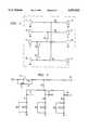
- FIG. 1is an exploded perspective view of a panel in accordance with an embodiment of the invention
- FIGS. 2-5are schematic circuit diagrams of various portions of the panel illustrated in FIG. 1;
- FIGS. 6-9are schematic side views of a pair of panels such as shown in FIG. 1 illustrating the connection of the panels to telecommunications equipment.
- the jack panel 10includes a front surface 11 with a plurality of apertures, 12-20, therein.
- the panelhas two side walls, 21 and 22. In between the two side walls, 21 and 22, are a mylar sheet 23 and a printed circuit board 24.
- the circuit boardincludes on a front edge a set of jacks, 25-28, which are aligned with respective apertures (12, 13 and 18, 19) in the panel front surface and are capable of receiving standard plugs (not shown) therein.
- the jacksare in the form of standard BNC coaxial connectors.
- a light emitting diode (LED) 29which protrudes through an aperture 20 in the front surface
- another LED 30which protrudes through another aperture 17 in the front surface
- a bantam jack 31which also protrudes through a respective aperture 14 in the front surface.
- a pair of buttons, 32 and 33are also mounted on the front edge of the board and protrude through corresponding apertures 15 and 16 in the front surface. These buttons are conventional type push button switches.
- the back edge of the circuit board 24also includes a set of plug-receiving jacks, 34-37, which protrude through apertures in the back surface of the panel (not shown).
- a set of electrical pins, 38is also provided on the back edge of the board for connection to a power source (not shown).
- the various elements on the board 24are electrically connected by conductive paths (not shown) formed on the surface of the board by standard techniques.
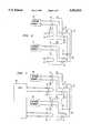
- FIG. 2is a schematic diagram showing the electrical interconnection of the various jacks.
- the position of jacks 34, 35, 25 and 26has been changed for purposes of clarity in the schematic.
- jacks 36 and 37are electrically coupled through switches RL1 and RL2 to corresponding jacks 34 and 35.
- the switches RL1 and RL2are latching relays, but other switching means can be employed.
- Jacks 27 and 28, which comprise the monitor ports of the panel,are resistively coupled to jacks 36 and 37, respectively.
- Switches RL3 and RL4, in the "through mode,”are connected together and floating.
- switches RL1 and RL2are thrown so that jacks 36 and 37 are electrically coupled to jacks 25 and 26, respectively.
- switches RL3 and RL4are thrown so that jacks 34 and 35 are now electrically connected to provide a loop-back path for any equipment coupled to these jacks.
- jacks 25-28 and 34-37are of a type which receive a plug without re-muting any of the electrical paths in the panel.
- switches RL1, RL2, RL3 and RL4require activation circuits to change the switch positions. Such activation circuits are illustrated in FIGS. 3 and 4.
- button 32bridges terminals 40 and 41 when depressed.
- Terminal 40is coupled to a power supply through one of pins 38 of FIG. 1, and to one plate of a capacitor C 1 .
- Terminal 41is coupled to a resistor R 1 which, in rum, is coupled to the other plate of capacitor C 1 .
- R 1 and C 1therefore, serve the function of arc suppression.
- Terminal 41is also coupled to terminal 42 which, in rum, is coupled to the bantam jack 31 of FIG. 1.
- Terminal 41is further coupled to the anode of a diode, D 1 , whose cathode is coupled to one end of each of three resistors R 7 , R 8 , and R 9 .
- the same end of resistors R 7 , R 8 and R 9is coupled to one plate of respective capacitors C 3 , C 4 and C 5 .
- the other plate of each capacitor C 3 , C 4 and C 5is coupled to ground.
- the other end of each of resistors R 7 , R.sub. 8 and R 9is coupled to one end of respective relay coils RLC1, RLC2 and RLC3.
- RLC1is positioned to throw switches RL1 and RL3 of FIG. 2, while RLC2 is positioned to throw switches RL2 and RL4 of FIG. 2.
- Coil RLC3is positioned to throw switch RL5 of FIG. 5 which operates the patch indicator (LED 30).
- Diodes D 3 , D 4 and D 5are coupled in parallel with coils RLC1, RLC2
- FIG. 4is essentially the same circuit configuration as FIG. 3 except that button 33 activates relays RLC4, RLC5 and RLC6.
- Relay RLC4is positioned to throw switches RL1 and RL3 back to their original positions (FIG. 2) when button 33 is depressed, and relay RLC5 is positioned to also throw switches RL2 and RL4 back to their original positions when button 33 is depressed.
- relay RLC6will throw switch RL5 to deactivate LED 30.
- FIGS. 6-9illustrate how a typical in-service cutover procedure can be performed between two panels, 10 and 50, with many features on the front panel omitted for the sake of clarity.
- a first network element 60is coupled to jacks 36 and 37, while a second network element 61 is coupled to corresponding jacks 56 and 57 of panel 50.
- These network elementscan be, for example, fiber optic terminals.
- a three-pronged jumper cable, including wires 62, 63 and 64,is connected by means of a three-pronged plug to jacks 25, 26 and 31, respectively.
- the plug at the opposite end of the wiresis inserted into corresponding jacks of panel 50 so that output jack 26 of panel 10 is coupled to input jack 53 of panel 50, and input jack 25 of panel 10 is coupled to output jack 52 of panel 50.
- bantam jack 31 of panel 10is coupled to bantam jack 51 of panel 50.
- network element 60is electrically coupled to network element 61 through the wires 62 and 63.
- Wire 64electrically connects the button 32 of panel 10 to the activation circuit of panel 50 through terminal 42 (see FIG. 3) so that only one button needs to be depressed to throw all the switches of both panels.
- the yellow LEDs on both panelswill also light to indicate a patching mode.
- DACSdigital access cross-connect
- the DACS machine 65can then be programmed to provide the appropriate mapping to achieve the desired cross-connect between panels 10 and 50.
- the button 33(of FIG. 4) is depressed to throw the switches in both panels 10 and 50, to electrically connect jack 37 to jack 35 and jack 36 to jack 34 in panel 10, and jack 57 to jack 55 and jack 56 to jack 54 in panel 50.
- Thisconnects the network elements 60 and 61 through the DACS machine 65.
- Wires 62, 63 and 64now shown in phantom, no longer provide electrical connection and can be removed or kept in place in the event of a breakdown of the DACS machine.
- interconnect panelWhile the present invention has been described primarily in the context of an interconnect panel, it should be appreciated that the invention is equally applicable for a rear cross-connect panel.
- Such panelsmay substitute the BNC connectors (34-37) coupled to digital equipment with wire-wrapped terminals or with 440-type jacks having built-in switches. Consequently, it should be understood that, in the context of this application, the term “connector” is intended to be broad enough to include any type of electrical connection, while the term “jack” is intended to include only connectors which are capable of receiving an electrical plug therein.
Landscapes
- Engineering & Computer Science (AREA)
- Computer Networks & Wireless Communication (AREA)
- Structure Of Telephone Exchanges (AREA)
Abstract
Description
Claims (6)
Priority Applications (1)
| Application Number | Priority Date | Filing Date | Title |
|---|---|---|---|
| US08/250,253US5552962A (en) | 1994-05-27 | 1994-05-27 | Interconnect and cross-connect equipment including jack panel |
Applications Claiming Priority (1)
| Application Number | Priority Date | Filing Date | Title |
|---|---|---|---|
| US08/250,253US5552962A (en) | 1994-05-27 | 1994-05-27 | Interconnect and cross-connect equipment including jack panel |
Publications (1)
| Publication Number | Publication Date |
|---|---|
| US5552962Atrue US5552962A (en) | 1996-09-03 |
Family
ID=22946975
Family Applications (1)
| Application Number | Title | Priority Date | Filing Date |
|---|---|---|---|
| US08/250,253Expired - LifetimeUS5552962A (en) | 1994-05-27 | 1994-05-27 | Interconnect and cross-connect equipment including jack panel |
Country Status (1)
| Country | Link |
|---|---|
| US (1) | US5552962A (en) |
Cited By (31)
| Publication number | Priority date | Publication date | Assignee | Title |
|---|---|---|---|---|
| US5685741A (en)* | 1996-06-27 | 1997-11-11 | Adc Telecommunications, Inc. | On demand plug-in jack card and monitor frame |
| US5997311A (en)* | 1998-04-24 | 1999-12-07 | Lucent Technologies Inc. | Interconnect and cross-connect equipment panel for telecommunications apparatus |
| US6046913A (en)* | 1998-04-24 | 2000-04-04 | Lucent Technologies Inc. | Panel mounted power module with adaptor mounting bracket |
| US6078507A (en)* | 1997-09-29 | 2000-06-20 | Tronolone; James | Patch panel with incorporated distribution amplifiers |
| US6146167A (en)* | 1998-09-16 | 2000-11-14 | Telect, Inc. | Telecommunication module having edge mounted jack and switch therefor |
| US6241562B1 (en)* | 1999-06-22 | 2001-06-05 | Avaya Technology Corp. | Digital cross connect/interconnect module |
| WO2002082585A3 (en)* | 2001-04-06 | 2003-02-13 | Adc Telecommunications Inc | Electronic signal transmission and switching jack |
| US6535367B1 (en) | 2000-06-13 | 2003-03-18 | Bittree Incorporated | Electrical patching system |
| US6554652B1 (en) | 2002-02-15 | 2003-04-29 | Adc Telecommunications, Inc. | Jack assembly including baluns interface; and methods |
| US6587354B1 (en) | 1998-09-18 | 2003-07-01 | Duane B. Kutsch | Telecommunication assembly |
| US6632106B2 (en) | 2001-07-24 | 2003-10-14 | Adc Telecommunications, Inc. | Jack; jack assembly; and methods |
| US20040077220A1 (en)* | 2002-10-21 | 2004-04-22 | Bruce Musolf | High density patching system |
| US20040097138A1 (en)* | 2002-11-18 | 2004-05-20 | Kha Thong Binh | Modular cross-connect with removable switch assembly |
| US20040151173A1 (en)* | 2003-02-05 | 2004-08-05 | Alcatel | Electrical signal regenerator |
| US20040190684A1 (en)* | 2003-03-28 | 2004-09-30 | Urban Blake R. | Electronic looping systems and methods for telecommunications system central offices |
| US20040223311A1 (en)* | 2002-05-31 | 2004-11-11 | Jay Lee | RF circuit modules and integrated chassis with power interface for RF circuit modules |
| US6838884B1 (en) | 2001-05-22 | 2005-01-04 | Worldcom, Inc. | Timing output panel |
| US20050026506A1 (en)* | 2002-11-18 | 2005-02-03 | Trompeter Electronics, Inc. | Modular cross-connect with hot-swappable modules |
| US20050176275A1 (en)* | 2004-02-05 | 2005-08-11 | Panamax | Modular signal and power connection device |
| US20060010494A1 (en)* | 2002-08-08 | 2006-01-12 | Olivier Emsellem | Mechanical device for connection and disconnection between a data input and a data output |
| US20070211883A1 (en)* | 2006-03-07 | 2007-09-13 | Jorg Franzke | Telecommunications device having distribution units arranged in block configuration |
| US20070211642A1 (en)* | 2006-03-07 | 2007-09-13 | Jorg Franzke | Telecommunication distribution device with multi-circuit board arrangement |
| US20070211740A1 (en)* | 2006-03-07 | 2007-09-13 | Jorg Franzke | Telecommunications distribution system with line sharing |
| US20070211882A1 (en)* | 2006-03-07 | 2007-09-13 | Francois Hatte | Control method for a telecommunication distribution system |
| US7393249B2 (en) | 2006-04-21 | 2008-07-01 | Trompeter Electronics, Inc. | Interconnection and monitoring module |
| US20080266049A1 (en)* | 2005-05-18 | 2008-10-30 | Adc Gmbh | Active Distribution Device in a Subscriber Connection Area |
| US20090129568A1 (en)* | 2005-05-18 | 2009-05-21 | Adc Gmbh | Distribution device in a subscriber connection area |
| US7912019B1 (en) | 2001-07-02 | 2011-03-22 | Haw-Minn Lu | Applications of upgradeable scalable switching networks |
| US7929522B1 (en)* | 2001-07-02 | 2011-04-19 | Haw-Minn Lu | Systems and methods for upgrading scalable switching networks |
| US20110122648A1 (en)* | 2009-11-24 | 2011-05-26 | Telect, Inc. | High density digital signal cross-connect system |
| US8391282B1 (en) | 2001-07-02 | 2013-03-05 | Haw-Minn Lu | Systems and methods for overlaid switching networks |
Citations (13)
| Publication number | Priority date | Publication date | Assignee | Title |
|---|---|---|---|---|
| US3509297A (en)* | 1968-07-15 | 1970-04-28 | Bell Telephone Labor Inc | Test connector |
| US3869582A (en)* | 1973-06-04 | 1975-03-04 | Allstate Insurance Co | Intrabuilding telephone system |
| US4096359A (en)* | 1976-10-12 | 1978-06-20 | International Standard Electric Corporation | Key telephone system interconnection apparatus |
| US4237352A (en)* | 1979-04-06 | 1980-12-02 | T-Bar Incorporated | Patch module for connecting to off-line transmission lines of a switchably selected pair of transmission lines |
| US4476357A (en)* | 1982-09-28 | 1984-10-09 | T-Bar Incorporated | Switching apparatus employing conductor contracts on a movable elastomeric member |
| US4618194A (en)* | 1985-07-15 | 1986-10-21 | At&T Bell Laboratories | Connecting block for digital system cross-connect frame |
| US4705921A (en)* | 1986-08-26 | 1987-11-10 | Vir, Inc. | Patch module |
| US4815104A (en)* | 1988-01-11 | 1989-03-21 | Telect, Inc. | Digital telecommunications network, cross-connect module |
| US5127851A (en)* | 1991-07-25 | 1992-07-07 | Reliance Comm/Tec Corporation | Modular patch panel |
| US5199878A (en)* | 1990-11-15 | 1993-04-06 | Adc Telecommunications, Inc. | Plug-in jack card for normally closed contacts |
| US5233501A (en)* | 1992-02-27 | 1993-08-03 | Telect, Inc. | Digital telecommunication network cross-connect module having a printed circuit board connected to jack switches |
| US5265156A (en)* | 1991-08-21 | 1993-11-23 | Augat Communication Products Inc. | Digital signal cross-connect panel |
| US5439395A (en)* | 1993-08-30 | 1995-08-08 | At&T Corp. | DSX jack |
- 1994
- 1994-05-27USUS08/250,253patent/US5552962A/ennot_activeExpired - Lifetime
Patent Citations (15)
| Publication number | Priority date | Publication date | Assignee | Title |
|---|---|---|---|---|
| US3509297A (en)* | 1968-07-15 | 1970-04-28 | Bell Telephone Labor Inc | Test connector |
| US3869582A (en)* | 1973-06-04 | 1975-03-04 | Allstate Insurance Co | Intrabuilding telephone system |
| US4096359A (en)* | 1976-10-12 | 1978-06-20 | International Standard Electric Corporation | Key telephone system interconnection apparatus |
| US4237352A (en)* | 1979-04-06 | 1980-12-02 | T-Bar Incorporated | Patch module for connecting to off-line transmission lines of a switchably selected pair of transmission lines |
| US4476357A (en)* | 1982-09-28 | 1984-10-09 | T-Bar Incorporated | Switching apparatus employing conductor contracts on a movable elastomeric member |
| US4618194A (en)* | 1985-07-15 | 1986-10-21 | At&T Bell Laboratories | Connecting block for digital system cross-connect frame |
| US4705921A (en)* | 1986-08-26 | 1987-11-10 | Vir, Inc. | Patch module |
| US4705921B1 (en)* | 1986-08-26 | 1992-12-08 | Vir Inc | |
| US4815104A (en)* | 1988-01-11 | 1989-03-21 | Telect, Inc. | Digital telecommunications network, cross-connect module |
| US4815104B1 (en)* | 1988-01-11 | 1991-07-02 | Telect Inc | |
| US5199878A (en)* | 1990-11-15 | 1993-04-06 | Adc Telecommunications, Inc. | Plug-in jack card for normally closed contacts |
| US5127851A (en)* | 1991-07-25 | 1992-07-07 | Reliance Comm/Tec Corporation | Modular patch panel |
| US5265156A (en)* | 1991-08-21 | 1993-11-23 | Augat Communication Products Inc. | Digital signal cross-connect panel |
| US5233501A (en)* | 1992-02-27 | 1993-08-03 | Telect, Inc. | Digital telecommunication network cross-connect module having a printed circuit board connected to jack switches |
| US5439395A (en)* | 1993-08-30 | 1995-08-08 | At&T Corp. | DSX jack |
Cited By (49)
| Publication number | Priority date | Publication date | Assignee | Title |
|---|---|---|---|---|
| US5685741A (en)* | 1996-06-27 | 1997-11-11 | Adc Telecommunications, Inc. | On demand plug-in jack card and monitor frame |
| US6078507A (en)* | 1997-09-29 | 2000-06-20 | Tronolone; James | Patch panel with incorporated distribution amplifiers |
| US5997311A (en)* | 1998-04-24 | 1999-12-07 | Lucent Technologies Inc. | Interconnect and cross-connect equipment panel for telecommunications apparatus |
| US6046913A (en)* | 1998-04-24 | 2000-04-04 | Lucent Technologies Inc. | Panel mounted power module with adaptor mounting bracket |
| US6146167A (en)* | 1998-09-16 | 2000-11-14 | Telect, Inc. | Telecommunication module having edge mounted jack and switch therefor |
| US6587354B1 (en) | 1998-09-18 | 2003-07-01 | Duane B. Kutsch | Telecommunication assembly |
| US20050233640A1 (en)* | 1998-09-18 | 2005-10-20 | Kutsch Duane B | Module-less cross connect assembly |
| US6241562B1 (en)* | 1999-06-22 | 2001-06-05 | Avaya Technology Corp. | Digital cross connect/interconnect module |
| US6535367B1 (en) | 2000-06-13 | 2003-03-18 | Bittree Incorporated | Electrical patching system |
| US7092176B2 (en) | 2001-04-06 | 2006-08-15 | Adc Telecommunications, Inc. | Electronic signal transmission and switching jack |
| US20090223799A1 (en)* | 2001-04-06 | 2009-09-10 | Adc Telecommunications, Inc. | Electronic signal transmission and switching jack |
| WO2002082585A3 (en)* | 2001-04-06 | 2003-02-13 | Adc Telecommunications Inc | Electronic signal transmission and switching jack |
| US7495188B2 (en) | 2001-04-06 | 2009-02-24 | Adc Telecommunications, Inc. | Electronic signal transmission and switching jack |
| US6992257B2 (en) | 2001-04-06 | 2006-01-31 | Adc Telecommunications, Inc. | Electronic signal transmission and switching jack |
| US7968810B2 (en) | 2001-04-06 | 2011-06-28 | Adc Telecommunications, Inc. | Electronic signal transmission and switching jack |
| US20070199809A1 (en)* | 2001-04-06 | 2007-08-30 | Adc Telecommunications, Inc. | Electronic signal transmission and switching jack |
| US6838884B1 (en) | 2001-05-22 | 2005-01-04 | Worldcom, Inc. | Timing output panel |
| US7929522B1 (en)* | 2001-07-02 | 2011-04-19 | Haw-Minn Lu | Systems and methods for upgrading scalable switching networks |
| US7912019B1 (en) | 2001-07-02 | 2011-03-22 | Haw-Minn Lu | Applications of upgradeable scalable switching networks |
| US8391282B1 (en) | 2001-07-02 | 2013-03-05 | Haw-Minn Lu | Systems and methods for overlaid switching networks |
| US6632106B2 (en) | 2001-07-24 | 2003-10-14 | Adc Telecommunications, Inc. | Jack; jack assembly; and methods |
| US6554652B1 (en) | 2002-02-15 | 2003-04-29 | Adc Telecommunications, Inc. | Jack assembly including baluns interface; and methods |
| US20040223311A1 (en)* | 2002-05-31 | 2004-11-11 | Jay Lee | RF circuit modules and integrated chassis with power interface for RF circuit modules |
| US6842348B2 (en) | 2002-05-31 | 2005-01-11 | Pci Technologies, Inc. | RF circuit modules and integrated chassis with power interface for RF circuit modules |
| US7855896B2 (en) | 2002-05-31 | 2010-12-21 | Jay Lee | RF circuit modules and integrated chassis with power interface for RF circuit modules |
| US20060010494A1 (en)* | 2002-08-08 | 2006-01-12 | Olivier Emsellem | Mechanical device for connection and disconnection between a data input and a data output |
| WO2004039091A3 (en)* | 2002-10-21 | 2004-09-30 | Adc Telecommunications Inc | High density patching system |
| US6875060B2 (en) | 2002-10-21 | 2005-04-05 | Adc Telecommunications, Inc. | High density patching system |
| US20040077220A1 (en)* | 2002-10-21 | 2004-04-22 | Bruce Musolf | High density patching system |
| US20050026506A1 (en)* | 2002-11-18 | 2005-02-03 | Trompeter Electronics, Inc. | Modular cross-connect with hot-swappable modules |
| US6752665B2 (en) | 2002-11-18 | 2004-06-22 | Trompeter Electronics, Inc. | Modular cross-connect with removable switch assembly |
| US20040097138A1 (en)* | 2002-11-18 | 2004-05-20 | Kha Thong Binh | Modular cross-connect with removable switch assembly |
| US20040151173A1 (en)* | 2003-02-05 | 2004-08-05 | Alcatel | Electrical signal regenerator |
| US7440512B2 (en)* | 2003-02-05 | 2008-10-21 | Alcatel | Electrical signal regenerator |
| US7177395B2 (en)* | 2003-03-28 | 2007-02-13 | Bellsouth Intellectual Property Corporation | Electronic looping systems for telecommunications system central offices |
| US20040190684A1 (en)* | 2003-03-28 | 2004-09-30 | Urban Blake R. | Electronic looping systems and methods for telecommunications system central offices |
| US6979205B2 (en)* | 2004-02-05 | 2005-12-27 | Panamax | Modular signal and power connection device |
| US20050176275A1 (en)* | 2004-02-05 | 2005-08-11 | Panamax | Modular signal and power connection device |
| US20080266049A1 (en)* | 2005-05-18 | 2008-10-30 | Adc Gmbh | Active Distribution Device in a Subscriber Connection Area |
| US20090129568A1 (en)* | 2005-05-18 | 2009-05-21 | Adc Gmbh | Distribution device in a subscriber connection area |
| US8582585B2 (en) | 2005-05-18 | 2013-11-12 | Adc Gmbh | Distribution device in a subscriber connection area |
| US20070211882A1 (en)* | 2006-03-07 | 2007-09-13 | Francois Hatte | Control method for a telecommunication distribution system |
| US20070211740A1 (en)* | 2006-03-07 | 2007-09-13 | Jorg Franzke | Telecommunications distribution system with line sharing |
| US20070211642A1 (en)* | 2006-03-07 | 2007-09-13 | Jorg Franzke | Telecommunication distribution device with multi-circuit board arrangement |
| US20070211883A1 (en)* | 2006-03-07 | 2007-09-13 | Jorg Franzke | Telecommunications device having distribution units arranged in block configuration |
| US8437344B2 (en) | 2006-03-07 | 2013-05-07 | Adc Telecommunications, Inc. | Telecommunication distribution device with multi-circuit board arrangement |
| US7393249B2 (en) | 2006-04-21 | 2008-07-01 | Trompeter Electronics, Inc. | Interconnection and monitoring module |
| US20110122648A1 (en)* | 2009-11-24 | 2011-05-26 | Telect, Inc. | High density digital signal cross-connect system |
| US8760875B2 (en) | 2009-11-24 | 2014-06-24 | Telect, Inc. | High density digital signal cross-connect system |
Similar Documents
| Publication | Publication Date | Title |
|---|---|---|
| US5552962A (en) | Interconnect and cross-connect equipment including jack panel | |
| US8708724B2 (en) | Patch cord insertion detection and light illumination capabilities | |
| US7217152B1 (en) | Patch panel with tracer | |
| US5233501A (en) | Digital telecommunication network cross-connect module having a printed circuit board connected to jack switches | |
| CA1316233C (en) | Digital telecommunications network, cross-connect module | |
| US6632106B2 (en) | Jack; jack assembly; and methods | |
| US5546282A (en) | Telecommunication network digital cross-connect panels having insertable modules with printed circuit board mounted coaxial jack switches | |
| US5582525A (en) | Drop and insert card | |
| WO1995001665A1 (en) | Rear cross connect dsx system | |
| EP1410647A2 (en) | Jack module | |
| CA2548707C (en) | Tracer lamp arrangement | |
| US5438617A (en) | Low frequency digital network cross-connect panel | |
| US5265156A (en) | Digital signal cross-connect panel | |
| GB2206248A (en) | Telephone line test receptacle | |
| US20040235356A1 (en) | Cross-connector for interfacing multiple communication devices | |
| CA2572768C (en) | Long frame high density patching system | |
| US7127042B2 (en) | Device for providing dual monitoring of digital equipment | |
| AU604576B2 (en) | Terminal block comprising a plurality of block components | |
| US6215856B1 (en) | Dual mode monitor module | |
| AU648439B2 (en) | Digital cross-connect assembly | |
| US7238035B2 (en) | Normal-through jack with monitor and test ports | |
| US4338496A (en) | Testing facility for telephone conference bridge | |
| US20020084787A1 (en) | Self powered DSL port continuity checker |
Legal Events
| Date | Code | Title | Description |
|---|---|---|---|
| AS | Assignment | Owner name:AT&T CORP., NEW YORK Free format text:ASSIGNMENT OF ASSIGNORS INTEREST;ASSIGNORS:FEUSTEL, CLAY ALLISON;SCAGLIONE, JOHN MARIO;REEL/FRAME:007021/0728;SIGNING DATES FROM 19940516 TO 19940518 | |
| AS | Assignment | Owner name:AT&T IPM CORP., FLORIDA Free format text:ASSIGNMENT OF ASSIGNORS INTEREST;ASSIGNOR:AT&T CORP.;REEL/FRAME:007467/0511 Effective date:19950428 | |
| STCF | Information on status: patent grant | Free format text:PATENTED CASE | |
| FEPP | Fee payment procedure | Free format text:PAYOR NUMBER ASSIGNED (ORIGINAL EVENT CODE: ASPN); ENTITY STATUS OF PATENT OWNER: LARGE ENTITY | |
| FPAY | Fee payment | Year of fee payment:4 | |
| AS | Assignment | Owner name:THE CHASE MANHATTAN BANK, AS COLLATERAL AGENT, TEX Free format text:CONDITIONAL ASSIGNMENT OF AND SECURITY INTEREST IN PATENT RIGHTS;ASSIGNOR:LUCENT TECHNOLOGIES INC. (DE CORPORATION);REEL/FRAME:011722/0048 Effective date:20010222 | |
| FPAY | Fee payment | Year of fee payment:8 | |
| AS | Assignment | Owner name:LUCENT TECHNOLOGIES INC., NEW JERSEY Free format text:TERMINATION AND RELEASE OF SECURITY INTEREST IN PATENT RIGHTS;ASSIGNOR:JPMORGAN CHASE BANK, N.A. (FORMERLY KNOWN AS THE CHASE MANHATTAN BANK), AS ADMINISTRATIVE AGENT;REEL/FRAME:018584/0446 Effective date:20061130 | |
| FPAY | Fee payment | Year of fee payment:12 |