US5551984A - Vertical heat treatment apparatus with a circulation gas passage - Google Patents
Vertical heat treatment apparatus with a circulation gas passageDownload PDFInfo
- Publication number
- US5551984A US5551984AUS08/353,288US35328894AUS5551984AUS 5551984 AUS5551984 AUS 5551984AUS 35328894 AUS35328894 AUS 35328894AUS 5551984 AUS5551984 AUS 5551984A
- Authority
- US
- United States
- Prior art keywords
- transfer chamber
- heat treatment
- gas
- opening
- treatment apparatus
- Prior art date
- Legal status (The legal status is an assumption and is not a legal conclusion. Google has not performed a legal analysis and makes no representation as to the accuracy of the status listed.)
- Expired - Lifetime
Links
Images


Classifications
- H—ELECTRICITY
- H01—ELECTRIC ELEMENTS
- H01L—SEMICONDUCTOR DEVICES NOT COVERED BY CLASS H10
- H01L21/00—Processes or apparatus adapted for the manufacture or treatment of semiconductor or solid state devices or of parts thereof
- H01L21/02—Manufacture or treatment of semiconductor devices or of parts thereof
- H01L21/04—Manufacture or treatment of semiconductor devices or of parts thereof the devices having potential barriers, e.g. a PN junction, depletion layer or carrier concentration layer
- H01L21/18—Manufacture or treatment of semiconductor devices or of parts thereof the devices having potential barriers, e.g. a PN junction, depletion layer or carrier concentration layer the devices having semiconductor bodies comprising elements of Group IV of the Periodic Table or AIIIBV compounds with or without impurities, e.g. doping materials
- H01L21/26—Bombardment with radiation
- H—ELECTRICITY
- H01—ELECTRIC ELEMENTS
- H01L—SEMICONDUCTOR DEVICES NOT COVERED BY CLASS H10
- H01L21/00—Processes or apparatus adapted for the manufacture or treatment of semiconductor or solid state devices or of parts thereof
- H01L21/67—Apparatus specially adapted for handling semiconductor or electric solid state devices during manufacture or treatment thereof; Apparatus specially adapted for handling wafers during manufacture or treatment of semiconductor or electric solid state devices or components ; Apparatus not specifically provided for elsewhere
- H01L21/677—Apparatus specially adapted for handling semiconductor or electric solid state devices during manufacture or treatment thereof; Apparatus specially adapted for handling wafers during manufacture or treatment of semiconductor or electric solid state devices or components ; Apparatus not specifically provided for elsewhere for conveying, e.g. between different workstations
- H01L21/67739—Apparatus specially adapted for handling semiconductor or electric solid state devices during manufacture or treatment thereof; Apparatus specially adapted for handling wafers during manufacture or treatment of semiconductor or electric solid state devices or components ; Apparatus not specifically provided for elsewhere for conveying, e.g. between different workstations into and out of processing chamber
- H01L21/67757—Apparatus specially adapted for handling semiconductor or electric solid state devices during manufacture or treatment thereof; Apparatus specially adapted for handling wafers during manufacture or treatment of semiconductor or electric solid state devices or components ; Apparatus not specifically provided for elsewhere for conveying, e.g. between different workstations into and out of processing chamber vertical transfer of a batch of workpieces
- C—CHEMISTRY; METALLURGY
- C23—COATING METALLIC MATERIAL; COATING MATERIAL WITH METALLIC MATERIAL; CHEMICAL SURFACE TREATMENT; DIFFUSION TREATMENT OF METALLIC MATERIAL; COATING BY VACUUM EVAPORATION, BY SPUTTERING, BY ION IMPLANTATION OR BY CHEMICAL VAPOUR DEPOSITION, IN GENERAL; INHIBITING CORROSION OF METALLIC MATERIAL OR INCRUSTATION IN GENERAL
- C23C—COATING METALLIC MATERIAL; COATING MATERIAL WITH METALLIC MATERIAL; SURFACE TREATMENT OF METALLIC MATERIAL BY DIFFUSION INTO THE SURFACE, BY CHEMICAL CONVERSION OR SUBSTITUTION; COATING BY VACUUM EVAPORATION, BY SPUTTERING, BY ION IMPLANTATION OR BY CHEMICAL VAPOUR DEPOSITION, IN GENERAL
- C23C16/00—Chemical coating by decomposition of gaseous compounds, without leaving reaction products of surface material in the coating, i.e. chemical vapour deposition [CVD] processes
- C23C16/44—Chemical coating by decomposition of gaseous compounds, without leaving reaction products of surface material in the coating, i.e. chemical vapour deposition [CVD] processes characterised by the method of coating
- C23C16/4401—Means for minimising impurities, e.g. dust, moisture or residual gas, in the reaction chamber
- C—CHEMISTRY; METALLURGY
- C23—COATING METALLIC MATERIAL; COATING MATERIAL WITH METALLIC MATERIAL; CHEMICAL SURFACE TREATMENT; DIFFUSION TREATMENT OF METALLIC MATERIAL; COATING BY VACUUM EVAPORATION, BY SPUTTERING, BY ION IMPLANTATION OR BY CHEMICAL VAPOUR DEPOSITION, IN GENERAL; INHIBITING CORROSION OF METALLIC MATERIAL OR INCRUSTATION IN GENERAL
- C23C—COATING METALLIC MATERIAL; COATING MATERIAL WITH METALLIC MATERIAL; SURFACE TREATMENT OF METALLIC MATERIAL BY DIFFUSION INTO THE SURFACE, BY CHEMICAL CONVERSION OR SUBSTITUTION; COATING BY VACUUM EVAPORATION, BY SPUTTERING, BY ION IMPLANTATION OR BY CHEMICAL VAPOUR DEPOSITION, IN GENERAL
- C23C16/00—Chemical coating by decomposition of gaseous compounds, without leaving reaction products of surface material in the coating, i.e. chemical vapour deposition [CVD] processes
- C23C16/44—Chemical coating by decomposition of gaseous compounds, without leaving reaction products of surface material in the coating, i.e. chemical vapour deposition [CVD] processes characterised by the method of coating
- C23C16/54—Apparatus specially adapted for continuous coating
- Y—GENERAL TAGGING OF NEW TECHNOLOGICAL DEVELOPMENTS; GENERAL TAGGING OF CROSS-SECTIONAL TECHNOLOGIES SPANNING OVER SEVERAL SECTIONS OF THE IPC; TECHNICAL SUBJECTS COVERED BY FORMER USPC CROSS-REFERENCE ART COLLECTIONS [XRACs] AND DIGESTS
- Y10—TECHNICAL SUBJECTS COVERED BY FORMER USPC
- Y10S—TECHNICAL SUBJECTS COVERED BY FORMER USPC CROSS-REFERENCE ART COLLECTIONS [XRACs] AND DIGESTS
- Y10S414/00—Material or article handling
- Y10S414/135—Associated with semiconductor wafer handling
- Y10S414/139—Associated with semiconductor wafer handling including wafer charging or discharging means for vacuum chamber
- Y—GENERAL TAGGING OF NEW TECHNOLOGICAL DEVELOPMENTS; GENERAL TAGGING OF CROSS-SECTIONAL TECHNOLOGIES SPANNING OVER SEVERAL SECTIONS OF THE IPC; TECHNICAL SUBJECTS COVERED BY FORMER USPC CROSS-REFERENCE ART COLLECTIONS [XRACs] AND DIGESTS
- Y10—TECHNICAL SUBJECTS COVERED BY FORMER USPC
- Y10S—TECHNICAL SUBJECTS COVERED BY FORMER USPC CROSS-REFERENCE ART COLLECTIONS [XRACs] AND DIGESTS
- Y10S414/00—Material or article handling
- Y10S414/135—Associated with semiconductor wafer handling
- Y10S414/14—Wafer cassette transporting
Definitions
- a semiconductor fabrication processincludes heat treatment steps, such as film deposition, oxidation, diffusion etc.
- heat treatment stepssuch as film deposition, oxidation, diffusion etc.
- a vertical heat treatment apparatuswhich has the advantage of taking in little air during operation.
- this conventional heat treating apparatusincludes a transfer chamber 12 which is an operation space formed below a vertical heat treatment furnace 11, and a wafer boat 13 which is vertically moved between the transfer chamber 12 and the heat treatment furnace by boat elevator 14.
- Semiconductor wafers Ware mounted on the wafer boat 13 vertically spaced from each other to be carried on the wafer boat 13 into the heat treatment furnace 11 for a heat treatment there. After the heat treatment, the wafer boat 13 is loaded out of the heat treatment furnace 11 to dismount the wafers W from the wafer boat 13.
- the filter unit 15comprises a filter material folded in a bellows which is secured to a frame at the top and bottom and at both sides by an adhesive or seal member. Since the wafers unloaded out of the heat treatment furnace have high temperatures, radiant heat from the wafers W heats the filter unit 15 up to high temperatures, and organic components, e.g., hydrocarbon, etc., are scattered from the adhesive, e.g., resin used in the filter unit 15. The organic components react with films deposited on the heated semiconductor wafers W to adversely deteriorate electric characteristics, film performance of the deposited film, etc., with a result of lower yields of the wafers. This is much affective to micronization of wafers for above 16 MDRM.
- ULPAUltra Low Penetration Air
- Conventionally ULPA filter of this kindare made of borosilicate glass fiber as a filter material, which is based on SiO 2 , B 2 O 3 , etc.
- the filter material of the conventional ULPA filtersis borosilicate glass fiber based on SiO 2 , B 2 O 3 , etc.
- the filter material itselfis exposed to bad conditions, such as exposure to acid components used in wafer washing and quartz washing and to radiant heat from the wafer boat and reaction tube immediately after a heat treatment, boron (B) is generated. Consequently there has been a risk that the boron (8) may mix into clean air which has passed the filter material.
- the filter material of this kindis generally folded in the bellows of an accordion which is secured to a suitable frame.
- Adhesives and spacers for securing the filter materialare made from resins containing volatile solvents. There is a risk that in the above-mentioned acid atmosphere or high-temperature atmosphere, organic gas may be generated from these adhesives and spacers themselves and contaminate the clean air which has passed through the filter.
- the conventional heat treatment apparatushas a risk that boron and organic components generated from the filter itself stay on the surfaces of wafers and contaminate the wafers, with a result of low yields.
- An object of the present inventionis to provide a heat treatment apparatus which can reduce the amount of impurities that attach to objects to be treated in the transfer chamber.
- the heat treatment apparatusin which objects to be treated on an objects-to-be-treated holder are loaded from a transfer chamber into a reaction vessel, and unloaded therefrom, and gas in the transfer chamber is ventilated through a circulation passage having a drawing port and a blowout port opened in the transfer chamber.
- the heat treatment apparatusfurther includes dust removing filter units, a clean gas source, a supply passage for supplying clean gas from the clean gas source into the transfer chamber without passing the clean gas through the dust removing filter units, an opening/closing valve provided in the supply passage, and a control unit for selecting a first mode or a second mode.
- the first modeinvolves opening the opening/closing valve and stopping ventilation through the circulation gas passage
- the secondinvolves closing the opening/closing valve and effecting ventilation through the circulation gas passage.
- gas circulationis stopped through the circulation gas passage from, e.g., the unloading of the treated objects to the loading of the objects to be next treated, and clean gas is fed in the transfer chamber without passing through the dust removing filter units to form gas flows.
- the gasis circulated between the circulation gas passage and the transfer chamber to form gas flows of the gas from the dust removing filters, whereby particles in the transfer chamber are removed. Accordingly even when the dust removing filter units are exposed to radiant heat from the heat-treated objects, the amount of organic components from the filter units that attach to the objects to be treated can be much suppressed.
- the present inventionuses, as a filter material of the filter units of the heat treatment apparatus and a resin supporting the filter material, materials which generate no boron and organic components.
- the heat treatment apparatuscomprises a heat treatment furnace for heating objects to be treated to make a required heat treatment, a casing for housing a heat treatment furnace, blowing means for forming air flows in the casing, and a filter unit for cleaning the air flows and establishing clean environments for the apparatus, a material of the filter unit being PTFE (polytetrafluoroethylene).
- PTFEpolytetrafluoroethylene
- FIG. 1is a vertical sectional view of the heat treatment apparatus according to a first embodiment of the present invention.
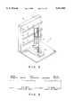
- FIG. 2is a perspective view of the general structure of the heat treatment apparatus of FIG. 1.
- FIG. 3is a perspective of a major part of the heat treatment apparatus FIG. 1.
- FIG. 4is a view explaining relationships between the treatment steps of the heat treatment apparatus according to the first embodiment and gas flow forming modes.
- FIG. 5is a vertical sectional view of a modification of the heat treatment apparatus according to the first embodiment of FIG. 1.
- FIG. 6is a view explaining relationships between the treatment steps of the heat treatment apparatus according to the first embodiment and gas flow forming modes.
- FIG. 7is a partially broken perspective view of a filter unit used in the heat treatment apparatus according to a second embodiment of the present invention.
- FIG. 8is a partial enlarged top view of a filter of the filter unit of FIG. 7.
- FIG. 9is a diagrammatical vertical sectional view of the heat treatment apparatus according to the second embodiment.
- FIG. 10is a flow chart of the procedure of a method for evaluating the effect of the heat treatment apparatus according to the second embodiment.
- FIG. 11is a graph comparing contamination of wafers treated by the heat treatment apparatus according to the second embodiment with that of wafers treated by the use of the conventional ULPA filter.
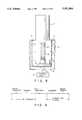
- FIG. 12is a perspective view of the appearance of the heat treatment apparatus according to the second embodiment of the present invention.
- FIG. 13is a view explaining direction of air flows in the casing of the heat treatment apparatus according to the second embodiment of the present invention.
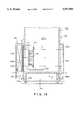
- FIG. 14is a partial vertical sectional view of the structure of the lower space of the interior of the casing of the heat treatment apparatus according to the second embodiment of the present invention.
- FIG. 15is a partial vertical sectional view of the structure of the second blowing means of the heat treatment apparatus according to the second embodiment of the present invention.
- FIG. 16is a diagrammatic view of the conventional heat treatment apparatus.
- FIG. 1is a vertical sectional side view of the vertical heat treatment apparatus according to a first embodiment of the present invention.
- FIG. 2is a perspective view of the general structure of the vertical heat treatment apparatus of FIG. 1.
- reference numeral 2indicates a vertical heat treatment apparatus.
- the interior of the vertical heat treatment apparatus 2is not shown but includes a reaction tube, a heater provided around the reaction tube, etc.
- a transfer chamber 3, an operational space,is formed below the heat treatment furnace 2, and the heat treatment furnace 2 and the transfer chamber 3 are surrounded by a casing 20.
- a boat elevator 31which is a lift mechanism for a wafer boat 32 is provided in the transfer chamber 3.
- a wafer boat for holding objects to be treated (wafers)is provided on the boat elevator 31.
- the wafer boat 32holds wafers W vertically spaced from each other and is loaded into and unloaded out of the reaction tube of the heat treatment furnace.
- a wafer carrier (hereinafter called “carrier”) mount 21where wafers are delivered/received is provided on the front side of the carrier mount 21 through a transfer territory of a carrier transfer mechanism 22.
- the wafer transfer mechanism 22is provided between the carrier mount 21 and the boat elevator 31, and a carrier stocker 24 is disposed above the carrier mount 21. Ventilation holes through which air is, respectively, drawn and blown out are formed in both side walls of the transfer chamber 3.
- An air flow restricting platee.g., a metal plate with a number of fine holes 41, is provided in the ventilation hole on the air drawing side.
- a circulation passage 4 as a circulation air flueis formed on both sides and the underside of the transfer chamber 3.
- a shutter Swhich is opened/closed by an opening/closing mechanism 42 to open/close the circulation passage 4 and blowing means, e.g., a first blowing fan 43, are provided, and a dust removing filter unit S in the form of, e.g., a bellows of a filter material, is provided in the blowout port of the duct 4.
- An exhaust duct 44is branched from the circulation passage 4 upstream of the first blowing fan 43 and is connected on the discharge side to a factory exhaust duct.
- a second blowing fan 45is disposed in the exhaust duct 44.
- air feed pipes 60, 61, 62are provided on an upper end part, the middle part and a lower end part of the front side of the dust removing filter unit 5 horizontally widthwise of the dust removing filter unit S.
- a number of air blowout holes 6are formed lengthwise in the sides of the respective air feed pipes opposed to the wafer boat 32.
- the air feed pipes 60-62are feed pipes for clean air and, as shown in FIG. 1, are connected to a common clean air source 64, e.g., a clean air bomb.
- control unit 7which controls the switching of modes of ventilation for the transfer chamber 3.
- the control unit 7controls the opening/closing mechanism 42 for the shutter S, the first blowing fan 43, the second blowing fan 45 and an opening/closing valve 63 for switching, at a set timing, between a first mode of circulating clean air from the clean air source 64 into the transfer chamber 3 and discharging the air through the exhaust duct 44, and a second mode of circulating air in the transfer chamber 3 through the circulation passage 4.
- Carrier or cassette C holding 25 sheets of objects to be treated, e.g., wafers,is placed on the carrier entry/exit port 23 by convey means (not shown), and the carrier C is transferred onto the carrier mount 21 by the carrier transfer mechanism 22. Then, in the transfer chamber 3, the wafers W are transferred from the carrier C on the carrier mount 21 to the wafer boat 32.
- the wafer boat 32can hold, e.g., 100 sheets of wafers W vertically spaced from each other.
- the boat elevator 31is lifted to load the wafer boat 32 from the transfer chamber 3 into the heat treatment furnace 2.
- the heat treatment furnace 2which has been preheated up to, e.g., about 800° C., is further heated up to a required temperature, e.g., above 1000° C., after the wafers W have been loaded, and a heat treatment, e.g, oxidation, is conducted.
- the boat elevator 31is lowered to unload the wafer boat 32 into the transfer chamber 3, and the transfer mechanism 22 takes out the wafers W from the wafer boat 32 to transfer them into the carrier C on the carrier mount 21.
- the control unit 7selects the second mode, i.e., the air circulation mode in the step of transferring the wafers onto the wafer boat 32, the step of loading the wafers and the step of a heat treatment.
- the second modewith the first blowing fan 43 on, second blowing fan 45 off, the opening/closing valve 63 closed and the shutter S opened, air in the transfer chamber 3 is drawn from the air flow restriction plate 41 into a part of the circulation passage 4 on the right side of the transfer chamber 3 as viewed in FIG. 1 and is circulated into a part of the circulation passage 4 on the left side of the transfer chamber 3 as viewed in FIG.
- the control unit 7selects from this time to the end of dismount of the wafers W from the wafer boat 32 the first mode, i.e., the clean air supply mode.
- the first modei.e., the clean air supply mode.
- clean air from the clean air source 64is sent to the air feed pipes 60-62 and is fed into the transfer chamber 3 through the blowout holes 6 by, e.g., 200 1/minute.
- the airenters a space (a part of the circulation passage 4) behind the air flow restricting plate 41 through the same 41 and is exhausted through the exhaust duct 44 by the second blowing fan 45.
- clean airis fed from the clean air source 64 into the transfer chamber 3 without being passed through the dust removing filter unit 5 with air flow through the circulation passage 4 stopped, whereby even when wafers W are unloaded, and the dust removing filter unit 5 is heated up to considerably high temperatures by radiant heat from the unloaded high temperature wafers W, scattering of impurities, such as boron from the filter material of the dust removing filter unit 5 and organic components from the adhesive into the transfer chamber 3 can be prevented while particles generated in the transfer chamber can be discharged. Consequently attachment of particles and impurities to the wafers W can be prevented. Then, after the wafers W have been dismounted from the wafer boat 32, air is circulated through the circulation. Thus the clean air source 64 is actuated only when necessary, which can reduce costs.
- the air circulation modesmay be selected when wafers W are transferred or loaded other than in the above-described steps.
- FIGS. 5 and 6show an embodiment of such a case.
- a control unit 8turns on the blowing fan 43 during the steps of transferring wafers onto the wafer boat 32, loading the wafer boat 32 and conducting a heat treatment, and during the steps of unloading the wafer boat 32 and dismounting the wafers from the wafer boat 32 the blowing fan 43 is turned off.
- the dust removing filter unit 5is heated by radiant heat of the wafers W, no air flows through the dust removing filter unit 5, and accordingly contamination from scattering boron and organic components from the dust removing filter 5a can be depressed.
- the wafers Ware thus less likely to be made defective.
- air feed pipesmay be provided, e.g., on the back of the apparatus depicted in of FIG. 2.
- the gas streams in the transfer chamber 3are not limited to air flows, and, for example, it is possible that the transfer chamber 3 is in the form of a load-lock chamber, and the gas streams are nitrogen gas streams.
- the heat treatment apparatus according to the first embodimentis applicable to not only oxidation, but also to batch heat treatments, such as diffusion, CVD, etching, etc.
- FIG. 7shows a filter unit 101 used in the second embodiment.
- the filter unit 101has the same structure as the conventional generally used ULPA filters.
- a filter 102 of the filter unit 101has pleats (bellows) of a filter material 103.
- the filter material 103is an unwoven fabric of PTFE (polytetrafluoroethylene) or an olefin-based fiber, and has a 0.05-0.22 ⁇ m fiber diameter and a 0.3 ⁇ m bore.
- the pleats of the filter material 103is set by a spacer 104 in the form of a plastic band adhered to a side of the filter material 103 (FIG. 8).
- the spacer 104is made of high molecular dimer acid polyamide resin.
- the molten resinis adhered to a side of the filter material 103 when the filter material 103 is pleated, and then cool-set, whereby a gap G of, e.g., about 5 mm is formed between respective pleats of the filter material 103.
- the filter 102(e.g., 600 cm-square) is secured to an aluminium frame 105.
- the filter 102is fixed at the ends by an end seal material 106 of epoxy resin and at the sides by a side seal material 107 of a chloroprene-based adhesive.
- Gaskets 108are formed of chloroprene sponge and support the ends of the filter material 103.
- This filter unit 101is provided in a test heat treatment apparatus 111 whose front view is shown in FIG. 9.
- This test heat treatment apparatus 111includes a blower 113, a wafer holder 114 to be exposed to downflows caused by the blower 113 in a stainless steel casing 112, and further a first damper 115, a second damper 116 and a third damper 117 lower in the casing 112.
- the first and the third dampers 115, 117are closed, and the second damper 116 is opened, whereby a circulation flow as shown is formed in the casing 112.
- the downflow caused by the blower 113flows through an area isolated from a space (reaction space) with the wafer holder 114 provided in by a partition plate 118 and into an upper part of the casing 112, and then passes through a heater 119 and is again formed into a downflow by the blower 113.
- the filter unit 101 of FIG. 7is provided between the blower 113 and the wafer holder 114 to clean the flow from the blower 113.
- the test heat treatment apparatushas this structure.
- test treatment apparatuswith a dummy wafer DW set on the wafer holder 114 was actually operated. Contamination of the dummy wafer DW will be explained.
- the dummy wafer DWhad a 1000 ⁇ -thickness SiO 2 film formed on a silicon wafer by wet oxidation. Following this film deposition, the dummy wafer DW was cleaned for 10 minutes by the so-called SPM (Sulfuric acid Hydrogen Peroxide Mix), i.e., the dummy wafer DW was cleaned for 10 minutes with a cleaning liquid of 110° C. which was a mixture of sulphuric acid (H2SO4) and hydrogen peroxide (H202) by 4:1, then further cleaned for 102 minutes with pure water, and then dried by a spin drier.
- SPMsulfuric acid Hydrogen Peroxide Mix
- the heat treatment apparatuswas idled continuously for 6 weeks in the state for forming the so-called one-way flow in the casing 112 with the second damper 116 closed, and the first and the third dampers 115, 117 open.
- the dummy wafer DWwas set on the wafer holder 114, and as shown in FIG. 9 the first and the third dampers 115, 117 are closed, the second damper 116 is opened so that circulating flows was formed in the casing 112.
- the dummy wafer DWwas left in this state, and contamination of the wafer surface was measured by the so-called contact angle gauging method respectively after 3, 6, 9 and 12 hours. This test procedure is shown in the flow chart of FIG. 10.
- a heater 119 in FIG. 9was heated up to a circulation temperature of 40° C., a flow rate through the filter unit 101 was 0.35 m/sec, and a distance between the filter unit 101 and the dummy wafer DW was 50 mm.
- the filter unit 101 having the filter 105 made of the above mentioned filter material 103 of borosilicate glass fiber based on SiO 2 , B 2 O 3 , etc.was additionally prepared.
- the contaminationwas evaluated under the same conditions by the contact angle gauging method.
- This heat treatment apparatus 111is fabricated for test use but can produce substantially the same environments as the general heat treatment apparatuses. Even in a case that the filter unit 101 is applied to the general heat treatment apparatuses, the corresponding effect, i.e., no organic impurities are generated from the filter unit, and accordingly a suppression of the contamination of the wafer surfaces can be easily assured.
- the heat treatment apparatus 121includes a cylindrical heat treatment vessel (furnace) 122 having the upper end closed and the lower end opened, and lift means 124 which is disposed below the heat treatment vessel 122 to support and move a wafer boat 123 into and out of the heat treatment vessel 122.
- the wafer boat 123horizontally holds 100 sheets of wafers W, objects to be treated, vertically spaced from each other.
- the wafer boat 123is loaded into and unloaded out of the heat treatment vessel 122 on the lift means 124.
- the heat treatment apparatus 121includes transfer means, e.g., wafer transfer means 125 for transferring the wafers W between cassettes C holding wafers W, and the wafer boat 123.
- transfer meanse.g., wafer transfer means 125 for transferring the wafers W between cassettes C holding wafers W, and the wafer boat 123.
- the heat treatment vessel 122, the wafer boat 123 and the lift means 124are provided in a casing 126.
- the casing 126has an opening 127 in the front side which is opened and closed by a door (not shown).
- the cassettes Care conveyed into and out of the casing through the opening 127.
- the I/O port 131Inside the opening 127, an I/O port 131 on which two cassettes C are placed is provided. At the r/O port 131, as will be explained later, air flows which flow downward from above are formed in the casing.
- the I/O port 131includes alignment means (not shown) for aligning orientation flats of the wafers W in the cassettes C, and horizontal-vertical repositioning means (not shown) for turning the cassettes C by 90° to reposition the wafers W from a horizontal state to a vertical state. After the wafers W in the cassettes C are aligned at the orientation flats, the cassettes holding the wafers W are repositioned so as to be horizontal.
- a carrier transfer means 132is provided inwardly of the I/O port 131 so that the cassettes C are transferred onto carrier stage 133 arranged in shelves positioned inwardly of the carrier transfer means 132.
- the carrier stage 133can hold, e.g., 8 cassettes C which store wafers W to be treated and treated wafers W.
- a transfer stage 134is provided below the carrier stage 133.
- the cassettes Care transferred between the carrier stage 133 and the transfer stage 134 through the carrier transfer means 132.
- a wafer transfer means 125transfers wafers W between the cassettes C on the transfer stage 134 and the wafer boat 123 on the lift means 124.
- the heat treatment apparatus 121has first blowing means 141 and also a single door for maintenance formed in one side of a treatment space 126a in the casing 126, i.e., in an opening 126b in the left side thereof.
- the first blowing means 141includes a fan 142 which is disposed below an opening 141a and draws air through the opening 141a and blows the air, a first filter unit 143 which removes particles, etc. in the air fed by the fan 142 into the casing 126 through a duct 141b, and an equalizing plate 144 provided inwardly of the first filter unit 143 with a gap ⁇ parallel therewith.
- the first filter unit 143has quite the same structure as the filter unit 101 of FIG. 7 and uses as the filter material an unwoven fabric of PTFE or an olefin based fiber.
- the equalizing plate 144has a number of blowout holes 144a. Supplied air which has passed the first filter unit 143 is uniformly blown from the entire surface of the equalizing plate 144 to a side duct 145 in a side opening 126c opposed to the equalizing plate 144.
- the side duct 145is in communication with an opening 145b formed therebelow through a bottom duct 146 provided on the bottom of the casing 126.
- air blown by the first blowing means 141is circulated in the sequence of through space 126a, through opening 126c of the side duct 145, through the bottom duct 146 the first blowing means 141 to form a circulating air flows X, and the circulating flows X is cleaned by the first filter unit 143 while flowing in the sequence.
- the bottom duct 146accommodates control means for driving the lift means 124, the wafer transfer means 125, etc., and its lines, etc.
- Active carbon filters 147, 148are provided respectively in the entrance of the bottom duct 145 and the exit thereof, i.e., on the inside of an opening 145b and that of an opening 141a.
- the active carbon filters 147, 148are in the form of, e.g., gas permeable mats of active carbon, or sheets of active carbon with a number of distributed fine holes, and function as the so-called prefilter for the first filter unit 143.
- a slit 145ais formed in the side behind the side duct 145 for passing air from the first blowing means 141.
- a part of the circulating air flows Xis exhausted as exhaust EA outside the casing 126 through the slit 145a as shown in FIG. 13.
- air supply SAin an amount corresponding to the exhaust EA is taken into the casing 126 from a clean room chamber (not shown).
- An active carbon filter 171is provided also in the air inlet 126d as shown in FIG. 13, so that the air supply SA to be introduced through the air inlet 126d can have organic impurities removed before supplied.
- second blowing means 151is provided along the back side of the carrier stage 133 and below the air inlet 126d.
- the second blowing means 151includes a vessel 152 with a slit 152a opposed to the air inlet 126d, a fan 153 which takes in air from the clean room through the slit 152a and the air inlet 126d and blows the air to the carrier stage 133, an active carbon filter 154 for cleaning the blown air, and second filter unit 155.
- the second filter unit 155uses as the filter material unwoven fabric of PTF and olefine-based fiber as does the first filter unit 143. The air which has passed the second filter means 155 clean is blown onto the wafers W in the cassettes C on the carrier stage 133 to form air flows Y in FIG.13.
- slits 152bare formed respectively in both sides of the vessel 152 of the second blowing means 151.
- the slits 152bdraw air flows Y1 which have impinged on the front of the casing 126 and returned and send the air to the active carbon filter 154 and the second filter unit 155 for again cleaning the air.
- a third blowing means 161is provided downstream of the air flows Y and above the I/O port 131. Most of the air flows Y is drawn by the third blowing means 161 and blown in descending air flows Z.
- the third blowing means 161has basically the same structure as the second blowing means 151, and has an active carbon filter at the upstream and, on a lower stage, a filter unit using as the filter material an unwoven fabric of PTFE or an olefin-based fiber.
- the heat treatment apparatus 121The operation of the heat treatment apparatus 121 according to the present embodiment will be explained.
- First the heat treatment vessel 122is heated up to a required temperature in accordance with a treatment to be made on objects to be treated, wafers W.
- the first blowing means 141, the second blowing means 151 and the third blowing means 161are actuated to form the circulating air flows X, the air flows Y and the descending air flows Z in the casing 126 as in FIG. 13.
- the cassettes C on the carrier stage 133are transferred onto the transfer stage 134 by the carrier transfer means 132.
- the wafers W in the cassettes Care mounted onto the wafer boat 123 by the wafer transfer means 125.
- the wafer boat 123is lifted by the lift means 124 to be loaded into the heat treatment vessel 122. The heat treatment is conducted there on the wafers W.
- the circulating air flows Xare formed by the first blowing means 141 in the casing 126. As shown in FIG. 14, this cleaned air flows are blown to the wafer boat 123. Accordingly even if particles should be generated when the wafers W are mounted on the wafer boat 123, they do not attach to the surface of the wafers W. There is therefore no risk that the particles may stay on the surfaces of the wafers W by flowing in the direction of the air flow.
- the circulating air flows Xhave been cleaned by the active carbon filters 147, 148 in the bottom duct 146, and the first filter unit 141, and the wafers W are free from the risk of contamination by exposure to the circulating air flows X.
- the first filter unit 141is made of an unwoven fabric of PTFE or an olefin-based fiber as the filter material, whose effect was confirmed in the above described embodiment. Even in environments where radiant heat from the heat treatment vessel 122 is present, the filter material is very stable, and does not generate organic impurities, such as hydrocarbon.
- the air flowshave organic impurities removed by the active carbon filters 147, 148, and can stably function for a very long period of time.
- the air flows Y and the descending air flows Z formed by the second blowing means 151 and the third blowing means 161are cleaned by the active carbon filter and the filter material of an unwoven fabric of PTFE or an olefin-based fiber, and can achieve the same effect as the circulating air flows X.
- the filter unit used in the present inventiondoes not basically differ from the conventional filter unit in appearance and constitution. Accordingly the filter unit of the present invention is readily applicable to heat treatment apparatuses in use by replacing their filter unit with the filter unit of the present invention or adding the active carbon filters. Thus the filter unit of the present invention is very practical.
Landscapes
- Chemical & Material Sciences (AREA)
- Engineering & Computer Science (AREA)
- Physics & Mathematics (AREA)
- Chemical Kinetics & Catalysis (AREA)
- Materials Engineering (AREA)
- Mechanical Engineering (AREA)
- Metallurgy (AREA)
- Organic Chemistry (AREA)
- General Chemical & Material Sciences (AREA)
- Manufacturing & Machinery (AREA)
- General Physics & Mathematics (AREA)
- Condensed Matter Physics & Semiconductors (AREA)
- Computer Hardware Design (AREA)
- Microelectronics & Electronic Packaging (AREA)
- Power Engineering (AREA)
- Health & Medical Sciences (AREA)
- High Energy & Nuclear Physics (AREA)
- Toxicology (AREA)
- Container, Conveyance, Adherence, Positioning, Of Wafer (AREA)
Abstract
Description
Claims (11)
Applications Claiming Priority (4)
| Application Number | Priority Date | Filing Date | Title |
|---|---|---|---|
| JP34142593AJP3402713B2 (en) | 1993-12-10 | 1993-12-10 | Heat treatment equipment |
| JP5-341425 | 1993-12-10 | ||
| JP6037889AJPH07226382A (en) | 1994-02-10 | 1994-02-10 | Heat treatment device |
| JP6-037889 | 1994-02-10 |
Publications (1)
| Publication Number | Publication Date |
|---|---|
| US5551984Atrue US5551984A (en) | 1996-09-03 |
Family
ID=26377048
Family Applications (1)
| Application Number | Title | Priority Date | Filing Date |
|---|---|---|---|
| US08/353,288Expired - LifetimeUS5551984A (en) | 1993-12-10 | 1994-12-05 | Vertical heat treatment apparatus with a circulation gas passage |
Country Status (3)
| Country | Link |
|---|---|
| US (1) | US5551984A (en) |
| KR (1) | KR100269413B1 (en) |
| TW (1) | TW273574B (en) |
Cited By (38)
| Publication number | Priority date | Publication date | Assignee | Title |
|---|---|---|---|---|
| US5735961A (en)* | 1995-05-25 | 1998-04-07 | Kokusai Electric Co., Ltd. | Semiconductor fabricating apparatus, method for controlling oxygen concentration within load-lock chamber and method for generating native oxide |
| US5863808A (en)* | 1995-08-30 | 1999-01-26 | Shin-Etsu Handotai Co., Ltd. | Method of storing and transporting wafers and method of determining the amount of organic materials attached to stored wafers |
| US5972116A (en)* | 1994-12-29 | 1999-10-26 | F.T.I. Co., Ltd. | Method and apparatus for producing a semiconductor device |
| US6036781A (en)* | 1996-04-04 | 2000-03-14 | Samsung Electronics Co., Ltd. | Apparatus for guiding air current in a wafer loading chamber for chemical vapor deposition equipment |
| US6224679B1 (en)* | 1997-08-12 | 2001-05-01 | Tokyo Electron Limited | Controlling gas in a multichamber processing system |
| US6270581B1 (en)* | 1997-02-12 | 2001-08-07 | Kokusai Electric Co., Ltd. | Wet-oxidation apparatus and wet-oxidation method |
| US6309438B1 (en)* | 1998-11-16 | 2001-10-30 | Mine Safety Appliances Company | Filter unit and dust-proof mask therewith |
| SG85106A1 (en)* | 1998-03-03 | 2001-12-19 | Canon Kk | Soi substrate and method and system for manufacturing the same |
| US20020078980A1 (en)* | 2000-12-25 | 2002-06-27 | Yuji Kamikawa | System for processing substrate with liquid |
| US6461437B1 (en)* | 2000-01-26 | 2002-10-08 | Mitsubishi Denki Kabushiki Kaisha | Apparatus used for fabricating liquid crystal device and method of fabricating the same |
| US20020151154A1 (en)* | 2001-03-16 | 2002-10-17 | Semiconductor Energy Laboratory Co. Ltd. | Heat treatment apparatus and heat treatment method |
| US20020164843A1 (en)* | 2001-03-16 | 2002-11-07 | Semiconductor Energy Laboratory Co., Ltd. | Method of manufacturing a semiconductor device |
| US20020197785A1 (en)* | 2001-03-16 | 2002-12-26 | Semiconductor Energy Laboratory Co. Ltd. | Process for manufacturing a semiconductor device |
| US20030037802A1 (en)* | 2001-07-23 | 2003-02-27 | Hitachi, Ltd. | Semiconductor treating apparatus and cleaning method of the same |
| US20050098107A1 (en)* | 2003-09-24 | 2005-05-12 | Du Bois Dale R. | Thermal processing system with cross-flow liner |
| US6913956B2 (en) | 2001-01-19 | 2005-07-05 | Semiconductor Energy Laboratory Co., Ltd. | Semiconductor device and method of manufacturing the same |
| EP1143047A4 (en)* | 1999-09-29 | 2006-08-23 | Shinetsu Handotai Kk | Wafer, epitaxial filter, and method of manufacture thereof |
| US7115453B2 (en) | 2001-01-29 | 2006-10-03 | Semiconductor Energy Laboratory Co., Ltd. | Semiconductor device and manufacturing method of the same |
| US7141822B2 (en) | 2001-02-09 | 2006-11-28 | Semiconductor Energy Laboratory Co., Ltd. | Semiconductor device and method for manufacturing the same |
| US7195990B2 (en) | 2001-01-30 | 2007-03-27 | Semiconductor Energy Laboratory Co., Ltd. | Process for producing a photoelectric conversion device that includes using a gettering process |
| US7202119B2 (en) | 2001-03-26 | 2007-04-10 | Semiconductor Energy Laboratory Co., Ltd. | Method of manufacturing semiconductor device |
| US20070134415A1 (en)* | 2005-12-01 | 2007-06-14 | Ki-Hyun Hwang | Oxidation Treatment Apparatus and Method |
| US20070298555A1 (en)* | 2001-02-16 | 2007-12-27 | Semiconductor Energy Laboratory Co., Ltd. | Method of manufacturing a semiconductor device |
| US7374976B2 (en) | 2002-11-22 | 2008-05-20 | Semiconductor Energy Laboratory Co., Ltd. | Method for fabricating thin film transistor |
| US20090130794A1 (en)* | 2006-04-20 | 2009-05-21 | Volker Probst | Thermal evaporation apparatus, use and method of depositing a material |
| CN102280363A (en)* | 2010-06-14 | 2011-12-14 | 株式会社日立国际电气 | Substrate processing apparatus |
| US8940082B2 (en) | 2009-11-30 | 2015-01-27 | Bsh Bosch Und Siemens Hausgeraete Gmbh | Filter element for an extractor hood and extractor hood |
| US20170008042A1 (en)* | 2015-07-09 | 2017-01-12 | Samsung Electronics Co., Ltd. | Furnace-type semiconductor apparatus, method of cleaning the same, and method of forming thin film using the same |
| US20170218513A1 (en)* | 2016-02-02 | 2017-08-03 | Hitachi Kokusai Electric Inc. | Substrate processing apparatus |
| US20180040488A1 (en)* | 2016-08-04 | 2018-02-08 | Hitachi Kokusai Electric Inc. | Substrate processing apparatus, recording medium, and fluid circulation mechanism |
| US20180105933A1 (en)* | 2015-04-21 | 2018-04-19 | Eugene Technology Co., Ltd. | Substrate processing apparatus and method for cleaning chamber |
| US10134578B2 (en)* | 2012-05-30 | 2018-11-20 | Tokyo Electron Limited | Housing and substrate processing apparatus including the same |
| US20190019705A1 (en)* | 2016-03-24 | 2019-01-17 | Kokusai Electric Corporation | Substrate processing apparatus, method of manufacturing semiconductor device, and recording medium |
| US10508336B2 (en) | 2015-01-21 | 2019-12-17 | Kokusai Electric Corporation | Substrate processing apparatus |
| CN111074237A (en)* | 2018-10-18 | 2020-04-28 | 君泰创新(北京)科技有限公司 | source bottle |
| US20220148893A1 (en)* | 2020-11-06 | 2022-05-12 | Tokyo Electron Limited | Heat treatment apparatus and dummy substrate processing method |
| US11579538B2 (en)* | 2020-01-06 | 2023-02-14 | Semes Co., Ltd. | Load port unit, storage apparatus including the same, and exhaust method |
| US11782404B2 (en) | 2014-11-25 | 2023-10-10 | Applied Materials, Inc. | Substrate processing systems, apparatus, and methods with substrate carrier and purge chamber environmental controls |
Families Citing this family (1)
| Publication number | Priority date | Publication date | Assignee | Title |
|---|---|---|---|---|
| KR101376739B1 (en) | 2012-06-22 | 2014-03-26 | (주) 예스티 | Heating and pressurization apparatus of improved cleanliness |
Citations (23)
| Publication number | Priority date | Publication date | Assignee | Title |
|---|---|---|---|---|
| US4612174A (en)* | 1983-11-24 | 1986-09-16 | Heinrich-Hertz-Institute fur Nachrichtentechnik Berlin GmbH | Method of removing noxious substances from gases |
| US4894071A (en)* | 1988-09-27 | 1990-01-16 | Tech Paper, Inc. | Portable air cleaner |
| JPH04196523A (en)* | 1990-11-28 | 1992-07-16 | Tokyo Electron Sagami Ltd | Heat treatment equipment |
| US5139459A (en)* | 1990-10-22 | 1992-08-18 | Tdk Corporation | Clean transfer method and system therefor |
| JPH04269824A (en)* | 1991-02-26 | 1992-09-25 | Tokyo Electron Sagami Ltd | Vertical type heat-treating device |
| JPH04269825A (en)* | 1991-02-26 | 1992-09-25 | Tokyo Electron Sagami Ltd | Vertical type heat-treating device |
| JPH04306824A (en)* | 1991-04-03 | 1992-10-29 | Tokyo Electron Sagami Ltd | Heat treatment device |
| US5181819A (en)* | 1990-10-09 | 1993-01-26 | Tokyo Electron Sagami Limited | Apparatus for processing semiconductors |
| US5219464A (en)* | 1990-10-09 | 1993-06-15 | Tokyo Electron Limited | Clean air apparatus |
| US5221201A (en)* | 1990-07-27 | 1993-06-22 | Tokyo Electron Sagami Limited | Vertical heat treatment apparatus |
| US5254170A (en)* | 1989-08-07 | 1993-10-19 | Asm Vt, Inc. | Enhanced vertical thermal reactor system |
| US5261935A (en)* | 1990-09-26 | 1993-11-16 | Tokyo Electron Sagami Limited | Clean air apparatus |
| US5261167A (en)* | 1990-09-27 | 1993-11-16 | Tokyo Electron Sagami Limited | Vertical heat treating apparatus |
| US5277579A (en)* | 1991-03-15 | 1994-01-11 | Tokyo Electron Sagami Limited | Wafers transferring method in vertical type heat treatment apparatus and the vertical type heat treatment apparatus provided with a wafers transferring system |
| US5303671A (en)* | 1992-02-07 | 1994-04-19 | Tokyo Electron Limited | System for continuously washing and film-forming a semiconductor wafer |
| US5320733A (en)* | 1990-12-21 | 1994-06-14 | Ultrakust Electronic Gmbh | Sensor system |
| US5328360A (en)* | 1991-04-03 | 1994-07-12 | Tokyo Election Sagami Kabushiki Kaisha | Heat-treating apparatus |
| US5378283A (en)* | 1992-12-04 | 1995-01-03 | Tokyo Electron Kabushiki Kaisha | Treating device |
| US5388944A (en)* | 1992-02-07 | 1995-02-14 | Tokyo Electron Tohoku Kabushiki Kaisha | Vertical heat-treating apparatus and heat-treating process by using the vertical heat-treating apparatus |
| US5433785A (en)* | 1992-10-14 | 1995-07-18 | Sony Corporation | Thermal treatment apparatus, semiconductor device fabrication apparatus, load-lock chamber |
| US5459943A (en)* | 1993-02-04 | 1995-10-24 | Tokyo Electron Limited | Air cleaning apparatus |
| US5462397A (en)* | 1993-03-16 | 1995-10-31 | Tokyo Electron Limited | Processing apparatus |
| US5464475A (en)* | 1994-05-20 | 1995-11-07 | Advanced Micro Devices, Inc. | Work-in-process storage pod |
- 1994
- 1994-12-02TWTW083111244Apatent/TW273574B/zhnot_activeIP Right Cessation
- 1994-12-05USUS08/353,288patent/US5551984A/ennot_activeExpired - Lifetime
- 1994-12-09KRKR1019940033374Apatent/KR100269413B1/ennot_activeExpired - Fee Related
Patent Citations (26)
| Publication number | Priority date | Publication date | Assignee | Title |
|---|---|---|---|---|
| US4612174A (en)* | 1983-11-24 | 1986-09-16 | Heinrich-Hertz-Institute fur Nachrichtentechnik Berlin GmbH | Method of removing noxious substances from gases |
| US4894071A (en)* | 1988-09-27 | 1990-01-16 | Tech Paper, Inc. | Portable air cleaner |
| US5254170A (en)* | 1989-08-07 | 1993-10-19 | Asm Vt, Inc. | Enhanced vertical thermal reactor system |
| US5336325A (en)* | 1989-08-07 | 1994-08-09 | Asm Vt, Inc. | Enhanced vertical thermal reactor system |
| US5221201A (en)* | 1990-07-27 | 1993-06-22 | Tokyo Electron Sagami Limited | Vertical heat treatment apparatus |
| US5261935A (en)* | 1990-09-26 | 1993-11-16 | Tokyo Electron Sagami Limited | Clean air apparatus |
| US5261167A (en)* | 1990-09-27 | 1993-11-16 | Tokyo Electron Sagami Limited | Vertical heat treating apparatus |
| US5181819A (en)* | 1990-10-09 | 1993-01-26 | Tokyo Electron Sagami Limited | Apparatus for processing semiconductors |
| US5219464A (en)* | 1990-10-09 | 1993-06-15 | Tokyo Electron Limited | Clean air apparatus |
| US5139459A (en)* | 1990-10-22 | 1992-08-18 | Tdk Corporation | Clean transfer method and system therefor |
| JPH04196523A (en)* | 1990-11-28 | 1992-07-16 | Tokyo Electron Sagami Ltd | Heat treatment equipment |
| US5320733A (en)* | 1990-12-21 | 1994-06-14 | Ultrakust Electronic Gmbh | Sensor system |
| JPH04269824A (en)* | 1991-02-26 | 1992-09-25 | Tokyo Electron Sagami Ltd | Vertical type heat-treating device |
| US5226812A (en)* | 1991-02-26 | 1993-07-13 | Tokyo Electron Sagami Kabushiki Kaisha | Vertical type heat-treating apparatus |
| US5207578A (en)* | 1991-02-26 | 1993-05-04 | Toyko Electron Sagami Limited | Heat processing apparatus of vertical type |
| JPH04269825A (en)* | 1991-02-26 | 1992-09-25 | Tokyo Electron Sagami Ltd | Vertical type heat-treating device |
| US5277579A (en)* | 1991-03-15 | 1994-01-11 | Tokyo Electron Sagami Limited | Wafers transferring method in vertical type heat treatment apparatus and the vertical type heat treatment apparatus provided with a wafers transferring system |
| JPH04306824A (en)* | 1991-04-03 | 1992-10-29 | Tokyo Electron Sagami Ltd | Heat treatment device |
| US5328360A (en)* | 1991-04-03 | 1994-07-12 | Tokyo Election Sagami Kabushiki Kaisha | Heat-treating apparatus |
| US5303671A (en)* | 1992-02-07 | 1994-04-19 | Tokyo Electron Limited | System for continuously washing and film-forming a semiconductor wafer |
| US5388944A (en)* | 1992-02-07 | 1995-02-14 | Tokyo Electron Tohoku Kabushiki Kaisha | Vertical heat-treating apparatus and heat-treating process by using the vertical heat-treating apparatus |
| US5433785A (en)* | 1992-10-14 | 1995-07-18 | Sony Corporation | Thermal treatment apparatus, semiconductor device fabrication apparatus, load-lock chamber |
| US5378283A (en)* | 1992-12-04 | 1995-01-03 | Tokyo Electron Kabushiki Kaisha | Treating device |
| US5459943A (en)* | 1993-02-04 | 1995-10-24 | Tokyo Electron Limited | Air cleaning apparatus |
| US5462397A (en)* | 1993-03-16 | 1995-10-31 | Tokyo Electron Limited | Processing apparatus |
| US5464475A (en)* | 1994-05-20 | 1995-11-07 | Advanced Micro Devices, Inc. | Work-in-process storage pod |
Non-Patent Citations (1)
| Title |
|---|
| Leonard, Milt, Expanded Teflon Filter Helps Build Denser Faster Disk Drives, Electronic Design, May 25, 1989 V. 37 No. 11 p. 30.* |
Cited By (67)
| Publication number | Priority date | Publication date | Assignee | Title |
|---|---|---|---|---|
| US6248672B1 (en) | 1994-12-29 | 2001-06-19 | F.T.L. Co., Ltd. | Method of producing a semiconductor device in a heating furnace having a reaction tube with a temperature-equalizing zone |
| US5972116A (en)* | 1994-12-29 | 1999-10-26 | F.T.I. Co., Ltd. | Method and apparatus for producing a semiconductor device |
| US5879415A (en)* | 1995-05-25 | 1999-03-09 | Kokusai Electric Co., Ltd. | Semiconductor fabricating apparatus, method for controlling oxygen concentration within load-lock chamber and method for generating native oxide |
| US5735961A (en)* | 1995-05-25 | 1998-04-07 | Kokusai Electric Co., Ltd. | Semiconductor fabricating apparatus, method for controlling oxygen concentration within load-lock chamber and method for generating native oxide |
| US5863808A (en)* | 1995-08-30 | 1999-01-26 | Shin-Etsu Handotai Co., Ltd. | Method of storing and transporting wafers and method of determining the amount of organic materials attached to stored wafers |
| US6036781A (en)* | 1996-04-04 | 2000-03-14 | Samsung Electronics Co., Ltd. | Apparatus for guiding air current in a wafer loading chamber for chemical vapor deposition equipment |
| US6270581B1 (en)* | 1997-02-12 | 2001-08-07 | Kokusai Electric Co., Ltd. | Wet-oxidation apparatus and wet-oxidation method |
| US6224679B1 (en)* | 1997-08-12 | 2001-05-01 | Tokyo Electron Limited | Controlling gas in a multichamber processing system |
| SG85106A1 (en)* | 1998-03-03 | 2001-12-19 | Canon Kk | Soi substrate and method and system for manufacturing the same |
| US6309438B1 (en)* | 1998-11-16 | 2001-10-30 | Mine Safety Appliances Company | Filter unit and dust-proof mask therewith |
| US9163327B2 (en) | 1999-09-29 | 2015-10-20 | Shin-Etsu Handotai Co., Ltd. | Silicon wafer and a silicon epitaxial wafer having a polycrystal silicon layer formed on a major surface including boron concentration of the polycrystal silicon layer being 1×10¹⁵ atom/cm3 or less |
| EP1143047A4 (en)* | 1999-09-29 | 2006-08-23 | Shinetsu Handotai Kk | Wafer, epitaxial filter, and method of manufacture thereof |
| US6461437B1 (en)* | 2000-01-26 | 2002-10-08 | Mitsubishi Denki Kabushiki Kaisha | Apparatus used for fabricating liquid crystal device and method of fabricating the same |
| US20020078980A1 (en)* | 2000-12-25 | 2002-06-27 | Yuji Kamikawa | System for processing substrate with liquid |
| US6792958B2 (en)* | 2000-12-25 | 2004-09-21 | Tokyo Electron Limited | System for processing substrate with liquid |
| US6913956B2 (en) | 2001-01-19 | 2005-07-05 | Semiconductor Energy Laboratory Co., Ltd. | Semiconductor device and method of manufacturing the same |
| US7198992B2 (en) | 2001-01-19 | 2007-04-03 | Semiconductor Energy Laboratory Co., Ltd. | Method of manufacturing a semiconductor device comprising doping steps using gate electrodes and resists as masks |
| US7501671B2 (en) | 2001-01-19 | 2009-03-10 | Semiconductor Energy Laboratory Co., Ltd. | Semiconductor device and method of manufacturing the same |
| US7115453B2 (en) | 2001-01-29 | 2006-10-03 | Semiconductor Energy Laboratory Co., Ltd. | Semiconductor device and manufacturing method of the same |
| US7534670B2 (en) | 2001-01-29 | 2009-05-19 | Semiconductor Energy Laboratory Co., Ltd. | Semiconductor device and manufacturing method of the same |
| US7195990B2 (en) | 2001-01-30 | 2007-03-27 | Semiconductor Energy Laboratory Co., Ltd. | Process for producing a photoelectric conversion device that includes using a gettering process |
| US7736960B2 (en) | 2001-01-30 | 2010-06-15 | Semiconductor Energy Laboratory Co., Ltd. | Process for producing a photoelectric conversion device |
| US7141822B2 (en) | 2001-02-09 | 2006-11-28 | Semiconductor Energy Laboratory Co., Ltd. | Semiconductor device and method for manufacturing the same |
| US7538011B2 (en) | 2001-02-16 | 2009-05-26 | Semiconductor Energy Laboratory Co., Ltd. | Method of manufacturing a semiconductor device |
| US20070298555A1 (en)* | 2001-02-16 | 2007-12-27 | Semiconductor Energy Laboratory Co., Ltd. | Method of manufacturing a semiconductor device |
| US20080210164A1 (en)* | 2001-03-16 | 2008-09-04 | Semiconductor Energy Laboratory Co., Ltd. | Heat treatment apparatus and heat treatment method |
| US7122450B2 (en) | 2001-03-16 | 2006-10-17 | Semiconductor Energy Laboratory Co., Ltd. | Process for manufacturing a semiconductor device |
| US20020151154A1 (en)* | 2001-03-16 | 2002-10-17 | Semiconductor Energy Laboratory Co. Ltd. | Heat treatment apparatus and heat treatment method |
| US7118780B2 (en)* | 2001-03-16 | 2006-10-10 | Semiconductor Energy Laboratory Co., Ltd. | Heat treatment method |
| US20110262117A1 (en)* | 2001-03-16 | 2011-10-27 | Semiconductor Energy Laboratory Co., Ltd. | Heat Treatment Apparatus and Heat Treatment Method |
| US7052943B2 (en) | 2001-03-16 | 2006-05-30 | Semiconductor Energy Laboratory Co., Ltd. | Method of manufacturing a semiconductor device |
| US7485553B2 (en) | 2001-03-16 | 2009-02-03 | Semiconductor Energy Laboratory Co., Ltd. | Process for manufacturing a semiconductor device |
| US9666458B2 (en)* | 2001-03-16 | 2017-05-30 | Semiconductor Energy Laboratory Co., Ltd. | Heat treatment apparatus and heat treatment method |
| US20020197785A1 (en)* | 2001-03-16 | 2002-12-26 | Semiconductor Energy Laboratory Co. Ltd. | Process for manufacturing a semiconductor device |
| US7974524B2 (en) | 2001-03-16 | 2011-07-05 | Semiconductor Energy Laboratory Co., Ltd. | Heat treatment apparatus and heat treatment method |
| US20020164843A1 (en)* | 2001-03-16 | 2002-11-07 | Semiconductor Energy Laboratory Co., Ltd. | Method of manufacturing a semiconductor device |
| US7202119B2 (en) | 2001-03-26 | 2007-04-10 | Semiconductor Energy Laboratory Co., Ltd. | Method of manufacturing semiconductor device |
| US20030037802A1 (en)* | 2001-07-23 | 2003-02-27 | Hitachi, Ltd. | Semiconductor treating apparatus and cleaning method of the same |
| US7374976B2 (en) | 2002-11-22 | 2008-05-20 | Semiconductor Energy Laboratory Co., Ltd. | Method for fabricating thin film transistor |
| US20050098107A1 (en)* | 2003-09-24 | 2005-05-12 | Du Bois Dale R. | Thermal processing system with cross-flow liner |
| US20070134415A1 (en)* | 2005-12-01 | 2007-06-14 | Ki-Hyun Hwang | Oxidation Treatment Apparatus and Method |
| US8082878B2 (en)* | 2006-04-20 | 2011-12-27 | Saint-Gobain Glass France | Thermal evaporation apparatus, use and method of depositing a material |
| US8336489B2 (en)* | 2006-04-20 | 2012-12-25 | Volker Probst | Thermal evaporation apparatus, use and method of depositing a material |
| US20090130794A1 (en)* | 2006-04-20 | 2009-05-21 | Volker Probst | Thermal evaporation apparatus, use and method of depositing a material |
| US8940082B2 (en) | 2009-11-30 | 2015-01-27 | Bsh Bosch Und Siemens Hausgeraete Gmbh | Filter element for an extractor hood and extractor hood |
| US9698037B2 (en) | 2010-06-14 | 2017-07-04 | Hitachi Kokusai Electric Inc. | Substrate processing apparatus |
| CN102280363A (en)* | 2010-06-14 | 2011-12-14 | 株式会社日立国际电气 | Substrate processing apparatus |
| CN102280363B (en)* | 2010-06-14 | 2014-10-29 | 株式会社日立国际电气 | Substrate processing apparatus |
| US10134578B2 (en)* | 2012-05-30 | 2018-11-20 | Tokyo Electron Limited | Housing and substrate processing apparatus including the same |
| US11782404B2 (en) | 2014-11-25 | 2023-10-10 | Applied Materials, Inc. | Substrate processing systems, apparatus, and methods with substrate carrier and purge chamber environmental controls |
| US11512392B2 (en) | 2015-01-21 | 2022-11-29 | Kokusai Electric Corporation | Substrate processing apparatus |
| US12123091B2 (en) | 2015-01-21 | 2024-10-22 | Kokusai Electric Corporation | Substrate processing apparatus and method of manufacturing semiconductor device |
| US10508336B2 (en) | 2015-01-21 | 2019-12-17 | Kokusai Electric Corporation | Substrate processing apparatus |
| US20180105933A1 (en)* | 2015-04-21 | 2018-04-19 | Eugene Technology Co., Ltd. | Substrate processing apparatus and method for cleaning chamber |
| US20170008042A1 (en)* | 2015-07-09 | 2017-01-12 | Samsung Electronics Co., Ltd. | Furnace-type semiconductor apparatus, method of cleaning the same, and method of forming thin film using the same |
| US10413946B2 (en)* | 2015-07-09 | 2019-09-17 | Samsung Electronics Co., Ltd. | Furnace-type semiconductor apparatus, method of cleaning the same, and method of forming thin film using the same |
| US10550468B2 (en)* | 2016-02-02 | 2020-02-04 | Kokusai Electric Corporation | Substrate processing apparatus |
| US20170218513A1 (en)* | 2016-02-02 | 2017-08-03 | Hitachi Kokusai Electric Inc. | Substrate processing apparatus |
| US11124873B2 (en) | 2016-02-02 | 2021-09-21 | Kokusai Electric Corporation | Substrate processing apparatus |
| US10529605B2 (en)* | 2016-03-24 | 2020-01-07 | Kokusai Electric Corporation | Substrate processing apparatus, method of manufacturing semiconductor device, and recording medium |
| US20190019705A1 (en)* | 2016-03-24 | 2019-01-17 | Kokusai Electric Corporation | Substrate processing apparatus, method of manufacturing semiconductor device, and recording medium |
| US11694907B2 (en)* | 2016-08-04 | 2023-07-04 | Kokusai Electric Corporation | Substrate processing apparatus, recording medium, and fluid circulation mechanism |
| US20180040488A1 (en)* | 2016-08-04 | 2018-02-08 | Hitachi Kokusai Electric Inc. | Substrate processing apparatus, recording medium, and fluid circulation mechanism |
| CN111074237A (en)* | 2018-10-18 | 2020-04-28 | 君泰创新(北京)科技有限公司 | source bottle |
| US11579538B2 (en)* | 2020-01-06 | 2023-02-14 | Semes Co., Ltd. | Load port unit, storage apparatus including the same, and exhaust method |
| US20220148893A1 (en)* | 2020-11-06 | 2022-05-12 | Tokyo Electron Limited | Heat treatment apparatus and dummy substrate processing method |
| US12027384B2 (en)* | 2020-11-06 | 2024-07-02 | Tokyo Electron Limited | Heat treatment apparatus and dummy substrate processing method |
Also Published As
| Publication number | Publication date |
|---|---|
| TW273574B (en) | 1996-04-01 |
| KR950021004A (en) | 1995-07-26 |
| KR100269413B1 (en) | 2000-11-01 |
Similar Documents
| Publication | Publication Date | Title |
|---|---|---|
| US5551984A (en) | Vertical heat treatment apparatus with a circulation gas passage | |
| US5261935A (en) | Clean air apparatus | |
| KR102535776B1 (en) | High Flow Rate, Gas-Purge, Side Storage Pod Apparatus, Assemblies, and Methods | |
| US5447294A (en) | Vertical type heat treatment system | |
| US5261167A (en) | Vertical heat treating apparatus | |
| US6368411B2 (en) | Molecular contamination control system | |
| JP2021525954A (en) | Method using heating of substrate manufacturing equipment and factory interface chamber | |
| US5219464A (en) | Clean air apparatus | |
| US20120083120A1 (en) | Substrate processing apparatus and method of manufacturing a semiconductor device | |
| TW202130400A (en) | Substrate processing apparatus and methods with factory interface chamber filter purge | |
| JPH02138473A (en) | Treating device and treating method | |
| US5207578A (en) | Heat processing apparatus of vertical type | |
| JP4498362B2 (en) | Substrate processing apparatus and semiconductor device manufacturing method | |
| KR102289650B1 (en) | Apparatus for reducing moisture of front opening unified pod in load port module and semiconductor process device comprising the same | |
| US5413527A (en) | Environmental control apparatus | |
| US5514196A (en) | Air cleaning apparatus | |
| US5459943A (en) | Air cleaning apparatus | |
| JP2015146348A (en) | EFEM system | |
| JPH06224144A (en) | Processing apparatus | |
| JP3176160B2 (en) | Processing equipment | |
| JP2005183638A (en) | Substrate heat treatment apparatus | |
| US7935185B2 (en) | Film forming system and film forming method | |
| JP3402713B2 (en) | Heat treatment equipment | |
| JP3330169B2 (en) | Vertical heat treatment equipment with gas shower nozzle | |
| US4981436A (en) | Vertical type heat-treatment apparatus |
Legal Events
| Date | Code | Title | Description |
|---|---|---|---|
| AS | Assignment | Owner name:TOKYO ELECTRON KABUSHIKI KAISHA (A CORP. OF JAPAN Free format text:ASSIGNMENT OF ASSIGNORS INTEREST;ASSIGNOR:TANAHASHI, TAKASHI;REEL/FRAME:007259/0504 Effective date:19941129 Owner name:TOKYO ELECTRON TOHOKU KABUSHIKI KAISHA (A CORP. Free format text:ASSIGNMENT OF ASSIGNORS INTEREST;ASSIGNOR:TANAHASHI, TAKASHI;REEL/FRAME:007259/0504 Effective date:19941129 | |
| STCF | Information on status: patent grant | Free format text:PATENTED CASE | |
| AS | Assignment | Owner name:TOKYO ELECTRON LIMITED, JAPAN Free format text:ASSIGNMENT OF ASSIGNORS INTEREST;ASSIGNOR:TOKYO ELECTRON TOHOKU KABUSHIKI KAISHA;REEL/FRAME:008613/0307 Effective date:19970630 | |
| FEPP | Fee payment procedure | Free format text:PAYOR NUMBER ASSIGNED (ORIGINAL EVENT CODE: ASPN); ENTITY STATUS OF PATENT OWNER: LARGE ENTITY | |
| FPAY | Fee payment | Year of fee payment:4 | |
| FEPP | Fee payment procedure | Free format text:PAYOR NUMBER ASSIGNED (ORIGINAL EVENT CODE: ASPN); ENTITY STATUS OF PATENT OWNER: LARGE ENTITY Free format text:PAYER NUMBER DE-ASSIGNED (ORIGINAL EVENT CODE: RMPN); ENTITY STATUS OF PATENT OWNER: LARGE ENTITY | |
| FPAY | Fee payment | Year of fee payment:8 | |
| FPAY | Fee payment | Year of fee payment:12 |