US5550405A - Processing techniques for achieving production-worthy, low dielectric, low interconnect resistance and high performance ICS - Google Patents
Processing techniques for achieving production-worthy, low dielectric, low interconnect resistance and high performance ICSDownload PDFInfo
- Publication number
- US5550405A US5550405AUS08/360,856US36085694AUS5550405AUS 5550405 AUS5550405 AUS 5550405AUS 36085694 AUS36085694 AUS 36085694AUS 5550405 AUS5550405 AUS 5550405A
- Authority
- US
- United States
- Prior art keywords
- metal
- semiconductor device
- layer
- low resistance
- low
- Prior art date
- Legal status (The legal status is an assumption and is not a legal conclusion. Google has not performed a legal analysis and makes no representation as to the accuracy of the status listed.)
- Expired - Lifetime
Links
Images

Classifications
- H—ELECTRICITY
- H01—ELECTRIC ELEMENTS
- H01L—SEMICONDUCTOR DEVICES NOT COVERED BY CLASS H10
- H01L23/00—Details of semiconductor or other solid state devices
- H01L23/52—Arrangements for conducting electric current within the device in operation from one component to another, i.e. interconnections, e.g. wires, lead frames
- H01L23/522—Arrangements for conducting electric current within the device in operation from one component to another, i.e. interconnections, e.g. wires, lead frames including external interconnections consisting of a multilayer structure of conductive and insulating layers inseparably formed on the semiconductor body
- H01L23/532—Arrangements for conducting electric current within the device in operation from one component to another, i.e. interconnections, e.g. wires, lead frames including external interconnections consisting of a multilayer structure of conductive and insulating layers inseparably formed on the semiconductor body characterised by the materials
- H01L23/53204—Conductive materials
- H01L23/53209—Conductive materials based on metals, e.g. alloys, metal silicides
- H01L23/53242—Conductive materials based on metals, e.g. alloys, metal silicides the principal metal being a noble metal, e.g. gold
- H—ELECTRICITY
- H01—ELECTRIC ELEMENTS
- H01L—SEMICONDUCTOR DEVICES NOT COVERED BY CLASS H10
- H01L23/00—Details of semiconductor or other solid state devices
- H01L23/52—Arrangements for conducting electric current within the device in operation from one component to another, i.e. interconnections, e.g. wires, lead frames
- H01L23/522—Arrangements for conducting electric current within the device in operation from one component to another, i.e. interconnections, e.g. wires, lead frames including external interconnections consisting of a multilayer structure of conductive and insulating layers inseparably formed on the semiconductor body
- H01L23/532—Arrangements for conducting electric current within the device in operation from one component to another, i.e. interconnections, e.g. wires, lead frames including external interconnections consisting of a multilayer structure of conductive and insulating layers inseparably formed on the semiconductor body characterised by the materials
- H01L23/53204—Conductive materials
- H01L23/53209—Conductive materials based on metals, e.g. alloys, metal silicides
- H01L23/53228—Conductive materials based on metals, e.g. alloys, metal silicides the principal metal being copper
- H01L23/53238—Additional layers associated with copper layers, e.g. adhesion, barrier, cladding layers
- H—ELECTRICITY
- H01—ELECTRIC ELEMENTS
- H01L—SEMICONDUCTOR DEVICES NOT COVERED BY CLASS H10
- H01L23/00—Details of semiconductor or other solid state devices
- H01L23/52—Arrangements for conducting electric current within the device in operation from one component to another, i.e. interconnections, e.g. wires, lead frames
- H01L23/522—Arrangements for conducting electric current within the device in operation from one component to another, i.e. interconnections, e.g. wires, lead frames including external interconnections consisting of a multilayer structure of conductive and insulating layers inseparably formed on the semiconductor body
- H01L23/532—Arrangements for conducting electric current within the device in operation from one component to another, i.e. interconnections, e.g. wires, lead frames including external interconnections consisting of a multilayer structure of conductive and insulating layers inseparably formed on the semiconductor body characterised by the materials
- H01L23/53204—Conductive materials
- H01L23/53209—Conductive materials based on metals, e.g. alloys, metal silicides
- H01L23/53242—Conductive materials based on metals, e.g. alloys, metal silicides the principal metal being a noble metal, e.g. gold
- H01L23/53252—Additional layers associated with noble-metal layers, e.g. adhesion, barrier, cladding layers
- H—ELECTRICITY
- H01—ELECTRIC ELEMENTS
- H01L—SEMICONDUCTOR DEVICES NOT COVERED BY CLASS H10
- H01L23/00—Details of semiconductor or other solid state devices
- H01L23/52—Arrangements for conducting electric current within the device in operation from one component to another, i.e. interconnections, e.g. wires, lead frames
- H01L23/522—Arrangements for conducting electric current within the device in operation from one component to another, i.e. interconnections, e.g. wires, lead frames including external interconnections consisting of a multilayer structure of conductive and insulating layers inseparably formed on the semiconductor body
- H01L23/532—Arrangements for conducting electric current within the device in operation from one component to another, i.e. interconnections, e.g. wires, lead frames including external interconnections consisting of a multilayer structure of conductive and insulating layers inseparably formed on the semiconductor body characterised by the materials
- H01L23/5329—Insulating materials
- H—ELECTRICITY
- H01—ELECTRIC ELEMENTS
- H01L—SEMICONDUCTOR DEVICES NOT COVERED BY CLASS H10
- H01L2924/00—Indexing scheme for arrangements or methods for connecting or disconnecting semiconductor or solid-state bodies as covered by H01L24/00
- H01L2924/0001—Technical content checked by a classifier
- H01L2924/0002—Not covered by any one of groups H01L24/00, H01L24/00 and H01L2224/00
- Y—GENERAL TAGGING OF NEW TECHNOLOGICAL DEVELOPMENTS; GENERAL TAGGING OF CROSS-SECTIONAL TECHNOLOGIES SPANNING OVER SEVERAL SECTIONS OF THE IPC; TECHNICAL SUBJECTS COVERED BY FORMER USPC CROSS-REFERENCE ART COLLECTIONS [XRACs] AND DIGESTS
- Y10—TECHNICAL SUBJECTS COVERED BY FORMER USPC
- Y10S—TECHNICAL SUBJECTS COVERED BY FORMER USPC CROSS-REFERENCE ART COLLECTIONS [XRACs] AND DIGESTS
- Y10S148/00—Metal treatment
- Y10S148/10—Lift-off masking
- Y—GENERAL TAGGING OF NEW TECHNOLOGICAL DEVELOPMENTS; GENERAL TAGGING OF CROSS-SECTIONAL TECHNOLOGIES SPANNING OVER SEVERAL SECTIONS OF THE IPC; TECHNICAL SUBJECTS COVERED BY FORMER USPC CROSS-REFERENCE ART COLLECTIONS [XRACs] AND DIGESTS
- Y10—TECHNICAL SUBJECTS COVERED BY FORMER USPC
- Y10S—TECHNICAL SUBJECTS COVERED BY FORMER USPC CROSS-REFERENCE ART COLLECTIONS [XRACs] AND DIGESTS
- Y10S148/00—Metal treatment
- Y10S148/106—Masks, special
- Y—GENERAL TAGGING OF NEW TECHNOLOGICAL DEVELOPMENTS; GENERAL TAGGING OF CROSS-SECTIONAL TECHNOLOGIES SPANNING OVER SEVERAL SECTIONS OF THE IPC; TECHNICAL SUBJECTS COVERED BY FORMER USPC CROSS-REFERENCE ART COLLECTIONS [XRACs] AND DIGESTS
- Y10—TECHNICAL SUBJECTS COVERED BY FORMER USPC
- Y10S—TECHNICAL SUBJECTS COVERED BY FORMER USPC CROSS-REFERENCE ART COLLECTIONS [XRACs] AND DIGESTS
- Y10S438/00—Semiconductor device manufacturing: process
- Y10S438/942—Masking
- Y10S438/948—Radiation resist
- Y10S438/95—Multilayer mask including nonradiation sensitive layer
- Y—GENERAL TAGGING OF NEW TECHNOLOGICAL DEVELOPMENTS; GENERAL TAGGING OF CROSS-SECTIONAL TECHNOLOGIES SPANNING OVER SEVERAL SECTIONS OF THE IPC; TECHNICAL SUBJECTS COVERED BY FORMER USPC CROSS-REFERENCE ART COLLECTIONS [XRACs] AND DIGESTS
- Y10—TECHNICAL SUBJECTS COVERED BY FORMER USPC
- Y10S—TECHNICAL SUBJECTS COVERED BY FORMER USPC CROSS-REFERENCE ART COLLECTIONS [XRACs] AND DIGESTS
- Y10S438/00—Semiconductor device manufacturing: process
- Y10S438/942—Masking
- Y10S438/948—Radiation resist
- Y10S438/951—Lift-off
Definitions
- the present inventionrelates generally to semiconductor devices in integrated circuits (ICs), and, more particularly, to semiconductor devices having a reduced RC (resistance times capacitance) time constant and hence faster speed.
- pillar plugsBy “anti-contacts/vias”, spin-on-low-dielectric-constant insulators (either organic and/or inorganic), spin-on layered low dielectric constant materials and technology, damascene of metal interconnects and dual damascene of metal interconnects.
- damasceneis meant a process in which trenches or contact/via openings are formed and then filled with metal using CVD (chemical vapor deposition) or PVD (physical vapor deposition) or other techniques, followed by a polish to remove any overfilled areas.
- CVDchemical vapor deposition
- PVDphysical vapor deposition
- BPDA-PDArefers to a polyimide available from E. I. du Pont de Nemours, under the trade designation PI-2610.
- PI-2610polyimide available from E. I. du Pont de Nemours, under the trade designation PI-2610.
- the BPDA-PDAis intended to replace silicon dioxide.
- copperis a source of contamination, then special care has to be taken to prevent copper from diffusing into other parts of the IC structure and causing failures. This is done by using a Si 3 N 4 layer to separate the copper layer and the BPDA-PDA layer.
- Si 3 N 4has a dielectric constant of about 8, which increases capacitance over that of structures employing silicon dioxide.
- a barrier metalcomprising approximately 1000 ⁇ of refractory metal cladding is added, which increases the interconnect resistance. While this technology employs very advanced processing techniques such as dual damascene and chemical vapor deposited (CVD) copper and provides reliable interconnects, nevertheless, the final result is a very minor improvement over the existing system.
- the composite dielectric constant of BPDA-PDAis about 3.8 and the copper/refractory metal has a composite resistance of about 2.6 ⁇ -cm, as compared to the conventional SiO 2 dielectric and Al interconnect (4.0 dielectric constant and 2.8-3.2 ⁇ -cm resistance, respectively). The slight improvement in overall capacitance and resistance is achieved at a high process cost, and thus is not cost-justified.
- the interconnects contacting metal linescomprise a low resistance metal and are separated by a material having a low dielectric constant.
- low resistance metalrefers to a metal having a sheet resistance less than that of any of the aluminum alloys presently employed as interconnects.
- the sheet resistance of pure aluminumis about 2.8 ⁇ -cm, while that of Al-1%Cu is about 3.3 ⁇ -cm.
- low dielectric constantis meant that the dielectric constant is less than that of SiO 2 , or less than about 4.0.
- a tri-layer resist structureis used, together with a lift-off process, to form the interconnects.
- the semiconductor deviceis formed on a wafer and comprises source and drain regions contacted by source and drain contacts, respectively, with each source and drain region separated by a gate region contacted by a gate electrode.
- a first level patterned interconnectcontacts the source and drain contacts and the gate electrode in a desired pattern.
- a second level patterned interconnectcontacts the first level patterned interconnect by a plurality of metal fines, which are separated by a first dielectric material.
- the second level patterned interconnectcomprises the low resistance metal and the interconnects are separated by the low dielectric constant material, which is planarized.
- the low dielectric constant materialis inert to diffusion of the low resistance metal.
- the second level patterned interconnectis fabricated by forming and patterning a tri-layer resist on the first interlevel dielectric layer to expose top portions of the metal fines.
- the tri-layer resistcomprises a first layer of a dissolvable polymer, a second layer of a hard mask material, and a third layer of a resist material.
- hard mask materialsinclude SiO 2 , Si 3 N 4 , silicon oxy-nitride, sputtered silicon, amorphous silicon (e.g., by the CVD method), and amorphous carbon (e.g., by the PVD or CVD methods).
- a metal layer having a resistance no greater than 2.8 ⁇ -cmis blanket-deposited on the wafer.
- Examplesinclude Cu (1.8 ⁇ -cm), Au (2.5 ⁇ -cm), and Ag (1.7 ⁇ -cm).
- the first layer of the tri-layer resist, comprising the dissolvable polymer,is removed to thereby lift off metal thereover. Finally, a coating of benzocyclobutene or a derivative thereof is spun on to cover the metal layer.
- the invention disclosed heresolves all the practical issues disclosed concepts. All techniques used are proven production technologies. A slight process enhancement is incorporated to ensure easy implementation in volume production IC fabrication area.
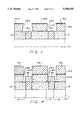
- FIGS. 1-6are cross-sectional views at various stages in the processing of wafers accordance with the present invention, in which:
- FIG. 1depicts the wafer at a stage with contact plugs and the first interlayer dielectric formed on a substrate with active devices formed thereon;
- FIG. 2depicts the wafer after tri-level resist patterning
- FIG. 3depicts the wafer after proper surface overetch
- FIG. 4depicts the wafer after metal evaporation
- FIG. 5depicts the wafer after metal lift-off
- FIG. 6depicts the wafer after dielectric spin-coat with benzocyclobutene (BCB).
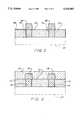
- FIG. 1depicts the incoming wafers.
- Active devicesi.e., transistors
- the substrate and active devices formed thereonare collectively denoted 10.
- Source and drain contactsmake contact to corresponding source and drain regions, while gate electrodes make contact to a thin gate oxide for forming a gate region between the source and drain region.
- the source and drain contacts and gate electrodesare separated by an oxide and are self-aligned with each other and are planarized with the oxide. Details of this aspect of the process are disclosed in a series of patents issued to Jacob D. Haskell and assigned to the same assignee as the present application (U.S. Pat. Nos.
- a first interlevel dielectric layer 12is formed and is then planarized by chemical-mechanical polishing (CMP) techniques. Contacts are defined and conventional tungsten plugs 14 are formed by blanket deposition and CMP polishing. Now the wafers are ready for the invention disclosed herein.
- CMPchemical-mechanical polishing
- Metalizationis deposited by modified conventional lift-off techniques, as now described below.
- a tri-layer resist 16is coated on the planarized surface 12a.
- the first layer 16ais a thick layer of polymethyl methacrylate (PMMA) or other polymer with proper optimization to achieve planarization.
- PMMApolymethyl methacrylate
- the thicknessis about 0.5 to 3 ⁇ m.
- the actual thicknessdepends on design choice of metal interconnect thickness and width requirements.
- a rule of thumb for the ratio of the PMMA thickness to interconnect thicknessis about 2:1 to ensure good electrical yield, that is, no defects. In other words, the metal deposited should be no more than about 50% of the PMMA thickness.
- a thin layer 16b of SiO 2 or Siis next deposited by any of plasma enhanced chemical vapor deposition (PECVD) or physical vapor deposition (PVD) or spin coating techniques.
- PECVDplasma enhanced chemical vapor deposition
- PVDphysical vapor deposition
- Other materials that may be employed for the thin layer 16binclude Si 3 N 4 , silicon oxy-nitride, sputtered silicon, amorphous silicon (e.g., by the CVD method), and amorphous carbon (e.g., by the PVD or CVD methods).
- the thicknessis about 200 to 500 ⁇ ; this layer 16b serves as the hard mask for pattern transfer.
- a thin layer 16c of conventional photoresistis coated on the hard mask layer 16b, typically to a thickness of about 5,000 to 15,000 ⁇ .
- the thickness of the thin layer 16cis a function of the wavelength used in the exposure system, e.g., G-line, I-line, or DUV (deep ultraviolet).
- the technologistmay either choose the maximum or minimum on the swing curve (the swing curve is a function of thickness). Usually, technologists choose the minimum resist thickness that corresponds to either the maximum or minimum of the swing curve.
- Conventional lithography techniquesare used to pattern the conventional photoresist layer 16c.
- the imageis transferred to the hard mask 16b by dry etch techniques, employing conventional plasma chemistry. Dry etch is again used to transfer the image from the hard mask 16b to the PMMA or polymer layer 16a.
- Appropriate plasma chemistryis used to create a slight re-entrant angle ⁇ .
- the chemistrycould employ conventional CF 4 plasma or simple O 2 plasma.
- light re-entrant angleis meant an angle of greater than 90°, preferably, greater than 100°. The resulting structure is shown in FIG. 2.
- Appropriate plasma chemistryis next used to etch the wafer surface 12a to ensure the plugs or underneath metal layers 14 are exposed at the desired location.
- the appropriate plasma chemistrycould employ either CF 4 , CHF 3 , or other fluorine chemistry with or without oxygen chemistry.
- the processing pressurewould have to be optimized to give the correct profile; however, this is not considered to constitute undue experimentation.
- the wafer surface etchingadvantageously removes the top photoresist layer 16c, depending on the choice of chemistry, although the removal may be performed in a separate step.
- the use of the hard mask 16bprotects the integrity of the PMMA during etching. The resulting structure is shown in FIG. 3.
- a high temperature bakeis performed to that ensure no out-gassing of the PMMA layer 16a interferes with the metal deposition step, described below.
- the high temperature bakeis carded out after layer 16c is removed and prior to the metal deposition. Specifically, the high temperature bake must be performed at a lower temperature than the glass transition temperature (T g ) of the PMMA layer 16a and yet higher than the metal deposition temperature for good yield.
- T gglass transition temperature
- the waferis baked at about 350° C.
- Use of another polymermay require a different baking temperature, within the constraints given above.
- the desired thickness of the metal layer 18is deposited, within the range of about 2,000 to 10,000 ⁇ .
- a thin layer of tantalum, palladium, or titanium or other refractory metal of no more than 200 to 300 ⁇is first deposited before depositing the bulk metal, employing the same techniques.
- the refractory metalhelps to reduce the metal-to-metal contact resistance.
- the preferred refractory metalis palladium.
- the finished waferis immersed into a tank of appropriate solvent that will react with the PMMA or polymer 16a.
- the PMMA or polymer 16aswells, dissolves, and lifts off the metal 18 on the surface of the hard mask 16b, leaving only those portions of the metal 18 contacting the tungsten plugs 14.
- the resulting structureis shown in FIG. 5.
- Any residual PMMA or polymer 16ais cleaned by another solvent or by appropriate plasma chemistry if deemed necessary to control defect density.
- suitable solventsinclude xylene and methyl iso-butyl ketone (MIBK). It is recommended that this process be carded out in an ultrasonic bath with agitation to enhance the lift-off of undesirable metalization.
- BCB layer 20 or a variation of BCBis spin-coated and cured on the wafer as shown in FIG. 6 which depicts the multilayer interconnect structure of the present invention.
- BCBrefers to a class of organic materials and derivatives, all manufactured by Dow Chemical (Midland, Mich.).
- An example of a BCB derivativeis divinyl siloxane bisbenzocyclobutene (DVS-BCB).
- the appropriate thickness of the BCB layer 20depends on design to give the appropriate dielectric strength, and is within the range of about 4,000 to 10,000 ⁇ . BCB is chosen because of its inert properties to metal diffusion. Copper and gold will not diffuse into BCB; therefore, BCB can serve as a good barrier. It is estimated that the same property will hold for other noble metals and low resistance metals. Further, BCB has a reported dielectric constant of about 2.4 to 2.7. This provides the desired dielectric constant, which is lower than that of silicon dioxide. The spin-coating process results in gap filling and planarization of the BCB layer 20.
- suitable low dielectric materialsmay also be employed in the practice of the present invention. These include polyimides, polyimide siloxanes, fluoropolyimides, fluoropolymers, fully cyclized heterocyclic polymers, and polysiloxanes, which have a dielectric constant in the range of about 2.2 to 3.4.
- the process of the inventioncan support any metal system without expensive hardware retooling.
- the process of the inventioncan support copper deposition with built-in barrier metal processing in the same process chamber. This lowers the cost of copper integration into existing technology.
- the process of the inventioncan support gold deposition.
- Goldis believed to be the ideal metal system for low dielectric strength ( ⁇ ) and low resistance ( ⁇ ) applications. With gold, there are no corrosion issues and no stress-induced voiding issues. Low ⁇ and low ⁇ will enhance speed-power performance for any IC, especially microprocessors.
- the power consumptionis proportional to operating frequency of the IC and the square of the capacitance C.
- Ris the resistance of the line and the RC time constant will determine the switch speed of the circuit from one state to another state, i.e., a one or a zero. Further, it is expected that superior electromigration characteristics are realized with gold, as compared to the presently-used Al alloy.
- the multilayer interconnect structure of the present inventionis expected to find use in the fabrication of semiconductor devices.
Landscapes
- Physics & Mathematics (AREA)
- Condensed Matter Physics & Semiconductors (AREA)
- General Physics & Mathematics (AREA)
- Engineering & Computer Science (AREA)
- Computer Hardware Design (AREA)
- Microelectronics & Electronic Packaging (AREA)
- Power Engineering (AREA)
- Internal Circuitry In Semiconductor Integrated Circuit Devices (AREA)
- Electrodes Of Semiconductors (AREA)
- Exposure Of Semiconductors, Excluding Electron Or Ion Beam Exposure (AREA)
Abstract
Description
Claims (10)
Priority Applications (9)
| Application Number | Priority Date | Filing Date | Title |
|---|---|---|---|
| US08/360,856US5550405A (en) | 1994-12-21 | 1994-12-21 | Processing techniques for achieving production-worthy, low dielectric, low interconnect resistance and high performance ICS |
| US08/463,448US5679608A (en) | 1994-12-21 | 1995-06-05 | Processing techniques for achieving production-worthy, low dielectric, low dielectric, low interconnect resistance and high performance IC |
| TW084107888ATW301043B (en) | 1994-12-21 | 1995-07-29 | |
| DE69514686TDE69514686T2 (en) | 1994-12-21 | 1995-11-22 | SEMICONDUCTOR ELEMENT WITH FIRST AND SECOND METALIZING LAYERS SEPARATED BY A MATERIAL OF LOW DIELECTRICITY AND METHOD FOR PRODUCING THE ELEMENT |
| JP8519801AJPH10510953A (en) | 1994-12-21 | 1995-11-22 | Novel process technology to achieve low dielectric, low wiring resistance and high performance IC suitable for manufacturing |
| KR1019970704140AKR100383392B1 (en) | 1994-12-21 | 1995-11-22 | New process technology to achieve low-value, low-wiring resistance and high-performance ICs that are valuable for productivity |
| PCT/US1995/015251WO1996019830A1 (en) | 1994-12-21 | 1995-11-22 | Novel processing techniques for achieving production-worthy, low dielectric, low interconnect resistance and high performance ic |
| EP95941455AEP0799497B1 (en) | 1994-12-21 | 1995-11-22 | Semiconductor device with first and second level interconnects separated by low dielectric constant material and method of making the same |
| US08/681,141US5965934A (en) | 1994-12-21 | 1996-07-22 | Processing techniques for achieving production-worthy, low dielectric, low interconnect resistance and high performance ICS |
Applications Claiming Priority (1)
| Application Number | Priority Date | Filing Date | Title |
|---|---|---|---|
| US08/360,856US5550405A (en) | 1994-12-21 | 1994-12-21 | Processing techniques for achieving production-worthy, low dielectric, low interconnect resistance and high performance ICS |
Related Child Applications (2)
| Application Number | Title | Priority Date | Filing Date |
|---|---|---|---|
| US08/463,448DivisionUS5679608A (en) | 1994-12-21 | 1995-06-05 | Processing techniques for achieving production-worthy, low dielectric, low dielectric, low interconnect resistance and high performance IC |
| US08/681,141ContinuationUS5965934A (en) | 1994-12-21 | 1996-07-22 | Processing techniques for achieving production-worthy, low dielectric, low interconnect resistance and high performance ICS |
Publications (1)
| Publication Number | Publication Date |
|---|---|
| US5550405Atrue US5550405A (en) | 1996-08-27 |
Family
ID=23419674
Family Applications (3)
| Application Number | Title | Priority Date | Filing Date |
|---|---|---|---|
| US08/360,856Expired - LifetimeUS5550405A (en) | 1994-12-21 | 1994-12-21 | Processing techniques for achieving production-worthy, low dielectric, low interconnect resistance and high performance ICS |
| US08/463,448Expired - LifetimeUS5679608A (en) | 1994-12-21 | 1995-06-05 | Processing techniques for achieving production-worthy, low dielectric, low dielectric, low interconnect resistance and high performance IC |
| US08/681,141Expired - LifetimeUS5965934A (en) | 1994-12-21 | 1996-07-22 | Processing techniques for achieving production-worthy, low dielectric, low interconnect resistance and high performance ICS |
Family Applications After (2)
| Application Number | Title | Priority Date | Filing Date |
|---|---|---|---|
| US08/463,448Expired - LifetimeUS5679608A (en) | 1994-12-21 | 1995-06-05 | Processing techniques for achieving production-worthy, low dielectric, low dielectric, low interconnect resistance and high performance IC |
| US08/681,141Expired - LifetimeUS5965934A (en) | 1994-12-21 | 1996-07-22 | Processing techniques for achieving production-worthy, low dielectric, low interconnect resistance and high performance ICS |
Country Status (7)
| Country | Link |
|---|---|
| US (3) | US5550405A (en) |
| EP (1) | EP0799497B1 (en) |
| JP (1) | JPH10510953A (en) |
| KR (1) | KR100383392B1 (en) |
| DE (1) | DE69514686T2 (en) |
| TW (1) | TW301043B (en) |
| WO (1) | WO1996019830A1 (en) |
Cited By (62)
| Publication number | Priority date | Publication date | Assignee | Title |
|---|---|---|---|---|
| US5650667A (en)* | 1995-10-30 | 1997-07-22 | National Semiconductor Corporation | Process of forming conductive bumps on the electrodes of semiconductor chips using lapping and the bumps thereby created |
| US5717251A (en)* | 1995-08-10 | 1998-02-10 | Nec Corporation | Semiconductor integrated circuit device having minature multi-level wiring structure low in parasitic capacitance |
| US5892285A (en)* | 1996-02-02 | 1999-04-06 | Micron Technology, Inc. | Semiconductor connection with a top surface having an enlarged recess |
| US5940732A (en)* | 1995-11-27 | 1999-08-17 | Semiconductor Energy Laboratory Co., | Method of fabricating semiconductor device |
| US5965934A (en)* | 1994-12-21 | 1999-10-12 | Advanced Micro Devices, Inc. | Processing techniques for achieving production-worthy, low dielectric, low interconnect resistance and high performance ICS |
| US5976979A (en)* | 1997-06-10 | 1999-11-02 | Industrial Technology Research Institute | Sequential oxygen plasma treatment and chemical mechanical polish (CMP) planarizing method for forming planarized low dielectric constant dielectric layer |
| US6023327A (en)* | 1998-08-10 | 2000-02-08 | Advanced Micro Devices, Inc. | System and method for detecting defects in an interlayer dielectric of a semiconductor device |
| US6080529A (en)* | 1997-12-12 | 2000-06-27 | Applied Materials, Inc. | Method of etching patterned layers useful as masking during subsequent etching or for damascene structures |
| US6146992A (en)* | 1995-11-22 | 2000-11-14 | Siemens Aktiengesellschaft | Vertically integrated semiconductor component and method of producing the same |
| US6153521A (en)* | 1998-06-04 | 2000-11-28 | Advanced Micro Devices, Inc. | Metallized interconnection structure and method of making the same |
| US6168983B1 (en) | 1996-11-05 | 2001-01-02 | Power Integrations, Inc. | Method of making a high-voltage transistor with multiple lateral conduction layers |
| US6174803B1 (en) | 1998-09-16 | 2001-01-16 | Vsli Technology | Integrated circuit device interconnection techniques |
| US6177802B1 (en) | 1998-08-10 | 2001-01-23 | Advanced Micro Devices, Inc. | System and method for detecting defects in an interlayer dielectric of a semiconductor device using the hall-effect |
| US6184128B1 (en) | 2000-01-31 | 2001-02-06 | Advanced Micro Devices, Inc. | Method using a thin resist mask for dual damascene stop layer etch |
| US6207994B1 (en) | 1996-11-05 | 2001-03-27 | Power Integrations, Inc. | High-voltage transistor with multi-layer conduction region |
| US6277203B1 (en) | 1998-09-29 | 2001-08-21 | Lam Research Corporation | Method and apparatus for cleaning low K dielectric and metal wafer surfaces |
| US6287961B1 (en) | 1999-01-04 | 2001-09-11 | Taiwan Semiconductor Manufacturing Company | Dual damascene patterned conductor layer formation method without etch stop layer |
| US6291339B1 (en)* | 1999-01-04 | 2001-09-18 | Advanced Micro Devices, Inc. | Bilayer interlayer dielectric having a substantially uniform composite interlayer dielectric constant over pattern features of varying density and method of making the same |
| US6294799B1 (en)* | 1995-11-27 | 2001-09-25 | Semiconductor Energy Laboratory Co., Ltd. | Semiconductor device and method of fabricating same |
| US6326300B1 (en) | 1998-09-21 | 2001-12-04 | Taiwan Semiconductor Manufacturing Company | Dual damascene patterned conductor layer formation method |
| US6331481B1 (en) | 1999-01-04 | 2001-12-18 | International Business Machines Corporation | Damascene etchback for low ε dielectric |
| US6331380B1 (en) | 1997-12-12 | 2001-12-18 | Applied Materials, Inc. | Method of pattern etching a low K dielectric layer |
| US6406999B1 (en)* | 1999-09-16 | 2002-06-18 | Agere Systems Guardian Corp. | Semiconductor device having reduced line width variations between tightly spaced and isolated features |
| US6413854B1 (en) | 1999-08-24 | 2002-07-02 | International Business Machines Corp. | Method to build multi level structure |
| US20020153556A1 (en)* | 1996-11-05 | 2002-10-24 | Power Integrations, Inc. | Method of making a high-voltage transistor with buried conduction regions |
| US6501130B2 (en) | 2001-01-24 | 2002-12-31 | Power Integrations, Inc. | High-voltage transistor with buried conduction layer |
| US6509220B2 (en) | 2000-11-27 | 2003-01-21 | Power Integrations, Inc. | Method of fabricating a high-voltage transistor |
| US20030047769A1 (en)* | 2001-09-07 | 2003-03-13 | Power Integrations, Inc. | High-voltage vertical transistor with a multi-layered extended drain structure |
| US20030047792A1 (en)* | 2001-09-07 | 2003-03-13 | Power Integrations, Inc. | High-voltage lateral transistor with a multi-layered extended drain structure |
| US20030057524A1 (en)* | 2001-09-07 | 2003-03-27 | Power Integrations, Inc. | Method of fabricating a high-voltage transistor with a multi-layered extended drain structure |
| US20030067077A1 (en)* | 2001-08-28 | 2003-04-10 | Silicon Integrated Systems Corp. | Organic copper diffusion barrier layer |
| US6630520B1 (en) | 1998-11-24 | 2003-10-07 | Dow Global Technologies Inc. | Composition containing a cross-linkable matrix precursor and a poragen, and a porous matrix prepared therefrom |
| US6652922B1 (en)* | 1995-06-15 | 2003-11-25 | Alliedsignal Inc. | Electron-beam processed films for microelectronics structures |
| US20040126586A1 (en)* | 2002-12-31 | 2004-07-01 | Hedrick Jeffrey C. | Composition and method to achieve reduced thermal expansion in polyarylene networks |
| US6768171B2 (en) | 2000-11-27 | 2004-07-27 | Power Integrations, Inc. | High-voltage transistor with JFET conduction channels |
| US6790792B2 (en) | 1999-01-08 | 2004-09-14 | Dow Global Technologies Inc. | Low dielectric constant polymers having good adhesion and toughness and articles made with such polymers |
| US20040209383A1 (en)* | 2003-04-17 | 2004-10-21 | Industrial Technology Research Institute | Lift-off process for protein chip |
| US20050079650A1 (en)* | 2003-10-09 | 2005-04-14 | Mancini David P. | Device including an amorphous carbon layer for improved adhesion of organic layers and method of fabrication |
| US20050133858A1 (en)* | 2001-09-07 | 2005-06-23 | Power Integrations, Inc. | High-voltage vertical transistor with a multi-gradient drain doping profile |
| US20050224792A1 (en)* | 2004-04-09 | 2005-10-13 | Taiwan Semiconductor Manufacturing Co. | Novel test structure for speeding a stress-induced voiding test and method of using same |
| US20060252906A1 (en)* | 2003-02-20 | 2006-11-09 | Godschalx James P | Method of synthesis of polyarylenes and the polyarylenes made by such method |
| CN100399563C (en)* | 2005-03-08 | 2008-07-02 | 台湾积体电路制造股份有限公司 | Semiconductor device with a plurality of semiconductor chips |
| US20080197397A1 (en)* | 2007-02-16 | 2008-08-21 | Power Integrations, Inc. | Checkerboarded high-voltage vertical transistor layout |
| US20080197418A1 (en)* | 2007-02-16 | 2008-08-21 | Power Integrations, Inc. | Gate pullback at ends of high-voltage vertical transistor structure |
| US20080197493A1 (en)* | 2007-02-16 | 2008-08-21 | Stefan Geyer | Integrated circuit including conductive bumps |
| US20080197417A1 (en)* | 2007-02-16 | 2008-08-21 | Power Integrations, Inc. | Segmented pillar layout for a high-voltage vertical transistor |
| US20080254631A1 (en)* | 2006-03-15 | 2008-10-16 | Tsutomu Shimayama | Method for fabrication of semiconductor device |
| US7468536B2 (en) | 2007-02-16 | 2008-12-23 | Power Integrations, Inc. | Gate metal routing for transistor with checkerboarded layout |
| CN100456462C (en)* | 2003-10-09 | 2009-01-28 | 飞思卡尔半导体公司 | Amorphous carbon layer to improve photoresist adhesion |
| US20090081377A1 (en)* | 2007-09-26 | 2009-03-26 | Fujifilm Corporation | Film-forming composition and production method of film |
| US20100032708A1 (en)* | 2005-11-17 | 2010-02-11 | Semiconductor Energy Laboratory Co., Ltd. | Display device and manufacturing method of the same |
| US20100065964A1 (en)* | 2008-09-15 | 2010-03-18 | Abdalla Aly Naem | Copper-topped interconnect structure that has thin and thick copper traces and method of forming the copper-topped interconnect structure |
| US7786533B2 (en) | 2001-09-07 | 2010-08-31 | Power Integrations, Inc. | High-voltage vertical transistor with edge termination structure |
| US7964934B1 (en) | 2007-05-22 | 2011-06-21 | National Semiconductor Corporation | Fuse target and method of forming the fuse target in a copper process flow |
| US8030733B1 (en) | 2007-05-22 | 2011-10-04 | National Semiconductor Corporation | Copper-compatible fuse target |
| US8653583B2 (en) | 2007-02-16 | 2014-02-18 | Power Integrations, Inc. | Sensing FET integrated with a high-voltage transistor |
| US9543396B2 (en) | 2013-12-13 | 2017-01-10 | Power Integrations, Inc. | Vertical transistor device structure with cylindrically-shaped regions |
| US9660053B2 (en) | 2013-07-12 | 2017-05-23 | Power Integrations, Inc. | High-voltage field-effect transistor having multiple implanted layers |
| US20190088500A1 (en)* | 2017-09-15 | 2019-03-21 | Globalfoundries Inc. | Interconnects formed by a metal replacement process |
| US10249764B2 (en) | 2012-02-09 | 2019-04-02 | Semiconductor Energy Laboratory Co., Ltd. | Semiconductor device, display device including semiconductor device, electronic device including semiconductor device, and method for manufacturing semiconductor device |
| US10263114B2 (en) | 2016-03-04 | 2019-04-16 | Semiconductor Energy Laboratory Co., Ltd. | Semiconductor device, method for manufacturing the same, or display device including the same |
| US10325988B2 (en) | 2013-12-13 | 2019-06-18 | Power Integrations, Inc. | Vertical transistor device structure with cylindrically-shaped field plates |
Families Citing this family (61)
| Publication number | Priority date | Publication date | Assignee | Title |
|---|---|---|---|---|
| US6429120B1 (en) | 2000-01-18 | 2002-08-06 | Micron Technology, Inc. | Methods and apparatus for making integrated-circuit wiring from copper, silver, gold, and other metals |
| US5880018A (en)* | 1996-10-07 | 1999-03-09 | Motorola Inc. | Method for manufacturing a low dielectric constant inter-level integrated circuit structure |
| JPH10242271A (en)* | 1997-02-28 | 1998-09-11 | Sony Corp | Semiconductor device and its manufacture |
| US6025116A (en)* | 1997-03-31 | 2000-02-15 | Siemens Aktiengesellschaft | Etching of contact holes |
| JP2897827B2 (en)* | 1997-04-08 | 1999-05-31 | 日本電気株式会社 | Multilayer wiring structure of semiconductor device |
| US5962067A (en) | 1997-09-09 | 1999-10-05 | Lucent Technologies Inc. | Method for coating an article with a ladder siloxane polymer and coated article |
| US6340435B1 (en) | 1998-02-11 | 2002-01-22 | Applied Materials, Inc. | Integrated low K dielectrics and etch stops |
| US6054379A (en) | 1998-02-11 | 2000-04-25 | Applied Materials, Inc. | Method of depositing a low k dielectric with organo silane |
| US6211073B1 (en) | 1998-02-27 | 2001-04-03 | Micron Technology, Inc. | Methods for making copper and other metal interconnections in integrated circuits |
| JP3469771B2 (en)* | 1998-03-24 | 2003-11-25 | 富士通株式会社 | Semiconductor device and manufacturing method thereof |
| EP1070346A1 (en) | 1998-04-02 | 2001-01-24 | Applied Materials, Inc. | Method for etching low k dielectrics |
| TW374224B (en)* | 1998-04-03 | 1999-11-11 | United Microelectronics Corp | Dual damascene process for manufacturing low k dielectrics |
| US6387819B1 (en) | 1998-04-29 | 2002-05-14 | Applied Materials, Inc. | Method for etching low K dielectric layers |
| US6232235B1 (en)* | 1998-06-03 | 2001-05-15 | Motorola, Inc. | Method of forming a semiconductor device |
| US6284656B1 (en) | 1998-08-04 | 2001-09-04 | Micron Technology, Inc. | Copper metallurgy in integrated circuits |
| US6288442B1 (en) | 1998-09-10 | 2001-09-11 | Micron Technology, Inc. | Integrated circuit with oxidation-resistant polymeric layer |
| US6284149B1 (en) | 1998-09-18 | 2001-09-04 | Applied Materials, Inc. | High-density plasma etching of carbon-based low-k materials in a integrated circuit |
| US6309926B1 (en) | 1998-12-04 | 2001-10-30 | Advanced Micro Devices | Thin resist with nitride hard mask for gate etch application |
| US6359328B1 (en)* | 1998-12-31 | 2002-03-19 | Intel Corporation | Methods for making interconnects and diffusion barriers in integrated circuits |
| US6153514A (en)* | 1999-01-04 | 2000-11-28 | Advanced Micro Devices, Inc. | Self-aligned dual damascene arrangement for metal interconnection with low k dielectric constant materials and nitride middle etch stop layer |
| US6291887B1 (en) | 1999-01-04 | 2001-09-18 | Advanced Micro Devices, Inc. | Dual damascene arrangements for metal interconnection with low k dielectric constant materials and nitride middle etch stop layer |
| US6255735B1 (en) | 1999-01-05 | 2001-07-03 | Advanced Micro Devices, Inc. | Dual damascene arrangement for metal interconnection with low k dielectric constant materials in dielectric layers |
| JP2000199968A (en)* | 1999-01-06 | 2000-07-18 | Sony Corp | Multilayered resist structure and manufacture of three- dimensional fine structure using the same |
| US6380091B1 (en) | 1999-01-27 | 2002-04-30 | Advanced Micro Devices, Inc. | Dual damascene arrangement for metal interconnection with oxide dielectric layer and low K dielectric constant layer |
| US6207577B1 (en) | 1999-01-27 | 2001-03-27 | Advanced Micro Devices, Inc. | Self-aligned dual damascene arrangement for metal interconnection with oxide dielectric layer and low k dielectric constant layer |
| US20020127845A1 (en)* | 1999-03-01 | 2002-09-12 | Paul A. Farrar | Conductive structures in integrated circuits |
| US6281135B1 (en)* | 1999-08-05 | 2001-08-28 | Axcelis Technologies, Inc. | Oxygen free plasma stripping process |
| US6492186B1 (en)* | 1999-08-05 | 2002-12-10 | Eaton Corporation | Method for detecting an endpoint for an oxygen free plasma process |
| US6137126A (en)* | 1999-08-17 | 2000-10-24 | Advanced Micro Devices, Inc. | Method to reduce gate-to-local interconnect capacitance using a low dielectric constant material for LDD spacer |
| US6309962B1 (en) | 1999-09-15 | 2001-10-30 | Taiwan Semiconductor Manufacturing Company | Film stack and etching sequence for dual damascene |
| US6297139B1 (en)* | 2000-01-10 | 2001-10-02 | United Microelectronics Corp. | Method of forming a contact hole in a semiconductor wafer |
| US7211512B1 (en) | 2000-01-18 | 2007-05-01 | Micron Technology, Inc. | Selective electroless-plated copper metallization |
| US7262130B1 (en) | 2000-01-18 | 2007-08-28 | Micron Technology, Inc. | Methods for making integrated-circuit wiring from copper, silver, gold, and other metals |
| US6376370B1 (en) | 2000-01-18 | 2002-04-23 | Micron Technology, Inc. | Process for providing seed layers for using aluminum, copper, gold and silver metallurgy process for providing seed layers for using aluminum, copper, gold and silver metallurgy |
| US6420262B1 (en) | 2000-01-18 | 2002-07-16 | Micron Technology, Inc. | Structures and methods to enhance copper metallization |
| US6469775B1 (en)* | 2000-01-31 | 2002-10-22 | Micron Technology, Inc. | Reticle for creating resist-filled vias in a dual damascene process |
| US6423629B1 (en) | 2000-05-31 | 2002-07-23 | Kie Y. Ahn | Multilevel copper interconnects with low-k dielectrics and air gaps |
| US6674167B1 (en) | 2000-05-31 | 2004-01-06 | Micron Technology, Inc. | Multilevel copper interconnect with double passivation |
| US6461963B1 (en) | 2000-08-30 | 2002-10-08 | Micron Technology, Inc. | Utilization of disappearing silicon hard mask for fabrication of semiconductor structures |
| US6851319B2 (en)* | 2000-09-27 | 2005-02-08 | Digital Wave Corporation | Device and method designed for ultrasonically inspecting cylinders for longitudinal and circumferential defects and to measure wall thickness |
| US6605519B2 (en)* | 2001-05-02 | 2003-08-12 | Unaxis Usa, Inc. | Method for thin film lift-off processes using lateral extended etching masks and device |
| US6630406B2 (en) | 2001-05-14 | 2003-10-07 | Axcelis Technologies | Plasma ashing process |
| US6951823B2 (en)* | 2001-05-14 | 2005-10-04 | Axcelis Technologies, Inc. | Plasma ashing process |
| US20030008129A1 (en) | 2001-06-27 | 2003-01-09 | International Business Machines Corporation | Dielectric material and process of insulating a semiconductor device using same |
| CN100375265C (en)* | 2002-04-02 | 2008-03-12 | 陶氏环球技术公司 | Three-layer mask structure for patterned dual damascene interconnects |
| US6939808B2 (en)* | 2002-08-02 | 2005-09-06 | Applied Materials, Inc. | Undoped and fluorinated amorphous carbon film as pattern mask for metal etch |
| US6989332B1 (en) | 2002-08-13 | 2006-01-24 | Advanced Micro Devices, Inc. | Ion implantation to modulate amorphous carbon stress |
| US6875664B1 (en) | 2002-08-29 | 2005-04-05 | Advanced Micro Devices, Inc. | Formation of amorphous carbon ARC stack having graded transition between amorphous carbon and ARC material |
| US7521304B1 (en) | 2002-08-29 | 2009-04-21 | Advanced Micro Devices, Inc. | Method for forming integrated circuit |
| US7084071B1 (en) | 2002-09-16 | 2006-08-01 | Advanced Micro Devices, Inc. | Use of multilayer amorphous carbon ARC stack to eliminate line warpage phenomenon |
| US7015124B1 (en) | 2003-04-28 | 2006-03-21 | Advanced Micro Devices, Inc. | Use of amorphous carbon for gate patterning |
| US7220665B2 (en) | 2003-08-05 | 2007-05-22 | Micron Technology, Inc. | H2 plasma treatment |
| US20050136648A1 (en)* | 2003-12-23 | 2005-06-23 | Mariah Sharma | Method and system for forming a contact in a thin-film device |
| US7229745B2 (en)* | 2004-06-14 | 2007-06-12 | Bae Systems Information And Electronic Systems Integration Inc. | Lithographic semiconductor manufacturing using a multi-layered process |
| KR100770541B1 (en)* | 2005-12-29 | 2007-10-25 | 동부일렉트로닉스 주식회사 | Semiconductor device and manufacturing method thereof |
| TW200836322A (en)* | 2007-02-16 | 2008-09-01 | Touch Micro System Tech | Method of fabricating micro connectors |
| CN100547748C (en)* | 2007-03-05 | 2009-10-07 | 探微科技股份有限公司 | Method for manufacturing micro connector |
| FR2914781B1 (en) | 2007-04-03 | 2009-11-20 | Commissariat Energie Atomique | METHOD FOR MAKING LOCALIZED DEPOSITS |
| KR101932665B1 (en)* | 2011-10-10 | 2018-12-27 | 삼성전자 주식회사 | Semiconductor package |
| US10170419B2 (en) | 2016-06-22 | 2019-01-01 | International Business Machines Corporation | Biconvex low resistance metal wire |
| JP2021141153A (en)* | 2020-03-04 | 2021-09-16 | キオクシア株式会社 | Pattern formation method and semiconductor device manufacturing method |
Citations (10)
| Publication number | Priority date | Publication date | Assignee | Title |
|---|---|---|---|---|
| US4970574A (en)* | 1988-05-31 | 1990-11-13 | Nec Corporation | Electromigrationproof structure for multilayer wiring on a semiconductor device |
| US4974055A (en)* | 1987-12-02 | 1990-11-27 | Advanced Micro Devices, Inc. | Self-aligned interconnects for semiconductor devices |
| US4977108A (en)* | 1987-12-02 | 1990-12-11 | Advanced Micro Devices, Inc. | Method of making self-aligned, planarized contacts for semiconductor devices |
| US5028555A (en)* | 1987-12-02 | 1991-07-02 | Advanced Micro Devices, Inc. | Self-aligned semiconductor devices |
| US5034801A (en)* | 1989-07-31 | 1991-07-23 | W. L. Gore & Associates, Inc. | Intergrated circuit element having a planar, solvent-free dielectric layer |
| US5055427A (en)* | 1987-12-02 | 1991-10-08 | Advanced Micro Devices, Inc. | Process of forming self-aligned interconnects for semiconductor devices |
| US5057902A (en)* | 1987-12-02 | 1991-10-15 | Advanced Micro Devices, Inc. | Self-aligned semiconductor devices |
| US5081516A (en)* | 1987-12-02 | 1992-01-14 | Advanced Micro Devices, Inc. | Self-aligned, planarized contacts for semiconductor devices |
| US5371407A (en)* | 1991-06-07 | 1994-12-06 | Norton Company | Electronic circuit with diamond substrate and conductive vias |
| US5409777A (en)* | 1990-12-10 | 1995-04-25 | The Dow Chemical Company | Laminates of polymer shaving perfluorocyclobutane rings |
Family Cites Families (18)
| Publication number | Priority date | Publication date | Assignee | Title |
|---|---|---|---|---|
| US4219925A (en)* | 1978-09-01 | 1980-09-02 | Teletype Corporation | Method of manufacturing a device in a silicon wafer |
| US4410622A (en)* | 1978-12-29 | 1983-10-18 | International Business Machines Corporation | Forming interconnections for multilevel interconnection metallurgy systems |
| US4367119A (en)* | 1980-08-18 | 1983-01-04 | International Business Machines Corporation | Planar multi-level metal process with built-in etch stop |
| JPS5982746A (en)* | 1982-11-04 | 1984-05-12 | Toshiba Corp | Electrode wiring method of semiconductor device |
| US4507333A (en)* | 1982-11-22 | 1985-03-26 | International Business Machines Corporation | Biphenylene end-capped quinoxaline polymers and their use as insulating coatings for semiconductor devices |
| US4493855A (en)* | 1982-12-23 | 1985-01-15 | International Business Machines Corporation | Use of plasma polymerized organosilicon films in fabrication of lift-off masks |
| JPS60142545A (en)* | 1983-12-27 | 1985-07-27 | インタ−ナショナル ビジネス マシ−ンズ コ−ポレ−ション | Multilayer composite structure |
| US4508812A (en)* | 1984-05-03 | 1985-04-02 | Hughes Aircraft Company | Method of applying poly(methacrylic anhydride resist to a semiconductor |
| US4523372A (en)* | 1984-05-07 | 1985-06-18 | Motorola, Inc. | Process for fabricating semiconductor device |
| JP2532589B2 (en)* | 1988-06-29 | 1996-09-11 | 松下電器産業株式会社 | Fine pattern formation method |
| US5057399A (en)* | 1989-03-31 | 1991-10-15 | Tony Flaim | Method for making polyimide microlithographic compositions soluble in alkaline media |
| US5282922A (en)* | 1989-11-16 | 1994-02-01 | Polycon Corporation | Hybrid circuit structures and methods of fabrication |
| US5116463A (en)* | 1991-06-19 | 1992-05-26 | Microelectroncs And Computer Technology Corporation | Detecting completion of electroless via fill |
| US5300813A (en)* | 1992-02-26 | 1994-04-05 | International Business Machines Corporation | Refractory metal capped low resistivity metal conductor lines and vias |
| US5486493A (en)* | 1994-02-25 | 1996-01-23 | Jeng; Shin-Puu | Planarized multi-level interconnect scheme with embedded low-dielectric constant insulators |
| US5461003A (en)* | 1994-05-27 | 1995-10-24 | Texas Instruments Incorporated | Multilevel interconnect structure with air gaps formed between metal leads |
| EP0690494B1 (en)* | 1994-06-27 | 2004-03-17 | Infineon Technologies AG | Connection and build-up-process for multi-chip-modules |
| US5550405A (en)* | 1994-12-21 | 1996-08-27 | Advanced Micro Devices, Incorporated | Processing techniques for achieving production-worthy, low dielectric, low interconnect resistance and high performance ICS |
- 1994
- 1994-12-21USUS08/360,856patent/US5550405A/ennot_activeExpired - Lifetime
- 1995
- 1995-06-05USUS08/463,448patent/US5679608A/ennot_activeExpired - Lifetime
- 1995-07-29TWTW084107888Apatent/TW301043B/zhnot_activeIP Right Cessation
- 1995-11-22KRKR1019970704140Apatent/KR100383392B1/ennot_activeExpired - Lifetime
- 1995-11-22EPEP95941455Apatent/EP0799497B1/ennot_activeExpired - Lifetime
- 1995-11-22DEDE69514686Tpatent/DE69514686T2/ennot_activeExpired - Fee Related
- 1995-11-22JPJP8519801Apatent/JPH10510953A/ennot_activeCeased
- 1995-11-22WOPCT/US1995/015251patent/WO1996019830A1/enactiveIP Right Grant
- 1996
- 1996-07-22USUS08/681,141patent/US5965934A/ennot_activeExpired - Lifetime
Patent Citations (10)
| Publication number | Priority date | Publication date | Assignee | Title |
|---|---|---|---|---|
| US4974055A (en)* | 1987-12-02 | 1990-11-27 | Advanced Micro Devices, Inc. | Self-aligned interconnects for semiconductor devices |
| US4977108A (en)* | 1987-12-02 | 1990-12-11 | Advanced Micro Devices, Inc. | Method of making self-aligned, planarized contacts for semiconductor devices |
| US5028555A (en)* | 1987-12-02 | 1991-07-02 | Advanced Micro Devices, Inc. | Self-aligned semiconductor devices |
| US5055427A (en)* | 1987-12-02 | 1991-10-08 | Advanced Micro Devices, Inc. | Process of forming self-aligned interconnects for semiconductor devices |
| US5057902A (en)* | 1987-12-02 | 1991-10-15 | Advanced Micro Devices, Inc. | Self-aligned semiconductor devices |
| US5081516A (en)* | 1987-12-02 | 1992-01-14 | Advanced Micro Devices, Inc. | Self-aligned, planarized contacts for semiconductor devices |
| US4970574A (en)* | 1988-05-31 | 1990-11-13 | Nec Corporation | Electromigrationproof structure for multilayer wiring on a semiconductor device |
| US5034801A (en)* | 1989-07-31 | 1991-07-23 | W. L. Gore & Associates, Inc. | Intergrated circuit element having a planar, solvent-free dielectric layer |
| US5409777A (en)* | 1990-12-10 | 1995-04-25 | The Dow Chemical Company | Laminates of polymer shaving perfluorocyclobutane rings |
| US5371407A (en)* | 1991-06-07 | 1994-12-06 | Norton Company | Electronic circuit with diamond substrate and conductive vias |
Non-Patent Citations (2)
| Title |
|---|
| No Author, "Multilevel Interconnection Structure," IBM Technical Disclosure Bulletin, vol. 34, No. 9, Feb. 1992, p. 220. |
| No Author, Multilevel Interconnection Structure, IBM Technical Disclosure Bulletin, vol. 34, No. 9, Feb. 1992, p. 220.* |
Cited By (149)
| Publication number | Priority date | Publication date | Assignee | Title |
|---|---|---|---|---|
| US5965934A (en)* | 1994-12-21 | 1999-10-12 | Advanced Micro Devices, Inc. | Processing techniques for achieving production-worthy, low dielectric, low interconnect resistance and high performance ICS |
| US20040076764A1 (en)* | 1995-06-15 | 2004-04-22 | Lynn Forester | Electron-beam processed films for microelectronics structures |
| US6652922B1 (en)* | 1995-06-15 | 2003-11-25 | Alliedsignal Inc. | Electron-beam processed films for microelectronics structures |
| US5717251A (en)* | 1995-08-10 | 1998-02-10 | Nec Corporation | Semiconductor integrated circuit device having minature multi-level wiring structure low in parasitic capacitance |
| US5650667A (en)* | 1995-10-30 | 1997-07-22 | National Semiconductor Corporation | Process of forming conductive bumps on the electrodes of semiconductor chips using lapping and the bumps thereby created |
| US20050287722A1 (en)* | 1995-11-19 | 2005-12-29 | Semiconductor Energy Laboratory Co., Ltd., A Japan Corporation | Method of fabricating semiconductor device |
| US6146992A (en)* | 1995-11-22 | 2000-11-14 | Siemens Aktiengesellschaft | Vertically integrated semiconductor component and method of producing the same |
| US5940732A (en)* | 1995-11-27 | 1999-08-17 | Semiconductor Energy Laboratory Co., | Method of fabricating semiconductor device |
| US6740599B2 (en)* | 1995-11-27 | 2004-05-25 | Shunpei Yamazaki | Method of fabricating contact holes in a semiconductor device |
| US6294799B1 (en)* | 1995-11-27 | 2001-09-25 | Semiconductor Energy Laboratory Co., Ltd. | Semiconductor device and method of fabricating same |
| US6972263B2 (en) | 1995-11-27 | 2005-12-06 | Semiconductor Energy Laboratory Co., Ltd. | Fabricating a tapered hole incorporating a resinous silicon containing film |
| US8283788B2 (en) | 1995-11-27 | 2012-10-09 | Semiconductor Energy Laboratory Co., Ltd. | Method of fabricating semiconductor device |
| US20060060861A1 (en)* | 1995-11-27 | 2006-03-23 | Semiconductor Energy Laboratory Co., Ltd. | Semiconductor device and method of fabricating same |
| US7727898B2 (en) | 1995-11-27 | 2010-06-01 | Semiconductor Energy Laboratory Co., Ltd | Semiconductor device and method of fabricating same |
| US20100200999A1 (en)* | 1995-11-27 | 2010-08-12 | Semiconductor Energy Laboratory Co., Ltd. | Semiconductor device and method of fabricating same |
| US20040192025A1 (en)* | 1995-11-27 | 2004-09-30 | Semiconductor Energy Laboratory Co., Ltd., A Japan Corporation | Semiconductor device and method of fabricating same |
| US7786553B1 (en) | 1995-11-27 | 2010-08-31 | Semiconductor Energy Laboratory Co., Ltd. | Method of fabricating semiconductor device |
| US7800235B2 (en) | 1995-11-27 | 2010-09-21 | Semiconductor Energy Laboratory Co., Ltd. | Method of fabricating semiconductor device |
| US20110001192A1 (en)* | 1995-11-27 | 2011-01-06 | Semiconductor Energy Laboratory Co., Ltd. | Method of Fabricating Semiconductor Device |
| US5892285A (en)* | 1996-02-02 | 1999-04-06 | Micron Technology, Inc. | Semiconductor connection with a top surface having an enlarged recess |
| US6277731B1 (en) | 1996-02-02 | 2001-08-21 | Micron Technology, Inc. | Method for forming a semiconductor connection with a top surface having an enlarged recess |
| US6426287B2 (en) | 1996-02-02 | 2002-07-30 | Micron Technology, Inc. | Method for forming a semiconductor connection with a top surface having an enlarged recess |
| US6448656B1 (en) | 1996-02-02 | 2002-09-10 | Micron Technology, Inc. | System including a memory device having a semiconductor connection with a top surface having an enlarged recess |
| US6066559A (en)* | 1996-02-02 | 2000-05-23 | Micron Technology, Inc. | Method for forming a semiconductor connection with a top surface having an enlarged recess |
| US6043151A (en)* | 1996-02-02 | 2000-03-28 | Micron Technology, Inc. | Method for forming a semiconductor connection with a top surface having an enlarged recess |
| US5994220A (en)* | 1996-02-02 | 1999-11-30 | Micron Technology, Inc. | Method for forming a semiconductor connection with a top surface having an enlarged recess |
| US6639277B2 (en) | 1996-11-05 | 2003-10-28 | Power Integrations, Inc. | High-voltage transistor with multi-layer conduction region |
| US20040207012A1 (en)* | 1996-11-05 | 2004-10-21 | Power Integrations, Inc. | High-voltage transistor with multi-layer conduction region |
| US6828631B2 (en) | 1996-11-05 | 2004-12-07 | Power Integrations, Inc | High-voltage transistor with multi-layer conduction region |
| US20030151093A1 (en)* | 1996-11-05 | 2003-08-14 | Power Integrations, Inc. | High-voltage transistor with multi-layer conduction region |
| US6724041B2 (en) | 1996-11-05 | 2004-04-20 | Power Integrations, Inc. | Method of making a high-voltage transistor with buried conduction regions |
| US20040217419A1 (en)* | 1996-11-05 | 2004-11-04 | Power Integrations, Inc. | High-voltage transistor with multi-layer conduction region |
| US20030151101A1 (en)* | 1996-11-05 | 2003-08-14 | Power Integrations, Inc. | High-voltage transistor with multi-layer conduction region |
| US20020153556A1 (en)* | 1996-11-05 | 2002-10-24 | Power Integrations, Inc. | Method of making a high-voltage transistor with buried conduction regions |
| US6570219B1 (en) | 1996-11-05 | 2003-05-27 | Power Integrations, Inc. | High-voltage transistor with multi-layer conduction region |
| US6633065B2 (en) | 1996-11-05 | 2003-10-14 | Power Integrations, Inc. | High-voltage transistor with multi-layer conduction region |
| US6768172B2 (en) | 1996-11-05 | 2004-07-27 | Power Integrations, Inc. | High-voltage transistor with multi-layer conduction region |
| US6787437B2 (en) | 1996-11-05 | 2004-09-07 | Power Integrations, Inc. | Method of making a high-voltage transistor with buried conduction regions |
| US6207994B1 (en) | 1996-11-05 | 2001-03-27 | Power Integrations, Inc. | High-voltage transistor with multi-layer conduction region |
| US6777749B2 (en) | 1996-11-05 | 2004-08-17 | Power Integrations, Inc. | High-voltage transistor with multi-layer conduction region |
| US6800903B2 (en) | 1996-11-05 | 2004-10-05 | Power Integrations, Inc. | High-voltage transistor with multi-layer conduction region |
| US6168983B1 (en) | 1996-11-05 | 2001-01-02 | Power Integrations, Inc. | Method of making a high-voltage transistor with multiple lateral conduction layers |
| US5976979A (en)* | 1997-06-10 | 1999-11-02 | Industrial Technology Research Institute | Sequential oxygen plasma treatment and chemical mechanical polish (CMP) planarizing method for forming planarized low dielectric constant dielectric layer |
| US6458516B1 (en) | 1997-12-12 | 2002-10-01 | Applied Materials Inc. | Method of etching dielectric layers using a removable hardmask |
| US6143476A (en)* | 1997-12-12 | 2000-11-07 | Applied Materials Inc | Method for high temperature etching of patterned layers using an organic mask stack |
| US6080529A (en)* | 1997-12-12 | 2000-06-27 | Applied Materials, Inc. | Method of etching patterned layers useful as masking during subsequent etching or for damascene structures |
| US6331380B1 (en) | 1997-12-12 | 2001-12-18 | Applied Materials, Inc. | Method of pattern etching a low K dielectric layer |
| US6153521A (en)* | 1998-06-04 | 2000-11-28 | Advanced Micro Devices, Inc. | Metallized interconnection structure and method of making the same |
| US6492722B1 (en) | 1998-06-04 | 2002-12-10 | Advanced Micro Devices, Inc. | Metallized interconnection structure |
| US6177802B1 (en) | 1998-08-10 | 2001-01-23 | Advanced Micro Devices, Inc. | System and method for detecting defects in an interlayer dielectric of a semiconductor device using the hall-effect |
| US6023327A (en)* | 1998-08-10 | 2000-02-08 | Advanced Micro Devices, Inc. | System and method for detecting defects in an interlayer dielectric of a semiconductor device |
| US6174803B1 (en) | 1998-09-16 | 2001-01-16 | Vsli Technology | Integrated circuit device interconnection techniques |
| US6326300B1 (en) | 1998-09-21 | 2001-12-04 | Taiwan Semiconductor Manufacturing Company | Dual damascene patterned conductor layer formation method |
| US6319330B1 (en) | 1998-09-29 | 2001-11-20 | Lam Research Corporation | Method and apparatus for cleaning low K dielectric and metal wafer surfaces |
| US6277203B1 (en) | 1998-09-29 | 2001-08-21 | Lam Research Corporation | Method and apparatus for cleaning low K dielectric and metal wafer surfaces |
| US7109249B2 (en) | 1998-11-24 | 2006-09-19 | Dow Global Technologies Inc. | Composition containing a cross-linkable matrix precursor and a poragen, and porous matrix prepared therefrom |
| US6887910B2 (en) | 1998-11-24 | 2005-05-03 | Dow Global Technologies Inc. | Composition containing a cross-linkable matrix precursor and a poragen, and a porous matrix prepared therefrom |
| US6653358B2 (en) | 1998-11-24 | 2003-11-25 | Dow Global Technologies Inc. | Composition containing a cross-linkable matrix precursor and a poragen, and a porous matrix prepared therefrom |
| US20050014855A1 (en)* | 1998-11-24 | 2005-01-20 | Bruza Kenneth J. | Composition containing a cross-linkable matrix precursor and a poragen, and a porous matrix prepared therefrom |
| US6630520B1 (en) | 1998-11-24 | 2003-10-07 | Dow Global Technologies Inc. | Composition containing a cross-linkable matrix precursor and a poragen, and a porous matrix prepared therefrom |
| US6331481B1 (en) | 1999-01-04 | 2001-12-18 | International Business Machines Corporation | Damascene etchback for low ε dielectric |
| US6291339B1 (en)* | 1999-01-04 | 2001-09-18 | Advanced Micro Devices, Inc. | Bilayer interlayer dielectric having a substantially uniform composite interlayer dielectric constant over pattern features of varying density and method of making the same |
| US6287961B1 (en) | 1999-01-04 | 2001-09-11 | Taiwan Semiconductor Manufacturing Company | Dual damascene patterned conductor layer formation method without etch stop layer |
| US6790792B2 (en) | 1999-01-08 | 2004-09-14 | Dow Global Technologies Inc. | Low dielectric constant polymers having good adhesion and toughness and articles made with such polymers |
| US6413854B1 (en) | 1999-08-24 | 2002-07-02 | International Business Machines Corp. | Method to build multi level structure |
| US6406999B1 (en)* | 1999-09-16 | 2002-06-18 | Agere Systems Guardian Corp. | Semiconductor device having reduced line width variations between tightly spaced and isolated features |
| US6184128B1 (en) | 2000-01-31 | 2001-02-06 | Advanced Micro Devices, Inc. | Method using a thin resist mask for dual damascene stop layer etch |
| US6768171B2 (en) | 2000-11-27 | 2004-07-27 | Power Integrations, Inc. | High-voltage transistor with JFET conduction channels |
| US6509220B2 (en) | 2000-11-27 | 2003-01-21 | Power Integrations, Inc. | Method of fabricating a high-voltage transistor |
| US6504209B2 (en) | 2001-01-24 | 2003-01-07 | Power Integrations, Inc. | High-voltage transistor with buried conduction layer |
| US6818490B2 (en) | 2001-01-24 | 2004-11-16 | Power Integrations, Inc. | Method of fabricating complementary high-voltage field-effect transistors |
| US6501130B2 (en) | 2001-01-24 | 2002-12-31 | Power Integrations, Inc. | High-voltage transistor with buried conduction layer |
| US20040036115A1 (en)* | 2001-01-24 | 2004-02-26 | Power Integrations, Inc. | High-voltage transistor with buried conduction layer |
| US20030067077A1 (en)* | 2001-08-28 | 2003-04-10 | Silicon Integrated Systems Corp. | Organic copper diffusion barrier layer |
| US6555873B2 (en) | 2001-09-07 | 2003-04-29 | Power Integrations, Inc. | High-voltage lateral transistor with a multi-layered extended drain structure |
| US20030151110A1 (en)* | 2001-09-07 | 2003-08-14 | Power Integrations, Inc. | High-voltage lateral transistor with a multi-layered extended drain structure |
| US6815293B2 (en) | 2001-09-07 | 2004-11-09 | Power Intergrations, Inc. | High-voltage lateral transistor with a multi-layered extended drain structure |
| US7745291B2 (en) | 2001-09-07 | 2010-06-29 | Power Integrations, Inc. | Method of fabricating a high-voltage transistor with an extended drain structure |
| US20030060001A1 (en)* | 2001-09-07 | 2003-03-27 | Power Integrations, Inc. | Method of fabricating a high-voltage transistor with a multi-layered extended drain structure |
| US20040232486A1 (en)* | 2001-09-07 | 2004-11-25 | Power Integrations, Inc. | High-voltage lateral transistor with a multi-layered extended drain structure |
| US20030047793A1 (en)* | 2001-09-07 | 2003-03-13 | Power Integrations, Inc. | High-voltage vertical transistor with a multi-layered extended drain structure |
| US6667213B2 (en) | 2001-09-07 | 2003-12-23 | Power Integrations, Inc. | Method of fabricating a high-voltage transistor with a multi-layered extended drain structure |
| US20050023571A1 (en)* | 2001-09-07 | 2005-02-03 | Power Integrations, Inc. | High-voltage vertical transistor with a multi-layered extended drain structure |
| US7786533B2 (en) | 2001-09-07 | 2010-08-31 | Power Integrations, Inc. | High-voltage vertical transistor with edge termination structure |
| US6635544B2 (en) | 2001-09-07 | 2003-10-21 | Power Intergrations, Inc. | Method of fabricating a high-voltage transistor with a multi-layered extended drain structure |
| US20050104121A1 (en)* | 2001-09-07 | 2005-05-19 | Power Integrations, Inc. | Method of fabricating a high-voltage transistor with an extended drain structure |
| US20050133858A1 (en)* | 2001-09-07 | 2005-06-23 | Power Integrations, Inc. | High-voltage vertical transistor with a multi-gradient drain doping profile |
| US20030047792A1 (en)* | 2001-09-07 | 2003-03-13 | Power Integrations, Inc. | High-voltage lateral transistor with a multi-layered extended drain structure |
| US20090233407A1 (en)* | 2001-09-07 | 2009-09-17 | Power Integrations, Inc. | Method of fabricating a high-voltage transistor with an extended drain structure |
| US7221011B2 (en) | 2001-09-07 | 2007-05-22 | Power Integrations, Inc. | High-voltage vertical transistor with a multi-gradient drain doping profile |
| US6573558B2 (en) | 2001-09-07 | 2003-06-03 | Power Integrations, Inc. | High-voltage vertical transistor with a multi-layered extended drain structure |
| US6987299B2 (en) | 2001-09-07 | 2006-01-17 | Power Integrations, Inc. | High-voltage lateral transistor with a multi-layered extended drain structure |
| US20030047769A1 (en)* | 2001-09-07 | 2003-03-13 | Power Integrations, Inc. | High-voltage vertical transistor with a multi-layered extended drain structure |
| US20030057524A1 (en)* | 2001-09-07 | 2003-03-27 | Power Integrations, Inc. | Method of fabricating a high-voltage transistor with a multi-layered extended drain structure |
| US6781198B2 (en) | 2001-09-07 | 2004-08-24 | Power Integrations, Inc. | High-voltage vertical transistor with a multi-layered extended drain structure |
| US7998817B2 (en) | 2001-09-07 | 2011-08-16 | Power Integrations, Inc. | Method of fabricating a high-voltage transistor with an extended drain structure |
| US6750105B2 (en) | 2001-09-07 | 2004-06-15 | Power Integrations, Inc. | Method of fabricating a high-voltage transistor with a multi-layered extended drain structure |
| US7459366B2 (en) | 2001-09-07 | 2008-12-02 | Power Integrations, Inc. | High-voltage vertical transistor with a multi-gradient drain doping profile |
| US7829944B2 (en) | 2001-09-07 | 2010-11-09 | Power Integrations, Inc. | High-voltage vertical transistor with a multi-layered extended drain structure |
| US7253042B2 (en) | 2001-09-07 | 2007-08-07 | Power Integrations, Inc. | Method of fabricating a high-voltage transistor with an extended drain structure |
| US20070293002A1 (en)* | 2001-09-07 | 2007-12-20 | Power Intergrations, Inc. | Method of fabricating a high-voltage transistor with an extended drain structure |
| US20080102581A1 (en)* | 2001-09-07 | 2008-05-01 | Power Integrations, Inc. | High-voltage vertical transistor with a multi-gradient drain doping profile |
| US6798020B2 (en)* | 2001-09-07 | 2004-09-28 | Power Integrations, Inc. | High-voltage lateral transistor with a multi-layered extended drain structure |
| US8940605B2 (en) | 2001-09-07 | 2015-01-27 | Power Integrations, Inc. | Method of fabricating a high-voltage transistor with an extended drain structure |
| US8552496B2 (en) | 2001-09-07 | 2013-10-08 | Power Integrations, Inc. | High-voltage vertical transistor with edge termination structure |
| US6787847B2 (en) | 2001-09-07 | 2004-09-07 | Power Integrations, Inc. | High-voltage vertical transistor with a multi-layered extended drain structure |
| US6818285B2 (en) | 2002-12-31 | 2004-11-16 | International Business Machines Corporation | Composition and method to achieve reduced thermal expansion in polyarylene networks |
| US20040126586A1 (en)* | 2002-12-31 | 2004-07-01 | Hedrick Jeffrey C. | Composition and method to achieve reduced thermal expansion in polyarylene networks |
| US20060252906A1 (en)* | 2003-02-20 | 2006-11-09 | Godschalx James P | Method of synthesis of polyarylenes and the polyarylenes made by such method |
| US20040209383A1 (en)* | 2003-04-17 | 2004-10-21 | Industrial Technology Research Institute | Lift-off process for protein chip |
| WO2005038865A3 (en)* | 2003-10-09 | 2005-06-30 | Freescale Semiconductor Inc | Amorphous carbon layer to improve photoresist adhesion |
| CN100456462C (en)* | 2003-10-09 | 2009-01-28 | 飞思卡尔半导体公司 | Amorphous carbon layer to improve photoresist adhesion |
| US20050079650A1 (en)* | 2003-10-09 | 2005-04-14 | Mancini David P. | Device including an amorphous carbon layer for improved adhesion of organic layers and method of fabrication |
| US6992371B2 (en)* | 2003-10-09 | 2006-01-31 | Freescale Semiconductor, Inc. | Device including an amorphous carbon layer for improved adhesion of organic layers and method of fabrication |
| US20070109008A1 (en)* | 2004-04-09 | 2007-05-17 | Taiwan Semiconductor Manufacturing Co., Ltd. | Novel test structure for speeding a stress-induced voiding test and method of using the same |
| US20050224792A1 (en)* | 2004-04-09 | 2005-10-13 | Taiwan Semiconductor Manufacturing Co. | Novel test structure for speeding a stress-induced voiding test and method of using same |
| US7157925B2 (en) | 2004-04-09 | 2007-01-02 | Taiwan Semiconductor Manufacturing Co., Ltd. | Test structure for speeding a stress-induced voiding test and method of using same |
| CN100399563C (en)* | 2005-03-08 | 2008-07-02 | 台湾积体电路制造股份有限公司 | Semiconductor device with a plurality of semiconductor chips |
| US20100032708A1 (en)* | 2005-11-17 | 2010-02-11 | Semiconductor Energy Laboratory Co., Ltd. | Display device and manufacturing method of the same |
| US8344379B2 (en) | 2005-11-17 | 2013-01-01 | Semiconductor Energy Laboratory Co., Ltd. | Display device and manufacturing method of the same |
| US20080254631A1 (en)* | 2006-03-15 | 2008-10-16 | Tsutomu Shimayama | Method for fabrication of semiconductor device |
| US8759222B2 (en)* | 2006-03-15 | 2014-06-24 | Sony Corporation | Method for fabrication of semiconductor device |
| US8222691B2 (en) | 2007-02-16 | 2012-07-17 | Power Integrations, Inc. | Gate pullback at ends of high-voltage vertical transistor structure |
| US8022456B2 (en) | 2007-02-16 | 2011-09-20 | Power Integrations, Inc. | Checkerboarded high-voltage vertical transistor layout |
| US7595523B2 (en) | 2007-02-16 | 2009-09-29 | Power Integrations, Inc. | Gate pullback at ends of high-voltage vertical transistor structure |
| US7557406B2 (en) | 2007-02-16 | 2009-07-07 | Power Integrations, Inc. | Segmented pillar layout for a high-voltage vertical transistor |
| US7859037B2 (en) | 2007-02-16 | 2010-12-28 | Power Integrations, Inc. | Checkerboarded high-voltage vertical transistor layout |
| US8410551B2 (en) | 2007-02-16 | 2013-04-02 | Power Integrations, Inc. | Checkerboarded high-voltage vertical transistor layout |
| US20080197397A1 (en)* | 2007-02-16 | 2008-08-21 | Power Integrations, Inc. | Checkerboarded high-voltage vertical transistor layout |
| US20110089476A1 (en)* | 2007-02-16 | 2011-04-21 | Power Integrations, Inc. | Checkerboarded high-voltage vertical transistor layout |
| US7468536B2 (en) | 2007-02-16 | 2008-12-23 | Power Integrations, Inc. | Gate metal routing for transistor with checkerboarded layout |
| US20080197493A1 (en)* | 2007-02-16 | 2008-08-21 | Stefan Geyer | Integrated circuit including conductive bumps |
| US8653583B2 (en) | 2007-02-16 | 2014-02-18 | Power Integrations, Inc. | Sensing FET integrated with a high-voltage transistor |
| US20080197418A1 (en)* | 2007-02-16 | 2008-08-21 | Power Integrations, Inc. | Gate pullback at ends of high-voltage vertical transistor structure |
| US20080197417A1 (en)* | 2007-02-16 | 2008-08-21 | Power Integrations, Inc. | Segmented pillar layout for a high-voltage vertical transistor |
| US8030733B1 (en) | 2007-05-22 | 2011-10-04 | National Semiconductor Corporation | Copper-compatible fuse target |
| US7964934B1 (en) | 2007-05-22 | 2011-06-21 | National Semiconductor Corporation | Fuse target and method of forming the fuse target in a copper process flow |
| US20090081377A1 (en)* | 2007-09-26 | 2009-03-26 | Fujifilm Corporation | Film-forming composition and production method of film |
| US8324097B2 (en)* | 2008-09-15 | 2012-12-04 | National Semiconductor Corporation | Method of forming a copper topped interconnect structure that has thin and thick copper traces |
| US20100190332A1 (en)* | 2008-09-15 | 2010-07-29 | Abdalla Aly Naem | Method of Forming a Copper Topped Interconnect Structure that has Thin and Thick Copper Traces |
| US20100065964A1 (en)* | 2008-09-15 | 2010-03-18 | Abdalla Aly Naem | Copper-topped interconnect structure that has thin and thick copper traces and method of forming the copper-topped interconnect structure |
| US7709956B2 (en) | 2008-09-15 | 2010-05-04 | National Semiconductor Corporation | Copper-topped interconnect structure that has thin and thick copper traces and method of forming the copper-topped interconnect structure |
| US10249764B2 (en) | 2012-02-09 | 2019-04-02 | Semiconductor Energy Laboratory Co., Ltd. | Semiconductor device, display device including semiconductor device, electronic device including semiconductor device, and method for manufacturing semiconductor device |
| US9660053B2 (en) | 2013-07-12 | 2017-05-23 | Power Integrations, Inc. | High-voltage field-effect transistor having multiple implanted layers |
| US9543396B2 (en) | 2013-12-13 | 2017-01-10 | Power Integrations, Inc. | Vertical transistor device structure with cylindrically-shaped regions |
| US10325988B2 (en) | 2013-12-13 | 2019-06-18 | Power Integrations, Inc. | Vertical transistor device structure with cylindrically-shaped field plates |
| US10263114B2 (en) | 2016-03-04 | 2019-04-16 | Semiconductor Energy Laboratory Co., Ltd. | Semiconductor device, method for manufacturing the same, or display device including the same |
| US20190088500A1 (en)* | 2017-09-15 | 2019-03-21 | Globalfoundries Inc. | Interconnects formed by a metal replacement process |
| US10283372B2 (en)* | 2017-09-15 | 2019-05-07 | Globalfoundries Inc. | Interconnects formed by a metal replacement process |
Also Published As
| Publication number | Publication date |
|---|---|
| TW301043B (en) | 1997-03-21 |
| DE69514686D1 (en) | 2000-02-24 |
| JPH10510953A (en) | 1998-10-20 |
| US5965934A (en) | 1999-10-12 |
| EP0799497A1 (en) | 1997-10-08 |
| DE69514686T2 (en) | 2000-08-31 |
| US5679608A (en) | 1997-10-21 |
| KR100383392B1 (en) | 2003-07-18 |
| EP0799497B1 (en) | 2000-01-19 |
| KR980700690A (en) | 1998-03-30 |
| WO1996019830A1 (en) | 1996-06-27 |
Similar Documents
| Publication | Publication Date | Title |
|---|---|---|
| US5550405A (en) | Processing techniques for achieving production-worthy, low dielectric, low interconnect resistance and high performance ICS | |
| US6806192B2 (en) | Method of barrier-less integration with copper alloy | |
| US6071809A (en) | Methods for forming high-performing dual-damascene interconnect structures | |
| US6509258B2 (en) | Etch stop in damascene interconnect structure and method of making | |
| JP4230334B2 (en) | Semiconductor device and manufacturing method thereof | |
| US6943111B2 (en) | Barrier free copper interconnect by multi-layer copper seed | |
| US20020155693A1 (en) | Method to form self-aligned anti-via interconnects | |
| US6573572B2 (en) | Damascene structure and method of making | |
| JP5334616B2 (en) | Method for making an interconnect | |
| JPH1174356A (en) | Improved double damascene structure | |
| JP2000188293A (en) | Method for optimizing chemical-mechanical polishing of copper in copper interconnecting process for integrated circuit | |
| JP2009135518A (en) | Mutual connection manufacturing method | |
| KR100860133B1 (en) | Local Increase in Sidewall Density by Ion Implantation | |
| KR100473513B1 (en) | Method for dual-damascene patterning of low-k interconnects using spin-on distributed hardmask | |
| US20030067077A1 (en) | Organic copper diffusion barrier layer | |
| US6821896B1 (en) | Method to eliminate via poison effect | |
| US20030096496A1 (en) | Method of forming dual damascene structure | |
| US20040157392A1 (en) | Capacitor in an interconnect system and method of manufacturing thereof | |
| US6800548B2 (en) | Method to avoid via poisoning in dual damascene process | |
| CN1684244B (en) | Method for manufacturing semiconductor device with air gap damascene structure | |
| US6927160B1 (en) | Fabrication of copper-containing region such as electrical interconnect | |
| JP2004508713A (en) | Subtractive metallized structure and method of manufacturing the same | |
| US7381638B1 (en) | Fabrication technique using sputter etch and vacuum transfer | |
| TW511241B (en) | Method of forming a dual damascene via by using a metal hard mask layer | |
| Shacham‐Diamand et al. | Optical and electron beam lithography for electroless copper multilevel metallization |
Legal Events
| Date | Code | Title | Description |
|---|---|---|---|
| AS | Assignment | Owner name:ADVANCED MICRO DEVICES, INC., CALIFORNIA Free format text:ASSIGNMENT OF ASSIGNORS INTEREST;ASSIGNORS:CHEUNG, ROBIN W.;CHANG, MARK S.;REEL/FRAME:007307/0655 Effective date:19941219 | |
| STCF | Information on status: patent grant | Free format text:PATENTED CASE | |
| FPAY | Fee payment | Year of fee payment:4 | |
| FPAY | Fee payment | Year of fee payment:8 | |
| AS | Assignment | Owner name:SPANSION INC., CALIFORNIA Free format text:ASSIGNMENT OF ASSIGNORS INTEREST;ASSIGNOR:ADVANCED MICRO DEVICES, INC.;REEL/FRAME:019028/0599 Effective date:20070131 | |
| AS | Assignment | Owner name:SPANSION LLC, CALIFORNIA Free format text:ASSIGNMENT OF ASSIGNORS INTEREST;ASSIGNOR:SPANSION INC.;REEL/FRAME:019063/0771 Effective date:20070131 | |
| FPAY | Fee payment | Year of fee payment:12 | |
| AS | Assignment | Owner name:BARCLAYS BANK PLC,NEW YORK Free format text:SECURITY AGREEMENT;ASSIGNORS:SPANSION LLC;SPANSION INC.;SPANSION TECHNOLOGY INC.;AND OTHERS;REEL/FRAME:024522/0338 Effective date:20100510 Owner name:BARCLAYS BANK PLC, NEW YORK Free format text:SECURITY AGREEMENT;ASSIGNORS:SPANSION LLC;SPANSION INC.;SPANSION TECHNOLOGY INC.;AND OTHERS;REEL/FRAME:024522/0338 Effective date:20100510 | |
| AS | Assignment | Owner name:SPANSION LLC, CALIFORNIA Free format text:RELEASE BY SECURED PARTY;ASSIGNOR:BARCLAYS BANK PLC;REEL/FRAME:035201/0159 Effective date:20150312 Owner name:SPANSION INC., CALIFORNIA Free format text:RELEASE BY SECURED PARTY;ASSIGNOR:BARCLAYS BANK PLC;REEL/FRAME:035201/0159 Effective date:20150312 Owner name:SPANSION TECHNOLOGY LLC, CALIFORNIA Free format text:RELEASE BY SECURED PARTY;ASSIGNOR:BARCLAYS BANK PLC;REEL/FRAME:035201/0159 Effective date:20150312 | |
| AS | Assignment | Owner name:MORGAN STANLEY SENIOR FUNDING, INC., NEW YORK Free format text:SECURITY INTEREST;ASSIGNORS:CYPRESS SEMICONDUCTOR CORPORATION;SPANSION LLC;REEL/FRAME:035240/0429 Effective date:20150312 | |
| AS | Assignment | Owner name:CYPRESS SEMICONDUCTOR CORPORATION, CALIFORNIA Free format text:ASSIGNMENT OF ASSIGNORS INTEREST;ASSIGNOR:SPANSION, LLC;REEL/FRAME:036018/0546 Effective date:20150601 | |
| AS | Assignment | Owner name:MONTEREY RESEARCH, LLC, CALIFORNIA Free format text:ASSIGNMENT OF ASSIGNORS INTEREST;ASSIGNOR:CYPRESS SEMICONDUCTOR CORPORATION;REEL/FRAME:044051/0244 Effective date:20170928 Owner name:CYPRESS SEMICONDUCTOR CORPORATION, CALIFORNIA Free format text:RELEASE BY SECURED PARTY;ASSIGNOR:MORGAN STANLEY SENIOR FUNDING, INC.;REEL/FRAME:044052/0280 Effective date:20170928 Owner name:SPANSION LLC, CALIFORNIA Free format text:RELEASE BY SECURED PARTY;ASSIGNOR:MORGAN STANLEY SENIOR FUNDING, INC.;REEL/FRAME:044052/0280 Effective date:20170928 | |
| AS | Assignment | Owner name:MONTEREY RESEARCH, LLC, CALIFORNIA Free format text:ASSIGNMENT OF ASSIGNORS INTEREST;ASSIGNOR:CYPRESS SEMICONDUCTOR CORPORATION;REEL/FRAME:044094/0669 Effective date:20170928 | |
| AS | Assignment | Owner name:MORGAN STANLEY SENIOR FUNDING, INC., NEW YORK Free format text:CORRECTIVE ASSIGNMENT TO CORRECT THE 8647899 PREVIOUSLY RECORDED ON REEL 035240 FRAME 0429. ASSIGNOR(S) HEREBY CONFIRMS THE SECURITY INTERST;ASSIGNORS:CYPRESS SEMICONDUCTOR CORPORATION;SPANSION LLC;REEL/FRAME:058002/0470 Effective date:20150312 |