US5548470A - Characterization, modeling, and design of an electrostatic chuck with improved wafer temperature uniformity - Google Patents
Characterization, modeling, and design of an electrostatic chuck with improved wafer temperature uniformityDownload PDFInfo
- Publication number
- US5548470A US5548470AUS08/277,552US27755294AUS5548470AUS 5548470 AUS5548470 AUS 5548470AUS 27755294 AUS27755294 AUS 27755294AUS 5548470 AUS5548470 AUS 5548470A
- Authority
- US
- United States
- Prior art keywords
- wafer
- electrostatic chuck
- esc
- temperature
- area fraction
- Prior art date
- Legal status (The legal status is an assumption and is not a legal conclusion. Google has not performed a legal analysis and makes no representation as to the accuracy of the status listed.)
- Expired - Lifetime
Links
Images


Classifications
- H—ELECTRICITY
- H01—ELECTRIC ELEMENTS
- H01L—SEMICONDUCTOR DEVICES NOT COVERED BY CLASS H10
- H01L21/00—Processes or apparatus adapted for the manufacture or treatment of semiconductor or solid state devices or of parts thereof
- H01L21/67—Apparatus specially adapted for handling semiconductor or electric solid state devices during manufacture or treatment thereof; Apparatus specially adapted for handling wafers during manufacture or treatment of semiconductor or electric solid state devices or components ; Apparatus not specifically provided for elsewhere
- H01L21/683—Apparatus specially adapted for handling semiconductor or electric solid state devices during manufacture or treatment thereof; Apparatus specially adapted for handling wafers during manufacture or treatment of semiconductor or electric solid state devices or components ; Apparatus not specifically provided for elsewhere for supporting or gripping
- H01L21/6831—Apparatus specially adapted for handling semiconductor or electric solid state devices during manufacture or treatment thereof; Apparatus specially adapted for handling wafers during manufacture or treatment of semiconductor or electric solid state devices or components ; Apparatus not specifically provided for elsewhere for supporting or gripping using electrostatic chucks
- H01L21/6833—Details of electrostatic chucks
Definitions
- the present inventiongenerally relates to electrostatic chucks (ESCs) as may be used to hold a semiconductor wafer during processing, for example, in an electron-cyclotron-resonance chemical vapor deposition (ECR-CVD) reactor used to deposit high quality films of silicon dioxide (SiO 2 ) and, more particularly, to arrangements for controlling heat transfer from the semiconductor wafer to the ESC and improving temperature uniformity of the wafer during such processing.
- ECR-CVDelectron-cyclotron-resonance chemical vapor deposition
- Mechanical wafer clampswhich engage a portion of the wafer front surfaces where processing is to be performed can create process uniformity problems by interfering with flow of gas, altering the plasma distribution, and acting as a heat sink. If improperly designed, mechanical wafer clamps can also cause the formation of particulates with consequent contamination of the wafer and contribute to bowing of the wafer with consequent complications of focus and registration for lithographic processes as well as planarization processes.
- An electrostatic chuckwhich uses an electrostatic potential to hold a wafer in place during processing, can avoid the problems of heat sinking and interference with gas flow at the front surface of the wafer by providing contact with only the back side of the wafer. Therefore, use of an electrostatic clamp is an attractive alternative to front side mechanical clamps. Consequently, in recent years, there has been a considerable interest in use of an electrostatic chuck which, in addition to the above advantages, can also reduce the tendency of bowing and contamination of the front side of the wafer over mechanical clamps or gravitational wafer placement (see, for example, G. A. Wardly, Rev. Sci. Instrum., 44, 1506 (1973)).
- electrostatic chucksalso constitute heat sinks at the back side of the wafer and, although to a lesser degree than mechanical chucks, have contributed to a lack of temperature uniformity of the wafer.
- a substantially uniform wafer temperaturemust be produced and maintained at the wafer surface.
- the rate of film deposition, the physical, electrical, and optical properties, and the composition of the deposited materialcan all be affected by the temperature of the wafer during the deposition process.
- the rate of etch, the selectivity of etch and anisotropy of etchcan be affected by the temperature of the wafer during plasma etching.
- the control of heat transfer between the wafer and wafer holder or chuckis particularly complex in plasma systems which operate at low pressure and have an RF bias applied to the wafer. Thermal energy is transferred to the wafer surface through ion bombardment, and the chuck is ideally required to remove large amounts of heat from the wafer while maintaining a stable and uniform temperature at the wafer surface.
- a gasusually He is employed between the wafer and the chuck to control the removal of heat from the wafer.
- the wafer temperatureis significantly higher than the chuck temperature and that control of thermal resistances across the wafer/ESC interface is critical in controlling wafer temperature uniformity. More specifically, the thermal conduction within a semiconductor wafer (e.g., across its thickness) and within the body of a wafer chuck are generally well behaved and predictable. However, the interface between the semiconductor wafer and chucks of both the mechanical clamping type and the electrostatic type has appeared to be highly unpredictable as well as imposing a substantial degree of complexity on the numerous heat transfer mechanisms involved.
- heat transfer coefficients for both the gas and the chuck surfacemust be considered. These heat transfer coefficients are markedly different and each can also vary widely. Additionally, the relative contributions of heat transfer across the interface also vary with local and overall contact fractions between the wafer and chuck surface.
- the design of the pattern of grooves formed in the face of a chuckhas heretofore been based principally on the achievement of a particular contact ratio with a radially symmetrical pattern. Difficulty of measurement of temperature at small areas of the surface of a wafer has largely prevented refinement of designs. However, significant variations of processing have been detected between different locations on a processed wafer, inferring that temperature uniformity across the wafer face is not adequately maintained during semiconductor processing when held by any currently known type of chuck. Further, no convenient mechanism known for exercising temperature control or improving temperature uniformity has been available.
- the temperature range within which a wafer is to be maintainedis determined by providing a particular degree of surface roughness of the face of the ESC.
- the overall temperature of the wafercan be strongly adjusted by varying the value of the ESC clamping voltage (V ESC ) and the temperature fine tuned by adjusting the value of the pressure of the gas (usually He) between the wafer and the chuck (P He ).
- the temperature distribution across the wafer surface, for a given value of the heat transfer coefficients h c (due to the physical contact between the silicon wafer and the ESC) and h g (due to the presence of the He gas),is determined by the surface pattern on the ESC and a novel chuck surface pattern yielding a high degree of temperature uniformity is provided.
- an electrostatic chuck for holding a semiconductor wafer during processingcomprising a dielectric layer on a front face of the electrostatic chuck for contacting the wafer, the dielectric layer having a nominal surface roughness and a pattern of grooves formed therein to a depth which is short relative to the mean free path of a gas which may be disposed therein at a static pressure, the pattern of grooves having a central portion having a substantially constant nominal contact area fraction or an effective contact area fraction which is determined in accordance with a profile of plasma density across a wafer surface and an outer, annular region having another nominal contact area fraction being greater than the constant nominal contact area fraction, a cooling plate in thermal communication with the dielectric layer for removing heat from said electrostatic chuck, and an electrode for developing an electrostatic attraction force of the wafer against the front face of said electrostatic chuck.
- an electrostatic chuck systemfor holding a wafer-like workpiece by electrostatic attraction and comprising a dielectric layer supporting the workpiece and having a top surface in mechanical contact with the workpiece and having a set of gas distribution grooves therein with a nominal groove depth which is small in comparison with a mean free path of a molecule of gas contained therein and an annular rim at an outer periphery thereof; gas supply means, connected to the gas distribution grooves, for maintaining a gas pressure in the gas distribution grooves; an electrode, disposed below the dielectric layer and connected to voltage supply means for applying a voltage to said electrode and said workpiece, wherein the set of gas distribution grooves forms a set of contact pads having a common contact surface within the annular rim and the gas pressure is such that a gas has a mean free path large compared with the nominal groove depth; the dielectric layer having a surface roughness determined in accordance with an intended wafer temperature during processing.
- a method of processing a semiconductor wafercomprising the steps of: attaching a semiconductor wafer to an electrostatic chuck having a nominal contact area fraction between gas confining grooves on a surface thereof and nominal surface roughness, the nominal contact area fraction being determined in accordance with a desired nominal temperature of the semiconductor wafer, making an adjustment of temperature of said semiconductor wafer by adjustment of electrostatic clamping voltage, and making an adjustment of temperature of the semiconductor wafer by adjustment of gas pressure in the grooves.
- FIG. 1is a cross-sectional view of the reactor in relation to the position of the ESC and wafer;
- FIG. 2ais the geometry of an electrostatic chuck with a wafer, along with the process conditions which effect the wafer temperature;
- FIG. 2bis the enlarged and detailed showing of the circled portion of FIG. 2a;
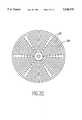
- FIG. 2cis a plan view of a chuck surface pattern over which the present invention provides a marked improvement in performance
- FIG. 3ashows the values of the average heat transfer coefficient between the wafer and the ESC (h a ) obtained for a typical ESC, referred to as ESC-1, as a function of the helium pressure (P He ) from 0 to 10 Torr and for various values of the ESC clamping voltage (V ESC ) up to 1,000 volts;
- FIG. 3bshows the values of the average heat transfer coefficient between the wafer and the ESC (h a ) obtained for another ESC, referred to as ESC-2, as a function of the helium pressure (P He ) from 0 to 10 Torr and for various values of the ESC clamping voltage (V ESC ) up to 1,000 volts;
- FIG. 5shows the behavior of h c as a function of V ESC from 400 to 1,000 volts measured on the five different ESCs in FIGS. 3a, 3b, and 4;
- FIG. 6ashows the calculated values of the heat transfer coefficient (h g ) as a function of P He for ESC-1 and ESC-2 in FIGS. 3a and 3b;
- FIG. 7shows the calculated (solid curve) and measured (data points and dashed curves) wafer temperature distributions for an ESC having the groove pattern shown in FIG. 2c.
- FIG. 8ashows a waffle type chuck surface pattern consisting of small square contacts in accordance with a preferred embodiment of the invention
- FIG. 8bshows, for purposes of a comparison with FIG. 7, the calculated (solid curve) and measured (data points and dashed curves) wafer temperature distributions for an ESC chuck having a groove pattern shown in FIG. 8a and operated under similar conditions used in deriving the data shown in FIG. 7;
- FIG. 9shows the temperature uniformity profile for the improved ESC.
- FIG. 10shows a preferred form of chuck surface pattern in accordance with the invention.
- the ESCconsisted of a ceramic (Al 2 O 3 ) body with an embedded tungsten electrode.
- the electrostatic characteristics of this chuckhave been described previously by Watanabe (see Watanabe, T. Kitabayashi, and C. Nakayama, Japan J. Appl. Phys., 33, 2145 (1992)).
- Watanabesee Watanabe, T. Kitabayashi, and C. Nakayama, Japan J. Appl. Phys., 33, 2145 (1992)
- Watanabesee Watanabe, T. Kitabayashi, and C. Nakayama, Japan J. Appl. Phys., 33, 2145 (1992)
- FIG. 1An exemplary form of a reactor in which an ECR-CVD process may be carried out is illustrated in cross-section in FIG. 1. It is to be understood that no admission is made that any portion on FIG. 1 is prior art as to the present invention, particularly since, at the level of detail contained in FIG. 1, the depiction of the electrostatic chuck could represent either a known electrostatic chuck or an electrostatic chuck in accordance with the invention. It is also to be understood that an electrostatic chuck in accordance with the invention will produce the effects of permitting both coarse and fine temperature adjustment and provide increased temperature uniformity across the surface of the wafer regardless of the process being performed or the details of any reactor which is appropriate to that process.
- reactor 100principally comprises a housing 110, 130 capable of withstanding a deep vacuum surrounded by coils for regulating magnetic fields within the housing and other devices for controlling conditions within the housing such as the reactant materials and the energy supplied thereto.
- the housingis preferably separable into upper and lower parts (110 and 130, respectively) for facilitating the positioning of a wafer on the electrostatic chuck 10 located at an upper surface of the lower portion 130.
- the remainder of the upper surface of the lower housing portion 130is preferably water cooled in a manner which is well understood in the art and not critical to the practice of the invention.
- Upper housing portion 110includes a funnel-shaped water-cooled portion 120 which determines the geometry of the upper surface of the reaction chamber formed between upper and lower housing portions 110, 130.
- the geometry of this surfaceis also not critical to the practice of the invention; simply serving to confine reactants near the wafer surface.
- Centrally located above surface 120is a plasma chamber in which high levels of energy will be imparted to the low pressure gases in the reaction chamber which will cause them to ionize. The is preferably accomplished by supplying microwave energy through a window 150.
- the dynamics of the plasma so generatedare controlled by a magnetic field generated by passing a current through coil 140 surrounding the plasma chamber.
- this fieldserves to contain the plasma to limit electron and ion flux to the walls of the plasma chamber and to limit material deposition thereon.
- magnetic fields generated by mirror and cusp coils 160serve to direct ions to the vicinity of the electrostatic chuck 10 where a wafer will be located during processing.
- Reactant materialsare introduced into the reactor at appropriate locations by passages 170 and 180.
- Temperature of the waferis preferably monitored by a temperature probe 190, preferably located at approximately the center of a radius of the chuck 10.
- Electrostatic (e.g. DC) and RF bias, coolant gas and liquid coolant for the chuckare also supplied from the back of the lower housing portion 130 as will be discussed in greater detail with reference to FIGS. 2a, 2b and 2c.
- FIGS. 2a, 2b and 2cThe geometry of the electrostatic chuck with a wafer is depicted in greater detail in FIGS. 2a, 2b and 2c. It is to be understood that the invention does not rely on the details of the internal structure of the electrostatic chuck and no admission is made that any portion of FIGS. 2a-2c is prior art in regard to the present invention.
- the depictions in FIGS. 2a-2care not to scale and are intended to provide enhanced clarity in the discussion of the operation of electrostatic chucks, in general, as well as the problems of temperature uniformity and control previously encountered in using electrostatic chucks.
- the electrostatic chuck 10includes a cooling plate 12, preferably of copper (although other materials of good thermal conductivity can be used), located at the rear thereof or at least a convenient distance from the front surface 14 of the ESC.
- Cooling plate 12preferably includes a manifold or channel in which water or other cooling liquid may be circulated, as indicated by coolant inlet 12' and outlet 12".
- the water-cooled plateis preferably maintained at 70° C. but this temperature may be varied in dependence on the requirements of heat removal in a particular process. Further structure may be employed as desired behind the cooling plate 12 for immobilization or manipulation of the chuck or for other purposes without affecting the operation of the heat transfer structures near the front surface 14 of the ESC.
- the front surface 14 of the ESCis preferably formed of a dielectric layer provided with grooves 16 (which may be in fluid communication with each other as shown in FIG. 2c) for the circulation of a gas in contact with the back side of the wafer 18 at a relatively static pressure when wafer 18 is in contact with front surface 14 of ESC 10.
- the gasis provided to grooves 16 through one or more passages 20.
- gas provided in grooves 16is often at higher pressure than the pressure at which a semiconductor process is carried out in the reactor chamber and some leakage of gas will usually occur, requiring some flow of gas to maintain a static pressure. This flow may also contribute to heat transfer from the wafer and the chuck but will generally be small. If leakage is sufficient for the gas flow rate intended, no outlet for the gas need be provided. However, one or more further passages 20 could be provided as outlets in order to support the gas flow rate desired.
- an electrodepreferably formed from tungsten (for heat tolerance and thermal expansion characteristics) is provided as closely as possible to surface 14 below the bottoms of grooves 16.
- electrode 22could be provided at a shallower depth and grooves 16 cut therethrough to form a mesh-like pattern.
- such a structurerequires electrical continuity to all portions of the mesh (which may complicate the groove and gas flow pattern) while reducing the area of the electrode and, in accordance with a reduced contact surface ratio following the principles of the invention, would cause a greater reduction in attractive force applied to the wafer than increasing the electrode depth to a location below the grooves 16.
- a shallower depth than the groove depthcould cause exposure of the tungsten during chamber cleaning and provide a mechanism for damage to the ESC.
- a thick electrode of tungsten or aluminumcould be provided and grooves in accordance with the invention cut directly in the face of the electrode to a depth less than the electrode thickness. Then the entire face surface of the ESC could be covered with a protective insulating coating layer such as aluminum oxide. This alternative method of formation of the ESC prevents any inadvertent exposure of metal within the reactor.
- a uniform electrostatic potentialis applied between the wafer and the ESC by applying a DC bias along with any radio frequency bias required by a particular semiconductor wafer processing operation to the tungsten electrode 22 to produce an attractive force between the wafer and the chuck.
- a reduction in the electrostatic potential and attractive forceoccurs near the edge of the wafer in the overhang region 24.
- the diameter of an ESCshould be slightly less than the wafer diameter in CVD applications, in order to shield the ESC surface from the deposition process.
- the magnitude of the electrostatically developed attractive forceis not critical to the practice of the invention, although temperature control is achieved in accordance therewith, as will be discussed below.
- the attractive forcemust be sufficient to immobilize the wafer 18 against surface 14 of ESC 10 even when static pressure in grooves 16 is significantly higher than the ambient semiconductor process pressure in whatever semiconductor processing apparatus is employed for a particular processing operation.
- the surface of the ESCis patterned by machining grooves into the ceramic, creating "contact" regions 14', where the Si wafer and ESC form an intimate contact, and "grooved" regions, where the Si wafer and ESC have a fixed separation to accommodate a gas at a relatively constant static pressure.
- Two types of surface patternswere analyzed and used for experimental verification: a reference "ring” pattern type consisting of circumferential contacts, as shown in FIG. 2c, and a waffle pattern type consisting of small square contacts in accordance with a preferred embodiment of the invention, shown in FIG. 10.
- the grooves in the chuckwere 13 ⁇ m deep for both ESC surface patterns.
- the grooveswere approximately 0.6 cm wide and separated by contact regions of about 0.66 cm in the radial dimension.
- the rectangular contact padswere 0.3 cm wide separated by grooves having a slightly greater width for the waffle pattern.
- the surface roughness of the ESC facewas nominally 0.2 to 0.5 microns and it has been discovered by the inventors that the wafer temperature was proportional to the surface roughness (the greater the roughness, the higher the wafer temperature, with all else being equal) in much the same manner that changing the nominal contact area fraction (e.g. the area of the chuck face 14 less the area of grooves 16, divided by the area of the chuck face, or the area of areas 14' divided by area 14).
- this surface roughnesswas much greater than the surface roughness of a polished Si wafer and about the same as an unpolished Si wafer (which is about 0.3 ⁇ m).
- Changing the nominal contact area fraction together with a nominal surface roughnesswas thus determined to be a good way to manufacture chucks for operation at different wafer temperature ranges (e.g., a chuck with a lower contact area fraction would result in a higher wafer temperature for a given operation). That is, in accordance with the invention, choosing a contact area fraction as a function of both nominal contact area fraction and nominal surface roughness determined the nominal wafer temperature for a given set of reaction conditions.
- an RF power density of 7 watts/cm 2was applied to the wafer.
- the pressure of the He between the ESC and wafer (P He ), and the ESC clamping voltage (V ESC ),are varied between 0-10 Torr and 400-1,000 volts, respectively.
- the average wafer temperaturewas controlled from 180° C. to 450° C.
- the wafer temperature and temperature uniformitywere determined while operating the reactor under deposition-like conditions, with an Ar plasma substituted for the reactive gas mixture.
- the steady-state wafer temperaturewas measured in real-time at one location about mid-radius on the wafer using a fiber optic infrared detector located behind the wafer.
- Wafer temperature uniformitywas determined using a mapping technique which relies on a change in resistivity of the film (although any other measurable property of the film such as optical properties, thickness, etc. could theoretically be used) with time-temperature exposure.
- This techniquemeasures the temperature with a spatial resolution of ⁇ 0.2 cm and has a relative temperature sensitivity of ⁇ 1° C. and an absolute accuracy of ⁇ 7° C.
- the temperature of the wafer during CVD depositionis a function of 1.) the ESC clamping voltage, V ESC , 2.) the pressure of the He between the ESC and wafer, P He , 3.) the ion flux incident on the surface of the wafer, F i , 4.) the temperature on the backside of the ESC, T ESC , 5.) the surface roughness of the chuck, and 6.) the thermal transport of heat from the top surface of the silicon wafer to the bottom of the ESC. Because of the relatively high thermal conductivity of the Si wafer and the ESC compared with the interface region between the wafer and the ESC, a large temperature gradient occurs near the wafer/ESC interface.
- a value for the average heat transfer coefficient between the wafer and the ESC, h ais estimated by measuring the temperature T W (using temperature probe 190, as shown in FIG. 1 ) of the wafer at mid-radius during the deposition-like conditions for various values of the ESC clamping voltage V ESC , and He supply pressures P He . This measured temperature is assumed to represent an average temperature of the wafer.
- FIGS. 3a and 3bshow the values of h a obtained for two ESCs as a function of P He from 0 to 10 Torr and for various values of V ESC up to 1,000 volts.
- the average heat transfer coefficient h ais found to be linear with respect to P He . This behavior is consistent with Knudsen's theory of heat conduction between parallel plates where the total heat transfer is linear with pressure as long as the plate separation is small with respect to the mean tree path in the gas.
- Change of V ESCcauses a relatively linear vertical shift of the linear relationship between average heat transfer coefficient h a and gas pressure P He .
- the average heat transfer coefficient h ais about 0.024 watts/cm 2 ⁇ °K, and the temperature of the wafer is ⁇ 400° C.
- the inventorshave also discovered that, because the surface roughness can differ between various ESCs (e.g., ESC-1 and ESC-2), the heat transfer from the wafer to the ESC can vary, resulting in a different wafer temperature for the same operating conditions of P He and V ESC . If controlling the surface finish of the ESC is problematic, wafer temperature will change from chuck to chuck. In addition, changing the area fraction of the ESC surface which is in intimate contact with the wafer (X c ) will also change the heat transfer properties and alter the temperature of the Si wafer.
- the surface roughness on chucks ESC-4 and ESC-5are similar to that of ESC-1.
- the surface of ESC-3is considerably smoother than all the other chucks and thus has the highest value of h a .
- the value of h ais found to be nearly linear with respect to P He .
- the slight decrease from linearity at the higher pressuresis believed to be due to the competition between the helium pressure, which tends to separate the wafer from the ESC and the electrostatic potential which forces them together. This effect is particularly evident on chuck ESC-3.
- Controlling the surface finish of the ESCis therefore considered to be important to reducing wafer temperature variations from chuck to chuck and to obtain consistent performance in the practice of the invention.
- changing either the nominal contact area fraction on the ESC surface which is in intimate contact with wafer, or varying the surface roughness in a controlled way,will alter the heat transfer properties of the chuck and change the temperature of the wafer.
- X cis the localized area fraction of the ESC which is in intimate contact with the wafer.
- the value of h cis a function of V ESC , P He , and the surface roughness of the ESC.
- the value of h gdepends only upon P He and the gas itself (i.e. argon gas would result in a different h g for the same pressure).
- FIG. 5shows the behavior of h c for the five different chucks described in FIGS. 3a, 3b, and 4.
- the value of h cis lowest for the ESC with the greatest surface roughness (ESC-2) and highest for the ESC with the least surface roughness (ESC-3).
- the value of h cis found to increase monotonically with increasing values of V ESC which is believed to be due to an increase in the intimacy of contact between the wafer and the ESC (e.g.
- the value of h cis somewhat more strongly dependent upon the surface roughness of the ESC than the value of V ESC .
- V ESC800 volts
- the values of h ccould be varied by a factor of 2 ⁇ , from a value of 0.054 to 0.11 watts/cm 2 ⁇ °K by changing the surface roughness of the chucks, while the value of h c only increased by a factor of 1.6 ⁇ , from a value of 0.047 to 0.079 watts/cm 2 ⁇ K when increasing V ESC from 500 to 1,000 volts. It is for this reason that control of chuck surface roughness is preferred for establishing a nominal wafer temperature range in a given semiconductor processing operation for a given nominal contact area fraction of the groove pattern of the ESC, as alluded to above.
- FIG. 6ashows the calculated values of h g as a function of P He for ESC-1 and ESC-2.
- the values of h gare plotted for all three values (e.g. 500 V, 700 V, 900 V) of V ESC , since there is no distinguishable variation in h g as a function of V ESC .
- the model systemconsists of three layers: the Si wafer, the ESC, and an interfacial layer separating the wafer from the ESC which was developed as discussed above. This interfacial layer represents the contact region between the wafer and the ESC and contains the details of the geometry of the surface pattern on the ESC.
- the interfacial layer between the top surface of the ESC and the backside of the wafercan be thought of in terms of a heat transfer coefficient h, whose value is spatially modulated in accordance with the groove pattern machined into the surface of the ESC.
- hh c +h g at the "contact” regions
- hh g at the "grooved” regions.
- the value of hwas modified over the outer contact region at the edge of the ESC.
- He pressurefrom the static pressure P He at inside boundary of the final contact region to a pressure on the order of 1 mTorr at the outside boundary of the contact region, at high vacuum corresponding to ECR-CVD process conditions
- the value of h gwas either linearly reduced to zero between the inner and outer edge of the final contact region to represent the reduction in He pressure, or a step function was imposed on the value of h g , reducing its value to zero at a distance near the edge of the ESC where the tungsten electrode terminates. Both methods were found to give satisfactory results.
- k a (T)is the thermal conductivity of either the wafer or the ESC and T is the temperature
- vis an operator such that ##EQU2## where a x is the unit vector in the x direction, a y is the unit vector in the y direction, and a z is the unit vector in the z direction.
- Equation (3)The following boundary conditions are imposed on the solution of Equation (3):
- F iA uniform flux of energy, F i , is applied to the top surface of the wafer. This energy is caused by ion bombardment from the plasma and represents 80% of the applied RF power during the oxide deposition process;
- a constant temperature of 70° C.is maintained on the back surface of the ESC. This temperature is fixed by the temperature of the water flowing through the plate on which the ESC is mounted. The temperature in the body of the ESC is calculated along with the temperature of the wafer surface;
- T wb (r) and T ef (r)are the temperatures on the back surface of the Si wafer and the front surface of the ESC at position r, respectively. Special consideration is given to the contact region at the edge of the ESC as discussed above.
- Radiation loss and heat loss to the walls of the reactorare not included in the model.
- the radiation loss per unit areais 0.4 watts/cm 2 , using an emissivity of 0.4. This represents only ⁇ 7% of the incident flux of heat to the wafer and can be neglected to first order.
- the loss of heat to the reactor walls due to conduction and convectionwere likewise ignored due to the low pressure of ⁇ 1 mTorr and low flow rates used during the deposition process.
- the temperature distributionis calculated in both the wafer and in the ESC by solving Eqs. (2) and (3) using finite element technique (see FIDAP CFD Code, commercially available from Fluid Dynamics International, Evanston, Ill.). Of particular importance is the calculated temperature distribution at the surface of the wafer.
- FIGS. 7 and 8bshow the calculated (solid curve) and measured (data points and dashed curves) wafer temperature distributions for two electrostatic chucks with different surface patterns operated under similar conditions.
- the data in FIG. 7was obtained from an ESC having a circumferential "contact" pattern similar to FIG. 2c while that in FIG. 8b was obtained from an ESC having waffle "contact” pattern similar to that shown in FIG. 10.
- the radius of both chucksis 0.5 cm smaller than the wafer. Because of the relatively high thermal conductivity of the wafer and ESC compared to the interfacial region between the wafer and the ESC, most of the temperature drop between the top wafer surface and the bottom of the ESC occurs at the interface between the wafer and the ESC. Under all conditions studied, the temperature drop within the bulk of the ESC was ⁇ 10° C.
- the calculated temperature distribution shown in FIG. 7initially increases with increasing radius, gradually decreases before rising again near the edge of the wafer.
- the reduction in temperature at the center of the waferis caused by the large "contact" region at the center of the ESC which serves as an enhanced heat sink.
- the decrease in temperature with increasing radiusis due to an increase in the area fraction of the "contact” regions with increasing radius and to a wide diameter "contact” pad at the edge of the ESC.
- the temperature rise at the edge of the waferis due to the reduction in the heat transport at the edge of the wafer which overhangs the ESC.
- the small temperature oscillation which occurs every approximately 1.2 cmdirectly corresponds to the periodicity of "contact” and "grooved” regions on the surface of the ESC indicating that grooves and contact regions are too wide relative to the thermal conductivity of the wafer and in consideration of the relative heat transfer contributions of the contact regions of the chuck and the gas contained in the grooves.
- the periodicity of the grooves to avoid the oscillations observed in FIG. 7 for a known ESC surface patterndepends on many factors and becomes more critical as wafer thickness is reduced, it has been found by the inventors that for silicon wafers a periodicity of less than ten times the wafer thickness provides uniformly acceptable results.
- Periodicity of the groove pattern for wafers of other semiconductor materialscan be scaled from this guideline based on relative thermal conductivity.)
- the wafer temperature distributionwas measured along a diameter of the wafer.
- the two experimental curvesrepresent this data. As can be seen, the model captures the basic features of the measured temperature distribution.
- the predicted temperature of the wafer having a contact or groove pattern similar to that depicted in FIG. 8ais shown in FIG. 8b.
- This temperatureinitially decreases gradually as a function of radius up to a radius of about 6 cm, then the temperature decreases sharply towards the edge of the wafer.
- the sharp decrease in temperatureis due to the enhanced heat sink caused by the large contact region at the edge of the ESC. Because of the smaller spacing between "contact" regions (0.3 cm vs. 0.6 cm in FIG. 7) wafer temperature oscillations are not observed in the predicted or the measured temperature profiles.
- the size of the final, outer, “contact” regionneeds to be chosen to better balance the heat transfer from the edge of the wafer. That is, to remove the energy incident on the area which is not in contact with the chuck where the wafer edge overhangs the outer perimeter of the chuck face which would otherwise increase the temperature of adjacent areas of the wafer.
- the central area of the wafer within the inner boundary of that annular contact regionis unaffected by the "excess" energy incident on the overhang of the wafer and which does not have a corresponding area of the chuck face.
- the optimum width of the annular contact regionwill increase (or decrease) with increasing (or decreasing) wafer overhang since the "excess" incident energy will vary with the area of the overhang.
- the outer contact regioncan all be made too large, particularly in the case of the preferred embodiment of the invention in which the ESC is preferably sized to reduce wafer overhang relative to the present practice.
- the chuckhas a larger radius less than 1.0 mm smaller than the wafer diameter) to reduce overhang (and the outer annular region width has been optimized for this overhang) and the rise in temperature over the outer portion of the wafer is held to about 30° C.
- the periodicity of the waffle patternhas also been optimized to wafer thickness to avoid the oscillations observed in FIG. 7 for the known ESC surface pattern. Again, the model captures the basic features of the measured temperature distribution and good agreement is obtained between the measured and predicted temperature distributions. There are no free parameters in the temperature model.
- the nominal (local) contact area fraction of the outer annular contact regionis equal to one but that the effective contact area fraction is affected by surface roughness and the clamping voltage, as described above.
- h cis substantially greater than h g and that h g is unaffected by clamping voltage and varies only with gas pressure. Therefore, clamping voltage can also be used as a coarse adjustment of the balancing of the "excess" incident energy or heat and a fine adjustment can be provided by adjustment of gas pressure because of the difference in contact area fraction between the central and outer, annular regions of the ESC face.
- the width of the outer, annular contact regionneed only be of a nominal width which will allow a balance to be achieved within acceptable ranges of values of clamping voltage and gas pressures.
- a preferred working value of the width of the outer, annular region which will allow "excess" energy to be balancedis approximately 2.0 to 2.5 times the nominal overhang dimension.
- the surface roughness of the outer, annular portion or rimneed not be the same as the surface roughness of the central portion defined by the groove pattern or even constant over the width of the outer, annular portion.
- the results from these modelsindicate that once the heat transfer coefficients of the ESC have been determined, good agreement can be obtained between the measured and predicted wafer temperature uniformity.
- the numerical modelcan be used to provide insight into the effects of the operating and design parameters of the ESC on the wafer temperature uniformity.
- the modelscan also be used as a design tool to improve the geometry of the ESC surface pattern to reduce the nonuniformities in temperature at the wafer surface.
- the performance of chuck surface patternscan be readily optimized for a particular heat flux and wafer temperature by simulating surface patterns having different widths of the outer contact region or annulus in accordance with the above discussion of effective ESC radius.
- Such a simulation and optimization process for the heat flux appropriate to an ECR-CVD processresults in the preferred pattern shown in FIG. 10.
- This preferred patternhas a waffle-type pattern formed by a network of intersecting grooves having a width and spacing to produce a constant nominal contact area fraction in the range of 20% to 40% and an outer, annular region having a width of approximately 6 mm; the outer boundary of which is located at a radius which is approximately 0.1 cm less than the radius of a wafer to be held.
- the width of the outer, annular regionis approximately 6.0 to 7.0 min.
- FIG. 9The simulated temperature profile across the wafer obtained with the chuck surface pattern of FIG. 10 is shown in FIG. 9, in which the model was used to predict the wafer temperature uniformity with different widths of the outer contact region. It was found that the wafer temperature uniformity could be improved by increasing the inner diameter of the outer contact region, thus reducing the heat transport between the wafer and the ESC at the edge of the wafer. Further improvements were obtained by having the total radius of the ESC closer to that of the wafer, thus minimizing the "excess" heat which must be transferred to the ESC through the annular contact region.
- FIG. 9shows the measured wafer temperature profile obtained for an ESC having the waffle "contact" pattern and optimized to produce an average wafer temperature of 340° C.
- the wafer temperatureis essentially flat over the inner 6 cm radius then gradually increases by only 30° C. at the edge of the wafer.
- the increase in the wafer temperature near the edge of the waferis due primarily to the 0.1 cm overhang of the wafer, which represents 2% of the area of the wafer.
- the chuck surface pattern in accordance with the inventionprovides substantially improved temperature uniformity across the surface of a wafer held by an electrostatic chuck during semiconductor processing operations. Further, quantification and characterization of the wafer-ESC interface allows the nominal wafer surface temperature range to be determined by the surface roughness of the contact portions of the chuck and reducing the contact area fraction as much as possible consistent with the heat flux which must be conducted across the interface. A coarse adjustment of wafer surface temperature may then be accomplished by variation of the electrostatic voltage used to hold the wafer against the chuck and fine temperature adjustment can be made by variation of the static pressure of gas contained in grooves in the chuck surface.
Landscapes
- Engineering & Computer Science (AREA)
- Physics & Mathematics (AREA)
- Condensed Matter Physics & Semiconductors (AREA)
- General Physics & Mathematics (AREA)
- Manufacturing & Machinery (AREA)
- Computer Hardware Design (AREA)
- Microelectronics & Electronic Packaging (AREA)
- Power Engineering (AREA)
- Container, Conveyance, Adherence, Positioning, Of Wafer (AREA)
- Jigs For Machine Tools (AREA)
Abstract
Description
h.sub.a =X.sub.c h.sub.c +h.sub.g (2)
v·k.sub.a (T)∇T=0 (3)
q(r)=h(r)(T.sub.wb (r)-T.sub.ef (r)) (4)
Claims (21)
Priority Applications (4)
| Application Number | Priority Date | Filing Date | Title |
|---|---|---|---|
| US08/277,552US5548470A (en) | 1994-07-19 | 1994-07-19 | Characterization, modeling, and design of an electrostatic chuck with improved wafer temperature uniformity |
| US08/480,108US5675471A (en) | 1994-07-19 | 1995-06-07 | Characterization, modeling, and design of an electrostatic chuck with improved wafer temperature uniformity |
| EP95480079AEP0693774A2 (en) | 1994-07-19 | 1995-06-22 | Characterization, modeling, and design of an electrostatic chuck with improved wafer temperature uniformity |
| JP17641695AJP3437883B2 (en) | 1994-07-19 | 1995-07-12 | Electrostatic chuck, electrostatic chuck system, and method for processing semiconductor wafer |
Applications Claiming Priority (1)
| Application Number | Priority Date | Filing Date | Title |
|---|---|---|---|
| US08/277,552US5548470A (en) | 1994-07-19 | 1994-07-19 | Characterization, modeling, and design of an electrostatic chuck with improved wafer temperature uniformity |
Related Child Applications (1)
| Application Number | Title | Priority Date | Filing Date |
|---|---|---|---|
| US08/480,108Continuation-In-PartUS5675471A (en) | 1994-07-19 | 1995-06-07 | Characterization, modeling, and design of an electrostatic chuck with improved wafer temperature uniformity |
Publications (1)
| Publication Number | Publication Date |
|---|---|
| US5548470Atrue US5548470A (en) | 1996-08-20 |
Family
ID=23061359
Family Applications (2)
| Application Number | Title | Priority Date | Filing Date |
|---|---|---|---|
| US08/277,552Expired - LifetimeUS5548470A (en) | 1994-07-19 | 1994-07-19 | Characterization, modeling, and design of an electrostatic chuck with improved wafer temperature uniformity |
| US08/480,108Expired - Fee RelatedUS5675471A (en) | 1994-07-19 | 1995-06-07 | Characterization, modeling, and design of an electrostatic chuck with improved wafer temperature uniformity |
Family Applications After (1)
| Application Number | Title | Priority Date | Filing Date |
|---|---|---|---|
| US08/480,108Expired - Fee RelatedUS5675471A (en) | 1994-07-19 | 1995-06-07 | Characterization, modeling, and design of an electrostatic chuck with improved wafer temperature uniformity |
Country Status (3)
| Country | Link |
|---|---|
| US (2) | US5548470A (en) |
| EP (1) | EP0693774A2 (en) |
| JP (1) | JP3437883B2 (en) |
Cited By (45)
| Publication number | Priority date | Publication date | Assignee | Title |
|---|---|---|---|---|
| US5675471A (en)* | 1994-07-19 | 1997-10-07 | International Business Machines Corporation | Characterization, modeling, and design of an electrostatic chuck with improved wafer temperature uniformity |
| US5745331A (en)* | 1994-01-31 | 1998-04-28 | Applied Materials, Inc. | Electrostatic chuck with conformal insulator film |
| US5761023A (en)* | 1996-04-25 | 1998-06-02 | Applied Materials, Inc. | Substrate support with pressure zones having reduced contact area and temperature feedback |
| US5801915A (en)* | 1994-01-31 | 1998-09-01 | Applied Materials, Inc. | Electrostatic chuck having a unidirectionally conducting coupler layer |
| US5812362A (en)* | 1996-06-14 | 1998-09-22 | Applied Materials, Inc. | Method and apparatus for the use of diamond films as dielectric coatings on electrostatic chucks |
| US5946184A (en)* | 1996-09-19 | 1999-08-31 | Hitachi, Ltd. | Electrostatic chuck, and method of and apparatus for processing sample |
| US5952060A (en)* | 1996-06-14 | 1999-09-14 | Applied Materials, Inc. | Use of carbon-based films in extending the lifetime of substrate processing system components |
| US6028762A (en)* | 1996-01-31 | 2000-02-22 | Kyocera Corporation | Electrostatic chuck |
| US6056850A (en)* | 1996-07-12 | 2000-05-02 | Micron Technology, Inc. | Apparatus for improving the performance of a temperature-sensitive etch process |
| US6084763A (en)* | 1996-06-21 | 2000-07-04 | Sony Corporation | Method of holding wafer, method of removing wafer and electrostatic chucking device |
| US6134096A (en)* | 1995-09-06 | 2000-10-17 | Ngk Insulators, Ltd. | Electrostatic chuck |
| US6151203A (en)* | 1998-12-14 | 2000-11-21 | Applied Materials, Inc. | Connectors for an electrostatic chuck and combination thereof |
| US6373679B1 (en) | 1999-07-02 | 2002-04-16 | Cypress Semiconductor Corp. | Electrostatic or mechanical chuck assembly conferring improved temperature uniformity onto workpieces held thereby, workpiece processing technology and/or apparatus containing the same, and method(s) for holding and/or processing a workpiece with the same |
| US6399143B1 (en) | 1996-04-09 | 2002-06-04 | Delsys Pharmaceutical Corporation | Method for clamping and electrostatically coating a substrate |
| US6628503B2 (en) | 2001-03-13 | 2003-09-30 | Nikon Corporation | Gas cooled electrostatic pin chuck for vacuum applications |
| US6643115B2 (en)* | 2001-02-27 | 2003-11-04 | Kyocera Corporation | Electrostatic chuck |
| US20040040665A1 (en)* | 2002-06-18 | 2004-03-04 | Anelva Corporation | Electrostatic chuck device |
| US20040233608A1 (en)* | 2003-05-21 | 2004-11-25 | Tokyo Electron Limited Of Tbs Broadcast Center | Apparatus and methods for compensating plasma sheath non-uniformities at the substrate in a plasma processing system |
| US7033444B1 (en)* | 1999-06-21 | 2006-04-25 | Tokyo Electron Limited | Plasma processing apparatus, and electrode structure and table structure of processing apparatus |
| US20060209490A1 (en)* | 2005-02-24 | 2006-09-21 | Kyocera Corporation | Electrostatic chuck and wafer holding member and wafer treatment method |
| US20070030621A1 (en)* | 2005-08-05 | 2007-02-08 | Lam Research Corporation | Method and apparatus for chuck thermal calibration |
| CN100419989C (en)* | 2005-12-05 | 2008-09-17 | 北京北方微电子基地设备工艺研究中心有限责任公司 | Static chuck |
| US20100055879A1 (en)* | 2008-08-29 | 2010-03-04 | Renesas Technology Corp. | Method for manufacturing a semiconductor device |
| US20110186545A1 (en)* | 2010-01-29 | 2011-08-04 | Applied Materials, Inc. | Feedforward temperature control for plasma processing apparatus |
| US20110228439A1 (en)* | 2010-03-17 | 2011-09-22 | Tokyo Electron Limited | Substrate mounting and demounting method |
| US20120132397A1 (en)* | 2010-06-08 | 2012-05-31 | Applied Materials, Inc. | Temperature control in plasma processing apparatus using pulsed heat transfer fluid flow |
| WO2014113244A1 (en)* | 2013-01-18 | 2014-07-24 | Applied Materials, Inc. | Temperature management of aluminium nitride electrostatic chuck |
| TWI467691B (en)* | 2008-10-15 | 2015-01-01 | Creative Tech Corp | Electrostatic chuck and its manufacturing method |
| US8941969B2 (en) | 2012-12-21 | 2015-01-27 | Applied Materials, Inc. | Single-body electrostatic chuck |
| CN105321848A (en)* | 2014-05-30 | 2016-02-10 | Icd株式会社 | Contact geometry for processing object in chamber, electrostatic chuck and manufacturing method thereof |
| US9639097B2 (en) | 2010-05-27 | 2017-05-02 | Applied Materials, Inc. | Component temperature control by coolant flow control and heater duty cycle control |
| US9666466B2 (en) | 2013-05-07 | 2017-05-30 | Applied Materials, Inc. | Electrostatic chuck having thermally isolated zones with minimal crosstalk |
| US9669653B2 (en) | 2013-03-14 | 2017-06-06 | Applied Materials, Inc. | Electrostatic chuck refurbishment |
| US9685356B2 (en) | 2012-12-11 | 2017-06-20 | Applied Materials, Inc. | Substrate support assembly having metal bonded protective layer |
| US20180033672A1 (en)* | 2016-07-27 | 2018-02-01 | Lam Research Corporation | Substrate support with increasing areal density and corresponding method of fabricating |
| US9887121B2 (en) | 2013-04-26 | 2018-02-06 | Applied Materials, Inc. | Protective cover for electrostatic chuck |
| US9916998B2 (en) | 2012-12-04 | 2018-03-13 | Applied Materials, Inc. | Substrate support assembly having a plasma resistant protective layer |
| US10020218B2 (en) | 2015-11-17 | 2018-07-10 | Applied Materials, Inc. | Substrate support assembly with deposited surface features |
| US10274270B2 (en) | 2011-10-27 | 2019-04-30 | Applied Materials, Inc. | Dual zone common catch heat exchanger/chiller |
| US10679884B2 (en) | 2015-02-23 | 2020-06-09 | M Cubed Technologies, Inc. | Film electrode for electrostatic chuck |
| CN111725127A (en)* | 2019-03-19 | 2020-09-29 | 日本碍子株式会社 | Chip carrying device and manufacturing method thereof |
| US10896837B2 (en)* | 2018-10-01 | 2021-01-19 | Lam Research Corporation | Ceramic foam for helium light-up suppression |
| US11004716B2 (en)* | 2016-10-31 | 2021-05-11 | Samsung Electronics Co., Ltd. | Electrostatic chuck assembly and semiconductor manufacturing apparatus including the same |
| CN112885738A (en)* | 2020-09-03 | 2021-06-01 | 天虹科技股份有限公司 | Wafer fixing mechanism and wafer pre-cleaning machine station using same |
| CN113130286A (en)* | 2019-12-31 | 2021-07-16 | 中微半导体设备(上海)股份有限公司 | Aging treatment method for electrostatic chuck |
Families Citing this family (38)
| Publication number | Priority date | Publication date | Assignee | Title |
|---|---|---|---|---|
| US5810933A (en)* | 1996-02-16 | 1998-09-22 | Novellus Systems, Inc. | Wafer cooling device |
| GB9711273D0 (en)* | 1997-06-03 | 1997-07-30 | Trikon Equip Ltd | Electrostatic chucks |
| US5903428A (en)* | 1997-09-25 | 1999-05-11 | Applied Materials, Inc. | Hybrid Johnsen-Rahbek electrostatic chuck having highly resistive mesas separating the chuck from a wafer supported thereupon and method of fabricating same |
| US6482747B1 (en)* | 1997-12-26 | 2002-11-19 | Hitachi, Ltd. | Plasma treatment method and plasma treatment apparatus |
| US6561796B1 (en) | 1999-09-07 | 2003-05-13 | Novellus Systems, Inc. | Method of semiconductor wafer heating to prevent bowing |
| JP4209057B2 (en)* | 1999-12-01 | 2009-01-14 | 東京エレクトロン株式会社 | Ceramic heater, substrate processing apparatus and substrate processing method using the same |
| WO2002017384A1 (en)* | 2000-08-23 | 2002-02-28 | Applied Materials, Inc. | Electrostatic chuck temperature control method and system |
| TWI272689B (en)* | 2001-02-16 | 2007-02-01 | Tokyo Electron Ltd | Method and apparatus for transferring heat from a substrate to a chuck |
| JP4493251B2 (en)* | 2001-12-04 | 2010-06-30 | Toto株式会社 | Electrostatic chuck module and substrate processing apparatus |
| US20040079289A1 (en)* | 2002-10-23 | 2004-04-29 | Kellerman Peter L. | Electrostatic chuck wafer port and top plate with edge shielding and gas scavenging |
| USD491206S1 (en) | 2002-12-20 | 2004-06-08 | Ngk Spark Plug Co., Ltd. | Electrostatic chuck |
| EP1458019A3 (en)* | 2003-03-13 | 2005-12-28 | VenTec Gesellschaft für Venturekapital und Unternehmensberatung | Mobile transportable electrostatic substrate holders |
| US7033443B2 (en)* | 2003-03-28 | 2006-04-25 | Axcelis Technologies, Inc. | Gas-cooled clamp for RTP |
| US20040187787A1 (en)* | 2003-03-31 | 2004-09-30 | Dawson Keith E. | Substrate support having temperature controlled substrate support surface |
| US20040221959A1 (en) | 2003-05-09 | 2004-11-11 | Applied Materials, Inc. | Anodized substrate support |
| US8372205B2 (en)* | 2003-05-09 | 2013-02-12 | Applied Materials, Inc. | Reducing electrostatic charge by roughening the susceptor |
| US7846254B2 (en)* | 2003-05-16 | 2010-12-07 | Applied Materials, Inc. | Heat transfer assembly |
| JP4268450B2 (en)* | 2003-05-23 | 2009-05-27 | キヤノン株式会社 | Large glass substrate adsorption device for display |
| US7993460B2 (en)* | 2003-06-30 | 2011-08-09 | Lam Research Corporation | Substrate support having dynamic temperature control |
| JP3894562B2 (en)* | 2003-10-01 | 2007-03-22 | キヤノン株式会社 | Substrate adsorption apparatus, exposure apparatus, and device manufacturing method |
| US7869184B2 (en)* | 2005-11-30 | 2011-01-11 | Lam Research Corporation | Method of determining a target mesa configuration of an electrostatic chuck |
| US8173228B2 (en)* | 2006-01-27 | 2012-05-08 | Applied Materials, Inc. | Particle reduction on surfaces of chemical vapor deposition processing apparatus |
| US7501605B2 (en)* | 2006-08-29 | 2009-03-10 | Lam Research Corporation | Method of tuning thermal conductivity of electrostatic chuck support assembly |
| US20080131622A1 (en)* | 2006-12-01 | 2008-06-05 | White John M | Plasma reactor substrate mounting surface texturing |
| JP5295515B2 (en)* | 2007-03-30 | 2013-09-18 | 東京エレクトロン株式会社 | Surface treatment method for mounting table |
| US7649729B2 (en)* | 2007-10-12 | 2010-01-19 | Applied Materials, Inc. | Electrostatic chuck assembly |
| US7777160B2 (en)* | 2007-12-17 | 2010-08-17 | Momentive Performance Materials Inc. | Electrode tuning method and apparatus for a layered heater structure |
| JP5184188B2 (en)* | 2008-04-09 | 2013-04-17 | 株式会社ニューフレアテクノロジー | Electron beam drawing apparatus and positional deviation correction method |
| US20110068084A1 (en)* | 2008-07-10 | 2011-03-24 | Canon Anelva Corporation | Substrate holder and substrate temperature control method |
| US20110256810A1 (en)* | 2008-12-25 | 2011-10-20 | Takahiro Nanba | Method of manufacturing chuck plate for use in electrostatic chuck |
| US8486726B2 (en) | 2009-12-02 | 2013-07-16 | Veeco Instruments Inc. | Method for improving performance of a substrate carrier |
| JP5454803B2 (en)* | 2010-08-11 | 2014-03-26 | Toto株式会社 | Electrostatic chuck |
| JP5510411B2 (en)* | 2010-08-11 | 2014-06-04 | Toto株式会社 | Electrostatic chuck and method for manufacturing electrostatic chuck |
| JP6552346B2 (en)* | 2015-09-04 | 2019-07-31 | 東京エレクトロン株式会社 | Substrate processing equipment |
| KR20180093966A (en)* | 2015-12-10 | 2018-08-22 | 아이오니어 엘엘씨 | Apparatus and method for determining parameters of a process operation |
| KR102140725B1 (en)* | 2018-01-22 | 2020-08-04 | 상구정공(주) | Substrate supporting apparatus and Manufacturing method thereof |
| US20230187250A1 (en)* | 2021-12-14 | 2023-06-15 | Applied Materials, Inc. | Wafer to baseplate arc prevention using textured dielectric |
| US20230294208A1 (en)* | 2022-03-21 | 2023-09-21 | Applied Materials, Inc. | Electrostatic chuck with laser-machined mesas |
Citations (19)
| Publication number | Priority date | Publication date | Assignee | Title |
|---|---|---|---|---|
| US4261762A (en)* | 1979-09-14 | 1981-04-14 | Eaton Corporation | Method for conducting heat to or from an article being treated under vacuum |
| US4656601A (en)* | 1984-10-29 | 1987-04-07 | United Technologies Corporation | Large bandwidth saw adaptive processor arrangement |
| US4680061A (en)* | 1979-12-21 | 1987-07-14 | Varian Associates, Inc. | Method of thermal treatment of a wafer in an evacuated environment |
| JPH01251735A (en)* | 1988-03-31 | 1989-10-06 | Toshiba Corp | electrostatic chuck device |
| EP0357424A2 (en)* | 1988-09-02 | 1990-03-07 | Canon Kabushiki Kaisha | A wafer supporting apparatus |
| US4931135A (en)* | 1987-12-25 | 1990-06-05 | Tokyo Electron Limited | Etching method and etching apparatus |
| US5055964A (en)* | 1990-09-07 | 1991-10-08 | International Business Machines Corporation | Electrostatic chuck having tapered electrodes |
| EP0452222A1 (en)* | 1990-04-12 | 1991-10-16 | Commissariat A L'energie Atomique | Electrostatic substrat holder |
| US5155652A (en)* | 1991-05-02 | 1992-10-13 | International Business Machines Corporation | Temperature cycling ceramic electrostatic chuck |
| US5160152A (en)* | 1990-03-13 | 1992-11-03 | Fuji Electric Co., Ltd. | Electrostatic chuck |
| US5184398A (en)* | 1991-08-30 | 1993-02-09 | Texas Instruments Incorporated | In-situ real-time sheet resistance measurement method |
| US5213349A (en)* | 1991-12-18 | 1993-05-25 | Elliott Joe C | Electrostatic chuck |
| US5270266A (en)* | 1991-12-13 | 1993-12-14 | Tokyo Electron Limited | Method of adjusting the temperature of a semiconductor wafer |
| US5315473A (en)* | 1992-01-21 | 1994-05-24 | Applied Materials, Inc. | Isolated electrostatic chuck and excitation method |
| US5320982A (en)* | 1990-07-02 | 1994-06-14 | Hitachi, Ltd. | Wafer cooling method and apparatus |
| US5345999A (en)* | 1993-03-17 | 1994-09-13 | Applied Materials, Inc. | Method and apparatus for cooling semiconductor wafers |
| US5350479A (en)* | 1992-12-02 | 1994-09-27 | Applied Materials, Inc. | Electrostatic chuck for high power plasma processing |
| US5384682A (en)* | 1993-03-22 | 1995-01-24 | Toto Ltd. | Electrostatic chuck |
| US5413360A (en)* | 1992-12-01 | 1995-05-09 | Kyocera Corporation | Electrostatic chuck |
Family Cites Families (2)
| Publication number | Priority date | Publication date | Assignee | Title |
|---|---|---|---|---|
| JPS6060060A (en)* | 1983-09-12 | 1985-04-06 | 株式会社日立製作所 | Switchgear for door of railway rolling stock |
| US5548470A (en)* | 1994-07-19 | 1996-08-20 | International Business Machines Corporation | Characterization, modeling, and design of an electrostatic chuck with improved wafer temperature uniformity |
- 1994
- 1994-07-19USUS08/277,552patent/US5548470A/ennot_activeExpired - Lifetime
- 1995
- 1995-06-07USUS08/480,108patent/US5675471A/ennot_activeExpired - Fee Related
- 1995-06-22EPEP95480079Apatent/EP0693774A2/ennot_activeWithdrawn
- 1995-07-12JPJP17641695Apatent/JP3437883B2/ennot_activeExpired - Fee Related
Patent Citations (20)
| Publication number | Priority date | Publication date | Assignee | Title |
|---|---|---|---|---|
| US4261762A (en)* | 1979-09-14 | 1981-04-14 | Eaton Corporation | Method for conducting heat to or from an article being treated under vacuum |
| US4680061A (en)* | 1979-12-21 | 1987-07-14 | Varian Associates, Inc. | Method of thermal treatment of a wafer in an evacuated environment |
| US4656601A (en)* | 1984-10-29 | 1987-04-07 | United Technologies Corporation | Large bandwidth saw adaptive processor arrangement |
| US4931135A (en)* | 1987-12-25 | 1990-06-05 | Tokyo Electron Limited | Etching method and etching apparatus |
| JPH01251735A (en)* | 1988-03-31 | 1989-10-06 | Toshiba Corp | electrostatic chuck device |
| EP0357424A2 (en)* | 1988-09-02 | 1990-03-07 | Canon Kabushiki Kaisha | A wafer supporting apparatus |
| US5160152A (en)* | 1990-03-13 | 1992-11-03 | Fuji Electric Co., Ltd. | Electrostatic chuck |
| EP0452222A1 (en)* | 1990-04-12 | 1991-10-16 | Commissariat A L'energie Atomique | Electrostatic substrat holder |
| US5320982A (en)* | 1990-07-02 | 1994-06-14 | Hitachi, Ltd. | Wafer cooling method and apparatus |
| EP0473930A1 (en)* | 1990-09-07 | 1992-03-11 | International Business Machines Corporation | Electrostatic chuck |
| US5055964A (en)* | 1990-09-07 | 1991-10-08 | International Business Machines Corporation | Electrostatic chuck having tapered electrodes |
| US5155652A (en)* | 1991-05-02 | 1992-10-13 | International Business Machines Corporation | Temperature cycling ceramic electrostatic chuck |
| US5184398A (en)* | 1991-08-30 | 1993-02-09 | Texas Instruments Incorporated | In-situ real-time sheet resistance measurement method |
| US5270266A (en)* | 1991-12-13 | 1993-12-14 | Tokyo Electron Limited | Method of adjusting the temperature of a semiconductor wafer |
| US5213349A (en)* | 1991-12-18 | 1993-05-25 | Elliott Joe C | Electrostatic chuck |
| US5315473A (en)* | 1992-01-21 | 1994-05-24 | Applied Materials, Inc. | Isolated electrostatic chuck and excitation method |
| US5413360A (en)* | 1992-12-01 | 1995-05-09 | Kyocera Corporation | Electrostatic chuck |
| US5350479A (en)* | 1992-12-02 | 1994-09-27 | Applied Materials, Inc. | Electrostatic chuck for high power plasma processing |
| US5345999A (en)* | 1993-03-17 | 1994-09-13 | Applied Materials, Inc. | Method and apparatus for cooling semiconductor wafers |
| US5384682A (en)* | 1993-03-22 | 1995-01-24 | Toto Ltd. | Electrostatic chuck |
Non-Patent Citations (7)
| Title |
|---|
| "Electrostatic Wafer Chuck for Electron Beam Microfabrication"; George A. Wardly; 1973; IBM Thomas J. Watson Research Center; pp. 1506-1509. |
| Daviet et al., Electrostatic Clamping applied to Semiconductor Plasma Processing II Experimental Results J. Electrochem. Soc. vol. 140, No. 11, Nov. 1993, pp. 3256 3261.* |
| Daviet et al., Electrostatic Clamping applied to Semiconductor Plasma Processing II Experimental Results J. Electrochem. Soc. vol. 140, No. 11, Nov. 1993, pp. 3256-3261. |
| Electrostatic Wafer Chuck for Electron Beam Microfabrication ; George A. Wardly; 1973; IBM Thomas J. Watson Research Center; pp. 1506 1509.* |
| European Search Report of EP 95 48 0079.* |
| IBM Technical Disclosure Bulletin, vol. 31, No. 1, Jun. 1988, Electrostatic Wafer Holder for Wafer Cooling During Reactive Ion Etching, pp. 462 464.* |
| IBM Technical Disclosure Bulletin, vol. 31, No. 1, Jun. 1988, Electrostatic Wafer Holder for Wafer Cooling During Reactive Ion Etching, pp. 462-464. |
Cited By (89)
| Publication number | Priority date | Publication date | Assignee | Title |
|---|---|---|---|---|
| US5745331A (en)* | 1994-01-31 | 1998-04-28 | Applied Materials, Inc. | Electrostatic chuck with conformal insulator film |
| US5753132A (en)* | 1994-01-31 | 1998-05-19 | Applied Materials, Inc. | Method of making electrostatic chuck with conformal insulator film |
| US5801915A (en)* | 1994-01-31 | 1998-09-01 | Applied Materials, Inc. | Electrostatic chuck having a unidirectionally conducting coupler layer |
| US5675471A (en)* | 1994-07-19 | 1997-10-07 | International Business Machines Corporation | Characterization, modeling, and design of an electrostatic chuck with improved wafer temperature uniformity |
| US6134096A (en)* | 1995-09-06 | 2000-10-17 | Ngk Insulators, Ltd. | Electrostatic chuck |
| US6028762A (en)* | 1996-01-31 | 2000-02-22 | Kyocera Corporation | Electrostatic chuck |
| US6399143B1 (en) | 1996-04-09 | 2002-06-04 | Delsys Pharmaceutical Corporation | Method for clamping and electrostatically coating a substrate |
| US5761023A (en)* | 1996-04-25 | 1998-06-02 | Applied Materials, Inc. | Substrate support with pressure zones having reduced contact area and temperature feedback |
| US5952060A (en)* | 1996-06-14 | 1999-09-14 | Applied Materials, Inc. | Use of carbon-based films in extending the lifetime of substrate processing system components |
| US5812362A (en)* | 1996-06-14 | 1998-09-22 | Applied Materials, Inc. | Method and apparatus for the use of diamond films as dielectric coatings on electrostatic chucks |
| US6320737B1 (en) | 1996-06-21 | 2001-11-20 | Sony Corporation | Electrostatic chucking device |
| US6084763A (en)* | 1996-06-21 | 2000-07-04 | Sony Corporation | Method of holding wafer, method of removing wafer and electrostatic chucking device |
| US6056850A (en)* | 1996-07-12 | 2000-05-02 | Micron Technology, Inc. | Apparatus for improving the performance of a temperature-sensitive etch process |
| US6221205B1 (en) | 1996-07-12 | 2001-04-24 | Micron Technology, Inc. | Apparatus for improving the performance of a temperature-sensitive etch |
| US6413875B1 (en) | 1996-07-12 | 2002-07-02 | Micron Technology, Inc. | Process and apparatus for improving the performance of a temperature-sensitive etch process |
| US6243251B1 (en) | 1996-09-19 | 2001-06-05 | Hitachi, Ltd. | Electrostatic chuck, and method of and apparatus for processing sample using the chuck |
| US6373681B2 (en) | 1996-09-19 | 2002-04-16 | Hitachi, Ltd. | Electrostatic chuck, and method of and apparatus for processing sample using the chuck |
| US5946184A (en)* | 1996-09-19 | 1999-08-31 | Hitachi, Ltd. | Electrostatic chuck, and method of and apparatus for processing sample |
| US6151203A (en)* | 1998-12-14 | 2000-11-21 | Applied Materials, Inc. | Connectors for an electrostatic chuck and combination thereof |
| US7033444B1 (en)* | 1999-06-21 | 2006-04-25 | Tokyo Electron Limited | Plasma processing apparatus, and electrode structure and table structure of processing apparatus |
| US6373679B1 (en) | 1999-07-02 | 2002-04-16 | Cypress Semiconductor Corp. | Electrostatic or mechanical chuck assembly conferring improved temperature uniformity onto workpieces held thereby, workpiece processing technology and/or apparatus containing the same, and method(s) for holding and/or processing a workpiece with the same |
| US6643115B2 (en)* | 2001-02-27 | 2003-11-04 | Kyocera Corporation | Electrostatic chuck |
| US6628503B2 (en) | 2001-03-13 | 2003-09-30 | Nikon Corporation | Gas cooled electrostatic pin chuck for vacuum applications |
| US7791857B2 (en) | 2002-06-18 | 2010-09-07 | Canon Anelva Corporation | Electrostatic chuck device |
| US20060158823A1 (en)* | 2002-06-18 | 2006-07-20 | Anelva Corporation | Electrostatic chuck device |
| US20040040665A1 (en)* | 2002-06-18 | 2004-03-04 | Anelva Corporation | Electrostatic chuck device |
| US7848077B2 (en) | 2002-06-18 | 2010-12-07 | Canon Anelva Corporation | Electrostatic chuck device |
| US20100046134A1 (en)* | 2002-06-18 | 2010-02-25 | Canon Anelva Corporation | Electrostatic chuck device |
| US20090059462A1 (en)* | 2002-06-18 | 2009-03-05 | Anelva Corporation | Electrostatic chuck device |
| US20090122459A1 (en)* | 2002-06-18 | 2009-05-14 | Anelva Corporation | Electrostatic chuck device |
| US7623334B2 (en)* | 2002-06-18 | 2009-11-24 | Canon Anelva Corporation | Electrostatic chuck device |
| US7724493B2 (en) | 2002-06-18 | 2010-05-25 | Canon Anelva Corporation | Electrostatic chuck device |
| US20040233608A1 (en)* | 2003-05-21 | 2004-11-25 | Tokyo Electron Limited Of Tbs Broadcast Center | Apparatus and methods for compensating plasma sheath non-uniformities at the substrate in a plasma processing system |
| US7075771B2 (en) | 2003-05-21 | 2006-07-11 | Tokyo Electron Limited | Apparatus and methods for compensating plasma sheath non-uniformities at the substrate in a plasma processing system |
| US20060209490A1 (en)* | 2005-02-24 | 2006-09-21 | Kyocera Corporation | Electrostatic chuck and wafer holding member and wafer treatment method |
| US7646580B2 (en) | 2005-02-24 | 2010-01-12 | Kyocera Corporation | Electrostatic chuck and wafer holding member and wafer treatment method |
| US7802917B2 (en)* | 2005-08-05 | 2010-09-28 | Lam Research Corporation | Method and apparatus for chuck thermal calibration |
| US20070030621A1 (en)* | 2005-08-05 | 2007-02-08 | Lam Research Corporation | Method and apparatus for chuck thermal calibration |
| CN100419989C (en)* | 2005-12-05 | 2008-09-17 | 北京北方微电子基地设备工艺研究中心有限责任公司 | Static chuck |
| US20100055879A1 (en)* | 2008-08-29 | 2010-03-04 | Renesas Technology Corp. | Method for manufacturing a semiconductor device |
| US8338272B2 (en) | 2008-08-29 | 2012-12-25 | Renesas Electronics Corporation | Method for manufacturing a semiconductor device |
| TWI467691B (en)* | 2008-10-15 | 2015-01-01 | Creative Tech Corp | Electrostatic chuck and its manufacturing method |
| US9338871B2 (en) | 2010-01-29 | 2016-05-10 | Applied Materials, Inc. | Feedforward temperature control for plasma processing apparatus |
| US20110186545A1 (en)* | 2010-01-29 | 2011-08-04 | Applied Materials, Inc. | Feedforward temperature control for plasma processing apparatus |
| US10854425B2 (en) | 2010-01-29 | 2020-12-01 | Applied Materials, Inc. | Feedforward temperature control for plasma processing apparatus |
| US9214315B2 (en) | 2010-01-29 | 2015-12-15 | Applied Materials, Inc. | Temperature control in plasma processing apparatus using pulsed heat transfer fluid flow |
| US20110228439A1 (en)* | 2010-03-17 | 2011-09-22 | Tokyo Electron Limited | Substrate mounting and demounting method |
| US8982529B2 (en)* | 2010-03-17 | 2015-03-17 | Tokyo Electron Limited | Substrate mounting and demounting method |
| US9639097B2 (en) | 2010-05-27 | 2017-05-02 | Applied Materials, Inc. | Component temperature control by coolant flow control and heater duty cycle control |
| CN102907180A (en)* | 2010-06-08 | 2013-01-30 | 应用材料公司 | Temperature Control in Plasma Processing Apparatus Using Pulsed Heat Transfer Fluid Flow |
| US20120132397A1 (en)* | 2010-06-08 | 2012-05-31 | Applied Materials, Inc. | Temperature control in plasma processing apparatus using pulsed heat transfer fluid flow |
| US8916793B2 (en)* | 2010-06-08 | 2014-12-23 | Applied Materials, Inc. | Temperature control in plasma processing apparatus using pulsed heat transfer fluid flow |
| CN102907180B (en)* | 2010-06-08 | 2015-09-16 | 应用材料公司 | The temperature in the apparatus for processing plasma of pulse heat-transfer fluid flowing is used to control |
| US10928145B2 (en) | 2011-10-27 | 2021-02-23 | Applied Materials, Inc. | Dual zone common catch heat exchanger/chiller |
| US10274270B2 (en) | 2011-10-27 | 2019-04-30 | Applied Materials, Inc. | Dual zone common catch heat exchanger/chiller |
| US9916998B2 (en) | 2012-12-04 | 2018-03-13 | Applied Materials, Inc. | Substrate support assembly having a plasma resistant protective layer |
| US9685356B2 (en) | 2012-12-11 | 2017-06-20 | Applied Materials, Inc. | Substrate support assembly having metal bonded protective layer |
| US8941969B2 (en) | 2012-12-21 | 2015-01-27 | Applied Materials, Inc. | Single-body electrostatic chuck |
| WO2014113244A1 (en)* | 2013-01-18 | 2014-07-24 | Applied Materials, Inc. | Temperature management of aluminium nitride electrostatic chuck |
| US9358702B2 (en) | 2013-01-18 | 2016-06-07 | Applied Materials, Inc. | Temperature management of aluminium nitride electrostatic chuck |
| US9669653B2 (en) | 2013-03-14 | 2017-06-06 | Applied Materials, Inc. | Electrostatic chuck refurbishment |
| US11179965B2 (en) | 2013-03-14 | 2021-11-23 | Applied Materials, Inc. | Electrostatic chuck optimized for refurbishment |
| US10056284B2 (en) | 2013-03-14 | 2018-08-21 | Applied Materials, Inc. | Electrostatic chuck optimized for refurbishment |
| US10177023B2 (en) | 2013-04-26 | 2019-01-08 | Applied Materials, Inc. | Protective cover for electrostatic chuck |
| US9887121B2 (en) | 2013-04-26 | 2018-02-06 | Applied Materials, Inc. | Protective cover for electrostatic chuck |
| US10541171B2 (en) | 2013-04-26 | 2020-01-21 | Applied Materials, Inc. | Protective cover for electrostatic chuck |
| US9666466B2 (en) | 2013-05-07 | 2017-05-30 | Applied Materials, Inc. | Electrostatic chuck having thermally isolated zones with minimal crosstalk |
| US10304715B2 (en) | 2013-05-07 | 2019-05-28 | Applied Materials, Inc. | Electrostatic chuck having thermally isolated zones with minimal crosstalk |
| US9991148B2 (en) | 2013-05-07 | 2018-06-05 | Applied Materials, Inc. | Electrostatic chuck having thermally isolated zones with minimal crosstalk |
| US11088005B2 (en) | 2013-05-07 | 2021-08-10 | Applied Materials, Inc. | Electrostatic chuck having thermally isolated zones with minimal crosstalk |
| CN105321848A (en)* | 2014-05-30 | 2016-02-10 | Icd株式会社 | Contact geometry for processing object in chamber, electrostatic chuck and manufacturing method thereof |
| US10679884B2 (en) | 2015-02-23 | 2020-06-09 | M Cubed Technologies, Inc. | Film electrode for electrostatic chuck |
| US10020218B2 (en) | 2015-11-17 | 2018-07-10 | Applied Materials, Inc. | Substrate support assembly with deposited surface features |
| US10679885B2 (en) | 2015-11-17 | 2020-06-09 | Applied Materials, Inc. | Substrate support assembly with deposited surface features |
| US11476146B2 (en) | 2015-11-17 | 2022-10-18 | Applied Materials, Inc. | Substrate support assembly with deposited surface features |
| US11769683B2 (en) | 2015-11-17 | 2023-09-26 | Applied Materials, Inc. | Chamber component with protective ceramic coating containing yttrium, aluminum and oxygen |
| US20180033672A1 (en)* | 2016-07-27 | 2018-02-01 | Lam Research Corporation | Substrate support with increasing areal density and corresponding method of fabricating |
| US10832936B2 (en)* | 2016-07-27 | 2020-11-10 | Lam Research Corporation | Substrate support with increasing areal density and corresponding method of fabricating |
| CN107665801B (en)* | 2016-07-27 | 2023-08-15 | 朗姆研究公司 | Substrate support with increased areal density and corresponding method of manufacture |
| CN107665801A (en)* | 2016-07-27 | 2018-02-06 | 朗姆研究公司 | Substrate support and its corresponding manufacturing method with increase surface density |
| US11004716B2 (en)* | 2016-10-31 | 2021-05-11 | Samsung Electronics Co., Ltd. | Electrostatic chuck assembly and semiconductor manufacturing apparatus including the same |
| US10896837B2 (en)* | 2018-10-01 | 2021-01-19 | Lam Research Corporation | Ceramic foam for helium light-up suppression |
| US11430685B2 (en)* | 2019-03-19 | 2022-08-30 | Ngk Insulators, Ltd. | Wafer placement apparatus and method of manufacturing the same |
| CN111725127A (en)* | 2019-03-19 | 2020-09-29 | 日本碍子株式会社 | Chip carrying device and manufacturing method thereof |
| CN111725127B (en)* | 2019-03-19 | 2023-06-27 | 日本碍子株式会社 | Chip mounting device and method for manufacturing the same |
| CN113130286A (en)* | 2019-12-31 | 2021-07-16 | 中微半导体设备(上海)股份有限公司 | Aging treatment method for electrostatic chuck |
| CN113130286B (en)* | 2019-12-31 | 2023-01-24 | 中微半导体设备(上海)股份有限公司 | Aging treatment method for electrostatic chuck |
| CN112885738A (en)* | 2020-09-03 | 2021-06-01 | 天虹科技股份有限公司 | Wafer fixing mechanism and wafer pre-cleaning machine station using same |
| CN112885738B (en)* | 2020-09-03 | 2024-02-23 | 天虹科技股份有限公司 | Wafer fixing mechanism and wafer pre-cleaning machine using same |
Also Published As
| Publication number | Publication date |
|---|---|
| JPH0855905A (en) | 1996-02-27 |
| EP0693774A2 (en) | 1996-01-24 |
| EP0693774A3 (en) | 1996-03-06 |
| US5675471A (en) | 1997-10-07 |
| JP3437883B2 (en) | 2003-08-18 |
Similar Documents
| Publication | Publication Date | Title |
|---|---|---|
| US5548470A (en) | Characterization, modeling, and design of an electrostatic chuck with improved wafer temperature uniformity | |
| US12227840B2 (en) | Substrate support with varying depths of areas between mesas and corresponding temperature dependent method of fabricating | |
| CN101512355B (en) | Method of determining a target mesa configuration of an electrostatic chuck | |
| US6391787B1 (en) | Stepped upper electrode for plasma processing uniformity | |
| US8963052B2 (en) | Method for controlling spatial temperature distribution across a semiconductor wafer | |
| KR101663844B1 (en) | A clockable device for use with an electrostatic chuck | |
| US8475625B2 (en) | Apparatus for etching high aspect ratio features | |
| US5819434A (en) | Etch enhancement using an improved gas distribution plate | |
| US8440049B2 (en) | Apparatus for etching high aspect ratio features | |
| JP4176848B2 (en) | Substrate support and processing apparatus | |
| KR101364319B1 (en) | Electrostatic chuck with radial temperature control | |
| KR101094122B1 (en) | Device for controlling the space and time of the temperature of the substrate | |
| KR102638983B1 (en) | Substrate support with increasing areal density and corresponding method of fabricating | |
| KR20010092914A (en) | Electrical static chuck comprising a shadow ring | |
| TWI323011B (en) | Method for etching having a controlled distribution of process results | |
| Olson et al. | Characterization, modeling, and design of an electrostatic chuck with improved wafer temperature uniformity | |
| JP7554849B2 (en) | Electrostatic chuck with gas flow features and related methods - Patents.com | |
| Su et al. | Deep trench process performance enhancements in an MERIE reactor |
Legal Events
| Date | Code | Title | Description |
|---|---|---|---|
| AS | Assignment | Owner name:LAM RESEARCH CORPORATION, CALIFORNIA Free format text:ASSIGNMENT OF ASSIGNORS INTEREST;ASSIGNORS:HUSAIN, ANWAR;KOTECKI, DAVID E.;LASSIG, STEPHAN E.;AND OTHERS;REEL/FRAME:007093/0658;SIGNING DATES FROM 19940610 TO 19940713 Owner name:INTERNATIONAL BUSINESS MACHINES CORPORATION, NEW Y Free format text:ASSIGNMENT OF ASSIGNORS INTEREST;ASSIGNORS:HUSAIN, ANWAR;KOTECKI, DAVID E.;LASSIG, STEPHAN E.;AND OTHERS;REEL/FRAME:007093/0658;SIGNING DATES FROM 19940610 TO 19940713 | |
| FEPP | Fee payment procedure | Free format text:PAYOR NUMBER ASSIGNED (ORIGINAL EVENT CODE: ASPN); ENTITY STATUS OF PATENT OWNER: LARGE ENTITY | |
| STCF | Information on status: patent grant | Free format text:PATENTED CASE | |
| FPAY | Fee payment | Year of fee payment:4 | |
| FEPP | Fee payment procedure | Free format text:PAYER NUMBER DE-ASSIGNED (ORIGINAL EVENT CODE: RMPN); ENTITY STATUS OF PATENT OWNER: LARGE ENTITY Free format text:PAYOR NUMBER ASSIGNED (ORIGINAL EVENT CODE: ASPN); ENTITY STATUS OF PATENT OWNER: LARGE ENTITY | |
| FPAY | Fee payment | Year of fee payment:8 | |
| FPAY | Fee payment | Year of fee payment:12 | |
| REMI | Maintenance fee reminder mailed | ||
| AS | Assignment | Owner name:GLOBALFOUNDRIES U.S. 2 LLC, NEW YORK Free format text:ASSIGNMENT OF ASSIGNORS INTEREST;ASSIGNOR:INTERNATIONAL BUSINESS MACHINES CORPORATION;REEL/FRAME:036550/0001 Effective date:20150629 | |
| AS | Assignment | Owner name:GLOBALFOUNDRIES INC., CAYMAN ISLANDS Free format text:ASSIGNMENT OF ASSIGNORS INTEREST;ASSIGNORS:GLOBALFOUNDRIES U.S. 2 LLC;GLOBALFOUNDRIES U.S. INC.;REEL/FRAME:036779/0001 Effective date:20150910 |