US5543585A - Direct chip attachment (DCA) with electrically conductive adhesives - Google Patents
Direct chip attachment (DCA) with electrically conductive adhesivesDownload PDFInfo
- Publication number
- US5543585A US5543585AUS08/190,507US19050794AUS5543585AUS 5543585 AUS5543585 AUS 5543585AUS 19050794 AUS19050794 AUS 19050794AUS 5543585 AUS5543585 AUS 5543585A
- Authority
- US
- United States
- Prior art keywords
- chip
- conductive
- integrated circuit
- recited
- circuit chip
- Prior art date
- Legal status (The legal status is an assumption and is not a legal conclusion. Google has not performed a legal analysis and makes no representation as to the accuracy of the status listed.)
- Expired - Lifetime
Links
Images


Classifications
- H—ELECTRICITY
- H01—ELECTRIC ELEMENTS
- H01L—SEMICONDUCTOR DEVICES NOT COVERED BY CLASS H10
- H01L24/00—Arrangements for connecting or disconnecting semiconductor or solid-state bodies; Methods or apparatus related thereto
- H01L24/01—Means for bonding being attached to, or being formed on, the surface to be connected, e.g. chip-to-package, die-attach, "first-level" interconnects; Manufacturing methods related thereto
- H01L24/10—Bump connectors ; Manufacturing methods related thereto
- H—ELECTRICITY
- H01—ELECTRIC ELEMENTS
- H01L—SEMICONDUCTOR DEVICES NOT COVERED BY CLASS H10
- H01L21/00—Processes or apparatus adapted for the manufacture or treatment of semiconductor or solid state devices or of parts thereof
- H01L21/02—Manufacture or treatment of semiconductor devices or of parts thereof
- H01L21/04—Manufacture or treatment of semiconductor devices or of parts thereof the devices having potential barriers, e.g. a PN junction, depletion layer or carrier concentration layer
- H01L21/50—Assembly of semiconductor devices using processes or apparatus not provided for in a single one of the groups H01L21/18 - H01L21/326 or H10D48/04 - H10D48/07 e.g. sealing of a cap to a base of a container
- H01L21/56—Encapsulations, e.g. encapsulation layers, coatings
- H01L21/563—Encapsulation of active face of flip-chip device, e.g. underfilling or underencapsulation of flip-chip, encapsulation preform on chip or mounting substrate
- H—ELECTRICITY
- H01—ELECTRIC ELEMENTS
- H01L—SEMICONDUCTOR DEVICES NOT COVERED BY CLASS H10
- H01L24/00—Arrangements for connecting or disconnecting semiconductor or solid-state bodies; Methods or apparatus related thereto
- H01L24/01—Means for bonding being attached to, or being formed on, the surface to be connected, e.g. chip-to-package, die-attach, "first-level" interconnects; Manufacturing methods related thereto
- H01L24/10—Bump connectors ; Manufacturing methods related thereto
- H01L24/12—Structure, shape, material or disposition of the bump connectors prior to the connecting process
- H01L24/13—Structure, shape, material or disposition of the bump connectors prior to the connecting process of an individual bump connector
- H—ELECTRICITY
- H01—ELECTRIC ELEMENTS
- H01L—SEMICONDUCTOR DEVICES NOT COVERED BY CLASS H10
- H01L24/00—Arrangements for connecting or disconnecting semiconductor or solid-state bodies; Methods or apparatus related thereto
- H01L24/01—Means for bonding being attached to, or being formed on, the surface to be connected, e.g. chip-to-package, die-attach, "first-level" interconnects; Manufacturing methods related thereto
- H01L24/26—Layer connectors, e.g. plate connectors, solder or adhesive layers; Manufacturing methods related thereto
- H01L24/27—Manufacturing methods
- H—ELECTRICITY
- H01—ELECTRIC ELEMENTS
- H01L—SEMICONDUCTOR DEVICES NOT COVERED BY CLASS H10
- H01L24/00—Arrangements for connecting or disconnecting semiconductor or solid-state bodies; Methods or apparatus related thereto
- H01L24/01—Means for bonding being attached to, or being formed on, the surface to be connected, e.g. chip-to-package, die-attach, "first-level" interconnects; Manufacturing methods related thereto
- H01L24/26—Layer connectors, e.g. plate connectors, solder or adhesive layers; Manufacturing methods related thereto
- H01L24/28—Structure, shape, material or disposition of the layer connectors prior to the connecting process
- H—ELECTRICITY
- H01—ELECTRIC ELEMENTS
- H01L—SEMICONDUCTOR DEVICES NOT COVERED BY CLASS H10
- H01L24/00—Arrangements for connecting or disconnecting semiconductor or solid-state bodies; Methods or apparatus related thereto
- H01L24/80—Methods for connecting semiconductor or other solid state bodies using means for bonding being attached to, or being formed on, the surface to be connected
- H01L24/83—Methods for connecting semiconductor or other solid state bodies using means for bonding being attached to, or being formed on, the surface to be connected using a layer connector
- H—ELECTRICITY
- H01—ELECTRIC ELEMENTS
- H01L—SEMICONDUCTOR DEVICES NOT COVERED BY CLASS H10
- H01L2224/00—Indexing scheme for arrangements for connecting or disconnecting semiconductor or solid-state bodies and methods related thereto as covered by H01L24/00
- H01L2224/01—Means for bonding being attached to, or being formed on, the surface to be connected, e.g. chip-to-package, die-attach, "first-level" interconnects; Manufacturing methods related thereto
- H01L2224/10—Bump connectors; Manufacturing methods related thereto
- H01L2224/12—Structure, shape, material or disposition of the bump connectors prior to the connecting process
- H01L2224/13—Structure, shape, material or disposition of the bump connectors prior to the connecting process of an individual bump connector
- H01L2224/13001—Core members of the bump connector
- H01L2224/13099—Material
- H01L2224/1319—Material with a principal constituent of the material being a polymer, e.g. polyester, phenolic based polymer, epoxy
- H—ELECTRICITY
- H01—ELECTRIC ELEMENTS
- H01L—SEMICONDUCTOR DEVICES NOT COVERED BY CLASS H10
- H01L2224/00—Indexing scheme for arrangements for connecting or disconnecting semiconductor or solid-state bodies and methods related thereto as covered by H01L24/00
- H01L2224/01—Means for bonding being attached to, or being formed on, the surface to be connected, e.g. chip-to-package, die-attach, "first-level" interconnects; Manufacturing methods related thereto
- H01L2224/10—Bump connectors; Manufacturing methods related thereto
- H01L2224/15—Structure, shape, material or disposition of the bump connectors after the connecting process
- H01L2224/16—Structure, shape, material or disposition of the bump connectors after the connecting process of an individual bump connector
- H—ELECTRICITY
- H01—ELECTRIC ELEMENTS
- H01L—SEMICONDUCTOR DEVICES NOT COVERED BY CLASS H10
- H01L2224/00—Indexing scheme for arrangements for connecting or disconnecting semiconductor or solid-state bodies and methods related thereto as covered by H01L24/00
- H01L2224/01—Means for bonding being attached to, or being formed on, the surface to be connected, e.g. chip-to-package, die-attach, "first-level" interconnects; Manufacturing methods related thereto
- H01L2224/26—Layer connectors, e.g. plate connectors, solder or adhesive layers; Manufacturing methods related thereto
- H01L2224/27—Manufacturing methods
- H01L2224/274—Manufacturing methods by blanket deposition of the material of the layer connector
- H—ELECTRICITY
- H01—ELECTRIC ELEMENTS
- H01L—SEMICONDUCTOR DEVICES NOT COVERED BY CLASS H10
- H01L2224/00—Indexing scheme for arrangements for connecting or disconnecting semiconductor or solid-state bodies and methods related thereto as covered by H01L24/00
- H01L2224/73—Means for bonding being of different types provided for in two or more of groups H01L2224/10, H01L2224/18, H01L2224/26, H01L2224/34, H01L2224/42, H01L2224/50, H01L2224/63, H01L2224/71
- H01L2224/731—Location prior to the connecting process
- H01L2224/73101—Location prior to the connecting process on the same surface
- H01L2224/73103—Bump and layer connectors
- H01L2224/73104—Bump and layer connectors the bump connector being embedded into the layer connector
- H—ELECTRICITY
- H01—ELECTRIC ELEMENTS
- H01L—SEMICONDUCTOR DEVICES NOT COVERED BY CLASS H10
- H01L2224/00—Indexing scheme for arrangements for connecting or disconnecting semiconductor or solid-state bodies and methods related thereto as covered by H01L24/00
- H01L2224/73—Means for bonding being of different types provided for in two or more of groups H01L2224/10, H01L2224/18, H01L2224/26, H01L2224/34, H01L2224/42, H01L2224/50, H01L2224/63, H01L2224/71
- H01L2224/732—Location after the connecting process
- H01L2224/73201—Location after the connecting process on the same surface
- H01L2224/73203—Bump and layer connectors
- H—ELECTRICITY
- H01—ELECTRIC ELEMENTS
- H01L—SEMICONDUCTOR DEVICES NOT COVERED BY CLASS H10
- H01L2224/00—Indexing scheme for arrangements for connecting or disconnecting semiconductor or solid-state bodies and methods related thereto as covered by H01L24/00
- H01L2224/80—Methods for connecting semiconductor or other solid state bodies using means for bonding being attached to, or being formed on, the surface to be connected
- H01L2224/83—Methods for connecting semiconductor or other solid state bodies using means for bonding being attached to, or being formed on, the surface to be connected using a layer connector
- H01L2224/8319—Arrangement of the layer connectors prior to mounting
- H—ELECTRICITY
- H01—ELECTRIC ELEMENTS
- H01L—SEMICONDUCTOR DEVICES NOT COVERED BY CLASS H10
- H01L2224/00—Indexing scheme for arrangements for connecting or disconnecting semiconductor or solid-state bodies and methods related thereto as covered by H01L24/00
- H01L2224/80—Methods for connecting semiconductor or other solid state bodies using means for bonding being attached to, or being formed on, the surface to be connected
- H01L2224/83—Methods for connecting semiconductor or other solid state bodies using means for bonding being attached to, or being formed on, the surface to be connected using a layer connector
- H01L2224/838—Bonding techniques
- H—ELECTRICITY
- H01—ELECTRIC ELEMENTS
- H01L—SEMICONDUCTOR DEVICES NOT COVERED BY CLASS H10
- H01L2224/00—Indexing scheme for arrangements for connecting or disconnecting semiconductor or solid-state bodies and methods related thereto as covered by H01L24/00
- H01L2224/90—Methods for connecting semiconductor or solid state bodies using means for bonding not being attached to, or not being formed on, the body surface to be connected, e.g. pressure contacts using springs or clips
- H—ELECTRICITY
- H01—ELECTRIC ELEMENTS
- H01L—SEMICONDUCTOR DEVICES NOT COVERED BY CLASS H10
- H01L24/00—Arrangements for connecting or disconnecting semiconductor or solid-state bodies; Methods or apparatus related thereto
- H01L24/90—Methods for connecting semiconductor or solid state bodies using means for bonding not being attached to, or not being formed on, the body surface to be connected, e.g. pressure contacts using springs or clips
- H—ELECTRICITY
- H01—ELECTRIC ELEMENTS
- H01L—SEMICONDUCTOR DEVICES NOT COVERED BY CLASS H10
- H01L2924/00—Indexing scheme for arrangements or methods for connecting or disconnecting semiconductor or solid-state bodies as covered by H01L24/00
- H01L2924/01—Chemical elements
- H01L2924/01006—Carbon [C]
- H—ELECTRICITY
- H01—ELECTRIC ELEMENTS
- H01L—SEMICONDUCTOR DEVICES NOT COVERED BY CLASS H10
- H01L2924/00—Indexing scheme for arrangements or methods for connecting or disconnecting semiconductor or solid-state bodies as covered by H01L24/00
- H01L2924/01—Chemical elements
- H01L2924/01013—Aluminum [Al]
- H—ELECTRICITY
- H01—ELECTRIC ELEMENTS
- H01L—SEMICONDUCTOR DEVICES NOT COVERED BY CLASS H10
- H01L2924/00—Indexing scheme for arrangements or methods for connecting or disconnecting semiconductor or solid-state bodies as covered by H01L24/00
- H01L2924/01—Chemical elements
- H01L2924/01033—Arsenic [As]
- H—ELECTRICITY
- H01—ELECTRIC ELEMENTS
- H01L—SEMICONDUCTOR DEVICES NOT COVERED BY CLASS H10
- H01L2924/00—Indexing scheme for arrangements or methods for connecting or disconnecting semiconductor or solid-state bodies as covered by H01L24/00
- H01L2924/01—Chemical elements
- H01L2924/01046—Palladium [Pd]
- H—ELECTRICITY
- H01—ELECTRIC ELEMENTS
- H01L—SEMICONDUCTOR DEVICES NOT COVERED BY CLASS H10
- H01L2924/00—Indexing scheme for arrangements or methods for connecting or disconnecting semiconductor or solid-state bodies as covered by H01L24/00
- H01L2924/01—Chemical elements
- H01L2924/01047—Silver [Ag]
- H—ELECTRICITY
- H01—ELECTRIC ELEMENTS
- H01L—SEMICONDUCTOR DEVICES NOT COVERED BY CLASS H10
- H01L2924/00—Indexing scheme for arrangements or methods for connecting or disconnecting semiconductor or solid-state bodies as covered by H01L24/00
- H01L2924/01—Chemical elements
- H01L2924/01078—Platinum [Pt]
- H—ELECTRICITY
- H01—ELECTRIC ELEMENTS
- H01L—SEMICONDUCTOR DEVICES NOT COVERED BY CLASS H10
- H01L2924/00—Indexing scheme for arrangements or methods for connecting or disconnecting semiconductor or solid-state bodies as covered by H01L24/00
- H01L2924/01—Chemical elements
- H01L2924/01079—Gold [Au]
- H—ELECTRICITY
- H01—ELECTRIC ELEMENTS
- H01L—SEMICONDUCTOR DEVICES NOT COVERED BY CLASS H10
- H01L2924/00—Indexing scheme for arrangements or methods for connecting or disconnecting semiconductor or solid-state bodies as covered by H01L24/00
- H01L2924/01—Chemical elements
- H01L2924/01082—Lead [Pb]
- H—ELECTRICITY
- H01—ELECTRIC ELEMENTS
- H01L—SEMICONDUCTOR DEVICES NOT COVERED BY CLASS H10
- H01L2924/00—Indexing scheme for arrangements or methods for connecting or disconnecting semiconductor or solid-state bodies as covered by H01L24/00
- H01L2924/01—Chemical elements
- H01L2924/01087—Francium [Fr]
- H—ELECTRICITY
- H01—ELECTRIC ELEMENTS
- H01L—SEMICONDUCTOR DEVICES NOT COVERED BY CLASS H10
- H01L2924/00—Indexing scheme for arrangements or methods for connecting or disconnecting semiconductor or solid-state bodies as covered by H01L24/00
- H01L2924/013—Alloys
- H01L2924/014—Solder alloys
- H—ELECTRICITY
- H01—ELECTRIC ELEMENTS
- H01L—SEMICONDUCTOR DEVICES NOT COVERED BY CLASS H10
- H01L2924/00—Indexing scheme for arrangements or methods for connecting or disconnecting semiconductor or solid-state bodies as covered by H01L24/00
- H01L2924/06—Polymers
- H01L2924/078—Adhesive characteristics other than chemical
- H01L2924/07802—Adhesive characteristics other than chemical not being an ohmic electrical conductor
- H—ELECTRICITY
- H01—ELECTRIC ELEMENTS
- H01L—SEMICONDUCTOR DEVICES NOT COVERED BY CLASS H10
- H01L2924/00—Indexing scheme for arrangements or methods for connecting or disconnecting semiconductor or solid-state bodies as covered by H01L24/00
- H01L2924/06—Polymers
- H01L2924/078—Adhesive characteristics other than chemical
- H01L2924/0781—Adhesive characteristics other than chemical being an ohmic electrical conductor
- H—ELECTRICITY
- H01—ELECTRIC ELEMENTS
- H01L—SEMICONDUCTOR DEVICES NOT COVERED BY CLASS H10
- H01L2924/00—Indexing scheme for arrangements or methods for connecting or disconnecting semiconductor or solid-state bodies as covered by H01L24/00
- H01L2924/095—Indexing scheme for arrangements or methods for connecting or disconnecting semiconductor or solid-state bodies as covered by H01L24/00 with a principal constituent of the material being a combination of two or more materials provided in the groups H01L2924/013 - H01L2924/0715
- H01L2924/097—Glass-ceramics, e.g. devitrified glass
- H01L2924/09701—Low temperature co-fired ceramic [LTCC]
- H—ELECTRICITY
- H01—ELECTRIC ELEMENTS
- H01L—SEMICONDUCTOR DEVICES NOT COVERED BY CLASS H10
- H01L2924/00—Indexing scheme for arrangements or methods for connecting or disconnecting semiconductor or solid-state bodies as covered by H01L24/00
- H01L2924/10—Details of semiconductor or other solid state devices to be connected
- H01L2924/11—Device type
- H01L2924/12—Passive devices, e.g. 2 terminal devices
- H01L2924/1204—Optical Diode
- H01L2924/12042—LASER
- H—ELECTRICITY
- H01—ELECTRIC ELEMENTS
- H01L—SEMICONDUCTOR DEVICES NOT COVERED BY CLASS H10
- H01L2924/00—Indexing scheme for arrangements or methods for connecting or disconnecting semiconductor or solid-state bodies as covered by H01L24/00
- H01L2924/10—Details of semiconductor or other solid state devices to be connected
- H01L2924/11—Device type
- H01L2924/14—Integrated circuits
- Y—GENERAL TAGGING OF NEW TECHNOLOGICAL DEVELOPMENTS; GENERAL TAGGING OF CROSS-SECTIONAL TECHNOLOGIES SPANNING OVER SEVERAL SECTIONS OF THE IPC; TECHNICAL SUBJECTS COVERED BY FORMER USPC CROSS-REFERENCE ART COLLECTIONS [XRACs] AND DIGESTS
- Y10—TECHNICAL SUBJECTS COVERED BY FORMER USPC
- Y10T—TECHNICAL SUBJECTS COVERED BY FORMER US CLASSIFICATION
- Y10T29/00—Metal working
- Y10T29/49—Method of mechanical manufacture
- Y10T29/49002—Electrical device making
- Y10T29/49117—Conductor or circuit manufacturing
- Y10T29/49204—Contact or terminal manufacturing
- Y10T29/49208—Contact or terminal manufacturing by assembling plural parts
- Y10T29/49222—Contact or terminal manufacturing by assembling plural parts forming array of contacts or terminals
Definitions
- the present inventiongenerally relates to the manufacture of electronic circuits and, more particularly, to a module structure and a simple process for card assembly by Direct Chip Attachment (DCA), using electrically conductive adhesives, which are reworkable.
- DCADirect Chip Attachment
- DCADirect Chip Attachment
- Solder alloysare used pervasively to interconnect components to carriers. Undesirable attributes of solder alloys include high temperature joining, cleaning/residues, fatigue life and the environmental ramification of lead (Pb).
- solder DCAelectrically conductive adhesive joining. Screen printing 0.004" features on 0.008" centers is possible with some electrically conductive adhesives.
- thermoplastic, is,tropically conducting adhesiveIt is therefore an object of the present invention to provide a process to attach a flip-chip to a substrate using a thermoplastic, is,tropically conducting adhesive.
- thermoplastic adhesiveis applied to the pad side of the wafer.
- This two pass processcan be accomplished in either of two methods where, in one pass, an electrically conductive thermoplastic adhesive is applied to the chip bond pads.
- a second passapplies an electrically insulating thermoplastic adhesive to the non-conductive area of the same wafer surface. The methods differ primarily by the order of the passes.
- individual chipsare heated to a temperature at which the thermoplastic adhesive is in a tacky state, in preparation for bonding to a substrate. Placement and bonding is accomplished in one step.
- the electrical pads on the chip and substrateare interconnected with the electrically conductive adhesive.
- the assembly processis a one step process which accomplishes placement, joining and encapsulation and which is reworkable.
- the processeliminates the need for many of the commonly required steps to prepare chip sites on the substrate for DCA.
- the processalso eliminates the need for solder reflows, two flux application, post attach cleaning, application and cure of thermoset encapsulant.
- FIGS. 1 through 3show cross-sectional views of a substrate in the process of adding insulative and conducting thermoplastic to the substrate, according to the first method of the invention
- FIG. 4is a flow diagram showing the process steps of the first method
- FIGS. 5 through 7show cross-sectional views of a substrate in the process of adding insulative and conducting thermoplastic to the substrate, according to the second method of the invention
- FIG. 8is a flow diagram showing the process steps of the second method
- FIG. 9is a cross-sectional view of a finished substrate with insulative and conducting thermoplastic
- FIG. 10is a wafer with a thermoplastic layer ready for sawing or dicing into chips
- FIG. 11is a flow diagram showing the process of creating chips by either of the two methods and adding them to a chip carrier;
- FIG. 12is a plan view of a die for assembling chips on a chip carrier
- FIG. 13is a plan view of a chip carrier
- FIG. 14is a cross-sectional view of a chip adhered to a chip carrier.
- FIG. 15is a flow diagram of reworking a chip and chip carrier.
- the substratemay be a wafer or chip with integrated circuits or a substrate (ceramic, organic, or flexible) to which an integrated circuit chip is to be attached, such as a chip carrier module or a circuit board/card.
- a waferprior to the practice of the first method according to the invention, has a plurality of chip sites at which integrated circuits have been formed. Each chip site includes a matrix of thin conductive metal contacts 8. After the processing according to the invention, the wafer is sawn or diced into the individual chips.
- an insulative thermoplastic adhesive 2is added to the surface of substrate 1 where the contact pads 8 are located. After baking or heating the insulative adhesive 2, holes 3 are made in the adhesive layer 4, as shown in FIG. 3.
- the holes 3may be made in the insulative adhesive layer 2 at each metallic pad by various methods including:
- the holes 3are then filled with conductive thermoplastic adhesive and baked or heated at an elevated temperature such as 80°-150° C. and preferably at about 120° C. to dry the conductive adhesive.
- FIG. 4shows a flow diagram of the first method.
- the first step 31is to coat the substrate with the insulative adhesive, and after curing, holes are cut in the insulative layer in step 32. Finally, the holes are filled with a conductive adhesive in step 33, and the conductive adhesive is dried.
- FIGS. 5 through 7illustrate the second method according to the invention.
- FIG. 5shows a cross-sectional view of the substrate 1 with conductive metal pads 8, prior to processing.
- conductive adhesive bumps or pegs 4are added to the substrate 1.
- the bumpsare applied by mask screening.
- the conductive thermoplasticmay also be added to a matrix of conductive metal pads 8 on another substrate to which the first substrate is to be attached to assist in bonding.
- the conductive thermoplasticis then dried.
- Insulative adhesive 2(FIG. 9) is applied to the wafer between conductive adhesive 4 bumps or pegs to create the composite structure 5 which covers the entire surface of the substrate, as shown in FIG. 7.
- the conductive bumpsPrior to adding insulative adhesive paste, the conductive bumps may be plated (electroless, electroplate, or evaporation) with a very thin layer of low melting temperature metal such as Ag to prevent interaction with the insulative adhesive (e.g. dissolving the pegs). This product is baked to dry the insulative thermoplastic.
- solder resistthere may be a layer of solder resist (procoat) on the substrate such as PSR-4000 or VACREL. Also, there may be a passivation layer on the chip such as polyimide or nitride.
- the insulative adhesivemust be compatible with these chip and carrier surfaces in order to reliably bond the chip to the carrier substrate with the single layer of adhesive.
- the insulative adhesivemay be applied by bonding a prepunched film, screen printing, or spreading a flowable paste or emulsion (e.g. spin coating) directly onto the substrate surface.
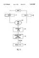
- FIG. 8shows a flow diagram of the second method.
- the first step 81is to add pegs of conductive thermoplastic adhesive to chip pad sites on the wafer. Then, in step 82, the insulative layer of adhesive is provided around the pegs.
- FIG. 9is a cross-sectional view of the final product, whether produced by the first or second methods.
- the conductive adhesive 4is surrounded by the insulative adhesive 2, and the composite adhesive structure 5 covers the entire surface of the substrate.
- the conductive adhesivemay project up above the level of the surrounding insulative adhesive and the holes may have a larger diameter than the bumps or pegs of conductive adhesive, but the volume of the conductive adhesive should be about the same as the holes, so that upon attachment, the two adhesives completely fill the space between the chip and substrate.
- FIG. 10illustrates a wafer 1, with a composite thermoplastic layer 5 ready to be sawn or diced into chips 6.
- the thickness of the thermoplastic adhesivesmust be sufficient to compensate for any bowing of the substrates (such as an FR-4 circuit board), and metal pad height tolerances, and to form a good void free bond.
- the thicknessis 1-5 mils for ceramic and flexible substrates and 3-8 mil to attach chips to organic substrates, such as FR-4.
- chips in the waferare formed with an electrically conductive adhesive in a two pass screen process to apply adhesive to the pad side of the wafer.
- the order of the stepsis not controlling.
- the first passapplies either the insulative or conductive adhesive to the chip bond pads.
- the second screeningwould apply the same or similar adhesive paste with a conductive or insulative filler to the same substrate surface.
- the addition of insulative filler to the insulative adhesiveis optional depending on coefficient of thermal expansion (CTE) requirements.
- CTEcoefficient of thermal expansion
- the insulative thermoplastic adhesiveis a dry fully polymerized dielectric adhesive preferably selected from one of the following polymer systems and may be filled with dielectric solids preferably ceramic particles, quartz, or glass.
- Preferred dielectric polymer systemsinclude thermoplastic polymers, copolymers, or blends. Examples of polymers include, but are not limited to, nylons, polysulfones, polyesters, flexible and soluble polyimides and siloxanes. Copolymers include, but are not limited to, random, segmented or block copolymers made of ethylene and vinyl acetate (EVA), siloxane and aryl-ethers, polyurethanes composed of polyisocyanate and polyethers or polyester segments.
- EVAethylene and vinyl acetate
- Blendsmay be of two or more polymers/copolymers such as ethylene-acrylate copolymer with polyethylene, EVA and poly(vinyl chloride) (PVC), polyester and PVC.
- Conductive thermoplastic systemsare composed of fully polymerized thermoplastic systems such as the above and electrically conductive particles made of or coated by Au, Ag, Pd or their oxide free, noble alloys.
- the fully polymerized thermoplastic system and fillersare thinned with a solvent or mixed a liquid to form an emulsion. After application the material is heated at an elevated temperature to evaporate the solvant or liquid until dry (non-tacky).
- the adhesiveIn order to bond the chip to the substrate the adhesive must be heated significantly above the transition temperature until it becomes tacky.
- the insulating and conductive adhesive materialsare preferably selected to be compatible during attachment processing.
- the thermoplastic materialsmust be chemically compatible so they do not negatively affect each others properties and preferably so that they bond together tightly for strength. Also, preferably the properties of the thermoplastics are similar to provide about the same CTE to minimize stresses and provide overlapping preferred drying and bonding temperature ranges.
- FIG. 11is a flow diagram illustrating preparing a chip to be placed on a chip carrier, starting with a wafer.
- the wafercan be prepared by either method, here indicated as Method I and denoted by reference numeral 111, where insulative thermoplastic adhesive paste is added to the wafer, dried (unless added as a pre-punched dry film adhesive bonded directly to the wafer surface), and then conductive thermoplastic adhesive paste is added to holes made in the insulative adhesive, or Method II and denoted by reference numeral 112, where conductive pegs of adhesive paste are added to the wafer, dried, then the insulative thermoplastic paste is applied to fill gaps between the conductive thermoplastic pegs.
- the waferis diced into chips in step 113.
- the chipsare placed in a die in step 114, and the die is pressed against a chip carrier and heat is added in step 115.
- the dieis removed in step 116, the chip remains adhered to the chip carrier.
- An optional step in this processis to add conductive thermoplastic adhesive to the pads on the chip carrier and drying the optional adhesive before pressing the die and chips against the chip carrier.
- Alternative manufacturing methods not illustratedinclude, applying the insulative adhesive to the chip carrier and the conductive adhesive bumps to the chip. After fitting the matching pieces together, heat and pressure are applied as in other methods. Also, both the insulative and conductive adhesives may be applied to the chip carrier by Methods I and II, using heat and pressure to attach the chip to the prepared chip carrier. Furthermore, the insulative and conductive adhesives may be applied to the chip carrier and in addition, conductive adhesive may be applied to the metal contact pads on the chip.
- FIG. 12illustrates a die 10 which may be used to add chips to a chip carrier 12, illustrated in FIG. 13.
- Chip carrier 12will have conductive pads to match the bumps of conductive adhesive 4 in the chip 6 to be adhered to the chip carrier.
- the chips 6are placed in recesses 13 on the die.
- the die 10is then pressed against the chip carrier 12 and heat is added. When the die is removed, the chips remain adhered to the chip carrier.
- FIG. 14shows a single chip adhered to the printed chip carrier after assembly.
- a chip 14is adhered to a chip carrier 12 with a layer of insulative thermoplastic adhesive 2 filling gaps between conductive thermoplastic adhesive 4 bumps.
- the electrically insulating thermoplastic adhesivecompletely fills the volume between the chip and the chip attach site around the electrically conductive adhesive pegs which adhesively connect between confronting pairs of metal contact pads.
- thermoplastic adhesiveis reworkable.
- Reworkingis illustrated in the flow chart depicted in FIG. 15. Because this is a thermoplastic adhesive, reworking is relatively simple and inexpensive.
- a die to fit the single chipis placed over the chip in step 151.
- the dieis heated and then removed, taking the chip with it in step 152. Any remaining adhesive may require removal using known solvents depending on the adhesive system.
- a new chipis then placed in a single chip die, pressed against the board with heat, and adhered to the board, much the same as in the original assembly of the printed chip carrier.
- a step which may be optional depending on chip size and planarity of the carrier surfacewould be to screen dispense electrically conductive adhesive onto the carrier pads as well and to dry this adhesive prior to connection (heat bonding).
- thermoplastic adhesiveIn preparation for bonding chips to a chip carrier or circuit board, individual chips are heated to a temperature significantly above the transition temperature at which the thermoplastic adhesive is in a soft, tacky state.
- the surface of the carrier chip siteis heated similarly.
- a typical temperaturewould be 150° to 300° C.
- An automatic chip placement toolwould be used to pick the chip and place the chip on the chip site of the carrier. Placement and bonding is accomplished in one step. Bonding occurs with time at temperature and pressure.
- the placement toolcan be set to apply the required bonding load (e.g.>30 psi) for the necessary time (e.g. several seconds).
- the electrical pads of the chip and carrierare interconnected with the electrically conductive adhesive.
- the insulative thermoplastic adhesivemechanically joins the chip to the carrier surface.
Landscapes
- Engineering & Computer Science (AREA)
- Computer Hardware Design (AREA)
- Microelectronics & Electronic Packaging (AREA)
- Power Engineering (AREA)
- Manufacturing & Machinery (AREA)
- Physics & Mathematics (AREA)
- Condensed Matter Physics & Semiconductors (AREA)
- General Physics & Mathematics (AREA)
- Wire Bonding (AREA)
- Connections Effected By Soldering, Adhesion, Or Permanent Deformation (AREA)
Abstract
Description
Claims (21)
Priority Applications (3)
| Application Number | Priority Date | Filing Date | Title |
|---|---|---|---|
| US08/190,507US5543585A (en) | 1994-02-02 | 1994-02-02 | Direct chip attachment (DCA) with electrically conductive adhesives |
| JP6324501AJP2596721B2 (en) | 1994-02-02 | 1994-12-27 | Method of manufacturing integrated circuit chip for DCA |
| US08/630,033US5747101A (en) | 1994-02-02 | 1996-04-09 | Direct chip attachment (DCA) with electrically conductive adhesives |
Applications Claiming Priority (1)
| Application Number | Priority Date | Filing Date | Title |
|---|---|---|---|
| US08/190,507US5543585A (en) | 1994-02-02 | 1994-02-02 | Direct chip attachment (DCA) with electrically conductive adhesives |
Related Child Applications (1)
| Application Number | Title | Priority Date | Filing Date |
|---|---|---|---|
| US08/630,033ContinuationUS5747101A (en) | 1994-02-02 | 1996-04-09 | Direct chip attachment (DCA) with electrically conductive adhesives |
Publications (1)
| Publication Number | Publication Date |
|---|---|
| US5543585Atrue US5543585A (en) | 1996-08-06 |
Family
ID=22701630
Family Applications (2)
| Application Number | Title | Priority Date | Filing Date |
|---|---|---|---|
| US08/190,507Expired - LifetimeUS5543585A (en) | 1994-02-02 | 1994-02-02 | Direct chip attachment (DCA) with electrically conductive adhesives |
| US08/630,033Expired - Fee RelatedUS5747101A (en) | 1994-02-02 | 1996-04-09 | Direct chip attachment (DCA) with electrically conductive adhesives |
Family Applications After (1)
| Application Number | Title | Priority Date | Filing Date |
|---|---|---|---|
| US08/630,033Expired - Fee RelatedUS5747101A (en) | 1994-02-02 | 1996-04-09 | Direct chip attachment (DCA) with electrically conductive adhesives |
Country Status (2)
| Country | Link |
|---|---|
| US (2) | US5543585A (en) |
| JP (1) | JP2596721B2 (en) |
Cited By (59)
| Publication number | Priority date | Publication date | Assignee | Title |
|---|---|---|---|---|
| US5611884A (en)* | 1995-12-11 | 1997-03-18 | Dow Corning Corporation | Flip chip silicone pressure sensitive conductive adhesive |
| US5759737A (en)* | 1996-09-06 | 1998-06-02 | International Business Machines Corporation | Method of making a component carrier |
| US5854514A (en)* | 1996-08-05 | 1998-12-29 | International Buisness Machines Corporation | Lead-free interconnection for electronic devices |
| US5879761A (en)* | 1989-12-18 | 1999-03-09 | Polymer Flip Chip Corporation | Method for forming electrically conductive polymer interconnects on electrical substrates |
| US5887343A (en)* | 1997-05-16 | 1999-03-30 | Harris Corporation | Direct chip attachment method |
| WO1999030362A1 (en)* | 1997-12-08 | 1999-06-17 | Minnesota Mining And Manufacturing Company | Method and apparatuses for making z-axis electrical connections |
| EP0907205A3 (en)* | 1997-10-02 | 1999-08-18 | Matsushita Electric Industrial Co., Ltd. | Semiconductor package and method for manufacturing the same |
| US5948922A (en)* | 1997-02-20 | 1999-09-07 | Cornell Research Foundation, Inc. | Compounds with substituted cyclic hydrocarbon moieties linked by secondary or tertiary oxycarbonyl containing moiety providing reworkable cured thermosets |
| WO1999056312A1 (en)* | 1998-04-27 | 1999-11-04 | Alpha Metals, Inc. | Flip chip with integrated flux, mask and underfill |
| US6100597A (en)* | 1996-11-15 | 2000-08-08 | Nec Corporation | Semiconductor device and method for manufacturing the same |
| EP0851724A3 (en)* | 1996-12-26 | 2000-09-27 | Matsushita Electric Industrial Co., Ltd. | Printed circuit board and electric components |
| EP1025587A4 (en)* | 1997-07-21 | 2000-10-04 | Aguila Technologies Inc | Semiconductor flip-chip package and method for the fabrication thereof |
| US6168972B1 (en) | 1998-12-22 | 2001-01-02 | Fujitsu Limited | Flip chip pre-assembly underfill process |
| US6189208B1 (en)* | 1998-09-11 | 2001-02-20 | Polymer Flip Chip Corp. | Flip chip mounting technique |
| US6218629B1 (en)* | 1999-01-20 | 2001-04-17 | International Business Machines Corporation | Module with metal-ion matrix induced dendrites for interconnection |
| US6219911B1 (en) | 1998-03-23 | 2001-04-24 | Polymer Flip Chip Corp. | Flip chip mounting technique |
| FR2803435A1 (en)* | 1999-12-30 | 2001-07-06 | Schlumberger Systems & Service | Method for flip-chip mounting of integrated circuits on electrical connection circuits, for use in production of contactless chip cards |
| US6268739B1 (en) | 1998-03-30 | 2001-07-31 | International Business Machines Corporation | Method and device for semiconductor testing using electrically conductive adhesives |
| US20010018800A1 (en)* | 1999-09-17 | 2001-09-06 | George Tzanavaras | Method for forming interconnects |
| US6296173B2 (en)* | 1996-07-17 | 2001-10-02 | International Business Machines Corporation | Method and apparatus for soldering ball grid array modules to substrates |
| US6323062B1 (en) | 1998-04-27 | 2001-11-27 | Alpha Metals, Inc. | Wafer coating method for flip chips |
| US20020076948A1 (en)* | 2000-10-16 | 2002-06-20 | Brian Farrell | Method of manufacturing a fabric article to include electronic circuitry and an electrically active textile article |
| US6410415B1 (en) | 1999-03-23 | 2002-06-25 | Polymer Flip Chip Corporation | Flip chip mounting technique |
| US20020155661A1 (en)* | 1999-10-28 | 2002-10-24 | Massingill Thomas J. | Multi-chip module and method for forming and method for deplating defective capacitors |
| US6475555B2 (en) | 1999-10-29 | 2002-11-05 | International Business Machines Corporation | Process for screening features on an electronic substrate with a low viscosity paste |
| US20020187591A1 (en)* | 2001-06-07 | 2002-12-12 | United Test Center, Inc. | Packaging process for semiconductor package |
| US20030035272A1 (en)* | 2001-05-29 | 2003-02-20 | Curcio Brian E. | Solid via layer to layer interconnect |
| US6535237B1 (en)* | 1996-08-09 | 2003-03-18 | Hewlett-Packard Company | Manufacture of fluid ejection device |
| EP1022774A3 (en)* | 1999-01-21 | 2003-08-06 | Lucent Technologies Inc. | Flip chip assembly of semiconductor IC chips |
| US6615484B2 (en)* | 1997-09-05 | 2003-09-09 | Litton Systems, Inc. | Method of manufacturing an electrical connection using solder flux compatible with flip chip underfill material |
| US6651319B2 (en) | 2001-09-07 | 2003-11-25 | Visteon Global Technologies, Inc. | Compliant standoff for low pressure sensing device |
| US6680436B2 (en) | 2000-07-12 | 2004-01-20 | Seagate Technology Llc | Reflow encapsulant |
| FR2842943A1 (en)* | 2002-07-24 | 2004-01-30 | Commissariat Energie Atomique | METHOD FOR MANUFACTURING ANISOTROPIC CONDUCTIVE POLYMER FILM ON SEMICONDUCTOR WAFER |
| US20040074952A1 (en)* | 2002-10-16 | 2004-04-22 | Stipp John N. | Method of controlling solder deposition utilizing two fluxes and preform |
| US6727197B1 (en) | 1999-11-18 | 2004-04-27 | Foster-Miller, Inc. | Wearable transmission device |
| US6734368B1 (en)* | 1997-07-09 | 2004-05-11 | International Business Machines Corporation | Metal backed printed circuit board assemblies |
| US20040092186A1 (en)* | 2000-11-17 | 2004-05-13 | Patricia Wilson-Nguyen | Textile electronic connection system |
| US20040251561A1 (en)* | 2003-06-11 | 2004-12-16 | Fry's Metals, Inc. | Thermoplastic fluxing underfill composition and method |
| US20050040514A1 (en)* | 2003-08-22 | 2005-02-24 | Samsung Electronics Co., Ltd. | Semiconductor package with improved chip attachment and manufacturing method thereof |
| US20050212105A1 (en)* | 2004-03-23 | 2005-09-29 | Walk Michael J | Integrated circuit die and substrate coupling |
| US20060030682A1 (en)* | 2004-08-05 | 2006-02-09 | Frys Metals, Inc. | Low voiding no flow fluxing underfill for electronic devices |
| US20060134387A1 (en)* | 2004-12-20 | 2006-06-22 | William Gottermeier | Multilayer article formed by adhesive ablation |
| US20070051774A1 (en)* | 2005-09-06 | 2007-03-08 | Stipp John N | Method of controlling solder deposition on heat spreader used for semiconductor package |
| US20070102827A1 (en)* | 1997-12-08 | 2007-05-10 | 3M Innovative Properties Company | Solvent Assisted Burnishing of Pre-Underfilled Solder-Bumped Wafers for Flipchip Bonding |
| US20070284135A1 (en)* | 2006-06-12 | 2007-12-13 | Fujitsu Limited | Flexible printed-circuit boards bonding method and printed circuit board |
| US20080011289A1 (en)* | 2006-07-14 | 2008-01-17 | National Science And Technology Development Agency | Photovoltaic thermal (PVT) collector |
| US7559902B2 (en) | 2003-08-22 | 2009-07-14 | Foster-Miller, Inc. | Physiological monitoring garment |
| US20100061056A1 (en)* | 2008-09-08 | 2010-03-11 | Damion Searls | Mainboard assembly including a package overlying a die directly attached to the mainboard |
| US8585606B2 (en) | 2010-09-23 | 2013-11-19 | QinetiQ North America, Inc. | Physiological status monitoring system |
| US9028404B2 (en) | 2010-07-28 | 2015-05-12 | Foster-Miller, Inc. | Physiological status monitoring system |
| USD729808S1 (en) | 2013-03-13 | 2015-05-19 | Nagrastar Llc | Smart card interface |
| US9211085B2 (en) | 2010-05-03 | 2015-12-15 | Foster-Miller, Inc. | Respiration sensing system |
| USD758372S1 (en)* | 2013-03-13 | 2016-06-07 | Nagrastar Llc | Smart card interface |
| USD759022S1 (en)* | 2013-03-13 | 2016-06-14 | Nagrastar Llc | Smart card interface |
| USD780763S1 (en) | 2015-03-20 | 2017-03-07 | Nagrastar Llc | Smart card interface |
| US9647997B2 (en) | 2013-03-13 | 2017-05-09 | Nagrastar, Llc | USB interface for performing transport I/O |
| US9769521B2 (en) | 2013-03-13 | 2017-09-19 | Nagrastar, Llc | Systems and methods for performing transport I/O |
| USD864968S1 (en) | 2015-04-30 | 2019-10-29 | Echostar Technologies L.L.C. | Smart card interface |
| CN116504646A (en)* | 2023-06-21 | 2023-07-28 | 青岛泰睿思微电子有限公司 | Multi-chip arrangement packaging structure and method |
Families Citing this family (26)
| Publication number | Priority date | Publication date | Assignee | Title |
|---|---|---|---|---|
| JPH0964244A (en)* | 1995-08-17 | 1997-03-07 | Hitachi Ltd | Semiconductor device and manufacturing method thereof |
| JP2751912B2 (en)* | 1996-03-28 | 1998-05-18 | 日本電気株式会社 | Semiconductor device and manufacturing method thereof |
| US6635514B1 (en)* | 1996-12-12 | 2003-10-21 | Tessera, Inc. | Compliant package with conductive elastomeric posts |
| JP3417292B2 (en)* | 1998-04-08 | 2003-06-16 | 松下電器産業株式会社 | Semiconductor device |
| US6008070A (en)* | 1998-05-21 | 1999-12-28 | Micron Technology, Inc. | Wafer level fabrication and assembly of chip scale packages |
| US6114181A (en)* | 1998-08-05 | 2000-09-05 | International Business Machines Corporation | Pre burn-in thermal bump card attach simulation to enhance reliability |
| JP2000114204A (en) | 1998-10-01 | 2000-04-21 | Mitsubishi Electric Corp | Wafer sheet, method of manufacturing semiconductor device using the same, and semiconductor manufacturing apparatus |
| US6350664B1 (en)* | 1999-09-02 | 2002-02-26 | Matsushita Electric Industrial Co., Ltd. | Semiconductor device and method of manufacturing the same |
| US6388335B1 (en)* | 1999-12-14 | 2002-05-14 | Atmel Corporation | Integrated circuit package formed at a wafer level |
| US6710454B1 (en)* | 2000-02-16 | 2004-03-23 | Micron Technology, Inc. | Adhesive layer for an electronic apparatus having multiple semiconductor devices |
| US6909180B2 (en)* | 2000-05-12 | 2005-06-21 | Matsushita Electric Industrial Co., Ltd. | Semiconductor device, mounting circuit board, method of producing the same, and method of producing mounting structure using the same |
| US6333104B1 (en)* | 2000-05-30 | 2001-12-25 | International Business Machines Corporation | Conductive polymer interconnection configurations |
| DE10059178C2 (en)* | 2000-11-29 | 2002-11-07 | Siemens Production & Logistics | Method for producing semiconductor modules and module produced using the method |
| US6872635B2 (en) | 2001-04-11 | 2005-03-29 | Sony Corporation | Device transferring method, and device arraying method and image display unit fabricating method using the same |
| FR2828334A1 (en)* | 2001-08-03 | 2003-02-07 | Schlumberger Systems & Service | Restoration of electrical and mechanical connectability to an electrical device with a face equipped with contact studs using an fixing layer crossed by conducting tracks |
| US6550666B2 (en)* | 2001-08-21 | 2003-04-22 | Advanpack Solutions Pte Ltd | Method for forming a flip chip on leadframe semiconductor package |
| CA2405368C (en)* | 2002-09-26 | 2011-06-21 | Crosslink Technology Inc. | Method of adhering a material to another material and product produced by the method |
| DE10342980B3 (en)* | 2003-09-17 | 2005-01-05 | Disco Hi-Tec Europe Gmbh | Semiconductor chip stack formation method for manufacture of 3D-packages with function testing of chips for removal or unacceptable chips and replacement by acceptable chips |
| US20070299325A1 (en)* | 2004-08-20 | 2007-12-27 | Brian Farrell | Physiological status monitoring system |
| JP2006128567A (en)* | 2004-11-01 | 2006-05-18 | Three M Innovative Properties Co | Method of connecting semiconductor package to printed wiring board |
| KR100601762B1 (en)* | 2004-11-09 | 2006-07-19 | 삼성전자주식회사 | Method for manufacturing flip chip bonding using non-conductive adhesive |
| JP2006184864A (en)* | 2004-12-03 | 2006-07-13 | Hitachi Cable Ltd | Polymer optical waveguide manufacturing method and polymer optical waveguide |
| TWI280618B (en)* | 2005-06-08 | 2007-05-01 | Advanced Semiconductor Eng | Method for machining a wafer |
| WO2007140448A2 (en)* | 2006-05-31 | 2007-12-06 | Teka Interconnection Systems | Solder-bearing articles and method of retaining a solder mass along a side edge thereof |
| US7829380B2 (en)* | 2006-10-31 | 2010-11-09 | Qimonda Ag | Solder pillar bumping and a method of making the same |
| US7973417B2 (en)* | 2008-04-18 | 2011-07-05 | Qimonda Ag | Integrated circuit and method of fabricating the same |
Citations (30)
| Publication number | Priority date | Publication date | Assignee | Title |
|---|---|---|---|---|
| US4012832A (en)* | 1976-03-12 | 1977-03-22 | Sperry Rand Corporation | Method for non-destructive removal of semiconductor devices |
| US4050756A (en)* | 1975-12-22 | 1977-09-27 | International Telephone And Telegraph Corporation | Conductive elastomer connector and method of making same |
| US4067104A (en)* | 1977-02-24 | 1978-01-10 | Rockwell International Corporation | Method of fabricating an array of flexible metallic interconnects for coupling microelectronics components |
| US4113981A (en)* | 1974-08-14 | 1978-09-12 | Kabushiki Kaisha Seikosha | Electrically conductive adhesive connecting arrays of conductors |
| US4157932A (en)* | 1976-11-04 | 1979-06-12 | Canon Kabushiki Kaisha | Connecting method |
| US4423435A (en)* | 1980-10-27 | 1983-12-27 | Texas Instruments Incorporated | Assembly of an electronic device on an insulative substrate |
| US4437109A (en)* | 1980-11-07 | 1984-03-13 | General Electric Company | Silicon-on-sapphire body with conductive paths therethrough |
| US4603374A (en)* | 1984-07-03 | 1986-07-29 | Motorola, Inc. | Packaging module for a semiconductor wafer |
| US4661192A (en)* | 1985-08-22 | 1987-04-28 | Motorola, Inc. | Low cost integrated circuit bonding process |
| US4667401A (en)* | 1985-11-26 | 1987-05-26 | Clements James R | Method of making an electronic device using an uniaxial conductive adhesive |
| US4694572A (en)* | 1986-06-13 | 1987-09-22 | Tektronix, Inc. | Printed polymer circuit board method |
| US4720740A (en)* | 1985-11-26 | 1988-01-19 | Clements James R | Electronic device including uniaxial conductive adhesive and method of making same |
| US4779338A (en)* | 1986-01-22 | 1988-10-25 | Sharp Kabushiki Kaisha | Method of mounting LSI |
| US4811081A (en)* | 1987-03-23 | 1989-03-07 | Motorola, Inc. | Semiconductor die bonding with conductive adhesive |
| US4889980A (en)* | 1985-07-10 | 1989-12-26 | Casio Computer Co., Ltd. | Electronic memory card and method of manufacturing same |
| US4914057A (en)* | 1987-07-16 | 1990-04-03 | Sgs-Thomson Microelectronics S.A. | Contacting method and structure for integrated circuit pads |
| US4984358A (en)* | 1989-03-10 | 1991-01-15 | Microelectronics And Computer Technology Corporation | Method of assembling stacks of integrated circuit dies |
| US5001302A (en)* | 1988-12-29 | 1991-03-19 | Casio Computer Co., Ltd. | Connecting structure for an electronic part |
| US5038251A (en)* | 1987-04-08 | 1991-08-06 | Casio Computer Co., Ltd. | Electronic apparatus and a method for manufacturing the same |
| US5061657A (en)* | 1990-07-18 | 1991-10-29 | The United States Of America As Represented By The Secretary Of The Navy | Method of making integrated circuit to package electrical connections after encapsulation with an organic polymer |
| US5068714A (en)* | 1989-04-05 | 1991-11-26 | Robert Bosch Gmbh | Method of electrically and mechanically connecting a semiconductor to a substrate using an electrically conductive tacky adhesive and the device so made |
| US5072874A (en)* | 1991-01-31 | 1991-12-17 | Microelectronics And Computer Technology Corporation | Method and apparatus for using desoldering material |
| US5074947A (en)* | 1989-12-18 | 1991-12-24 | Epoxy Technology, Inc. | Flip chip technology using electrically conductive polymers and dielectrics |
| US5086558A (en)* | 1990-09-13 | 1992-02-11 | International Business Machines Corporation | Direct attachment of semiconductor chips to a substrate with a substrate with a thermoplastic interposer |
| JPH04113643A (en)* | 1990-09-03 | 1992-04-15 | Seiko Epson Corp | Semiconductor device |
| US5120678A (en)* | 1990-11-05 | 1992-06-09 | Motorola Inc. | Electrical component package comprising polymer-reinforced solder bump interconnection |
| US5147084A (en)* | 1990-07-18 | 1992-09-15 | International Business Machines Corporation | Interconnection structure and test method |
| US5192835A (en)* | 1990-10-09 | 1993-03-09 | Eastman Kodak Company | Bonding of solid state device to terminal board |
| US5255431A (en)* | 1992-06-26 | 1993-10-26 | General Electric Company | Method of using frozen epoxy for placing pin-mounted components in a circuit module |
| US5436412A (en)* | 1992-10-30 | 1995-07-25 | International Business Machines Corporation | Interconnect structure having improved metallization |
Family Cites Families (9)
| Publication number | Priority date | Publication date | Assignee | Title |
|---|---|---|---|---|
| DE3343362A1 (en)* | 1983-11-30 | 1985-06-05 | Siemens AG, 1000 Berlin und 8000 München | METHOD FOR GALVANIC PRODUCTION OF METALLIC, HECKER-LIKE CONNECTION CONTACTS |
| US4604644A (en)* | 1985-01-28 | 1986-08-05 | International Business Machines Corporation | Solder interconnection structure for joining semiconductor devices to substrates that have improved fatigue life, and process for making |
| JP2574369B2 (en)* | 1988-03-07 | 1997-01-22 | 松下電器産業株式会社 | Semiconductor chip mounted body and mounting method thereof |
| JPH0797602B2 (en)* | 1988-05-06 | 1995-10-18 | 日本電気株式会社 | Semiconductor integrated circuit device |
| JP2698462B2 (en)* | 1990-01-12 | 1998-01-19 | 松下電器産業株式会社 | Method for manufacturing semiconductor device |
| JPH0442550A (en)* | 1990-06-08 | 1992-02-13 | Matsushita Electric Ind Co Ltd | Method of mounting electronic component |
| US5550408A (en)* | 1992-11-18 | 1996-08-27 | Matsushita Electronics Corporation | Semiconductor device |
| KR100245257B1 (en)* | 1993-01-13 | 2000-02-15 | 윤종용 | Manufacturing method of semiconductor package at wafer level |
| US5583747A (en)* | 1993-11-01 | 1996-12-10 | Baird; John H. | Thermoplastic interconnect for electronic device and method for making |
- 1994
- 1994-02-02USUS08/190,507patent/US5543585A/ennot_activeExpired - Lifetime
- 1994-12-27JPJP6324501Apatent/JP2596721B2/ennot_activeExpired - Fee Related
- 1996
- 1996-04-09USUS08/630,033patent/US5747101A/ennot_activeExpired - Fee Related
Patent Citations (30)
| Publication number | Priority date | Publication date | Assignee | Title |
|---|---|---|---|---|
| US4113981A (en)* | 1974-08-14 | 1978-09-12 | Kabushiki Kaisha Seikosha | Electrically conductive adhesive connecting arrays of conductors |
| US4050756A (en)* | 1975-12-22 | 1977-09-27 | International Telephone And Telegraph Corporation | Conductive elastomer connector and method of making same |
| US4012832A (en)* | 1976-03-12 | 1977-03-22 | Sperry Rand Corporation | Method for non-destructive removal of semiconductor devices |
| US4157932A (en)* | 1976-11-04 | 1979-06-12 | Canon Kabushiki Kaisha | Connecting method |
| US4067104A (en)* | 1977-02-24 | 1978-01-10 | Rockwell International Corporation | Method of fabricating an array of flexible metallic interconnects for coupling microelectronics components |
| US4423435A (en)* | 1980-10-27 | 1983-12-27 | Texas Instruments Incorporated | Assembly of an electronic device on an insulative substrate |
| US4437109A (en)* | 1980-11-07 | 1984-03-13 | General Electric Company | Silicon-on-sapphire body with conductive paths therethrough |
| US4603374A (en)* | 1984-07-03 | 1986-07-29 | Motorola, Inc. | Packaging module for a semiconductor wafer |
| US4889980A (en)* | 1985-07-10 | 1989-12-26 | Casio Computer Co., Ltd. | Electronic memory card and method of manufacturing same |
| US4661192A (en)* | 1985-08-22 | 1987-04-28 | Motorola, Inc. | Low cost integrated circuit bonding process |
| US4720740A (en)* | 1985-11-26 | 1988-01-19 | Clements James R | Electronic device including uniaxial conductive adhesive and method of making same |
| US4667401A (en)* | 1985-11-26 | 1987-05-26 | Clements James R | Method of making an electronic device using an uniaxial conductive adhesive |
| US4779338A (en)* | 1986-01-22 | 1988-10-25 | Sharp Kabushiki Kaisha | Method of mounting LSI |
| US4694572A (en)* | 1986-06-13 | 1987-09-22 | Tektronix, Inc. | Printed polymer circuit board method |
| US4811081A (en)* | 1987-03-23 | 1989-03-07 | Motorola, Inc. | Semiconductor die bonding with conductive adhesive |
| US5038251A (en)* | 1987-04-08 | 1991-08-06 | Casio Computer Co., Ltd. | Electronic apparatus and a method for manufacturing the same |
| US4914057A (en)* | 1987-07-16 | 1990-04-03 | Sgs-Thomson Microelectronics S.A. | Contacting method and structure for integrated circuit pads |
| US5001302A (en)* | 1988-12-29 | 1991-03-19 | Casio Computer Co., Ltd. | Connecting structure for an electronic part |
| US4984358A (en)* | 1989-03-10 | 1991-01-15 | Microelectronics And Computer Technology Corporation | Method of assembling stacks of integrated circuit dies |
| US5068714A (en)* | 1989-04-05 | 1991-11-26 | Robert Bosch Gmbh | Method of electrically and mechanically connecting a semiconductor to a substrate using an electrically conductive tacky adhesive and the device so made |
| US5074947A (en)* | 1989-12-18 | 1991-12-24 | Epoxy Technology, Inc. | Flip chip technology using electrically conductive polymers and dielectrics |
| US5061657A (en)* | 1990-07-18 | 1991-10-29 | The United States Of America As Represented By The Secretary Of The Navy | Method of making integrated circuit to package electrical connections after encapsulation with an organic polymer |
| US5147084A (en)* | 1990-07-18 | 1992-09-15 | International Business Machines Corporation | Interconnection structure and test method |
| JPH04113643A (en)* | 1990-09-03 | 1992-04-15 | Seiko Epson Corp | Semiconductor device |
| US5086558A (en)* | 1990-09-13 | 1992-02-11 | International Business Machines Corporation | Direct attachment of semiconductor chips to a substrate with a substrate with a thermoplastic interposer |
| US5192835A (en)* | 1990-10-09 | 1993-03-09 | Eastman Kodak Company | Bonding of solid state device to terminal board |
| US5120678A (en)* | 1990-11-05 | 1992-06-09 | Motorola Inc. | Electrical component package comprising polymer-reinforced solder bump interconnection |
| US5072874A (en)* | 1991-01-31 | 1991-12-17 | Microelectronics And Computer Technology Corporation | Method and apparatus for using desoldering material |
| US5255431A (en)* | 1992-06-26 | 1993-10-26 | General Electric Company | Method of using frozen epoxy for placing pin-mounted components in a circuit module |
| US5436412A (en)* | 1992-10-30 | 1995-07-25 | International Business Machines Corporation | Interconnect structure having improved metallization |
Non-Patent Citations (4)
| Title |
|---|
| R. R. Bechard et al.; "Chip Salvage Head: Removes Good Chips From Bad Modules For Reuse"; IBM Tech. Disclosure Bulletin, vol. 26 No. 10A, Mar. 1984. |
| R. R. Bechard et al.; Chip Salvage Head: Removes Good Chips From Bad Modules For Reuse ; IBM Tech. Disclosure Bulletin, vol. 26 No. 10A, Mar. 1984.* |
| T. R. Anthony; "Forming Electrical Interconnections Through Semiconductor Wafers"; J. Appl. Phys. 52(8), Aug. 1981; pp. 5340-5349. |
| T. R. Anthony; Forming Electrical Interconnections Through Semiconductor Wafers ; J. Appl. Phys. 52(8), Aug. 1981; pp. 5340 5349.* |
Cited By (103)
| Publication number | Priority date | Publication date | Assignee | Title |
|---|---|---|---|---|
| US5879761A (en)* | 1989-12-18 | 1999-03-09 | Polymer Flip Chip Corporation | Method for forming electrically conductive polymer interconnects on electrical substrates |
| US6138348A (en)* | 1989-12-18 | 2000-10-31 | Polymer Flip Chip Corporation | Method of forming electrically conductive polymer interconnects on electrical substrates |
| US5611884A (en)* | 1995-12-11 | 1997-03-18 | Dow Corning Corporation | Flip chip silicone pressure sensitive conductive adhesive |
| US6192581B1 (en) | 1996-04-30 | 2001-02-27 | Matsushita Electric Industrial Co., Ltd. | Method of making printed circuit board |
| US6296173B2 (en)* | 1996-07-17 | 2001-10-02 | International Business Machines Corporation | Method and apparatus for soldering ball grid array modules to substrates |
| US5854514A (en)* | 1996-08-05 | 1998-12-29 | International Buisness Machines Corporation | Lead-free interconnection for electronic devices |
| US6535237B1 (en)* | 1996-08-09 | 2003-03-18 | Hewlett-Packard Company | Manufacture of fluid ejection device |
| US5759737A (en)* | 1996-09-06 | 1998-06-02 | International Business Machines Corporation | Method of making a component carrier |
| US6326234B1 (en) | 1996-11-15 | 2001-12-04 | Nec Corporation | Semiconductor device and method for manufacturing the same |
| US6100597A (en)* | 1996-11-15 | 2000-08-08 | Nec Corporation | Semiconductor device and method for manufacturing the same |
| US6281448B1 (en) | 1996-12-26 | 2001-08-28 | Matsushita Electric Industrial Co., Ltd. | Printed circuit board and electronic components |
| EP0851724A3 (en)* | 1996-12-26 | 2000-09-27 | Matsushita Electric Industrial Co., Ltd. | Printed circuit board and electric components |
| US5948922A (en)* | 1997-02-20 | 1999-09-07 | Cornell Research Foundation, Inc. | Compounds with substituted cyclic hydrocarbon moieties linked by secondary or tertiary oxycarbonyl containing moiety providing reworkable cured thermosets |
| US5973033A (en)* | 1997-02-20 | 1999-10-26 | Cornell Research Foundation, Inc. | Compounds with substituted cyclic hydrocarbon moieties linked by secondary or tertiary oxycarbonyl containing moiety providing reworkable cured thermosets |
| US5887343A (en)* | 1997-05-16 | 1999-03-30 | Harris Corporation | Direct chip attachment method |
| US6734368B1 (en)* | 1997-07-09 | 2004-05-11 | International Business Machines Corporation | Metal backed printed circuit board assemblies |
| EP1025587A4 (en)* | 1997-07-21 | 2000-10-04 | Aguila Technologies Inc | Semiconductor flip-chip package and method for the fabrication thereof |
| US6615484B2 (en)* | 1997-09-05 | 2003-09-09 | Litton Systems, Inc. | Method of manufacturing an electrical connection using solder flux compatible with flip chip underfill material |
| US6486006B2 (en) | 1997-10-02 | 2002-11-26 | Matsushita Electric Industrial Co., Ltd. | Semiconductor chip bonded to a thermal conductive sheet having a filled through hole for electrical connection |
| EP0907205A3 (en)* | 1997-10-02 | 1999-08-18 | Matsushita Electric Industrial Co., Ltd. | Semiconductor package and method for manufacturing the same |
| EP1174920A3 (en)* | 1997-10-02 | 2002-06-05 | Matsushita Electric Industrial Co., Ltd. | Semiconductor package |
| US6300686B1 (en) | 1997-10-02 | 2001-10-09 | Matsushita Electric Industrial Co., Ltd. | Semiconductor chip bonded to a thermal conductive sheet having a filled through hole for electrical connection |
| US20070102827A1 (en)* | 1997-12-08 | 2007-05-10 | 3M Innovative Properties Company | Solvent Assisted Burnishing of Pre-Underfilled Solder-Bumped Wafers for Flipchip Bonding |
| US6260264B1 (en) | 1997-12-08 | 2001-07-17 | 3M Innovative Properties Company | Methods for making z-axis electrical connections |
| KR100559914B1 (en)* | 1997-12-08 | 2006-03-13 | 미네소타 마이닝 앤드 매뉴팩춰링 캄파니 | Method and apparatus for forming a coaxial electrical connection |
| US7170185B1 (en) | 1997-12-08 | 2007-01-30 | 3M Innovative Properties Company | Solvent assisted burnishing of pre-underfilled solder bumped wafers for flipchip bonding |
| WO1999030362A1 (en)* | 1997-12-08 | 1999-06-17 | Minnesota Mining And Manufacturing Company | Method and apparatuses for making z-axis electrical connections |
| US6219911B1 (en) | 1998-03-23 | 2001-04-24 | Polymer Flip Chip Corp. | Flip chip mounting technique |
| US6268739B1 (en) | 1998-03-30 | 2001-07-31 | International Business Machines Corporation | Method and device for semiconductor testing using electrically conductive adhesives |
| US6288559B1 (en) | 1998-03-30 | 2001-09-11 | International Business Machines Corporation | Semiconductor testing using electrically conductive adhesives |
| US6559666B2 (en) | 1998-03-30 | 2003-05-06 | International Business Machines Corporation | Method and device for semiconductor testing using electrically conductive adhesives |
| US6265776B1 (en)* | 1998-04-27 | 2001-07-24 | Fry's Metals, Inc. | Flip chip with integrated flux and underfill |
| WO1999056312A1 (en)* | 1998-04-27 | 1999-11-04 | Alpha Metals, Inc. | Flip chip with integrated flux, mask and underfill |
| US6323062B1 (en) | 1998-04-27 | 2001-11-27 | Alpha Metals, Inc. | Wafer coating method for flip chips |
| US6189208B1 (en)* | 1998-09-11 | 2001-02-20 | Polymer Flip Chip Corp. | Flip chip mounting technique |
| US6168972B1 (en) | 1998-12-22 | 2001-01-02 | Fujitsu Limited | Flip chip pre-assembly underfill process |
| US6218629B1 (en)* | 1999-01-20 | 2001-04-17 | International Business Machines Corporation | Module with metal-ion matrix induced dendrites for interconnection |
| US6584684B2 (en) | 1999-01-20 | 2003-07-01 | International Business Machines | Method for assembling a carrier and a semiconductor device |
| EP1022774A3 (en)* | 1999-01-21 | 2003-08-06 | Lucent Technologies Inc. | Flip chip assembly of semiconductor IC chips |
| US6410415B1 (en) | 1999-03-23 | 2002-06-25 | Polymer Flip Chip Corporation | Flip chip mounting technique |
| US20010018800A1 (en)* | 1999-09-17 | 2001-09-06 | George Tzanavaras | Method for forming interconnects |
| US6882045B2 (en) | 1999-10-28 | 2005-04-19 | Thomas J. Massingill | Multi-chip module and method for forming and method for deplating defective capacitors |
| US20020155661A1 (en)* | 1999-10-28 | 2002-10-24 | Massingill Thomas J. | Multi-chip module and method for forming and method for deplating defective capacitors |
| US6475555B2 (en) | 1999-10-29 | 2002-11-05 | International Business Machines Corporation | Process for screening features on an electronic substrate with a low viscosity paste |
| US6727197B1 (en) | 1999-11-18 | 2004-04-27 | Foster-Miller, Inc. | Wearable transmission device |
| FR2803435A1 (en)* | 1999-12-30 | 2001-07-06 | Schlumberger Systems & Service | Method for flip-chip mounting of integrated circuits on electrical connection circuits, for use in production of contactless chip cards |
| US6680436B2 (en) | 2000-07-12 | 2004-01-20 | Seagate Technology Llc | Reflow encapsulant |
| US20020076948A1 (en)* | 2000-10-16 | 2002-06-20 | Brian Farrell | Method of manufacturing a fabric article to include electronic circuitry and an electrically active textile article |
| US20040224138A1 (en)* | 2000-10-16 | 2004-11-11 | Brian Farrell | Electrically active textile article |
| US6729025B2 (en) | 2000-10-16 | 2004-05-04 | Foster-Miller, Inc. | Method of manufacturing a fabric article to include electronic circuitry and an electrically active textile article |
| US20040092186A1 (en)* | 2000-11-17 | 2004-05-13 | Patricia Wilson-Nguyen | Textile electronic connection system |
| US20030035272A1 (en)* | 2001-05-29 | 2003-02-20 | Curcio Brian E. | Solid via layer to layer interconnect |
| US7076869B2 (en)* | 2001-05-29 | 2006-07-18 | International Business Machines Corporation | Solid via layer to layer interconnect |
| US20020187591A1 (en)* | 2001-06-07 | 2002-12-12 | United Test Center, Inc. | Packaging process for semiconductor package |
| US6752022B2 (en) | 2001-09-07 | 2004-06-22 | Visteon Global Technologies, Inc. | Compliant standoff for low pressure sensing device |
| US20040045382A1 (en)* | 2001-09-07 | 2004-03-11 | Visteon Global Technologies, Inc. | Compliant standoff for low pressure sensing device |
| US6651319B2 (en) | 2001-09-07 | 2003-11-25 | Visteon Global Technologies, Inc. | Compliant standoff for low pressure sensing device |
| US7026239B2 (en) | 2002-07-24 | 2006-04-11 | Commissariat A L'energie Atomique | Method for making an anisotropic conductive polymer film on a semiconductor wafer |
| US20040241932A1 (en)* | 2002-07-24 | 2004-12-02 | Jean-Charles Souriau | Method of making an anisotropic conductive polymer film on a semiconductor wafer |
| FR2842943A1 (en)* | 2002-07-24 | 2004-01-30 | Commissariat Energie Atomique | METHOD FOR MANUFACTURING ANISOTROPIC CONDUCTIVE POLYMER FILM ON SEMICONDUCTOR WAFER |
| WO2004012226A3 (en)* | 2002-07-24 | 2004-04-08 | Commissariat Energie Atomique | Method for making an anisotropic conductive polymer film on a semiconductor wafer |
| US6786391B2 (en) | 2002-10-16 | 2004-09-07 | Kac Holdings, Inc. | Method of controlling solder deposition utilizing two fluxes and preform |
| US20040074952A1 (en)* | 2002-10-16 | 2004-04-22 | Stipp John N. | Method of controlling solder deposition utilizing two fluxes and preform |
| US20040251561A1 (en)* | 2003-06-11 | 2004-12-16 | Fry's Metals, Inc. | Thermoplastic fluxing underfill composition and method |
| US20080108178A1 (en)* | 2003-06-11 | 2008-05-08 | Fry's Metals, Inc. | Thermoplastic fluxing underfill method |
| US7166491B2 (en) | 2003-06-11 | 2007-01-23 | Fry's Metals, Inc. | Thermoplastic fluxing underfill composition and method |
| US20080110530A1 (en)* | 2003-06-11 | 2008-05-15 | Fry's Metals, Inc. | Thermoplastic fluxing underfill composition |
| US20050040514A1 (en)* | 2003-08-22 | 2005-02-24 | Samsung Electronics Co., Ltd. | Semiconductor package with improved chip attachment and manufacturing method thereof |
| US7559902B2 (en) | 2003-08-22 | 2009-07-14 | Foster-Miller, Inc. | Physiological monitoring garment |
| US7235887B2 (en)* | 2003-08-22 | 2007-06-26 | Samsung Electronics Co., Ltd. | Semiconductor package with improved chip attachment and manufacturing method thereof |
| US20050212105A1 (en)* | 2004-03-23 | 2005-09-29 | Walk Michael J | Integrated circuit die and substrate coupling |
| WO2005101479A1 (en)* | 2004-03-23 | 2005-10-27 | Intel Corporation (A Delaware Corporation) | Integrated circuit die and substrate coupling |
| US7247683B2 (en) | 2004-08-05 | 2007-07-24 | Fry's Metals, Inc. | Low voiding no flow fluxing underfill for electronic devices |
| US20060030682A1 (en)* | 2004-08-05 | 2006-02-09 | Frys Metals, Inc. | Low voiding no flow fluxing underfill for electronic devices |
| US20060134387A1 (en)* | 2004-12-20 | 2006-06-22 | William Gottermeier | Multilayer article formed by adhesive ablation |
| US20070051774A1 (en)* | 2005-09-06 | 2007-03-08 | Stipp John N | Method of controlling solder deposition on heat spreader used for semiconductor package |
| US20070284135A1 (en)* | 2006-06-12 | 2007-12-13 | Fujitsu Limited | Flexible printed-circuit boards bonding method and printed circuit board |
| US7958632B2 (en)* | 2006-06-12 | 2011-06-14 | Fujitsu Limited | Flexible printed-circuit boards bonding method and printed circuit board |
| US20080011289A1 (en)* | 2006-07-14 | 2008-01-17 | National Science And Technology Development Agency | Photovoltaic thermal (PVT) collector |
| US20100061056A1 (en)* | 2008-09-08 | 2010-03-11 | Damion Searls | Mainboard assembly including a package overlying a die directly attached to the mainboard |
| US10555417B2 (en) | 2008-09-08 | 2020-02-04 | Intel Corporation | Mainboard assembly including a package overlying a die directly attached to the mainboard |
| US10251273B2 (en) | 2008-09-08 | 2019-04-02 | Intel Corporation | Mainboard assembly including a package overlying a die directly attached to the mainboard |
| US9211085B2 (en) | 2010-05-03 | 2015-12-15 | Foster-Miller, Inc. | Respiration sensing system |
| US9028404B2 (en) | 2010-07-28 | 2015-05-12 | Foster-Miller, Inc. | Physiological status monitoring system |
| US8585606B2 (en) | 2010-09-23 | 2013-11-19 | QinetiQ North America, Inc. | Physiological status monitoring system |
| USD792411S1 (en) | 2013-03-13 | 2017-07-18 | Nagrastar Llc | Smart card interface |
| US10070176B2 (en) | 2013-03-13 | 2018-09-04 | Nagrastar, Llc | Systems and methods for performing transport I/O |
| USD949864S1 (en)* | 2013-03-13 | 2022-04-26 | Nagrastar Llc | Smart card interface |
| US9647997B2 (en) | 2013-03-13 | 2017-05-09 | Nagrastar, Llc | USB interface for performing transport I/O |
| USD759022S1 (en)* | 2013-03-13 | 2016-06-14 | Nagrastar Llc | Smart card interface |
| USD792410S1 (en) | 2013-03-13 | 2017-07-18 | Nagrastar Llc | Smart card interface |
| US9769521B2 (en) | 2013-03-13 | 2017-09-19 | Nagrastar, Llc | Systems and methods for performing transport I/O |
| US9774908B2 (en) | 2013-03-13 | 2017-09-26 | Nagrastar, Llc | Systems and methods for performing transport I/O |
| US9888283B2 (en) | 2013-03-13 | 2018-02-06 | Nagrastar Llc | Systems and methods for performing transport I/O |
| USD780184S1 (en) | 2013-03-13 | 2017-02-28 | Nagrastar Llc | Smart card interface |
| USD840404S1 (en) | 2013-03-13 | 2019-02-12 | Nagrastar, Llc | Smart card interface |
| USD758372S1 (en)* | 2013-03-13 | 2016-06-07 | Nagrastar Llc | Smart card interface |
| US10382816B2 (en) | 2013-03-13 | 2019-08-13 | Nagrastar, Llc | Systems and methods for performing transport I/O |
| USD729808S1 (en) | 2013-03-13 | 2015-05-19 | Nagrastar Llc | Smart card interface |
| USD780763S1 (en) | 2015-03-20 | 2017-03-07 | Nagrastar Llc | Smart card interface |
| USD864968S1 (en) | 2015-04-30 | 2019-10-29 | Echostar Technologies L.L.C. | Smart card interface |
| CN116504646A (en)* | 2023-06-21 | 2023-07-28 | 青岛泰睿思微电子有限公司 | Multi-chip arrangement packaging structure and method |
| CN116504646B (en)* | 2023-06-21 | 2023-12-15 | 青岛泰睿思微电子有限公司 | Multi-chip arrangement packaging structure and method |
Also Published As
| Publication number | Publication date |
|---|---|
| JP2596721B2 (en) | 1997-04-02 |
| US5747101A (en) | 1998-05-05 |
| JPH07231011A (en) | 1995-08-29 |
Similar Documents
| Publication | Publication Date | Title |
|---|---|---|
| US5543585A (en) | Direct chip attachment (DCA) with electrically conductive adhesives | |
| US5086558A (en) | Direct attachment of semiconductor chips to a substrate with a substrate with a thermoplastic interposer | |
| EP0810649B1 (en) | Method for coupling substrates and structure | |
| JP4809761B2 (en) | Method for attaching area array device to electric substrate and patterned underfill film | |
| US6189208B1 (en) | Flip chip mounting technique | |
| US6548909B2 (en) | Method of interconnecting electronic components using a plurality of conductive studs | |
| US5744758A (en) | Multilayer circuit board and process of production thereof | |
| EP0876689B1 (en) | Method of forming electrical interconnects using isotropic conductive adhesives and connections formed thereby | |
| US6410415B1 (en) | Flip chip mounting technique | |
| JP4703556B2 (en) | Method of attaching flip chip to electrical substrate, flip chip assembly and method of forming underfill coated wafer | |
| US5147210A (en) | Polymer film interconnect | |
| US6147311A (en) | Multi layer circuit board using anisotropic electroconductive adhesive layer and method for producing same | |
| US6329609B1 (en) | Method and structure to prevent distortion and expansion of organic spacer layer for thin film transfer-join technology | |
| EP0831525A2 (en) | Method for forming protruding electrode | |
| US6933221B1 (en) | Method for underfilling semiconductor components using no flow underfill | |
| WO2012061199A2 (en) | No flow underfill | |
| KR20010032804A (en) | Method and apparatuses for making z-axis electrical connections | |
| US6058021A (en) | Structure of mounting a semiconductor element onto a substrate | |
| CN1093680C (en) | Electrode modification using unzippable polymer paste | |
| WO1990007792A1 (en) | Method of making high density solder bumps and a substrate socket for high density solder bumps | |
| US20010025874A1 (en) | Method of forming solder bumps, method of mounting flip chips, and a mounting structure | |
| JP3506003B2 (en) | Anisotropic conductive adhesive | |
| Saraf | Direct chip attachment (DCA) with electrically conductive adhesives | |
| JP2001135662A (en) | Semiconductor element and semiconductor device manufacturing method | |
| JPH0888248A (en) | Face-down bonding method and connecting material using thereof |
Legal Events
| Date | Code | Title | Description |
|---|---|---|---|
| AS | Assignment | Owner name:INTERNATIONAL BUSINESS MACHINES CORPORATION, NEW Y Free format text:ASSIGNMENT OF ASSIGNORS INTEREST;ASSIGNORS:BOOTH, RICHARD B.;GAYNES, MICHAEL A.;MURCKO, ROBERT M.;AND OTHERS;REEL/FRAME:006963/0225;SIGNING DATES FROM 19940216 TO 19940314 | |
| FEPP | Fee payment procedure | Free format text:PAYOR NUMBER ASSIGNED (ORIGINAL EVENT CODE: ASPN); ENTITY STATUS OF PATENT OWNER: LARGE ENTITY | |
| STCF | Information on status: patent grant | Free format text:PATENTED CASE | |
| FPAY | Fee payment | Year of fee payment:4 | |
| FEPP | Fee payment procedure | Free format text:PAYOR NUMBER ASSIGNED (ORIGINAL EVENT CODE: ASPN); ENTITY STATUS OF PATENT OWNER: LARGE ENTITY Free format text:PAYER NUMBER DE-ASSIGNED (ORIGINAL EVENT CODE: RMPN); ENTITY STATUS OF PATENT OWNER: LARGE ENTITY | |
| FPAY | Fee payment | Year of fee payment:8 | |
| FPAY | Fee payment | Year of fee payment:12 | |
| AS | Assignment | Owner name:GLOBALFOUNDRIES U.S. 2 LLC, NEW YORK Free format text:ASSIGNMENT OF ASSIGNORS INTEREST;ASSIGNOR:INTERNATIONAL BUSINESS MACHINES CORPORATION;REEL/FRAME:036550/0001 Effective date:20150629 | |
| AS | Assignment | Owner name:GLOBALFOUNDRIES INC., CAYMAN ISLANDS Free format text:ASSIGNMENT OF ASSIGNORS INTEREST;ASSIGNORS:GLOBALFOUNDRIES U.S. 2 LLC;GLOBALFOUNDRIES U.S. INC.;REEL/FRAME:036779/0001 Effective date:20150910 |