US5539214A - Quantum bridges fabricated by selective etching of superlattice structures - Google Patents
Quantum bridges fabricated by selective etching of superlattice structuresDownload PDFInfo
- Publication number
- US5539214A US5539214AUS08/384,166US38416695AUS5539214AUS 5539214 AUS5539214 AUS 5539214AUS 38416695 AUS38416695 AUS 38416695AUS 5539214 AUS5539214 AUS 5539214A
- Authority
- US
- United States
- Prior art keywords
- quantum
- wires
- semiconductor material
- silicon
- bridge
- Prior art date
- Legal status (The legal status is an assumption and is not a legal conclusion. Google has not performed a legal analysis and makes no representation as to the accuracy of the status listed.)
- Expired - Fee Related
Links
- 238000005530etchingMethods0.000titleabstractdescription8
- 229910052710siliconInorganic materials0.000claimsabstractdescription38
- 239000010703siliconSubstances0.000claimsabstractdescription38
- 239000000463materialSubstances0.000claimsabstractdescription20
- 239000004065semiconductorSubstances0.000claimsabstractdescription20
- 229910052732germaniumInorganic materials0.000claimsdescription12
- GNPVGFCGXDBREM-UHFFFAOYSA-Ngermanium atomChemical compound[Ge]GNPVGFCGXDBREM-UHFFFAOYSA-N0.000claimsdescription12
- 239000000758substrateSubstances0.000claimsdescription11
- 239000002019doping agentSubstances0.000claimsdescription6
- 239000000126substanceSubstances0.000abstractdescription4
- 230000003247decreasing effectEffects0.000abstractdescription2
- XUIMIQQOPSSXEZ-UHFFFAOYSA-NSiliconChemical compound[Si]XUIMIQQOPSSXEZ-UHFFFAOYSA-N0.000description34
- 238000000034methodMethods0.000description4
- 238000005424photoluminescenceMethods0.000description3
- 229910021426porous siliconInorganic materials0.000description3
- 241000894007speciesSpecies0.000description3
- JBRZTFJDHDCESZ-UHFFFAOYSA-NAsGaChemical compound[As]#[Ga]JBRZTFJDHDCESZ-UHFFFAOYSA-N0.000description2
- KRHYYFGTRYWZRS-UHFFFAOYSA-NFluoraneChemical compoundFKRHYYFGTRYWZRS-UHFFFAOYSA-N0.000description2
- 229910001218Gallium arsenideInorganic materials0.000description2
- VYPSYNLAJGMNEJ-UHFFFAOYSA-NSilicium dioxideChemical compoundO=[Si]=OVYPSYNLAJGMNEJ-UHFFFAOYSA-N0.000description2
- 230000001419dependent effectEffects0.000description2
- 238000001514detection methodMethods0.000description2
- 238000005401electroluminescenceMethods0.000description2
- 238000005468ion implantationMethods0.000description2
- 238000004020luminiscence typeMethods0.000description2
- 238000004519manufacturing processMethods0.000description2
- 229910052751metalInorganic materials0.000description2
- 239000002184metalSubstances0.000description2
- 230000003287optical effectEffects0.000description2
- 238000000206photolithographyMethods0.000description2
- 150000003376siliconChemical class0.000description2
- 229910052814silicon oxideInorganic materials0.000description2
- XLYOFNOQVPJJNP-UHFFFAOYSA-NwaterSubstancesOXLYOFNOQVPJJNP-UHFFFAOYSA-N0.000description2
- 238000001039wet etchingMethods0.000description2
- 229910000980Aluminium gallium arsenideInorganic materials0.000description1
- XPDWGBQVDMORPB-UHFFFAOYSA-NFluoroformChemical compoundFC(F)FXPDWGBQVDMORPB-UHFFFAOYSA-N0.000description1
- 230000005355Hall effectEffects0.000description1
- 229910052581Si3N4Inorganic materials0.000description1
- LEVVHYCKPQWKOP-UHFFFAOYSA-N[Si].[Ge]Chemical compound[Si].[Ge]LEVVHYCKPQWKOP-UHFFFAOYSA-N0.000description1
- 238000010521absorption reactionMethods0.000description1
- FTWRSWRBSVXQPI-UHFFFAOYSA-Nalumanylidynearsane;gallanylidynearsaneChemical compound[As]#[Al].[As]#[Ga]FTWRSWRBSVXQPI-UHFFFAOYSA-N0.000description1
- 230000009286beneficial effectEffects0.000description1
- 239000000969carrierSubstances0.000description1
- 239000004020conductorSubstances0.000description1
- 238000010586diagramMethods0.000description1
- 238000009826distributionMethods0.000description1
- 230000000694effectsEffects0.000description1
- 150000002500ionsChemical class0.000description1
- 230000037230mobilityEffects0.000description1
- 238000012986modificationMethods0.000description1
- 230000004048modificationEffects0.000description1
- 238000001451molecular beam epitaxyMethods0.000description1
- 230000003534oscillatory effectEffects0.000description1
- 229920002120photoresistant polymerPolymers0.000description1
- 238000001020plasma etchingMethods0.000description1
- 238000004886process controlMethods0.000description1
- 238000010791quenchingMethods0.000description1
- 230000000171quenching effectEffects0.000description1
- HQVNEWCFYHHQES-UHFFFAOYSA-Nsilicon nitrideChemical compoundN12[Si]34N5[Si]62N3[Si]51N64HQVNEWCFYHHQES-UHFFFAOYSA-N0.000description1
- 238000001179sorption measurementMethods0.000description1
- 238000001228spectrumMethods0.000description1
- 238000004381surface treatmentMethods0.000description1
Images


Classifications
- H—ELECTRICITY
- H10—SEMICONDUCTOR DEVICES; ELECTRIC SOLID-STATE DEVICES NOT OTHERWISE PROVIDED FOR
- H10H—INORGANIC LIGHT-EMITTING SEMICONDUCTOR DEVICES HAVING POTENTIAL BARRIERS
- H10H20/00—Individual inorganic light-emitting semiconductor devices having potential barriers, e.g. light-emitting diodes [LED]
- H10H20/80—Constructional details
- H10H20/81—Bodies
- H10H20/811—Bodies having quantum effect structures or superlattices, e.g. tunnel junctions
- H10H20/812—Bodies having quantum effect structures or superlattices, e.g. tunnel junctions within the light-emitting regions, e.g. having quantum confinement structures
- B—PERFORMING OPERATIONS; TRANSPORTING
- B82—NANOTECHNOLOGY
- B82Y—SPECIFIC USES OR APPLICATIONS OF NANOSTRUCTURES; MEASUREMENT OR ANALYSIS OF NANOSTRUCTURES; MANUFACTURE OR TREATMENT OF NANOSTRUCTURES
- B82Y10/00—Nanotechnology for information processing, storage or transmission, e.g. quantum computing or single electron logic
- B—PERFORMING OPERATIONS; TRANSPORTING
- B82—NANOTECHNOLOGY
- B82Y—SPECIFIC USES OR APPLICATIONS OF NANOSTRUCTURES; MEASUREMENT OR ANALYSIS OF NANOSTRUCTURES; MANUFACTURE OR TREATMENT OF NANOSTRUCTURES
- B82Y20/00—Nanooptics, e.g. quantum optics or photonic crystals
- H—ELECTRICITY
- H10—SEMICONDUCTOR DEVICES; ELECTRIC SOLID-STATE DEVICES NOT OTHERWISE PROVIDED FOR
- H10D—INORGANIC ELECTRIC SEMICONDUCTOR DEVICES
- H10D62/00—Semiconductor bodies, or regions thereof, of devices having potential barriers
- H10D62/80—Semiconductor bodies, or regions thereof, of devices having potential barriers characterised by the materials
- H10D62/81—Semiconductor bodies, or regions thereof, of devices having potential barriers characterised by the materials of structures exhibiting quantum-confinement effects, e.g. single quantum wells; of structures having periodic or quasi-periodic potential variation
- H10D62/812—Single quantum well structures
- H10D62/813—Quantum wire structures
- H—ELECTRICITY
- H10—SEMICONDUCTOR DEVICES; ELECTRIC SOLID-STATE DEVICES NOT OTHERWISE PROVIDED FOR
- H10F—INORGANIC SEMICONDUCTOR DEVICES SENSITIVE TO INFRARED RADIATION, LIGHT, ELECTROMAGNETIC RADIATION OF SHORTER WAVELENGTH OR CORPUSCULAR RADIATION
- H10F77/00—Constructional details of devices covered by this subclass
- H10F77/10—Semiconductor bodies
- H10F77/14—Shape of semiconductor bodies; Shapes, relative sizes or dispositions of semiconductor regions within semiconductor bodies
- H10F77/146—Superlattices; Multiple quantum well structures
- H10F77/1465—Superlattices; Multiple quantum well structures including only Group IV materials, e.g. Si-SiGe superlattices
- H—ELECTRICITY
- H10—SEMICONDUCTOR DEVICES; ELECTRIC SOLID-STATE DEVICES NOT OTHERWISE PROVIDED FOR
- H10H—INORGANIC LIGHT-EMITTING SEMICONDUCTOR DEVICES HAVING POTENTIAL BARRIERS
- H10H20/00—Individual inorganic light-emitting semiconductor devices having potential barriers, e.g. light-emitting diodes [LED]
- H10H20/80—Constructional details
- H10H20/81—Bodies
- H10H20/811—Bodies having quantum effect structures or superlattices, e.g. tunnel junctions
Definitions
- This inventionrelates generally to bandgap engineered semiconductor structures and more particularly the invention relates to structures having dimensions sufficiently small so as to confine carriers located therein and resulting in novel electronic and optical properties.
- quantum wiresmay show significant improvements in transport properties over bulk semiconductors due to decreased Coulomb scattering.
- Many other novel effects related to the quantum confinementhave been reported such as non-local bend resistance, the quenching of the Hall effect, and the oscillatory behavior of capacitance and conductivity.
- the optical properties of porous siliconcan be combined with the improved electrical property to function as sensors.
- quantum wire superlattices in gallium arsenide/aluminum gallium arsenidehave been proposed for 8-20 micrometer photodetectors.
- a theoretical study of p-i-n GaAs/AlGaAs quantum wire detectorsproposes that they may perform better than bulk devices due to increased absorption of photons and the higher carrier mobilities therein. See D. L. Crawford et al., Applied Physics Letters, 58 (1991), p. 1629.
- the present inventionis directed to the fabrication of a quantum bridge structure whose length, width, and height can be controlled by processing parameters.
- the resulting structurecan exhibit photoluminescence and electroluminescence which allows the device to function in a light emitter, light detector, conductive wire, and a sensor mode.
- quantum bridgesare provided by the selective etching of superlattice structures.
- the physical dimensions as well as the photoluminescence and electroluminescence of the bridge structurecan be readily varied.
- the resulting structurecan then be employed in various applications of light emission, light detection, and electrical conduction.
- the process in fabricating the quantum bridge structurebegins with a supporting substrate of silicon or other material on which a silicon buffer layer can be epitaxially grown.
- a silicon buffer layercan be epitaxially grown.
- a graded silicon to Si x Ge 1-x buffer layeris then epitaxially grown on the silicon buffer layer.
- a superlattice structure of alternating silicon and germanium layersis then grown on the silicon/germanium buffer layer.
- the bridge structureis then formed by selectively etching trenches through the superlattice structure using E-beam or I-beam photolithography and plasma etching. Germanium material between the silicon wires is then removed by selective wet etching. Contacts at either end of the wire structure are formed by high energy ion implantation into supporting superlattice columns.
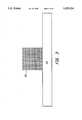
- FIG. 1is a top view of a quantum bridge structure in accordance with one embodiment of the invention.
- FIG. 2is a side view of the quantum bridge structure of FIG. 1.
- FIG. 3is a cross-section view of the quantum bridge structure of FIGS. 1 and 2 taken along the line 3--3 in FIG. 2.
- FIG. 4is a flow diagram of a process for fabricating the quantum bridge structure in accordance with the invention.
- FIGS. 1, 2, and 3are a top view, side view, and cross-section view of a quantum bridge structure in accordance with one embodiment of the invention.
- the structureis fabricated on a supporting substrate 10 of silicon, or a substrate on which a buffer layer of silicon can be grown.
- the bridge structureincludes a plurality of silicon wires 12 which are supported at either end by superlattice germanium-silicon columns 14. Electrical contacts to the quantum wires 12 are provided by implanted dopant ions in the superlattice supports 14 with suitable metal contacts 16 provided on the superlattice supports 14.
- the quantum bridgeis a mesa structure on the supporting substrate formed by removing by etching surrounding material.
- the quantum wires 12are fabricated by etching parallel trenches perpendicular to the plane of the superlattice layers and then removing by preferential etchant the alternating layers of germanium in the superlattice.
- the trenches down to the substrateare visible while the side view of FIG. 2 illustrates the superlattice layering of the structure with the wires in the middle portion of the structure formed by removing selectively etched germanium between the silicon wires. In the unetched areas the superlattice remains intact as grown to provide supports and low resistance paths to the silicon wires.
- FIG. 3shows a cross-section of the quantum wire structure taken along the line 3--3 of FIG. 2.
- the number of rows and columns of wirescan be varied as can be the cross-sectional shape and dimensions of the wires. While the wires are illustrated as uniformly spaced, the spacing between wires both vertically and horizontally is readily varied by process control.
- the vertical height of the wires, vertical spacing between wires, and number of rowsare varied by changing the thicknesses and numbers of layers epitaxially deposited.
- Horizontal width of the wires, horizontal spacing between wires, and the number of wiresare varied by changing the width, spacing, and the number of trenches. Further, all wires need not have the same dimensions. Varying dimensions within one structure can lead to possible additional beneficial effects, such as luminescence over a broader wave length spectrum.
- FIG. 4is a process flow in the fabrication of the quantum bridge structure in accordance with one embodiment of the invention.
- the superlattice layersare grown on a supporting substrate by using molecular beam epitaxy.
- the supporting substrateincludes a silicon substrate or a silicon buffer layer of 3,000 ⁇ on a supporting substrate.
- a 2.5 micron silicon to Si 0 .5 Ge 0 .5 graded bufferis formed on the silicon buffer layer.
- a 1.0 micron thick Si 0 .5 Ge 0 .5 bufferis then formed on the graded buffer.
- alternating layers of silicon and germaniumare epitaxially grown with each layer being on the order of 500 ⁇ in thickness.
- the alternating layerscan comprise the same material silicon, for example, with adjacent layers being distinguished by doping.
- a layer of undoped siliconcan be preferentially etched over doped silicon.
- EPWethylenediamine-pyrocatechol-water
- a cap layer of silicon oxide or silicon oxide/silicon nitrideis then formed on the top silicon layer as a hard mask, and a trench pattern is defined thereon using E-beam or I-beam photolithography in developing a photo resist.
- a tight pitch array of linescan thus be etched through the cap layer.
- slotsare etched through the underlying superlattice structure using a suitable dry etch which can include a number of etching species including CF 4 , CHF 3 , SF 6 and combinations thereof with O 2 .
- the alternate layers of germanium between the silicon layersare removed by selective wet etching which can consist of a combination of HF, H 2 O 2 , and H 2 O which etches germanium considerably faster than silicon.
- an etchantwith an etch rate that is dependent on doping will be employed.
- EPWethylenediamine-pyrocatechol-water
- the electrical contacts through the superlattice structures 14 at either end of the bridgeare formed by high energy ion implantation through the superlattice structure, preferably before the etching of the germanium layers.
- Metal bonding contacts 16are then provided on the top surfaces of the superlattice structures 14.
- the resulting bridge structurehas many applications as a light emitter, a light sensor, a chemical sensor, and electrical current conductor.
- a distribution of wave length emissionscan be controlled by adjusting pattern dimensions and by surface treatment. For example, luminescence increases with a passivating oxide and almost completely disappears after a dip in hydrofluoric acid to remove the oxide.
- the change in quantum properties, electrical and light emission and detection, due to chemical adsorptionmakes the bridge structure suitable for use as a chemical sensor.
- the precise control over small dimensions of the silicon wires in the bridge structurepermits a desired light emission or obstruction of species on a pretreated surface which permits the structure to function as a detector for that species.
Landscapes
- Engineering & Computer Science (AREA)
- Chemical & Material Sciences (AREA)
- Nanotechnology (AREA)
- Physics & Mathematics (AREA)
- Crystallography & Structural Chemistry (AREA)
- Life Sciences & Earth Sciences (AREA)
- Biophysics (AREA)
- Optics & Photonics (AREA)
- Mathematical Physics (AREA)
- Theoretical Computer Science (AREA)
- Led Devices (AREA)
- Light Receiving Elements (AREA)
Abstract
Description
This invention relates generally to bandgap engineered semiconductor structures and more particularly the invention relates to structures having dimensions sufficiently small so as to confine carriers located therein and resulting in novel electronic and optical properties.
There has been considerable attention paid to quantum wires since their proposal by H. Sakaki in the Jap. J. Appl. Phys. 19, L735-738 (1980). More recently, Canham in Appl. Phys. Lett. 57, 1046 (1990) has observed strong photoluminescence in anodically etched silicon, or porous silicon. The structure of this silicon resembles a sponge, composed of a myriad of silicon quantum dots or intertwined quantum wires.
Considerable work has been done in light emission from silicon. Currently, group IV semiconductors (silicon and germanium) are not used in lasers and light emitting diodes even though the materials are widely used for their electrical properties. A silicon based light emitting diode or laser would be a tremendous boon to the semiconductor industry with speed significantly improved over those of electrical conduction. The current research in silicon light emission has been in the area of porous silicon of the type noted above.
It has also been shown that quantum wires may show significant improvements in transport properties over bulk semiconductors due to decreased Coulomb scattering. Many other novel effects related to the quantum confinement have been reported such as non-local bend resistance, the quenching of the Hall effect, and the oscillatory behavior of capacitance and conductivity. Further, the optical properties of porous silicon can be combined with the improved electrical property to function as sensors.
Heretofore, quantum wire superlattices in gallium arsenide/aluminum gallium arsenide have been proposed for 8-20 micrometer photodetectors. A theoretical study of p-i-n GaAs/AlGaAs quantum wire detectors proposes that they may perform better than bulk devices due to increased absorption of photons and the higher carrier mobilities therein. See D. L. Crawford et al., Applied Physics Letters, 58 (1991), p. 1629.
The present invention is directed to the fabrication of a quantum bridge structure whose length, width, and height can be controlled by processing parameters. The resulting structure can exhibit photoluminescence and electroluminescence which allows the device to function in a light emitter, light detector, conductive wire, and a sensor mode.
In accordance with the invention, quantum bridges are provided by the selective etching of superlattice structures. By carefully controlling the process parameters, the physical dimensions as well as the photoluminescence and electroluminescence of the bridge structure can be readily varied. The resulting structure can then be employed in various applications of light emission, light detection, and electrical conduction.
In accordance with a preferred embodiment, the process in fabricating the quantum bridge structure begins with a supporting substrate of silicon or other material on which a silicon buffer layer can be epitaxially grown. For stress relief, a graded silicon to Six Ge1-x buffer layer is then epitaxially grown on the silicon buffer layer. A superlattice structure of alternating silicon and germanium layers is then grown on the silicon/germanium buffer layer.
The bridge structure is then formed by selectively etching trenches through the superlattice structure using E-beam or I-beam photolithography and plasma etching. Germanium material between the silicon wires is then removed by selective wet etching. Contacts at either end of the wire structure are formed by high energy ion implantation into supporting superlattice columns.
The invention and objects and features thereof will more readily apparent from the following detailed description and dependent claims when taken with the drawing.
FIG. 1 is a top view of a quantum bridge structure in accordance with one embodiment of the invention.
FIG. 2 is a side view of the quantum bridge structure of FIG. 1.
FIG. 3 is a cross-section view of the quantum bridge structure of FIGS. 1 and 2 taken along theline 3--3 in FIG. 2.
FIG. 4 is a flow diagram of a process for fabricating the quantum bridge structure in accordance with the invention.
Referring to the drawings, FIGS. 1, 2, and 3 are a top view, side view, and cross-section view of a quantum bridge structure in accordance with one embodiment of the invention. The structure is fabricated on a supportingsubstrate 10 of silicon, or a substrate on which a buffer layer of silicon can be grown. The bridge structure includes a plurality ofsilicon wires 12 which are supported at either end by superlattice germanium-silicon columns 14. Electrical contacts to thequantum wires 12 are provided by implanted dopant ions in the superlattice supports 14 withsuitable metal contacts 16 provided on the superlattice supports 14.
The quantum bridge is a mesa structure on the supporting substrate formed by removing by etching surrounding material. Thequantum wires 12 are fabricated by etching parallel trenches perpendicular to the plane of the superlattice layers and then removing by preferential etchant the alternating layers of germanium in the superlattice. Thus, in the top view of FIG. 1 the trenches down to the substrate are visible while the side view of FIG. 2 illustrates the superlattice layering of the structure with the wires in the middle portion of the structure formed by removing selectively etched germanium between the silicon wires. In the unetched areas the superlattice remains intact as grown to provide supports and low resistance paths to the silicon wires.
FIG. 3 shows a cross-section of the quantum wire structure taken along theline 3--3 of FIG. 2. The number of rows and columns of wires can be varied as can be the cross-sectional shape and dimensions of the wires. While the wires are illustrated as uniformly spaced, the spacing between wires both vertically and horizontally is readily varied by process control. The vertical height of the wires, vertical spacing between wires, and number of rows are varied by changing the thicknesses and numbers of layers epitaxially deposited. Horizontal width of the wires, horizontal spacing between wires, and the number of wires are varied by changing the width, spacing, and the number of trenches. Further, all wires need not have the same dimensions. Varying dimensions within one structure can lead to possible additional beneficial effects, such as luminescence over a broader wave length spectrum.
FIG. 4 is a process flow in the fabrication of the quantum bridge structure in accordance with one embodiment of the invention. Initially, the superlattice layers are grown on a supporting substrate by using molecular beam epitaxy. The supporting substrate includes a silicon substrate or a silicon buffer layer of 3,000 Å on a supporting substrate. Next a 2.5 micron silicon to Si0.5 Ge0.5 graded buffer is formed on the silicon buffer layer. A 1.0 micron thick Si0.5 Ge0.5 buffer is then formed on the graded buffer. Thereafter, alternating layers of silicon and germanium are epitaxially grown with each layer being on the order of 500 Å in thickness. Alternatively, the alternating layers can comprise the same material silicon, for example, with adjacent layers being distinguished by doping. A layer of undoped silicon can be preferentially etched over doped silicon. For example, ethylenediamine-pyrocatechol-water (EPW) etches highly doped silicon much more slowly than lower doped or undoped silicon.
A cap layer of silicon oxide or silicon oxide/silicon nitride is then formed on the top silicon layer as a hard mask, and a trench pattern is defined thereon using E-beam or I-beam photolithography in developing a photo resist. A tight pitch array of lines can thus be etched through the cap layer. Thereafter, slots are etched through the underlying superlattice structure using a suitable dry etch which can include a number of etching species including CF4, CHF3, SF6 and combinations thereof with O2.
Thereafter, the alternate layers of germanium between the silicon layers are removed by selective wet etching which can consist of a combination of HF, H2 O2, and H2 O which etches germanium considerably faster than silicon. For a superlattice that consists of regions of alternately doped materials, an etchant with an etch rate that is dependent on doping will be employed. One example of this is EPW (ethylenediamine-pyrocatechol-water) which etches highly doped silicon much more slowly than lower doped silicon.
The electrical contacts through thesuperlattice structures 14 at either end of the bridge are formed by high energy ion implantation through the superlattice structure, preferably before the etching of the germanium layers.Metal bonding contacts 16 are then provided on the top surfaces of thesuperlattice structures 14.
The resulting bridge structure has many applications as a light emitter, a light sensor, a chemical sensor, and electrical current conductor. A distribution of wave length emissions can be controlled by adjusting pattern dimensions and by surface treatment. For example, luminescence increases with a passivating oxide and almost completely disappears after a dip in hydrofluoric acid to remove the oxide. The change in quantum properties, electrical and light emission and detection, due to chemical adsorption makes the bridge structure suitable for use as a chemical sensor. The precise control over small dimensions of the silicon wires in the bridge structure permits a desired light emission or obstruction of species on a pretreated surface which permits the structure to function as a detector for that species.
While the invention has been described with reference to a preferred embodiment of germanium and silicon superlattice, the invention has applicability to other materials including different doped layers which can be preferentially etched and to III-V materials. Thus, while the invention has been described with reference to specific embodiments, the description is illustrative of the invention and is not to be construed as limiting the invention. Various modifications and applications may occur to those skilled in the art without departing from the true spirit and scope of the invention as defined by the appended claims.
Claims (10)
1. A quantum bridge structure comprising
a supporting substrate having a monocrystalline surface of a first semiconductor material,
a graded buffer layer on said monocrystalline surface for stress relaxation,
first and second end support members on spaced areas of said graded buffer layer, said support members each comprising superlattice structures including alternating layers of said first semiconductor material and said second semiconductor material, and
a plurality of rows and columns of parallel wires extending from said first end support to said second end support, each wire comprising said first semiconductor material, said plurality of parallel wires being spaced apart horizontally and vertically.
2. The quantum bridge as defined by claim 1 wherein said first semiconductor material is a III-V semiconductor and said second semiconductor material is a III-V semiconductor.
3. The quantum bridge as defined by claim 1 wherein said first semiconductor layer is a semiconductor material having a first dopant therein and said second semiconductor layer is said semiconductor material with a second dopant therein which differs from said first dopant in at least one of dopant type and dopant concentration.
4. The quantum bridge as defined by claim 1 wherein said first semiconductor material is silicon and said second semiconductor material is germanium.
5. The quantum bridge as defined by claim 4 wherein said substrate comprises silicon and said graded buffer layer is Six Ge1-x where x is the mole ratio.
6. The quantum bridge as defined by claim 5 wherein said buffer layer is approximately 2.5 μm in thickness and includes a Si0.5 Ge0.5 layer approximately 1.0 μm in thickness.
7. The quantum bridge as defined by claim 5 wherein said plurality of parallel wires includes horizontally spaced wires parallel to said monocrystalline surface.
8. The quantum bridge as defined by claim 7 wherein said plurality of parallel wires further includes a plurality of vertically stacked wires.
9. The quantum bridge as defined by claim 1 wherein said plurality of parallel wires includes horizontally spaced wires parallel to said monocrystalline surface.
10. The quantum bridge as defined by claim 9 wherein said plurality of parallel wires further includes a plurality of vertically stacked wires.
Priority Applications (2)
| Application Number | Priority Date | Filing Date | Title |
|---|---|---|---|
| US08/384,166US5539214A (en) | 1995-02-06 | 1995-02-06 | Quantum bridges fabricated by selective etching of superlattice structures |
| US08/465,493US5630905A (en) | 1995-02-06 | 1995-06-05 | Method of fabricating quantum bridges by selective etching of superlattice structures |
Applications Claiming Priority (1)
| Application Number | Priority Date | Filing Date | Title |
|---|---|---|---|
| US08/384,166US5539214A (en) | 1995-02-06 | 1995-02-06 | Quantum bridges fabricated by selective etching of superlattice structures |
Related Child Applications (1)
| Application Number | Title | Priority Date | Filing Date |
|---|---|---|---|
| US08/465,493DivisionUS5630905A (en) | 1995-02-06 | 1995-06-05 | Method of fabricating quantum bridges by selective etching of superlattice structures |
Publications (1)
| Publication Number | Publication Date |
|---|---|
| US5539214Atrue US5539214A (en) | 1996-07-23 |
Family
ID=23516296
Family Applications (2)
| Application Number | Title | Priority Date | Filing Date |
|---|---|---|---|
| US08/384,166Expired - Fee RelatedUS5539214A (en) | 1995-02-06 | 1995-02-06 | Quantum bridges fabricated by selective etching of superlattice structures |
| US08/465,493Expired - LifetimeUS5630905A (en) | 1995-02-06 | 1995-06-05 | Method of fabricating quantum bridges by selective etching of superlattice structures |
Family Applications After (1)
| Application Number | Title | Priority Date | Filing Date |
|---|---|---|---|
| US08/465,493Expired - LifetimeUS5630905A (en) | 1995-02-06 | 1995-06-05 | Method of fabricating quantum bridges by selective etching of superlattice structures |
Country Status (1)
| Country | Link |
|---|---|
| US (2) | US5539214A (en) |
Cited By (20)
| Publication number | Priority date | Publication date | Assignee | Title |
|---|---|---|---|---|
| WO2001086713A1 (en)* | 2000-05-09 | 2001-11-15 | Board Of Regents, The University Of Texas System | High mobility heterojunction transistor and method |
| US20020117659A1 (en)* | 2000-12-11 | 2002-08-29 | Lieber Charles M. | Nanosensors |
| US20020130311A1 (en)* | 2000-08-22 | 2002-09-19 | Lieber Charles M. | Doped elongated semiconductors, growing such semiconductors, devices including such semiconductors and fabricating such devices |
| WO2002078075A1 (en)* | 2001-03-23 | 2002-10-03 | Université Catholique de Louvain | Fabrication method of so1 semiconductor devices |
| US20030089899A1 (en)* | 2000-08-22 | 2003-05-15 | Lieber Charles M. | Nanoscale wires and related devices |
| US20030207127A1 (en)* | 2002-02-21 | 2003-11-06 | Anand Murthy | Method of forming a germanium film on a semiconductor substrate that includes the formation of a graded silicon-germanium buffer layer prior to the formation of a germanium layer |
| US6667492B1 (en)* | 1997-11-10 | 2003-12-23 | Don L. Kendall | Quantum ridges and tips |
| US7254151B2 (en) | 2002-07-19 | 2007-08-07 | President & Fellows Of Harvard College | Nanoscale coherent optical components |
| US7858965B2 (en) | 2005-06-06 | 2010-12-28 | President And Fellows Of Harvard College | Nanowire heterostructures |
| US7968474B2 (en) | 2006-11-09 | 2011-06-28 | Nanosys, Inc. | Methods for nanowire alignment and deposition |
| US20110165337A1 (en)* | 2007-05-07 | 2011-07-07 | Nanosys, Inc. | Method and system for printing aligned nanowires and other electrical devices |
| US8058640B2 (en) | 2006-09-11 | 2011-11-15 | President And Fellows Of Harvard College | Branched nanoscale wires |
| US8154002B2 (en) | 2004-12-06 | 2012-04-10 | President And Fellows Of Harvard College | Nanoscale wire-based data storage |
| US8232584B2 (en) | 2005-05-25 | 2012-07-31 | President And Fellows Of Harvard College | Nanoscale sensors |
| US8575663B2 (en) | 2006-11-22 | 2013-11-05 | President And Fellows Of Harvard College | High-sensitivity nanoscale wire sensors |
| US20140175490A1 (en)* | 2011-06-28 | 2014-06-26 | Hitachi, Ltd. | Silicon-germanium light-emitting element |
| US9102521B2 (en) | 2006-06-12 | 2015-08-11 | President And Fellows Of Harvard College | Nanosensors and related technologies |
| US9297796B2 (en) | 2009-09-24 | 2016-03-29 | President And Fellows Of Harvard College | Bent nanowires and related probing of species |
| US9390951B2 (en) | 2009-05-26 | 2016-07-12 | Sharp Kabushiki Kaisha | Methods and systems for electric field deposition of nanowires and other devices |
| US20180183212A1 (en)* | 2016-12-23 | 2018-06-28 | Imec Vzw | Laser Devices |
Families Citing this family (37)
| Publication number | Priority date | Publication date | Assignee | Title |
|---|---|---|---|---|
| US5976957A (en)* | 1996-10-28 | 1999-11-02 | Sony Corporation | Method of making silicon quantum wires on a substrate |
| US5906951A (en)* | 1997-04-30 | 1999-05-25 | International Business Machines Corporation | Strained Si/SiGe layers on insulator |
| JP3535527B2 (en)* | 1997-06-24 | 2004-06-07 | マサチューセッツ インスティテュート オブ テクノロジー | Controlling threading dislocations in germanium-on-silicon using graded GeSi layer and planarization |
| JP4071360B2 (en)* | 1997-08-29 | 2008-04-02 | 株式会社東芝 | Semiconductor device |
| KR19990030660A (en)* | 1997-10-02 | 1999-05-06 | 윤종용 | Method of forming interlayer insulating film of semiconductor device using electron beam |
| US7227176B2 (en) | 1998-04-10 | 2007-06-05 | Massachusetts Institute Of Technology | Etch stop layer system |
| FR2802705B1 (en)* | 1999-12-16 | 2002-08-09 | St Microelectronics Sa | METHOD FOR MANUFACTURING A NETWORK OF SINGLE CRYSTAL SILICON NANOMETRIC LINES AND DEVICE OBTAINED |
| JP2003520444A (en)* | 2000-01-20 | 2003-07-02 | アンバーウェーブ システムズ コーポレイション | Low threading dislocation density lattice-mismatched epilayer that does not require high-temperature growth |
| US6602613B1 (en) | 2000-01-20 | 2003-08-05 | Amberwave Systems Corporation | Heterointegration of materials using deposition and bonding |
| US6573126B2 (en)* | 2000-08-16 | 2003-06-03 | Massachusetts Institute Of Technology | Process for producing semiconductor article using graded epitaxial growth |
| US6649480B2 (en) | 2000-12-04 | 2003-11-18 | Amberwave Systems Corporation | Method of fabricating CMOS inverter and integrated circuits utilizing strained silicon surface channel MOSFETs |
| US20020100942A1 (en)* | 2000-12-04 | 2002-08-01 | Fitzgerald Eugene A. | CMOS inverter and integrated circuits utilizing strained silicon surface channel MOSFETs |
| US6830976B2 (en) | 2001-03-02 | 2004-12-14 | Amberwave Systems Corproation | Relaxed silicon germanium platform for high speed CMOS electronics and high speed analog circuits |
| US6703688B1 (en) | 2001-03-02 | 2004-03-09 | Amberwave Systems Corporation | Relaxed silicon germanium platform for high speed CMOS electronics and high speed analog circuits |
| US6724008B2 (en) | 2001-03-02 | 2004-04-20 | Amberwave Systems Corporation | Relaxed silicon germanium platform for high speed CMOS electronics and high speed analog circuits |
| US6723661B2 (en)* | 2001-03-02 | 2004-04-20 | Amberwave Systems Corporation | Relaxed silicon germanium platform for high speed CMOS electronics and high speed analog circuits |
| WO2002082514A1 (en) | 2001-04-04 | 2002-10-17 | Massachusetts Institute Of Technology | A method for semiconductor device fabrication |
| WO2003021268A1 (en)* | 2001-08-30 | 2003-03-13 | Hrl Laboratories, Llc | Addressable concentrators |
| US6831292B2 (en)* | 2001-09-21 | 2004-12-14 | Amberwave Systems Corporation | Semiconductor structures employing strained material layers with defined impurity gradients and methods for fabricating same |
| US6933518B2 (en)* | 2001-09-24 | 2005-08-23 | Amberwave Systems Corporation | RF circuits including transistors having strained material layers |
| WO2003079415A2 (en) | 2002-03-14 | 2003-09-25 | Amberwave Systems Corporation | Methods for fabricating strained layers on semiconductor substrates |
| US7615829B2 (en)* | 2002-06-07 | 2009-11-10 | Amberwave Systems Corporation | Elevated source and drain elements for strained-channel heterojuntion field-effect transistors |
| US7074623B2 (en) | 2002-06-07 | 2006-07-11 | Amberwave Systems Corporation | Methods of forming strained-semiconductor-on-insulator finFET device structures |
| US7307273B2 (en) | 2002-06-07 | 2007-12-11 | Amberwave Systems Corporation | Control of strain in device layers by selective relaxation |
| US7335545B2 (en) | 2002-06-07 | 2008-02-26 | Amberwave Systems Corporation | Control of strain in device layers by prevention of relaxation |
| US6995430B2 (en) | 2002-06-07 | 2006-02-07 | Amberwave Systems Corporation | Strained-semiconductor-on-insulator device structures |
| US20030227057A1 (en) | 2002-06-07 | 2003-12-11 | Lochtefeld Anthony J. | Strained-semiconductor-on-insulator device structures |
| US6946371B2 (en) | 2002-06-10 | 2005-09-20 | Amberwave Systems Corporation | Methods of fabricating semiconductor structures having epitaxially grown source and drain elements |
| US6982474B2 (en) | 2002-06-25 | 2006-01-03 | Amberwave Systems Corporation | Reacted conductive gate electrodes |
| AU2003274922A1 (en) | 2002-08-23 | 2004-03-11 | Amberwave Systems Corporation | Semiconductor heterostructures having reduced dislocation pile-ups and related methods |
| US7594967B2 (en)* | 2002-08-30 | 2009-09-29 | Amberwave Systems Corporation | Reduction of dislocation pile-up formation during relaxed lattice-mismatched epitaxy |
| JP4659732B2 (en)* | 2003-01-27 | 2011-03-30 | 台湾積體電路製造股▲ふん▼有限公司 | Method for forming a semiconductor layer |
| WO2004081982A2 (en) | 2003-03-07 | 2004-09-23 | Amberwave Systems Corporation | Shallow trench isolation process |
| US7309660B2 (en)* | 2004-09-16 | 2007-12-18 | International Business Machines Corporation | Buffer layer for selective SiGe growth for uniform nucleation |
| US7393733B2 (en) | 2004-12-01 | 2008-07-01 | Amberwave Systems Corporation | Methods of forming hybrid fin field-effect transistor structures |
| US20080014661A1 (en)* | 2006-07-11 | 2008-01-17 | Michael Haag | Method for the manufacture of solar panels and special transport carrier |
| US7795605B2 (en)* | 2007-06-29 | 2010-09-14 | International Business Machines Corporation | Phase change material based temperature sensor |
Citations (6)
| Publication number | Priority date | Publication date | Assignee | Title |
|---|---|---|---|---|
| US4799091A (en)* | 1984-07-02 | 1989-01-17 | Texas Instruments Incorporated | Quantum device output switch |
| US4853753A (en)* | 1987-07-01 | 1989-08-01 | American Telephone And Telegraph Company, At&T Bell Laboratories | Resonant-tunneling device, and mode of device operation |
| US4902912A (en)* | 1987-07-01 | 1990-02-20 | American Telephone And Telegraph Company, At&T Bell Laboratories | Apparatus including resonant-tunneling device having multiple-peak current-voltage characteristics |
| US4983540A (en)* | 1987-11-24 | 1991-01-08 | Hitachi, Ltd. | Method of manufacturing devices having superlattice structures |
| US5357119A (en)* | 1993-02-19 | 1994-10-18 | Board Of Regents Of The University Of California | Field effect devices having short period superlattice structures using Si and Ge |
| US5383212A (en)* | 1993-07-30 | 1995-01-17 | At&T Corp. | Free standing quantum well structure |
Family Cites Families (1)
| Publication number | Priority date | Publication date | Assignee | Title |
|---|---|---|---|---|
| US5331180A (en)* | 1992-04-30 | 1994-07-19 | Fujitsu Limited | Porous semiconductor light emitting device |
- 1995
- 1995-02-06USUS08/384,166patent/US5539214A/ennot_activeExpired - Fee Related
- 1995-06-05USUS08/465,493patent/US5630905A/ennot_activeExpired - Lifetime
Patent Citations (6)
| Publication number | Priority date | Publication date | Assignee | Title |
|---|---|---|---|---|
| US4799091A (en)* | 1984-07-02 | 1989-01-17 | Texas Instruments Incorporated | Quantum device output switch |
| US4853753A (en)* | 1987-07-01 | 1989-08-01 | American Telephone And Telegraph Company, At&T Bell Laboratories | Resonant-tunneling device, and mode of device operation |
| US4902912A (en)* | 1987-07-01 | 1990-02-20 | American Telephone And Telegraph Company, At&T Bell Laboratories | Apparatus including resonant-tunneling device having multiple-peak current-voltage characteristics |
| US4983540A (en)* | 1987-11-24 | 1991-01-08 | Hitachi, Ltd. | Method of manufacturing devices having superlattice structures |
| US5357119A (en)* | 1993-02-19 | 1994-10-18 | Board Of Regents Of The University Of California | Field effect devices having short period superlattice structures using Si and Ge |
| US5383212A (en)* | 1993-07-30 | 1995-01-17 | At&T Corp. | Free standing quantum well structure |
Non-Patent Citations (26)
| Title |
|---|
| Belyakov, et al., Efficient Electroluminescence of Porous Silicon, Semiconductors, vol. 27, Nos. 11 12, Nov Dec. 1993, pp. 999 1001.* |
| Belyakov, et al., Efficient Electroluminescence of Porous Silicon, Semiconductors, vol. 27, Nos. 11-12, Nov-Dec. 1993, pp. 999-1001. |
| Canham, Silicon Quantum Wire Array Fabrication By Electro Chemical And Chemical Dissolution Of Wafers, Appl. Phys. Lett., vol. 57, No. 10, Sep. 3, 1990, pp. 1046 1048.* |
| Canham, Silicon Quantum Wire Array Fabrication By Electro-Chemical And Chemical Dissolution Of Wafers, Appl. Phys. Lett., vol. 57, No. 10, Sep. 3, 1990, pp. 1046-1048. |
| Chou, et al., Planar Double Gate Quantum Wire Transistor, Appl. Phys. Lett., vol. 63, No. 6, Aug. 9, 1993, pp. 788 790.* |
| Chou, et al., Planar Double Gate Quantum Wire Transistor, Appl. Phys. Lett., vol. 63, No. 6, Aug. 9, 1993, pp. 788-790. |
| Crawford, et al., Comparison Of Bulk And Quantum Wire Photo Detectors, Appl. Phys. Lett., vol. 58, No. 15, Apr. 5, 1991 pp. 1629 1631.* |
| Crawford, et al., Comparison Of Bulk And Quantum Wire Photo-Detectors, Appl. Phys. Lett., vol. 58, No. 15, Apr. 5, 1991 pp. 1629-1631. |
| Feng, et al., Quantum Wire Fets In Doped GaAS, Superlattices and Microstructures, vol. 11, No. 3, 1992, pp. 281 284.* |
| Feng, et al., Quantum Wire Fets In δ-Doped GaAS, Superlattices and Microstructures, vol. 11, No. 3, 1992, pp. 281-284. |
| Jogai, et al., Optical Properties Of Quantum Wire Superlattices Superlattices and Microstructures, vol. 11, No. 4, 1992, pp. 457 460.* |
| Jogai, et al., Optical Properties Of Quantum Wire Superlattices Superlattices and Microstructures, vol. 11, No. 4, 1992, pp. 457-460. |
| Li, et al., Electroluminescence From Porous Silicon With Conducting Polymer Film Contacts, Appl. Phys. Lett. vol. 64, No. 18, May 2, 1994, pp. 2394 2396.* |
| Li, et al., Electroluminescence From Porous Silicon With Conducting Polymer Film Contacts, Appl. Phys. Lett. vol. 64, No. 18, May 2, 1994, pp. 2394-2396. |
| Namavar, et al., Visible Electroluminescence From Porous Silicon np Heterojunctions Diodes, Appl. Phys. Lett., vol. 60, No. 20, May 18, 1992, pp. 2514 2516.* |
| Namavar, et al., Visible Electroluminescence From Porous Silicon np Heterojunctions Diodes, Appl. Phys. Lett., vol. 60, No. 20, May 18, 1992, pp. 2514-2516. |
| Peeters, et al., Electrical Transport In A Quantum Wire, Surface Science, vol. 229, 1990, pp. 271 275.* |
| Peeters, et al., Electrical Transport In A Quantum Wire, Surface Science, vol. 229, 1990, pp. 271-275. |
| Sabet Dariani, et al., Electroluminescence in Porous Silicon, J. Appl. Phys., vol. 75, No. 12, Jun. 15, 1994, pp. 8008 8011.* |
| Sabet-Dariani, et al., Electroluminescence in Porous Silicon, J. Appl. Phys., vol. 75, No. 12, Jun. 15, 1994, pp. 8008-8011. |
| Sakaki, Scattering Suppression And High Mobility Effect Of Size Quantized Electrons In Ultrafile Semiconductor Wire Structures, Japanese Jor. of Appl. Phys., vol. 19, No. 12, Dec. 1980, pp. L735.* |
| Sakaki, Scattering Suppression And High-Mobility Effect Of Size Quantized Electrons In Ultrafile Semiconductor Wire Structures, Japanese Jor. of Appl. Phys., vol. 19, No. 12, Dec. 1980, pp. L735. |
| Vial, et al., Bright Visible Light Emission From Electro oxidized Porous Silicon, Physica B. 185, 1993, pp. 593 602.* |
| Vial, et al., Bright Visible Light Emission From Electro-oxidized Porous Silicon, Physica B. 185, 1993, pp. 593-602. |
| Xie, et al., Luminescence And Structural Study Of Porous Silicon Films, J. Appl. Phys., vol. 71, No. 5., Mar. 1, 1992, pp. 2403 2407.* |
| Xie, et al., Luminescence And Structural Study Of Porous Silicon Films, J. Appl. Phys., vol. 71, No. 5., Mar. 1, 1992, pp. 2403-2407. |
Cited By (47)
| Publication number | Priority date | Publication date | Assignee | Title |
|---|---|---|---|---|
| US6667492B1 (en)* | 1997-11-10 | 2003-12-23 | Don L. Kendall | Quantum ridges and tips |
| US20040061103A1 (en)* | 1997-11-10 | 2004-04-01 | Kendall Don L. | Quantum ridges and tips |
| US6319799B1 (en) | 2000-05-09 | 2001-11-20 | Board Of Regents, The University Of Texas System | High mobility heterojunction transistor and method |
| WO2001086713A1 (en)* | 2000-05-09 | 2001-11-15 | Board Of Regents, The University Of Texas System | High mobility heterojunction transistor and method |
| US7666708B2 (en) | 2000-08-22 | 2010-02-23 | President And Fellows Of Harvard College | Doped elongated semiconductors, growing such semiconductors, devices including such semiconductors, and fabricating such devices |
| US20030089899A1 (en)* | 2000-08-22 | 2003-05-15 | Lieber Charles M. | Nanoscale wires and related devices |
| US7301199B2 (en) | 2000-08-22 | 2007-11-27 | President And Fellows Of Harvard College | Nanoscale wires and related devices |
| US7915151B2 (en) | 2000-08-22 | 2011-03-29 | President And Fellows Of Harvard College | Doped elongated semiconductors, growing such semiconductors, devices including such semiconductors and fabricating such devices |
| US20020130311A1 (en)* | 2000-08-22 | 2002-09-19 | Lieber Charles M. | Doped elongated semiconductors, growing such semiconductors, devices including such semiconductors and fabricating such devices |
| US7595260B2 (en) | 2000-08-22 | 2009-09-29 | President And Fellows Of Harvard College | Doped elongated semiconductors, growing such semiconductors, devices including such semiconductors, and fabricating such devices |
| US20050164432A1 (en)* | 2000-08-22 | 2005-07-28 | President And Fellows Of Harvard College | Doped elongated semiconductors, growing such semiconductors, devices including such semiconductors and fabricating such devices |
| US8153470B2 (en) | 2000-08-22 | 2012-04-10 | President And Fellows Of Harvard College | Doped elongated semiconductors, growing such semiconductors, devices including such semiconductors, and fabricating such devices |
| US7476596B2 (en) | 2000-08-22 | 2009-01-13 | President And Fellows Of Harvard College | Doped elongated semiconductors, growing such semiconductors, devices including such semiconductors, and fabricating such devices |
| US7211464B2 (en) | 2000-08-22 | 2007-05-01 | President & Fellows Of Harvard College | Doped elongated semiconductors, growing such semiconductors, devices including such semiconductors and fabricating such devices |
| US20060054936A1 (en)* | 2000-12-11 | 2006-03-16 | President And Fellows Of Harvard College | Nanosensors |
| US7911009B2 (en)* | 2000-12-11 | 2011-03-22 | President And Fellows Of Harvard College | Nanosensors |
| US7256466B2 (en)* | 2000-12-11 | 2007-08-14 | President & Fellows Of Harvard College | Nanosensors |
| US20070158766A1 (en)* | 2000-12-11 | 2007-07-12 | President And Fellows Of Harvard College | Nanosensors |
| US7385267B2 (en)* | 2000-12-11 | 2008-06-10 | President And Fellows Of Harvard College | Nanosensors |
| US20080211040A1 (en)* | 2000-12-11 | 2008-09-04 | President And Fellows Of Harvard College | Nanosensors |
| US7129554B2 (en)* | 2000-12-11 | 2006-10-31 | President & Fellows Of Harvard College | Nanosensors |
| US8399339B2 (en) | 2000-12-11 | 2013-03-19 | President And Fellows Of Harvard College | Nanosensors |
| US7619290B2 (en)* | 2000-12-11 | 2009-11-17 | President And Fellows Of Harvard College | Nanosensors |
| US7956427B2 (en)* | 2000-12-11 | 2011-06-07 | President And Fellows Of Harvard College | Nanosensors |
| US20100243990A1 (en)* | 2000-12-11 | 2010-09-30 | President And Fellows Of Harvard College | Nanosensors |
| US20020117659A1 (en)* | 2000-12-11 | 2002-08-29 | Lieber Charles M. | Nanosensors |
| WO2002078075A1 (en)* | 2001-03-23 | 2002-10-03 | Université Catholique de Louvain | Fabrication method of so1 semiconductor devices |
| US20040152272A1 (en)* | 2001-03-23 | 2004-08-05 | Denis Fladre | Fabrication method of so1 semiconductor devices |
| US20030207127A1 (en)* | 2002-02-21 | 2003-11-06 | Anand Murthy | Method of forming a germanium film on a semiconductor substrate that includes the formation of a graded silicon-germanium buffer layer prior to the formation of a germanium layer |
| US7254151B2 (en) | 2002-07-19 | 2007-08-07 | President & Fellows Of Harvard College | Nanoscale coherent optical components |
| US8154002B2 (en) | 2004-12-06 | 2012-04-10 | President And Fellows Of Harvard College | Nanoscale wire-based data storage |
| US8232584B2 (en) | 2005-05-25 | 2012-07-31 | President And Fellows Of Harvard College | Nanoscale sensors |
| US7858965B2 (en) | 2005-06-06 | 2010-12-28 | President And Fellows Of Harvard College | Nanowire heterostructures |
| US9102521B2 (en) | 2006-06-12 | 2015-08-11 | President And Fellows Of Harvard College | Nanosensors and related technologies |
| US9903862B2 (en) | 2006-06-12 | 2018-02-27 | President And Fellows Of Harvard College | Nanosensors and related technologies |
| US8058640B2 (en) | 2006-09-11 | 2011-11-15 | President And Fellows Of Harvard College | Branched nanoscale wires |
| US7968474B2 (en) | 2006-11-09 | 2011-06-28 | Nanosys, Inc. | Methods for nanowire alignment and deposition |
| US8252164B2 (en) | 2006-11-09 | 2012-08-28 | Nanosys, Inc. | Methods for nanowire alignment and deposition |
| US9535063B2 (en) | 2006-11-22 | 2017-01-03 | President And Fellows Of Harvard College | High-sensitivity nanoscale wire sensors |
| US8575663B2 (en) | 2006-11-22 | 2013-11-05 | President And Fellows Of Harvard College | High-sensitivity nanoscale wire sensors |
| US20110165337A1 (en)* | 2007-05-07 | 2011-07-07 | Nanosys, Inc. | Method and system for printing aligned nanowires and other electrical devices |
| US9390951B2 (en) | 2009-05-26 | 2016-07-12 | Sharp Kabushiki Kaisha | Methods and systems for electric field deposition of nanowires and other devices |
| US9297796B2 (en) | 2009-09-24 | 2016-03-29 | President And Fellows Of Harvard College | Bent nanowires and related probing of species |
| US20140175490A1 (en)* | 2011-06-28 | 2014-06-26 | Hitachi, Ltd. | Silicon-germanium light-emitting element |
| US9287456B2 (en)* | 2011-06-28 | 2016-03-15 | Hitachi, Ltd. | Silicon-germanium light-emitting element |
| US20180183212A1 (en)* | 2016-12-23 | 2018-06-28 | Imec Vzw | Laser Devices |
| US10763643B2 (en)* | 2016-12-23 | 2020-09-01 | Imec Vzw | Laser devices |
Also Published As
| Publication number | Publication date |
|---|---|
| US5630905A (en) | 1997-05-20 |
Similar Documents
| Publication | Publication Date | Title |
|---|---|---|
| US5539214A (en) | Quantum bridges fabricated by selective etching of superlattice structures | |
| US7692179B2 (en) | Nanowire device with (111) vertical sidewalls and method of fabrication | |
| Miller | Lateral p‐n junction formation in GaAs molecular beam epitaxy by crystal plane dependent doping | |
| US6235547B1 (en) | Semiconductor device and method of fabricating the same | |
| EP0452927A1 (en) | Avalanche photodiode | |
| GB2316533A (en) | Quantum well semiconductor device | |
| JP2007324617A (en) | Transverse resonant tunneling | |
| US8416823B2 (en) | Quantum well active region with three dimensional barriers and fabrication | |
| US7589347B2 (en) | Method for fabricating lateral semiconductor device | |
| KR100284519B1 (en) | Light emitting device and manufacturing method thereof | |
| Solomon et al. | Electroluminescence in vertically aligned quantum dot multilayer light‐emitting diodes fabricating by growth‐induced islanding | |
| JP3188728B2 (en) | Method for producing quantum wires by photoinduced evaporation enhancement during in situ epitaxial growth | |
| US20210263351A1 (en) | Optical modulator using monocrystalline and polycrystalline silicon | |
| JP3304903B2 (en) | Semiconductor quantum dot device and manufacturing method thereof | |
| JPH0864907A (en) | Method of manufacturing planar embedded laser diode | |
| JP2013122972A (en) | Infrared detector and method for manufacturing the same | |
| JP2008147521A (en) | Infrared detector and manufacturing method thereof | |
| JPH07307529A (en) | Semiconductor structure and laser structure with quantum well | |
| CN118117442B (en) | Method for manufacturing VCSEL device and VCSEL device | |
| KR930024238A (en) | Structure and manufacturing method of semiconductor laser diode | |
| JP2006066463A (en) | Quantum semiconductor device and manufacturing method thereof | |
| GB2305003A (en) | Semiconductor contact layer structure | |
| JPH05167187A (en) | Semiconductor laser | |
| KR0170486B1 (en) | Fabrication method of double peak resonant tunneling diode | |
| JP2002344013A (en) | Semiconductor light emitting device |
Legal Events
| Date | Code | Title | Description |
|---|---|---|---|
| AS | Assignment | Owner name:CALIFRONIA, REGENTS OF THE UNIVERSITY OF, CALIFORN Free format text:ASSIGNMENT OF ASSIGNORS INTEREST;ASSIGNORS:WANG, KANG L.;TANNER, MARTIN O.;REEL/FRAME:007346/0243 Effective date:19950106 | |
| FPAY | Fee payment | Year of fee payment:4 | |
| FEPP | Fee payment procedure | Free format text:PAYOR NUMBER ASSIGNED (ORIGINAL EVENT CODE: ASPN); ENTITY STATUS OF PATENT OWNER: LARGE ENTITY | |
| FPAY | Fee payment | Year of fee payment:8 | |
| REMI | Maintenance fee reminder mailed | ||
| LAPS | Lapse for failure to pay maintenance fees | ||
| LAPS | Lapse for failure to pay maintenance fees | Free format text:PATENT EXPIRED FOR FAILURE TO PAY MAINTENANCE FEES (ORIGINAL EVENT CODE: EXP.); ENTITY STATUS OF PATENT OWNER: LARGE ENTITY | |
| STCH | Information on status: patent discontinuation | Free format text:PATENT EXPIRED DUE TO NONPAYMENT OF MAINTENANCE FEES UNDER 37 CFR 1.362 | |
| FP | Lapsed due to failure to pay maintenance fee | Effective date:20080723 |