US5537247A - Single aperture confocal imaging system - Google Patents
Single aperture confocal imaging systemDownload PDFInfo
- Publication number
- US5537247A US5537247AUS08/213,977US21397794AUS5537247AUS 5537247 AUS5537247 AUS 5537247AUS 21397794 AUS21397794 AUS 21397794AUS 5537247 AUS5537247 AUS 5537247A
- Authority
- US
- United States
- Prior art keywords
- aperture
- light
- imaging system
- confocal imaging
- scanning confocal
- Prior art date
- Legal status (The legal status is an assumption and is not a legal conclusion. Google has not performed a legal analysis and makes no representation as to the accuracy of the status listed.)
- Expired - Lifetime
Links
- 238000010226confocal imagingMethods0.000titleclaimsdescription42
- 239000011248coating agentSubstances0.000claimsabstractdescription11
- 238000000576coating methodMethods0.000claimsabstractdescription11
- 238000003384imaging methodMethods0.000claimsabstractdescription9
- 230000003750conditioning effectEffects0.000claimsdescription18
- 239000013307optical fiberSubstances0.000claimsdescription17
- 238000000034methodMethods0.000claimsdescription12
- 238000013519translationMethods0.000claimsdescription11
- 230000004888barrier functionEffects0.000claimsdescription10
- 230000005284excitationEffects0.000claimsdescription9
- 239000000463materialSubstances0.000claimsdescription7
- 238000004513sizingMethods0.000claimsdescription4
- 102000039446nucleic acidsHuman genes0.000claimsdescription3
- 108020004707nucleic acidsProteins0.000claimsdescription3
- 150000007523nucleic acidsChemical class0.000claimsdescription3
- 229920001184polypeptidePolymers0.000claimsdescription3
- 102000004196processed proteins & peptidesHuman genes0.000claimsdescription3
- 108090000765processed proteins & peptidesProteins0.000claimsdescription3
- 230000001131transforming effectEffects0.000claims1
- 230000000694effectsEffects0.000abstractdescription4
- 230000003287optical effectEffects0.000description14
- 230000003595spectral effectEffects0.000description6
- 230000008859changeEffects0.000description4
- 238000013461designMethods0.000description3
- 230000008569processEffects0.000description3
- 239000000758substrateSubstances0.000description3
- VYZAMTAEIAYCRO-UHFFFAOYSA-NChromiumChemical compound[Cr]VYZAMTAEIAYCRO-UHFFFAOYSA-N0.000description2
- 230000008901benefitEffects0.000description2
- 230000001143conditioned effectEffects0.000description2
- 239000000470constituentSubstances0.000description2
- 238000001514detection methodMethods0.000description2
- 238000001914filtrationMethods0.000description2
- 238000000799fluorescence microscopyMethods0.000description2
- 238000005286illuminationMethods0.000description2
- 230000007246mechanismEffects0.000description2
- 239000000203mixtureSubstances0.000description2
- 238000012545processingMethods0.000description2
- 210000001747pupilAnatomy0.000description2
- -1Chrome NitrideChemical class0.000description1
- XAGFODPZIPBFFR-UHFFFAOYSA-NaluminiumChemical compound[Al]XAGFODPZIPBFFR-UHFFFAOYSA-N0.000description1
- 229910052782aluminiumInorganic materials0.000description1
- 230000005540biological transmissionEffects0.000description1
- 229910052804chromiumInorganic materials0.000description1
- 239000011651chromiumSubstances0.000description1
- 230000001427coherent effectEffects0.000description1
- 239000002131composite materialSubstances0.000description1
- QDOXWKRWXJOMAK-UHFFFAOYSA-Ndichromium trioxideChemical compoundO=[Cr]O[Cr]=OQDOXWKRWXJOMAK-UHFFFAOYSA-N0.000description1
- 238000005516engineering processMethods0.000description1
- 239000011521glassSubstances0.000description1
- 238000012986modificationMethods0.000description1
- 230000004048modificationEffects0.000description1
- 230000001902propagating effectEffects0.000description1
- 230000005855radiationEffects0.000description1
- 238000007493shaping processMethods0.000description1
- 230000002123temporal effectEffects0.000description1
- 238000012546transferMethods0.000description1
- 229910052724xenonInorganic materials0.000description1
- FHNFHKCVQCLJFQ-UHFFFAOYSA-Nxenon atomChemical compound[Xe]FHNFHKCVQCLJFQ-UHFFFAOYSA-N0.000description1
Images


Classifications
- G—PHYSICS
- G01—MEASURING; TESTING
- G01N—INVESTIGATING OR ANALYSING MATERIALS BY DETERMINING THEIR CHEMICAL OR PHYSICAL PROPERTIES
- G01N21/00—Investigating or analysing materials by the use of optical means, i.e. using sub-millimetre waves, infrared, visible or ultraviolet light
- G01N21/62—Systems in which the material investigated is excited whereby it emits light or causes a change in wavelength of the incident light
- G01N21/63—Systems in which the material investigated is excited whereby it emits light or causes a change in wavelength of the incident light optically excited
- G01N21/64—Fluorescence; Phosphorescence
- G01N21/645—Specially adapted constructive features of fluorimeters
- G01N21/6456—Spatial resolved fluorescence measurements; Imaging
- G01N21/6458—Fluorescence microscopy
- G—PHYSICS
- G02—OPTICS
- G02B—OPTICAL ELEMENTS, SYSTEMS OR APPARATUS
- G02B21/00—Microscopes
- G02B21/0004—Microscopes specially adapted for specific applications
- G02B21/002—Scanning microscopes
- G02B21/0024—Confocal scanning microscopes (CSOMs) or confocal "macroscopes"; Accessories which are not restricted to use with CSOMs, e.g. sample holders
- G02B21/0032—Optical details of illumination, e.g. light-sources, pinholes, beam splitters, slits, fibers
- G—PHYSICS
- G02—OPTICS
- G02B—OPTICAL ELEMENTS, SYSTEMS OR APPARATUS
- G02B21/00—Microscopes
- G02B21/0004—Microscopes specially adapted for specific applications
- G02B21/002—Scanning microscopes
- G02B21/0024—Confocal scanning microscopes (CSOMs) or confocal "macroscopes"; Accessories which are not restricted to use with CSOMs, e.g. sample holders
- G02B21/0036—Scanning details, e.g. scanning stages
- G02B21/0048—Scanning details, e.g. scanning stages scanning mirrors, e.g. rotating or galvanomirrors, MEMS mirrors
- G—PHYSICS
- G02—OPTICS
- G02B—OPTICAL ELEMENTS, SYSTEMS OR APPARATUS
- G02B21/00—Microscopes
- G02B21/0004—Microscopes specially adapted for specific applications
- G02B21/002—Scanning microscopes
- G02B21/0024—Confocal scanning microscopes (CSOMs) or confocal "macroscopes"; Accessories which are not restricted to use with CSOMs, e.g. sample holders
- G02B21/0052—Optical details of the image generation
- G02B21/0064—Optical details of the image generation multi-spectral or wavelength-selective arrangements, e.g. wavelength fan-out, chromatic profiling
Definitions
- the present inventionrelates generally to a confocal scanning imaging system and method, and more particularly to a confocal scanning imaging system with a single aperture for both the incident fight from the light source and return light from the object with filtering and a tilted aperture plate to minimize scattered and reflected light interference.
- Confocal scanning imaging systemsare well-known in the art. Because of their ability to reject out-of-focus light and to image and reconstruct high resolution images of three-dimensional objects at all focal points on the object, they have been used in a wide variety of applications from industrial to biological technologies. High resolution is achieved by scanning the object in small increments at each x-y-z coordinate plane of focus.
- the confocal imaging processis as follows.
- the confocal imaging systemsequentially illuminates small focal regions of an object until the entire desired portion of the object is scanned. During the scanning process, reflected light from the small focal region is acquired. A user may view the image with a camera and display monitor. Additionally, the acquired image may be stored with an image processor and computer. A composite of all the small focal regions scanned results in a reconstructed image of the desired portion of the object itself with high resolution.
- Confocal imagingoptically filters out light from regions outside the plane of focus at each small focal region to minimize scattered and reflected light interferences.
- aperturesare essential to confocal imaging systems.
- the incident lightilluminates only a small incremental focal plane or region on the object.
- the apertureIn the return path, the aperture is located in a plane conjugate with the focal plane containing an image of the focal point on the object.
- Optical signals from out-of-focus points or regionsare rejected because of the use of these apertures and the nature of the illumination.
- by strategically placing the aperture in a plane conjugate to the focal planeonly those return light emanating from the immediate vicinity or region of the illuminated focal point passes through the aperture and into the sensor for detection and processing.
- Most confocal imaging systemsutilize at least two apertures.
- One apertureis for the incident light from the light source to illuminate the incremental image point on the object.
- Another apertureis used for the return light from the incremental image point on the object.
- the aperturesare of various shapes and sizes.
- the plate on which the apertures are locatedare either stationary or rotatable.
- One embodiment of the present inventionminimizes these problems in a single aperture confocal imaging system by tilting the aperture plate, making the two major surfaces optically flat, coating the aperture plate with anti-reflection material, sizing the aperture so that it transmits all of the incident light while acting as a spatial filter for the return light, using a matching pre-conditioning aperture so that the light incident on the aperture plate is contained within the aperture of the aperture plate, or a combination of the above.
- Other devicessuch as filters, beam splitters, light stops, and lenses may also be utilized to reject, reduce, or redirect scattered and undesired reflected light.
- a laseris used as the light source.
- the advantage of using lasersis its use as an intense, monochromatic light source having a high degree of coherence. By scanning point by point with a laser beam, the temporal and spatial coherence is reduced at the field plane while remaining coherent in the aperture plane. Use of lasers in fluorescence applications is particularly useful. Embodiments of the present invention can generate clear, thin optical sections of fluorescence imaging system images without interference from out-of-focus fluorescence.
- An object of the present inventionis to utilize a single aperture for transmitting both incident light and return light in a confocal imaging system to facilitate ease of use, avoid alignment difficulties, and thus accelerate the imaging process.
- Another object of the present inventionis to make the single aperture optical system more effective by minimizing scattered and unwanted reflected light.
- a further object of the present inventionis to design the aperture plate so that it acts as a one-way spatial filter, and minimizing undesired plate surface reflections and interference between the two major plate surfaces.
- the present inventionis incorporated in a confocal scanning optical microscope where a single aperture is used for both the incident and return lights.
- interference from scattered and reflected lightsis minimized by installing the single aperture plate at an angle, making the two major surfaces optically flat, coating the aperture plate with anti-reflection coating, sizing the aperture so that it acts as a one-way spatial filter only for the return light, using matching apertures to pre-condition the incident light before it reaches the aperture plate, and using filters, dichroic mirrors, and light stops. Scanning mirrors are used to produce a complete image of the object.
- FIG. 1shows an embodiment of the present invention incorporated in an optical system.
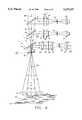
- FIG. 2shows the optical system in a preferred embodiment of the present invention.
- a scanner and the translation stageis used.
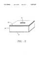
- FIG. 3shows an enlarged view of the aperture plate.
- FIG. 4shows another embodiment of the single aperture portion of FIG. 2.
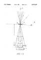
- FIG. 5is a further embodiment of the present invention showing the single aperture and the tilt angle.
- FIG. 6shows another embodiment of the present invention in a confocal fluorescence scanner.
- the image point on the objectis changed by moving the translation stage.
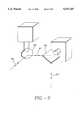
- FIG. 7shows a close-up isometric view of the scanner and its image reflector plates used in the embodiment of FIG. 2.
- An embodiment 10 of the present inventionis incorporated in the optical system of microscope 11 as shown in FIG. 1.
- microscope 11Two well-known examples of microscope 11 are the Nikon Diaphot Inverted microscope and the Nikon Optiphot 2 microscope.
- the optical systemincludes a light source 20 such as a laser, a laser power supply 24 to power the laser, and an optical fiber 23 to guide the laser beam into microscope 11 through light entrance aperture 55.
- a computer system 13provides processing and storage of the various x-y-z confocal images of object 70.
- the object 70rests on movable mechanical translation stage 72.
- FIG. 2will be used to describe the operation of an embodiment of the present invention. Use of light paths 80-88 will facilitate the understanding of the discussion.
- Light source 20provides the necessary light to illuminate each x-y-z image of object 70. Usually, the light from the light source is made up of more than one wavelength.
- the light sourcemay be a laser, a Xenon arc lamp, or any other well known light source.
- Optical fiber 23may be a single-mode optical fiber. Thus, light exiling the optical fiber 23 has a well-defined far-field distribution. Optical fiber 23 acts as a natural spatial filter; therefore, light entrance aperture 55 becomes redundant. The optical fiber 23 also serves as a transmission medium to guide the light from a remote location, if desired, to the optical system. By locating the light source 20 remotely, heat generated by the light source 20 does not affect the performance of the system.
- the first light path 80is between light entrance aperture 55 and dichroic mirror, or beam splitter, 41. After the light is pre-conditioned at light entrance aperture 55 or at the output of optical fiber 23, it then travels to collimating lens 30 which transforms the light so that the light beams run parallel to each other. These parallel light beams encounter an excitation filter 44.
- the collimating lens 30may be replaced with a cylindrical lens to accept light from a pre-conditioning slit aperture serving as light entrance aperture 55.
- the excitation filter 44passes light of only a range of pre-determined wavelengths.
- the type of excitation filter useddictates the wavelength or wavelengths passed.
- Focusing lens 32focuses the light toward a beam splitter 41.
- the beam splitter 41reflects incident light with a particular wavelength toward aperture plate 50 while transmitting along light path 84 return light, such as fluorescent light from the object, with a different range of wavelengths.
- the excitation filter 44may be replaced by a polarizer.
- the beam splitter 41directs the focused light toward aperture 51 on aperture plate 50 along light path 81.
- FIG. 3shows an enlarged view of the aperture plate 50.
- the aperture plate 50is made of a transparent substrate, such as glass, coated on one side 52 with an opaque film such as chromium or aluminum.
- a clear region 51which will serve as an aperture on aperture plate 50 is patterned on the film. Light can pass only through the clear region of the aperture plate 50.
- the aperturemay be a hole in the physical aperture plate.
- the two surfaces of the aperture plate 50must be optically flat to control undesired reflections from the surfaces.
- the two surfacesshould also be unparallel to minimize interference between the surfaces.
- the clear aperturecan be of different shapes for different applications such as a circular pinhole, rectangular hole, a slit, or any desired shape.
- aperture 55To reduce the reflection from the aperture plate 50, light entrance aperture 55 must match the clear region, aperture 51, of the aperture plate 50 so that an image of aperture 55 forms within the aperture 51. Thus, minimum light is reflected from the opaque region of the aperture plate 50 and maximum light passes through aperture 51.
- Lightthen travels to reflecting mirror 40 which is angled to direct the light toward the Galvanometer scanner 60 along light path 82.
- lightpasses through collimating lens 31 toward Galvanometer scanner 60.
- lighttravels toward two scanning image reflector plates 62 and 63.
- the orientation of image reflector plates 62 and 63 with respect to the light and to each otherdetermines the precise x-y (z is constant) image coordinate scanned.
- the light paths 82 and 83are as shown in FIG. 2. However, the spacing and the angular orientation of the image reflector plates 62, 63 create another light path 91.
- the image point 71 on the object 70may be varied along the y-axis.
- the image point 71 on the object 70may be varied along the x-axis.
- the embodiment of FIG. 2shows that the mechanical translation stage 72 may be moved up or down to change the location of the image point 71 on the object 70.
- the scanner 60 and the translation stage 72may be used to position the x-y-z coordinates of the image point 71 on the object 70.
- the objective 34may be moved up or down to change the location of the image point 71 on the object 70.
- the translation stage alone, without a scannercan be moved laterally and vertically to locate the image point 71 on any practically realizable x-y-z coordinate on the object 70.
- the image reflector plates 62 and 63direct light toward scan lens 33, objective 34, and object 70. Because the light is focused on an image point 71 on the object 70, an image of that image point 71 on the object 70 may be acquired and stored.
- apertures 51 of different sizes or shapesmay be mounted on a sliding mechanism such as a dovetail slider and thus allow users to switch among these apertures without realignment.
- beam splitters of different spectral characteristicsmay be mounted on a sliding mechanism and thus allow users to switch among these beam splitters without additional alignment.
- Beam splitter 42directs a portion of the light along light path 86 and another portion along light path 85.
- beam splitter 43directs a portion of the light from the beam splitter 42 toward the direction along light path 87 and another portion of the light, if desired, may be directed along light path 88.
- beam splittersmay be installed in a cascade fashion, if desired, by placing them along light path 88. Beam splitters 42 and 43 each divide the incident beam of light into two beams of equal or different spectral composition but propagating in two different directions.
- Light traveling along light paths 86 and 87encounter barrier filters 45 and 46, respectively, where only a certain range of wavelengths passes through. For example, although light with wavelength 488 nm pass through excitation filter 44, only light with wavelengths 520-560 nm pass through barrier filter 45 and light with wavelength greater than 580 nm pass through barrier filter 46.
- the light passing through filters 45, 46are focused by lenses 37, 38, pre-conditioned by light exit apertures 56, 57 and then collected by sensors 21, 22.
- the scattered light from the aperture plate 50is significantly removed by light stops 58, 59.
- multimode optical fibers 26 and 27may be used to guide and transfer the light to these sensors.
- the finite size of the optical fibers 26 and 27also serves as an aperture to reject scattered light from the system.
- light stops 58, 59become redundant.
- the sensors 21 and 22may be placed close to the electronic portions of the system to minimize electronic noise.
- Light exit apertures 56, 57 or the input ends of optical fiber 26, 27are matched to aperture 51 so that images formed in aperture 51 also form within light exit apertures 56, 57 or the input ends of optical fibers 26, 27. As a result, maximum signal reaches sensors 21, 22 and minimum scattered light passes through.
- barrier filters 45 and 46are particularly useful in fluorescence applications.
- Fluorescent materialemits radiation of a particular wavelength or range of wavelengths when it is excited by an incident energy.
- the wavelength of the incident energyis normally different from that of the fluorescent light.
- incident light from image reflector plates 62 and 63 traveling toward object 70may have wavelength of 488 nm, but the return fluorescent light from the object 70 may have a wavelength of, for example, 520-560 nm. If different fluorescent materials were used on the same object 70, the returning fluorescent light will possess the wavelengths for each of the fluorescent materials.
- an excitation filterfor these fluorescence applications, the use of an excitation filter, a dichroic minor (or beam splitter), and a barrier filter along light paths 86 or 87 of FIG. 2 can be used to further reduce the scattered light from the aperture plate 50.
- the parameters of the excitation and barrier filtersare selected so that minimal overlap between the transparent spectral regions of the two filters exist.
- the aperture plate 50may be tilted at an angle ⁇ from a plane normal to light path 81. This minimizes interference due to reflection from the surface of the aperture plate 50. Thus, little reflected light from the surface of the aperture plate 50 is directed toward beam splitter 41 and light path 84 to interfere with the desired returning light of the image point 71 on the object 70 of FIG. 2. With the aid of the tilt, any further reflection from the surface of the aperture plate can now be blocked with a light stop.
- the angle ⁇must not be too high, such as 90 degrees, or else useful light could not pass through the aperture 51. Furthermore, the angle ⁇ should not be too low, such as ⁇ degrees, and thus defeat the purpose of the fit.
- a typical angleis between 3 to 6 degrees.
- one method of calculating the tilt angle ⁇is as follows. Let D represent the diameter of the entrance pupil of the objective lens 34 and L represents the distance from the intersection of fight path 81 with the plane 89 normal to the light path 81 at the location of aperture 51. Then, ##EQU1## where ⁇ 2 is the subtense angle of the entrance pupil of the objective lens to the aperture plate 50. The angle ⁇ should be:
- ⁇ 1is the convergent angle of the incident beam on the aperture plate.
- the size of the aperture 51 on aperture plate 50is also an important parameter in reducing the negative effects of interference from scattered and reflected light.
- the various filter, lens, and beam splitters along light path 80provide the spatial filtering, shaping, pre-conditioning, or a combination thereof for a high numerical aperture (N.A.) to focus the incident light to a diffraction-limited spot within aperture 51. This spot is significantly smaller than the size of the aperture 51. Thus, the incident light may pass through the aperture without any obstruction.
- N.A.numerical aperture
- the aperture 51acts as a one-way spatial filter in the return light path.
- ⁇wavelength of incoming light
- ⁇ 2 /2maximum half-angle with respect to the axis of the incoming light path.
- N.A.numerical aperture
- ⁇ r ithe lateral extensions ⁇ r i shows that for a large N.A., the focal spot is small. For a small N.A. the focal spot is relatively larger.
- the diameter of the aperture, ashould satisfy the following: ##EQU4##
- the two surfaces, 52 and 53, of FIG. 4must be optically flat. With optically flat surfaces, the reflection of the light from the surfaces is predictable and thus, controllable.
- tilting of the aperture platecan direct undesired surface reflected light in a direction where such light is less harmful.
- the convenient placement of light stops or other light absorbing component in the direction of the controlled reflected lightmay minimize these interferences.
- the two surfaces, 52 and 53can be made unparallel to each other. Such a configuration is shown in FIG. 4.
- Anti-reflection coatingmay also be applied to various surfaces of the optical system to minimize negative effects from surface reflections.
- Opaque film, such as Chromeon surface 52 of the aperture plate 50 may be further coated with an anti-reflection coating, such as Chrome Oxide or Chrome Nitride.
- the clear region on the patterned side and the opposite surface 53 of the aperture plate 50should be coated with a broadband anti-reflection coating to reduce light loss through the substrate and to reduce multiple reflections of light or interference between the two opposite surfaces of the aperture plate
- FIG. 6shows another embodiment of the present invention.
- this embodimentis particularly suited as a confocal fluorescence scanner.
- Light 90 from the light sourcesuch as a laser or arc lamp is first focused to light entrance aperture 55 with focusing lens 39.
- the light passing through the aperture 55is then collimated by a collimating lens 30 and filtered by the excitation filter 44.
- Focusing lens 32focuses the filtered light along path 80 toward dichroic mirror 41, which redirects the beam along path 81 to aperture 51 on aperture plate 50.
- the light passing through the aperture 51is focused by an objective lens 34 to a image point 71 on object 70 containing fluorescent marked materials.
- the object 70can be a fluorescence tagged nucleic acid or polypeptide in a gel slab or in capillary tubes.
- the fluorescence light from the object 70is collected by the objective 34 and is focused back onto the aperture plate along light path 82.
- the light returning back through the aperture 51travels through dichroic mirror 41 along path 84.
- Dichroic mirror 42splits the light into two paths 85 and 86 of different spectral composition.
- dichroic minor 43splits the light along light path 85 into light path 87 and 88.
- Several dichroic mirrorsmay be installed in a cascaded fashion, if desired, by placing them along light path 88. Light traveling along path 86, 87 encounter barrier filters 45, 46, respectively. Only light of desired range of wavelengths pass through the barrier filters 45 and 46.
- Lenses 37 and 38focus the light from filters 45, 46 to light exit aperture 56, 57 and collected by sensors 21, 22.
- either the dichroic mirrors 42, 43 or barrier filters 45, 46 or the two sets in combinationdetermine the range of wavelengths that ultimately pass to the sensors 21, 22.
- Each sensoronly detects light of limited range of wavelengths. So fluorescence light from the object 70 can be separated into its spectral constituents through the optical system and detected by sensors 21, 22. The relative intensity of the spectral constituents reveals the property of the object.
- the object 70may be mounted on a mechanical translation stage 72, which can move the object in the x, y, and z directions and hence change the location of the image point 71 on the object 70.
- a mechanical translation stage 72which can move the object in the x, y, and z directions and hence change the location of the image point 71 on the object 70.
- the objectcan be a fluorescence tagged nucleic acid or polypeptide in a gel slab or in capillary tubes. Scanning the sample relative to the image point 71 produces a map of the fluorescence properties of the object.
- interference due to scattered and reflected lightmay be minimized by tilting the aperture plate, making the two major surfaces of the aperture plate optically flat, coating the aperture plate surfaces with -reflective coating, making the two major surfaces of the aperture plate unparallel, sizing the aperture properly, matching the entrance aperture and exit apertures with the aperture 51, and use of light stops 57, 58 to reject scattered light from aperture plate 50.
Landscapes
- Physics & Mathematics (AREA)
- Chemical & Material Sciences (AREA)
- Analytical Chemistry (AREA)
- General Physics & Mathematics (AREA)
- Optics & Photonics (AREA)
- Health & Medical Sciences (AREA)
- Nuclear Medicine, Radiotherapy & Molecular Imaging (AREA)
- Life Sciences & Earth Sciences (AREA)
- Biochemistry (AREA)
- General Health & Medical Sciences (AREA)
- Immunology (AREA)
- Pathology (AREA)
- Spectroscopy & Molecular Physics (AREA)
- Microscoopes, Condenser (AREA)
Abstract
Description
90°>θ>1/4(α.sub.1 +α.sub.2)
Claims (29)
Priority Applications (1)
| Application Number | Priority Date | Filing Date | Title |
|---|---|---|---|
| US08/213,977US5537247A (en) | 1994-03-15 | 1994-03-15 | Single aperture confocal imaging system |
Applications Claiming Priority (1)
| Application Number | Priority Date | Filing Date | Title |
|---|---|---|---|
| US08/213,977US5537247A (en) | 1994-03-15 | 1994-03-15 | Single aperture confocal imaging system |
Publications (1)
| Publication Number | Publication Date |
|---|---|
| US5537247Atrue US5537247A (en) | 1996-07-16 |
Family
ID=22797281
Family Applications (1)
| Application Number | Title | Priority Date | Filing Date |
|---|---|---|---|
| US08/213,977Expired - LifetimeUS5537247A (en) | 1994-03-15 | 1994-03-15 | Single aperture confocal imaging system |
Country Status (1)
| Country | Link |
|---|---|
| US (1) | US5537247A (en) |
Cited By (38)
| Publication number | Priority date | Publication date | Assignee | Title |
|---|---|---|---|---|
| EP0859250A1 (en)* | 1997-02-13 | 1998-08-19 | Applied Materials, Inc. | Bandpass photon detector |
| WO1999035527A1 (en)* | 1998-01-12 | 1999-07-15 | Wallac Oy | Confocal microscope with plural scanning beams |
| US5932871A (en)* | 1995-11-08 | 1999-08-03 | Olympus Optical Co., Ltd. | Microscope having a confocal point and a non-confocal point, and a confocal point detect method applied thereto |
| WO1999039165A1 (en)* | 1998-01-29 | 1999-08-05 | Leica Microsystems Heidelberg Gmbh | Optical arrangement provided for a spectral fanning out of a light beam |
| GB2342160A (en)* | 1998-09-30 | 2000-04-05 | Ando Electric | Electrooptic probe |
| US6091496A (en)* | 1997-01-28 | 2000-07-18 | Zetetic Institute | Multiple layer, multiple track optical disk access by confocal interference microscopy using wavenumber domain reflectometry and background amplitude reduction and compensation |
| WO2000067062A1 (en)* | 1999-05-05 | 2000-11-09 | Genomic Solutions Inc. | Laser-based optical scanning system |
| US6282020B1 (en)* | 1999-10-21 | 2001-08-28 | Nikon Corporation | Laser microscope and confocal laser scanning microscope |
| US6353216B1 (en)* | 1996-04-25 | 2002-03-05 | Creoscitex Corporation Ltd. | Confocal measurement and diagnostic system |
| US6407838B1 (en)* | 1999-07-21 | 2002-06-18 | Luxn, Inc. | Reconfigurable multi-add/drop module for optical communications |
| US6462814B1 (en) | 2000-03-15 | 2002-10-08 | Schlumberger Technologies, Inc. | Beam delivery and imaging for optical probing of a device operating under electrical test |
| US6480285B1 (en) | 1997-01-28 | 2002-11-12 | Zetetic Institute | Multiple layer confocal interference microscopy using wavenumber domain reflectometry and background amplitude reduction and compensation |
| US6654166B2 (en)* | 2000-06-17 | 2003-11-25 | Leica Microsystems Heidelberg Gmbh | Scanning microscope with multiband illumination and optical component for a scanning microscope with multiband illumination |
| US6674058B1 (en) | 2000-09-20 | 2004-01-06 | Compucyte Corporation | Apparatus and method for focusing a laser scanning cytometer |
| US6717725B2 (en)* | 2000-08-03 | 2004-04-06 | Leica Microsystems Wetzlar Gmbh | Automated microscope system |
| US20040101306A1 (en)* | 2002-08-15 | 2004-05-27 | Hoya Corporation | Optical module |
| US20040190133A1 (en)* | 2001-04-26 | 2004-09-30 | Leica Microsystems Heidelberg Gmbh | Scanning microscope and coupling-out element |
| US6888148B2 (en)* | 2001-12-10 | 2005-05-03 | Carl Zeiss Jena Gmbh | Arrangement for the optical capture of excited and /or back scattered light beam in a sample |
| US6898367B2 (en) | 2000-06-17 | 2005-05-24 | Leica Microsystems Heidelberg Gmbh | Method and instrument for microscopy |
| US20050111089A1 (en)* | 1994-07-15 | 2005-05-26 | Baer Stephen C. | Superresolving microscopy apparatus |
| US20050122580A1 (en)* | 2000-06-17 | 2005-06-09 | Leica Microsystems Heidelberg Gmbh | Arrangement for examining microscopic preparations with a scanning microscope, and illumination device for a scanning microscope |
| US20050174085A1 (en)* | 2004-02-10 | 2005-08-11 | Olympus Corporation | Micromanipulation system |
| EP1610117A3 (en)* | 1997-02-24 | 2006-05-10 | Bodenseewerk Perkin-Elmer Gmbh | Light scanning device |
| US20070002434A1 (en)* | 2003-02-27 | 2007-01-04 | Rimbydas Juskaitis | Microscopic imaging system having an optical correcting element |
| US20090086315A1 (en)* | 2000-06-17 | 2009-04-02 | Leica Microsystem Cms Gmbh | Arrangement for examining microscopic preparations with a scanning microscope, and illumination device for a scanning microscope |
| US20090259446A1 (en)* | 2008-04-10 | 2009-10-15 | Schlumberger Technology Corporation | Method to generate numerical pseudocores using borehole images, digital rock samples, and multi-point statistics |
| US20090295414A1 (en)* | 2008-06-02 | 2009-12-03 | Falk R Aaron | Transient emission scanning microscopy |
| WO2010011953A1 (en)* | 2008-07-25 | 2010-01-28 | Sloan Kettering Institute For Cancer Research | Rapid confocal microscopy to support surgical procedures |
| US20110004447A1 (en)* | 2009-07-01 | 2011-01-06 | Schlumberger Technology Corporation | Method to build 3D digital models of porous media using transmitted laser scanning confocal mircoscopy and multi-point statistics |
| US20110004448A1 (en)* | 2009-07-01 | 2011-01-06 | Schlumberger Technology Corporation | Method to quantify discrete pore shapes, volumes, and surface areas using confocal profilometry |
| US20120085929A1 (en)* | 2005-11-14 | 2012-04-12 | Peter Westphal | Multispectral Illumination Device |
| WO2013131808A1 (en)* | 2012-03-09 | 2013-09-12 | Carl Zeiss Microscopy Gmbh | Light scanning microscope with spectral detection |
| JP2017003864A (en)* | 2015-06-12 | 2017-01-05 | オリンパス株式会社 | Microscope system |
| US9581723B2 (en) | 2008-04-10 | 2017-02-28 | Schlumberger Technology Corporation | Method for characterizing a geological formation traversed by a borehole |
| US9638909B2 (en) | 2006-12-22 | 2017-05-02 | Isis Innovation Limited | Focusing apparatus and method |
| US20180094975A1 (en)* | 2016-10-04 | 2018-04-05 | Precitec Optronik Gmbh | Chromatic confocal distance sensor |
| US20210306564A1 (en)* | 2019-08-08 | 2021-09-30 | Massachusetts Institute Of Technology | Ultra-Wide Field-of-View Flat Optics |
| US20220026730A1 (en)* | 2018-12-11 | 2022-01-27 | Safran Electronics & Defense | Multispectral harmonisation device intended for aligning the optical channels of an optronic system |
Citations (19)
| Publication number | Priority date | Publication date | Assignee | Title |
|---|---|---|---|---|
| US3013467A (en)* | 1957-11-07 | 1961-12-19 | Minsky Marvin | Microscopy apparatus |
| US3517980A (en)* | 1966-12-05 | 1970-06-30 | Ceskoslovenska Akademie Ved | Method and arrangement for improving the resolving power and contrast |
| US3547512A (en)* | 1968-04-16 | 1970-12-15 | Research Corp | Optical apparatus providing focalplane-specific illumination |
| US3926500A (en)* | 1974-12-02 | 1975-12-16 | Ibm | Method of increasing the depth of focus and or the resolution of light microscopes by illuminating and imaging through a diaphragm with pinhole apertures |
| US4062623A (en)* | 1975-04-07 | 1977-12-13 | Canon Kabushiki Kaisha | Device for observing an object |
| US4170398A (en)* | 1978-05-03 | 1979-10-09 | Koester Charles J | Scanning microscopic apparatus with three synchronously rotating reflecting surfaces |
| US4198571A (en)* | 1977-04-28 | 1980-04-15 | National Research Development Corporation | Scanning microscopes |
| US4251129A (en)* | 1977-10-05 | 1981-02-17 | Canon Kabushiki Kaisha | Photoelectric detecting device |
| US4689491A (en)* | 1985-04-19 | 1987-08-25 | Datasonics Corp. | Semiconductor wafer scanning system |
| US4884881A (en)* | 1987-11-16 | 1989-12-05 | Washington University | Single aperture confocal scanning epi-illumination microscope |
| US4884880A (en)* | 1987-11-16 | 1989-12-05 | Washington University | Kit for converting a standard microscope into a single aperture confocal scanning epi-illumination microscope |
| US4919516A (en)* | 1987-07-24 | 1990-04-24 | Jednotne Zemedelske Druzstvo "Vitezny Unor" Se Sidlem V Komorne | Optical tandem scanning system using a koesters reflecting prism for light splitting |
| US4927254A (en)* | 1987-03-27 | 1990-05-22 | The Board Of Trustees Of The Leland Stanford Junior University | Scanning confocal optical microscope including an angled apertured rotating disc placed between a pinhole and an objective lens |
| US4965441A (en)* | 1988-01-27 | 1990-10-23 | Commissariat A L'energie Atomique | Method for the scanning confocal light-optical microscopic and indepth examination of an extended field and devices for implementing said method |
| US5022743A (en)* | 1987-03-27 | 1991-06-11 | The Board Of Trustees Of The Leland Stanford Junior University | Scanning confocal optical microscope |
| US5091652A (en)* | 1990-01-12 | 1992-02-25 | The Regents Of The University Of California | Laser excited confocal microscope fluorescence scanner and method |
| US5101295A (en)* | 1988-09-14 | 1992-03-31 | Washington University | Rotating slit aperture for scanning microscopy |
| US5132526A (en)* | 1990-04-10 | 1992-07-21 | Fuji Photo Film Co., Ltd. | Confocal scanning microscope having a signal output regulating means |
| US5448350A (en)* | 1990-07-19 | 1995-09-05 | Canon Kabushiki Kaisha | Surface state inspection apparatus and exposure apparatus including the same |
- 1994
- 1994-03-15USUS08/213,977patent/US5537247A/ennot_activeExpired - Lifetime
Patent Citations (19)
| Publication number | Priority date | Publication date | Assignee | Title |
|---|---|---|---|---|
| US3013467A (en)* | 1957-11-07 | 1961-12-19 | Minsky Marvin | Microscopy apparatus |
| US3517980A (en)* | 1966-12-05 | 1970-06-30 | Ceskoslovenska Akademie Ved | Method and arrangement for improving the resolving power and contrast |
| US3547512A (en)* | 1968-04-16 | 1970-12-15 | Research Corp | Optical apparatus providing focalplane-specific illumination |
| US3926500A (en)* | 1974-12-02 | 1975-12-16 | Ibm | Method of increasing the depth of focus and or the resolution of light microscopes by illuminating and imaging through a diaphragm with pinhole apertures |
| US4062623A (en)* | 1975-04-07 | 1977-12-13 | Canon Kabushiki Kaisha | Device for observing an object |
| US4198571A (en)* | 1977-04-28 | 1980-04-15 | National Research Development Corporation | Scanning microscopes |
| US4251129A (en)* | 1977-10-05 | 1981-02-17 | Canon Kabushiki Kaisha | Photoelectric detecting device |
| US4170398A (en)* | 1978-05-03 | 1979-10-09 | Koester Charles J | Scanning microscopic apparatus with three synchronously rotating reflecting surfaces |
| US4689491A (en)* | 1985-04-19 | 1987-08-25 | Datasonics Corp. | Semiconductor wafer scanning system |
| US4927254A (en)* | 1987-03-27 | 1990-05-22 | The Board Of Trustees Of The Leland Stanford Junior University | Scanning confocal optical microscope including an angled apertured rotating disc placed between a pinhole and an objective lens |
| US5022743A (en)* | 1987-03-27 | 1991-06-11 | The Board Of Trustees Of The Leland Stanford Junior University | Scanning confocal optical microscope |
| US4919516A (en)* | 1987-07-24 | 1990-04-24 | Jednotne Zemedelske Druzstvo "Vitezny Unor" Se Sidlem V Komorne | Optical tandem scanning system using a koesters reflecting prism for light splitting |
| US4884881A (en)* | 1987-11-16 | 1989-12-05 | Washington University | Single aperture confocal scanning epi-illumination microscope |
| US4884880A (en)* | 1987-11-16 | 1989-12-05 | Washington University | Kit for converting a standard microscope into a single aperture confocal scanning epi-illumination microscope |
| US4965441A (en)* | 1988-01-27 | 1990-10-23 | Commissariat A L'energie Atomique | Method for the scanning confocal light-optical microscopic and indepth examination of an extended field and devices for implementing said method |
| US5101295A (en)* | 1988-09-14 | 1992-03-31 | Washington University | Rotating slit aperture for scanning microscopy |
| US5091652A (en)* | 1990-01-12 | 1992-02-25 | The Regents Of The University Of California | Laser excited confocal microscope fluorescence scanner and method |
| US5132526A (en)* | 1990-04-10 | 1992-07-21 | Fuji Photo Film Co., Ltd. | Confocal scanning microscope having a signal output regulating means |
| US5448350A (en)* | 1990-07-19 | 1995-09-05 | Canon Kabushiki Kaisha | Surface state inspection apparatus and exposure apparatus including the same |
Cited By (61)
| Publication number | Priority date | Publication date | Assignee | Title |
|---|---|---|---|---|
| US20050111089A1 (en)* | 1994-07-15 | 2005-05-26 | Baer Stephen C. | Superresolving microscopy apparatus |
| US5932871A (en)* | 1995-11-08 | 1999-08-03 | Olympus Optical Co., Ltd. | Microscope having a confocal point and a non-confocal point, and a confocal point detect method applied thereto |
| US6353216B1 (en)* | 1996-04-25 | 2002-03-05 | Creoscitex Corporation Ltd. | Confocal measurement and diagnostic system |
| US6480285B1 (en) | 1997-01-28 | 2002-11-12 | Zetetic Institute | Multiple layer confocal interference microscopy using wavenumber domain reflectometry and background amplitude reduction and compensation |
| US6091496A (en)* | 1997-01-28 | 2000-07-18 | Zetetic Institute | Multiple layer, multiple track optical disk access by confocal interference microscopy using wavenumber domain reflectometry and background amplitude reduction and compensation |
| US5995235A (en)* | 1997-02-13 | 1999-11-30 | Applied Materials, Inc. | Bandpass photon detector |
| EP0859250A1 (en)* | 1997-02-13 | 1998-08-19 | Applied Materials, Inc. | Bandpass photon detector |
| EP1610117A3 (en)* | 1997-02-24 | 2006-05-10 | Bodenseewerk Perkin-Elmer Gmbh | Light scanning device |
| WO1999035527A1 (en)* | 1998-01-12 | 1999-07-15 | Wallac Oy | Confocal microscope with plural scanning beams |
| WO1999039165A1 (en)* | 1998-01-29 | 1999-08-05 | Leica Microsystems Heidelberg Gmbh | Optical arrangement provided for a spectral fanning out of a light beam |
| US6801359B1 (en) | 1998-01-29 | 2004-10-05 | Leica Microsystems Heidelberg Gmbh | Optical arrangement provided for a spectral fanning out of a light beam |
| GB2342160B (en)* | 1998-09-30 | 2000-12-13 | Ando Electric | Electro-optic probe |
| GB2342160A (en)* | 1998-09-30 | 2000-04-05 | Ando Electric | Electrooptic probe |
| WO2000067062A1 (en)* | 1999-05-05 | 2000-11-09 | Genomic Solutions Inc. | Laser-based optical scanning system |
| US6407838B1 (en)* | 1999-07-21 | 2002-06-18 | Luxn, Inc. | Reconfigurable multi-add/drop module for optical communications |
| US6282020B1 (en)* | 1999-10-21 | 2001-08-28 | Nikon Corporation | Laser microscope and confocal laser scanning microscope |
| US6462814B1 (en) | 2000-03-15 | 2002-10-08 | Schlumberger Technologies, Inc. | Beam delivery and imaging for optical probing of a device operating under electrical test |
| US20090086315A1 (en)* | 2000-06-17 | 2009-04-02 | Leica Microsystem Cms Gmbh | Arrangement for examining microscopic preparations with a scanning microscope, and illumination device for a scanning microscope |
| US20070035822A1 (en)* | 2000-06-17 | 2007-02-15 | Leica Microsystems Cms Gmbh | Arrangement for examining microscopic preparations with a scanning microscope, and illumination device for a scanning microscope |
| US7679822B2 (en) | 2000-06-17 | 2010-03-16 | Leica Microsystems Cms Gmbh | Broadband laser illumination device for a scanning microscope with output stabilization |
| US7123408B2 (en) | 2000-06-17 | 2006-10-17 | Leica Microsystems Cms Gmbh | Arrangement for examining microscopic preparations with a scanning microscope, and illumination device for a scanning microscope |
| US6898367B2 (en) | 2000-06-17 | 2005-05-24 | Leica Microsystems Heidelberg Gmbh | Method and instrument for microscopy |
| US6654166B2 (en)* | 2000-06-17 | 2003-11-25 | Leica Microsystems Heidelberg Gmbh | Scanning microscope with multiband illumination and optical component for a scanning microscope with multiband illumination |
| US20050111816A1 (en)* | 2000-06-17 | 2005-05-26 | Leica Microsystems Heidelberg Gmbh | Method and instrument for microscopy |
| US20050122580A1 (en)* | 2000-06-17 | 2005-06-09 | Leica Microsystems Heidelberg Gmbh | Arrangement for examining microscopic preparations with a scanning microscope, and illumination device for a scanning microscope |
| US7110645B2 (en) | 2000-06-17 | 2006-09-19 | Leica Microsystems Cms Gmbh | Method and instrument for microscopy |
| US6717725B2 (en)* | 2000-08-03 | 2004-04-06 | Leica Microsystems Wetzlar Gmbh | Automated microscope system |
| US6674058B1 (en) | 2000-09-20 | 2004-01-06 | Compucyte Corporation | Apparatus and method for focusing a laser scanning cytometer |
| US6977773B2 (en)* | 2001-04-26 | 2005-12-20 | Leica Microsystems Heidelberg Gmbh | Scanning microscope and coupling-out element |
| US20040190133A1 (en)* | 2001-04-26 | 2004-09-30 | Leica Microsystems Heidelberg Gmbh | Scanning microscope and coupling-out element |
| US6888148B2 (en)* | 2001-12-10 | 2005-05-03 | Carl Zeiss Jena Gmbh | Arrangement for the optical capture of excited and /or back scattered light beam in a sample |
| US20040101306A1 (en)* | 2002-08-15 | 2004-05-27 | Hoya Corporation | Optical module |
| US7215853B2 (en)* | 2002-08-15 | 2007-05-08 | Hoya Corporation | Optical module formed on common substrate for branching an optical signal |
| US7476831B2 (en)* | 2003-02-27 | 2009-01-13 | Isis Innovation Limited | Microscopic imaging system having an optical correcting element |
| US20070002434A1 (en)* | 2003-02-27 | 2007-01-04 | Rimbydas Juskaitis | Microscopic imaging system having an optical correcting element |
| US20050174085A1 (en)* | 2004-02-10 | 2005-08-11 | Olympus Corporation | Micromanipulation system |
| US20120085929A1 (en)* | 2005-11-14 | 2012-04-12 | Peter Westphal | Multispectral Illumination Device |
| US9239293B2 (en) | 2005-11-14 | 2016-01-19 | Carl Zeiss Microscopy Gmbh | Multispectral illumination device |
| US8610088B2 (en)* | 2005-11-14 | 2013-12-17 | Carl Zeiss Microscopy Gmbh | Multispectral illumination device |
| US9638909B2 (en) | 2006-12-22 | 2017-05-02 | Isis Innovation Limited | Focusing apparatus and method |
| US20090259446A1 (en)* | 2008-04-10 | 2009-10-15 | Schlumberger Technology Corporation | Method to generate numerical pseudocores using borehole images, digital rock samples, and multi-point statistics |
| US9581723B2 (en) | 2008-04-10 | 2017-02-28 | Schlumberger Technology Corporation | Method for characterizing a geological formation traversed by a borehole |
| US8725477B2 (en) | 2008-04-10 | 2014-05-13 | Schlumberger Technology Corporation | Method to generate numerical pseudocores using borehole images, digital rock samples, and multi-point statistics |
| US7952374B2 (en)* | 2008-06-02 | 2011-05-31 | Quantum Focus Instruments Corporation | Transient emission scanning microscopy |
| US20090295414A1 (en)* | 2008-06-02 | 2009-12-03 | Falk R Aaron | Transient emission scanning microscopy |
| WO2010011953A1 (en)* | 2008-07-25 | 2010-01-28 | Sloan Kettering Institute For Cancer Research | Rapid confocal microscopy to support surgical procedures |
| US10001635B2 (en) | 2008-07-25 | 2018-06-19 | Sloan Kettering Institute For Cancer Research | Rapid confocal microscopy to support surgical procedures |
| US20110116694A1 (en)* | 2008-07-25 | 2011-05-19 | Sloan Kettering Institute For Cancer Research | Rapid confocal microscopy to support surgical procedures |
| US9176310B2 (en) | 2008-07-25 | 2015-11-03 | Sloan Kettering Institute For Cancer Research | Rapid confocal microscopy to support surgical procedures |
| US20110004447A1 (en)* | 2009-07-01 | 2011-01-06 | Schlumberger Technology Corporation | Method to build 3D digital models of porous media using transmitted laser scanning confocal mircoscopy and multi-point statistics |
| US8311788B2 (en) | 2009-07-01 | 2012-11-13 | Schlumberger Technology Corporation | Method to quantify discrete pore shapes, volumes, and surface areas using confocal profilometry |
| US20110004448A1 (en)* | 2009-07-01 | 2011-01-06 | Schlumberger Technology Corporation | Method to quantify discrete pore shapes, volumes, and surface areas using confocal profilometry |
| WO2013131808A1 (en)* | 2012-03-09 | 2013-09-12 | Carl Zeiss Microscopy Gmbh | Light scanning microscope with spectral detection |
| US9989754B2 (en) | 2012-03-09 | 2018-06-05 | Carl Zeiss Microscopy Gmbh | Light scanning microscope with spectral detection |
| JP2017003864A (en)* | 2015-06-12 | 2017-01-05 | オリンパス株式会社 | Microscope system |
| US20180094975A1 (en)* | 2016-10-04 | 2018-04-05 | Precitec Optronik Gmbh | Chromatic confocal distance sensor |
| US10260941B2 (en)* | 2016-10-04 | 2019-04-16 | Precitec Optronik Gmbh | Chromatic confocal distance sensor |
| US20220026730A1 (en)* | 2018-12-11 | 2022-01-27 | Safran Electronics & Defense | Multispectral harmonisation device intended for aligning the optical channels of an optronic system |
| US11740482B2 (en)* | 2018-12-11 | 2023-08-29 | Safran Electronics & Defense | Multispectral harmonisation device intended for aligning the optical channels of an optronic system |
| US20210306564A1 (en)* | 2019-08-08 | 2021-09-30 | Massachusetts Institute Of Technology | Ultra-Wide Field-of-View Flat Optics |
| US12212853B2 (en)* | 2019-08-08 | 2025-01-28 | Massachusetts Institute Of Technology | Ultra-wide field-of-view flat optics |
Similar Documents
| Publication | Publication Date | Title |
|---|---|---|
| US5537247A (en) | Single aperture confocal imaging system | |
| CA1325537C (en) | Confocal microscope | |
| US4653880A (en) | Reflective beam splitting objective | |
| JP3385432B2 (en) | Inspection device | |
| US7348528B2 (en) | Distance measuring system | |
| US6987609B2 (en) | Microscope | |
| US5225671A (en) | Confocal optical apparatus | |
| JP2019133176A (en) | Deep ultraviolet, continuous wave laser, system, and method | |
| US5288987A (en) | Autofocusing arrangement for a stereomicroscope which permits automatic focusing on objects on which reflections occur | |
| US7554726B2 (en) | Objective for evanescent illumination and microscope | |
| JP2004038139A (en) | Equipment for beam coupling into the microscope | |
| CN110869832A (en) | Optical microscope and method for providing structured illumination light | |
| US20070146724A1 (en) | Vibration-resistant interferometer apparatus | |
| JP5039307B2 (en) | Objective lens and microscope | |
| US6084672A (en) | Device for optically measuring an object using a laser interferometer | |
| KR100207682B1 (en) | Laser Beam Dispersion Compensation Method of Optical Pickup Device | |
| US5317142A (en) | Automatic focusing apparatus which removes light reflected by a lower surface of a sample | |
| US20020097485A1 (en) | Confocal microscope | |
| US7808699B2 (en) | Microscope lens for total internal reflection microscopy and microscope | |
| US5861984A (en) | Confocal scanning microscope and beamsplitter therefor | |
| CN106575030A (en) | Microscope with beam splitter assembly | |
| US4934799A (en) | Multi-lens focussing arrangement for laser graphics imaging apparatus | |
| WO2003060589A1 (en) | Auto focussing device and method | |
| GB2416439A (en) | Laser scanning microscope | |
| US4402602A (en) | Knife edge system |
Legal Events
| Date | Code | Title | Description |
|---|---|---|---|
| AS | Assignment | Owner name:TECHNICAL INSTRUMENT COMPANY, CALIFORNIA Free format text:ASSIGNMENT OF ASSIGNORS INTEREST;ASSIGNOR:XIAO, GUOQUING;REEL/FRAME:006992/0718 Effective date:19940314 | |
| AS | Assignment | Owner name:SILICON VALLEY BANK, CALIFORNIA Free format text:SECURITY INTEREST;ASSIGNOR:TECHNICAL INSTRUMENTS COMPANY;REEL/FRAME:007204/0739 Effective date:19940715 | |
| STCF | Information on status: patent grant | Free format text:PATENTED CASE | |
| FEPP | Fee payment procedure | Free format text:PAYOR NUMBER ASSIGNED (ORIGINAL EVENT CODE: ASPN); ENTITY STATUS OF PATENT OWNER: LARGE ENTITY | |
| FPAY | Fee payment | Year of fee payment:4 | |
| FEPP | Fee payment procedure | Free format text:PAT HOLDER NO LONGER CLAIMS SMALL ENTITY STATUS, ENTITY STATUS SET TO UNDISCOUNTED (ORIGINAL EVENT CODE: STOL); ENTITY STATUS OF PATENT OWNER: LARGE ENTITY | |
| FEPP | Fee payment procedure | Free format text:PAYER NUMBER DE-ASSIGNED (ORIGINAL EVENT CODE: RMPN); ENTITY STATUS OF PATENT OWNER: LARGE ENTITY Free format text:PAYOR NUMBER ASSIGNED (ORIGINAL EVENT CODE: ASPN); ENTITY STATUS OF PATENT OWNER: LARGE ENTITY | |
| FPAY | Fee payment | Year of fee payment:8 | |
| FEPP | Fee payment procedure | Free format text:PAYER NUMBER DE-ASSIGNED (ORIGINAL EVENT CODE: RMPN); ENTITY STATUS OF PATENT OWNER: LARGE ENTITY Free format text:PAYOR NUMBER ASSIGNED (ORIGINAL EVENT CODE: ASPN); ENTITY STATUS OF PATENT OWNER: LARGE ENTITY | |
| FPAY | Fee payment | Year of fee payment:12 | |
| REMI | Maintenance fee reminder mailed |