US5537123A - Antennas and antenna units - Google Patents
Antennas and antenna unitsDownload PDFInfo
- Publication number
- US5537123A US5537123AUS08/398,325US39832595AUS5537123AUS 5537123 AUS5537123 AUS 5537123AUS 39832595 AUS39832595 AUS 39832595AUS 5537123 AUS5537123 AUS 5537123A
- Authority
- US
- United States
- Prior art keywords
- electrode
- grounding
- antenna
- base plate
- connector
- Prior art date
- Legal status (The legal status is an assumption and is not a legal conclusion. Google has not performed a legal analysis and makes no representation as to the accuracy of the status listed.)
- Expired - Lifetime
Links
- 239000003990capacitorSubstances0.000claimsdescription10
- 239000004020conductorSubstances0.000claimsdescription8
- 238000007373indentationMethods0.000claimsdescription6
- 238000007667floatingMethods0.000claimsdescription2
- 238000005452bendingMethods0.000abstractdescription3
- 238000010586diagramMethods0.000description2
- 238000010295mobile communicationMethods0.000description2
- 238000005476solderingMethods0.000description2
- RYGMFSIKBFXOCR-UHFFFAOYSA-NCopperChemical compound[Cu]RYGMFSIKBFXOCR-UHFFFAOYSA-N0.000description1
- 229910000881Cu alloyInorganic materials0.000description1
- 230000002411adverseEffects0.000description1
- 230000005540biological transmissionEffects0.000description1
- 229910052802copperInorganic materials0.000description1
- 239000010949copperSubstances0.000description1
- 238000005516engineering processMethods0.000description1
- 238000012986modificationMethods0.000description1
- 230000004048modificationEffects0.000description1
- 229910000679solderInorganic materials0.000description1
Images

Classifications
- H—ELECTRICITY
- H01—ELECTRIC ELEMENTS
- H01Q—ANTENNAS, i.e. RADIO AERIALS
- H01Q9/00—Electrically-short antennas having dimensions not more than twice the operating wavelength and consisting of conductive active radiating elements
- H01Q9/04—Resonant antennas
- H01Q9/0407—Substantially flat resonant element parallel to ground plane, e.g. patch antenna
- H01Q9/0421—Substantially flat resonant element parallel to ground plane, e.g. patch antenna with a shorting wall or a shorting pin at one end of the element
Definitions
- This inventionrelates to antennas and antenna units used for mobile communication systems.
- FIGS. 6A and 6BAn example of prior art microstrip antenna, for use in a mobile communication system such as a car radio, is shown generally at 35 in FIGS. 6A and 6B wherein numeral 31 indicates a dielectric base plate with a patch electrode 32 and a shielding electrode 33 formed on its surfaces.
- a connector 34 with an inner conductor and an outer conductoris attached to the same side of the base plate 31 as the shielding electrode 33, with the inner conductor connected to a feed point 32a of the patch electrode 32 and the outer conductor connected to the shielding electrode 33. Electromagnetic waves are received and transmitted through the patch electrode 32 such that the functions of an antenna can be carried out.
- a metallic chassisis used as the radiating part of the antenna, not only is the resistance of the antenna reduced, but also its capacity is increased and its Joule loss is reduced, thereby increasing its gain. Since the antenna is surface-mounted to a printed circuit board by inserting its metallic chassis into an opening formed in the circuit board, furthermore, the height by which the antenna protrudes from the circuit board can be reduced.
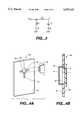
- FIG. 1is a diagonal view of an antenna embodying the invention
- FIG. 2is a diagonal exploded view of the antenna of FIG. 1;
- FIG. 3is an equivalent circuit diagram of the antenna of FIG. 1;
- FIG. 4Ais a diagonal exploded view of an antenna unit embodying the invention and FIG. 4B is a sectional view of the antenna unit of, FIG. 4A when it is assembled;
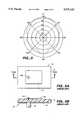
- FIG. 5shows the directional characteristic of the antenna unit of FIGS. 4A and 4B.
- FIG. 6is a plan view of a prior art antenna and FIG. 6B is its sectional view taken along line VI-B-VI-B of FIG. 6A.
- FIGS. 1 and 2show an antenna 18 embodying the present invention comprising a rectangular dielectric base plate 1 with throughholes 1a, 1b and 1c formed therethrough near its shorter edges.
- An input electrode 2 and a connector electrode 3are formed around the throughholes 1a and 1c, respectively, on the base plate 1.
- a grounding conductor 4is also formed on the base plate 1, separated from the input electrode 2 and the connector electrode 3.
- Solder resist ink 5is applied over a large portion of the grounding conductor 4, leaving portions of the grounding conductor 4 exposed to form ground-connecting areas 4a, 4b and 4c(herein referred to as grounding areas) along the two longer edges of the base plate 1, around the throughhole 1b, and on the opposite side of the connector electrode 3, respectively.
- a chip capacitor 6is connected between the connector electrode 3 and the connecting area 4c.
- Numeral 11indicates a metallic chassis made, for example, of copper or a copper alloy. It has a planar rectangular radiating part 12 and two planar attachment parts 13 and 14 formed by bending the two shorter edge portions of the radiating part 12 perpendicularly thereto.
- the attachment part 13has two protrusions 15a and 15b formed unistructurally therewith, and the other attachment part 14 has one protrusion 15c formed unistructurally therewith.
- An indentation 16is formed on the edge of the attachment part 13 between its two protrusions 15a and 15b.
- protrusions 15a, 15b and 15c and throughholes 1a, 1b and 1care formed correspondingly with respect to each other such that the metallic chassis 11 can be attached to the base plate 1 by inserting the three protrusions 15a, 15b and 15b respectively into the throughholes 1a, 1b and 1c and soldering the input electrode 2, the connecting area 4b and the connector electrode 3 with the attachment parts 13 and 14.
- An antenna thus structuredhas the advantage of having smaller resistance because a metallic radiating part 12 is used for transmission and reception of electromagnetic waves. It has an improved gain because its large heat capacity reduces its Joule loss.
- FIG. 3which is an equivalent circuit diagram of the antenna 18, it may be considered to comprise inductance L 1 and L 2 and capacitance C, where the inductance L 1 is primarily that of the radiating part 12 of the metallic chassis 11 and L 2 is the inductance between the input electrode 2 and the connecting area 4b, or primarily between the protrusions 15a and 15b of the attachment part 13 of the metallic chassis 11.
- the capacitance Cis primarily that of the chip capacitor 6 connected between the connector electrode 3 and the connecting area 4c.
- Impedance matching of the antenna 18 with an external circuitcan be carried out easily by changing the impedance of the antenna 18 by varying the dimensions of the indentation 16 such as its width and depth to thereby change the magnitude of the inductance L 2 and to adjust the ratio between L 1 and L 2 .
- FIGS. 4A and 4Bshow an electronic component (referred to as an antenna unit) incorporating an antenna embodying this invention and comprising a printed circuit board 21 having an opening 22 therethrough which is larger than the external contour of the metallic chassis 11 of the antenna 18.
- a pair of grounding electrodes 23is formed on a front surface thereof with one edge abutting the opening 22, and a feed electrode 24 is formed on the same surface with one edge abutting a portion of the opening 22 where the grounding electrodes 23 are not formed.
- the input electrode 2 of the antenna 18is soldered to the feed electrode 24 of the printed circuit board 21, and the connecting areas 4a of the antenna 18 are soldered to the grounding electrodes 23 on the printed circuit board 21 to complete a surface-mounted antenna unit 28.
- an antenna unit as described abovehas been produced with a dielectric base plate of width 8 mm, length 12 mm and thickness 1 mm, a chip capacitor of 1 pF, and a metallic chassis of width 6.3 mm, length 10 mm and height 3 mm, having an antenna of resonance frequency 1.9 GHz attached to a printed circuit board of width 60 mm, length 90 mm and thickness 0.8 mm. Its directional characteristic is shown in FIG. 5, indicating that a maximum gain as high as -1dB was obtained although the maximum length of the antenna was only 1/16 of the wavelength. It is also to be appreciated that the maximum height of the antenna from its printed circuit board was only 2.2 mm.
- antennas and antenna units according to the present inventioncan be made compact because a metallic radiating part 12 is used to reduce its resistance and to increase its heat capacity such that its gain is improved. Since the antenna is surface-mounted by inserting its metallic chassis into an opening provided to a printed circuit board, furthermore, the height of the antenna by which it protrudes from the printed circuit board can be reduced. Moreover, the inductance between its input part and grounding electrode can be easily adjusted by varying the shape of the indentation in the metallic chassis for the antenna such that impedance matching of the antenna with an external circuit can be easily performed for reducing its reflection loss.
Landscapes
- Waveguide Aerials (AREA)
Abstract
Description
Claims (19)
Applications Claiming Priority (2)
| Application Number | Priority Date | Filing Date | Title |
|---|---|---|---|
| JP6040054AJPH07249925A (en) | 1994-03-10 | 1994-03-10 | Antenna and antenna system |
| JP6-040054 | 1994-03-10 |
Publications (1)
| Publication Number | Publication Date |
|---|---|
| US5537123Atrue US5537123A (en) | 1996-07-16 |
Family
ID=12570209
Family Applications (1)
| Application Number | Title | Priority Date | Filing Date |
|---|---|---|---|
| US08/398,325Expired - LifetimeUS5537123A (en) | 1994-03-10 | 1995-03-03 | Antennas and antenna units |
Country Status (2)
| Country | Link |
|---|---|
| US (1) | US5537123A (en) |
| JP (1) | JPH07249925A (en) |
Cited By (32)
| Publication number | Priority date | Publication date | Assignee | Title |
|---|---|---|---|---|
| US5696517A (en)* | 1995-09-28 | 1997-12-09 | Murata Manufacturing Co., Ltd. | Surface mounting antenna and communication apparatus using the same |
| US5831578A (en)* | 1995-09-27 | 1998-11-03 | Compagnie Generale D'automatisme Cga-Hbs | Microwave antenna element |
| US5959582A (en)* | 1996-12-10 | 1999-09-28 | Murata Manufacturing Co., Ltd. | Surface mount type antenna and communication apparatus |
| US5969680A (en)* | 1994-10-11 | 1999-10-19 | Murata Manufacturing Co., Ltd. | Antenna device having a radiating portion provided between a wiring substrate and a case |
| US6215447B1 (en) | 1998-01-16 | 2001-04-10 | Rangestar Wireless, Inc. | Antenna assembly for communications devices |
| US6326927B1 (en) | 1999-07-21 | 2001-12-04 | Range Star Wireless, Inc. | Capacitively-tuned broadband antenna structure |
| US6329960B1 (en) | 2000-06-24 | 2001-12-11 | 3Com Corporation | Antenna assembly |
| US6384786B2 (en)* | 2000-01-13 | 2002-05-07 | Murata Manufacturing Co., Ltd. | Antenna device and communication apparatus |
| WO2002063717A1 (en)* | 2001-02-03 | 2002-08-15 | Robert Bosch Gmbh | Planar antenna |
| US6509882B2 (en) | 1999-12-14 | 2003-01-21 | Tyco Electronics Logistics Ag | Low SAR broadband antenna assembly |
| US6542122B1 (en) | 2001-10-16 | 2003-04-01 | Telefonaktiebolaget Lm Ericsson (Publ) | Patch antenna precision connection |
| WO2003047025A1 (en)* | 2001-11-28 | 2003-06-05 | Koninklijke Philips Electronics N.V. | Dual-band antenna arrangement |
| US6593523B2 (en)* | 2001-01-19 | 2003-07-15 | Mitsubishi Denki Kabushiki Kaisha | Shield structure for electronic circuit parts |
| US6606250B1 (en)* | 2002-06-21 | 2003-08-12 | Global Sun Technology Inc. | Circuit board having a stable L-shaped antenna |
| US20040056806A1 (en)* | 2002-09-20 | 2004-03-25 | Tatung Co., Ltd. | PCB antenna capable of receiving four operating bands |
| WO2004027928A1 (en)* | 2002-09-23 | 2004-04-01 | Telefonaktiebolaget L M Ericsson (Publ) | A planar antenna |
| US6720923B1 (en)* | 2000-09-14 | 2004-04-13 | Stata Labs, Llc | Antenna design utilizing a cavity architecture for global positioning system (GPS) applications |
| EP1418644A1 (en)* | 2002-09-23 | 2004-05-12 | Telefonaktiebolaget LM Ericsson (publ) | A planar antenna |
| US6747601B2 (en)* | 2001-07-21 | 2004-06-08 | Koninklijke Philips Electronics N.V. | Antenna arrangement |
| US20040239564A1 (en)* | 2002-03-28 | 2004-12-02 | Misako Sakae | Antenna and electronic apparatus using it |
| US20050001768A1 (en)* | 2003-05-29 | 2005-01-06 | Masami Sekiguchi | Surface mount antenna, and an antenna element mounting method |
| US20050190543A1 (en)* | 2004-02-26 | 2005-09-01 | Eagle Comtronics, Inc. | Circuit board sub-assemblies, methods for manufacturing same, electronic signal filters including same, and methods, for manufacturing electronic signal filters including same |
| US20050259017A1 (en)* | 2004-05-19 | 2005-11-24 | Korkut Yegin | Dual band loop antenna |
| WO2007110250A1 (en)* | 2006-03-27 | 2007-10-04 | Siemens Aktiengesellschaft | Apparatus having a capacitively or inductively loaded planar antenna |
| US20080234008A1 (en)* | 2007-03-22 | 2008-09-25 | Brother Kogyo Kabushiki Kaisha | Radio-frequency telephone set |
| US20090033570A1 (en)* | 2007-07-30 | 2009-02-05 | High Tech Computer Corp. | Antenna module and electronic device using the same |
| US20110080333A1 (en)* | 2009-10-06 | 2011-04-07 | Min-Chung Wu | Electronic Device with Embedded Antenna |
| TWI416795B (en)* | 2009-10-06 | 2013-11-21 | Ralink Technology Corp | Electronic device with embedded three-dimensional antenna |
| FR3009443A1 (en)* | 2013-08-05 | 2015-02-06 | Insight Sip | DEVICE FOR TRANSMITTING AND / OR RECEIVING RADIO FREQUENCY SIGNALS |
| US20150048998A1 (en)* | 2013-08-16 | 2015-02-19 | Auden Techno Corp. | Metal plate antenna |
| US20150097748A1 (en)* | 2013-10-08 | 2015-04-09 | Pc-Tel, Inc. | Wide band lte antenna |
| US11132593B2 (en) | 2019-06-12 | 2021-09-28 | Murata Manufacturing Co., Ltd. | RFID tag and RFID tag-equipped article |
Families Citing this family (3)
| Publication number | Priority date | Publication date | Assignee | Title |
|---|---|---|---|---|
| JP4507385B2 (en)* | 2000-10-31 | 2010-07-21 | 株式会社村田製作所 | Antenna mounting structure and radio apparatus including the same |
| JP4103936B2 (en)* | 2005-05-13 | 2008-06-18 | 株式会社村田製作所 | Antenna structure and wireless communication device including the same |
| KR101017975B1 (en)* | 2010-06-22 | 2011-03-02 | 주식회사 로스윈 | Antenna for mobile terminal and manufacturing method thereof |
Citations (9)
| Publication number | Priority date | Publication date | Assignee | Title |
|---|---|---|---|---|
| US3244981A (en)* | 1963-06-13 | 1966-04-05 | Tatevasian Albert Der | Automobile transistor radio holder |
| GB2067842A (en)* | 1980-01-16 | 1981-07-30 | Secr Defence | Microstrip Antenna |
| US4876552A (en)* | 1988-04-27 | 1989-10-24 | Motorola, Inc. | Internally mounted broadband antenna |
| US5113196A (en)* | 1989-01-13 | 1992-05-12 | Motorola, Inc. | Loop antenna with transmission line feed |
| US5148181A (en)* | 1989-12-11 | 1992-09-15 | Nec Corporation | Mobile radio communication apparatus |
| US5184143A (en)* | 1989-06-01 | 1993-02-02 | Motorola, Inc. | Low profile antenna |
| US5200756A (en)* | 1991-05-03 | 1993-04-06 | Novatel Communications Ltd. | Three dimensional microstrip patch antenna |
| US5291210A (en)* | 1988-12-27 | 1994-03-01 | Harada Kogyo Kabushiki Kaisha | Flat-plate antenna with strip line resonator having capacitance for impedance matching the feeder |
| US5406292A (en)* | 1993-06-09 | 1995-04-11 | Ball Corporation | Crossed-slot antenna having infinite balun feed means |
- 1994
- 1994-03-10JPJP6040054Apatent/JPH07249925A/enactivePending
- 1995
- 1995-03-03USUS08/398,325patent/US5537123A/ennot_activeExpired - Lifetime
Patent Citations (9)
| Publication number | Priority date | Publication date | Assignee | Title |
|---|---|---|---|---|
| US3244981A (en)* | 1963-06-13 | 1966-04-05 | Tatevasian Albert Der | Automobile transistor radio holder |
| GB2067842A (en)* | 1980-01-16 | 1981-07-30 | Secr Defence | Microstrip Antenna |
| US4876552A (en)* | 1988-04-27 | 1989-10-24 | Motorola, Inc. | Internally mounted broadband antenna |
| US5291210A (en)* | 1988-12-27 | 1994-03-01 | Harada Kogyo Kabushiki Kaisha | Flat-plate antenna with strip line resonator having capacitance for impedance matching the feeder |
| US5113196A (en)* | 1989-01-13 | 1992-05-12 | Motorola, Inc. | Loop antenna with transmission line feed |
| US5184143A (en)* | 1989-06-01 | 1993-02-02 | Motorola, Inc. | Low profile antenna |
| US5148181A (en)* | 1989-12-11 | 1992-09-15 | Nec Corporation | Mobile radio communication apparatus |
| US5200756A (en)* | 1991-05-03 | 1993-04-06 | Novatel Communications Ltd. | Three dimensional microstrip patch antenna |
| US5406292A (en)* | 1993-06-09 | 1995-04-11 | Ball Corporation | Crossed-slot antenna having infinite balun feed means |
Cited By (47)
| Publication number | Priority date | Publication date | Assignee | Title |
|---|---|---|---|---|
| US5969680A (en)* | 1994-10-11 | 1999-10-19 | Murata Manufacturing Co., Ltd. | Antenna device having a radiating portion provided between a wiring substrate and a case |
| US5831578A (en)* | 1995-09-27 | 1998-11-03 | Compagnie Generale D'automatisme Cga-Hbs | Microwave antenna element |
| US5696517A (en)* | 1995-09-28 | 1997-12-09 | Murata Manufacturing Co., Ltd. | Surface mounting antenna and communication apparatus using the same |
| US5959582A (en)* | 1996-12-10 | 1999-09-28 | Murata Manufacturing Co., Ltd. | Surface mount type antenna and communication apparatus |
| US6215447B1 (en) | 1998-01-16 | 2001-04-10 | Rangestar Wireless, Inc. | Antenna assembly for communications devices |
| US6326927B1 (en) | 1999-07-21 | 2001-12-04 | Range Star Wireless, Inc. | Capacitively-tuned broadband antenna structure |
| US6509882B2 (en) | 1999-12-14 | 2003-01-21 | Tyco Electronics Logistics Ag | Low SAR broadband antenna assembly |
| US6384786B2 (en)* | 2000-01-13 | 2002-05-07 | Murata Manufacturing Co., Ltd. | Antenna device and communication apparatus |
| GB2363910B (en)* | 2000-06-24 | 2002-06-05 | 3Com Corp | Antenna assembly |
| GB2363910A (en)* | 2000-06-24 | 2002-01-09 | 3Com Corp | Antenna assembly |
| US6329960B1 (en) | 2000-06-24 | 2001-12-11 | 3Com Corporation | Antenna assembly |
| US6720923B1 (en)* | 2000-09-14 | 2004-04-13 | Stata Labs, Llc | Antenna design utilizing a cavity architecture for global positioning system (GPS) applications |
| US6593523B2 (en)* | 2001-01-19 | 2003-07-15 | Mitsubishi Denki Kabushiki Kaisha | Shield structure for electronic circuit parts |
| WO2002063717A1 (en)* | 2001-02-03 | 2002-08-15 | Robert Bosch Gmbh | Planar antenna |
| US6747601B2 (en)* | 2001-07-21 | 2004-06-08 | Koninklijke Philips Electronics N.V. | Antenna arrangement |
| US6542122B1 (en) | 2001-10-16 | 2003-04-01 | Telefonaktiebolaget Lm Ericsson (Publ) | Patch antenna precision connection |
| WO2003034546A1 (en)* | 2001-10-16 | 2003-04-24 | Telefonaktiebolaget L M Ericsson (Publ) | Patch antenna precision connection |
| WO2003047025A1 (en)* | 2001-11-28 | 2003-06-05 | Koninklijke Philips Electronics N.V. | Dual-band antenna arrangement |
| US20040239564A1 (en)* | 2002-03-28 | 2004-12-02 | Misako Sakae | Antenna and electronic apparatus using it |
| US6606250B1 (en)* | 2002-06-21 | 2003-08-12 | Global Sun Technology Inc. | Circuit board having a stable L-shaped antenna |
| US6856289B2 (en)* | 2002-09-20 | 2005-02-15 | Tatung Co., Ltd. | PCB antenna capable of receiving four operating bands |
| US20040056806A1 (en)* | 2002-09-20 | 2004-03-25 | Tatung Co., Ltd. | PCB antenna capable of receiving four operating bands |
| EP1418644A1 (en)* | 2002-09-23 | 2004-05-12 | Telefonaktiebolaget LM Ericsson (publ) | A planar antenna |
| WO2004027928A1 (en)* | 2002-09-23 | 2004-04-01 | Telefonaktiebolaget L M Ericsson (Publ) | A planar antenna |
| US7034752B2 (en)* | 2003-05-29 | 2006-04-25 | Sony Corporation | Surface mount antenna, and an antenna element mounting method |
| US20050001768A1 (en)* | 2003-05-29 | 2005-01-06 | Masami Sekiguchi | Surface mount antenna, and an antenna element mounting method |
| US20050190543A1 (en)* | 2004-02-26 | 2005-09-01 | Eagle Comtronics, Inc. | Circuit board sub-assemblies, methods for manufacturing same, electronic signal filters including same, and methods, for manufacturing electronic signal filters including same |
| US6989994B2 (en)* | 2004-02-26 | 2006-01-24 | Eagle Comtronics, Inc. | Circuit board sub-assemblies, methods for manufacturing same, electronic signal filters including same, and methods, for manufacturing electronic signal filters including same |
| US20050259017A1 (en)* | 2004-05-19 | 2005-11-24 | Korkut Yegin | Dual band loop antenna |
| US7710335B2 (en)* | 2004-05-19 | 2010-05-04 | Delphi Technologies, Inc. | Dual band loop antenna |
| WO2007110250A1 (en)* | 2006-03-27 | 2007-10-04 | Siemens Aktiengesellschaft | Apparatus having a capacitively or inductively loaded planar antenna |
| US20080234008A1 (en)* | 2007-03-22 | 2008-09-25 | Brother Kogyo Kabushiki Kaisha | Radio-frequency telephone set |
| US7990318B2 (en) | 2007-03-22 | 2011-08-02 | Brother Kogyo Kabushiki Kaisha | Radio-frequency telephone set |
| US7834811B2 (en)* | 2007-07-30 | 2010-11-16 | Htc Corporation | Antenna module and electronic device using the same |
| US20090033570A1 (en)* | 2007-07-30 | 2009-02-05 | High Tech Computer Corp. | Antenna module and electronic device using the same |
| US20110080333A1 (en)* | 2009-10-06 | 2011-04-07 | Min-Chung Wu | Electronic Device with Embedded Antenna |
| US8531348B2 (en)* | 2009-10-06 | 2013-09-10 | Ralink Technology Corp. | Electronic device with embedded antenna |
| TWI416795B (en)* | 2009-10-06 | 2013-11-21 | Ralink Technology Corp | Electronic device with embedded three-dimensional antenna |
| US8711054B2 (en) | 2009-10-06 | 2014-04-29 | Ralink Technology Corp. | Electronic device with embedded antenna |
| WO2015018745A1 (en)* | 2013-08-05 | 2015-02-12 | Insight Sip | Device for transmitting and/or receiving radiofrequency signals |
| FR3009443A1 (en)* | 2013-08-05 | 2015-02-06 | Insight Sip | DEVICE FOR TRANSMITTING AND / OR RECEIVING RADIO FREQUENCY SIGNALS |
| US20160172747A1 (en)* | 2013-08-05 | 2016-06-16 | Insight Sip | Device for transmitting and/or receiving radiofrequency signals |
| JP2016529821A (en)* | 2013-08-05 | 2016-09-23 | インサイト・シップ | Apparatus for transmitting and receiving radio frequency signals |
| US10483632B2 (en) | 2013-08-05 | 2019-11-19 | Insight Sip | Device for transmitting and/or receiving radiofrequency signals |
| US20150048998A1 (en)* | 2013-08-16 | 2015-02-19 | Auden Techno Corp. | Metal plate antenna |
| US20150097748A1 (en)* | 2013-10-08 | 2015-04-09 | Pc-Tel, Inc. | Wide band lte antenna |
| US11132593B2 (en) | 2019-06-12 | 2021-09-28 | Murata Manufacturing Co., Ltd. | RFID tag and RFID tag-equipped article |
Also Published As
| Publication number | Publication date |
|---|---|
| JPH07249925A (en) | 1995-09-26 |
Similar Documents
| Publication | Publication Date | Title |
|---|---|---|
| US5537123A (en) | Antennas and antenna units | |
| EP1102348B1 (en) | Surface mounting antenna and communication apparatus using the same antenna | |
| EP0648023B1 (en) | Portable communicator with diversity reception | |
| US6433746B2 (en) | Antenna system and radio unit using the same | |
| US5861854A (en) | Surface-mount antenna and a communication apparatus using the same | |
| EP0766341B1 (en) | Surface mounting antenna and communication apparatus using the same antenna | |
| EP0997973B1 (en) | Antenna with filter and radio apparatus using this antenna | |
| EP1128467B1 (en) | An antenna device | |
| US7969365B2 (en) | Board-to-board radio frequency antenna arrangement | |
| US5912647A (en) | Antenna unit | |
| KR100548057B1 (en) | Surface Mount Antenna Device with Trio Land Structure | |
| JP3206825B2 (en) | Printed antenna | |
| EP0696079B1 (en) | Antennas for surface mounting and method for adjusting frequency thereof | |
| US5969680A (en) | Antenna device having a radiating portion provided between a wiring substrate and a case | |
| EP1316126B1 (en) | An antenna device | |
| US5668557A (en) | Surface-mount antenna and communication device using same | |
| US5909198A (en) | Chip antenna | |
| EP0707355B1 (en) | Antenna device | |
| JP3161340B2 (en) | Surface mount antenna and antenna device | |
| JPH11340726A (en) | Antenna device | |
| US5777587A (en) | Surface-mounted antenna | |
| EP0684661B1 (en) | Antenna unit | |
| JPH07249927A (en) | Surface mounted antenna | |
| US6002366A (en) | Surface mount antenna and communication apparatus using same | |
| JP2917316B2 (en) | antenna |
Legal Events
| Date | Code | Title | Description |
|---|---|---|---|
| AS | Assignment | Owner name:MURATA MANUFACTURING CO., LTD., JAPAN Free format text:ASSIGNMENT OF ASSIGNORS INTEREST;ASSIGNORS:MANDAI, HARAFUMI;TSURU, TERUHISA;REEL/FRAME:007374/0874 Effective date:19950224 | |
| AS | Assignment | Owner name:MURATA MANUFACTURING CO., LTD., JAPAN Free format text:RECORD TO CORRECT THE C0NVEYING PARTY NAME PREVIOUSLY RECORDED AT REEL 7374, FRAME 074.;ASSIGNORS:MANDAI, HARUFUMI;TSURU, TERUHISA;REEL/FRAME:007532/0527 Effective date:19950224 | |
| FEPP | Fee payment procedure | Free format text:PAYOR NUMBER ASSIGNED (ORIGINAL EVENT CODE: ASPN); ENTITY STATUS OF PATENT OWNER: LARGE ENTITY | |
| STCF | Information on status: patent grant | Free format text:PATENTED CASE | |
| AS | Assignment | Owner name:MURATA MANUFACTURING CO., LTD., JAPAN Free format text:ASSIGNMENT OF ASSIGNORS INTEREST;ASSIGNORS:MANDAI, HARUFUMI;TSURU, TERUHISA;REEL/FRAME:008435/0564 Effective date:19950224 | |
| FPAY | Fee payment | Year of fee payment:4 | |
| FPAY | Fee payment | Year of fee payment:8 | |
| FPAY | Fee payment | Year of fee payment:12 |