US5536988A - Compound stage MEM actuator suspended for multidimensional motion - Google Patents
Compound stage MEM actuator suspended for multidimensional motionDownload PDFInfo
- Publication number
- US5536988A US5536988AUS08/069,725US6972593AUS5536988AUS 5536988 AUS5536988 AUS 5536988AUS 6972593 AUS6972593 AUS 6972593AUS 5536988 AUS5536988 AUS 5536988A
- Authority
- US
- United States
- Prior art keywords
- stage
- microactuator
- beams
- substrate
- frame
- Prior art date
- Legal status (The legal status is an assumption and is not a legal conclusion. Google has not performed a legal analysis and makes no representation as to the accuracy of the status listed.)
- Expired - Lifetime
Links
Images


Classifications
- H—ELECTRICITY
- H02—GENERATION; CONVERSION OR DISTRIBUTION OF ELECTRIC POWER
- H02N—ELECTRIC MACHINES NOT OTHERWISE PROVIDED FOR
- H02N1/00—Electrostatic generators or motors using a solid moving electrostatic charge carrier
- H02N1/002—Electrostatic motors
- H02N1/006—Electrostatic motors of the gap-closing type
- H02N1/008—Laterally driven motors, e.g. of the comb-drive type
- B—PERFORMING OPERATIONS; TRANSPORTING
- B81—MICROSTRUCTURAL TECHNOLOGY
- B81B—MICROSTRUCTURAL DEVICES OR SYSTEMS, e.g. MICROMECHANICAL DEVICES
- B81B3/00—Devices comprising flexible or deformable elements, e.g. comprising elastic tongues or membranes
- B81B3/0018—Structures acting upon the moving or flexible element for transforming energy into mechanical movement or vice versa, i.e. actuators, sensors, generators
- B81B3/0021—Transducers for transforming electrical into mechanical energy or vice versa
- B—PERFORMING OPERATIONS; TRANSPORTING
- B81—MICROSTRUCTURAL TECHNOLOGY
- B81B—MICROSTRUCTURAL DEVICES OR SYSTEMS, e.g. MICROMECHANICAL DEVICES
- B81B3/00—Devices comprising flexible or deformable elements, e.g. comprising elastic tongues or membranes
- B81B3/0062—Devices moving in two or more dimensions, i.e. having special features which allow movement in more than one dimension
- B—PERFORMING OPERATIONS; TRANSPORTING
- B81—MICROSTRUCTURAL TECHNOLOGY
- B81C—PROCESSES OR APPARATUS SPECIALLY ADAPTED FOR THE MANUFACTURE OR TREATMENT OF MICROSTRUCTURAL DEVICES OR SYSTEMS
- B81C1/00—Manufacture or treatment of devices or systems in or on a substrate
- B81C1/00015—Manufacture or treatment of devices or systems in or on a substrate for manufacturing microsystems
- B81C1/00134—Manufacture or treatment of devices or systems in or on a substrate for manufacturing microsystems comprising flexible or deformable structures
- B81C1/0019—Flexible or deformable structures not provided for in groups B81C1/00142 - B81C1/00182
- B—PERFORMING OPERATIONS; TRANSPORTING
- B82—NANOTECHNOLOGY
- B82Y—SPECIFIC USES OR APPLICATIONS OF NANOSTRUCTURES; MEASUREMENT OR ANALYSIS OF NANOSTRUCTURES; MANUFACTURE OR TREATMENT OF NANOSTRUCTURES
- B82Y15/00—Nanotechnology for interacting, sensing or actuating, e.g. quantum dots as markers in protein assays or molecular motors
- B—PERFORMING OPERATIONS; TRANSPORTING
- B81—MICROSTRUCTURAL TECHNOLOGY
- B81B—MICROSTRUCTURAL DEVICES OR SYSTEMS, e.g. MICROMECHANICAL DEVICES
- B81B2201/00—Specific applications of microelectromechanical systems
- B81B2201/11—Read heads, write heads or micropositioners for hard- or optical disks
- B—PERFORMING OPERATIONS; TRANSPORTING
- B81—MICROSTRUCTURAL TECHNOLOGY
- B81B—MICROSTRUCTURAL DEVICES OR SYSTEMS, e.g. MICROMECHANICAL DEVICES
- B81B2203/00—Basic microelectromechanical structures
- B81B2203/05—Type of movement
- B81B2203/053—Translation according to an axis perpendicular to the substrate
- B—PERFORMING OPERATIONS; TRANSPORTING
- B81—MICROSTRUCTURAL TECHNOLOGY
- B81B—MICROSTRUCTURAL DEVICES OR SYSTEMS, e.g. MICROMECHANICAL DEVICES
- B81B2203/00—Basic microelectromechanical structures
- B81B2203/05—Type of movement
- B81B2203/055—Translation in a plane parallel to the substrate, i.e. enabling movement along any direction in the plane
- B—PERFORMING OPERATIONS; TRANSPORTING
- B81—MICROSTRUCTURAL TECHNOLOGY
- B81B—MICROSTRUCTURAL DEVICES OR SYSTEMS, e.g. MICROMECHANICAL DEVICES
- B81B2207/00—Microstructural systems or auxiliary parts thereof
- B81B2207/07—Interconnects
Definitions
- the present inventionrelates, in general, to compound stage microelectromechanical (MEM) devices for multidimensional motion, and more particularly to MEM sensors and microactuators having multiple suspended stages interconnected by way of multiple beams to permit selective activation of the stages for controlled motion in three dimensions, and to such devices incorporating microelectronic components, such as gated field emitters.
- MEMmicroelectromechanical
- the inventionfurther relates to methods for fabricating compound micron-dimensioned devices for selective control thereof and for fabricating gated field emitters integrally therewith.
- Microelectromechanical deviceshave been developed for a variety of purposes, and are exemplified by U.S. Pat. No. 5,072,288, U.S Pat. No. 5,179,499, U.S. Pat. No. 5,198,390 and U.S. Pat. No. 5,199,917, all issued to MacDonald et al and assigned to the assignee of the present application, as well as by the article entitled "A RIE Process for Submicron, Silicon Electromechanical Structures", Zhang et al, J. Micromech. Microeng., Volume 2, No. 1, March 1992, pages 31-28.
- Various processes and techniqueshave been developed for production of such devices, as described in the Zhang et al publication, and these devices and processes have created a new technology for micron and submicron devices.
- microactuatorscapable of supporting various microelectronic devices and components to enable them to be moved or held in place selectively and with great precision. Particularly needed is a way to position microactuators about three linear (x, y, z) and three angular (roll, pitch, yaw) directions. Such six-way positioning must have a wide range of travel, must operate with speed and high resolution, must be repeatable, and must have the capacity to move a significant load, as well as to provide accurate position readouts, so as to provide accurate positioning as well as scanning operations. Furthermore, to enable such actuators to carry microelectronic devices, a mechanism must also be provided for electrically connecting the microelectronics to exterior circuitry.
- an object of the present inventionto provide a compound stage MEM device capable of supporting microelectronic components and further capable of providing electrical connections between such components and exterior circuitry.
- a further object of the present inventionis to provide a microactuator device capable of motion in six directions and of carrying and positioning electronic components.
- a still further object of the inventionis to provide a microelectromechanical structure having compound stages, electrical interconnections between the stages and components carried by the stages, and to provide a process for fabricating the same.
- Another object of the inventionis to provide mechanically connected, electrically isolated silicon suspended beam structures for positioning and scanning integrated micromachined optical and electronic devices.
- Still another object of the inventionis to provide a compound stage microactuator fabricated from multiple suspended silicon beams mechanically interconnected and incorporating electrically isolating segments to provide multiple paths for addressing integrated emitter tips, gate electrodes, actuators, and sensors.
- a further object of the inventionis to provide a method of fabricating a microactuator incorporating multiple interconnected suspended silicon beams having integrated metal electrodes for electrical actuators and incorporating integral oxide insulators, and to a process for fabricating gated field emitters on such suspended beams.
- the present inventionis directed to a microelectromechanical compound stage microactuator and to an interconnect system for mechanically supporting a central stage and for providing electrical connection paths to devices carried by the actuator.
- the microactuatoris fabricated using a modified and extended single crystal reactive etching and metallization process (SCREAM) of the type described in U.S. Pat. No. 5,198,390, but including an isolation process utilizing thermal oxidation of selected regions of the MEM structure interconnect system to provide defined conductive paths from external circuitry to various selected actuator components and to microelectronic devices carried by the actuator.
- SCREAMsingle crystal reactive etching and metallization process
- the central stageis mounted in a frame support assembly which includes first, second, and third interconnected, coplanar, concentric frame stages.
- the central stageis fixed to, and moves with, the first frame stage which, in turn, is mounted within and is movable with respect to the second frame stage.
- This mountingis by means of second stage x-axis and y-axis connectors which interconnect the frames and provide the relative motion, for example along an x-axis lying in the plane of the microactuator structure and passing through the center of the central stage.
- the y-axis connectors which secure the first frame stage within the second frameare a plurality of spaced elongated springs which extend parallel to the y-axis of the assembly and are flexible in the x direction.
- the x-axis connectorsare drivers, such as comb-shaped capacitors, for producing motion of the first frame stage, and its connected central stage, along the x-axis with respect to the second stage frame, when the drivers are activated.
- This first frame stagemay be referred to as the x stage.
- the second frame stageis mounted within a third frame stage by third stage x-axis and y-axis connectors which provide relative motion of the second frame with respect to the third frame, for example along the y-axis.
- the third frame stage x-axis connectorsare a plurality of elongated, spaced springs parallel to the x-axis and flexible in the y direction.
- the y-axis connectorsare drivers for producing y-axis motion of the first and second frame stages and the central stage with respect to the third frame stage, when the drivers are activated.
- This second frame stagemay be referred to as the y stage.
- the third frame stageis suspended within a substrate cavity by a plurality of spaced, elongated x-axis and y-axis suspension beams, the inner ends of which are connected to the third frame, and the outer ends of which are connected to silicon-on-insulator (SOI) structures on a surrounding substrate.
- SOIsilicon-on-insulator
- the suspension beamsare used as mechanical cantilevered supports and as electrical interconnects to address the actuator drivers, sensor and feedback electrodes, and integrated components, such as gated field emitters, carried by the actuator.
- These beamsare flexible vertically, the vertical flexibility allowing motion of the third frame in the z direction, perpendicular to the x-y plane of motion of the first and second frames.
- Each of the support framesis fabricated from multiple single crystal silicon (SCS) beams fabricated from the silicon substrate, and are submicron scale structures nominally 300-800 nm wide and 2-4 micrometers thick, after completion of the fabrication process, including a silicon dioxide layer conformally covering them. Isolating segments having thin cross-sections are provided in the SCS beams so that during the fabrication process the oxidation step which produces the silicon dioxide coating also produces complete oxidation of the beams in such segments to thereby provide spaced electrical insulator segments at selected locations along the beams.
- SCSsingle crystal silicon
- the multiple beams of each of the framesare interconnected by bridges which may either be conductive to provide electrical connections between adjacent beams, or may be fabricated with thin cross sections in selected locations for oxidation to provide insulating support structures between adjacent beams, as required for the interconnect system. By carefully selecting the location of such insulator segments and bridges, conductive interconnect paths through the multiple frame beams are provided.
- the relative displacements of the first and second stages and the second and third stagesproduce corresponding x and y displacements of the central stage, and this motion can be driven, sensed, and controlled by drivers such as the comb-shaped capacitive electrodes integrated in the stages.
- An electrical potential differencecan be applied between the outermost or third frame stage and electrodes on the floor of the cavity to provide motion in the z direction, so the third frame may be referred to as the z stage.
- Rotational motion about the z axis of the actuator(yaw) can be controlled or restricted by the provision of electrical potential differences between corners of the outermost frame stage and the surrounding walls of the silicon substrate.
- pivotal motion about the x and y axescan be provided or controlled by the application of potential differences between segments of the frame stages and selected electrodes surrounding the frame stages or on the floor of the cavity. Accordingly, multidimensional motion of the actuator can be precisely controlled with applied drive, sense, and feedback signals.
- the microactuator of the present inventionoffers capabilities which are useful for high resolution, 3-dimensional accelerometers, sensors, and positioning and scanning instruments.
- the actuator devicehas excellent resistance to thermal interference because of the mechanical and physical properties of the single crystal silicon material.
- the stage-within-a-stage schemeprovides simultaneous x, y, and z motions, while the multiple beam structure of the frames resists stage twist or torsion.
- the displacement of the center stageis highly precise because the drive, sense, and feedback electrodes used to control it are integrated into the suspended and movable composite stage and are controlled by selected electrical potentials.
- the bridges which mechanically interconnect the circumferential beams of the framesprovide electrical connections, but can be oxidized to provide electrical insulation while maintaining mechanical strength, and the multiple interconnections to the surrounding substrate allow selective addressing of the various components integrated into the assembly.
- integrated microdynamic emission cathodesare provided on the central stage of the actuator and are mechanically positioned and scanned by the compound x, y, z stages.
- the inventionalso includes a process for fabricating such emitters which is fully integrated with the extended SCREAM process for fabricating the single crystal beams and insulators for the microactuator, as well as with the process for making the silicon-on-insulator connections between the actuator and the substrate.
- the processenables emitters to be formed on released silicon beams, with the emitters having tips and gates fully self-aligned with each other and with the beams to permit fabrication of large, dense arrays of such emitters.
- the actuator assembly of the present inventionis fabricated utilizing a silicon single crystal reactive etching metallization process integrated with beam-to-beam isolation and beam-to-substrate isolation processes.
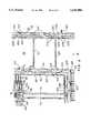
- FIG. 1is a diagrammatic top plan view of a compound stage microactuator constructed in accordance with the present invention
- FIG. 2is an enlarged partial view of the central stage and a first frame stage of the assembly of FIG. 1;
- FIG. 3is an enlarged partial view of the microactuator assembly of FIG. 1, showing portions of the central stage and x, y, and z support stage assemblies;
- FIGS. 4(a) through 4(j)illustrate in tabular form a process for fabricating the microactuator of FIG. 1 at representative cross-sections A, B, and C thereof;
- FIG. 5is a perspective enlarged view of an emitter for the central stage of the microactuator
- FIG. 6is a cross-sectional view of the emitter of FIG. 5.
- FIGS. 7(a)-7(j)illustrate in tabular form a process for fabricating a fully self-aligned gated field emitter integrated on a silicon beam
- FIGS. 8(a)-8(e)illustrate in tabular form a process for fabricating a fully self-aligned gated field emitter integrated on a released silicon beam.
- a compound stage actuator 10is fabricated from a single crystal silicon substrate 12 as a released, cantilevered structure within a cavity 14 formed in the substrate.
- the released structure 10includes a central stage portion 16 connected to a multistage support assembly 18 which holds the central stage above the floor 20 of the cavity for 6-way motion in x, y, z, roll, pitch, and yaw directions.
- This central Stage portion 16may incorporate microelectronic devices such as cathode emitters 22, capacitor plates, sensors or the like, which preferably are fabricated using the SCREAM process (to be described) or a process compatible with it, at the same time the remainder of the structure is formed.
- the multistage support assembly 18provides an interconnect system which connects external signal sources or receivers (not shown), which may be incorporated in substrate 12, to selected components, such as emitters 22, carried by the central stage portion 16 as well as to components of the support assembly for use in control or sensing operations.
- the interconnect systemuses parts of the support assembly itself as the electrically conductive elements, with suitable insulating segments being provided to define specific signal paths through the assembly. These insulating segments provide mechanical connections between various components of the structure to provide structural integrity while providing electrical isolation between adjacent parts to permit complex interconnection schemes.
- the central stage portion 16(FIG. 2) is supported mechanically within a first support frame stage 24 which includes a frame comprising a released beam 26 surrounding the stage 16 and spaced above the floor 20 of the cavity 14 in the substrate 12.
- the central stage 16is fixedly secured within this first, innermost beam, or frame 26 so that they move together.
- the frame 26is rectangular, including opposite sides 28, 30, and 32, 34 surrounding the central stage portion 16, and is coplanar therewith.
- the first support frame stage 24includes a plurality of interconnect beams 36-38 and 40-42 extending inwardly from the frame sides 28 and 30, respectively, to secure the central stage 16 in place.
- the beam 26extends circumferentially around the central stage and provides a rigid support frame which will not twist under applied forces, to thereby permit precision positioning of the central stage.
- the beam 26 forming the framepreferably is fabricated with a high aspect ratio for stiffness in the vertical direction. Although illustrated as a single beam, it will be understood that frame stage 24 may incorporate plural parallel circumferential beams, with adjacent beams being interconnected by bridges to further increase frame rigidity and to provide electrical connection between adjacent circumferential beams in the manner described below for the outer frames.
- This first support frame stage 24is mounted within a second, or intermediate support frame stage 50 which preferably is constructed of plural, parallel released beams such as beams 52-54 (FIG. 3), circumferentially surrounding and spaced from the first frame 24 and coplanar therewith.
- the second frame stage 50is preferably rectangular, with its sides, or edges 56, 58 and 60, 62 being parallel to and spaced from corresponding sides, or sides 28, 30 and 32, 34 of the first frame beam 26.
- the first frame 26is mounted to the second frame by x-axis and y-axis connectors 64 and 66, respectively, which support the first frame for motion along one axis with respect to the second frame.
- the first frame stage 24is supported for motion along an x-axis 68 passing through the center of the central stage 16.
- the y-axis connectors 66 of the second frame stage 50are in the form of elongated y-axis spring mounted beams 70, 72 and 74, 76, which are released beams extending parallel to the y-axis 78 of the device and connected at their opposite ends to corresponding edges, or sides, of the first and second frame stages 24 and 50.
- These y-axis spring mounting beamsare laterally flexible to allow the frame stage 24 to move along the x-axis with respect to frame stage 50.
- these spring mounting beamshave high aspect ratios so that they are flexible in the x direction, but are substantially inflexible in the z direction, which is perpendicular to the plane of the device, so that motion of stage frame 24 with respect to the stage frame 50 is constrained to the x-y plane of the first frame 24 along the x-axis. Motion of the central stage 16 follows that of stage 24.
- Motion of stage 24 with respect to stage 50is produced by, and may be sensed by, comb-type drive capacitors 80 and 82 having first plates 84 and 86 extending outwardly from opposite sides 32 and 34, respectively, of stage 24 and interleaved with second plates 88 and 90 extending inwardly from corresponding opposed edges 60 and 62 of the frame 50.
- the plates 84 and 88, and plates 86 and 90are interleaved so that the application of potentials across the respective drive capacitors 80 and 82 produces corresponding controlled motion in the x direction, or in the alternative, potentials across these plates can be measured to determine the location of the inner frame 24 with respect to frame 50.
- Frame stage 50is, in turn, mounted to an outermost frame stage 100 which is similar in structure to that of frame 50 and thus is comprised of plural, parallel, mechanically interconnected, released beams 102, 103, and 104 extending circumferentially around and spaced from the inner frame 50.
- the outer frame stage 100thus is concentric with the inner frames 24 and 50 and with the central stage 16, and preferably is rectangular, with sides 106, 108 and 110, 112 being parallel to corresponding sides 56, 58 and 60, 62 of the inner frame 50. Because of its interconnected multiple beam structure, the frame 100 is sufficiently rigid to resist twisting.
- the plural beamsprovide multiple electrical paths for use in interconnecting the drive capacitors and the stage microelectronics to external circuitry, as will be described.
- the inner frame 50is mounted to the outer frame 100 by means of plural, coplanar x-axis spring mounting beams 114-117 and 120-123 which are flexible in the y direction to permit relative y-axis motion between the inner and outer frames. Motion along the y-axis is produced by comb-type capacitors 126 and 128 connected between corresponding sides 56, 106 and 58, 108 of the inner and outer frames 50 and 100, respectively.
- Each drive capacitorincludes two sets of interleaved plates, one set (130 or 132) being connected to a corresponding inner frame side (56 or 58) and the other set (134 or 136) being connected to a corresponding outer frame side (106 or 108) so that the application of a potential across the capacitors produces motion of frame 50 with respect to the outer frame 100 along the y-axis.
- Frame 100is suspended within cavity 14 formed in substrate 12 by means of cantilevered, released, coplanar suspension beams 140-142 and 144-146 extending between sides 106 and 108 of frame 100 and corresponding edges 150 and 152 of the surrounding substrate.
- suspension beams 154-157 and beams 160-163extend between frame sides 110 and 112 and corresponding edges 164 and 165 of the substrate 12. These suspension beams hold the frame 100 in the x-y plane, securing it against motion along either the x or y axis.
- the outer frame 100is capable of motion in the z direction, perpendicular to the plane of the frame, toward and away from the substrate cavity floor 20. This motion may be under the control of a potential applied between a conductive layer on the floor 20 of cavity 14 and corresponding conductive beams on the movable frame stage 100, since the suspension beams 154-157 and 160-163 can flex in the vertical direction.
- all of the suspension beams connecting the frame 100 to the surrounding substratecan flex vertically to allow rotational motion of the outer frame 100 with respect to the substrate and around the z axis, which is perpendicular to the xy plane. This allows the entire actuator assembly 10 to be moved in clockwise or counterclockwise directions in the x-y plane.
- Such rotational, or yaw motioncan be produced by means of potentials applied across conductive beam segments at the corners of frame 100 and adjacent capacitive plates (indicated by dotted lines 166) on adjacent walls of cavity 14.
- suspension beamsare secured at their outer ends to corresponding connectors fabricated by a silicon on insulation (SOI) process whereby electrical connections can be made to the beams from external circuitry by way of contact pads and suitable conductors formed on the substrate.
- SOIsilicon on insulation
- suspension beams 140-142are connected to connector pads 170-172, respectively and beams 144-146 are connected to pads 174-176, respectively, through SOI connections, with each of the pads then being electrically connected by way of corresponding conductors 178-180 and 181-183 to control or sensing circuits (not shown) which may be incorporated in the substrate 12 or may be external thereto.
- the outer ends of beams 154-157 and 160-163are connected through corresponding SOI connections, pads 184-187 and 190-193 and conductors 194-197 and 200-203 to respective control or sensing circuits.
- the circumferential beams 52-54 which make up frame 50are interconnected by way of mechanically supportive bridge connectors such as those illustrated at 210.
- These bridge connectorsare fabricated integrally with the circumferential beams 52, 53, and 54 and are mechanically strong to provide a rigid frame structure, as well as to provide electrical connection between the circumferential beams.
- the circumferential beams 102-104 which make up frame 100are mechanically and electrically interconnected by bridge connectors such as those illustrated at 212, to make a rigid frame structure.
- suspension beams 140-142, 144-146, 154-157, and 160-163are mechanically connected at spaced locations to the outer frame 100, and preferably are integral therewith, to suspend the frame, and thus the entire actuator assembly 10, within cavity 14 and spaced above floor 20.
- These suspension beamsprovide electrical connections between the connector pads on the substrate and the frame 100, and are electrically connected to the outer drive plates 134, 136 of capacitors 126 and 128 or through selected inner conductor beams to the inner frames and to the central stage.
- these suspension beamsare illustrated as being single beams, it will be apparent that they can be fabricated as multiple parallel beams interconnected by bridges spaced to provide the desired rigidity or flexibility.
- the plural circumferential beams making up each of the inner and outer frames 50 and 100 and the interconnecting bridges 210 and 212 which mechanically strengthen the frames,are normally electrically conductive, and thus can be used to conduct electrical signals from exterior circuitry to selected components of the actuator assembly.
- Electrically insulating segmentssuch as segments 214 and 216 in frames 50 and 100, respectively, selectively divide the circumferential beams into plural isolated electrical segments.
- selected bridgessuch as those illustrated at 218 and 220 are also electrically insulating, and cooperate with insulating segments in the circumferential beams to define isolated electrical paths by which each of the outer conductors can be connected to a preselected component of the assembly.
- outer suspension beam 160can be connected through selected segments 222-224 and bridges 225 and 226 of frame 100, support beam 120 and segment 227 of beam 54 of frame 50 for electrical connection to the drive capacitor plates 130 on frame 50.
- outer suspension beam 142can be connected through selected segments of beams 102-104 making up the outer frame 100 and through selected bridges to capacitor plates 134 interleaved with the aforementioned plates 130.
- Another suspension beam 161can be connected to the capacitor plates 86 on frame 24, as through selected segments of frames 50 and 100 and corresponding connector beams 121 and 72, and so on.
- electrical connectionscan be made as required to activate the compound stage actuator device of the invention to move the central stage 16 in three directions. Similar connections to capacitive plates on the floor and walls of the cavity and on frame 100 can provide three directions of rotational motion.
- the central stagemay support a variety of components, including various sensors or, in one embodiment, an array 230 of field emission cathodes 22 for use in vacuum microelectronic devices and applications.
- Such emittersare electrically connected to external circuitry through the connector beams and frame segments as described above. These beams and frame segments are resistive, and thus function as series emitter resistors to limit sharp rises in current not only to protect the emitter cathodes, but to provide improved uniformity of emission where a plurality of such cathodes are provided.
- the central stage 16was capable of scanning a 20 ⁇ m ⁇ 20 ⁇ m micrometer area in the x-y plane and was capable of moving up and down ⁇ 500 nm. Further, it was capable of operating at scan rates of greater than 20 kHz.
- FIGS. 4(a)-4(j)A process for fabricating the single crystal silicon actuator 10 described above is outlined in diagrammatic tabular form in FIGS. 4(a)-4(j) which illustrate the effect of the process steps at different cross sectional regions of the actuator structure.
- Cross section Aillustrates the various electrically conductive beams or beam segments, such as the circumferential beams 52-54 and 102-104, as well as the suspension beams securing the frame 100 within cavity 14, the connector beams between frames, the bridges, the various capacitor plates, etc.
- This cross sectionmay be taken, for example, at A in FIG. 3 on beam 54.
- cross section Balso found in FIG. 3 on beam 54, illustrates the cross sectional region of beam segments which are to be completely oxidized during the process to form insulating segments.
- Cross section C at connector pad 172 in FIG. 1,is an illustration of the process for fabricating a silicon on insulator (SOI) connection between the suspension beams and connector pads formed on the substrate.
- SOIsilicon on
- the starting substrate 12is an arsenic-doped 0.005 ohm-cm, n-type, (100) silicon wafer.
- a layer 240 of silicon dioxide, preferably 500 nm thick,is thermally grown on this silicon substrate in a pyrogenic steam oxidation at 1100° C., and is used as an etch mask, identified in FIG. 4(a) as mask 1.
- the pattern for producing the released single crystal silicon structureis created using a photolithographic techniques. To obtain nanometer-scale feature sizes by this process, a contrast-enhancement material is used with KTI-OCG 895i 5cs photoresist such as the photoresist layer 242 for patterning.
- This photoresist materialis spun on the top surface of the silicon dioxide layer 240 at 6 krpm to a thickness of 0.5 micrometers.
- the desired pattern for the actuator assembly 10is then used for a photolithographic exposure of the photoresist material, defining the desired width and length of each of the components of the actuator.
- the pattern line width of the structural beamsis about 500 nm, as illustrated at cross section A, while the pattern line width for those beam segments which are to provide oxide isolating segments is about 200 nm, as illustrated at cross section B.
- the photoresist pattern 242is transferred to the silicon dioxide layer 240 in a CHF 3 /O 2 plasma etch at flow rates of 30 sccm/0.5 sccm at a chamber pressure of 30 mTor and a DC bias of -440 volts in a custom parallel plate RIE system.
- the etch rate of the silicon dioxideis 230 nm per minute.
- the photoresistis stripped by an O 2 plasma etch.
- the resulting silicon dioxide patternis transferred to the silicon substrate, in the manner illustrated in FIG. 4(b), using a Cl 2 -RIE.
- the Cl 2 etchingremoves any organic residue and native oxide on the silicon surface, and thereafter a silicon etch is performed in a Cl 2 /BCl 3 plasma etch at flow rates of 49 sccm/7 sccm at a chamber pressure of 20 mTorr and a DC bias of -400 volts.
- the depth of the silicon etch illustrated in FIG. 4(b)is 3 micrometers, leaving mesas, or islands, 244 which are to become the various beams and bridges of the actuator.
- a 310 nm thick silicon dioxide layer 240is left on top of the etched silicon lines 244.
- a sidewall silicon dioxide layer 246is thermally grown to a thickness of 250 nm in a steam O 2 ambient at 1000° C., as illustrated in FIG. 4(c).
- the width of the mesas 244are reduced due to the consumption of silicon during the oxidation step, so that the wider mesas are reduced, as indicated at 248 in cross sections A and C, and the narrower line segments (initially 200 nm wide) are fully oxidized, as illustrated at 250 in FIG. 4(c), cross section B.
- the narrower line segmentscan be placed at any desired location within the actuator to provide the desired oxidized segments for electrical insulation, these segments still being sufficiently wide to provide the required mechanical connection and strength for the structure.
- the oxidized segment 250may correspond, for example, to the segments 214, 216, 218, and 220 illustrated in FIG. 3.
- a 100 nm layer of LPCVD silicon nitride 252is conformally deposited on the silicon dioxide layer 246.
- This silicon nitride(Si 3 N 4 ) serves as an oxidation mask to protect the beam structure during subsequent oxidation steps which occur during the formation of the SOI structures.
- the demands of the structural designmay require that the beam width be greater than that which will permit complete oxidation during the steps illustrated at FIG. 4(c), yet complete oxidation is required for isolation at that location.
- the isolation process described aboveis followed by a selective oxidation step before the SOI structure is formed.
- a dielectric stack of nitride/oxide(100 nm/100 nm) is deposited by LPCVD and PECVD.
- the nitride on the top and upper part of the sidewalls of the silicon segments which are to be oxidizedis selectively stripped, using an oxide etch mask, by hot (160° C.) phosphoric acid solution to provide an oxidation window opening which allows the silicon segments to be fully oxidized, while the structural base-silicon is not oxidized. This is followed by a second thermal oxidation to completely oxidize the selected segments, and a conformal layer of silicon nitride is provided to cover the window.
- a photoresist layer 254is spun on the silicon nitride layer 252, for example, at 2.50 krpm in 60 seconds to a thickness of 3.5 micrometers, as illustrated in FIG. 4(d), cross sections A and B.
- a second maskis then used to pattern the desired SOI structures in the photoresist material, this pattern being generally indicated at 256 in FIG. 4(d), cross section C, taken at the edge 150 of substrate 12, as illustrated in FIG. 1.
- This SOI structureis used to mechanically connect a beam to the substrate and to provide an electrical connection between the beam (such as beam 142 in FIG.
- the pattern 256 of the SOI structuresdefines each of the connectors at the outer ends of suspension beams 140-142, 144-146, 154-157, and 160-163.
- the nitride/oxide exposed by the patternis vertically etched back with CHF 3 /O 2 plasma etch, again as illustrated at cross section C in FIG. 4(d).
- the vertical etchremoves the dielectric stack on horizontal surfaces, for example at the base of the mesa 244 (cross section C) while leaving at least some of the silicon dioxide mask 240 on the top of mesa 244 and the silicon dioxide 246 on its sidewalls, while also leaving the silicon nitride 252 on the sidewalls.
- the next step in the processis an isotropic silicon recess etch, illustrated at FIG. 4(e), which is performed using a fluorinated silicon (SF 6 ) RIE.
- This recess etchillustrated at 258 (in FIG. 4(e), cross section C) removes silicon from the top layer of substrate 12 and etches under the edges of the sidewall nitrate 252 to produce the undercut region 258.
- This recess etchenhances the lateral oxidation at the base of the silicon line 244 during the subsequent oxidation step by increasing the transport of oxidizing species underneath the single crystal silicon line.
- This recess etchhas no effect at cross sections A and B.
- the photoresist layer 254 which had been used to protect the beam structuresis then stripped by an O 2 plasma etch, as illustrated in FIG. 4(f) and an 1100° C. pyrogenic steam oxidation is performed to grow a 700 nm thick field oxide 260 which laterally undercuts the single crystal silicon line 244 at cross section C, thereby producing the isolated beam segment 262 (FIG. 4(f) at cross section C), which beam section may be a part, for example, of suspension beam 142 in FIG. 1.
- the single crystal silicon lines 248 and 250 at cross sections A and Bare protected from the oxidation step by the silicon nitride layer 252.
- metal-contact windowsare opened on the top of the single crystal silicon lines, where required, and over corresponding contact pads previously formed in the surrounding silicon wafer 12.
- Such contact pads in the wafermay have been fabricated during the formation of electrical circuits on the surface of the wafer, the pads being covered by a layer of oxide prior to formation of the actuator 10.
- such padsmay be exposed by the window mask (Mask 3) formed by conventional photolithography in a photoresist layer 264.
- the photoresist on top of the beam 262is exposed through its complete thickness, while the resist material to the sides of the beam region is sufficiently thick to prevent exposure completely through the photoresist.
- the exposed photoresistis completely developed away on top of beam 262, as at region 266 (FIG. 4(g), cross section C) so that the silicon dioxide layers 240 and 260 on top of the silicon beam 262 are etched using CHF 3 /O 2 plasma etch to reveal the top surface 268 of beam 262.
- the contact pad for this beammay also be opened, after which the photoresist 264 is stripped away using an O 2 plasma etch. Thereafter, the silicon nitride layer 252 is stripped, using hot phosphoric acid at 160° C., as illustrated in FIG. 4(h).
- Metallization of the metal contact windowis completed by an aluminum lift off using a tri-layer resist process.
- a 300 nm layer of aluminumis applied, using mask 4 (FIG. 4(i)), the aluminum layer 270 conformally covering the SOI structure 262.
- a DC magnitron sputter deposition processmay be used to provide the layer 270 (cross section C).
- a metal etch stepis then used to remove excess metal.
- the silicon dioxide 246 on the horizontal surface of substrate 12 at the base of the lines 248 and 250is then removed by a second etch back using CHF 3 /O 2 plasma etch.
- the thicker field silicon dioxideremains on the top surface of the lines 248 and on the sidewalls thereof, while the aluminum layer 270 protects the oxide layer 260 beneath the beam 262 (cross section C).
- the lines 248 and 250are completely released from the silicon substrate 12 using an SF 6 RIE process in the same etch conditions as were used in the silicon recess etch, thereby providing released beam 248 and released beam 250, illustrated in FIG. 4(j) at cross sections A and B. It is noted that the beam 248 is protected by the silicon dioxide layer 246 during this last release step.
- the beam 248thus corresponds to the silicon beams utilized in the actuator assembly 10, as discussed above.
- the silicon dioxide layer 260 for the SOI structureis not etched, leaving the SOI structure clamping the ends of the beams to the substrate.
- released silicon beamssuch as the beams 248 illustrated at cross section A in FIG. 4(j) can incorporate one or more field emission cathodes, such as the cathode 22 illustrated in FIG. 2.
- a single such cathodeis illustrated in FIG. 5 at 280, this cathode being formed on a beam 282 which may, for example, be one of the beams forming a part of central stage 16 and illustrated in FIG. 2.
- FIGS. 7(a) to 7(j)illustrate a process for building a gated field emitter on a high aspect ratio silicon structure with submicron lateral feature size.
- the silicon base for the emittercan be released or unreleased; in the illustrated embodiment of FIGS. (7a)-7(j) the base is unreleased, but the process can be combined with that described above for actuator 10 to provide emitters on released beams, as will be described below.
- a 350 nm thick layer 284 of P(MMA-MAA) (9%) copolymer resist on a substrate 286 and dielectric layer 288 and 289is electron-beam exposed in a Cambridge Instruments EBMF-10.5/CS system at 20 kV beam energy and 1.5 nA beam current on a 1.6384 mm exposure field (see FIG. 7(a)).
- the tipis defined by a 500 ⁇ 500 nm 2 island 290 surrounded by a 150 nm wide trench 292.
- the pattern in the developed electron-beam resistis transferred to underlying dielectric films of plasma enhanced chemical vapor disposition (PECVD) oxide 288 (100 nm) and low pressure chemical vapor deposition (LPCVD) nitride 289 (100 nm) using CHF 3 /O 2 RIE, and then to the substrate-silicon 286 using SF 6 RIE (see FIG. 7(b)).
- PECVDplasma enhanced chemical vapor disposition
- LPCVDlow pressure chemical vapor deposition
- nitride 289100 nm
- the silicon etchproduces a 1 ⁇ m deep trench 294 with 200 nm lateral undercut under the oxide film 288, which is used as an etch mask, and produces a central island 295.
- a 100 nm thick oxide layer 296thermally grows on the exposed silicon (see FIG. 7(c)).
- the nitride film 289 that remains from the previous silicon etch stepserves as an oxidation mask.
- This oxidation stepprovides an oxide layer which reduces the size of island 295 as well as the sidewalls 300 and bottom 302 of the silicon trench to produce silicon tip 304, which is sharpened and, thereby, has a thicker oxide covering on the tip apex due to the isotropic reduction of the dimensions by consumption of some of the surface silicon.
- a planarization processis used to completely fill the silicon trench 294 (see FIG. 7(d)) with oxide 306.
- the planarization processis performed with alternative deposition and vertical etchback of PECVD oxide and planarizing material (KTI-OCG photoresist), and is finished by removing the dielectric stack, including nitride 289, covering over the substrate-silicon.
- the oxide 306 in the trench and covering over the silicon tipis used for a subsequent silicon etch mask to redefine the silicon emitter base-structures.
- a silicon structural beam having a width of 800 nm to support tip 304is required by the 300 nm trench patterning and the tip etch and oxidation described above.
- silicon 286is vertically etched back past the level of the trench bottom 302, and then down 3 ⁇ m to form the beam structure 310 by a Cl 2 /BCl 3 RIE etch (see FIG. 7(e)).
- the oxide etch mask 306is stripped off using buffered hydrofluoric acid solution.
- a 250 nm thick oxide film 312is provided to conformally cover beam 310 and tip 304 by depositing PECVD oxide (see FIG. 7(f)).
- the following gate-electrode metallizationis performed on the oxide film with a conformal, rather than a level, coating.
- a sputtered Ti 0 .1 W 0 .9 film 314is deposited on the oxide film (see FIG. 7(g)).
- a 3.5 ⁇ m thick planarizing material 316(KTI-OCG 895i 50cs photoresist) is spun on the Ti 0 .1 W 0 .9 film, the thickness of the photoresist corresponding to the 3 ⁇ m height of the structure 310, 304 (see FIG. 7(h)).
- the photoresist directly above the tip apexis thinner than over the remainder of the surface.
- An O 2 plasma etchbackexposes the Ti 0 .1 W 0 .9 layer 314 above the apex, at 318.
- the exposed Ti 0 .1 W 0 .9is then etched using an SF 6 RIE, most of the Ti 0 .1 W 0 .9 lying underneath the photoresist being protected by the photoresist (see FIG. 7(i)), as indicated at 320. This etch does not affect the oxide.
- the oxide 312 covering the tipis then removed using buffered hydrofluoric acid solution.
- the remaining photoresist 316is stripped off (see FIG. 7(j)), leaving the metal layer 314 surrounding the tip 304 and providing a gate electrode aperture 322 for the tip.
- the electrodepreferably has a gate aperture diameter of about 500 nm, but the diameter of aperture 322 can range from 200 to 800 nm.
- the aperture diameteris determined, in part, by the thickness of the conformal oxide film 312.
- the emitter fabrication process described abovecan be used separately, it can also be fully integrated into the microelectromechanical actuator 10 of the present invention, to provide, for example, emitters on submicrometer wide beams in the center stage portion 16.
- the integrated processstarts with the arsenic-doped, 0.005 ⁇ cm, n-type, (100) silicon substrate 12 (or 286, as shown in FIG. 7(a)) on which there are 100 nm thick films of nitride 289 and oxide 288 deposited.
- the first stage in forming the silicon structuresis to produce the 1 ⁇ m height silicon tips by producing 1 ⁇ m deep trenches 294, as shown in FIG. 7(b), as by electron-beam lithography and oxide/nitride etch and silicon etch.
- the trench widthsrange from 150 to 250 nm.
- 150 nm wide trenchescan also be provided where desired to form 300 nm wide, suspended oxide segments (such as segment 250 in FIGS.
- a 100 nm film 296 of thermal oxidecovers the tips and the bottom and sidewalls of the trenches by an oxidation step.
- the thermal oxidation stepfurther sharpens the tips and provides thicker oxide on the apexes.
- a planarization processis performed to fill PECVD oxide in the trenches.
- the second stage of the integrated processis forming high aspect-ration silicon structures, either with or without emitters.
- the entire actuator structureis defined by the pattern in the oxide filling in the trenches and covering over the tips in FIG. 7(d) and covering the substrate in FIG. 4(a) (cross sections A, B, and C).
- a Cl 2 /BCl 3 RIEis performed to etch silicon 3 ⁇ m deep using the oxide as an etch mask.
- the integrated processcontinues with isolation and metallization processes as shown in FIGS. 4(d) to 4(j) to produce the composite XYZ stages with the integrated electro-mechanical sensors and actuators.
- the suspended silicon structural beams for the emittersare 800 nm wide and 3 ⁇ m thick, and are coated by conformal oxide film.
- the oxide 246 and 306 on the portion of the structures with integral silicon tipsis etched away and a new conformal oxide 330 is deposited (see FIG. 8(b)).
- the metallization process of the integrated emitter gatesis performed, as outlined in FIGS. 7(g)-7(j), except that it is performed on a released beam 310.
- the pattern of the gate electrodesis created using trilayer resist, photolithography and metal (e.g. sputter Ti 0 .1 W 0 .9) liftoff.
- the trilayer resistconsists of 4 ⁇ m photoresist (KTI-OCG), 100 nm PECVD oxide (deposited at 90° C.) and 500 nm photoresist.
- the pattern in the developed photoresistis transferred into the oxide by CHF 3 /O 2 RIE, and then into the base photoresist 332 by O 2 RIE.
- the base photoresistis etched by O 2 RIE until most of the vertical sidewalls 334 of the released structure 310 is exposed (see FIG. 8(c)). After the metal 314 is deposited on the oxide/photoresist stack the excess is "lifted off" by using acetone to dissolve the photoresist.
- Windows for gate aperture openingsare defined in redeposited trilayer resist by photolithography and RIE etches of oxide and base photoresist.
- the O 2 RIE etchis stopped once the gate metal above the tip apexes is exposed (see FIG. 8(d)), the metal is etched, and the oxide covering over the silicon tips and the remaining base photoresist are removed by buffered hydrofluoric acid solution and O 2 RIE, respectively (see FIG. 8(e)), to provide a gate aperture surrounding a tip on a released beam.
- such a released beam 282may incorporate a silicon core 310, similar to the beam in FIG. 8(e), which is released from the floor 20 of substrate 12 in the manner described above.
- Core 310is covered by a silicon dioxide layer 330 and may incorporate, for example, one or more oxide segments 250 which electrically insulate regions of the beam 282, such as region 340 from adjacent regions of that beam, such as region 342.
- An oxide conformal layer 330is provided on the surface of core 310 in the region of the emitter 280, to insulate the metal gate electrode layer from the silicon core.
- the metal gate electrode 314contacts the silicon core 310 in regions 340 through a window 344 formed in oxide layer 286, while the emitter tip 304 is connected by way of beam portion 342 and window 346 to metal layer 270 (see FIG. 4(j), Section C) at the substrate to which the beam 282 is connected.
- the substrateis the center stage 16 of the actuator, through which electrical connections are made through conductive paths in the actuator beam structure.
- beam section 340can be connected to an SOI section at the opposite side of stage 16 (see FIG. 2).
Landscapes
- Engineering & Computer Science (AREA)
- Microelectronics & Electronic Packaging (AREA)
- Chemical & Material Sciences (AREA)
- Computer Hardware Design (AREA)
- Manufacturing & Machinery (AREA)
- Analytical Chemistry (AREA)
- Nanotechnology (AREA)
- Health & Medical Sciences (AREA)
- Crystallography & Structural Chemistry (AREA)
- Molecular Biology (AREA)
- General Health & Medical Sciences (AREA)
- Life Sciences & Earth Sciences (AREA)
- Micromachines (AREA)
Abstract
Description
Claims (40)
Priority Applications (3)
| Application Number | Priority Date | Filing Date | Title |
|---|---|---|---|
| US08/069,725US5536988A (en) | 1993-06-01 | 1993-06-01 | Compound stage MEM actuator suspended for multidimensional motion |
| US08/443,331US5506175A (en) | 1993-06-01 | 1995-05-17 | Method of forming compound stage MEM actuator suspended for multidimensional motion |
| US08/588,919US5726073A (en) | 1993-06-01 | 1996-01-19 | Compound stage MEM actuator suspended for multidimensional motion |
Applications Claiming Priority (1)
| Application Number | Priority Date | Filing Date | Title |
|---|---|---|---|
| US08/069,725US5536988A (en) | 1993-06-01 | 1993-06-01 | Compound stage MEM actuator suspended for multidimensional motion |
Related Child Applications (1)
| Application Number | Title | Priority Date | Filing Date |
|---|---|---|---|
| US08/443,331DivisionUS5506175A (en) | 1993-06-01 | 1995-05-17 | Method of forming compound stage MEM actuator suspended for multidimensional motion |
Publications (1)
| Publication Number | Publication Date |
|---|---|
| US5536988Atrue US5536988A (en) | 1996-07-16 |
Family
ID=22090824
Family Applications (3)
| Application Number | Title | Priority Date | Filing Date |
|---|---|---|---|
| US08/069,725Expired - LifetimeUS5536988A (en) | 1993-06-01 | 1993-06-01 | Compound stage MEM actuator suspended for multidimensional motion |
| US08/443,331Expired - LifetimeUS5506175A (en) | 1993-06-01 | 1995-05-17 | Method of forming compound stage MEM actuator suspended for multidimensional motion |
| US08/588,919Expired - LifetimeUS5726073A (en) | 1993-06-01 | 1996-01-19 | Compound stage MEM actuator suspended for multidimensional motion |
Family Applications After (2)
| Application Number | Title | Priority Date | Filing Date |
|---|---|---|---|
| US08/443,331Expired - LifetimeUS5506175A (en) | 1993-06-01 | 1995-05-17 | Method of forming compound stage MEM actuator suspended for multidimensional motion |
| US08/588,919Expired - LifetimeUS5726073A (en) | 1993-06-01 | 1996-01-19 | Compound stage MEM actuator suspended for multidimensional motion |
Country Status (1)
| Country | Link |
|---|---|
| US (3) | US5536988A (en) |
Cited By (103)
| Publication number | Priority date | Publication date | Assignee | Title |
|---|---|---|---|---|
| US5708319A (en)* | 1995-03-23 | 1998-01-13 | Kabushiki Kaisha Toyoda Jidoshokki Seisakusho | Multiple axes drive apparatus with electrostatic drive means |
| US5723916A (en)* | 1996-05-17 | 1998-03-03 | Delco Electronics Corporation | Electrical load driving device including load current limiting circuitry |
| US5786621A (en)* | 1995-06-23 | 1998-07-28 | Cornell Research Foundation, Inc. | Microelectromechanical integrated microloading device |
| US5801472A (en)* | 1995-08-18 | 1998-09-01 | Hitchi, Ltd. | Micro-fabricated device with integrated electrostatic actuator |
| US5844251A (en)* | 1994-01-05 | 1998-12-01 | Cornell Research Foundation, Inc. | High aspect ratio probes with self-aligned control electrodes |
| WO1999024783A1 (en)* | 1997-11-06 | 1999-05-20 | Mcnc | Microelectromechanical positioning apparatus |
| WO1999012002A3 (en)* | 1997-09-02 | 1999-08-05 | Analog Devices Inc | Micromachined gyros |
| US5949342A (en)* | 1997-12-31 | 1999-09-07 | Storage Technology Corporation | Shock sensing and reporting device |
| US5955817A (en)* | 1996-12-16 | 1999-09-21 | Mcnc | Thermal arched beam microelectromechanical switching array |
| US5963367A (en)* | 1997-09-23 | 1999-10-05 | Lucent Technologies, Inc. | Micromechanical xyz stage for use with optical elements |
| US6054335A (en)* | 1997-12-12 | 2000-04-25 | Xerox Corporation | Fabrication of scanning III-V compound light emitters integrated with Si-based actuators |
| US6084257A (en)* | 1995-05-24 | 2000-07-04 | Lucas Novasensor | Single crystal silicon sensor with high aspect ratio and curvilinear structures |
| US6091537A (en)* | 1998-12-11 | 2000-07-18 | Xerox Corporation | Electro-actuated microlens assemblies |
| US6116756A (en)* | 1997-12-12 | 2000-09-12 | Xerox Corporation | Monolithic scanning light emitting devices |
| US6133670A (en)* | 1999-06-24 | 2000-10-17 | Sandia Corporation | Compact electrostatic comb actuator |
| US6137206A (en)* | 1999-03-23 | 2000-10-24 | Cronos Integrated Microsystems, Inc. | Microelectromechanical rotary structures |
| US6180428B1 (en) | 1997-12-12 | 2001-01-30 | Xerox Corporation | Monolithic scanning light emitting devices using micromachining |
| US6211598B1 (en) | 1999-09-13 | 2001-04-03 | Jds Uniphase Inc. | In-plane MEMS thermal actuator and associated fabrication methods |
| US6218762B1 (en) | 1999-05-03 | 2001-04-17 | Mcnc | Multi-dimensional scalable displacement enabled microelectromechanical actuator structures and arrays |
| US6236139B1 (en) | 1999-02-26 | 2001-05-22 | Jds Uniphase Inc. | Temperature compensated microelectromechanical structures and related methods |
| US6239473B1 (en) | 1998-01-15 | 2001-05-29 | Kionix, Inc. | Trench isolation for micromechanical devices |
| US6253011B1 (en) | 1998-12-30 | 2001-06-26 | Mcdonnell Douglas Corporation | Micro-aligner for precisely aligning an optical fiber and an associated fabrication method |
| US6255757B1 (en) | 1999-09-01 | 2001-07-03 | Jds Uniphase Inc. | Microactuators including a metal layer on distal portions of an arched beam |
| US6275320B1 (en) | 1999-09-27 | 2001-08-14 | Jds Uniphase, Inc. | MEMS variable optical attenuator |
| US6291922B1 (en) | 1999-08-25 | 2001-09-18 | Jds Uniphase, Inc. | Microelectromechanical device having single crystalline components and metallic components |
| US6308631B1 (en) | 2000-07-20 | 2001-10-30 | The United States Of America As Represented By The Secretary Of The Navy | Mems vertical to horizontal motion translation device |
| US6316796B1 (en) | 1995-05-24 | 2001-11-13 | Lucas Novasensor | Single crystal silicon sensor with high aspect ratio and curvilinear structures |
| US20020021055A1 (en)* | 2000-08-18 | 2002-02-21 | Lee Jin-Ho | Micro-actuator and manufacturing method thereof |
| WO2002017470A1 (en)* | 2000-08-25 | 2002-02-28 | Iolon, Inc. | Micromechanical device having two degrees of motion |
| EP1184888A1 (en)* | 2000-08-30 | 2002-03-06 | Agere Systems Guardian Corporation | On-chip vacuum tube device and process for making the device |
| WO2001057902A3 (en)* | 2000-02-03 | 2002-03-14 | Calient Networks Inc | Electrostatic actuator for microelectromechanical systems and methods of fabrication |
| US6359757B1 (en) | 1999-06-02 | 2002-03-19 | Maxtor Corporation | Electrostatic actuator |
| US6366340B1 (en)* | 1995-08-18 | 2002-04-02 | Hitachi, Ltd. | Electron exposure apparatus |
| US6373682B1 (en) | 1999-12-15 | 2002-04-16 | Mcnc | Electrostatically controlled variable capacitor |
| US6377438B1 (en) | 2000-10-23 | 2002-04-23 | Mcnc | Hybrid microelectromechanical system tunable capacitor and associated fabrication methods |
| US6396620B1 (en) | 2000-10-30 | 2002-05-28 | Mcnc | Electrostatically actuated electromagnetic radiation shutter |
| US6438954B1 (en) | 2001-04-27 | 2002-08-27 | 3M Innovative Properties Company | Multi-directional thermal actuator |
| US6445107B1 (en) | 2000-07-18 | 2002-09-03 | Samsung Electronics Co., Ltd. | Single stage microactuator for multi-dimensional actuation |
| US6449098B1 (en) | 2000-05-16 | 2002-09-10 | Calient Networks, Inc. | High uniformity lens arrays having lens correction and methods for fabricating the same |
| US20020127760A1 (en)* | 2000-08-02 | 2002-09-12 | Jer-Liang Yeh | Method and apparatus for micro electro-mechanical systems and their manufacture |
| US6456420B1 (en) | 2000-07-27 | 2002-09-24 | Mcnc | Microelectromechanical elevating structures |
| US6483419B1 (en) | 2000-09-12 | 2002-11-19 | 3M Innovative Properties Company | Combination horizontal and vertical thermal actuator |
| US6483961B1 (en) | 2000-06-02 | 2002-11-19 | Calient Networks, Inc. | Dual refraction index collimator for an optical switch |
| US20020172136A1 (en)* | 2001-05-17 | 2002-11-21 | Fujitsu Limited | Optical disk apparatus with electrostatic lens actuator |
| US6485273B1 (en) | 2000-09-01 | 2002-11-26 | Mcnc | Distributed MEMS electrostatic pumping devices |
| US6507138B1 (en) | 1999-06-24 | 2003-01-14 | Sandia Corporation | Very compact, high-stability electrostatic actuator featuring contact-free self-limiting displacement |
| US6509670B2 (en) | 2000-07-19 | 2003-01-21 | Samsung Electronics Co., Ltd. | Single stage microactuator for multidimensional actuation with multi-folded spring |
| US6531668B1 (en)* | 2001-08-30 | 2003-03-11 | Intel Corporation | High-speed MEMS switch with high-resonance-frequency beam |
| US6531947B1 (en) | 2000-09-12 | 2003-03-11 | 3M Innovative Properties Company | Direct acting vertical thermal actuator with controlled bending |
| US20030062332A1 (en)* | 2001-09-28 | 2003-04-03 | Harris Richard D. | Method for fabricating a microelectromechanical system (MEMS) device using a pre-patterned bridge |
| US6544863B1 (en) | 2001-08-21 | 2003-04-08 | Calient Networks, Inc. | Method of fabricating semiconductor wafers having multiple height subsurface layers |
| US6563106B1 (en) | 2000-02-01 | 2003-05-13 | Calient Networks, Inc. | Micro-electro-mechanical-system (MEMS) mirror device and methods for fabricating the same |
| US6567448B1 (en) | 1997-12-12 | 2003-05-20 | Xerox Corporation | Scanning III-V compound light emitters integrated with Si-based actuators |
| US6590313B2 (en) | 1999-02-26 | 2003-07-08 | Memscap S.A. | MEMS microactuators located in interior regions of frames having openings therein and methods of operating same |
| US6590267B1 (en) | 2000-09-14 | 2003-07-08 | Mcnc | Microelectromechanical flexible membrane electrostatic valve device and related fabrication methods |
| US6597825B1 (en) | 2001-10-30 | 2003-07-22 | Calient Networks, Inc. | Optical tap for an optical switch |
| US6628041B2 (en) | 2000-05-16 | 2003-09-30 | Calient Networks, Inc. | Micro-electro-mechanical-system (MEMS) mirror device having large angle out of plane motion using shaped combed finger actuators and method for fabricating the same |
| US6636339B2 (en) | 2000-11-03 | 2003-10-21 | Samsung Electronics Co., Ltd. | Optical scanner, laser image projector adopting the optical scanner, and method of driving the laser image projector |
| US6643425B1 (en) | 2000-08-17 | 2003-11-04 | Calient Networks, Inc. | Optical switch having switch mirror arrays controlled by scanning beams |
| US6653239B2 (en)* | 1999-07-30 | 2003-11-25 | Xactix, Inc. | Thermal isolation using vertical structures |
| WO2002067293A3 (en)* | 2001-02-20 | 2003-11-27 | Rockwell Automation Tech Inc | Microelectromechanical systems (mems) device including an analog or a digital |
| US6664786B2 (en) | 2001-07-30 | 2003-12-16 | Rockwell Automation Technologies, Inc. | Magnetic field sensor using microelectromechanical system |
| US6668108B1 (en) | 2000-06-02 | 2003-12-23 | Calient Networks, Inc. | Optical cross-connect switch with integrated optical signal tap |
| US6690178B2 (en) | 2001-10-26 | 2004-02-10 | Rockwell Automation Technologies, Inc. | On-board microelectromechanical system (MEMS) sensing device for power semiconductors |
| US6708491B1 (en) | 2000-09-12 | 2004-03-23 | 3M Innovative Properties Company | Direct acting vertical thermal actuator |
| US6756310B2 (en) | 2001-09-26 | 2004-06-29 | Rockwell Automation Technologies, Inc. | Method for constructing an isolate microelectromechanical system (MEMS) device using surface fabrication techniques |
| US6761829B2 (en) | 2001-04-26 | 2004-07-13 | Rockwell Automation Technologies, Inc. | Method for fabricating an isolated microelectromechanical system (MEMS) device using an internal void |
| US6768628B2 (en) | 2001-04-26 | 2004-07-27 | Rockwell Automation Technologies, Inc. | Method for fabricating an isolated microelectromechanical system (MEMS) device incorporating a wafer level cap |
| US20040147056A1 (en)* | 2003-01-29 | 2004-07-29 | Mckinnell James C. | Micro-fabricated device and method of making |
| US6798312B1 (en) | 1999-09-21 | 2004-09-28 | Rockwell Automation Technologies, Inc. | Microelectromechanical system (MEMS) analog electrical isolator |
| US6798315B2 (en) | 2001-12-04 | 2004-09-28 | Mayo Foundation For Medical Education And Research | Lateral motion MEMS Switch |
| US20040189142A1 (en)* | 2003-03-25 | 2004-09-30 | Knieser Michael J. | Microelectromechanical isolating circuit |
| US20040198063A1 (en)* | 2002-06-27 | 2004-10-07 | Kanakasabapathi Subramanian | Three dimensional high aspect ratio micromachining |
| US6803755B2 (en) | 1999-09-21 | 2004-10-12 | Rockwell Automation Technologies, Inc. | Microelectromechanical system (MEMS) with improved beam suspension |
| US6815243B2 (en) | 2001-04-26 | 2004-11-09 | Rockwell Automation Technologies, Inc. | Method of fabricating a microelectromechanical system (MEMS) device using a pre-patterned substrate |
| US6825967B1 (en) | 2000-09-29 | 2004-11-30 | Calient Networks, Inc. | Shaped electrodes for micro-electro-mechanical-system (MEMS) devices to improve actuator performance and methods for fabricating the same |
| US20040252595A1 (en)* | 2003-06-13 | 2004-12-16 | Alps Electric Co., Ltd. | High precision positioning apparatus |
| US20040257380A1 (en)* | 2003-06-20 | 2004-12-23 | Herbert Leslie B. | Imaging method and system |
| US6848328B2 (en)* | 2001-03-09 | 2005-02-01 | Klocke Nanotechnik | Positioning unit and positioning apparatus with at least two positioning units |
| US20050040919A1 (en)* | 2003-08-22 | 2005-02-24 | Samsung Electronics Co., Ltd. | Two-axis actuator with large stage |
| US6887732B2 (en) | 2001-05-07 | 2005-05-03 | Applied Materials, Inc. | Microstructure devices, methods of forming a microstructure device and a method of forming a MEMS device |
| US20050172717A1 (en)* | 2004-02-06 | 2005-08-11 | General Electric Company | Micromechanical device with thinned cantilever structure and related methods |
| US20050205949A1 (en)* | 2004-03-18 | 2005-09-22 | Denso Corporation | Semiconductor device having moving part |
| US20060016486A1 (en)* | 2004-07-23 | 2006-01-26 | Teach William O | Microvalve assemblies and related structures and related methods |
| US7055437B1 (en)* | 2003-04-08 | 2006-06-06 | The United States Of America As Represented By The Secretary Of The Army | Micro-scale firetrain for ultra-miniature electro-mechanical safety and arming device |
| US7069861B1 (en)* | 2003-04-08 | 2006-07-04 | The United States Of America As Represented By The Secretary Of The Army | Micro-scale firetrain for ultra-miniature electro-mechanical safety and arming device |
| US20080042260A1 (en)* | 2006-08-21 | 2008-02-21 | Jeong Heewon | Micro-electromechanical systems device and manufacturing method thereof |
| US20080297289A1 (en)* | 2007-05-31 | 2008-12-04 | Seagate Technology Llc | Simultaneous Rotational Control Using Offset Linear Actuators |
| US7728339B1 (en) | 2002-05-03 | 2010-06-01 | Calient Networks, Inc. | Boundary isolation for microelectromechanical devices |
| US20110030472A1 (en)* | 2009-05-27 | 2011-02-10 | King Abdullah University of Science ang Technology | Mems mass-spring-damper systems using an out-of-plane suspension scheme |
| US20110216976A1 (en)* | 2010-03-05 | 2011-09-08 | Microsoft Corporation | Updating Image Segmentation Following User Input |
| US20110254404A1 (en)* | 2008-10-20 | 2011-10-20 | Robert Bosch Gmbh | Electrostatic drive, micromechanical component, and manufacturing method for an electrostatic drive and a micromechanical component |
| US20150048903A1 (en)* | 2013-08-19 | 2015-02-19 | Harris Corporation | Microelectromechanical system with a micro-scale spring suspension system and methods for making the same |
| US9093975B2 (en) | 2013-08-19 | 2015-07-28 | Harris Corporation | Microelectromechanical systems comprising differential inductors and methods for making the same |
| US9123493B2 (en) | 2014-01-23 | 2015-09-01 | Harris Corporation | Microelectromechanical switches for steering of RF signals |
| US9172352B2 (en) | 2013-08-19 | 2015-10-27 | Harris Corporation | Integrated microelectromechanical system devices and methods for making the same |
| US20150341534A1 (en)* | 2014-05-06 | 2015-11-26 | Mems Drive, Inc. | Electrical bar latching for low stiffness flexure mems actuator |
| US20160227117A1 (en)* | 2014-04-04 | 2016-08-04 | Mems Start, Llc | Actuator for moving an optoelectronic device |
| WO2017079298A1 (en)* | 2015-11-05 | 2017-05-11 | Mems Drive Inc. | Mems actuator package architecture |
| US20170268698A1 (en)* | 2016-03-15 | 2017-09-21 | Dunan Microstaq, Inc. | Mems based solenoid valve |
| US10071903B2 (en) | 2014-05-06 | 2018-09-11 | Mems Drive, Inc. | Low stiffness flexure |
| US10145739B2 (en) | 2014-04-03 | 2018-12-04 | Oto Photonics Inc. | Waveguide sheet, fabrication method thereof and spectrometer using the same |
| US12103843B2 (en) | 2021-01-20 | 2024-10-01 | Calient.Ai Inc. | MEMS mirror arrays with reduced crosstalk |
Families Citing this family (49)
| Publication number | Priority date | Publication date | Assignee | Title |
|---|---|---|---|---|
| US5536988A (en)* | 1993-06-01 | 1996-07-16 | Cornell Research Foundation, Inc. | Compound stage MEM actuator suspended for multidimensional motion |
| FR2736654B1 (en)* | 1995-07-13 | 1997-08-22 | Commissariat Energie Atomique | METHOD FOR MANUFACTURING RIGID FLOATING MICROSTRUCTURE ELEMENTS AND DEVICE EQUIPPED WITH SUCH ELEMENTS |
| US6121552A (en)* | 1997-06-13 | 2000-09-19 | The Regents Of The University Of Caliofornia | Microfabricated high aspect ratio device with an electrical isolation trench |
| KR100300193B1 (en)* | 1997-09-05 | 2001-10-27 | 하제준 | Method for manufacturing field emission array on silicon formed on insulating layer |
| US6074890A (en)* | 1998-01-08 | 2000-06-13 | Rockwell Science Center, Llc | Method of fabricating suspended single crystal silicon micro electro mechanical system (MEMS) devices |
| US6756247B1 (en) | 1998-01-15 | 2004-06-29 | Timothy J. Davis | Integrated large area microstructures and micromechanical devices |
| US6291875B1 (en) | 1998-06-24 | 2001-09-18 | Analog Devices Imi, Inc. | Microfabricated structures with electrical isolation and interconnections |
| US6433401B1 (en) | 1999-04-06 | 2002-08-13 | Analog Devices Imi, Inc. | Microfabricated structures with trench-isolation using bonded-substrates and cavities |
| AU4343800A (en) | 1999-04-15 | 2000-11-02 | Corning Incorporated | Electrothermally actuated vibromotor |
| US6703679B1 (en) | 1999-08-31 | 2004-03-09 | Analog Devices, Imi, Inc. | Low-resistivity microelectromechanical structures with co-fabricated integrated circuit |
| US6429034B1 (en) | 1999-12-16 | 2002-08-06 | Corning Incorporated | Method of making high aspect ratio features during surface micromachining |
| US6868726B2 (en)* | 2000-01-20 | 2005-03-22 | Analog Devices Imi, Inc. | Position sensing with improved linearity |
| US6440766B1 (en) | 2000-02-16 | 2002-08-27 | Analog Devices Imi, Inc. | Microfabrication using germanium-based release masks |
| EP1128540A1 (en)* | 2000-02-23 | 2001-08-29 | STMicroelectronics S.r.l. | Structure for electrically connecting microelectromechanical devices,in particular microactuators for hard disk drives |
| US6593677B2 (en) | 2000-03-24 | 2003-07-15 | Onix Microsystems, Inc. | Biased rotatable combdrive devices and methods |
| AU2001250989A1 (en)* | 2000-03-24 | 2001-10-08 | Onix Microsystems, Inc. | Two-dimensional gimbaled scanning actuator with vertical electrostatic comb-drive for actuation and/or sensing |
| US20010040419A1 (en) | 2000-03-24 | 2001-11-15 | Behrang Behin | Biased rotatable combdrive sensor methods |
| US6330102B1 (en)* | 2000-03-24 | 2001-12-11 | Onix Microsystems | Apparatus and method for 2-dimensional steered-beam NxM optical switch using single-axis mirror arrays and relay optics |
| US6612029B2 (en)* | 2000-03-24 | 2003-09-02 | Onix Microsystems | Multi-layer, self-aligned vertical combdrive electrostatic actuators and fabrication methods |
| US6585383B2 (en) | 2000-05-18 | 2003-07-01 | Calient Networks, Inc. | Micromachined apparatus for improved reflection of light |
| US6560384B1 (en) | 2000-06-01 | 2003-05-06 | Calient Networks, Inc. | Optical switch having mirrors arranged to accommodate freedom of movement |
| US6364460B1 (en) | 2000-06-13 | 2002-04-02 | Chad R. Sager | Liquid delivery system |
| US6586889B1 (en)* | 2000-06-21 | 2003-07-01 | Si Diamond Technology, Inc. | MEMS field emission device |
| BR0106942A (en)* | 2000-07-07 | 2002-06-11 | Baxter Int | Medical system, method and apparatus using mems |
| US6445514B1 (en)* | 2000-10-12 | 2002-09-03 | Honeywell International Inc. | Micro-positioning optical element |
| US6437965B1 (en) | 2000-11-28 | 2002-08-20 | Harris Corporation | Electronic device including multiple capacitance value MEMS capacitor and associated methods |
| US6767614B1 (en)* | 2000-12-19 | 2004-07-27 | Wolfgang M. J. Hofmann | Multiple-level actuators and clamping devices |
| DE10100439A1 (en)* | 2001-01-08 | 2002-07-18 | Mu Sen Mikrosystemtechnik Gmbh | Process for the production of microstructured components |
| JP2004524172A (en)* | 2001-02-05 | 2004-08-12 | ベクトン・ディキンソン・アンド・カンパニー | Micro projection array and method of manufacturing micro projection |
| US6583374B2 (en)* | 2001-02-20 | 2003-06-24 | Rockwell Automation Technologies, Inc. | Microelectromechanical system (MEMS) digital electrical isolator |
| US6792177B2 (en) | 2001-03-12 | 2004-09-14 | Calient Networks, Inc. | Optical switch with internal monitoring |
| US20030048036A1 (en)* | 2001-08-31 | 2003-03-13 | Lemkin Mark Alan | MEMS comb-finger actuator |
| DE10152254A1 (en)* | 2001-10-20 | 2003-04-30 | Bosch Gmbh Robert | Micromechanical component and corresponding manufacturing method |
| US6611168B1 (en) | 2001-12-19 | 2003-08-26 | Analog Devices, Inc. | Differential parametric amplifier with physically-coupled electrically-isolated micromachined structures |
| US6745567B1 (en)* | 2001-12-28 | 2004-06-08 | Zyvex Corporation | System and method for positional movement of microcomponents |
| US20040060902A1 (en)* | 2002-02-05 | 2004-04-01 | Evans John D. | Microprotrusion array and methods of making a microprotrusion |
| US6665104B2 (en) | 2002-03-12 | 2003-12-16 | Memx, Inc. | Mirror positioning assembly with vertical force component compensation |
| US7055975B2 (en) | 2002-03-12 | 2006-06-06 | Memx, Inc. | Microelectromechanical system with non-collinear force compensation |
| US6925710B1 (en) | 2002-03-27 | 2005-08-09 | Analog Devices, Inc. | Method for manufacturing microelectromechanical combdrive device |
| US6966225B1 (en) | 2002-07-12 | 2005-11-22 | Maxtor Corporation | Capacitive accelerometer with liquid dielectric |
| DE10242661A1 (en)* | 2002-09-13 | 2004-03-25 | Conti Temic Microelectronic Gmbh | Production of insulating structures used in the production of micromechanical sensors and in acceleration sensors for vehicle air bags comprises forming trenches in a substrate, and forming a functional structure in the substrate material |
| US7135861B2 (en)* | 2003-03-20 | 2006-11-14 | Hitachi High-Technologies Corporation | Movable stage, XY stage, head carriage and tester of magnetic head or magnetic disk |
| JP3987811B2 (en)* | 2003-03-20 | 2007-10-10 | 株式会社日立ハイテクノロジーズ | XY stage, head carriage and magnetic head or magnetic disk tester |
| US7116463B2 (en)* | 2004-07-15 | 2006-10-03 | Optron Systems, Inc. | High angular deflection micro-mirror system |
| US7706642B2 (en)* | 2005-08-05 | 2010-04-27 | Beneficial Photonics, Inc. | Methods and devices for moving optical beams |
| DE102007052367A1 (en)* | 2007-11-02 | 2009-05-07 | Robert Bosch Gmbh | Micromechanical system |
| US8931950B2 (en)* | 2008-08-20 | 2015-01-13 | The Board Of Trustees Of The University Of Illinois | Device for calorimetric measurement |
| US9439295B2 (en) | 2013-04-25 | 2016-09-06 | The United States Of America As Represented By The Secretary Of The Army | Electrically insulating elements and electrically conductive elements formed from elements having different oxidation behaviors |
| DE102020106474B4 (en) | 2019-08-30 | 2023-09-28 | Taiwan Semiconductor Manufacturing Co. Ltd. | SELF-FLEATED DIELECTRIC COVER STRUCTURE FOR PROTECTION IN A MEMS COMB ACTUATOR |
Citations (25)
| Publication number | Priority date | Publication date | Assignee | Title |
|---|---|---|---|---|
| US3755704A (en)* | 1970-02-06 | 1973-08-28 | Stanford Research Inst | Field emission cathode structures and devices utilizing such structures |
| US3835338A (en)* | 1973-08-23 | 1974-09-10 | A Martin | Electrically controlled ultra-micromanipulator |
| US4095133A (en)* | 1976-04-29 | 1978-06-13 | U.S. Philips Corporation | Field emission device |
| US4437226A (en)* | 1981-03-02 | 1984-03-20 | Rockwell International Corporation | Process for producing NPN type lateral transistor with minimal substrate operation interference |
| US4520570A (en)* | 1983-12-30 | 1985-06-04 | International Business Machines Corporation | Piezoelectric x-y-positioner |
| US4668865A (en)* | 1985-03-07 | 1987-05-26 | International Business Machines Corporation | Scanning tunneling microscope |
| US4670092A (en)* | 1986-04-18 | 1987-06-02 | Rockwell International Corporation | Method of fabricating a cantilever beam for a monolithic accelerometer |
| US4706374A (en)* | 1984-10-19 | 1987-11-17 | Nissan Motor Co., Ltd. | Method of manufacture for semiconductor accelerometer |
| US4721885A (en)* | 1987-02-11 | 1988-01-26 | Sri International | Very high speed integrated microelectronic tubes |
| JPS63136982A (en)* | 1986-11-28 | 1988-06-09 | Canon Inc | Electrostatic actuator |
| US4766340A (en)* | 1984-02-01 | 1988-08-23 | Mast Karel D V D | Semiconductor device having a cold cathode |
| US4776924A (en)* | 1986-10-02 | 1988-10-11 | Commissariat A L'energie Atomique | Process for the production of a piezoresistive gauge and to an accelerometer incorporating such a gauge |
| US4845048A (en)* | 1986-06-12 | 1989-07-04 | Matsushita Electric Industrial Co., Ltd. | Method of fabricating semiconductor device |
| WO1989009479A1 (en)* | 1988-03-25 | 1989-10-05 | Thomson-Csf | Process for manufacturing sources of field-emission type electrons, and application for producing emitter networks |
| US5043577A (en)* | 1988-10-14 | 1991-08-27 | International Business Machines Corporation | Distance-controlled tunneling transducer |
| US5045152A (en)* | 1989-03-06 | 1991-09-03 | Ford Motor Company | Force transducer etched from silicon |
| US5057047A (en)* | 1990-09-27 | 1991-10-15 | The United States Of America As Represented By The Secretary Of The Navy | Low capacitance field emitter array and method of manufacture therefor |
| US5063323A (en)* | 1990-07-16 | 1991-11-05 | Hughes Aircraft Company | Field emitter structure providing passageways for venting of outgassed materials from active electronic area |
| US5072288A (en)* | 1989-02-21 | 1991-12-10 | Cornell Research Foundation, Inc. | Microdynamic release structure |
| EP0497509A1 (en)* | 1991-01-25 | 1992-08-05 | Gec-Marconi Limited | Method of forming a field emission device |
| US5179499A (en)* | 1992-04-14 | 1993-01-12 | Cornell Research Foundation, Inc. | Multi-dimensional precision micro-actuator |
| US5198390A (en)* | 1992-01-16 | 1993-03-30 | Cornell Research Foundation, Inc. | RIE process for fabricating submicron, silicon electromechanical structures |
| US5199917A (en)* | 1991-12-09 | 1993-04-06 | Cornell Research Foundation, Inc. | Silicon tip field emission cathode arrays and fabrication thereof |
| US5229682A (en)* | 1989-12-18 | 1993-07-20 | Seiko Epson Corporation | Field electron emission device |
| US5235187A (en)* | 1991-05-14 | 1993-08-10 | Cornell Research Foundation | Methods of fabricating integrated, aligned tunneling tip pairs |
Family Cites Families (4)
| Publication number | Priority date | Publication date | Assignee | Title |
|---|---|---|---|---|
| JPS5830745B2 (en)* | 1977-05-06 | 1983-07-01 | 帝人株式会社 | polyester resin composition |
| DE4000496A1 (en)* | 1989-08-17 | 1991-02-21 | Bosch Gmbh Robert | METHOD FOR STRUCTURING A SEMICONDUCTOR BODY |
| JPH07107826B2 (en)* | 1991-10-01 | 1995-11-15 | 富士通株式会社 | Patterning method |
| US5536988A (en)* | 1993-06-01 | 1996-07-16 | Cornell Research Foundation, Inc. | Compound stage MEM actuator suspended for multidimensional motion |
- 1993
- 1993-06-01USUS08/069,725patent/US5536988A/ennot_activeExpired - Lifetime
- 1995
- 1995-05-17USUS08/443,331patent/US5506175A/ennot_activeExpired - Lifetime
- 1996
- 1996-01-19USUS08/588,919patent/US5726073A/ennot_activeExpired - Lifetime
Patent Citations (26)
| Publication number | Priority date | Publication date | Assignee | Title |
|---|---|---|---|---|
| US3755704A (en)* | 1970-02-06 | 1973-08-28 | Stanford Research Inst | Field emission cathode structures and devices utilizing such structures |
| US3835338A (en)* | 1973-08-23 | 1974-09-10 | A Martin | Electrically controlled ultra-micromanipulator |
| US4095133A (en)* | 1976-04-29 | 1978-06-13 | U.S. Philips Corporation | Field emission device |
| US4437226A (en)* | 1981-03-02 | 1984-03-20 | Rockwell International Corporation | Process for producing NPN type lateral transistor with minimal substrate operation interference |
| US4520570A (en)* | 1983-12-30 | 1985-06-04 | International Business Machines Corporation | Piezoelectric x-y-positioner |
| US4766340A (en)* | 1984-02-01 | 1988-08-23 | Mast Karel D V D | Semiconductor device having a cold cathode |
| US4706374A (en)* | 1984-10-19 | 1987-11-17 | Nissan Motor Co., Ltd. | Method of manufacture for semiconductor accelerometer |
| US4668865A (en)* | 1985-03-07 | 1987-05-26 | International Business Machines Corporation | Scanning tunneling microscope |
| US4670092A (en)* | 1986-04-18 | 1987-06-02 | Rockwell International Corporation | Method of fabricating a cantilever beam for a monolithic accelerometer |
| US4845048A (en)* | 1986-06-12 | 1989-07-04 | Matsushita Electric Industrial Co., Ltd. | Method of fabricating semiconductor device |
| US4776924A (en)* | 1986-10-02 | 1988-10-11 | Commissariat A L'energie Atomique | Process for the production of a piezoresistive gauge and to an accelerometer incorporating such a gauge |
| JPS63136982A (en)* | 1986-11-28 | 1988-06-09 | Canon Inc | Electrostatic actuator |
| US4721885A (en)* | 1987-02-11 | 1988-01-26 | Sri International | Very high speed integrated microelectronic tubes |
| WO1989009479A1 (en)* | 1988-03-25 | 1989-10-05 | Thomson-Csf | Process for manufacturing sources of field-emission type electrons, and application for producing emitter networks |
| US5043577A (en)* | 1988-10-14 | 1991-08-27 | International Business Machines Corporation | Distance-controlled tunneling transducer |
| US5072288A (en)* | 1989-02-21 | 1991-12-10 | Cornell Research Foundation, Inc. | Microdynamic release structure |
| US5045152A (en)* | 1989-03-06 | 1991-09-03 | Ford Motor Company | Force transducer etched from silicon |
| US5229682A (en)* | 1989-12-18 | 1993-07-20 | Seiko Epson Corporation | Field electron emission device |
| US5063323A (en)* | 1990-07-16 | 1991-11-05 | Hughes Aircraft Company | Field emitter structure providing passageways for venting of outgassed materials from active electronic area |
| US5057047A (en)* | 1990-09-27 | 1991-10-15 | The United States Of America As Represented By The Secretary Of The Navy | Low capacitance field emitter array and method of manufacture therefor |
| EP0497509A1 (en)* | 1991-01-25 | 1992-08-05 | Gec-Marconi Limited | Method of forming a field emission device |
| US5235187A (en)* | 1991-05-14 | 1993-08-10 | Cornell Research Foundation | Methods of fabricating integrated, aligned tunneling tip pairs |
| US5199917A (en)* | 1991-12-09 | 1993-04-06 | Cornell Research Foundation, Inc. | Silicon tip field emission cathode arrays and fabrication thereof |
| US5198390A (en)* | 1992-01-16 | 1993-03-30 | Cornell Research Foundation, Inc. | RIE process for fabricating submicron, silicon electromechanical structures |
| US5179499A (en)* | 1992-04-14 | 1993-01-12 | Cornell Research Foundation, Inc. | Multi-dimensional precision micro-actuator |
| US5375033A (en)* | 1992-04-14 | 1994-12-20 | Cornell Research Foundation, Inc. | Multi-dimensional precision micro-actuator |
Non-Patent Citations (8)
| Title |
|---|
| Arney et al., "Formation of Submicron Silicon-on-Insulator Structures by Lateral Oxidation of Substrate-Silicon Islands", J. Vac. Sci. Technol. B. 6 (1), Jan./Feb. 1988, pp. 341-345. |
| Arney et al., Formation of Submicron Silicon on Insulator Structures by Lateral Oxidation of Substrate Silicon Islands , J. Vac. Sci. Technol. B. 6 (1), Jan./Feb. 1988, pp. 341 345.* |
| Busta et al., "Triode Operation of a Vacuum Transistor", Amoco Technology Company, Naperville, IL, 1991, IEEE. |
| Busta et al., Triode Operation of a Vacuum Transistor , Amoco Technology Company, Naperville, IL, 1991, IEEE.* |
| Theodore et al., "TEM Characterization of Defect Configurations in Submicron SOI Structures", published Apr. 1989. |
| Theodore et al., TEM Characterization of Defect Configurations in Submicron SOI Structures , published Apr. 1989.* |
| Zhang et al., "An RIE Process for Submicron, Silicon Electromechanical Structures", published May 24, 1991. |
| Zhang et al., An RIE Process for Submicron, Silicon Electromechanical Structures , published May 24, 1991.* |
Cited By (181)
| Publication number | Priority date | Publication date | Assignee | Title |
|---|---|---|---|---|
| US5844251A (en)* | 1994-01-05 | 1998-12-01 | Cornell Research Foundation, Inc. | High aspect ratio probes with self-aligned control electrodes |
| US5708319A (en)* | 1995-03-23 | 1998-01-13 | Kabushiki Kaisha Toyoda Jidoshokki Seisakusho | Multiple axes drive apparatus with electrostatic drive means |
| US6084257A (en)* | 1995-05-24 | 2000-07-04 | Lucas Novasensor | Single crystal silicon sensor with high aspect ratio and curvilinear structures |
| US6316796B1 (en) | 1995-05-24 | 2001-11-13 | Lucas Novasensor | Single crystal silicon sensor with high aspect ratio and curvilinear structures |
| US5786621A (en)* | 1995-06-23 | 1998-07-28 | Cornell Research Foundation, Inc. | Microelectromechanical integrated microloading device |
| US5801472A (en)* | 1995-08-18 | 1998-09-01 | Hitchi, Ltd. | Micro-fabricated device with integrated electrostatic actuator |
| US6366340B1 (en)* | 1995-08-18 | 2002-04-02 | Hitachi, Ltd. | Electron exposure apparatus |
| US20020101573A1 (en)* | 1995-08-18 | 2002-08-01 | Hitachi, Ltd. | Electron exposure apparatus |
| US5723916A (en)* | 1996-05-17 | 1998-03-03 | Delco Electronics Corporation | Electrical load driving device including load current limiting circuitry |
| US5955817A (en)* | 1996-12-16 | 1999-09-21 | Mcnc | Thermal arched beam microelectromechanical switching array |
| US6324748B1 (en) | 1996-12-16 | 2001-12-04 | Jds Uniphase Corporation | Method of fabricating a microelectro mechanical structure having an arched beam |
| US6023121A (en)* | 1996-12-16 | 2000-02-08 | Mcnc | Thermal arched beam microelectromechanical structure |
| US6114794A (en)* | 1996-12-16 | 2000-09-05 | Cronos Integrated Microsystems, Inc. | Thermal arched beam microelectromechanical valve |
| US5962949A (en)* | 1996-12-16 | 1999-10-05 | Mcnc | Microelectromechanical positioning apparatus |
| US6505512B2 (en) | 1997-09-02 | 2003-01-14 | Analog Devices, Inc. | Micromachined devices and connections over a substrate |
| US6925877B2 (en) | 1997-09-02 | 2005-08-09 | Analog Devices, Inc. | Micromachined devices with apertures |
| US20050274182A1 (en)* | 1997-09-02 | 2005-12-15 | Analog Devices | Micromachined devices |
| US6122961A (en)* | 1997-09-02 | 2000-09-26 | Analog Devices, Inc. | Micromachined gyros |
| US7406866B2 (en) | 1997-09-02 | 2008-08-05 | Analog Devices, Inc. | Micromachined devices |
| US6505511B1 (en) | 1997-09-02 | 2003-01-14 | Analog Devices, Inc. | Micromachined gyros |
| US6684698B2 (en) | 1997-09-02 | 2004-02-03 | Analog Devices, Inc. | Micromachined devices |
| US6487908B2 (en) | 1997-09-02 | 2002-12-03 | Analog Devices, Inc. | Micromachined devices with stop members |
| US6481284B2 (en) | 1997-09-02 | 2002-11-19 | Analog Devices, Inc. | Micromachined devices with anti-levitation devices |
| WO1999012002A3 (en)* | 1997-09-02 | 1999-08-05 | Analog Devices Inc | Micromachined gyros |
| US5963367A (en)* | 1997-09-23 | 1999-10-05 | Lucent Technologies, Inc. | Micromechanical xyz stage for use with optical elements |
| KR100333196B1 (en)* | 1997-09-24 | 2002-04-18 | 앤서니 알. 뮬러 | Thermal arched beam microelectromechanical devices and associated fabrication methods |
| KR100371268B1 (en)* | 1997-11-06 | 2003-02-06 | 제이디에스 유니페즈 코오포레이션 | Microelectromechanical positioning apparatus |
| WO1999024783A1 (en)* | 1997-11-06 | 1999-05-20 | Mcnc | Microelectromechanical positioning apparatus |
| US6180428B1 (en) | 1997-12-12 | 2001-01-30 | Xerox Corporation | Monolithic scanning light emitting devices using micromachining |
| US6257739B1 (en) | 1997-12-12 | 2001-07-10 | Xerox Corporation | Scanning vertical cavity surface emitting laser array capable of page-width image scan |
| US6567448B1 (en) | 1997-12-12 | 2003-05-20 | Xerox Corporation | Scanning III-V compound light emitters integrated with Si-based actuators |
| US6116756A (en)* | 1997-12-12 | 2000-09-12 | Xerox Corporation | Monolithic scanning light emitting devices |
| US6054335A (en)* | 1997-12-12 | 2000-04-25 | Xerox Corporation | Fabrication of scanning III-V compound light emitters integrated with Si-based actuators |
| US5949342A (en)* | 1997-12-31 | 1999-09-07 | Storage Technology Corporation | Shock sensing and reporting device |
| US6342430B1 (en) | 1998-01-15 | 2002-01-29 | Kionix, Inc. | Trench isolation for micromechanical devices |
| US6239473B1 (en) | 1998-01-15 | 2001-05-29 | Kionix, Inc. | Trench isolation for micromechanical devices |
| US6091537A (en)* | 1998-12-11 | 2000-07-18 | Xerox Corporation | Electro-actuated microlens assemblies |
| US6253011B1 (en) | 1998-12-30 | 2001-06-26 | Mcdonnell Douglas Corporation | Micro-aligner for precisely aligning an optical fiber and an associated fabrication method |
| US6596147B2 (en) | 1999-02-26 | 2003-07-22 | Memscap S.A. | Methods of overplating surfaces of microelectromechanical structure |
| US6236139B1 (en) | 1999-02-26 | 2001-05-22 | Jds Uniphase Inc. | Temperature compensated microelectromechanical structures and related methods |
| US6590313B2 (en) | 1999-02-26 | 2003-07-08 | Memscap S.A. | MEMS microactuators located in interior regions of frames having openings therein and methods of operating same |
| US6137206A (en)* | 1999-03-23 | 2000-10-24 | Cronos Integrated Microsystems, Inc. | Microelectromechanical rotary structures |
| US6218762B1 (en) | 1999-05-03 | 2001-04-17 | Mcnc | Multi-dimensional scalable displacement enabled microelectromechanical actuator structures and arrays |
| US6359757B1 (en) | 1999-06-02 | 2002-03-19 | Maxtor Corporation | Electrostatic actuator |
| US6507138B1 (en) | 1999-06-24 | 2003-01-14 | Sandia Corporation | Very compact, high-stability electrostatic actuator featuring contact-free self-limiting displacement |
| US6133670A (en)* | 1999-06-24 | 2000-10-17 | Sandia Corporation | Compact electrostatic comb actuator |
| US6653239B2 (en)* | 1999-07-30 | 2003-11-25 | Xactix, Inc. | Thermal isolation using vertical structures |
| US6628039B2 (en) | 1999-08-25 | 2003-09-30 | Memscap, S.A. | Microelectromechanical device having single crystalline components and metallic components |
| US6291922B1 (en) | 1999-08-25 | 2001-09-18 | Jds Uniphase, Inc. | Microelectromechanical device having single crystalline components and metallic components |
| US6386507B2 (en) | 1999-09-01 | 2002-05-14 | Jds Uniphase Corporation | Microelectromechanical valves including single crystalline material components |
| US6255757B1 (en) | 1999-09-01 | 2001-07-03 | Jds Uniphase Inc. | Microactuators including a metal layer on distal portions of an arched beam |
| US6211598B1 (en) | 1999-09-13 | 2001-04-03 | Jds Uniphase Inc. | In-plane MEMS thermal actuator and associated fabrication methods |
| US6803755B2 (en) | 1999-09-21 | 2004-10-12 | Rockwell Automation Technologies, Inc. | Microelectromechanical system (MEMS) with improved beam suspension |
| US6798312B1 (en) | 1999-09-21 | 2004-09-28 | Rockwell Automation Technologies, Inc. | Microelectromechanical system (MEMS) analog electrical isolator |
| US6275320B1 (en) | 1999-09-27 | 2001-08-14 | Jds Uniphase, Inc. | MEMS variable optical attenuator |
| US6373682B1 (en) | 1999-12-15 | 2002-04-16 | Mcnc | Electrostatically controlled variable capacitor |
| US6563106B1 (en) | 2000-02-01 | 2003-05-13 | Calient Networks, Inc. | Micro-electro-mechanical-system (MEMS) mirror device and methods for fabricating the same |
| US7098571B2 (en) | 2000-02-03 | 2006-08-29 | Calient Networks, Inc. | Electrostatic actuator for microelectromechanical systems and methods of fabrication |
| US20040246306A1 (en)* | 2000-02-03 | 2004-12-09 | Scott Adams | Electrostatic actuator for microelectromechanical systems and methods of fabrication |
| US6753638B2 (en) | 2000-02-03 | 2004-06-22 | Calient Networks, Inc. | Electrostatic actuator for micromechanical systems |
| US7261826B2 (en) | 2000-02-03 | 2007-08-28 | Calient Networks, Inc. | Electrostatic actuator for microelectromechanical systems and methods of fabrication |
| WO2001057902A3 (en)* | 2000-02-03 | 2002-03-14 | Calient Networks Inc | Electrostatic actuator for microelectromechanical systems and methods of fabrication |
| US6449098B1 (en) | 2000-05-16 | 2002-09-10 | Calient Networks, Inc. | High uniformity lens arrays having lens correction and methods for fabricating the same |
| US6628041B2 (en) | 2000-05-16 | 2003-09-30 | Calient Networks, Inc. | Micro-electro-mechanical-system (MEMS) mirror device having large angle out of plane motion using shaped combed finger actuators and method for fabricating the same |
| US6483961B1 (en) | 2000-06-02 | 2002-11-19 | Calient Networks, Inc. | Dual refraction index collimator for an optical switch |
| US6668108B1 (en) | 2000-06-02 | 2003-12-23 | Calient Networks, Inc. | Optical cross-connect switch with integrated optical signal tap |
| US6445107B1 (en) | 2000-07-18 | 2002-09-03 | Samsung Electronics Co., Ltd. | Single stage microactuator for multi-dimensional actuation |
| US6509670B2 (en) | 2000-07-19 | 2003-01-21 | Samsung Electronics Co., Ltd. | Single stage microactuator for multidimensional actuation with multi-folded spring |
| US6308631B1 (en) | 2000-07-20 | 2001-10-30 | The United States Of America As Represented By The Secretary Of The Navy | Mems vertical to horizontal motion translation device |
| US6456420B1 (en) | 2000-07-27 | 2002-09-24 | Mcnc | Microelectromechanical elevating structures |
| US20020127760A1 (en)* | 2000-08-02 | 2002-09-12 | Jer-Liang Yeh | Method and apparatus for micro electro-mechanical systems and their manufacture |
| US6643425B1 (en) | 2000-08-17 | 2003-11-04 | Calient Networks, Inc. | Optical switch having switch mirror arrays controlled by scanning beams |
| US20040163226A1 (en)* | 2000-08-18 | 2004-08-26 | Samsung Electronics Co., Ltd. | Method for manufacturing a micro-actuator |
| US20020021055A1 (en)* | 2000-08-18 | 2002-02-21 | Lee Jin-Ho | Micro-actuator and manufacturing method thereof |
| US6781279B2 (en) | 2000-08-18 | 2004-08-24 | Samsung Electronics Co., Ltd. | Micro-actuator with interdigitated combs perpendicular to a base |
| US7083737B2 (en) | 2000-08-18 | 2006-08-01 | Samsung Electronics Co., Ltd. | Method for manufacturing a micro-actuator |
| WO2002017470A1 (en)* | 2000-08-25 | 2002-02-28 | Iolon, Inc. | Micromechanical device having two degrees of motion |
| US6833652B2 (en) | 2000-08-25 | 2004-12-21 | Iolon, Inc. | Balanced micromechanical device having two degrees of motion |
| US7259510B1 (en)* | 2000-08-30 | 2007-08-21 | Agere Systems Inc. | On-chip vacuum tube device and process for making device |
| EP1184888A1 (en)* | 2000-08-30 | 2002-03-06 | Agere Systems Guardian Corporation | On-chip vacuum tube device and process for making the device |
| US20070293115A1 (en)* | 2000-08-30 | 2007-12-20 | Agere Systems Inc. | Process for making an on-chip vacuum tube device |
| US7670203B2 (en) | 2000-08-30 | 2010-03-02 | Agere Systems Inc. | Process for making an on-chip vacuum tube device |
| US6485273B1 (en) | 2000-09-01 | 2002-11-26 | Mcnc | Distributed MEMS electrostatic pumping devices |
| US6708491B1 (en) | 2000-09-12 | 2004-03-23 | 3M Innovative Properties Company | Direct acting vertical thermal actuator |
| US6483419B1 (en) | 2000-09-12 | 2002-11-19 | 3M Innovative Properties Company | Combination horizontal and vertical thermal actuator |
| US6531947B1 (en) | 2000-09-12 | 2003-03-11 | 3M Innovative Properties Company | Direct acting vertical thermal actuator with controlled bending |
| US6590267B1 (en) | 2000-09-14 | 2003-07-08 | Mcnc | Microelectromechanical flexible membrane electrostatic valve device and related fabrication methods |
| US6825967B1 (en) | 2000-09-29 | 2004-11-30 | Calient Networks, Inc. | Shaped electrodes for micro-electro-mechanical-system (MEMS) devices to improve actuator performance and methods for fabricating the same |
| US6377438B1 (en) | 2000-10-23 | 2002-04-23 | Mcnc | Hybrid microelectromechanical system tunable capacitor and associated fabrication methods |
| US6396620B1 (en) | 2000-10-30 | 2002-05-28 | Mcnc | Electrostatically actuated electromagnetic radiation shutter |
| US6724509B2 (en) | 2000-11-03 | 2004-04-20 | Samsung Electronics Co., Ltd. | Optical scanner, laser image projector adopting the optical scanner, and method of driving the laser image projector |
| EP1203976A3 (en)* | 2000-11-03 | 2004-03-24 | Samsung Electronics Co., Ltd. | Optical scanner, laser image projector adopting the optical scanner, and method of driving the laser image projector |
| US6636339B2 (en) | 2000-11-03 | 2003-10-21 | Samsung Electronics Co., Ltd. | Optical scanner, laser image projector adopting the optical scanner, and method of driving the laser image projector |
| WO2002067293A3 (en)* | 2001-02-20 | 2003-11-27 | Rockwell Automation Tech Inc | Microelectromechanical systems (mems) device including an analog or a digital |
| US6848328B2 (en)* | 2001-03-09 | 2005-02-01 | Klocke Nanotechnik | Positioning unit and positioning apparatus with at least two positioning units |
| US6768628B2 (en) | 2001-04-26 | 2004-07-27 | Rockwell Automation Technologies, Inc. | Method for fabricating an isolated microelectromechanical system (MEMS) device incorporating a wafer level cap |
| US7387737B2 (en) | 2001-04-26 | 2008-06-17 | Rockwell Automation Technologies, Inc. | Method for fabricating an isolated microelectromechanical system (MEMS) device using an internal void |
| US7018550B2 (en) | 2001-04-26 | 2006-03-28 | Rockwell Automation Technologies, Inc. | Method for fabricating an isolated microelectromechanical system (MEMS) device using an internal void |
| US20040262257A1 (en)* | 2001-04-26 | 2004-12-30 | Harris Richard D. | Method for fabricating an isolated microelectromechanical system (MEMS) device using an internal void |
| US6815243B2 (en) | 2001-04-26 | 2004-11-09 | Rockwell Automation Technologies, Inc. | Method of fabricating a microelectromechanical system (MEMS) device using a pre-patterned substrate |
| US6761829B2 (en) | 2001-04-26 | 2004-07-13 | Rockwell Automation Technologies, Inc. | Method for fabricating an isolated microelectromechanical system (MEMS) device using an internal void |
| US6438954B1 (en) | 2001-04-27 | 2002-08-27 | 3M Innovative Properties Company | Multi-directional thermal actuator |
| US6887732B2 (en) | 2001-05-07 | 2005-05-03 | Applied Materials, Inc. | Microstructure devices, methods of forming a microstructure device and a method of forming a MEMS device |
| US20020172136A1 (en)* | 2001-05-17 | 2002-11-21 | Fujitsu Limited | Optical disk apparatus with electrostatic lens actuator |
| US7039926B2 (en)* | 2001-05-17 | 2006-05-02 | Fujitsu Limited | Optical disk apparatus with fine tracking mechanism |
| US6664786B2 (en) | 2001-07-30 | 2003-12-16 | Rockwell Automation Technologies, Inc. | Magnetic field sensor using microelectromechanical system |
| US6544863B1 (en) | 2001-08-21 | 2003-04-08 | Calient Networks, Inc. | Method of fabricating semiconductor wafers having multiple height subsurface layers |
| US20030132824A1 (en)* | 2001-08-30 | 2003-07-17 | Intel Corporation | High-speed MEMS switch with high-resonance-frequency beam |
| US6531668B1 (en)* | 2001-08-30 | 2003-03-11 | Intel Corporation | High-speed MEMS switch with high-resonance-frequency beam |
| US6880235B2 (en) | 2001-08-30 | 2005-04-19 | Intel Corporation | Method of forming a beam for a MEMS switch |
| US6756310B2 (en) | 2001-09-26 | 2004-06-29 | Rockwell Automation Technologies, Inc. | Method for constructing an isolate microelectromechanical system (MEMS) device using surface fabrication techniques |
| US6846724B2 (en) | 2001-09-28 | 2005-01-25 | Rockwell Automation Technologies, Inc. | Method for fabricating a microelectromechanical system (MEMS) device using a pre-patterned bridge |
| US20040209413A1 (en)* | 2001-09-28 | 2004-10-21 | Harris Richard D. | Method for fabricating a microelectromechanical system (MEMS) device using a pre-patterned bridge |
| US20030062332A1 (en)* | 2001-09-28 | 2003-04-03 | Harris Richard D. | Method for fabricating a microelectromechanical system (MEMS) device using a pre-patterned bridge |
| US6794271B2 (en) | 2001-09-28 | 2004-09-21 | Rockwell Automation Technologies, Inc. | Method for fabricating a microelectromechanical system (MEMS) device using a pre-patterned bridge |
| US6690178B2 (en) | 2001-10-26 | 2004-02-10 | Rockwell Automation Technologies, Inc. | On-board microelectromechanical system (MEMS) sensing device for power semiconductors |
| US6597825B1 (en) | 2001-10-30 | 2003-07-22 | Calient Networks, Inc. | Optical tap for an optical switch |
| US6798315B2 (en) | 2001-12-04 | 2004-09-28 | Mayo Foundation For Medical Education And Research | Lateral motion MEMS Switch |
| US7728339B1 (en) | 2002-05-03 | 2010-06-01 | Calient Networks, Inc. | Boundary isolation for microelectromechanical devices |
| US20060157807A1 (en)* | 2002-06-27 | 2006-07-20 | Cornell Research Foundation, Inc. | Three dimensional high aspect ratio micromachining |
| US20040198063A1 (en)* | 2002-06-27 | 2004-10-07 | Kanakasabapathi Subramanian | Three dimensional high aspect ratio micromachining |
| US7045466B2 (en) | 2002-06-27 | 2006-05-16 | Cornell Research Foundation, Inc. | Three dimensional high aspect ratio micromachining |
| US7504757B2 (en) | 2002-06-27 | 2009-03-17 | Cornell Research Foundation, Inc. | Multi-finger z-actuator |
| EP1443016A3 (en)* | 2003-01-29 | 2006-04-19 | Hewlett-Packard Development Company, L.P. | Micro-Fabricated device and method of making same |
| US20040147056A1 (en)* | 2003-01-29 | 2004-07-29 | Mckinnell James C. | Micro-fabricated device and method of making |
| US6975193B2 (en) | 2003-03-25 | 2005-12-13 | Rockwell Automation Technologies, Inc. | Microelectromechanical isolating circuit |
| US20040189142A1 (en)* | 2003-03-25 | 2004-09-30 | Knieser Michael J. | Microelectromechanical isolating circuit |
| US7055437B1 (en)* | 2003-04-08 | 2006-06-06 | The United States Of America As Represented By The Secretary Of The Army | Micro-scale firetrain for ultra-miniature electro-mechanical safety and arming device |
| US7069861B1 (en)* | 2003-04-08 | 2006-07-04 | The United States Of America As Represented By The Secretary Of The Army | Micro-scale firetrain for ultra-miniature electro-mechanical safety and arming device |
| US7299482B2 (en)* | 2003-06-13 | 2007-11-20 | Alps Electric Co., Ltd. | High precision positioning apparatus |
| US20040252595A1 (en)* | 2003-06-13 | 2004-12-16 | Alps Electric Co., Ltd. | High precision positioning apparatus |
| US20040257380A1 (en)* | 2003-06-20 | 2004-12-23 | Herbert Leslie B. | Imaging method and system |
| US7308158B2 (en)* | 2003-06-20 | 2007-12-11 | Eastman Kodak Company | Imaging method and system |
| US20050040919A1 (en)* | 2003-08-22 | 2005-02-24 | Samsung Electronics Co., Ltd. | Two-axis actuator with large stage |
| US7142077B2 (en) | 2003-08-22 | 2006-11-28 | Samsung Electronics Co., Ltd. | Two-axis actuator with large stage |
| EP1508964A3 (en)* | 2003-08-22 | 2005-10-19 | Samsung Electronics Co., Ltd. | Two-axis actuator with large stage |
| US20050172717A1 (en)* | 2004-02-06 | 2005-08-11 | General Electric Company | Micromechanical device with thinned cantilever structure and related methods |
| US20050205949A1 (en)* | 2004-03-18 | 2005-09-22 | Denso Corporation | Semiconductor device having moving part |
| US7448412B2 (en) | 2004-07-23 | 2008-11-11 | Afa Controls Llc | Microvalve assemblies and related structures and related methods |
| US20110132484A1 (en)* | 2004-07-23 | 2011-06-09 | Teach William O | Valve Assemblies Including Electrically Actuated Valves |
| US20090032112A1 (en)* | 2004-07-23 | 2009-02-05 | Afa Controls Llc | Methods of Packaging Valve Chips and Related Valve Assemblies |
| US7946308B2 (en) | 2004-07-23 | 2011-05-24 | Afa Controls Llc | Methods of packaging valve chips and related valve assemblies |
| US20060016481A1 (en)* | 2004-07-23 | 2006-01-26 | Douglas Kevin R | Methods of operating microvalve assemblies and related structures and related devices |
| US20060016486A1 (en)* | 2004-07-23 | 2006-01-26 | Teach William O | Microvalve assemblies and related structures and related methods |
| US7753072B2 (en) | 2004-07-23 | 2010-07-13 | Afa Controls Llc | Valve assemblies including at least three chambers and related methods |
| US20100236644A1 (en)* | 2004-07-23 | 2010-09-23 | Douglas Kevin R | Methods of Operating Microvalve Assemblies and Related Structures and Related Devices |
| US20080042260A1 (en)* | 2006-08-21 | 2008-02-21 | Jeong Heewon | Micro-electromechanical systems device and manufacturing method thereof |
| US7948337B2 (en)* | 2007-05-31 | 2011-05-24 | Seagate Technology Llc | Simultaneous rotational control using offset linear actuators |
| US20080297289A1 (en)* | 2007-05-31 | 2008-12-04 | Seagate Technology Llc | Simultaneous Rotational Control Using Offset Linear Actuators |
| US20110254404A1 (en)* | 2008-10-20 | 2011-10-20 | Robert Bosch Gmbh | Electrostatic drive, micromechanical component, and manufacturing method for an electrostatic drive and a micromechanical component |
| US8640541B2 (en) | 2009-05-27 | 2014-02-04 | King Abdullah University Of Science And Technology | MEMS mass-spring-damper systems using an out-of-plane suspension scheme |
| US20110030472A1 (en)* | 2009-05-27 | 2011-02-10 | King Abdullah University of Science ang Technology | Mems mass-spring-damper systems using an out-of-plane suspension scheme |
| US20110216976A1 (en)* | 2010-03-05 | 2011-09-08 | Microsoft Corporation | Updating Image Segmentation Following User Input |
| US10298193B2 (en) | 2013-08-19 | 2019-05-21 | Harris Corporation | Integrated microelectromechanical system devices and methods for making the same |
| US20150048903A1 (en)* | 2013-08-19 | 2015-02-19 | Harris Corporation | Microelectromechanical system with a micro-scale spring suspension system and methods for making the same |
| US9093975B2 (en) | 2013-08-19 | 2015-07-28 | Harris Corporation | Microelectromechanical systems comprising differential inductors and methods for making the same |
| US9136822B2 (en)* | 2013-08-19 | 2015-09-15 | Harris Corporation | Microelectromechanical system with a micro-scale spring suspension system and methods for making the same |
| US9172352B2 (en) | 2013-08-19 | 2015-10-27 | Harris Corporation | Integrated microelectromechanical system devices and methods for making the same |
| US9123493B2 (en) | 2014-01-23 | 2015-09-01 | Harris Corporation | Microelectromechanical switches for steering of RF signals |
| US10145739B2 (en) | 2014-04-03 | 2018-12-04 | Oto Photonics Inc. | Waveguide sheet, fabrication method thereof and spectrometer using the same |
| US20160227117A1 (en)* | 2014-04-04 | 2016-08-04 | Mems Start, Llc | Actuator for moving an optoelectronic device |
| US20160337592A1 (en)* | 2014-04-04 | 2016-11-17 | Mems Start, Llc | Actuator for moving an optoelectronic device |
| JP2017513446A (en)* | 2014-04-04 | 2017-05-25 | エムイーエムエス スタート,エルエルシー | Actuators for operating optoelectronic devices |
| US10389943B2 (en)* | 2014-04-04 | 2019-08-20 | Mems Start, Llc | Actuator for moving an optoelectronic device |
| US9807305B2 (en)* | 2014-04-04 | 2017-10-31 | Mems Start, Llc | Actuator for moving an optoelectronic device |
| US9621775B2 (en)* | 2014-05-06 | 2017-04-11 | Mems Drive, Inc. | Electrical bar latching for low stiffness flexure MEMS actuator |
| US20170187937A1 (en)* | 2014-05-06 | 2017-06-29 | Mems Drive, Inc. | Electrical bar latching for low stiffness flexure mems actuator |
| US9769385B2 (en)* | 2014-05-06 | 2017-09-19 | Mems Drive, Inc. | Electrical bar latching for low stiffness flexure MEMS actuator |
| US20150341534A1 (en)* | 2014-05-06 | 2015-11-26 | Mems Drive, Inc. | Electrical bar latching for low stiffness flexure mems actuator |
| US10071903B2 (en) | 2014-05-06 | 2018-09-11 | Mems Drive, Inc. | Low stiffness flexure |
| US10244171B2 (en)* | 2014-05-06 | 2019-03-26 | Mems Drive, Inc. | Electrical bar latching for low stiffness flexure MEMS actuator |
| US10516348B2 (en) | 2015-11-05 | 2019-12-24 | Mems Drive Inc. | MEMS actuator package architecture |
| CN108602663A (en)* | 2015-11-05 | 2018-09-28 | 麦穆斯驱动有限公司 | MEMS actuator group structure |
| US10033303B2 (en) | 2015-11-05 | 2018-07-24 | Mems Drive, Inc. | MEMS actuator package architecture |
| WO2017079298A1 (en)* | 2015-11-05 | 2017-05-11 | Mems Drive Inc. | Mems actuator package architecture |
| CN108602663B (en)* | 2015-11-05 | 2023-04-25 | 麦斯卓微电子(南京)有限公司 | MEMS actuator group structure |
| CN116395631A (en)* | 2015-11-05 | 2023-07-07 | 麦斯卓微电子(南京)有限公司 | MEMS actuator group structure |
| US12132420B2 (en)* | 2015-11-05 | 2024-10-29 | Mems Drive (Nanjing) Co., Ltd | MEMS actuator package architecture |
| US10190702B2 (en)* | 2016-03-15 | 2019-01-29 | Dunan Microstaq, Inc. | MEMS based solenoid valve |
| US20170268698A1 (en)* | 2016-03-15 | 2017-09-21 | Dunan Microstaq, Inc. | Mems based solenoid valve |
| US12103843B2 (en) | 2021-01-20 | 2024-10-01 | Calient.Ai Inc. | MEMS mirror arrays with reduced crosstalk |
Also Published As
| Publication number | Publication date |
|---|---|
| US5506175A (en) | 1996-04-09 |
| US5726073A (en) | 1998-03-10 |
Similar Documents
| Publication | Publication Date | Title |
|---|---|---|
| US5536988A (en) | Compound stage MEM actuator suspended for multidimensional motion | |
| US5179499A (en) | Multi-dimensional precision micro-actuator | |
| US5723353A (en) | Process for manufacturing a sensor | |
| US6030850A (en) | Method for manufacturing a sensor | |
| EP0907076B1 (en) | Method of fabricating integrated, aligned tunneling tip pairs | |
| US5610335A (en) | Microelectromechanical lateral accelerometer | |
| US6433401B1 (en) | Microfabricated structures with trench-isolation using bonded-substrates and cavities | |
| EP2221852B1 (en) | Trench isolation for micromechanical devices | |
| US5616514A (en) | Method of fabricating a micromechanical sensor | |
| US6461888B1 (en) | Lateral polysilicon beam process | |
| US7943525B2 (en) | Method of producing microelectromechanical device with isolated microstructures | |
| US20030048036A1 (en) | MEMS comb-finger actuator | |
| US20040246306A1 (en) | Electrostatic actuator for microelectromechanical systems and methods of fabrication | |
| US20020167072A1 (en) | Electrostatically actuated micro-electro-mechanical devices and method of manufacture | |
| US6767614B1 (en) | Multiple-level actuators and clamping devices | |
| US20010009776A1 (en) | Method for manufacturing a semiconductor material integrated microactuator, in particular for a hard disc mobile read/write head, and a microactuator obtained thereby | |
| JPH09501231A (en) | Electrostatic force balance type silicon accelerometer | |
| JP3762928B2 (en) | Micromechanical sensor and manufacturing method thereof | |
| US6756247B1 (en) | Integrated large area microstructures and micromechanical devices | |
| KR100373739B1 (en) | Method for Fabrication of Electrostatic Vertical Actuators Using One Single-crystalline Silicon Wafer | |
| WO1999036948A1 (en) | Integrated large area microstructures and micromechanical devices | |
| JP2001004658A (en) | Dual-shaft semiconductor acceleration sensor and manufacture thereof | |
| JPH07322649A (en) | Microactuator device and manufacturing method thereof | |
| Zhang et al. | Integrated silicon process for microdynamic vacuum field emission cathodes | |
| JP4134384B2 (en) | Manufacturing method of semiconductor dynamic quantity sensor |
Legal Events
| Date | Code | Title | Description |
|---|---|---|---|
| STPP | Information on status: patent application and granting procedure in general | Free format text:APPLICATION UNDERGOING PREEXAM PROCESSING | |
| AS | Assignment | Owner name:CORNELL RESEARCH FOUNDATION, INC., NEW YORK Free format text:ASSIGNMENT OF ASSIGNORS INTEREST;ASSIGNORS:ZHANG, Z. LISA;MACDONALD, NOEL C.;REEL/FRAME:006691/0333 Effective date:19930830 | |
| AS | Assignment | Owner name:DEFENSE, DEPARTMENT OF, UNITED STATES OF AMERICA, Free format text:CONFIRMATORY LICENSE;ASSIGNOR:CORNELL UNIVERSITY/CORNELL RESEARCH FOUNDATION;REEL/FRAME:007967/0797 Effective date:19941110 | |
| FEPP | Fee payment procedure | Free format text:PAYOR NUMBER ASSIGNED (ORIGINAL EVENT CODE: ASPN); ENTITY STATUS OF PATENT OWNER: LARGE ENTITY | |
| FEPP | Fee payment procedure | Free format text:PAT HLDR NO LONGER CLAIMS SMALL ENT STAT AS SMALL BUSINESS (ORIGINAL EVENT CODE: LSM2); ENTITY STATUS OF PATENT OWNER: LARGE ENTITY | |
| FPAY | Fee payment | Year of fee payment:4 | |
| AS | Assignment | Owner name:VENTURE LENDING & LEASING III, INC., AS AGENT, CAL Free format text:SECURITY AGREEMENT;ASSIGNOR:CALIENT OPTICAL COMPONENTS, INC.;REEL/FRAME:011934/0464 Effective date:20010516 | |
| AS | Assignment | Owner name:PENTECH FINANCIAL SERVICES, INC., CALIFORNIA Free format text:SECURITY INTEREST;ASSIGNOR:CALIENT OPTICAL COMPONENTS, INC.;REEL/FRAME:012252/0175 Effective date:20010516 | |
| FPAY | Fee payment | Year of fee payment:8 | |
| AS | Assignment | Owner name:CALIENT OPTICAL COMPONENTS, INC., NEW YORK Free format text:RELEASE AGREEMENT;ASSIGNORS:VENTURE LENDING;LEASING III, INC.;REEL/FRAME:016172/0341 Effective date:20040825 Owner name:CALIENT OPTICAL COMPONENTS, INC., NEW YORK Free format text:RELEASE AGREEMENT;ASSIGNOR:PENTECH FINANCIAL SERVICES, INC.;REEL/FRAME:016182/0031 Effective date:20040831 | |
| FEPP | Fee payment procedure | Free format text:PAYOR NUMBER ASSIGNED (ORIGINAL EVENT CODE: ASPN); ENTITY STATUS OF PATENT OWNER: LARGE ENTITY Free format text:PAYER NUMBER DE-ASSIGNED (ORIGINAL EVENT CODE: RMPN); ENTITY STATUS OF PATENT OWNER: LARGE ENTITY | |
| FPAY | Fee payment | Year of fee payment:12 | |
| REMI | Maintenance fee reminder mailed |