US5535197A - Shared buffer switching module - Google Patents
Shared buffer switching moduleDownload PDFInfo
- Publication number
- US5535197A US5535197AUS08/249,792US24979294AUS5535197AUS 5535197 AUS5535197 AUS 5535197AUS 24979294 AUS24979294 AUS 24979294AUS 5535197 AUS5535197 AUS 5535197A
- Authority
- US
- United States
- Prior art keywords
- data cell
- address
- cell
- ports
- output ports
- Prior art date
- Legal status (The legal status is an assumption and is not a legal conclusion. Google has not performed a legal analysis and makes no representation as to the accuracy of the status listed.)
- Expired - Lifetime
Links
- 239000000872bufferSubstances0.000titleclaimsabstractdescription152
- 238000012546transferMethods0.000claimsabstractdescription36
- 230000005540biological transmissionEffects0.000claimsabstractdescription34
- 238000013519translationMethods0.000claimsdescription44
- 230000014616translationEffects0.000claimsdescription42
- 230000006854communicationEffects0.000claimsdescription38
- 238000004891communicationMethods0.000claimsdescription38
- 238000000034methodMethods0.000claimsdescription35
- 230000000694effectsEffects0.000description9
- 230000003139buffering effectEffects0.000description8
- 238000013461designMethods0.000description7
- 238000010586diagramMethods0.000description6
- 230000006870functionEffects0.000description6
- 238000013459approachMethods0.000description3
- 230000000903blocking effectEffects0.000description3
- 240000003537Ficus benghalensisSpecies0.000description2
- 238000013144data compressionMethods0.000description2
- 230000003111delayed effectEffects0.000description2
- 238000005516engineering processMethods0.000description2
- 230000003252repetitive effectEffects0.000description2
- 230000011664signalingEffects0.000description2
- 230000002411adverseEffects0.000description1
- 230000003466anti-cipated effectEffects0.000description1
- 230000007175bidirectional communicationEffects0.000description1
- 238000011161developmentMethods0.000description1
- 239000000284extractSubstances0.000description1
- 239000004744fabricSubstances0.000description1
- 238000007726management methodMethods0.000description1
- 238000012544monitoring processMethods0.000description1
- 230000002250progressing effectEffects0.000description1
- 238000000926separation methodMethods0.000description1
Images


Classifications
- H—ELECTRICITY
- H04—ELECTRIC COMMUNICATION TECHNIQUE
- H04L—TRANSMISSION OF DIGITAL INFORMATION, e.g. TELEGRAPHIC COMMUNICATION
- H04L12/00—Data switching networks
- H04L12/54—Store-and-forward switching systems
- H04L12/56—Packet switching systems
- H04L12/5601—Transfer mode dependent, e.g. ATM
- H—ELECTRICITY
- H04—ELECTRIC COMMUNICATION TECHNIQUE
- H04L—TRANSMISSION OF DIGITAL INFORMATION, e.g. TELEGRAPHIC COMMUNICATION
- H04L49/00—Packet switching elements
- H04L49/15—Interconnection of switching modules
- H04L49/1515—Non-blocking multistage, e.g. Clos
- H04L49/153—ATM switching fabrics having parallel switch planes
- H—ELECTRICITY
- H04—ELECTRIC COMMUNICATION TECHNIQUE
- H04L—TRANSMISSION OF DIGITAL INFORMATION, e.g. TELEGRAPHIC COMMUNICATION
- H04L49/00—Packet switching elements
- H04L49/15—Interconnection of switching modules
- H04L49/1553—Interconnection of ATM switching modules, e.g. ATM switching fabrics
- H—ELECTRICITY
- H04—ELECTRIC COMMUNICATION TECHNIQUE
- H04L—TRANSMISSION OF DIGITAL INFORMATION, e.g. TELEGRAPHIC COMMUNICATION
- H04L49/00—Packet switching elements
- H04L49/20—Support for services
- H04L49/201—Multicast operation; Broadcast operation
- H04L49/203—ATM switching fabrics with multicast or broadcast capabilities
- H—ELECTRICITY
- H04—ELECTRIC COMMUNICATION TECHNIQUE
- H04Q—SELECTING
- H04Q11/00—Selecting arrangements for multiplex systems
- H04Q11/04—Selecting arrangements for multiplex systems for time-division multiplexing
- H—ELECTRICITY
- H04—ELECTRIC COMMUNICATION TECHNIQUE
- H04L—TRANSMISSION OF DIGITAL INFORMATION, e.g. TELEGRAPHIC COMMUNICATION
- H04L12/00—Data switching networks
- H04L12/54—Store-and-forward switching systems
- H04L12/56—Packet switching systems
- H04L12/5601—Transfer mode dependent, e.g. ATM
- H04L2012/5638—Services, e.g. multimedia, GOS, QOS
- H04L2012/5664—Support of Video, e.g. MPEG
- H—ELECTRICITY
- H04—ELECTRIC COMMUNICATION TECHNIQUE
- H04L—TRANSMISSION OF DIGITAL INFORMATION, e.g. TELEGRAPHIC COMMUNICATION
- H04L12/00—Data switching networks
- H04L12/54—Store-and-forward switching systems
- H04L12/56—Packet switching systems
- H04L12/5601—Transfer mode dependent, e.g. ATM
- H04L2012/5678—Traffic aspects, e.g. arbitration, load balancing, smoothing, buffer management
- H04L2012/5681—Buffer or queue management
- H—ELECTRICITY
- H04—ELECTRIC COMMUNICATION TECHNIQUE
- H04Q—SELECTING
- H04Q2213/00—Indexing scheme relating to selecting arrangements in general and for multiplex systems
- H04Q2213/1302—Relay switches
- H—ELECTRICITY
- H04—ELECTRIC COMMUNICATION TECHNIQUE
- H04Q—SELECTING
- H04Q2213/00—Indexing scheme relating to selecting arrangements in general and for multiplex systems
- H04Q2213/1304—Coordinate switches, crossbar, 4/2 with relays, coupling field
- H—ELECTRICITY
- H04—ELECTRIC COMMUNICATION TECHNIQUE
- H04Q—SELECTING
- H04Q2213/00—Indexing scheme relating to selecting arrangements in general and for multiplex systems
- H04Q2213/13103—Memory
- H—ELECTRICITY
- H04—ELECTRIC COMMUNICATION TECHNIQUE
- H04Q—SELECTING
- H04Q2213/00—Indexing scheme relating to selecting arrangements in general and for multiplex systems
- H04Q2213/13106—Microprocessor, CPU
- H—ELECTRICITY
- H04—ELECTRIC COMMUNICATION TECHNIQUE
- H04Q—SELECTING
- H04Q2213/00—Indexing scheme relating to selecting arrangements in general and for multiplex systems
- H04Q2213/13173—Busy signals
- H—ELECTRICITY
- H04—ELECTRIC COMMUNICATION TECHNIQUE
- H04Q—SELECTING
- H04Q2213/00—Indexing scheme relating to selecting arrangements in general and for multiplex systems
- H04Q2213/13216—Code signals, frame structure
- H—ELECTRICITY
- H04—ELECTRIC COMMUNICATION TECHNIQUE
- H04Q—SELECTING
- H04Q2213/00—Indexing scheme relating to selecting arrangements in general and for multiplex systems
- H04Q2213/1324—Conference call
- H—ELECTRICITY
- H04—ELECTRIC COMMUNICATION TECHNIQUE
- H04Q—SELECTING
- H04Q2213/00—Indexing scheme relating to selecting arrangements in general and for multiplex systems
- H04Q2213/13242—Broadcast, diffusion, multicast, point-to-multipoint (1 : N)
- H—ELECTRICITY
- H04—ELECTRIC COMMUNICATION TECHNIQUE
- H04Q—SELECTING
- H04Q2213/00—Indexing scheme relating to selecting arrangements in general and for multiplex systems
- H04Q2213/13292—Time division multiplexing, TDM
- H—ELECTRICITY
- H04—ELECTRIC COMMUNICATION TECHNIQUE
- H04Q—SELECTING
- H04Q2213/00—Indexing scheme relating to selecting arrangements in general and for multiplex systems
- H04Q2213/13299—Bus
- H—ELECTRICITY
- H04—ELECTRIC COMMUNICATION TECHNIQUE
- H04Q—SELECTING
- H04Q2213/00—Indexing scheme relating to selecting arrangements in general and for multiplex systems
- H04Q2213/13332—Broadband, CATV, dynamic bandwidth allocation
- H—ELECTRICITY
- H04—ELECTRIC COMMUNICATION TECHNIQUE
- H04Q—SELECTING
- H04Q2213/00—Indexing scheme relating to selecting arrangements in general and for multiplex systems
- H04Q2213/1334—Configuration within the switch
- H—ELECTRICITY
- H04—ELECTRIC COMMUNICATION TECHNIQUE
- H04Q—SELECTING
- H04Q2213/00—Indexing scheme relating to selecting arrangements in general and for multiplex systems
- H04Q2213/13386—Line concentrator
- H—ELECTRICITY
- H04—ELECTRIC COMMUNICATION TECHNIQUE
- H04Q—SELECTING
- H04Q2213/00—Indexing scheme relating to selecting arrangements in general and for multiplex systems
- H04Q2213/13395—Permanent channel, leased line
Definitions
- This inventionpertains to a buffered communication switch and, more particularly, to a buffered communication switch suitable for use in ATM (Asynchronous Transfer Mode) systems.
- N-ISDNNarrow Band Integrated Services Digital Networks
- B-ISDNbroadband ISDN
- the object of the B-ISDNwas to eventually replace the entire public network infrastructure with a single communications fabric for all types of communications traffic.
- the CCITTdecided to base the B-ISDN development on ATM (Asynchronous Transfer Mode).
- ATM Forumwas founded and it has since become the driving force in setting ATM specifications.
- ATM network systemsbecause of their high speed and capability of carrying all classes of communication traffic including voice, video and data, are commonly referred to as the communication superhighway.
- ATMstandards require that data be sent in small cells of fixed length.
- the ATM cellcontains fifty-three octets (bytes) of which the first five bytes are a header (including a one-byte header check sum) and the remaining forty eight bytes are a data payload.
- ATMis a connection-oriented technology where a cell is routed through one or more intelligent switches each capable of interpreting the header and sending the cell onto a specific link headed toward its destination. Because of the relatively short cell length, cells from different communications can be interleaved on the same communication link. This means that ATM systems can handle time sensitive traffic, such as voice or video, since the cells are not delayed at a switching node waiting for completion of a long packet transmission as would be the case with prior packet switching technology.
- the headerincludes data that specifies the priority of the cell.
- Time sensitive trafficis normally assigned a high priority.
- Computer datacan be assigned a priority according to the customer's needs and willingness to pay. The priority can be used at each switching node to determine the order in which cells will be transmitted on the outgoing links.
- One of the prior ATM switch designsincorporates a shared bus. This design uses cell buffering at the input port, and passes cells from an input port to an output port over a shared bus. Some method of arbitration is used to assign the shared bus capacity. Since congestion occurs at the output ports, the arbitration must not allow an input port to pass a cell to an output port which is overloaded. Subsequent cells are blocked at the input port and suffer unnecessary delay, unless a mechanism is provided to bypass the blocking cell.
- the shared busmust be very high speed because it is shared by many high speed inputs. Buffer usage is relatively inefficient, because each port has a separate buffer, and must provide worst case buffering. Multicast (from one to many) is difficult to achieve on a shared bus.
- banyan networksconsist of networks of switch nodes having two input ports and two output ports. These use a prepended address code, which is used one bit at a time to make a binary routing decision at each switch node.
- Crossbar switcheshave also been proposed for ATM switching.
- a crossbar switching structureis based on the provision of rectangular switches with buffering at each crosspoint. This is an implementation extension of the nodal banyan switch, but is somewhat better because it is more easily extensible. Buffer usage is inefficient, however, and multicast is not easy to achieve.
- a non-blocking space switch with output buffershas also been proposed. This requires the use of a non-blocking space switch (known as a Clos Network) to route between the input ports and the output ports, with buffers on the output, either individual (inefficient) or shared. Multicast may require the further addition of buffers at the input ports.
- the shared buffers, if used,are complicated and look very much like a switch in their own right.
- Another approachis to use shared memory switching in ATM systems.
- Cellsare transferred into and out of a shared memory on a cell-by-cell basis.
- the memorybecomes both the buffering and the switching medium.
- Incoming cellsare buffered in the shared memory, and are fetched from the memory by the output ports.
- the cell bufferis not reused until all the necessary output ports have taken the cell. Memory usage is efficient, but the memory must be very high speed.
- the system according to the inventionis a switching module incorporating a shared memory buffer.
- the headeris translated to determine the appropriate routing toward its destination and to determine cell priority.
- the cellis then stored at a vacant address in a shared buffer memory and the address for the cell is placed in a queue at the appropriate exit port. As soon as time is available for transmission on the outgoing link, the cell corresponding to the address at the front of the queue at the exit port is transmitted toward its destination.
- Each of the exit portspreferably includes several FIFO (First In First Out) registers to provide separate address queues for different cell priority levels.
- FIFOFirst In First Out
- the header of each incoming cellis translated to determine the appropriate exit port or ports and to determine the priority of the cell.
- the buffer memory address used to store the cellis placed in the appropriate priority queue at the exit port or ports.
- the cells in the highest order priority queueare transferred out of an exit port first, followed by cells in the successively lower priority queues.
- the systemis preferably designed for a maximum data throughput into and out of the shared buffer memory. This is achieved according to one aspect of the invention by transferring cells to and from the shared buffer on an interleaved word-by-word basis rather than a cell-by-cell basis.
- the standard cell according to ATM standardsincludes fifty-three octets (bytes). One word from each incoming and outgoing cell is transferred between the ports and the shared buffer in succession. This interleaved sequence is followed by another word from each of the cells being transferred and so on. Transfer on an interleaved word-by-word basis increases the data throughput by eliminating delay in the cell transfer waiting for some of the slower operations, such as header translation.
- the shared memory technique according to the inventionfacilitates multicasting (from one to many) which is within the ATM specifications but not easily achieved in most systems. This is easily accomplished according to the invention by storing a cell address in more than one exit port and not releasing the cell address until the cell has been transmitted from each of the designated ports.
- One technique according to the inventionis to maintain a bit map corresponding to each of the address locations. When a new cell arrives, the bit map is searched using a high-speed content addressable technique and the first available unused address is assigned for storage of the incoming cell. When the cell transmission is complete, the bit map is changed to indicate that the address is no longer in use.
- Another techniqueis to maintain a linked list of vacant addresses. The address at the head of the list is assigned to an incoming call and the head pointer is advanced to the next vacant address. After transmission of the cell from all of the designated exit ports is complete, the address is added to the end of the linked list and the tail pointer for the linked list is moved accordingly.
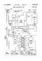
- FIG. 1is a block diagram of the overall switching module according to the invention.
- FIG. 2is a timing diagram for the control sequence of the switching module
- FIG. 3is a schematic diagram of the switch module input port
- FIG. 4is a schematic diagram of the switch module output port
- FIG. 5is a schematic diagram of a content addressable bit-map buffer memory allocation system according to one embodiment of the invention.
- FIG. 6illustrates a linked list buffer memory allocation system according to another embodiment of the invention.
- FIG. 7is a schematic diagram of a translator for interpreting data cells.
- FIG. 1The overall layout for the switch module according to the invention is illustrated in FIG. 1 including a shared buffer memory 100 which is used to store data cells while being transferred from an input port to selected output ports.
- datais transferred to and retrieved from memory 100 via a 32-bit data bus 102 and is addressed by means of a 13-bit address bus 104.
- a data cell according to ATM standardsincludes 53 octets (i.e. 53 8-bit bytes). One of these bytes is a header check sum which is removed at the input port after being used to check the header.
- the data cell with the check sum removedconsists of 52 8-bit bytes and can be stored in the buffer memory as 13 32-bit words. To simplify addressing, a 16-word space is allocated for each data cell even though only 13 words are required.
- a data cell addressis defined by the 9 most significant bits of the memory address, the remaining 4 bits being used to identify the location of the individual words making up the data cell.
- the first input port 110receives the incoming data cell in serial format via a cell receiver 112.
- One of the important functions of the cell receiveris to compare the header with the check sum contained in the fifth byte of data cell. If the header is valid, the check sum is removed and the remaining 52 bytes are passed on to a FIFO register 114.
- the FIFO registermust be capable of storing at least one complete data cell, and preferably as many as three data cells.
- the serial data cellis delineated and emerges as 52 8-bit bytes.
- the data cellpasses from FIFO 114 through a switch input port 116 where it is converted to a 32-bit word format.
- the data cellis then transferred into buffer memory 110 via a data bus 102 to a location determined by the address on address bus 104.
- the first output port 120(output port zero) is used to retrieve a data cell from a selected address via data bus 102.
- the data cellis received in a 32-bit word format by switch output port 126 and is passed on to a FIFO 124 in an 8-bit byte format.
- the data cellemerges from the FIFO and passes through a cell transmitter 122 which adds a header check sum as the fifth byte of the cell and transmits it in a serial format.
- the first input port 110 and the first output port 120are shown on the left and right, respectively, for ease of illustration. In an actual system the first port would normally include both input port 110 and output port 120 so that bidirectional communications can be established via a link connected to the port.
- the number of such ports in a switch moduleis a matter of engineering choice and depends largely on the desired operating speed for the module. For the illustrative embodiment a switch module with sixteen ports was selected.
- the input portseach similarly include a cell receiver 112, a FIFO 114 and a switch input port 116, whereas the output ports each include a switch output port 126, a FIFO 124 and a cell transmitter 122.
- the transceiver and cell delineation functionscan be achieved using commercially available chips.
- Transceivers operating at 155 Mb/sare available from TranSwitch as TXC-02301 and TXC-03003. Transceivers operating at 100 Mb/s are available from TranSwitch as AM7968 and AM7969. A suitable cell delineation block chip is available from TranSwitch as TXC 05150.
- the data transfer within the switch module and the buffer addressingis controlled by a cell manager 130 which includes a buffer memory allocation unit 132, a cell translator 134 and a sequencer 136.
- the cell managerhas access to data bus 102 and address bus 104.
- the cell manageris connected to activate a selected port via the port selection lines 138.
- the cell managersupplies addresses to the switch ports 116 and 126 as well as numerous control functions via connections not shown in FIG. 1.
- the header of the cellis transferred to translator 134 which determines the appropriate output port for the cell and the priority of the cell.
- the buffer memory allocation 132finds a vacant memory location and the incoming cell is transferred to that location on a word-by-word basis.
- the addressis also stored in a priority queue at the appropriate output port or ports. When the selected output port becomes available and the address is at the head of the queue, the corresponding data cell is retrieved from the buffer memory and transmitted from the selected port.
- Shared buffer memory 100can be of any size required by the switch. For the illustrative embodiment with sixteen input ports and sixteen output ports, a memory capable of storing 512 data cells was selected. These data cells are addressed by the nine most significant bits on the address bus. A data cell is stored in a sixteen 32-bit word space. A memory of 32K bytes is therefore selected for this illustrative embodiment.
- a control processor 150is coupled to cell manager 130.
- the principal task performed by the control processoris creating and deleting virtual paths (VP) and virtual circuits (VC) between the associated switch modules and other switches or interfaces in the network.
- the control processoris capable of receiving its own program and data in data cells from the network.
- the sequence for the various activities in the operation of the switch moduleis controlled by sequencer 136 shown in FIG. 1.
- the sequencerincludes a ROM (read only memory) addressed by a clock and counter combination operating in a closed repetitive sequence. In the chosen embodiment, which has 16 ports, a 24-bit word is stored in the ROM for each step in the sequence.
- the output bits from the ROMselectively control port selection, IN-translation read/write, OUT-translation read/write, buffer memory read/write, and cell release control.
- the repetitive sequenceis divided into 30 segments with each segment being further subdivided into 16 sectors, one sector for each of the ports in the switch module.
- the complete timing sequenceincludes 480 steps and therefore 480 words are stored in the ROM.
- the basic sequence of operations for an incoming data cellstarts with translation of the header to determine the appropriate output port and the cell priority.
- a vacant addressis allocated in the buffer memory and the incoming data cell is transferred to that address on a word-by-word basis.
- the storage of a word in memory using relatively inexpensive, commercially available componentsrequires about 18 nanoseconds.
- the translation and memory allocation operationsrequire on the order of 90 nanoseconds.
- the translation operationtherefore creates a bottleneck for the throughput of data through the switch.
- a similar bottleneckoccurs during the transmission of a data cell since, because of possible multicasting, a further translation operation is used to insure that the header is correct for each selected transmission link,
- the activity sequence according to the inventiontransfers data to and from the buffer memory on a word-by-word basis arranged so that the data transfers are not delayed by the slower translation and allocation functions.
- the activity sequenceis illustrated in FIG. 2 including a 30-sector primary sequence (to the left in the illustration) wherein each sector is subdivided into 16 segments with one segment for each port.
- the starting points for the word-by-word transfers of data cells from the different portsare distributed through the timing sequence so that the slower translation and allocation operations can be carried out while data is being transferred to and from the shared memory with respect to other ports.
- the first line of the sector portion of the timing sequence in FIG. 2is for sector "0" which is primarily for "write” operations where words of data can be transferred to the shared buffer memory from each of the input ports.
- the header translation operations for P0-IN (port zero--input translation), for P7-OUT (port seven--output translation), and P13-IN (port 13--input translation)are also initiated during sector zero.
- the sequence for sector "0"is set forth in greater detail in the segment/port activity portion of the illustration to the right in FIG. 2.
- segment "0"(of sector “0") the first word of the data cell, which includes the header, is transferred to translator 134 (FIG. 1) and the IN-TRAN translation commences to determine the cell priority and the appropriate output port. The results from the translation are stored in a FIFO register within translator 134 when the translation is completed.
- segment "1”the transfer of the data cell from port one is already underway and the 10th word of the data cell is transferred to the shared buffer memory.
- segments “2” to “6”the 6th, 2nd, 11th, 7th, and 3rd words from ports 2 to 6, respectively, are transferred to the shared memory.
- segment "7"the header from the data cell in output port 7 is transferred to translator 134 and the results of the OUT-TRAN translation are stored in a second FIFO register when completed.
- segments “8" to “12”the 8th, 4th, 12th, 9th, and 5th words from ports 8 to 12, respectively, are transferred to the shared memory.
- segment “13”the header from the data cell in input port thirteen is transferred to translator 134 and the results are stored in a third FIFO register within translator 134 when the IN-TRAN translation is completed.
- segments “14” and “15”the 10th and 6th words are transferred from ports fourteen and fifteen, respectively.
- Sector "1" of the timing sequenceis primarily for "read” operations, that is, retrieval of data cells from the shared memory by the output ports.
- the port 0 and port 13 data cell addressesare distributed (P0-Addr and P13-Addr) and the revised header for the outgoing link is received by port 7 (P7-Head). More specifically, during sector 1, segment 0, the results of the port zero translation for the incoming cell are in the first FIFO register of translator 134 and buffer memory allocation 132 indicates a vacant memory address.
- the vacant addressis sent to the first input port to control transfer of the data cell to the memory and is also sent to the appropriate output port together with the priority indication for the cell.
- the 12th, 8th and 4th words of the respective data cellsare delivered to output ports 1 to 3.
- the headeris transferred to output port 4.
- the 9th and 5th wordsare delivered to their respective output ports.
- the OUT-TRAN/Header operationtakes place where the modified header is transferred to output port 7.
- the 10th, 6th, 3rd, 11th and 7th wordsare transferred respectively to output ports 8 to 12.
- a vacant memory addressis transferred to input port 13 and to the selected outpost port.
- the 12th and 8th wordsare transferred to respective output ports 14 and 15.
- translator operations IN-TRAN and OUT-TRANare each separated by five or more segments. This separation permits the slow translator operations to be carried out while the faster word transfer operations go forward.
- the translator operationsare distributed more or less evenly throughout the activity sequence.
- the read and write operations for the words of the data cellcome in sequence after completion of the respective translation operations.
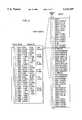
- the port activity sequenceas seen from port zero, is extracted from FIG. 2 and is set forth in the following table:
- the translationis performed during sector "0" and the vacant address for the incoming data cell is supplied to the ports in sector "1".
- the headeris written into the buffer memory in sector “2” and the following twelve words of the incoming data cell are written into memory in sectors "4", "6", "8", etc.
- Data word 4is transferred to output port zero in sector "3" and data words 5 to 12 are transferred in sectors "5", "7", “9", "11", "13", “15”, "17”, and "19".
- Switch module input port 116is shown schematically in FIG. 3.
- An incoming data cell including fifty-three octets (bytes)passes through the cell receiver 112 where the header is compared with the check sum in the cells. If the data cell is valid, the check sum is removed and the remaining fifty-two bytes are passed on to one or more FIFO's 114.
- the data cellis organized into 52 eight-bit bytes in FIFO 114.
- the data cellis transferred out of the FIFO in 9-bit words each including an 8-bit data byte and a 9th bit which is a "1" only if it accompanies the last byte of a data cell.
- the data cellis reorganized into 32-bit words in the switch module input port.
- a vacant buffer memory addressis assigned by buffer memory allocation unit 132.
- the data cellis then transferred to shared buffer memory 100 on a word-by-word basis under the control of sequencer 136.
- Shift register 302is a thirty-three-bit arrangement designed to receive 9-bit words from FIFO 114 via a 9-bit bus 340. Each 9-bit word includes an 8-bit byte of data plus a 9th bit which is "0" unless the word is the last word of a data cell.
- the transfer from FIFO 114 to register 302is controlled by a clock 332 which is part of cell receiver 112. When four data bytes have been transferred into register 302 and successively moved up in the register, register 302 is full including 32 data bits and a locator bit in the 33rd bit location 312.
- the 32-bit data word plus locator bitis transferred into a 12 ⁇ 33 FIFO register 303.
- the transfer into FIFO 303is achieved by dividing clock 232 by four in a divider 334.
- Divider 334provides a shift pulse for every 4 data bytes from FIFO 114.
- the 33rd bitis used for the locator bit which indicates the end of the data cell as it passes through FIFO 303.
- Registers 304 and 305are each 33-bit registers for transfer of the 32-bit words. These registers include bits 314 and 315 respectively, to provide cell location.
- Register 305is capable of receiving data from register 304 as well as from data bus 102.
- Register 305is also capable of transferring data to shared buffer memory 100 via data bus 102.
- An address unit 320is used to provide data addresses via bus 104 for locating transferred data in the shared buffer memory.
- the address unitincludes a 9-bit register 324 which receives data cell addresses from buffer memory allocation unit 132.
- the address unitalso includes a 4-bit counter 322 which provides the least significant bits of a memory address. To simplify addressing each data cell has a space allocation of sixteen 32-bit words, even though a 13-word space would be adequate for a data cell. This is done to simplify the addressing since, with the arrangement in the illustrative embodiment, each of the 9-bit words in register 324 is capable of defining a data cell space in memory.
- the 9-bit register 324can uniquely identify 512 data cell spaces in the shared memory, whereas counter 322 provides an additional 4 bits which define the individual word locations of the data cells.
- a 9-bit addressis transferred into register 324 and counter 322 is initially set to zero so that it points to the start of the space allocated for the data cell.
- Counter 322is advanced each time a data word is transferred to the memory so that address unit 320 always points to the address for the next word to be transferred from the input port to buffer memory 100.
- a read clock 336is controlled by sequencer 136 and a port input control unit 330 (through connections not shown).
- the read clockcontrols the transfer of data out of the FIFO register 303 and registers 304, and 305 into the buffer memory.
- the port input control 330receives signals from the locator bits 312-315 in the registers 302-305. Locator bits 312-315 indicate the location of the end of the data cell being passed through the registers.
- Control unit 330also receives an indication as to when FIFO 114 in the cell receiver is full and ready to transfer a data cell.
- the port input control 330further controls the in-clock for transfer of the data into the registers 302 and 303 as well as read clock 336 which controls the transfer of the data cell from registers 303-305 into shared memory 100.
- the operation of the switch module input port in FIG. 3starts with a data cell being received by the cell receiver which compares the check sum with the header to determine if a valid data cell has been received. If so, the check sum is removed and the remaining 52 bytes of the data cell are transferred into a FIFO 114.
- a data cellis transferred from FIFO 114 into registers 302 and 303. In the transfer through register 302 the 8-bit bytes are converted into 32-bit words.
- the transfer of the data cell into the shared memorycommences by stepping the data cell into registers 304 and 305 so that the cell header is located in register 305.
- the headeris transferred to translator 134 in the cell manager which examines the header and determines the appropriate output port and priority status of the data cell.
- the designated output port and priority statusare stored in one of the output FIFOs, such as 140.
- Buffer memory allocation unit 132provides a vacant memory address to address register 324.
- the transfer of the data cell to the vacant address in buffer memory 100 on a word-by-word basisis controlled by sequencer 136.
- the data cellis stepped to the right toward register 305 each time a word is transferred to the buffer memory via the data bus.
- Each transferalso advances the address counter 322 by one step so that the address unit 320 always points to the next word address.
- Each transfer of a data word to the shared memory via data bus 102is to the address to which the address unit 320 points via address bus 104.
- the switch module input portmust also include the capability of handling special meta signaling cells. Certain virtual paths and virtual circuits are set aside for signaling purposes. For example, a terminal station may request virtual path/virtual circuit information for reaching a certain destination. When such a meta cell is detected in the translator, the translation must provide a new header in addition to assigning a buffer space and selecting an outgoing port. The outgoing port will connect to the control processor 150, and the new header will distinguish which incoming port received the meta cell. Other traffic management cells may be received and detected by the translator. These cells require traffic information to be returned to the sender, so the requested information is inserted into the data section of the cell which is then returned to the originating terminal via the output port for the same link with an appropriately modified header.
- the switch module input portmust also be capable of receiving data cells which are addressed to control processor 150 associated with the switch module.
- the switch module output port 120retrieves data cells from shared memory 100 according to the addresses at the head of a priority queue.
- the number of priority classificationsis a matter of design, but a four-level priority appears to be adequate for most purposes and is used in the illustrative embodiment.
- the switch module output portincludes four separate priority queues, i.e. FIFOs 450-453.
- the FIFOsare each 10 bits wide in order to accept a 9-bit data cell address plus an additional bit for indicating congestion.
- the length of the FIFOis a matter of design depending on the anticipated needs.
- the capacity to store 16 addresses at each priority levelshould be adequate for most purposes and is used in the illustrative embodiment.
- the headeris transferred to cell translator 134 which determines the appropriate output port and the cell priority.
- Buffer memory allocation unit 132provides a vacant address for storing the incoming data cell. This address is sent to the selected output port via bus 455 and the priority information is provided to the priority assignment logic 460.
- the priority assignment logicdirects the incoming address to the priority FIFO 450-453 corresponding to the priority status.
- Each of the priority FIFOsare arranged to detect congested conditions when more than 12 addresses are in the priority queue. Any such congestion is indicated in the 10th bit associated with a 9-bit address.
- the switch module output portincludes an address unit 440 similar to the address unit in the switch module input port.
- the address unitincludes a 9-bit register 444 for the data cell address and a 4-bit counter 442 which points to the word address within the data cell.
- a next address select unit 462selects the address at the head of the highest priority queue and transfers that address to register 444 when a data cell is to be transmitted.
- Registers 410-413are used to receive the data cells from memory 100 via data bus 102 in a 32-bit word format.
- Register 410can receive a data word from the data bus or can supply a data word to the data bus.
- the first wordwhich is the header, is first transferred to register 410 from memory 100.
- the headeris then transferred from register 410 to translator 134 via the data bus and subsequently modified and returned to register 410.
- the data cellis then stepped into registers 410-412 word at a time under control of a write clock 436 through interconnections not shown in FIG. 4.
- the transfer of a data cell to cell transmitter 122 via register 413is controlled by an out clock 432 in the cell transmitter.
- the out clockcontrols the transfer of the data cell in 8-bit bytes from register 413 into 52 ⁇ 8 FIFO register 124.
- Out clock 432 divided by four in divider 433also controls the transfer of the data cell in 32-bit words from FIFO register 412.
- a 32-bit wordis transferred into register 413 and shifted downward and transferred into FIFO 124 as 8-bit bytes.
- the 33rd bit 420-423 of registers 410-413, respectively,is used for a locator bit which is a "1" for the last word of the data cell.
- the locator bitis inserted into the 33rd bit of register 410 by a port output port control 438.
- the port output controlis connected to monitor the locator bit as the data cell is stepped through registers 410-413.
- the locator bit 423is also connected to FIFO 124 in the cell transmitter to signal the end of a cell being transferred to the FIFO register.
- the switch module output portretrieves data cells from the shared memory according to the address at the head of the priority queue for the port.
- a data cellis received via an input port (FIG. 3)
- the header of the data cellis sent to cell translator 134 in the cell manager.
- the translatordetermines the appropriate output port for the cell and the priority of the cell.
- the buffer memory allocation unit 132determines a vacant address for storing the data cell in shared memory 100.
- the addressis sent to the output port via bus 455 (FIG. 4) and the priority indication is sent to priority assignment logic 460.
- the priority assignment logicdecodes the priority indication and gates the address into the appropriate one of the priority queue registers 450-453. If the priority register has more than a predetermined number of addresses already in the queue, priority assignment logic 460 adds a congestion indication to the 10th bit associated with the address.
- the output portretrieves data cells according to the addresses at the head of the highest order priority queue. More specifically, next address select unit 462 first retrieves data cells according to the addresses in the highest order priority queue 450, then retrieves data cells according to the addresses in the next highest priority queue 451 followed by retrieval according to addresses in the third priority queue 452 and, finally, retrieves data cells according to the addresses in the remaining priority queue, 453.
- the addresses from the priority queuesare transferred to the 9-bit address register 444 via bus 456.
- the 9-bit addresspoints to the starting point in the shared memory for the data cell.
- Counter 452which provides the four least significant bits of the memory address, is set to zero. Accordingly, the 13-bit address supplied to the memory via address bus 104 points to the word at the beginning of the data cell in the memory.
- the data cell at the designated addressis transferred from memory 100 to cell transmitter 122.
- the data cell as retrieved from memoryis in a 32-bit format.
- the data wordsare transferred a word at a time to register 410 via bus 102 and stepped into registers 411 and 412 as additional words arrive.
- the complete data celloccupies registers 410, 411 and 412.
- the first wordwhich is the 4-byte header for the cell, is transferred to the cell translator 134 for an update of the virtual path and virtual circuit in the header according to the link through which the data cell is to be transmitted. Such updating of the header is required in a multicasting situation where the same cell is being transmitted to several different destinations.
- the updated headeris transferred from the translator into register 410 via data bus 102.
- the subsequent words of the data cellare then shifted into registers 410-412.
- a locator bitis inserted in the 33rd-bit location of register 410 to indicate the end of the data cell.
- the location of the data cell, as it is stepped through the register,is determined by monitoring the 33rd-bits in segments 421-423.
- Register 413under the control of out clock 432 and divide-by-four divider unit 433 converts the 32-bit words of the data cell into 8-bit bytes for transfer into FIFO 124. After the data cell has been transferred to FIFO 124 in the cell transmitter, a check sum for the header is added as the fifth byte and the data cell is then transferred to the output link in a serial form.
- Buffer memory allocationcould theoretically be achieved by maintaining a bit map of all the assigned addresses and port assignments. Because of the multicasting possibility, the bit map must keep track of assigned addresses and each port from which the data cell at the address is to be transmitted. The bit map must be updated each time a data cell is transmitted and the buffer memory address must be indicated as free when all the intended data cell transmissions from a particular address have been completed. Such a memory allocation unit could be constructed using a 512 ⁇ 16 memory array and a search routine which would continue until a vacant address is found. Such a straight forward approach, however, would be unsatisfactory for many applications because of the large variation in the number of searches that may be required to find a free address and because of the time which may be required for the worst case search.
- FIG. 5One of the preferred buffer memory allocation unit embodiments according to the invention is illustrated in FIG. 5 using a 512 ⁇ 16 bit RAM buffer usage memory 520 in combination 512-bit array content addressable memory (CAM) 510.
- the buffer usage memoryis organized so that the port assignments for a data cell are reflected in the 16-bit word associated with the address assignment for the data cell.
- CAMarray content addressable memory
- Each time a data cell is transmittedthe address and port information for the transmitted data cell is sent to logic block 522 to erase the corresponding memory bit in usage memory 520.
- Content addressable memory 510includes a 512-bit memory array, i.e. one bit for each of the 512 assignable addresses in shared buffer memory 100.
- the bits in the CAMare automatically updated from buffer usage memory 520 via logic block 522 so that an address bit in the CAM becomes "0" when a data cell has been transmitted from all the assigned ports.
- Content addressable memory 510can be organized into any convenient bit array such as one including 512 bits arranged into 16 rows and 32 columns.
- the memory bits in the CAMare interconnected so that the memory can be searched row at a time or column at a time through the associated CAM control and address unit 516.
- the Cam control and address unitsearches all the rows in parallel at one time to locate the rows including one or more "0"s indicating free addresses using flow-through logic. The search then continues by examining the bits in a selected row to locate a free address.
- the search resultis a 9-bit address which is free in shared buffer memory 100.
- This addressis transferred from the CAM to a FIFO register 530.
- FIFO 530is capable of storing two addresses since the request for a second free address can be received before the first address is utilized.
- the end address unit 532functions as a latch for releasing the buffer usage bits.
- a content addressable memorywith characteristics similar to those described in the above-identified patent application Ser. No. 07/766,062 can be used.
- An alternative technique for assigning buffer memory addresses to incoming cellsis through a linked list as illustrated in FIG. 6.
- the linked listis set up in a memory associated with a microprocessor.
- the microprocessoris dedicated to the task of achieving a rapid address assignments as new cells arrive.
- the techniqueinvolves maintaining a linked list of the currently unassigned buffer memory addresses. When a buffer memory address is assigned to an incoming cell, the address is removed from the linked list. When a buffer memory address is released meaning that the data cell has been transmitted from all the assigned ports, the address is added to the end of the linked list. In this fashion, the system always maintains a current list of the unassigned buffer addresses available for assignment to incoming cells.
- the memory for the linked listis set up as illustrated in FIG. 6. All of the potentially available 512 memory addresses (in 9-bit form) are maintained on a permanent list, 610-615. Each buffer address has an assigned pointer 620-625 and a 16-bit space for port assignments 630-635. A head pointer 640 points to the head of the linked list, and a tail pointer 642 points to the end of the linked list. Initially, before any buffer addresses are assigned, the head pointer points to the first buffer address 610. The pointers associated with the buffer addresses each point to the next buffer address, e.g. pointer 620 points to buffer address 611, pointer 621 points to buffer address 612, etc. The tail pointer 642 points to the last buffer address 615.
- the buffer address pointed to by head pointer 640is assigned to the incoming cell.
- the pointer 620 associated with the assigned buffer memory addressis transferred to the head pointer, thereby removing the first buffer memory address from the linked list.
- the head pointeris pointing to the next buffer address 611, which is assigned, and the associated pointer, 621, is transferred to the head pointer.
- a buffer addressWhen a buffer address is released and available for reassignment, it is added to the end of the linked list. Each time a data cell is transmitted from an output port, the port assignment bit is changed to "0" and the 16-bit port assignment is checked to determine if any "1"s remain. If not, the address is released. The pointer to the newly released address is inserted as the pointer associated with the last buffer memory address then on the list as pointed to by tail pointer 642. The tail pointer is then reset so that it points to the newly added buffer address at the end of the list. In this manner the newly released buffer memory address is added to the end of the linked list.
- the initial linked listshows an orderly list progressing from top to bottom. In time the list will be modified so that the order appears to jump around in random fashion. The lack of order in the list, however, has no significant adverse effect on the operation of the linked list buffer addressing scheme.
- the function of translator 134is to receive the 32-bit header of a data cell to perform an IN-TRAN translation to determine the appropriate exit port and the cell priority or an OUT-TRAN translation to determine the virtual path and virtual circuit for the outgoing data cell which is to be transmitted.
- the OUT-TRAN translationbecomes necessary for multicasting where the same cell is sent to several destinations each having a different virtual path/virtual circuit.
- the ATM standardsprovide bits in the header for a range of 4k virtual path (“VP") addresses, and 64k virtual circuit (“VC”) addresses for each virtual path.
- VPvirtual path
- VCvirtual circuit
- the design of the data compressordepends on the number of VP/VC combinations the system is intended to service.
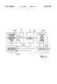
- An example of data compression for the translator in accordance with the inventionis achieved as illustrated in FIG. 7.
- Translator 134is located within the cell manager and responds to 12 bits for the virtual path designation, 16 bits for the virtual circuit designation, and 4 bits for the port designation.
- the cell managerextracts the 28-bit VP/VC designation from the data on the data bus and adds the 4-bit port designation according to the active port.
- the incoming 32 bitsare divided into two 16 bit groups 603 and 605 which are supplied respectively to 64k ⁇ 8 RAMs 602 and 604.
- the 8 bits 606 from memory 602 and the 8 bits 607 from memory 604are supplied as a 16-bit address to a 64k ⁇ 64 memory translation table 608.
- the translationemerges from memory 608 as a 64-bit word which includes 32 bits for the incoming IN-TRAN cell translation 620 and 32 bits for the outgoing OUT-TRAN translation 622.
- the IN-TRAN translation for an incoming data cellsupplies the outgoing port and priority for the cell.
- the OUT-TRAN translation for an outgoing data cellsupplies the virtual path and virtual circuit appropriate for the outgoing link.
- the 64-bit word emerging from memory 608is more than adequate for the translations and, hence, some spare bits are available for other purposes.
- the translation resultis placed in a selected one of three 64-bit FIFO registers 610.
- the allocation of the VP/VC and port bits to address RAMs 602 and 604is a matter of design choice depending largely upon the expected distribution of the virtual paths and virtual circuits.
- the contents of the 64k locations of the translation tableare set by control processor 150 shown in FIGS. 1 and 3.
- the control processorcreates and deletes the VP/VC addresses used in the translation table. Usually the VP/VC address information is maintained in the translation table only for the duration of a call.
Landscapes
- Engineering & Computer Science (AREA)
- Computer Networks & Wireless Communication (AREA)
- Signal Processing (AREA)
- Data Exchanges In Wide-Area Networks (AREA)
Abstract
Description
______________________________________ PORT ZERO ACTIVITY SEQUENCE Sector Action Data Port Cell ______________________________________ 0 Write Incoming Header (IN-TRAN) IN N 1 Read Buffer Address (result of IN- IN N TRAN/Addr) 2 Write Incoming header to buffer IN N 3 Read Data word 4 from buffer OUT M-1 4 Write Data word 1 to buffer IN N 5 Read Data word 5 from buffer OUT M-1 6 Write Data word 2 to buffer IN N 7 Read Data word 6 from buffer OUT M-1 8 Write Data word 3 to buffer IN N 9 Read Data word 7 from buffer OUT M-1 10 Write Data word 4 to buffer IN N 11 Read Data word 8 from buffer OUT M-1 12 Write Data word 5 to buffer IN N 13 Read Data word 9 from buffer OUT M-1 14 Write Data word 6 to buffer IN N 15 Read Data word 10 from buffer OUT M-1 16 Write Data word 7 to buffer IN N 17 Read Data word 11 from buffer OUT M-1 18 Write Data word 8 to buffer IN N 19 Read Data word 12 from buffer OUT M-1 20 Write Data word 9 to buffer IN N 21 Read Old outgoing header from buffer OUT M 22 Write Old outgoing header for OUT M OUT-TRAN 23 Read New outgoing header for OUT M OUT-TRAN 24 Write Data word 10 to buffer IN N 25 Read Data word 1 from buffer OUT M 26 Write Data word 11 to buffer IN N 27 Read Data word 2 to buffer OUT M 28 Write Data word 12 to buffer IN N 29 Read Data word 3 to buffer OUT M ______________________________________
Claims (55)
Priority Applications (1)
| Application Number | Priority Date | Filing Date | Title |
|---|---|---|---|
| US08/249,792US5535197A (en) | 1991-09-26 | 1994-05-25 | Shared buffer switching module |
Applications Claiming Priority (2)
| Application Number | Priority Date | Filing Date | Title |
|---|---|---|---|
| US76606291A | 1991-09-26 | 1991-09-26 | |
| US08/249,792US5535197A (en) | 1991-09-26 | 1994-05-25 | Shared buffer switching module |
Related Parent Applications (1)
| Application Number | Title | Priority Date | Filing Date |
|---|---|---|---|
| US76606291AContinuation-In-Part | 1991-09-26 | 1991-09-26 |
Publications (1)
| Publication Number | Publication Date |
|---|---|
| US5535197Atrue US5535197A (en) | 1996-07-09 |
Family
ID=46249079
Family Applications (1)
| Application Number | Title | Priority Date | Filing Date |
|---|---|---|---|
| US08/249,792Expired - LifetimeUS5535197A (en) | 1991-09-26 | 1994-05-25 | Shared buffer switching module |
Country Status (1)
| Country | Link |
|---|---|
| US (1) | US5535197A (en) |
Cited By (81)
| Publication number | Priority date | Publication date | Assignee | Title |
|---|---|---|---|---|
| WO1997004544A1 (en)* | 1995-07-19 | 1997-02-06 | Fujitsu Network Communications, Inc | Network switch utilizing centralized and partitioned memory for connection topology information storage |
| WO1997004561A1 (en)* | 1995-07-19 | 1997-02-06 | Fujitsu Network Communications, Inc. | Link scheduling |
| WO1997004562A1 (en)* | 1995-07-19 | 1997-02-06 | Fujitsu Network Communications, Inc. | Point-to-multipoint arbitration |
| WO1997004542A3 (en)* | 1995-07-19 | 1997-04-24 | Thomas A Manning | Multipoint-to-point arbitration in a network switch |
| US5684797A (en)* | 1995-04-05 | 1997-11-04 | International Business Machines Corporation | ATM cell multicasting method and apparatus |
| US5689505A (en)* | 1996-01-16 | 1997-11-18 | Lucent Technologies Inc. | Buffering of multicast cells in switching networks |
| US5724358A (en)* | 1996-02-23 | 1998-03-03 | Zeitnet, Inc. | High speed packet-switched digital switch and method |
| US5732079A (en)* | 1995-12-22 | 1998-03-24 | Cisco Technology, Inc. | Method and apparatus for skewing the start of transmission on multiple data highways |
| US5748905A (en) | 1996-08-30 | 1998-05-05 | Fujitsu Network Communications, Inc. | Frame classification using classification keys |
| US5761427A (en)* | 1994-12-28 | 1998-06-02 | Digital Equipment Corporation | Method and apparatus for updating host memory in an adapter to minimize host CPU overhead in servicing an interrupt |
| US5774453A (en)* | 1995-04-18 | 1998-06-30 | Nec Corporation | Input/output buffer type ATM switch |
| US5781533A (en) | 1995-07-19 | 1998-07-14 | Fujitsu Network Communications, Inc. | Link buffer sharing method and apparatus |
| US5787084A (en)* | 1996-06-05 | 1998-07-28 | Compaq Computer Corporation | Multicast data communications switching system and associated method |
| US5838677A (en)* | 1995-04-18 | 1998-11-17 | Hitachi, Ltd. | Switching system having means for congestion control by monitoring packets in a shared buffer and by suppressing the reading of packets from input buffers |
| WO1998038771A3 (en)* | 1997-02-27 | 1998-12-03 | Ericsson Telefon Ab L M | Flow control in switches |
| WO1998038760A3 (en)* | 1997-02-13 | 1998-12-17 | Mcdata Corp | Data communication system utilizing a scalable, non-blocking, high bandwidth central memory controller and method |
| WO1999008196A1 (en)* | 1997-08-12 | 1999-02-18 | Atmel Corporation | A universal serial bus device controller |
| US5898671A (en) | 1995-09-14 | 1999-04-27 | Fujitsu Network Communications, Inc. | Transmitter controlled flow control for buffer allocation in wide area ATM networks |
| US5898687A (en)* | 1996-07-24 | 1999-04-27 | Cisco Systems, Inc. | Arbitration mechanism for a multicast logic engine of a switching fabric circuit |
| US5914956A (en)* | 1997-02-03 | 1999-06-22 | Williams; Joel R. | Cache for improving the connection capacity of a communications switch |
| US5953315A (en)* | 1995-11-15 | 1999-09-14 | Nec Corporation | ATM cell sending system |
| US5991867A (en)* | 1996-09-12 | 1999-11-23 | Efficient Networks, Inc. | Transmit scheduler for an asynchronous transfer mode network and method of operation |
| US5991298A (en) | 1996-01-16 | 1999-11-23 | Fujitsu Network Communications, Inc. | Reliable and flexible multicast mechanism for ATM networks |
| US6011793A (en)* | 1995-07-11 | 2000-01-04 | Fujitsu Limited | Switching apparatus for simultaneously switching a plurality of switch units, with each switch unit including storage regions corresponding to other switch units |
| GB2341058A (en)* | 1998-08-28 | 2000-03-01 | Mitel Corp | Method for avoiding data loss in a packet switch |
| US6034954A (en)* | 1996-08-19 | 2000-03-07 | Hitachi, Ltd. | Multiplexing apparatus for transit of signals between service provided by low-speed transmission path and ATM service provided by high-speed transmission path |
| US6049891A (en)* | 1997-10-20 | 2000-04-11 | Fujitsu Limited | Data access control system and computer-readable medium storing data access control program |
| US6061348A (en)* | 1995-12-22 | 2000-05-09 | Cisco Technology, Inc. | Method and apparatus for dynamically allocating bandwidth for a time division multiplexed data bus |
| US6084880A (en)* | 1994-09-12 | 2000-07-04 | Efficient Networks, Inc. | Asynchronous transfer mode adapter for desktop applications |
| US6084881A (en)* | 1997-05-22 | 2000-07-04 | Efficient Networks, Inc. | Multiple mode xDSL interface |
| US6085250A (en)* | 1997-03-20 | 2000-07-04 | Efficient Networks, Inc. | Method and system for using layered networking application program interfaces (APIs) using a native asynchronous transfer mode (ATM) API |
| US6115771A (en)* | 1998-03-31 | 2000-09-05 | Lsi Logic Corporation | Method and system for converting computer peripheral equipment to SCSI-compliant devices |
| US6115374A (en)* | 1995-12-22 | 2000-09-05 | Cisco Technology, Inc. | Method and apparatus for dynamically assigning bandwidth for a time division multiplexing data bus |
| WO2000052858A1 (en)* | 1999-03-05 | 2000-09-08 | Transwitch Corporation | Method and apparatus for managing multiple atm cell queues |
| US6137807A (en)* | 1997-12-05 | 2000-10-24 | Whittaker Corporation | Dual bank queue memory and queue control system |
| US6233236B1 (en)* | 1999-01-12 | 2001-05-15 | Mcdata Corporation | Method and apparatus for measuring traffic within a switch |
| US6279050B1 (en)* | 1998-12-18 | 2001-08-21 | Emc Corporation | Data transfer apparatus having upper, lower, middle state machines, with middle state machine arbitrating among lower state machine side requesters including selective assembly/disassembly requests |
| US6289011B1 (en) | 1997-05-21 | 2001-09-11 | Samsung Electronics Co., Ltd. | 2n×n multiplexing switch |
| US6363075B1 (en)* | 1998-01-23 | 2002-03-26 | Industrial Technology Research Institute | Shared buffer management mechanism and method using multiple linked lists in a high speed packet switching system |
| WO2002034004A2 (en) | 2000-10-19 | 2002-04-25 | Interactic Holdings, Llc | Scaleable wormhole-routing concentrator |
| US6466580B1 (en)* | 1999-02-23 | 2002-10-15 | Advanced Micro Devices, Inc. | Method and apparatus for processing high and low priority frame data transmitted in a data communication system |
| WO2002093833A1 (en) | 2001-05-17 | 2002-11-21 | Alcatel Internetworking, Inc. | Distributed shared memory packet switch |
| US20020181456A1 (en)* | 2001-05-31 | 2002-12-05 | Fujitsu Limited | Switch device and data transfer system |
| US20030016688A1 (en)* | 2001-07-17 | 2003-01-23 | Hoof Werner Van | In-band message synchronization for distributed shared memory packet switch |
| US20030016689A1 (en)* | 2001-07-17 | 2003-01-23 | Hoof Werner Van | Switch fabric with dual port memory emulation scheme |
| US20030035372A1 (en)* | 2001-08-15 | 2003-02-20 | Marc Schaub | Method and system for managing packets in a shared memory buffer that serves multiple output links |
| US20030046496A1 (en)* | 2001-08-17 | 2003-03-06 | Mitchem William J. | Multi-rate shared memory architecture for frame storage and switching |
| US6567407B1 (en) | 1998-02-20 | 2003-05-20 | Nec Electronics Corporation | ATM switch circuit capable of increasing use efficiency of address memory, and ATM switch circuit controlling method |
| US6587898B1 (en)* | 2000-08-10 | 2003-07-01 | Dell Products, L.P. | Universal serial bus PC synchronization algorithm for peripheral devices |
| US6590897B1 (en) | 1999-03-08 | 2003-07-08 | Efficient Networks, Inc. | System and method for bridging universal serial bus and asynchronous transfer mode communication links |
| US6631484B1 (en) | 1998-03-31 | 2003-10-07 | Lsi Logic Corporation | System for packet communication where received packet is stored either in a FIFO or in buffer storage based on size of received packet |
| US20030191895A1 (en)* | 2002-04-03 | 2003-10-09 | Via Technologies, Inc | Buffer controller and management method thereof |
| US6636510B1 (en)* | 1998-05-28 | 2003-10-21 | Alcatel Canada Inc. | Multicast methodology and apparatus for backpressure-based switching fabric |
| US20030220959A1 (en)* | 2002-05-23 | 2003-11-27 | International Business Machines Corporation | Network processor which defines virtual paths without using logical path descriptors |
| US6657961B1 (en) | 1998-08-18 | 2003-12-02 | Efficient Networks, Inc. | System and method for enhanced end station to end station data flow control |
| US6661774B1 (en) | 1999-02-16 | 2003-12-09 | Efficient Networks, Inc. | System and method for traffic shaping packet-based signals |
| US6678279B1 (en) | 1999-12-13 | 2004-01-13 | Nortel Networks Limited | System and method to implement a packet switch buffer for unicast and multicast data |
| EP1195956A3 (en)* | 2000-10-03 | 2004-01-14 | Altima Communications, Inc. | Switch having flow control management |
| US20040028056A1 (en)* | 1999-01-12 | 2004-02-12 | Mitchem W. Jeffrey | Method for scoring queued frames for selective transmission through a switch |
| US6728857B1 (en)* | 2001-06-20 | 2004-04-27 | Cisco Technology, Inc. | Method and system for storing and retrieving data using linked lists |
| EP1120938A3 (en)* | 2000-01-28 | 2004-07-14 | VegaStream Ltd. | System using indirect memory addressing to perform cross-connecting of data transfers |
| US6804198B1 (en)* | 1999-05-24 | 2004-10-12 | Nec Corporation | ATM cell buffer system and its congestion control method |
| US6947415B1 (en)* | 1999-04-15 | 2005-09-20 | Nortel Networks Limited | Method and apparatus for processing packets in a routing switch |
| US20050254330A1 (en)* | 2002-01-03 | 2005-11-17 | John Mick | Apparatus and method for matrix memory switching element |
| US7031330B1 (en)* | 1999-04-15 | 2006-04-18 | Marconi Intellectual Property (Ringfence), Inc. | Very wide memory TDM switching system |
| US7046687B1 (en)* | 2002-01-16 | 2006-05-16 | Tau Networks | Configurable virtual output queues in a scalable switching system |
| US20060126653A1 (en)* | 2004-12-10 | 2006-06-15 | Matthew Joseph Anglin | Transferring data between system and storage in a shared buffer |
| US7075938B1 (en)* | 1998-03-13 | 2006-07-11 | Fujitsu Limited | Common buffer memory control apparatus |
| US7224693B1 (en)* | 2000-08-11 | 2007-05-29 | Ericsson Ab | Long packet handling |
| US20070274303A1 (en)* | 2005-01-05 | 2007-11-29 | Huawei Technologies Co., Ltd. | Buffer management method based on a bitmap table |
| US20080247411A1 (en)* | 2007-03-31 | 2008-10-09 | International Business Machines Corporation | Method to operate a crossbar switch |
| US20090097494A1 (en)* | 2007-10-15 | 2009-04-16 | Kuo-Hua Yuan | Packet forwarding method and device |
| USRE42443E1 (en) | 1999-04-05 | 2011-06-07 | Sandisk Il Ltd. | Architecture for a universal serial bus-based PC flash disk |
| US20110225531A1 (en)* | 2010-03-12 | 2011-09-15 | George Luis Irizarry | System and method for coordinating control of an output device by multiple control consoles |
| US20110225338A1 (en)* | 2010-03-12 | 2011-09-15 | George Luis Irizarry | Interface device for coordinating control of an output device by multiple control consoles |
| US20120317399A1 (en)* | 2010-04-14 | 2012-12-13 | International Business Machines Corporation | Performing A Local Reduction Operation On A Parallel Computer |
| WO2013170892A1 (en) | 2012-05-16 | 2013-11-21 | Siemens Aktiengesellschaft | Method and buffer device for transmitting messages of different classifications via buffers |
| US9459934B2 (en) | 2011-08-10 | 2016-10-04 | International Business Machines Corporation | Improving efficiency of a global barrier operation in a parallel computer |
| US9495135B2 (en) | 2012-02-09 | 2016-11-15 | International Business Machines Corporation | Developing collective operations for a parallel computer |
| US20170201468A1 (en)* | 2013-08-22 | 2017-07-13 | Mellanox Technologies, Ltd. | Packet switch with reduced latency |
| US20180246820A1 (en)* | 2017-02-24 | 2018-08-30 | Ati Technologies Ulc | Multiple linked list data structure |
Citations (12)
| Publication number | Priority date | Publication date | Assignee | Title |
|---|---|---|---|---|
| US3796835A (en)* | 1970-09-30 | 1974-03-12 | Ibm | Switching system for tdm data which induces an asynchronous submultiplex channel |
| US4603416A (en)* | 1982-12-29 | 1986-07-29 | Michel Servel | (Time division multiplex) switching system for routing trains of constant length data packets |
| US4823340A (en)* | 1986-12-05 | 1989-04-18 | Ant Nachrichtentechnik Gmbh | Circuit arrangement for non-blocking switching of PCM channels in the space and time domain |
| US4884264A (en)* | 1987-07-24 | 1989-11-28 | Etat Francais Represente Par Le Ministre Des Ptt (Centre National D'etudes Des Telecommunications | Hybrid time multiplex switching system with optimized buffer memory |
| US4939719A (en)* | 1987-11-27 | 1990-07-03 | Societe Anonyme Dite : Alcatel Cit | Management unit for a unit for switching data transmitted by asynchronous time-division multiplexing |
| US4939720A (en)* | 1987-11-27 | 1990-07-03 | Alcatel Cit | Unit for switching data transmitted by asynchronous time-division multiplexing |
| EP0388648A2 (en)* | 1989-02-22 | 1990-09-26 | Hitachi, Ltd. | Cell switching system for the time division multiplex communication |
| US5062106A (en)* | 1989-03-14 | 1991-10-29 | Kokusai Denshin Denwa Co., Ltd. | ATM exchange system |
| US5130979A (en)* | 1988-07-08 | 1992-07-14 | Nec Corporation | Frame converter using a dual-port random access memory |
| US5280475A (en)* | 1990-08-17 | 1994-01-18 | Hitachi, Ltd. | Traffic shaping method and circuit |
| US5303233A (en)* | 1990-05-18 | 1994-04-12 | Nec Corporation | Arrangement favorably carrying out a connection by the use of an intermediate conversion parameter between input and output virtual channel identifiers (VCI's) |
| US5365519A (en)* | 1991-03-05 | 1994-11-15 | Hitachi, Ltd. | ATM switch1ng system connectable to I/O links having different transmission rates |
- 1994
- 1994-05-25USUS08/249,792patent/US5535197A/ennot_activeExpired - Lifetime
Patent Citations (12)
| Publication number | Priority date | Publication date | Assignee | Title |
|---|---|---|---|---|
| US3796835A (en)* | 1970-09-30 | 1974-03-12 | Ibm | Switching system for tdm data which induces an asynchronous submultiplex channel |
| US4603416A (en)* | 1982-12-29 | 1986-07-29 | Michel Servel | (Time division multiplex) switching system for routing trains of constant length data packets |
| US4823340A (en)* | 1986-12-05 | 1989-04-18 | Ant Nachrichtentechnik Gmbh | Circuit arrangement for non-blocking switching of PCM channels in the space and time domain |
| US4884264A (en)* | 1987-07-24 | 1989-11-28 | Etat Francais Represente Par Le Ministre Des Ptt (Centre National D'etudes Des Telecommunications | Hybrid time multiplex switching system with optimized buffer memory |
| US4939719A (en)* | 1987-11-27 | 1990-07-03 | Societe Anonyme Dite : Alcatel Cit | Management unit for a unit for switching data transmitted by asynchronous time-division multiplexing |
| US4939720A (en)* | 1987-11-27 | 1990-07-03 | Alcatel Cit | Unit for switching data transmitted by asynchronous time-division multiplexing |
| US5130979A (en)* | 1988-07-08 | 1992-07-14 | Nec Corporation | Frame converter using a dual-port random access memory |
| EP0388648A2 (en)* | 1989-02-22 | 1990-09-26 | Hitachi, Ltd. | Cell switching system for the time division multiplex communication |
| US5062106A (en)* | 1989-03-14 | 1991-10-29 | Kokusai Denshin Denwa Co., Ltd. | ATM exchange system |
| US5303233A (en)* | 1990-05-18 | 1994-04-12 | Nec Corporation | Arrangement favorably carrying out a connection by the use of an intermediate conversion parameter between input and output virtual channel identifiers (VCI's) |
| US5280475A (en)* | 1990-08-17 | 1994-01-18 | Hitachi, Ltd. | Traffic shaping method and circuit |
| US5365519A (en)* | 1991-03-05 | 1994-11-15 | Hitachi, Ltd. | ATM switch1ng system connectable to I/O links having different transmission rates |
Non-Patent Citations (25)
| Title |
|---|
| Alles, A., ATM in Private Network, a Tutorial (Interop 93 Version), Hughes LAN Systems.* |
| Barri, P. and Goubert, J. A. O., "Implementation of a 16 to 16 Switching Element for ATM Exchanges", IEEE Journal on Selected Areas in Communications, vol. 9, No. 5, Jun., 1991, pp. 751-757. |
| Barri, P. and Goubert, J. A. O., Implementation of a 16 to 16 Switching Element for ATM Exchanges , IEEE Journal on Selected Areas in Communications, vol. 9, No. 5, Jun., 1991, pp. 751 757.* |
| Boettle, D. Henrion, M. A., "Alcatel ATM Switch Fabric and Its Properties", 1225 Electrical Communication 64 (1990) No. 2/3, Ramford, Essex, GB, pp. 156-165. |
| Boettle, D. Henrion, M. A., Alcatel ATM Switch Fabric and Its Properties , 1225 Electrical Communication 64 (1990) No. 2/3, Ramford, Essex, GB, pp. 156 165.* |
| DePrycker, M. et al., "An ATM Switching Architecture with Intrinsic Multicast Capabilities for the Belgian Broadband Experiment", Proceedings of the Int'l Switching Symposium, Stockholm, SE, May 28-Jun. 1, 1990, vol. V, pp. 111-118. |
| DePrycker, M. et al., An ATM Switching Architecture with Intrinsic Multicast Capabilities for the Belgian Broadband Experiment , Proceedings of the Int l Switching Symposium, Stockholm, SE, May 28 Jun. 1, 1990, vol. V, pp. 111 118.* |
| Eckberg, A. E. and Hou, T. -C., "Effects of Output Buffer Sharing on Buffer Requirements in an ATDM Packet Switch", Proceedings of the Seventh Annual Joint Conference of the IEEE Computer and Communications Soc., New Orleans, LA, Mar. 29-31, 1988, pp. 51.4.1-5A-4.8. |
| Eckberg, A. E. and Hou, T. C., Effects of Output Buffer Sharing on Buffer Requirements in an ATDM Packet Switch , Proceedings of the Seventh Annual Joint Conference of the IEEE Computer and Communications Soc., New Orleans, LA, Mar. 29 31, 1988, pp. 51.4.1 5A 4.8.* |
| Henrion, M. A. et al., "Switching Network Architecture for ATM Based Broadband Communications", Proceedings of the Int'l Switching Symposium, Stockholm, SE, May 28-Jun. 1, 1990, vol. V, pp. 1-8. |
| Henrion, M. A. et al., Switching Network Architecture for ATM Based Broadband Communications , Proceedings of the Int l Switching Symposium, Stockholm, SE, May 28 Jun. 1, 1990, vol. V, pp. 1 8.* |
| Horstmann, J. U., et al., "Metastability Behavior of CMOS ASIC Flip-Flops in Theory and Test", IEEE Journal of Solid-State Circuits, vol. 24, No. 1, Feb., 1989, pp. 146-157. |
| Horstmann, J. U., et al., Metastability Behavior of CMOS ASIC Flip Flops in Theory and Test , IEEE Journal of Solid State Circuits, vol. 24, No. 1, Feb., 1989, pp. 146 157.* |
| Karol, M. J., et al., "Input v. Output Queueing on a Space-Division Packet Switch", Conference Record IEEE Global Telecommunications Conference, Houston, TX, Dec. 1-4, 1986, pp. 19.4.1-19.4.7. |
| Karol, M. J., et al., Input v. Output Queueing on a Space Division Packet Switch , Conference Record IEEE Global Telecommunications Conference, Houston, TX, Dec. 1 4, 1986, pp. 19.4.1 19.4.7.* |
| Kleeman, L. and Cantoni, A., "Metastable Behavior in Digital Systems", IEEE Design & Test of Computers, Dec., 1987, pp. 4-19. |
| Kleeman, L. and Cantoni, A., Metastable Behavior in Digital Systems , IEEE Design & Test of Computers, Dec., 1987, pp. 4 19.* |
| Kuwahara, Hiroshi et al., "A shared buffer memory switch for an ATM exchange", Conference Record of the IEEE International Conference on Communications, vol. 1, pp. 4.4.1-4.4.5, Boston, MA, Jun. 11-14, 1989. |
| Kuwahara, Hiroshi et al., A shared buffer memory switch for an ATM exchange , Conference Record of the IEEE International Conference on Communications, vol. 1, pp. 4.4.1 4.4.5, Boston, MA, Jun. 11 14, 1989.* |
| Sakurai, Y. et al., "Large-Scale ATM Multistage Switching Network with Shared Buffer Memory Switches", IEEE Communications Magazine, Jan., 1991, pp. 90-96. |
| Sakurai, Y. et al., Large Scale ATM Multistage Switching Network with Shared Buffer Memory Switches , IEEE Communications Magazine, Jan., 1991, pp. 90 96.* |
| Sansom, R. D., "High-Performance ATM LAN Switches: Requirements and Architecture", Engineer Conference Notes Networld+Interop 94, Las Vegas, Nevada, May 4-5, 1994, pp. E6.1. |
| Sansom, R. D., High Performance ATM LAN Switches: Requirements and Architecture , Engineer Conference Notes Networld Interop 94, Las Vegas, Nevada, May 4 5, 1994, pp. E6.1.* |
| Veendrick, H. J. M., "The Behavior of Flip-Flops Used as Synchronizers and Prediction of Their Failure Rate", IEEE Journal of Solid-State Circuits, vol. SC-15, No. 2, Apr., 1980, pp. 169-176. |
| Veendrick, H. J. M., The Behavior of Flip Flops Used as Synchronizers and Prediction of Their Failure Rate , IEEE Journal of Solid State Circuits, vol. SC 15, No. 2, Apr., 1980, pp. 169 176.* |
Cited By (148)
| Publication number | Priority date | Publication date | Assignee | Title |
|---|---|---|---|---|
| US6084880A (en)* | 1994-09-12 | 2000-07-04 | Efficient Networks, Inc. | Asynchronous transfer mode adapter for desktop applications |
| US5761427A (en)* | 1994-12-28 | 1998-06-02 | Digital Equipment Corporation | Method and apparatus for updating host memory in an adapter to minimize host CPU overhead in servicing an interrupt |
| US5684797A (en)* | 1995-04-05 | 1997-11-04 | International Business Machines Corporation | ATM cell multicasting method and apparatus |
| AU710694B2 (en)* | 1995-04-18 | 1999-09-30 | Nec Corporation | An ATM switch |
| US5838677A (en)* | 1995-04-18 | 1998-11-17 | Hitachi, Ltd. | Switching system having means for congestion control by monitoring packets in a shared buffer and by suppressing the reading of packets from input buffers |
| US5774453A (en)* | 1995-04-18 | 1998-06-30 | Nec Corporation | Input/output buffer type ATM switch |
| US6011793A (en)* | 1995-07-11 | 2000-01-04 | Fujitsu Limited | Switching apparatus for simultaneously switching a plurality of switch units, with each switch unit including storage regions corresponding to other switch units |
| US5983260A (en) | 1995-07-19 | 1999-11-09 | Fujitsu Network Communications, Inc. | Serial control and data interconnects for coupling an I/O module with a switch fabric in a switch |
| US5982771A (en) | 1995-07-19 | 1999-11-09 | Fujitsu Network Communications, Inc. | Controlling bandwidth allocation using a pace counter |
| US6115748A (en) | 1995-07-19 | 2000-09-05 | Fujitsu Network Communications, Inc. | Prioritized access to shared buffers |
| WO1997004561A1 (en)* | 1995-07-19 | 1997-02-06 | Fujitsu Network Communications, Inc. | Link scheduling |
| US5781533A (en) | 1995-07-19 | 1998-07-14 | Fujitsu Network Communications, Inc. | Link buffer sharing method and apparatus |
| US6076112A (en) | 1995-07-19 | 2000-06-13 | Fujitsu Network Communications, Inc. | Prioritized access to shared buffers |
| US5790770A (en) | 1995-07-19 | 1998-08-04 | Fujitsu Network Communications, Inc. | Method and apparatus for reducing information loss in a communications network |
| US5822540A (en) | 1995-07-19 | 1998-10-13 | Fujitsu Network Communications, Inc. | Method and apparatus for discarding frames in a communications device |
| US6141346A (en) | 1995-07-19 | 2000-10-31 | Fujitsu Network Communications, Inc. | Point-to-multipoint transmission using subqueues |
| WO1997004544A1 (en)* | 1995-07-19 | 1997-02-06 | Fujitsu Network Communications, Inc | Network switch utilizing centralized and partitioned memory for connection topology information storage |
| US5850395A (en) | 1995-07-19 | 1998-12-15 | Fujitsu Network Communications, Inc. | Asynchronous transfer mode based service consolidation switch |
| US6426957B1 (en) | 1995-07-19 | 2002-07-30 | Fujitsu Network Communications, Inc. | Asynchronous transfer mode based service consolidation switch |
| US5862137A (en) | 1995-07-19 | 1999-01-19 | Fujitsu Network Communications, Inc. | Point-to-multipoint arbitration |
| US5867663A (en) | 1995-07-19 | 1999-02-02 | Fujitsu Network Communications, Inc. | Method and system for controlling network service parameters in a cell based communications network |
| US5870538A (en) | 1995-07-19 | 1999-02-09 | Fujitsu Network Communications, Inc. | Switch fabric controller comparator system and method |
| US5872769A (en) | 1995-07-19 | 1999-02-16 | Fujitsu Network Communications, Inc. | Linked list structures for multiple levels of control in an ATM switch |
| US6256674B1 (en) | 1995-07-19 | 2001-07-03 | Fujitsu Network Communications, Inc. | Method and apparatus for providing buffer state flow control at the link level in addition to flow control on a per-connection basis |
| US5889956A (en) | 1995-07-19 | 1999-03-30 | Fujitsu Network Communications, Inc. | Hierarchical resource management with maximum allowable allocation boundaries |
| US5896511A (en) | 1995-07-19 | 1999-04-20 | Fujitsu Network Communications, Inc. | Method and apparatus for providing buffer state flow control at the link level in addition to flow control on a per-connection basis |
| US6167452A (en) | 1995-07-19 | 2000-12-26 | Fujitsu Network Communications, Inc. | Joint flow control mechanism in a telecommunications network |
| WO1997004562A1 (en)* | 1995-07-19 | 1997-02-06 | Fujitsu Network Communications, Inc. | Point-to-multipoint arbitration |
| US5905729A (en) | 1995-07-19 | 1999-05-18 | Fujitsu Network Communications, Inc. | Mapping a data cell in a communication switch |
| US5909427A (en) | 1995-07-19 | 1999-06-01 | Fujitsu Network Communications, Inc. | Redundant switch system and method of operation |
| US6002667A (en) | 1995-07-19 | 1999-12-14 | Fujitsu Network Communications, Inc. | Minimum guaranteed cell rate method and apparatus |
| US5917805A (en) | 1995-07-19 | 1999-06-29 | Fujitsu Network Communications, Inc. | Network switch utilizing centralized and partitioned memory for connection topology information storage |
| US5933429A (en) | 1995-07-19 | 1999-08-03 | Fujitsu Network Communications, Inc. | Multipoint-to-multipoint echo processing in a network switch |
| US5948067A (en) | 1995-07-19 | 1999-09-07 | Fujitsu Network Communications, Inc. | Converting between an internal cell and multiple standard asynchronous transfer mode cells |
| US5996019A (en) | 1995-07-19 | 1999-11-30 | Fujitsu Network Communications, Inc. | Network link access scheduling using a plurality of prioritized lists containing queue identifiers |
| US5956342A (en) | 1995-07-19 | 1999-09-21 | Fujitsu Network Communications, Inc. | Priority arbitration for point-to-point and multipoint transmission |
| WO1997004542A3 (en)* | 1995-07-19 | 1997-04-24 | Thomas A Manning | Multipoint-to-point arbitration in a network switch |
| US6236655B1 (en) | 1995-07-19 | 2001-05-22 | Fujitsu Network Communications, Inc. | Port and link identification |
| US5978359A (en) | 1995-07-19 | 1999-11-02 | Fujitsu Network Communications, Inc. | Allocated and dynamic switch flow control |
| US6088736A (en) | 1995-07-19 | 2000-07-11 | Fujitsu Network Communications, Inc. | Joint flow control mechanism in a telecommunications network |
| US5982776A (en) | 1995-07-19 | 1999-11-09 | Fujitsu Network Communications, Inc. | Multipoint-to-point arbitration in a network switch |
| US5898671A (en) | 1995-09-14 | 1999-04-27 | Fujitsu Network Communications, Inc. | Transmitter controlled flow control for buffer allocation in wide area ATM networks |
| US5953315A (en)* | 1995-11-15 | 1999-09-14 | Nec Corporation | ATM cell sending system |
| US6061348A (en)* | 1995-12-22 | 2000-05-09 | Cisco Technology, Inc. | Method and apparatus for dynamically allocating bandwidth for a time division multiplexed data bus |
| US6115374A (en)* | 1995-12-22 | 2000-09-05 | Cisco Technology, Inc. | Method and apparatus for dynamically assigning bandwidth for a time division multiplexing data bus |
| US5732079A (en)* | 1995-12-22 | 1998-03-24 | Cisco Technology, Inc. | Method and apparatus for skewing the start of transmission on multiple data highways |
| US5991298A (en) | 1996-01-16 | 1999-11-23 | Fujitsu Network Communications, Inc. | Reliable and flexible multicast mechanism for ATM networks |
| US5689505A (en)* | 1996-01-16 | 1997-11-18 | Lucent Technologies Inc. | Buffering of multicast cells in switching networks |
| US5724358A (en)* | 1996-02-23 | 1998-03-03 | Zeitnet, Inc. | High speed packet-switched digital switch and method |
| US5787084A (en)* | 1996-06-05 | 1998-07-28 | Compaq Computer Corporation | Multicast data communications switching system and associated method |
| US5898687A (en)* | 1996-07-24 | 1999-04-27 | Cisco Systems, Inc. | Arbitration mechanism for a multicast logic engine of a switching fabric circuit |
| US6034954A (en)* | 1996-08-19 | 2000-03-07 | Hitachi, Ltd. | Multiplexing apparatus for transit of signals between service provided by low-speed transmission path and ATM service provided by high-speed transmission path |
| US5748905A (en) | 1996-08-30 | 1998-05-05 | Fujitsu Network Communications, Inc. | Frame classification using classification keys |
| US5991867A (en)* | 1996-09-12 | 1999-11-23 | Efficient Networks, Inc. | Transmit scheduler for an asynchronous transfer mode network and method of operation |
| US5914956A (en)* | 1997-02-03 | 1999-06-22 | Williams; Joel R. | Cache for improving the connection capacity of a communications switch |
| US6061358A (en)* | 1997-02-13 | 2000-05-09 | Mcdata Corporation | Data communication system utilizing a scalable, non-blocking, high bandwidth central memory controller and method |
| WO1998038760A3 (en)* | 1997-02-13 | 1998-12-17 | Mcdata Corp | Data communication system utilizing a scalable, non-blocking, high bandwidth central memory controller and method |
| WO1998038771A3 (en)* | 1997-02-27 | 1998-12-03 | Ericsson Telefon Ab L M | Flow control in switches |
| US6085250A (en)* | 1997-03-20 | 2000-07-04 | Efficient Networks, Inc. | Method and system for using layered networking application program interfaces (APIs) using a native asynchronous transfer mode (ATM) API |
| US6289011B1 (en) | 1997-05-21 | 2001-09-11 | Samsung Electronics Co., Ltd. | 2n×n multiplexing switch |
| US6084881A (en)* | 1997-05-22 | 2000-07-04 | Efficient Networks, Inc. | Multiple mode xDSL interface |
| WO1999008196A1 (en)* | 1997-08-12 | 1999-02-18 | Atmel Corporation | A universal serial bus device controller |
| US5974486A (en)* | 1997-08-12 | 1999-10-26 | Atmel Corporation | Universal serial bus device controller comprising a FIFO associated with a plurality of endpoints and a memory for storing an identifier of a current endpoint |
| US6049891A (en)* | 1997-10-20 | 2000-04-11 | Fujitsu Limited | Data access control system and computer-readable medium storing data access control program |
| US6137807A (en)* | 1997-12-05 | 2000-10-24 | Whittaker Corporation | Dual bank queue memory and queue control system |
| US6363075B1 (en)* | 1998-01-23 | 2002-03-26 | Industrial Technology Research Institute | Shared buffer management mechanism and method using multiple linked lists in a high speed packet switching system |
| US6567407B1 (en) | 1998-02-20 | 2003-05-20 | Nec Electronics Corporation | ATM switch circuit capable of increasing use efficiency of address memory, and ATM switch circuit controlling method |
| US7075938B1 (en)* | 1998-03-13 | 2006-07-11 | Fujitsu Limited | Common buffer memory control apparatus |
| US6115771A (en)* | 1998-03-31 | 2000-09-05 | Lsi Logic Corporation | Method and system for converting computer peripheral equipment to SCSI-compliant devices |
| US6631484B1 (en) | 1998-03-31 | 2003-10-07 | Lsi Logic Corporation | System for packet communication where received packet is stored either in a FIFO or in buffer storage based on size of received packet |
| US6636510B1 (en)* | 1998-05-28 | 2003-10-21 | Alcatel Canada Inc. | Multicast methodology and apparatus for backpressure-based switching fabric |
| US6657961B1 (en) | 1998-08-18 | 2003-12-02 | Efficient Networks, Inc. | System and method for enhanced end station to end station data flow control |
| GB2341058A (en)* | 1998-08-28 | 2000-03-01 | Mitel Corp | Method for avoiding data loss in a packet switch |
| US6279050B1 (en)* | 1998-12-18 | 2001-08-21 | Emc Corporation | Data transfer apparatus having upper, lower, middle state machines, with middle state machine arbitrating among lower state machine side requesters including selective assembly/disassembly requests |
| US20040028056A1 (en)* | 1999-01-12 | 2004-02-12 | Mitchem W. Jeffrey | Method for scoring queued frames for selective transmission through a switch |
| US6233236B1 (en)* | 1999-01-12 | 2001-05-15 | Mcdata Corporation | Method and apparatus for measuring traffic within a switch |
| US7382736B2 (en) | 1999-01-12 | 2008-06-03 | Mcdata Corporation | Method for scoring queued frames for selective transmission through a switch |
| US7848253B2 (en) | 1999-01-12 | 2010-12-07 | Mcdata Corporation | Method for scoring queued frames for selective transmission through a switch |
| US6661774B1 (en) | 1999-02-16 | 2003-12-09 | Efficient Networks, Inc. | System and method for traffic shaping packet-based signals |
| US6466580B1 (en)* | 1999-02-23 | 2002-10-15 | Advanced Micro Devices, Inc. | Method and apparatus for processing high and low priority frame data transmitted in a data communication system |
| CN100512065C (en)* | 1999-03-05 | 2009-07-08 | Tr科技基金有限责任公司 | Method and apparatus for managing a plurality of ATM cell queues |
| WO2000052858A1 (en)* | 1999-03-05 | 2000-09-08 | Transwitch Corporation | Method and apparatus for managing multiple atm cell queues |
| US6246682B1 (en)* | 1999-03-05 | 2001-06-12 | Transwitch Corp. | Method and apparatus for managing multiple ATM cell queues |
| US6590897B1 (en) | 1999-03-08 | 2003-07-08 | Efficient Networks, Inc. | System and method for bridging universal serial bus and asynchronous transfer mode communication links |
| USRE42443E1 (en) | 1999-04-05 | 2011-06-07 | Sandisk Il Ltd. | Architecture for a universal serial bus-based PC flash disk |
| USRE44641E1 (en) | 1999-04-05 | 2013-12-10 | Sandisk Il, Ltd | USB flash memory device with integrated USB controller |
| USRE44653E1 (en) | 1999-04-05 | 2013-12-17 | Sandisk Il, Ltd | USB flash memory device with integral memory technology driver |
| US7031330B1 (en)* | 1999-04-15 | 2006-04-18 | Marconi Intellectual Property (Ringfence), Inc. | Very wide memory TDM switching system |
| US6947415B1 (en)* | 1999-04-15 | 2005-09-20 | Nortel Networks Limited | Method and apparatus for processing packets in a routing switch |
| US6804198B1 (en)* | 1999-05-24 | 2004-10-12 | Nec Corporation | ATM cell buffer system and its congestion control method |
| US6678279B1 (en) | 1999-12-13 | 2004-01-13 | Nortel Networks Limited | System and method to implement a packet switch buffer for unicast and multicast data |
| EP1120938A3 (en)* | 2000-01-28 | 2004-07-14 | VegaStream Ltd. | System using indirect memory addressing to perform cross-connecting of data transfers |
| US6587898B1 (en)* | 2000-08-10 | 2003-07-01 | Dell Products, L.P. | Universal serial bus PC synchronization algorithm for peripheral devices |
| US7224693B1 (en)* | 2000-08-11 | 2007-05-29 | Ericsson Ab | Long packet handling |
| EP1195956A3 (en)* | 2000-10-03 | 2004-01-14 | Altima Communications, Inc. | Switch having flow control management |
| US6851000B2 (en) | 2000-10-03 | 2005-02-01 | Broadcom Corporation | Switch having flow control management |
| US20050073957A1 (en)* | 2000-10-03 | 2005-04-07 | Broadcom Corporation | Switch having flow control management |
| US6687253B1 (en) | 2000-10-19 | 2004-02-03 | Interactic Holdings, Llc | Scaleable wormhole-routing concentrator |
| WO2002034004A3 (en)* | 2000-10-19 | 2003-03-13 | Interactic Holdings Llc | Scaleable wormhole-routing concentrator |
| CN100397373C (en)* | 2000-10-19 | 2008-06-25 | 英特拉克蒂克控股公司 | Scalable Wormhole Routing Concentrator |
| WO2002034004A2 (en) | 2000-10-19 | 2002-04-25 | Interactic Holdings, Llc | Scaleable wormhole-routing concentrator |
| WO2002093833A1 (en) | 2001-05-17 | 2002-11-21 | Alcatel Internetworking, Inc. | Distributed shared memory packet switch |
| US7339944B2 (en) | 2001-05-17 | 2008-03-04 | Alcatel Lucent | Distributed shared memory packet switch |
| US20030002509A1 (en)* | 2001-05-17 | 2003-01-02 | Jan Vandenhoudt | Distributed shared memory packet switch |
| US20020181456A1 (en)* | 2001-05-31 | 2002-12-05 | Fujitsu Limited | Switch device and data transfer system |
| US6728857B1 (en)* | 2001-06-20 | 2004-04-27 | Cisco Technology, Inc. | Method and system for storing and retrieving data using linked lists |
| US20030016689A1 (en)* | 2001-07-17 | 2003-01-23 | Hoof Werner Van | Switch fabric with dual port memory emulation scheme |
| WO2003009543A3 (en)* | 2001-07-17 | 2003-04-03 | Alcatel Internetworking Inc | In-band message synchronization for distributed shared memory packet switch |
| CN100370784C (en)* | 2001-07-17 | 2008-02-20 | 阿尔卡特互联网运行公司 | In-Band Message Synchronization for Distributed Shared Memory Packet Switches |
| US7203193B2 (en) | 2001-07-17 | 2007-04-10 | Alcatel Lucent | In-band message synchronization for distributed shared memory packet switch |
| US20030016688A1 (en)* | 2001-07-17 | 2003-01-23 | Hoof Werner Van | In-band message synchronization for distributed shared memory packet switch |
| US7031331B2 (en) | 2001-08-15 | 2006-04-18 | Riverstone Networks, Inc. | Method and system for managing packets in a shared memory buffer that serves multiple output links |
| US20030035372A1 (en)* | 2001-08-15 | 2003-02-20 | Marc Schaub | Method and system for managing packets in a shared memory buffer that serves multiple output links |
| US7054312B2 (en)* | 2001-08-17 | 2006-05-30 | Mcdata Corporation | Multi-rate shared memory architecture for frame storage and switching |
| US20030046496A1 (en)* | 2001-08-17 | 2003-03-06 | Mitchem William J. | Multi-rate shared memory architecture for frame storage and switching |
| US20050254330A1 (en)* | 2002-01-03 | 2005-11-17 | John Mick | Apparatus and method for matrix memory switching element |
| US7715377B2 (en)* | 2002-01-03 | 2010-05-11 | Integrated Device Technology, Inc. | Apparatus and method for matrix memory switching element |
| US7046687B1 (en)* | 2002-01-16 | 2006-05-16 | Tau Networks | Configurable virtual output queues in a scalable switching system |
| US20050289255A1 (en)* | 2002-04-02 | 2005-12-29 | Via Technologies, Inc. | Buffer controller and management method thereof |
| US20030191895A1 (en)* | 2002-04-03 | 2003-10-09 | Via Technologies, Inc | Buffer controller and management method thereof |
| US7536488B2 (en) | 2002-04-03 | 2009-05-19 | Via Technologies, Inc. | Buffer controller and management method thereof |
| US7930451B2 (en) | 2002-04-03 | 2011-04-19 | Via Technologies | Buffer controller and management method thereof |
| US7000073B2 (en)* | 2002-04-03 | 2006-02-14 | Via Technologies, Inc. | Buffer controller and management method thereof |
| US20030220959A1 (en)* | 2002-05-23 | 2003-11-27 | International Business Machines Corporation | Network processor which defines virtual paths without using logical path descriptors |
| US7069557B2 (en)* | 2002-05-23 | 2006-06-27 | International Business Machines Corporation | Network processor which defines virtual paths without using logical path descriptors |
| US20060126653A1 (en)* | 2004-12-10 | 2006-06-15 | Matthew Joseph Anglin | Transferring data between system and storage in a shared buffer |
| US7590777B2 (en)* | 2004-12-10 | 2009-09-15 | International Business Machines Corporation | Transferring data between system and storage in a shared buffer |
| US20070274303A1 (en)* | 2005-01-05 | 2007-11-29 | Huawei Technologies Co., Ltd. | Buffer management method based on a bitmap table |
| US7733892B2 (en)* | 2005-01-05 | 2010-06-08 | Huawei Technologies Co., Ltd. | Buffer management method based on a bitmap table |
| US20080247411A1 (en)* | 2007-03-31 | 2008-10-09 | International Business Machines Corporation | Method to operate a crossbar switch |
| US7978690B2 (en)* | 2007-03-31 | 2011-07-12 | International Business Machines Corporation | Method to operate a crossbar switch |
| TWI397285B (en)* | 2007-10-15 | 2013-05-21 | Realtek Semiconductor Corp | Packet transfer method |
| US8363653B2 (en)* | 2007-10-15 | 2013-01-29 | Realtek Semiconductor Corp. | Packet forwarding method and device |
| US20090097494A1 (en)* | 2007-10-15 | 2009-04-16 | Kuo-Hua Yuan | Packet forwarding method and device |
| US20110225338A1 (en)* | 2010-03-12 | 2011-09-15 | George Luis Irizarry | Interface device for coordinating control of an output device by multiple control consoles |
| US20110225531A1 (en)* | 2010-03-12 | 2011-09-15 | George Luis Irizarry | System and method for coordinating control of an output device by multiple control consoles |
| US8656081B2 (en)* | 2010-03-12 | 2014-02-18 | The United States Of America As Represented By The Secretary Of The Navy | System and method for coordinating control of an output device by multiple control consoles |
| US8667206B2 (en)* | 2010-03-12 | 2014-03-04 | The United States Of America As Represented By The Secretary Of The Navy | Interface device for coordinating control of an output device by multiple control consoles |
| US8458244B2 (en)* | 2010-04-14 | 2013-06-04 | International Business Machines Corporation | Performing a local reduction operation on a parallel computer |
| US20120317399A1 (en)* | 2010-04-14 | 2012-12-13 | International Business Machines Corporation | Performing A Local Reduction Operation On A Parallel Computer |
| US9459934B2 (en) | 2011-08-10 | 2016-10-04 | International Business Machines Corporation | Improving efficiency of a global barrier operation in a parallel computer |
| US9501265B2 (en) | 2012-02-09 | 2016-11-22 | International Business Machines Corporation | Developing collective operations for a parallel computer |
| US9495135B2 (en) | 2012-02-09 | 2016-11-15 | International Business Machines Corporation | Developing collective operations for a parallel computer |
| WO2013170892A1 (en) | 2012-05-16 | 2013-11-21 | Siemens Aktiengesellschaft | Method and buffer device for transmitting messages of different classifications via buffers |
| US20170201468A1 (en)* | 2013-08-22 | 2017-07-13 | Mellanox Technologies, Ltd. | Packet switch with reduced latency |
| US10462075B2 (en)* | 2013-08-22 | 2019-10-29 | Mellanox Technologies, Ltd. | Packet switch with reduced latency |
| US20180246820A1 (en)* | 2017-02-24 | 2018-08-30 | Ati Technologies Ulc | Multiple linked list data structure |
| US10545887B2 (en)* | 2017-02-24 | 2020-01-28 | Ati Technologies Ulc | Multiple linked list data structure |
Similar Documents
| Publication | Publication Date | Title |
|---|---|---|
| US5535197A (en) | Shared buffer switching module | |
| AU693084B2 (en) | Controlled access ATM switch | |
| AU637250B2 (en) | Traffic shaping method and circuit | |
| US5463621A (en) | Fast connection setup interfaces using pre-assigned virtual channel identifiers | |
| US5271004A (en) | Asynchronous transfer mode switching arrangement providing broadcast transmission | |
| EP0299473B1 (en) | Switching system and method of construction thereof | |
| JP3443264B2 (en) | Improved multicast routing in multistage networks | |
| EP0858718B1 (en) | Improvements in or relating to an atm switch | |
| CA2022798C (en) | Communication switching element and method for transmitting variable length cells | |
| US5202885A (en) | Atm exchange with copying capability | |
| EP0785698B1 (en) | Buffering of multicast cells in switching networks | |
| EP0195589B1 (en) | Switching system for transmission of data | |
| US6611527B1 (en) | Packet switching apparatus with a common buffer | |
| US5418781A (en) | Architecture for maintaining the sequence of packet cells transmitted over a multicast, cell-switched network | |
| EP0742677A2 (en) | Header converting method | |
| EP0828403B1 (en) | Improvements in or relating to an ATM switch | |
| JPH10215260A (en) | Routing switch for bidirectional transmission of digital signals | |
| US5434855A (en) | Method and apparatus for selective interleaving in a cell-switched network | |
| US6144640A (en) | ATM switch | |
| EP0612171B1 (en) | Data queueing apparatus and ATM cell switch based on shifting and searching | |
| US6493315B1 (en) | ATM switch for routing different cell types | |
| RU2134024C1 (en) | Device and method of processing of elements of data on mode of asynchronous transmission in system of commutation of mode of asynchronous transmission | |
| EP0870415A1 (en) | Switching apparatus | |
| KR960011972B1 (en) | Header converter and its method for virtual channel and virtual path simultaneously | |
| JPH0879261A (en) | ATM switching device and method |
Legal Events
| Date | Code | Title | Description |
|---|---|---|---|
| AS | Assignment | Owner name:IPC INFORMATION SYSTEMS, INC., CONNECTICUT Free format text:ASSIGNMENT OF ASSIGNORS INTEREST;ASSIGNOR:COTTON, JOHN M.;REEL/FRAME:007073/0135 Effective date:19940512 | |
| AS | Assignment | Owner name:IPC INFORMATION SYSTEMS, INC., NEW YORK Free format text:RELEASE OF SECURITY INTEREST;ASSIGNOR:CIT GROUP/CREDIT FINANCE, INC., THE;REEL/FRAME:007936/0246 Effective date:19950727 | |
| STCF | Information on status: patent grant | Free format text:PATENTED CASE | |
| AS | Assignment | Owner name:MORGAN STANLEY SENIOR FUNDING, INC., AS ADMINISTRA Free format text:COLLATERAL ASSIGNMENT;ASSIGNOR:IPC INFORMATION SYSTEMS, INC.;REEL/FRAME:009214/0619 Effective date:19980430 Owner name:MORGAN STANELY SENIOR FUNDING, INC., AS ADMINISTRA Free format text:COLLATERAL ASSIGNMENT;ASSIGNOR:IPC INFORMATION SYSTEMS, INC.;REEL/FRAME:009214/0626 Effective date:19980430 | |
| AS | Assignment | Owner name:GENERAL ELECTRIC CAPITAL CORPORATION, CONNECTICUT Free format text:AMENDMENT TO COLLATERAL ASSIGNMENT OF SECURITY INTEREST IN PATENTS;ASSIGNORS:MORGAN STANLEY SENIOR FUNDING, INC.;IPC INFORMATION SYSTEMS, INC.;REEL/FRAME:009693/0261 Effective date:19981201 | |
| FEPP | Fee payment procedure | Free format text:PAYOR NUMBER ASSIGNED (ORIGINAL EVENT CODE: ASPN); ENTITY STATUS OF PATENT OWNER: LARGE ENTITY | |
| REMI | Maintenance fee reminder mailed | ||
| FPAY | Fee payment | Year of fee payment:4 | |
| SULP | Surcharge for late payment | ||
| AS | Assignment | Owner name:IPC INFORMATION SYSTEMS, INC., NEW YORK Free format text:RELEASE OF SECURITY INTEREST;ASSIGNOR:GENERAL ELECTRIC CAPITAL CORPORATION, AS ADMINISTRATIVE AGENT (NY CORPORATION);REEL/FRAME:011667/0445 Effective date:20000613 | |
| AS | Assignment | Owner name:GENERAL ELECTRIC CAPITAL CORP., AS COLLATERAL AGEN Free format text:AMENDED AND RESTATED PLEDGE AND SECURITY AGREEMENT;ASSIGNORS:IPC ACQUISITION CORP.;IPC INFORMATION SYSTEMS, INC.;IPC FUNDING CORP.;AND OTHERS;REEL/FRAME:013943/0570 Effective date:20030829 | |
| FPAY | Fee payment | Year of fee payment:8 | |
| AS | Assignment | Owner name:IPC INFORMATION SYSTEMS, LLC, DELAWARE Free format text:CHANGE OF NAME;ASSIGNOR:IPC INFORMATION SYSTEMS, INC.;REEL/FRAME:014313/0655 Effective date:20031231 | |
| AS | Assignment | Owner name:IPC FUNDING CORP., NEW YORK Free format text:RELEASE OF SECURITY INTEREST AT REEL/FRAME NO. 13943/0570;ASSIGNOR:GENERAL ELECTRIC CAPITAL CORPORATION;REEL/FRAME:016377/0453 Effective date:20050805 Owner name:IPC ACQUISITION CORP., NEW YORK Free format text:RELEASE OF SECURITY INTEREST AT REEL/FRAME NO. 13943/0570;ASSIGNOR:GENERAL ELECTRIC CAPITAL CORPORATION;REEL/FRAME:016377/0453 Effective date:20050805 Owner name:IPC INFORMATION SYSTEMS FAR EAST INC., NEW YORK Free format text:RELEASE OF SECURITY INTEREST AT REEL/FRAME NO. 13943/0570;ASSIGNOR:GENERAL ELECTRIC CAPITAL CORPORATION;REEL/FRAME:016377/0453 Effective date:20050805 Owner name:V BAND CORPORATION, NEW YORK Free format text:RELEASE OF SECURITY INTEREST AT REEL/FRAME NO. 13943/0570;ASSIGNOR:GENERAL ELECTRIC CAPITAL CORPORATION;REEL/FRAME:016377/0453 Effective date:20050805 Owner name:IPC INFORMATION SYSTEMS HOLDINGS USA, L.L.C., NEW Free format text:RELEASE OF SECURITY INTEREST AT REEL/FRAME NO. 13943/0570;ASSIGNOR:GENERAL ELECTRIC CAPITAL CORPORATION;REEL/FRAME:016377/0453 Effective date:20050805 Owner name:IPC NETWORK SERVICES, INC. (F/K/A GAINS INTERNATIO Free format text:RELEASE OF SECURITY INTEREST AT REEL/FRAME NO. 13943/0570;ASSIGNOR:GENERAL ELECTRIC CAPITAL CORPORATION;REEL/FRAME:016377/0453 Effective date:20050805 Owner name:IPC INFORMATION SYSTEMS HOLDINGS USA, INC., NEW YO Free format text:RELEASE OF SECURITY INTEREST AT REEL/FRAME NO. 13943/0570;ASSIGNOR:GENERAL ELECTRIC CAPITAL CORPORATION;REEL/FRAME:016377/0453 Effective date:20050805 Owner name:IPC INFORMATION SYSTEMS HOLDINGS, INC., NEW YORK Free format text:RELEASE OF SECURITY INTEREST AT REEL/FRAME NO. 13943/0570;ASSIGNOR:GENERAL ELECTRIC CAPITAL CORPORATION;REEL/FRAME:016377/0453 Effective date:20050805 Owner name:IPC INFORMATION SYSTEMS SERVICES, L.L.C., NEW YORK Free format text:RELEASE OF SECURITY INTEREST AT REEL/FRAME NO. 13943/0570;ASSIGNOR:GENERAL ELECTRIC CAPITAL CORPORATION;REEL/FRAME:016377/0453 Effective date:20050805 Owner name:IPC INFORMATION SYSTEMS SERVICES, INC., NEW YORK Free format text:RELEASE OF SECURITY INTEREST AT REEL/FRAME NO. 13943/0570;ASSIGNOR:GENERAL ELECTRIC CAPITAL CORPORATION;REEL/FRAME:016377/0453 Effective date:20050805 Owner name:IPC INFORMATION SYSTEMS HOLDINGS, L.L.C., NEW YORK Free format text:RELEASE OF SECURITY INTEREST AT REEL/FRAME NO. 13943/0570;ASSIGNOR:GENERAL ELECTRIC CAPITAL CORPORATION;REEL/FRAME:016377/0453 Effective date:20050805 Owner name:IPC INFORMATION SYSTEMS, LLC (F/K/A IPC INFORMATIO Free format text:RELEASE OF SECURITY INTEREST AT REEL/FRAME NO. 13943/0570;ASSIGNOR:GENERAL ELECTRIC CAPITAL CORPORATION;REEL/FRAME:016377/0453 Effective date:20050805 Owner name:GAINS ACQUISITION CORP., NEW YORK Free format text:RELEASE OF SECURITY INTEREST AT REEL/FRAME NO. 13943/0570;ASSIGNOR:GENERAL ELECTRIC CAPITAL CORPORATION;REEL/FRAME:016377/0453 Effective date:20050805 | |
| AS | Assignment | Owner name:GENERAL ELECTRIC CAPITAL CORPORATION, AS FIRST LIE Free format text:SECURITY AGREEMENT;ASSIGNOR:IPC INFORMATION SYSTEMS, LLC;REEL/FRAME:016397/0001 Effective date:20050805 Owner name:HERITAGE BANK, SSB, AS SECOND LIEN COLLATERAL AGEN Free format text:SECURITY AGREEMENT;ASSIGNOR:IPC INFORMATION SYSTEMS, LLC;REEL/FRAME:016397/0099 Effective date:20050805 | |
| AS | Assignment | Owner name:IPC INFORMATION SYSTEMS, LLC, NEW YORK Free format text:RELEASE OF SECURITY INTEREST AT REEL/FRAME NO. 16397/0001;ASSIGNOR:GENERAL ELECTRIC CAPITAL CORPORATION, AS FIRST LIEN COLLATERAL AGENT;REEL/FRAME:018563/0001 Effective date:20060929 Owner name:IPC INFORMATION SYSTEMS, LLC, NEW YORK Free format text:RELEASE OF SECURITY INTEREST AT REEL/FRAME NO. 16397/0099;ASSIGNOR:HERITAGE BANK, SSB, AS SECOND LIEN COLLATERAL AGENT;REEL/FRAME:018563/0006 Effective date:20060929 | |
| AS | Assignment | Owner name:IPC SYSTEMS, INC., NEW YORK Free format text:CHANGE OF NAME;ASSIGNOR:IPC INFORMATION SYSTEMS, LLC;REEL/FRAME:018563/0479 Effective date:20060929 Owner name:CIT LENDING SERVICES CORPORATION, AS FIRST LIEN CO Free format text:SECURITY AGREEMENT;ASSIGNOR:IPC INFORMATION SYSTEMS, LLC;REEL/FRAME:018563/0380 Effective date:20060929 Owner name:GOLDMAN SACHS CREDIT PARTNERS, L.P., AS SECOND LIE Free format text:SECURITY AGREEMENT;ASSIGNOR:IPC INFORMATION SYSTEMS, LLC;REEL/FRAME:018563/0447 Effective date:20060929 | |
| AS | Assignment | Owner name:IPC SYSTEMS, INC., V BAND CORPORATION, NEW YORK Free format text:RELEASE OF SECURITY INTEREST;ASSIGNOR:CIT LENDING SERVICES CORPORATION;REEL/FRAME:019588/0499 Effective date:20070531 Owner name:IPC SYSTEMS, INC.; V BAND CORPORATION, NEW YORK Free format text:RELEASE OF SECURITY INTEREST;ASSIGNOR:GOLDMAN SACHS CREDIT PARTNERS, L.P.;REEL/FRAME:019588/0515 Effective date:20070531 | |
| XAS | Not any more in us assignment database | Free format text:RELEASE OF SECURITY INTEREST;ASSIGNOR:CIT LENDING SERVICES CORPORATION;REEL/FRAME:019511/0378 Free format text:RELEASE OF SECURITY INTEREST;ASSIGNOR:GOLDMAN SACHS CREDIT PARTNERS, L.P.;REEL/FRAME:019511/0402 | |
| AS | Assignment | Owner name:JPMORGAN CHASE BANK, N.A., AS COLLATERAL AGENT, TE Free format text:SECURITY INTEREST;ASSIGNORS:TRADER ACQUISITION CORP;GAINS ACQUISITION CORP.;GAINS ASIA ACQUISITION LLC;AND OTHERS;REEL/FRAME:019562/0631 Effective date:20070531 | |
| XAS | Not any more in us assignment database | Free format text:SECURITY AGREEMENT;ASSIGNOR:TRADER ACQUISITION CORP;REEL/FRAME:019511/0973 | |
| AS | Assignment | Owner name:GOLDMAN SACHS CREDIT PARTNERS, L.P., AS COLLATERAL Free format text:SECURITY AGREEMENT;ASSIGNORS:TRADER ACQUISITION CORP;GAINS ACQUISITION CORP.;GAINS ASIA ACQUISITION LLC;AND OTHERS;REEL/FRAME:019529/0908 Effective date:20070531 | |
| FPAY | Fee payment | Year of fee payment:12 | |
| AS | Assignment | Owner name:IPC SYSTEMS HOLDINGS CORP. (F.K.A. TRADER ACQUISIT Free format text:RELEASE OF SECURITY INTEREST IN PATENTS-FIRST LIEN;ASSIGNOR:JPMORGAN CHASE BANK, N.A.;REEL/FRAME:033004/0576 Effective date:20140508 Owner name:IPC SYSTEMS HOLDINGS CORP. (F.K.A. TRADER ACQUISIT Free format text:RELEASE OF SECURITY INTEREST IN PATENTS-SECOND LIEN;ASSIGNOR:GOLDMAN SACHS CREDIT PARTNERS L.P.;REEL/FRAME:033004/0670 Effective date:20140508 |