US5533054A - Multi-level data transmitter - Google Patents
Multi-level data transmitterDownload PDFInfo
- Publication number
- US5533054A US5533054AUS08/089,973US8997393AUS5533054AUS 5533054 AUS5533054 AUS 5533054AUS 8997393 AUS8997393 AUS 8997393AUS 5533054 AUS5533054 AUS 5533054A
- Authority
- US
- United States
- Prior art keywords
- signal
- differential
- terminals
- voltage
- inverting
- Prior art date
- Legal status (The legal status is an assumption and is not a legal conclusion. Google has not performed a legal analysis and makes no representation as to the accuracy of the status listed.)
- Expired - Fee Related
Links
- 238000006243chemical reactionMethods0.000claimsabstractdescription28
- 230000007704transitionEffects0.000claimsabstractdescription24
- 230000000295complement effectEffects0.000claimsabstractdescription11
- 230000004044responseEffects0.000claimsabstractdescription5
- 238000002955isolationMethods0.000abstractdescription11
- 239000004020conductorSubstances0.000description44
- 239000003990capacitorSubstances0.000description19
- 230000005540biological transmissionEffects0.000description16
- 238000004804windingMethods0.000description13
- 238000004891communicationMethods0.000description5
- 230000000694effectsEffects0.000description5
- 238000000034methodMethods0.000description5
- 239000013307optical fiberSubstances0.000description5
- 230000003044adaptive effectEffects0.000description4
- 238000010586diagramMethods0.000description4
- 239000006185dispersionSubstances0.000description4
- 230000006978adaptationEffects0.000description3
- 230000008878couplingEffects0.000description3
- 238000010168coupling processMethods0.000description3
- 238000005859coupling reactionMethods0.000description3
- 230000007423decreaseEffects0.000description3
- 239000000835fiberSubstances0.000description3
- 230000008569processEffects0.000description3
- 238000012546transferMethods0.000description3
- 230000003321amplificationEffects0.000description2
- 230000002238attenuated effectEffects0.000description2
- 230000008901benefitEffects0.000description2
- 230000008859changeEffects0.000description2
- 238000012937correctionMethods0.000description2
- 230000005672electromagnetic fieldEffects0.000description2
- 238000001914filtrationMethods0.000description2
- 230000006870functionEffects0.000description2
- 230000014509gene expressionEffects0.000description2
- 238000003199nucleic acid amplification methodMethods0.000description2
- 230000002035prolonged effectEffects0.000description2
- 230000001360synchronised effectEffects0.000description2
- 230000001052transient effectEffects0.000description2
- 238000012935AveragingMethods0.000description1
- RYGMFSIKBFXOCR-UHFFFAOYSA-NCopperChemical compound[Cu]RYGMFSIKBFXOCR-UHFFFAOYSA-N0.000description1
- 108010076504Protein Sorting SignalsProteins0.000description1
- 238000013459approachMethods0.000description1
- 238000010276constructionMethods0.000description1
- 230000001419dependent effectEffects0.000description1
- 238000001514detection methodMethods0.000description1
- 230000005669field effectEffects0.000description1
- 230000001939inductive effectEffects0.000description1
- 230000002452interceptive effectEffects0.000description1
- 238000012986modificationMethods0.000description1
- 230000004048modificationEffects0.000description1
- 230000003287optical effectEffects0.000description1
- 230000003071parasitic effectEffects0.000description1
- 230000035699permeabilityEffects0.000description1
- 230000009467reductionEffects0.000description1
- 230000001172regenerating effectEffects0.000description1
- 230000001105regulatory effectEffects0.000description1
- 230000008054signal transmissionEffects0.000description1
- 230000003595spectral effectEffects0.000description1
- 238000001228spectrumMethods0.000description1
- 230000001960triggered effectEffects0.000description1
Images


Classifications
- H—ELECTRICITY
- H04—ELECTRIC COMMUNICATION TECHNIQUE
- H04L—TRANSMISSION OF DIGITAL INFORMATION, e.g. TELEGRAPHIC COMMUNICATION
- H04L25/00—Baseband systems
- H04L25/02—Details ; arrangements for supplying electrical power along data transmission lines
- H04L25/0264—Arrangements for coupling to transmission lines
- H04L25/0266—Arrangements for providing Galvanic isolation, e.g. by means of magnetic or capacitive coupling
- H—ELECTRICITY
- H04—ELECTRIC COMMUNICATION TECHNIQUE
- H04L—TRANSMISSION OF DIGITAL INFORMATION, e.g. TELEGRAPHIC COMMUNICATION
- H04L25/00—Baseband systems
- H04L25/02—Details ; arrangements for supplying electrical power along data transmission lines
- H04L25/06—DC level restoring means; Bias distortion correction ; Decision circuits providing symbol by symbol detection
- H04L25/061—DC level restoring means; Bias distortion correction ; Decision circuits providing symbol by symbol detection providing hard decisions only; arrangements for tracking or suppressing unwanted low frequency components, e.g. removal of DC offset
- H—ELECTRICITY
- H04—ELECTRIC COMMUNICATION TECHNIQUE
- H04L—TRANSMISSION OF DIGITAL INFORMATION, e.g. TELEGRAPHIC COMMUNICATION
- H04L25/00—Baseband systems
- H04L25/38—Synchronous or start-stop systems, e.g. for Baudot code
- H04L25/40—Transmitting circuits; Receiving circuits
- H04L25/49—Transmitting circuits; Receiving circuits using code conversion at the transmitter; using predistortion; using insertion of idle bits for obtaining a desired frequency spectrum; using three or more amplitude levels ; Baseband coding techniques specific to data transmission systems
- H04L25/4917—Transmitting circuits; Receiving circuits using code conversion at the transmitter; using predistortion; using insertion of idle bits for obtaining a desired frequency spectrum; using three or more amplitude levels ; Baseband coding techniques specific to data transmission systems using multilevel codes
- H04L25/4923—Transmitting circuits; Receiving circuits using code conversion at the transmitter; using predistortion; using insertion of idle bits for obtaining a desired frequency spectrum; using three or more amplitude levels ; Baseband coding techniques specific to data transmission systems using multilevel codes using ternary codes
- H04L25/4925—Transmitting circuits; Receiving circuits using code conversion at the transmitter; using predistortion; using insertion of idle bits for obtaining a desired frequency spectrum; using three or more amplitude levels ; Baseband coding techniques specific to data transmission systems using multilevel codes using ternary codes using balanced bipolar ternary codes
Definitions
- the present inventionrelates to high speed telecommunications and data communication. More particularly, the invention relates to a high speed data transceiver for receiving and transmitting data via an electric current conducting medium, such as unshielded twisted pair cable, at data rates equivalent to fiber optic transmission media and with improved signal equalization.
- an electric current conducting mediumsuch as unshielded twisted pair cable
- FDDIfiber-distributed-data-interface
- ATMAsynchronous Transfer Mode
- SONETSynchronous Optical Network
- SDHSynchronous Digital Hierarchy
- High Speed EthernetHigh Speed Ethernet or Higher Speed Token Ring Standard and their derivatives are capable of transmitting data at line rates of 16 Mb/s up to the Gigabit/s region via optical fiber.
- constraintsIn order to transmit and receive data via a conductive medium, there are several constraints which must be satisfied. These constraints include maintaining electromagnetic emissions from the metallic conductors and associated components within permissible limits, minimizing the influence of interfering electromagnetic signals upon the data signals on the metallic conductors, compensating for distortion of the received signals that results from the transmission line characteristics of the conductive medium, and regenerating useful logic signals from the received signals.
- Line coding techniquesare used to reduce the bandwidth required to transmit serial data.
- the serial datamay contain undesirable spectral peaks because of the presence of embedded timing signals or predefined bit sequences that are used for such functions as flow control and/or providing status information.
- a scrambleris used to randomize the serial data signal.
- the scrambleroperates according to a deterministic scrambling algorithm so that the serial signal can be easily recovered from the scrambled signal.
- the resulting scrambled signalmay then be converted to a multi-level format, such as a pseudoternary format wherein the polarity of successive low-to-high logic level transitions is reversed in order to lower the fundamental Fourier component of the scrambled signal.
- shielded cablewherein a grounded metallic shield surrounds the conductors.
- Such shielded cableis often provided in the form of co-axial cable or as shielded twisted pair (STP) cable.
- STPshielded twisted pair
- the grounded metallic shieldintroduces a parasitic, distributed capacitance which attenuates signals transmitted over the conductors.
- shielded cableis less flexible and more expensive than unshielded twisted pair (UTP) cable.
- a differential signalis one in which a voltage transition applied to one of the conductors is accompanied by a complementary transition applied to the other conductor.
- the voltage transitions on each conductorare singly, or independently, compared to a reference level, such as ground at the receiving end of the cable.
- the reference voltage level, or baselinecan fluctuate as a result of a prolonged signal sequence having a non-zero average value.
- the received differential signaloften includes a common mode voltage signal which may be induced in the conductors by another source of interference along the cable route.
- All electrically conductive mediacause various types of distortion in a transmitted signal.
- Two common types of such distortionare amplitude dispersion and phase dispersion.
- Amplitude dispersionis the attenuation of the amplitude of the transmitted signal at a loss factor that varies with signal frequency and cable length.
- Phase dispersionis the propagation of signals at a speed which also varies with signal frequency and cable length. Since a digital signal is composed of a large number of frequency components, both of these dispersive effects limit the distance over which and the data transmission rate at which a cable may effectively transmit data.
- the known equalizing circuitsemploy an amplifying circuit having gain and phase characteristics that vary in inverse proportion to the gain and phase characteristics of the transmission medium.
- the type of equalization that has been heretofore proposed for high-speed digital communication over a metallic conductoris an adaptive equalization system wherein the equalizing characteristic is automatically and continuously adjusted via a feedback loop that monitors a particular quality of the received signal, such as the average peak-to-peak voltage. The monitored average peak-to-peak voltage is also used as a reference level against which a received pseudoternary signal is compared in order to regenerate the original binary signal.
- Adaptive equalization and conversion circuitspossess several disadvantages in the context of highspeed conductive digital receivers.
- One disadvantageis that the feedback loop necessarily introduces a finite delay, or adaptation time, into the equalization process. In the reception of broadband signals, adaptation delay can cause significant distortion of the signal rather than the desired correction of transmission distortion.
- Another disadvantage of the known adaptive equalizing circuitsis that they are susceptible to errors that result from the presence of common mode voltages on the differential input lines. Since the conversion from differential pseudoternary to binary is effected by comparing amplified versions of the individual differential signals with a time-averaged peak-to-peak value of the received signal, common mode components of the received signal are amplified and compared to an average signal value that is no longer relevant to the instantaneous signal. Crosstalk from adjacent signal transmission lines or other sources of noise can cause false adaptation in equalizers that are sensitive to variations in peak-to-peak voltage.
- a transceiverhaving a receiver section and a transmitter section, by which a particular piece of equipment receives or transmits digital data over an electrically conductive media at a data transmission rates that is compatible with the data transmission rates employed in digital fiber optic networks.
- a receiver sectionthat receives a line-coded differential multi-level input signal via an isolation transformer.
- the isolation transformerincorporates a pair of grounded windings that are intertwined with respective primary and secondary windings in order to reduce electromagnetic emission and to reduce capacitive coupling within the transformer.
- Common mode signal rejectionis enhanced within the receiver section through the use of a code conversion circuit having complementary differential inputs.
- the code conversion circuitdecodes the multi-level signal into a differential binary signal.
- An amplifierreceives the differential binary signal and produces a logic level signal in response thereto.
- Partial equalization of the signalsis performed within the receiver section before and/or after code conversion.
- a non-linear, or switched, equalizeris used to provide additional high frequency equalization in order to extend the range of cable lengths with which the transceiver module can be used effectively.
- the combination of passive equalization and non-linear equalizationprovides improved adaptive equalization of the signal.
- the transmitter section of the inventionincludes a balanced binary-to-multi-level conversion circuit for producing a balanced, symmetric multi-level signal in response to a binary input signal.
- FIG. 1Ais a functional block diagram the receiver section of the high speed data transceiver according to the present invention.
- FIGS. 1B and 1Care schematic diagrams of component circuits of a preferred embodiment of the receiver section shown in FIG. 1A;
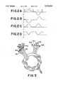
- FIGS. 2A-2Dare graphs of electrical signals illustrating a signal conversion process performed by the receiver section of FIG. 1A;
- FIG. 3is a perspective view of the windings of an inductive device used in the receiver section of FIG. 1A;
- FIG. 4is a schematic diagram of a transmitter section of an embodiment of the high speed data transceiver according to the present invention.
- FIGS. 5A-5Dare graphs of electrical signals illustrating a signal conversion process performed by the transmitter section of FIG. 4.
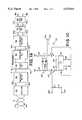
- FIG. 1Athere is shown a block diagram of a receiver circuit 9 for receiving a data signal from a conductive cable 10 and producing a converted data signal having a desired logic level at terminals 92a and 92b.
- the conductive cable 10is an unshielded twisted pair cable comprising two intertwined conductors 10a and 10b, although other types of cables such as coaxial or STP can be used.
- the data signal carried on the conductive cable 10is preferably a pseudoternary line-coded signal having a peak-to-peak voltage on the order of 2 Volts.
- An isolation stage 20 of the receiver 9includes a transformer for isolating the receiver 9 from the cable 10. The isolation stage 20 provides an isolated signal at terminals 26a and 26b.
- An impedance-matching network 30is connected across terminals 26a and 26b in order to match the effective load impedance of the receiver 9 to the impedance of the conductive cable 10 and thereby provide maximum power transfer to the receiver 9 and prevent reflection of the received signal.
- the impedance-matching network 30provides the input signal to an equalizing network 45.
- the equalizing network 45preferably includes a fixed equalizer 40 which provides partial compensation for distortion of the received signal that may be present due to transmission of the signal via conductive cable 10.
- the equalizing network 45does not necessarily provide complete equalization of the received signal. For example, if a broad spectrum signal is fully equalized using only passive components, the resulting relative attenuation of the lower frequencies would be too large to permit efficient rectification of the differential signal.
- the equalizing network 45includes two fixed, single-pole filters that are each connected in series with respective terminals 26a and 26b.
- a non-linear, or switched equalization network 50may be utilized within the equalizing network 45 in order to eliminate undesirable overcompensation.
- the non-linear equalization networkprovides attenuation of high frequencies in a manner that is dependent upon the amplitude of the received signal.
- the equalizing network 45provides an equalized multi-level signal to a differential decoder 60 via terminals 42a and 42b.
- the differential decoder 60converts the multi-level signal into a differential binary signal.
- the differential decoder 60includes a differential switching network which provides effective differential rectification of a multi-level signal, such as a pseudoternary signal.
- the differential decoder 60provides a differential binary signal at terminals 62a and 62b.
- a second equalizer 70is connected with terminals 62a and 62b to provide additional compensation for signal distortion.
- the second equalizing network 70provides enhanced equalization of the signal present at terminals 62a and 62b in order to accentuate the high frequency components of the differential binary signal relative to the lower frequencies at a ratio beyond that which would be practical prior to rectification as has been discussed herein in connection with the equalizing network 45.
- the equalized differential binary signal at terminals 72a and 72b of the second equalizing network 70is input to a logic level conversion stage 90.
- the logic level conversion stageconverts the differential binary signal into a desired logic level for the computing device which is to receive the data.
- the isolation stage 20includes a pair of longitudinal chokes 12 and 14 having terminals attached in series to conductors 10a and 10b respectively.
- the other terminals of longitudinal chokes 12 and 14are connected to respective primary terminals of a transformer 22.
- the longitudinal chokes 12 and 14 in combination with the transformer 22serve to isolate subsequent stages of the receiver 9 from common mode components of the signal present on the conductive cable 10.
- each of the longitudinal chokes 12 and 14has an inductance of 20 ⁇ H and the transformer 22 has a turns ratio of 1:1.
- transformer 22has a primary center tap connected to ground through a capacitor C1. Protection against surge signals, such as electrostatic discharges, is provided in the form of a threshold voltage conduction device 24 connected in parallel with capacitor C1.
- the impedance-matching stage and the fixed equalization stage of the receiver 9are provided by a passive network which includes an inductor L1 connected in series with a resistor R1 across terminals 26a and 26b, a resistor R2 in parallel with a capacitor C2 connected in series with terminal 26a, and a resistor R2' in parallel with a capacitor C2' connected in series with terminal 26b.
- the effective time constants of the combined impedance matching and fixed equalization stageare also influenced by a bias network discussed in further detail hereinafter and including resistors R3 and R3' connected in series across terminals 26a and 26b, a resistor R4 connected between Vcc and the common connection of resistors R3 and R3', a resistor R5 connected between ground and the common connection of resistors R3 and R3' and a capacitor C4 connected in parallel with resistor R5.
- L1is a 100 nH inductor and R1 is a 75 ⁇ resistor.
- the combination of L1 and R1provides a high-pass filter which serves to attenuate low frequency components of the received signal. Additional high-pass filtering is performed upon the signal present at terminals 26a and 26b by the combinations of R2 and C2, and by R2' and C2' respectively.
- R2 and R2'may be 200 ⁇ resistors and C2 and C2' may be 130 pF capacitors. Other values may be selected as desired for the particular application for which the receiver 9 is employed.
- These filtersprovide a partially equalized signal upon terminals 42a and 42b.
- Terminals 42a and 42bare connected to the differential decoder stage 60, which is embodied as a differential full-wave rectifier.
- the differential decoder 60effectively converts the differential pseudoternary signals at terminals 42a and 42b into differential binary signals which are provided terminals 62a and 62b of the differential decoder 60. The effect of this conversion is illustrated in FIGS. 2A-2D.
- FIG. 2Athere is shown a representative pseudoternary waveform for the sequence ⁇ 0,1,0,-1,0 ⁇ as may be present terminal 42a.
- the designation ⁇ 0,1,0,-1,0 ⁇is used for explanatory purposes.
- the actual serial data represented by the signal shown in FIG. 2Amay be other than the digits 0,1,0,-1,0 depending on the type of line coding employed.
- FIG. 2Bshows the corresponding waveform at terminal 42b.
- the differential binary output waveforms provided by differential decoder 60 at terminals 62a and 62bare shown in respective FIGS. 2C and 2D.
- the waveform at terminal 62aexhibits transitions from ground to Vcc upon each 0-to-1 transition of the differential pseudoternary signal.
- the waveform terminal 62bexhibits complementary transitions from Vcc to ground upon each 0-to-1 transition of the differential pseudoternary signal.
- the waveforms present at terminals 62a and 62bconstitute a differential binary signal that is confined between Vcc and ground.
- the differential decoder 60includes a switching network comprising two complementary pairs of bipolar junction transistors, NPN transistors Q1 and Q2, and PNP transistors Q3 and Q4.
- Terminal 42ais connected with the base of NPN transistor Q2 and with the base of PNP transistor Q3.
- Terminal 42bis connected with the base of NPN transistor Q1 and with the base of PNP transistor Q4.
- the collectors of NPN transistors Q1 and Q2are both connected to Vcc.
- the emitters of NPN transistors Q1 and Q2are connected to ground via resistor R6 which may be a 1 K ⁇ resistor.
- the voltage signal upon terminal 62aincreases whenever the forward bias of the emitter-base junctions of either Q1 or Q2 increases.
- the emitters of PNP transistors Q3 and Q4are connected to Vcc via resistor R7 which may be a 1 K ⁇ resistor.
- the collectors of PNP transistors Q3 and Q4are grounded. It can be seen that the voltage at terminal 62b will decrease whenever the forward bias of the emitter-base junctions of either Q3 or Q4 increases. Such an increase in bias occurs whenever the voltage at terminal 42a decreases or whenever the voltage at terminal 42b decreases. Thus, the resulting voltage at terminal 62b will respond negatively to both the positive and negative excursions of the pseudoternary signal as described in connection with FIGS. 2A-2D.
- the decoder stage 60is effective to convert pseudoternary signal into a differential binary signal.
- each decoder stageis effective to convert a 2N-1 level signal to a 2N-3 level signal with the final stage of the cascade providing a differential binary signal.
- a bias networkis incorporated into the first equalizing network 45 for providing an appropriate DC bias to the transistors Q1-Q4.
- the bias networkincludes two resistors R3, R3' in series across terminals 42a and 42b.
- the common connection of resistors R3, R3'is connected to Vcc via resistor R4 and to ground via resistor RS.
- Preferred values for these resistorsare 100 ⁇ for R3 and R3', and 510 ⁇ each for R4 and RS.
- a decoupling capacitor C2such as a 0.1 ⁇ F capacitor, is provided in parallel with resistor R5 in order to provide a ground path for stray transient signals.
- the DC bias applied to the bases of transistors Q1-Q4is determined by the entire DC equivalent presented to the bases of the transistors Q1-Q4.
- the value of resistors R2, R2'may be chosen according to the desired time constant of the fixed equalizer 40 and the desired transistor bias voltage.
- the values of resistors R3, R3 'also influence the transfer characteristic of the small-signal equivalent circuit presented to the secondary terminals of the transformer 22.
- the differential binary signal at terminals 62a and 62bis input to the second equalizing network 70 via a pair of DC-blocking capacitors C5, C5' in series with respective terminals 62a and 62b.
- the capacitors C5, C5'preferably 0.1 ⁇ F each, isolate the second equalizing network 70 from any DC voltage levels present at the emitters of transistors Q1-Q4 and pass the differential binary signal.
- the second equalizing network 70preferably includes two fixed, single-pole filters that are each connected in series with the respective DC-blocking capacitors C5, C5'.
- Each of the filters in equalizing network 70includes a resistor R8 in parallel with a capacitor C6 and a pair of resistors R9 and R9' connected in series across terminals 72a and 72b of the second equalizing network.
- R8is a 510 ⁇ resistor
- C2is a 15 pF capacitor
- R9 and R9'are 200 ⁇ resistors.
- a logic level conversion stage 90includes a limiting differential amplifier suitable for providing a binary signal compatible with ECL (emitter-coupled logic) circuitry.
- the limiting differential amplifieris preferably constructed using cascaded stages of a Motorola MC10116 Triple Line Receiver integrated circuit.
- the resistors R9, R9'may be provided with a bias adjust terminal Vbb at the common connection thereof to provide a DC bias if such a bias is required by the differential amplifier in logic level conversion stage 90.
- the receiver circuit 9is preferably provided with an additional equalizing filter having a non-linear equalization characteristic relative to the signal amplitude at terminals 42a and 42b.
- the nonlinear equalizer 50includes a pair of threshold voltage conduction devices such as Schottky diodes D1 and D2 which are connected in parallel with opposing polarities. The parallel combination of diodes is connected in series with a capacitor C3 which is preferably a 35 pF capacitor.
- the effect of this arrangementis to provide low pass filtering of the signal upon terminals 42a and 42b whenever the transient voltage between terminals 42a and 42b exceeds the threshold voltage of one of the diodes D1 or D2.
- the non-linear equalization network 50may alternatively employ field-effect transistors or other non-linear switching devices to achieve a similar result.
- the equalization network 45'provides amplification as well as equalization of the signal at terminals 26a and 26b.
- a pair of NPN transistors Q5 and Q6are configured as a differential amplifier each having a two-pole filter connected within in their respective emitter bias circuits.
- Terminal 26ais connected with the base of transistor Q5 and terminal 26b is connected with the base of transistor Q6 in order to provide differential equalization and amplification of the signals received on each of terminals 26a and 26b.
- the equalizer 45'may also include a non-linear, or switched, equalization capability in the form of filter 50' which operates similarly to filter 50 described in connection with FIG. 1B.
- the transformer coreis a toroid having an outer diameter of 0.155" and an inner diameter of 0.087".
- the magnetic path length of the coreis preferably 0.97 cm with a cross-sectional area of 0.011 cm 2 and a relative permeability of about 7500.
- the primary wire 120includes terminals 120a and 120b.
- the primary wire 120is wound ten times upon the transformer core, connected to a center tap 120c, and then wound ten more times.
- the secondary wire 130which includes terminals 130a and 130b, is wound twenty times upon the transformer core to provide a turns ratio of 1:1.
- Isolation transformers used to couple digital signals into receiver circuit 9can be a source of undesirable electromagnetic emissions. Additionally, high-frequency capacitive coupling between the individual windings of the transformer can reduce the efficiency of the transformer.
- two shielding wires 150 and 140are wound upon the transformer cores as follows.
- the shielding wire 150is wound upon the transformer core adjacent to the windings of the primary wire 120 so that each turn of the primary wire 120 is adjacent to respective turns of the shielding wire 150.
- the shielding wire 140is wound upon the transformer core adjacent to the windings of the secondary wire 130 so that each turn of the secondary wire 130 is adjacent to respective turns of the shielding wire 140.
- the primary terminals 120a and 120bare connected with the incoming data signal cable and the secondary terminals 130a and 130b are connected within the receiver circuit as described in connection with FIG. 1B.
- the terminals 140a and 140b of the shielding wire 140 and the terminals 150a and 150b of the shielding wire 150are all connected to ground.
- the grounded shielding wires 140 and 150serve to confine electromagnetic fields within the transformer 112 that would otherwise contribute to electromagnetic emissions or capacitive coupling between turns of the primary or secondary coils.
- a control winding 160including terminals 160a and 160b, may be wound upon the core as shown.
- the control winding 160allows a DC restoration circuit to apply sufficient current to the winding 160 in order to counteract the effects of undesirable DC levels within the secondary winding 130.
- the isolation stage 20includes a DC restoration circuit 165.
- the DC restoration circuit 165may include an averaging amplifier, or signal detection circuit, connected with one of the signal-carrying conductors of the receiver circuit in order to modulate the control winding current in accordance with the average DC level of the detected signal.
- the resistors R10, R10'are preferably relatively large, such as 10K ⁇ , so that the DC restoration circuit does not load the impedance-matching and equalization network.
- the capacitors C8, C8'may be 0.1 ⁇ F capacitor for storing the average signal level for a sufficient period of time.
- the resistors R11 and R13serve to set the gain of the DC restoration circuit so that the correction current is of a suitable magnitude depending upon the characteristics of the transformer 22 and the control winding 160. A gain on the order of 10 has been found to be sufficient for the signal values and transformer characteristics described herein.
- a current limiting resistor R14such as a 510 ⁇ resistor, determines the range of current that will be applied to the control winding.
- the receiver circuit of the present inventionis preferably packaged together with a transmitter circuit in order to provide a transceiver module that is capable of not only receiving, but also transmitting differential pseudoternary signals.
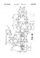
- a suitable transmitter circuit 11is shown in FIG. 4.
- the transmitting circuitreceives a binary logic signal at terminals 202a and 202b and generates a differential pseudoternary for transmission over a metallic conductive medium 260, e.g., a UTP cable.
- Terminals 202a and 202bare connected to the inputs of a buffer amplifier 210 having an inverting output and a non-inverting output.
- the buffer amplifier 210converts the binary input signal into a differential binary signal which is then provided to a conversion circuit over conductors 212a and 212b.
- the conversion circuit 220includes two toggle circuits 222a and 222b, which are preferably Motorola 74AC74 positive-edge-triggered D-type latches.
- Conductor 212ais connected with the clock input of toggle circuit 222a.
- Conductor 212bis connected with the clock input of toggle circuit 222b.
- the inverted outputs of the toggle circuitsare connected with the respective D-inputs so that the toggle circuits will each produce a logic level transition whenever a low to high transition is applied to the respective clock inputs.
- each toggle circuitis connected with conductor 224a via respective resistors R1' and R1", which are preferably 100 ⁇ resistors.
- the inverting outputs of toggle circuits 222a and 222 bare connected to conductor 224b via respective resistors R1' and R1" in a similar manner.
- the resistors R1' and R1"provide a mid-level voltage which is necessary to define a reference voltage for producing pseudoternary code. For example, the voltage level on conductor 224a will be at a low logic level whenever both non-inverting outputs of toggle circuits 222a and 222b are low.
- the voltage level at conductor 224awill be at a high logic level whenever the non-inverting outputs of toggle circuits 222a and 222b are high. Whenever the non-inverting outputs of the toggle circuits are at opposite logic levels, the resistors R1' and R1" provide a voltage divider that results in a mid-level voltage on conductor 224a. Successive transitions of the differential binary signal on conductors 212a and 212b cause the conversion circuit 220 to act as a threelevel sequential circuit.
- FIGS. 5A-5DThe operation of the conversion circuit 220 is illustrated in FIGS. 5A-5D.
- FIG. 5Ashows a waveform corresponding to the sequence 01010 on conductor 212a
- FIG. 5Bshows the corresponding complementary waveform on conductor 212b
- FIG. 5Cshows the resulting waveform on conductor 224a
- FIG. 5Dshows the resulting waveform on conductor 224b.
- the non-inverting output of toggle circuit 222ais low and the non-inverting output of toggle circuit 222b is high, hence the signals in FIGS. 5C and 5D are both at mid-level.
- the signal in FIG. 5Arepresenting the signal on conductor 212a, changes from low to high.
- toggle circuit 222aThe positive edge on the clock input of toggle circuit 222a causes toggle circuit 222a to latch its inverting output thus driving its non-inverting output high.
- the negative transition on conductor 212bcauses no change in the condition of toggle circuit 222b. Since the non-inverting outputs of the toggle circuits are both high at t l , the signal in FIG. 5C, representing the signal on conductor 224a is driven from mid-level to high.
- the signal in FIG. 5D, representing the signal on conductor 224bis driven low by the low condition of both of the inverting outputs of the toggle circuits.
- the voltage 5A on conductor 212amakes a high-to-low transition. This transition causes no change in the status of toggle circuit 222a.
- the corresponding upward transition of voltage 5B on conductor 212bcauses toggle circuit 222b to latch its low inverting output, thus driving the non-inverting output low and the inverting output high.
- the resultis that the voltages 5C and 5D are again driven to mid-level.
- the non-inverting output of toggle circuit 222ais driven low while the non-inverting output of toggle circuit 222b remains low.
- the conversion circuit 220provides a differential pseudoternary encoder wherein successive low-to-high transitions on conductor 212a result in alternating mid-to-high and mid-to-low transitions on conductor 224a with complementary transitions appearing on conductor 224b.
- conversion circuit 220Among the advantages of conversion circuit 220 relative to known binary-to-pseudoternary circuits is that the gate propagation delay from conductor 212a to conductors 224a and 224b is equal to the gate propagation delay from conductor and 212b to conductors 224a and 224b. Hence, the resulting pseudoternary signal exhibits superior transition symmetry and pulse width uniformity than known pseudoternary conversion circuits.
- the differential pseudoternary signal on conductors 224a and 224bis input to a filter network 230.
- Filter network 230includes a fixed three-pole filter for attenuating high harmonic components of the differential pseudoternary signal and for matching the output impedance of the transmitter circuit 11 to the impedance of the conductive medium 260. Such high harmonic components cause undesirable high-frequency electromagnetic emissions during data transmission.
- One pole of filter network 230is provided by a pair of RC filters connected in series across conductors 224a and 224b.
- the RC filtersare connected to Vcc at their common connection.
- the RC filterseach include a resistor R2, preferably having a value of 50 ⁇ and a capacitor C1, preferably having a value of 30 pF.
- Another pole of filter network 230includes a pair of inductors L1, Li', preferably having a value of 100 nH and connected in series with respective conductors 224a and 224b.
- a third poleis provided by a resistor R3, preferably having a value of 50 ⁇ , and a capacitor C2 having a value of 15 pF which are connected in series across terminals 232a and 232b.
- the filtered differential pseudoternary signalis provided at terminals 232a and 232b of filter network 230, and are in turn input to isolation transformer 240.
- the output terminals of isolation transformer 240are connected to series chokes 25a and 250b which are in turn connected to the metallic conductive medium 260.
- the structure and functions of the isolation transformer 240 and its associated surge protection and decoupling circuit, the series chokes 25a and 250b , and the conductive medium 260are substantially identical to the similar arrangement of components described in connection with the input stage of receiver 9 of FIG 1B.
Landscapes
- Engineering & Computer Science (AREA)
- Computer Networks & Wireless Communication (AREA)
- Signal Processing (AREA)
- Power Engineering (AREA)
- Physics & Mathematics (AREA)
- Spectroscopy & Molecular Physics (AREA)
- Dc Digital Transmission (AREA)
Abstract
Description
Claims (3)
Priority Applications (2)
| Application Number | Priority Date | Filing Date | Title |
|---|---|---|---|
| US08/089,973US5533054A (en) | 1993-07-09 | 1993-07-09 | Multi-level data transmitter |
| US08/417,239US5796781A (en) | 1993-07-09 | 1995-04-05 | Data receiver having bias restoration |
Applications Claiming Priority (1)
| Application Number | Priority Date | Filing Date | Title |
|---|---|---|---|
| US08/089,973US5533054A (en) | 1993-07-09 | 1993-07-09 | Multi-level data transmitter |
Related Child Applications (1)
| Application Number | Title | Priority Date | Filing Date |
|---|---|---|---|
| US08/417,239Continuation-In-PartUS5796781A (en) | 1993-07-09 | 1995-04-05 | Data receiver having bias restoration |
Publications (1)
| Publication Number | Publication Date |
|---|---|
| US5533054Atrue US5533054A (en) | 1996-07-02 |
Family
ID=22220471
Family Applications (1)
| Application Number | Title | Priority Date | Filing Date |
|---|---|---|---|
| US08/089,973Expired - Fee RelatedUS5533054A (en) | 1993-07-09 | 1993-07-09 | Multi-level data transmitter |
Country Status (1)
| Country | Link |
|---|---|
| US (1) | US5533054A (en) |
Cited By (77)
| Publication number | Priority date | Publication date | Assignee | Title |
|---|---|---|---|---|
| US5734682A (en)* | 1993-03-02 | 1998-03-31 | Lukac-Kuruc; Eric | Method for increasing transmission rate |
| WO1998037672A1 (en)* | 1997-02-21 | 1998-08-27 | Analog Devices, Inc. | Logic isolator with high transient immunity |
| US5912924A (en)* | 1996-08-15 | 1999-06-15 | Seeq Technology, Inc. | Bidirectional channels using common pins for transmit and receive paths |
| US6127839A (en)* | 1998-09-01 | 2000-10-03 | Micron Technology, Inc. | Method and apparatus for reducing induced switching transients |
| US6185190B1 (en) | 1996-09-25 | 2001-02-06 | Lsi Logic Corporation | Method and apparatus for using synthetic preamble signals to awaken repeater |
| US6210056B1 (en)* | 1997-12-15 | 2001-04-03 | Heidelberger Druckmaschinen Ag | Circuit arrangement for level conversion of binary signals in a control system for a printing-technology machine |
| US6262600B1 (en) | 2000-02-14 | 2001-07-17 | Analog Devices, Inc. | Isolator for transmitting logic signals across an isolation barrier |
| US6266545B1 (en) | 1998-10-21 | 2001-07-24 | Telefonaktiebolaget Lm Ericsson (Publ) | Transferring data in a fixed-site radio transceiver station by modulating power supply current |
| GB2360427A (en)* | 2000-03-14 | 2001-09-19 | Power X Ltd | Data transmission driver device |
| US20010054953A1 (en)* | 2000-04-14 | 2001-12-27 | Kline Paul A. | Digital communications utilizing medium voltage power distribution lines |
| US20020110311A1 (en)* | 2001-02-14 | 2002-08-15 | Kline Paul A. | Apparatus and method for providing a power line communication device for safe transmission of high-frequency, high-bandwidth signals over existing power distribution lines |
| US20020135236A1 (en)* | 1997-10-23 | 2002-09-26 | Haigh Geoffrey T. | Non-optical signal isolator |
| US20030042571A1 (en)* | 1997-10-23 | 2003-03-06 | Baoxing Chen | Chip-scale coils and isolators based thereon |
| US20030070126A1 (en)* | 2001-09-14 | 2003-04-10 | Werner Carl W. | Built-in self-testing of multilevel signal interfaces |
| US20030093713A1 (en)* | 2001-09-14 | 2003-05-15 | Werner Carl W. | Multilevel signal interface testing with binary test apparatus by emulation of multilevel signals |
| US6639947B1 (en) | 1999-12-28 | 2003-10-28 | Koninklijke Philips Electronics N.V. | EMI reduction for isolated bus systems |
| US6731688B1 (en)* | 1999-12-13 | 2004-05-04 | Intel Corporation | Speed signaling for data communications |
| US20040213358A1 (en)* | 1994-05-23 | 2004-10-28 | Samsung Electronics Co., Ltd. | Radio receiver for receiving both VSB and QAM digital HDTV signals |
| US6816499B1 (en)* | 1999-06-11 | 2004-11-09 | International Business Machines Corporation | High speed token ring port configuror |
| US20040240564A1 (en)* | 2001-08-31 | 2004-12-02 | Johann Amstutz | Method and device for single conductor local transmission of pcm signals without transformers |
| US20040239402A1 (en)* | 2003-05-26 | 2004-12-02 | Laurent Dulau | Device for controlling a voltage-controlled power switch |
| US20050057277A1 (en)* | 2003-04-30 | 2005-03-17 | Analog Devices, Inc. | Signal isolators using micro-transformer |
| RU2252490C2 (en)* | 2003-07-18 | 2005-05-20 | Открытое акционерное общество Арзамасское научно-производственное предприятие "ТЕМП-АВИА" (ОАО АНПП "ТЕМП-АВИА") | Device for transmitting electrically isolated control signals |
| US6933835B2 (en) | 2001-02-14 | 2005-08-23 | Current Technologies, Llc | Data communication over a power line |
| US6950567B2 (en) | 2001-02-14 | 2005-09-27 | Current Technologies, Llc | Method and apparatus for providing inductive coupling and decoupling of high-frequency, high-bandwidth data signals directly on and off of a high voltage power line |
| US20050243983A1 (en)* | 2004-05-01 | 2005-11-03 | Vetco Gray Controls Limited | Modems |
| US6965302B2 (en) | 2000-04-14 | 2005-11-15 | Current Technologies, Llc | Power line communication system and method of using the same |
| US6965303B2 (en) | 2002-12-10 | 2005-11-15 | Current Technologies, Llc | Power line communication system and method |
| US6977578B2 (en) | 2000-01-20 | 2005-12-20 | Current Technologies, Llc | Method of isolating data in a power line communications network |
| US6980091B2 (en) | 2002-12-10 | 2005-12-27 | Current Technologies, Llc | Power line communication system and method of operating the same |
| US6980090B2 (en) | 2002-12-10 | 2005-12-27 | Current Technologies, Llc | Device and method for coupling with electrical distribution network infrastructure to provide communications |
| US6980089B1 (en) | 2000-08-09 | 2005-12-27 | Current Technologies, Llc | Non-intrusive coupling to shielded power cable |
| US6982611B2 (en) | 2002-06-24 | 2006-01-03 | Current Technologies, Llc | Power line coupling device and method of using the same |
| US6998962B2 (en) | 2000-04-14 | 2006-02-14 | Current Technologies, Llc | Power line communication apparatus and method of using the same |
| US7046124B2 (en) | 2003-01-21 | 2006-05-16 | Current Technologies, Llc | Power line coupling device and method of using the same |
| US7053756B2 (en) | 2001-12-21 | 2006-05-30 | Current Technologies, Llc | Facilitating communication of data signals on electric power systems |
| US7064654B2 (en) | 2002-12-10 | 2006-06-20 | Current Technologies, Llc | Power line communication system and method of operating the same |
| US7075414B2 (en) | 2003-05-13 | 2006-07-11 | Current Technologies, Llc | Device and method for communicating data signals through multiple power line conductors |
| US7076378B1 (en) | 2002-11-13 | 2006-07-11 | Current Technologies, Llc | Device and method for providing power line characteristics and diagnostics |
| US7102478B2 (en) | 2002-06-21 | 2006-09-05 | Current Technologies, Llc | Power line coupling device and method of using the same |
| US7113134B1 (en) | 2004-03-12 | 2006-09-26 | Current Technologies, Llc | Transformer antenna device and method of using the same |
| US7132819B1 (en) | 2002-11-12 | 2006-11-07 | Current Technologies, Llc | Floating power supply and method of using the same |
| US7199699B1 (en) | 2002-02-19 | 2007-04-03 | Current Technologies, Llc | Facilitating communication with power line communication devices |
| US20070216377A1 (en)* | 2006-03-16 | 2007-09-20 | Fuji Electric Device Technology Co., Ltd. | Power electronics equipments |
| US20070218595A1 (en)* | 2006-03-16 | 2007-09-20 | Fuji Electric Device Technology Co., Ltd. | Power electronics equipments |
| US7308103B2 (en) | 2003-05-08 | 2007-12-11 | Current Technologies, Llc | Power line communication device and method of using the same |
| US20080013635A1 (en)* | 2004-06-03 | 2008-01-17 | Silicon Laboratories Inc. | Transformer coils for providing voltage isolation |
| US20080025450A1 (en)* | 2004-06-03 | 2008-01-31 | Silicon Laboratories Inc. | Multiplexed rf isolator circuit |
| US20080031286A1 (en)* | 2004-06-03 | 2008-02-07 | Silicon Laboratories Inc. | Multiplexed rf isolator |
| US20080136442A1 (en)* | 2006-07-06 | 2008-06-12 | Baoxing Chen | Signal isolator using micro-transformers |
| US20080267301A1 (en)* | 2004-06-03 | 2008-10-30 | Silicon Laboratories Inc. | Bidirectional multiplexed rf isolator |
| US7447492B2 (en) | 2004-06-03 | 2008-11-04 | Silicon Laboratories Inc. | On chip transformer isolator |
| US7460604B2 (en) | 2004-06-03 | 2008-12-02 | Silicon Laboratories Inc. | RF isolator for isolating voltage sensing and gate drivers |
| US7460467B1 (en) | 2003-07-23 | 2008-12-02 | Current Technologies, Llc | Voice-over-IP network test device and method |
| US20080317106A1 (en)* | 2004-06-03 | 2008-12-25 | Silicon Laboratories Inc. | Mcu with integrated voltage isolator and integrated galvanically isolated asynchronous serial data link |
| US20090017773A1 (en)* | 2004-06-03 | 2009-01-15 | Silicon Laboratories Inc. | Capacitive isolator |
| US7499489B1 (en)* | 2004-09-16 | 2009-03-03 | Analog Devices, Inc. | Equalization in clock recovery receivers |
| US20090129178A1 (en)* | 1997-10-10 | 2009-05-21 | Barth Richard M | Integrated Circuit Memory Device Having Delayed Write Timing Based on Read Response Time |
| US20090213914A1 (en)* | 2004-06-03 | 2009-08-27 | Silicon Laboratories Inc. | Capacitive isolation circuitry |
| US7737871B2 (en) | 2004-06-03 | 2010-06-15 | Silicon Laboratories Inc. | MCU with integrated voltage isolator to provide a galvanic isolation between input and output |
| US7902627B2 (en) | 2004-06-03 | 2011-03-08 | Silicon Laboratories Inc. | Capacitive isolation circuitry with improved common mode detector |
| US7961050B1 (en)* | 2010-02-17 | 2011-06-14 | Taiwan Semiconductor Manufacturing Company, Ltd. | Integrated circuits including an equalizer and operating methods thereof |
| CN102176672A (en)* | 2011-03-18 | 2011-09-07 | 电子科技大学 | Level shifting circuit |
| US8265129B1 (en)* | 1994-06-28 | 2012-09-11 | Samsung Electronics Co., Ltd. | Digital receiver with system for controlling the operating mode of an adaptive equalizer |
| US8441325B2 (en) | 2004-06-03 | 2013-05-14 | Silicon Laboratories Inc. | Isolator with complementary configurable memory |
| US8451032B2 (en) | 2010-12-22 | 2013-05-28 | Silicon Laboratories Inc. | Capacitive isolator with schmitt trigger |
| US8570074B2 (en)* | 2008-08-12 | 2013-10-29 | Marvell International Ltd. | Method and apparatus for reducing transmitter AC-coupling droop |
| TWI514780B (en)* | 2014-07-08 | 2015-12-21 | Ncku Res & Dev Foundation | Duobinary voltage-mode transmitter |
| US9293997B2 (en) | 2013-03-14 | 2016-03-22 | Analog Devices Global | Isolated error amplifier for isolated power supplies |
| US9660848B2 (en) | 2014-09-15 | 2017-05-23 | Analog Devices Global | Methods and structures to generate on/off keyed carrier signals for signal isolators |
| US9998301B2 (en) | 2014-11-03 | 2018-06-12 | Analog Devices, Inc. | Signal isolator system with protection for common mode transients |
| US10270630B2 (en) | 2014-09-15 | 2019-04-23 | Analog Devices, Inc. | Demodulation of on-off-key modulated signals in signal isolator systems |
| US10290608B2 (en) | 2016-09-13 | 2019-05-14 | Allegro Microsystems, Llc | Signal isolator having bidirectional diagnostic signal exchange |
| US10419251B2 (en) | 2002-09-18 | 2019-09-17 | Infineon Technologies | Digital signal transfer using integrated transformers with electrical isolation |
| US10536309B2 (en) | 2014-09-15 | 2020-01-14 | Analog Devices, Inc. | Demodulation of on-off-key modulated signals in signal isolator systems |
| US10985954B1 (en) | 2019-11-05 | 2021-04-20 | Samsung Electronics Co., Ltd. | Data transmission devices with efficient ternary-based data transmission capability and methods of operating same |
| US11115244B2 (en) | 2019-09-17 | 2021-09-07 | Allegro Microsystems, Llc | Signal isolator with three state data transmission |
Citations (14)
| Publication number | Priority date | Publication date | Assignee | Title |
|---|---|---|---|---|
| US3649751A (en)* | 1970-01-23 | 1972-03-14 | Stewart Warner Corp | Compressed bandwidth transmission sysem |
| US3866147A (en)* | 1973-02-26 | 1975-02-11 | Univ Sherbrooke | Balanced correlated ternary coding system |
| US3988676A (en)* | 1971-05-17 | 1976-10-26 | Milgo Electronic Corporation | Coding and decoding system with multi-level format |
| US3993953A (en)* | 1975-10-17 | 1976-11-23 | Gte Automatic Electric Laboratories Incorporated | Apparatus and method for digitally generating a modified duobinary signal |
| US4084069A (en)* | 1976-11-01 | 1978-04-11 | Burroughs Corporation | Encoding and driving means for use in a three-level digital data communication system |
| US4086587A (en)* | 1977-02-28 | 1978-04-25 | Gte Automatic Electric Laboratories Incorporated | Apparatus and method for generating a high-accuracy 7-level correlative signal |
| US4468787A (en)* | 1981-11-09 | 1984-08-28 | Lear Siegler, Inc. | Ternary data transmission system |
| US4717896A (en)* | 1985-03-21 | 1988-01-05 | And Yet, Inc. | Balun |
| EP0299639A2 (en)* | 1987-07-13 | 1989-01-18 | David Systems, Inc. | Digital data communications system |
| US4821295A (en)* | 1987-11-30 | 1989-04-11 | Tandem Computers Incorporated | Two-stage synchronizer |
| US4897854A (en)* | 1989-02-24 | 1990-01-30 | General Instrument Corporation | Alternate pulse inversion encoding scheme for serial data transmission |
| US5113159A (en)* | 1990-02-22 | 1992-05-12 | At&T Bell Laboratories | Communications transmission system including facilities for suppressing electromagnetic interference |
| US5173618A (en)* | 1990-05-14 | 1992-12-22 | Vlsi Technology, Inc. | Clock generator for providing a pair of nonoverlapping clock signals with adjustable skew |
| US5280500A (en)* | 1991-10-10 | 1994-01-18 | Crescendo Communications, Inc. | Method and apparatus for multilevel encoding for a local area network |
- 1993
- 1993-07-09USUS08/089,973patent/US5533054A/ennot_activeExpired - Fee Related
Patent Citations (14)
| Publication number | Priority date | Publication date | Assignee | Title |
|---|---|---|---|---|
| US3649751A (en)* | 1970-01-23 | 1972-03-14 | Stewart Warner Corp | Compressed bandwidth transmission sysem |
| US3988676A (en)* | 1971-05-17 | 1976-10-26 | Milgo Electronic Corporation | Coding and decoding system with multi-level format |
| US3866147A (en)* | 1973-02-26 | 1975-02-11 | Univ Sherbrooke | Balanced correlated ternary coding system |
| US3993953A (en)* | 1975-10-17 | 1976-11-23 | Gte Automatic Electric Laboratories Incorporated | Apparatus and method for digitally generating a modified duobinary signal |
| US4084069A (en)* | 1976-11-01 | 1978-04-11 | Burroughs Corporation | Encoding and driving means for use in a three-level digital data communication system |
| US4086587A (en)* | 1977-02-28 | 1978-04-25 | Gte Automatic Electric Laboratories Incorporated | Apparatus and method for generating a high-accuracy 7-level correlative signal |
| US4468787A (en)* | 1981-11-09 | 1984-08-28 | Lear Siegler, Inc. | Ternary data transmission system |
| US4717896A (en)* | 1985-03-21 | 1988-01-05 | And Yet, Inc. | Balun |
| EP0299639A2 (en)* | 1987-07-13 | 1989-01-18 | David Systems, Inc. | Digital data communications system |
| US4821295A (en)* | 1987-11-30 | 1989-04-11 | Tandem Computers Incorporated | Two-stage synchronizer |
| US4897854A (en)* | 1989-02-24 | 1990-01-30 | General Instrument Corporation | Alternate pulse inversion encoding scheme for serial data transmission |
| US5113159A (en)* | 1990-02-22 | 1992-05-12 | At&T Bell Laboratories | Communications transmission system including facilities for suppressing electromagnetic interference |
| US5173618A (en)* | 1990-05-14 | 1992-12-22 | Vlsi Technology, Inc. | Clock generator for providing a pair of nonoverlapping clock signals with adjustable skew |
| US5280500A (en)* | 1991-10-10 | 1994-01-18 | Crescendo Communications, Inc. | Method and apparatus for multilevel encoding for a local area network |
Non-Patent Citations (16)
| Title |
|---|
| Banwell, T. C., "Bit Error Characteristics of Correlated Three Level Coding", ANSI X3T9.5 TP-PMD working group document #TP-PMD-146, Oct. 14, 1992, 6 sheets. |
| Banwell, T. C., Bit Error Characteristics of Correlated Three Level Coding , ANSI X3T9.5 TP PMD working group document TP PMD 146, Oct. 14, 1992, 6 sheets.* |
| Banwell, T. C., MLT 3, vs. NRZ1 Testing results, ANSI X3T9.5 TP PMD working group document TP PMD 181, Jun. 24, 1992, 6 sheets.* |
| Banwell, T. C., MLT-3, vs. NRZ1 Testing results, ANSI X3T9.5 TP-PMD working group document #TP-PMD-181, Jun. 24, 1992, 6 sheets. |
| Eugen Gerthon, FDDI on Copper With AMD PHY Components, Advanced Micro Devices, 1991, 8 sheets.* |
| IBM Technical Disclosure Bulletin, vol. 6, No. 9, Feb. 1964.* |
| Mazzola, Mario, "A Proposal for a Low-Cost FDDI UTP/ STP PMD Standard", ANSI X3T9. TP-PMD working group document #TP-PMD-078, Oct. 15, 1991, 32 sheets. |
| Mazzola, Mario, "Implementation Issues in an MLT-3 Based TP-PMD", ANSI X3T9.5 TP-PMD working group document #TP-PMD-128, Apr. 29, 1992, 17 sheets. |
| Mazzola, Mario, A Proposal for a Low Cost FDDI UTP/ STP PMD Standard , ANSI X3T9. TP PMD working group document TP PMD 078, Oct. 15, 1991, 32 sheets.* |
| Mazzola, Mario, Crescendo Communications MLT 3 Receiver Circuit Diagram, ANSI X3T9, T PMD working group document TP PMD 162, Jun. 8, 1992, 2 sheets.* |
| Mazzola, Mario, Crescendo Communications MLT-3 Receiver Circuit Diagram, ANSI X3T9, T-PMD working group document #TP-PMD-162, Jun. 8, 1992, 2 sheets. |
| Mazzola, Mario, Implementation Issues in an MLT 3 Based TP PMD , ANSI X3T9.5 TP PMD working group document TP PMD 128, Apr. 29, 1992, 17 sheets.* |
| Synoptics Corp., "FDDI--UTP--Investigation", ANSI X3T9.5 TP-PMD working group document #TP-PMD-084, Oct. 5, 1991, 6 sheets. |
| Synoptics Corp., FDDI UTP Investigation , ANSI X3T9.5 TP PMD working group document TP PMD 084, Oct. 5, 1991, 6 sheets.* |
| The X3T9.5 Copper FDDI Station, Advanced Micro Devices, pp. 3 4, A 6, A 7.* |
| The X3T9.5 Copper FDDI Station, Advanced Micro Devices, pp. 3-4, A-6, A-7. |
Cited By (136)
| Publication number | Priority date | Publication date | Assignee | Title |
|---|---|---|---|---|
| US5734682A (en)* | 1993-03-02 | 1998-03-31 | Lukac-Kuruc; Eric | Method for increasing transmission rate |
| US20040213358A1 (en)* | 1994-05-23 | 2004-10-28 | Samsung Electronics Co., Ltd. | Radio receiver for receiving both VSB and QAM digital HDTV signals |
| US8265129B1 (en)* | 1994-06-28 | 2012-09-11 | Samsung Electronics Co., Ltd. | Digital receiver with system for controlling the operating mode of an adaptive equalizer |
| US5912924A (en)* | 1996-08-15 | 1999-06-15 | Seeq Technology, Inc. | Bidirectional channels using common pins for transmit and receive paths |
| US6327309B1 (en) | 1996-08-15 | 2001-12-04 | Lsi Logic Corporation | Bidirection channels using common pins for transmit and receive paths |
| US6185190B1 (en) | 1996-09-25 | 2001-02-06 | Lsi Logic Corporation | Method and apparatus for using synthetic preamble signals to awaken repeater |
| WO1998037672A1 (en)* | 1997-02-21 | 1998-08-27 | Analog Devices, Inc. | Logic isolator with high transient immunity |
| US5952849A (en)* | 1997-02-21 | 1999-09-14 | Analog Devices, Inc. | Logic isolator with high transient immunity |
| US20090129178A1 (en)* | 1997-10-10 | 2009-05-21 | Barth Richard M | Integrated Circuit Memory Device Having Delayed Write Timing Based on Read Response Time |
| US7793039B2 (en) | 1997-10-10 | 2010-09-07 | Rambus Inc. | Interface for a semiconductor memory device and method for controlling the interface |
| US8019958B2 (en) | 1997-10-10 | 2011-09-13 | Rambus Inc. | Memory write signaling and methods thereof |
| US8205056B2 (en) | 1997-10-10 | 2012-06-19 | Rambus Inc. | Memory controller for controlling write signaling |
| US8560797B2 (en) | 1997-10-10 | 2013-10-15 | Rambus Inc. | Method and apparatus for indicating mask information |
| US7545059B2 (en) | 1997-10-23 | 2009-06-09 | Analog Devices, Inc. | Chip-scale coils and isolators based thereon |
| US20080030080A1 (en)* | 1997-10-23 | 2008-02-07 | Baoxing Chen | Chip-scale coils and isolators based thereon |
| US6873065B2 (en) | 1997-10-23 | 2005-03-29 | Analog Devices, Inc. | Non-optical signal isolator |
| US20020135236A1 (en)* | 1997-10-23 | 2002-09-26 | Haigh Geoffrey T. | Non-optical signal isolator |
| US20030042571A1 (en)* | 1997-10-23 | 2003-03-06 | Baoxing Chen | Chip-scale coils and isolators based thereon |
| US6210056B1 (en)* | 1997-12-15 | 2001-04-03 | Heidelberger Druckmaschinen Ag | Circuit arrangement for level conversion of binary signals in a control system for a printing-technology machine |
| US6359463B2 (en)* | 1998-09-01 | 2002-03-19 | Micron Technology, Inc. | Method and apparatus for reducing induced switching transients |
| US6359462B1 (en) | 1998-09-01 | 2002-03-19 | Micron Technology, Inc | Method and apparatus for reducing induced switching transients |
| US6127839A (en)* | 1998-09-01 | 2000-10-03 | Micron Technology, Inc. | Method and apparatus for reducing induced switching transients |
| US6266545B1 (en) | 1998-10-21 | 2001-07-24 | Telefonaktiebolaget Lm Ericsson (Publ) | Transferring data in a fixed-site radio transceiver station by modulating power supply current |
| US6816499B1 (en)* | 1999-06-11 | 2004-11-09 | International Business Machines Corporation | High speed token ring port configuror |
| US6731688B1 (en)* | 1999-12-13 | 2004-05-04 | Intel Corporation | Speed signaling for data communications |
| US6639947B1 (en) | 1999-12-28 | 2003-10-28 | Koninklijke Philips Electronics N.V. | EMI reduction for isolated bus systems |
| US6977578B2 (en) | 2000-01-20 | 2005-12-20 | Current Technologies, Llc | Method of isolating data in a power line communications network |
| US20030128053A1 (en)* | 2000-02-14 | 2003-07-10 | Analog Devices, Inc. | Logic isolator for transmitting periodic signals across an isolation barrier |
| US6262600B1 (en) | 2000-02-14 | 2001-07-17 | Analog Devices, Inc. | Isolator for transmitting logic signals across an isolation barrier |
| US20040207431A1 (en)* | 2000-02-14 | 2004-10-21 | Analog Devices, Inc. | Logic isolator |
| US6525566B2 (en) | 2000-02-14 | 2003-02-25 | Analog Devices, Inc. | Isolator for transmitting logic signals across an isolation barrier |
| US6903578B2 (en) | 2000-02-14 | 2005-06-07 | Analog Devices, Inc. | Logic isolator |
| US20010024477A1 (en)* | 2000-03-14 | 2001-09-27 | Power X Limited | Method for controlling a data transmission pre-emphasis unit and a data transmission system employing the method |
| GB2360427B (en)* | 2000-03-14 | 2004-02-04 | Power X Ltd | Data transmission driver device |
| US6704365B2 (en) | 2000-03-14 | 2004-03-09 | Xyratex Technology Limited | Data transmission driver device |
| US7006580B2 (en) | 2000-03-14 | 2006-02-28 | Xyratex Technology Limited | Method for controlling a data transmission pre-emphasis unit and a data transmission system employing the method |
| GB2360427A (en)* | 2000-03-14 | 2001-09-19 | Power X Ltd | Data transmission driver device |
| US7245212B2 (en) | 2000-04-14 | 2007-07-17 | Current Technologies, Llc | Power line communication apparatus and method of using the same |
| US20010054953A1 (en)* | 2000-04-14 | 2001-12-27 | Kline Paul A. | Digital communications utilizing medium voltage power distribution lines |
| US7307511B2 (en) | 2000-04-14 | 2007-12-11 | Current Technologies, Llc | Power line communication system and method |
| US6958680B2 (en) | 2000-04-14 | 2005-10-25 | Current Technologies, Llc | Power line communication system and method of using the same |
| US6965302B2 (en) | 2000-04-14 | 2005-11-15 | Current Technologies, Llc | Power line communication system and method of using the same |
| US6998962B2 (en) | 2000-04-14 | 2006-02-14 | Current Technologies, Llc | Power line communication apparatus and method of using the same |
| US6980089B1 (en) | 2000-08-09 | 2005-12-27 | Current Technologies, Llc | Non-intrusive coupling to shielded power cable |
| US7414518B2 (en) | 2001-02-14 | 2008-08-19 | Current Technologies, Llc | Power line communication device and method |
| US6933835B2 (en) | 2001-02-14 | 2005-08-23 | Current Technologies, Llc | Data communication over a power line |
| US7103240B2 (en) | 2001-02-14 | 2006-09-05 | Current Technologies, Llc | Method and apparatus for providing inductive coupling and decoupling of high-frequency, high-bandwidth data signals directly on and off of a high voltage power line |
| US7218219B2 (en) | 2001-02-14 | 2007-05-15 | Current Technologies, Llc | Data communication over a power line |
| US7453352B2 (en) | 2001-02-14 | 2008-11-18 | Current Technologies, Llc | Data communication over a power line |
| US7042351B2 (en) | 2001-02-14 | 2006-05-09 | Current Technologies, Llc | Data communication over a power line |
| US7046882B2 (en) | 2001-02-14 | 2006-05-16 | Current Technologies, Llc | Power line communication system and method |
| US20050213874A1 (en)* | 2001-02-14 | 2005-09-29 | Kline Paul A | Power line communication system and method |
| US20020110311A1 (en)* | 2001-02-14 | 2002-08-15 | Kline Paul A. | Apparatus and method for providing a power line communication device for safe transmission of high-frequency, high-bandwidth signals over existing power distribution lines |
| US6950567B2 (en) | 2001-02-14 | 2005-09-27 | Current Technologies, Llc | Method and apparatus for providing inductive coupling and decoupling of high-frequency, high-bandwidth data signals directly on and off of a high voltage power line |
| US20040240564A1 (en)* | 2001-08-31 | 2004-12-02 | Johann Amstutz | Method and device for single conductor local transmission of pcm signals without transformers |
| US20030093713A1 (en)* | 2001-09-14 | 2003-05-15 | Werner Carl W. | Multilevel signal interface testing with binary test apparatus by emulation of multilevel signals |
| US7162672B2 (en)* | 2001-09-14 | 2007-01-09 | Rambus Inc | Multilevel signal interface testing with binary test apparatus by emulation of multilevel signals |
| US20030070126A1 (en)* | 2001-09-14 | 2003-04-10 | Werner Carl W. | Built-in self-testing of multilevel signal interfaces |
| US20060242483A1 (en)* | 2001-09-14 | 2006-10-26 | Rambus Inc. | Built-in self-testing of multilevel signal interfaces |
| US7053756B2 (en) | 2001-12-21 | 2006-05-30 | Current Technologies, Llc | Facilitating communication of data signals on electric power systems |
| US7199699B1 (en) | 2002-02-19 | 2007-04-03 | Current Technologies, Llc | Facilitating communication with power line communication devices |
| US7102478B2 (en) | 2002-06-21 | 2006-09-05 | Current Technologies, Llc | Power line coupling device and method of using the same |
| US7224243B2 (en) | 2002-06-24 | 2007-05-29 | Current Technologies, Llc | Power line coupling device and method of using the same |
| US6982611B2 (en) | 2002-06-24 | 2006-01-03 | Current Technologies, Llc | Power line coupling device and method of using the same |
| US10419251B2 (en) | 2002-09-18 | 2019-09-17 | Infineon Technologies | Digital signal transfer using integrated transformers with electrical isolation |
| US7132819B1 (en) | 2002-11-12 | 2006-11-07 | Current Technologies, Llc | Floating power supply and method of using the same |
| US7076378B1 (en) | 2002-11-13 | 2006-07-11 | Current Technologies, Llc | Device and method for providing power line characteristics and diagnostics |
| US7701325B2 (en) | 2002-12-10 | 2010-04-20 | Current Technologies, Llc | Power line communication apparatus and method of using the same |
| US6965303B2 (en) | 2002-12-10 | 2005-11-15 | Current Technologies, Llc | Power line communication system and method |
| US7250848B2 (en) | 2002-12-10 | 2007-07-31 | Current Technologies, Llc | Power line communication apparatus and method of using the same |
| US6980091B2 (en) | 2002-12-10 | 2005-12-27 | Current Technologies, Llc | Power line communication system and method of operating the same |
| US6980090B2 (en) | 2002-12-10 | 2005-12-27 | Current Technologies, Llc | Device and method for coupling with electrical distribution network infrastructure to provide communications |
| US7301440B2 (en) | 2002-12-10 | 2007-11-27 | Current Technologies, Llc | Power line communication system and method |
| US7064654B2 (en) | 2002-12-10 | 2006-06-20 | Current Technologies, Llc | Power line communication system and method of operating the same |
| US7046124B2 (en) | 2003-01-21 | 2006-05-16 | Current Technologies, Llc | Power line coupling device and method of using the same |
| US20100134139A1 (en)* | 2003-04-30 | 2010-06-03 | Analog Devices, Inc. | Signal isolators using micro-transformers |
| US7920010B2 (en) | 2003-04-30 | 2011-04-05 | Analog Devices, Inc. | Signal isolators using micro-transformers |
| US7692444B2 (en) | 2003-04-30 | 2010-04-06 | Analog Devices, Inc. | Signal isolators using micro-transformers |
| US7075329B2 (en) | 2003-04-30 | 2006-07-11 | Analog Devices, Inc. | Signal isolators using micro-transformers |
| US8736343B2 (en) | 2003-04-30 | 2014-05-27 | Analog Devices, Inc. | Signal isolators using micro-transformers |
| US20080169834A1 (en)* | 2003-04-30 | 2008-07-17 | Baoxing Chen | Signal isolators using micro-transformers |
| US20060250155A1 (en)* | 2003-04-30 | 2006-11-09 | Baoxing Chen | Signal isolators using micro-transformers |
| US7683654B2 (en) | 2003-04-30 | 2010-03-23 | Analog Devices, Inc. | Signal isolators using micro-transformers |
| US20050057277A1 (en)* | 2003-04-30 | 2005-03-17 | Analog Devices, Inc. | Signal isolators using micro-transformer |
| US20110175642A1 (en)* | 2003-04-30 | 2011-07-21 | Analog Devices, Inc. | Signal isolators using micro-transformers |
| US7308103B2 (en) | 2003-05-08 | 2007-12-11 | Current Technologies, Llc | Power line communication device and method of using the same |
| US7075414B2 (en) | 2003-05-13 | 2006-07-11 | Current Technologies, Llc | Device and method for communicating data signals through multiple power line conductors |
| US6940319B2 (en)* | 2003-05-26 | 2005-09-06 | Stmicroelectronics S.A. | Device for controlling high and low levels of a voltage-controlled power switch |
| US20040239402A1 (en)* | 2003-05-26 | 2004-12-02 | Laurent Dulau | Device for controlling a voltage-controlled power switch |
| RU2252490C2 (en)* | 2003-07-18 | 2005-05-20 | Открытое акционерное общество Арзамасское научно-производственное предприятие "ТЕМП-АВИА" (ОАО АНПП "ТЕМП-АВИА") | Device for transmitting electrically isolated control signals |
| US7460467B1 (en) | 2003-07-23 | 2008-12-02 | Current Technologies, Llc | Voice-over-IP network test device and method |
| US7113134B1 (en) | 2004-03-12 | 2006-09-26 | Current Technologies, Llc | Transformer antenna device and method of using the same |
| US20050243983A1 (en)* | 2004-05-01 | 2005-11-03 | Vetco Gray Controls Limited | Modems |
| DE102005016986B4 (en) | 2004-05-01 | 2022-09-15 | Baker Hughes Energy Technology UK Limited | modem |
| US7856219B2 (en) | 2004-06-03 | 2010-12-21 | Silicon Laboratories Inc. | Transformer coils for providing voltage isolation |
| US8198951B2 (en) | 2004-06-03 | 2012-06-12 | Silicon Laboratories Inc. | Capacitive isolation circuitry |
| US20080013635A1 (en)* | 2004-06-03 | 2008-01-17 | Silicon Laboratories Inc. | Transformer coils for providing voltage isolation |
| US20090213914A1 (en)* | 2004-06-03 | 2009-08-27 | Silicon Laboratories Inc. | Capacitive isolation circuitry |
| US7577223B2 (en) | 2004-06-03 | 2009-08-18 | Silicon Laboratories Inc. | Multiplexed RF isolator circuit |
| US20080031286A1 (en)* | 2004-06-03 | 2008-02-07 | Silicon Laboratories Inc. | Multiplexed rf isolator |
| US20080267301A1 (en)* | 2004-06-03 | 2008-10-30 | Silicon Laboratories Inc. | Bidirectional multiplexed rf isolator |
| US7737871B2 (en) | 2004-06-03 | 2010-06-15 | Silicon Laboratories Inc. | MCU with integrated voltage isolator to provide a galvanic isolation between input and output |
| US7738568B2 (en) | 2004-06-03 | 2010-06-15 | Silicon Laboratories Inc. | Multiplexed RF isolator |
| US8441325B2 (en) | 2004-06-03 | 2013-05-14 | Silicon Laboratories Inc. | Isolator with complementary configurable memory |
| US7821428B2 (en) | 2004-06-03 | 2010-10-26 | Silicon Laboratories Inc. | MCU with integrated voltage isolator and integrated galvanically isolated asynchronous serial data link |
| US20080025450A1 (en)* | 2004-06-03 | 2008-01-31 | Silicon Laboratories Inc. | Multiplexed rf isolator circuit |
| US7902627B2 (en) | 2004-06-03 | 2011-03-08 | Silicon Laboratories Inc. | Capacitive isolation circuitry with improved common mode detector |
| US20090017773A1 (en)* | 2004-06-03 | 2009-01-15 | Silicon Laboratories Inc. | Capacitive isolator |
| US7447492B2 (en) | 2004-06-03 | 2008-11-04 | Silicon Laboratories Inc. | On chip transformer isolator |
| US20080317106A1 (en)* | 2004-06-03 | 2008-12-25 | Silicon Laboratories Inc. | Mcu with integrated voltage isolator and integrated galvanically isolated asynchronous serial data link |
| US7650130B2 (en) | 2004-06-03 | 2010-01-19 | Silicon Laboratories Inc. | Spread spectrum isolator |
| US7460604B2 (en) | 2004-06-03 | 2008-12-02 | Silicon Laboratories Inc. | RF isolator for isolating voltage sensing and gate drivers |
| US8049573B2 (en) | 2004-06-03 | 2011-11-01 | Silicon Laboratories Inc. | Bidirectional multiplexed RF isolator |
| US8064872B2 (en) | 2004-06-03 | 2011-11-22 | Silicon Laboratories Inc. | On chip transformer isolator |
| US8169108B2 (en) | 2004-06-03 | 2012-05-01 | Silicon Laboratories Inc. | Capacitive isolator |
| US7499489B1 (en)* | 2004-09-16 | 2009-03-03 | Analog Devices, Inc. | Equalization in clock recovery receivers |
| US20070218595A1 (en)* | 2006-03-16 | 2007-09-20 | Fuji Electric Device Technology Co., Ltd. | Power electronics equipments |
| US8288894B2 (en) | 2006-03-16 | 2012-10-16 | Fuji Electric Co., Ltd. | Power electronics equipment for transmitting signals to switching devices through air-cored insulating transformer |
| US7622887B2 (en) | 2006-03-16 | 2009-11-24 | Fuji Electric Device Technology Co., Ltd. | Power electronics equipments |
| US20070216377A1 (en)* | 2006-03-16 | 2007-09-20 | Fuji Electric Device Technology Co., Ltd. | Power electronics equipments |
| US7719305B2 (en) | 2006-07-06 | 2010-05-18 | Analog Devices, Inc. | Signal isolator using micro-transformers |
| US20080136442A1 (en)* | 2006-07-06 | 2008-06-12 | Baoxing Chen | Signal isolator using micro-transformers |
| US8570074B2 (en)* | 2008-08-12 | 2013-10-29 | Marvell International Ltd. | Method and apparatus for reducing transmitter AC-coupling droop |
| US7961050B1 (en)* | 2010-02-17 | 2011-06-14 | Taiwan Semiconductor Manufacturing Company, Ltd. | Integrated circuits including an equalizer and operating methods thereof |
| US8451032B2 (en) | 2010-12-22 | 2013-05-28 | Silicon Laboratories Inc. | Capacitive isolator with schmitt trigger |
| CN102176672A (en)* | 2011-03-18 | 2011-09-07 | 电子科技大学 | Level shifting circuit |
| US9293997B2 (en) | 2013-03-14 | 2016-03-22 | Analog Devices Global | Isolated error amplifier for isolated power supplies |
| TWI514780B (en)* | 2014-07-08 | 2015-12-21 | Ncku Res & Dev Foundation | Duobinary voltage-mode transmitter |
| US9660848B2 (en) | 2014-09-15 | 2017-05-23 | Analog Devices Global | Methods and structures to generate on/off keyed carrier signals for signal isolators |
| US10270630B2 (en) | 2014-09-15 | 2019-04-23 | Analog Devices, Inc. | Demodulation of on-off-key modulated signals in signal isolator systems |
| US10536309B2 (en) | 2014-09-15 | 2020-01-14 | Analog Devices, Inc. | Demodulation of on-off-key modulated signals in signal isolator systems |
| US9998301B2 (en) | 2014-11-03 | 2018-06-12 | Analog Devices, Inc. | Signal isolator system with protection for common mode transients |
| US10290608B2 (en) | 2016-09-13 | 2019-05-14 | Allegro Microsystems, Llc | Signal isolator having bidirectional diagnostic signal exchange |
| US10651147B2 (en) | 2016-09-13 | 2020-05-12 | Allegro Microsystems, Llc | Signal isolator having bidirectional communication between die |
| US11115244B2 (en) | 2019-09-17 | 2021-09-07 | Allegro Microsystems, Llc | Signal isolator with three state data transmission |
| US10985954B1 (en) | 2019-11-05 | 2021-04-20 | Samsung Electronics Co., Ltd. | Data transmission devices with efficient ternary-based data transmission capability and methods of operating same |
Similar Documents
| Publication | Publication Date | Title |
|---|---|---|
| US5533054A (en) | Multi-level data transmitter | |
| US5796781A (en) | Data receiver having bias restoration | |
| US5465272A (en) | Data transmitter baseline wander correction circuit | |
| US10404502B2 (en) | Common mode noise attenuation techniques for twisted wire pair | |
| US5253249A (en) | Bidirectional transceiver for high speed data system | |
| KR100300211B1 (en) | Dual-rate devices that use current-to-voltage conversion to transmit data at different data transfer rates in applications such as local area networks. | |
| US6097262A (en) | Transmission line impedance matching apparatus | |
| US7586987B2 (en) | High speed data link with transmitter equalization and receiver equalization | |
| US5065133A (en) | Method and apparatus converting digital signals to analog signals and simultaneous transmission of ac power and signals over wire conductors | |
| JPH11505677A (en) | Electromagnetic interference isolator | |
| US6492880B1 (en) | Common mode termination | |
| US5095291A (en) | Communication filter for unshielded, twisted-pair cable | |
| US20060214507A1 (en) | Power line terminating circuit and method, and power line relay device | |
| US7679471B2 (en) | Signal splitter circuit with prevention circuitry to reduce generation of intermodulation products | |
| JPH08505272A (en) | Transmission networks and filters therefor | |
| US10425237B1 (en) | Termination for wire pair carrying DC and differential signals | |
| US11290291B2 (en) | Power over data lines system with combined dc coupling and common mode termination circuitry | |
| US5255287A (en) | Transceiver apparatus and methods | |
| JP2008124669A (en) | Data reception device | |
| KR20190064571A (en) | Coaxial Data Communication with Reduced EMI | |
| US5694439A (en) | Bi-directional low pass filtering method and apparatus | |
| US10587424B1 (en) | Power over data lines system using power supply coupled to end of winding of isolation transformer | |
| CN215897693U (en) | Radio frequency wired communication system | |
| CN106464297A (en) | A surge protector for a transceiver | |
| KR100821422B1 (en) | Balanced transmitting end device and receiving device using the same |
Legal Events
| Date | Code | Title | Description |
|---|---|---|---|
| AS | Assignment | Owner name:TECHNITROL, INC., PENNSYLVANIA Free format text:ASSIGNMENT OF ASSIGNORS INTEREST;ASSIGNORS:DEANDREA, JOHN J.;CONROY, KEITH M.;REEL/FRAME:006949/0571 Effective date:19930723 | |
| FEPP | Fee payment procedure | Free format text:PAYOR NUMBER ASSIGNED (ORIGINAL EVENT CODE: ASPN); ENTITY STATUS OF PATENT OWNER: LARGE ENTITY | |
| FPAY | Fee payment | Year of fee payment:4 | |
| REMI | Maintenance fee reminder mailed | ||
| LAPS | Lapse for failure to pay maintenance fees | ||
| FP | Lapsed due to failure to pay maintenance fee | Effective date:20040702 | |
| AS | Assignment | Owner name:PULSE ELECTRONICS CORPORATION, PENNSYLVANIA Free format text:CHANGE OF NAME;ASSIGNOR:TECHNITROL, INC.;REEL/FRAME:029979/0152 Effective date:20101028 | |
| AS | Assignment | Owner name:CANTOR FITZGERALD SECURITIES, NEW YORK Free format text:ASSIGNMENT OF ASSIGNORS INTEREST;ASSIGNOR:PULSE ELECTRONICS CORPORATION;REEL/FRAME:031530/0982 Effective date:20131030 | |
| AS | Assignment | Owner name:CANTOR FITZGERALD SECURITIES, NEW YORK Free format text:NOTICE OF SUBSTITUTION OF ADMINISTRATIVE AGENT IN TRADEMARKS AND PATENTS;ASSIGNOR:JPMORGAN CHASE BANK, N.A.;REEL/FRAME:031898/0476 Effective date:20131030 | |
| STCH | Information on status: patent discontinuation | Free format text:PATENT EXPIRED DUE TO NONPAYMENT OF MAINTENANCE FEES UNDER 37 CFR 1.362 |