US5532954A - Single in-line memory module - Google Patents
Single in-line memory moduleDownload PDFInfo
- Publication number
- US5532954A US5532954AUS08/473,073US47307395AUS5532954AUS 5532954 AUS5532954 AUS 5532954AUS 47307395 AUS47307395 AUS 47307395AUS 5532954 AUS5532954 AUS 5532954A
- Authority
- US
- United States
- Prior art keywords
- circuit board
- printed circuit
- memory
- electrical contacts
- memory module
- Prior art date
- Legal status (The legal status is an assumption and is not a legal conclusion. Google has not performed a legal analysis and makes no representation as to the accuracy of the status listed.)
- Expired - Lifetime
Links
Images


Classifications
- G—PHYSICS
- G11—INFORMATION STORAGE
- G11C—STATIC STORES
- G11C5/00—Details of stores covered by group G11C11/00
- G11C5/02—Disposition of storage elements, e.g. in the form of a matrix array
- G11C5/04—Supports for storage elements, e.g. memory modules; Mounting or fixing of storage elements on such supports
- G—PHYSICS
- G11—INFORMATION STORAGE
- G11C—STATIC STORES
- G11C5/00—Details of stores covered by group G11C11/00
- H—ELECTRICITY
- H05—ELECTRIC TECHNIQUES NOT OTHERWISE PROVIDED FOR
- H05K—PRINTED CIRCUITS; CASINGS OR CONSTRUCTIONAL DETAILS OF ELECTRIC APPARATUS; MANUFACTURE OF ASSEMBLAGES OF ELECTRICAL COMPONENTS
- H05K1/00—Printed circuits
- H05K1/02—Details
- H05K1/11—Printed elements for providing electric connections to or between printed circuits
- H05K1/117—Pads along the edge of rigid circuit boards, e.g. for pluggable connectors
- H—ELECTRICITY
- H05—ELECTRIC TECHNIQUES NOT OTHERWISE PROVIDED FOR
- H05K—PRINTED CIRCUITS; CASINGS OR CONSTRUCTIONAL DETAILS OF ELECTRIC APPARATUS; MANUFACTURE OF ASSEMBLAGES OF ELECTRICAL COMPONENTS
- H05K1/00—Printed circuits
- H05K1/02—Details
- H05K1/14—Structural association of two or more printed circuits
- H05K1/141—One or more single auxiliary printed circuits mounted on a main printed circuit, e.g. modules, adapters
- H—ELECTRICITY
- H05—ELECTRIC TECHNIQUES NOT OTHERWISE PROVIDED FOR
- H05K—PRINTED CIRCUITS; CASINGS OR CONSTRUCTIONAL DETAILS OF ELECTRIC APPARATUS; MANUFACTURE OF ASSEMBLAGES OF ELECTRICAL COMPONENTS
- H05K1/00—Printed circuits
- H05K1/18—Printed circuits structurally associated with non-printed electric components
- H05K1/181—Printed circuits structurally associated with non-printed electric components associated with surface mounted components
- H—ELECTRICITY
- H05—ELECTRIC TECHNIQUES NOT OTHERWISE PROVIDED FOR
- H05K—PRINTED CIRCUITS; CASINGS OR CONSTRUCTIONAL DETAILS OF ELECTRIC APPARATUS; MANUFACTURE OF ASSEMBLAGES OF ELECTRICAL COMPONENTS
- H05K2201/00—Indexing scheme relating to printed circuits covered by H05K1/00
- H05K2201/09—Shape and layout
- H05K2201/09209—Shape and layout details of conductors
- H05K2201/095—Conductive through-holes or vias
- H05K2201/09645—Patterning on via walls; Plural lands around one hole
- H—ELECTRICITY
- H05—ELECTRIC TECHNIQUES NOT OTHERWISE PROVIDED FOR
- H05K—PRINTED CIRCUITS; CASINGS OR CONSTRUCTIONAL DETAILS OF ELECTRIC APPARATUS; MANUFACTURE OF ASSEMBLAGES OF ELECTRICAL COMPONENTS
- H05K2201/00—Indexing scheme relating to printed circuits covered by H05K1/00
- H05K2201/10—Details of components or other objects attached to or integrated in a printed circuit board
- H05K2201/10613—Details of electrical connections of non-printed components, e.g. special leads
- H05K2201/10621—Components characterised by their electrical contacts
- H05K2201/10689—Leaded Integrated Circuit [IC] package, e.g. dual-in-line [DIL]
- H—ELECTRICITY
- H05—ELECTRIC TECHNIQUES NOT OTHERWISE PROVIDED FOR
- H05K—PRINTED CIRCUITS; CASINGS OR CONSTRUCTIONAL DETAILS OF ELECTRIC APPARATUS; MANUFACTURE OF ASSEMBLAGES OF ELECTRICAL COMPONENTS
- H05K2203/00—Indexing scheme relating to apparatus or processes for manufacturing printed circuits covered by H05K3/00
- H05K2203/15—Position of the PCB during processing
- H05K2203/1572—Processing both sides of a PCB by the same process; Providing a similar arrangement of components on both sides; Making interlayer connections from two sides
- H—ELECTRICITY
- H05—ELECTRIC TECHNIQUES NOT OTHERWISE PROVIDED FOR
- H05K—PRINTED CIRCUITS; CASINGS OR CONSTRUCTIONAL DETAILS OF ELECTRIC APPARATUS; MANUFACTURE OF ASSEMBLAGES OF ELECTRICAL COMPONENTS
- H05K3/00—Apparatus or processes for manufacturing printed circuits
- H05K3/40—Forming printed elements for providing electric connections to or between printed circuits
- H05K3/403—Edge contacts; Windows or holes in the substrate having plural connections on the walls thereof
- Y—GENERAL TAGGING OF NEW TECHNOLOGICAL DEVELOPMENTS; GENERAL TAGGING OF CROSS-SECTIONAL TECHNOLOGIES SPANNING OVER SEVERAL SECTIONS OF THE IPC; TECHNICAL SUBJECTS COVERED BY FORMER USPC CROSS-REFERENCE ART COLLECTIONS [XRACs] AND DIGESTS
- Y10—TECHNICAL SUBJECTS COVERED BY FORMER USPC
- Y10S—TECHNICAL SUBJECTS COVERED BY FORMER USPC CROSS-REFERENCE ART COLLECTIONS [XRACs] AND DIGESTS
- Y10S439/00—Electrical connectors
- Y10S439/951—PCB having detailed leading edge
Definitions
- the present inventionrelates to the field of computer systems and memory hardware. More particularly, the present invention relates to modular circuit boards which may be combined to form a memory structure within a computer system.
- SIMMsSingle In-Line Memory Modules
- SIMMswere developed to provide compact and easy to manage modular memory components for user installation in computer systems designed to accept such SIMMs.
- SIMMsgenerally are easily inserted into a connector within the computer system, the SIMM thereby deriving all necessary power, ground, and logic signals therefrom.
- a SIMMtypically comprises a multiplicity of random access memory (“RAM”) chips mounted to a printed circuit board.
- the RAM memory chipsmay be dynamic RAM (DRAM), non volatile static RAM (SRAM) or video RAM (VRAM).
- DRAM memoriesare larger and cheaper than memory cells for SRAMs, DRAMs are widely used as the principal building block for main memories in computer systems.
- SRAM and VRAM SIMMshave more limited application for special purposes such as extremely fast cache memories and video frame buffers, respectively. Because DRAMs form the largest portion of a computer system memory, it is therefore desirable that memory modules flexibly accommodate the computation needs of a user as the users' requirements change over time.
- SIMM modulesmay be added to the computer system with a minimum user difficulty, specifically in terms of configuration of a SIMM within a particular memory structure.
- SIMMshave generally been designed to provide memory increments of one or more megabytes (MB), but where the memory addition comprises only a portion of the full data path used in the computer system.
- MBmegabytes
- a leading example of the prior art organization and structureis that disclosed in U.S. Pat/ No. 4,656,605, issued Apr. 7, 1987 to Clayton. Clayton discloses a compact modular memory circuit board to which are mounted nine memory chips which are arranged to provide memory increments in eight bit (one byte) data widths, plus parity bits.
- the SIMM constructed according to Claytoncannot provide a memory increment for the entire data path. Instead the user must obtain and install multiple SIMMs, in combination with performing any additional configuration requirements necessary to make the separate SIMMs modules function as a single memory unit, such as setting base addresses for the SIMM modules installed.
- SIMMs constructed according to the prior arttypically must insert multiple SIMMs to achieve a memory expansion for the entire data path of his computer.
- the foregoingis a consequence of typical prior art SIMM architecture, wherein the SIMM is arranged around DRAM parts which comprise one byte wide memory increments.
- DRAM partswhich comprise one byte wide memory increments.
- the present inventionprovides, among other attributes, facility for providing memory expansion in full data path widths, thereby relieving the user of configuring and installing multiple SIMMs modules to obtain any desired memory increment.
- SIMMdynamic random access memory
- a printed circuit board having a multiplicity of DRAM memory elements mounted theretois arranged in a data path having a width of 144 bits.
- the SIMM of the present inventionfurther includes on-board drivers to buffer and drive signals in close proximity to the memory elements.
- electrically conductive tracesare routed on the circuit board in such a manner to reduce loading and trace capacitance to minimize signal skew to the distributed memory elements.
- the SIMMfurther includes a high pin density dual read-out connector structure receiving electrical traces from both sides of the circuit board for enhanced functionality.
- the SIMMis installed in complementary sockets one SIMM at a time to provide memory expansion in full width increments.
- symmetrical power and ground routings to the connector structureinsure that the SIMM cannot be inserted incorrectly, wherein physically reversing the SIMM in the connector slot will not reverse power the SIMM.
- FIG. 1aillustrates the electrical schematic of a first side of the single in-line memory module (SIMM) according to the teachings of the present invention.
- FIG. 1billustrates the electrical schematic for a left-to-right mirror image layout of memory elements on a second side of the SIMM.
- FIG. 2aillustrates the physical layout of the memory elements and drivers placed on the SIMM.
- FIG. 2bis a magnified view of the dual read-out connector structure on the SIMM.
- FIG. 3illustrates the stacked conductive layers separated by insulating dielectric necessary to build up the interconnections for the electrical schematic shown in FIGS. 1a and 1b.
- FIGS. 4a and 4bare a connector diagram illustrating the data, address and control signals routed to the SIMM, routed to the SIMM.
- a bus architecture for integrated data and video memoryis disclosed.
- specific numbers, times, signals etc.are set forth in order to provide a thorough understanding of the present invention.
- the present inventionmay be practiced without these specific details.
- well known circuits and devicesare shown in block diagram form in order not to obscure the present invention unnecessarily.
- SIMMintegrated data and video memory bus
- U.S. patent application Ser. No. 07/886,671filed May 19, 1992, entitled "A Bus Architecture For Integrated Data and Video Memory”.
- FIG. 1aan electrical block diagram of memory elements mounted to a first, obverse side of the SIMM is shown.
- a multiplicity of dynamic RAM (DRAMs) 10are grouped into two clusters 10a and 10b. There are nine DRAMs 10 in each cluster.
- a driver 15receives control signals, and address signals from an external bus arrangement (not shown) through a dual sided connector 30.
- a multiplicity of control lines 20route RAS-(row access strobe), CAS- (column access strobe), WE- (write enable), and OE- (output enable), control signals from driver 15 to all the DRAMs 10 mounted to SIMM 5.
- driver 15buffers and subsequently distributes address signals 21 to all DRAMs 10 mounted to SIMM 5.
- driver 15buffers and subsequently distributes address signals 21 to all DRAMs 10 mounted to SIMM 5.
- all DRAMs 10have four data lines, DRAMs 10 being any of several commercially available DRAMs arranged in a "by-four" configuration.
- DRAMs 10 each of DRAM dusters 10a and 10bare matched with mirror image DRAMs 10 mounted to the opposite side of SIMM 5 and placed in electrical communication by electrical traces passing through a multiplicity of vias (not shown).
- SIMM 5The specific routing of the electrical traces on SIMM 5 are dependent upon the specific architecture of the memory chips chosen for a specific implementation of SIMM 5. However, all SIMMs 5 constructed according to the teachings of the present invention have a full width data path extending from connector 30 to all devices operating on SIMM 5, including all DRAMs 10, driver 15, and any other logic elements necessary to implement the desired function of SIMM 5. As presently preferred, SIMM 5 embodies a 144 bit data path, comprising 128 data lines (DATA[127:0]), 16 error correction lines (CBW[15:0]) which implement a known error correction code, one EAS-, two CAS- signals, one WE signal and one reset line.
- DATA[127:0]128 data lines
- CBW[15:0]16 error correction lines
- the routing for all control signals 20, address signals 21 and data signals 25minimize conductive trace capacitance and loading in accordance with U.S. Pat. No. 5,260,892, entitled ⁇ High Speed Electrical Signal Interconnect Structure ', assigned to the assignee of the present invention, and which is incorporated herein by reference.
- the trace routing control for all control signals 20are taken from driver 15 to the central DRAM 10 for each DRAM cluster 10a, 10b, 10c, and 10d. DRAMs surrounding the central DRAM 10 are coupled to control signals 20 via short sub traces (not shown), thereby minimizing total capacitance, and increasing signal rise times.
- the stack up used to route all control, addresses, data, and power and ground signalsis illustrated.
- SIMM 5With brief reference to FIG. 1b, a second, reverse side of SIMM 5 is shown.
- two additional DRAM clusters 10c and 10dare shown arranged as DRAM clusters 10a and 10b on the obverse side.
- Each DRAM 10 in DRAM clusters 10c and 10bsimilarly receives four input lines in addition to address and control lines passed from driver 15 on the obverse side through conductive vias to the mirror image reverse side of SIMM 5., thereby doubling the available surface area to which DRAMs 10 may be mounted.
- SIMM 5as presently preferred utilized thin small outline package (TSOP) DRAMs 10 to reduce overall thickness of SIMMs 5.
- TSOPthin small outline package
- SIMM 5specifically incorporate the data path architecture consistent with an integrated data and video memory bus such as that described in above referenced copending U.S. patent applications assigned to Sun Microsystems, Inc., Mountain View, Calif., which is hereby incorporated herein by reference.
- the data path architecture implemented on SIMM 5includes 128 data lines, 16 error correction code lines (referred to CBW [15:0] in FIGS.
- control signalsin addition to a multiplicity of control signals necessary to accomplish DRAM memory accesses.
- control signalscollectively referred to control lines 20 in FIGS. 1a and 1b, include one RAS- signal, two CAS- signals, one WE- signal, and one reset line per SIMM.
- the data path used for transmission of data to and from DKAMs 10is seen to be 144 bites wide.
- the error correction code signalsreferred to in FIGS. 1-6 as CBW [15:0]
- the actual data path width of SIMM 5 for writing and reading data to and from memoryis 128 bits wide, or sixteen bites, identical to that of the integrated data and video memory bus. Accordingly, SIMM5 of the present invention may be installed into the memory bus in full width increments.
- a total memory capacity available on a SIMM 5may be computed as follows. Depending on the capacity of each RAM 10 mounted to SIMM 5 the total memory capacity of each SIMM module 5 can vary from four megabytes (MB) to a maximum of sixty-four MB, distributed over a total of thirty-six DRAMs 10. Using commercially available 256K ⁇ 4 1 Mbit DRAMs 10, four megabytes of memory may be provided on SIMM 5. Alternatively, when 16 megabit parts become available, because the addressable address space of SIMM 5 is very large, greater than two gigabits, SIMM 5 can easily accommodate the higher 16 megabit parts and make available a total capacity of 64 megabytes on a SIMM 5 having 36 DRAMs mounted to it.
- SIMM 5Operation of SIMM 5 is controlled by control signals 20 as will be briefly discussed below.
- control signals 20For a complete discussion on the actual operation of SIMM 5 in connection with the integrated data and video bus, the reader is referred to the above copending U.S. patent application, entitled “A Bus Architecture”.
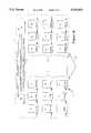
- FIG. 2wherein the physical arrangement of DRAMs 10 and driver 15 are illustrated on SIMM 5.
- the SIMM 5is noted to have two contact regions 50a and 50b on the lower edge of SIMM 5.
- Contact regions 50a and 50bconsist of narrowly spaced conductive contact pads running longitudinally across the bottom edge of SIMM 5 from pin 0 to pin 199, corresponding in number to the connector map; illustrated in FIGS. 4a and 4b and the pinout summary in Table 1 illustrated below
- FIG. 2aa detail of the bottom edge of SIMMS is shown in FIG. 2a, a magnified view of the contact region of contact regions 50a and 50b are shown in perspective view.
- contact regions 50a and 50bconsist of a large number of closely spaced contact pads 35 on the obverse side of SIMMS and a mirror image yet electrically distinct set of contact pads 36 on the reverse side of SIMMS.
- the SIMM 5 of the present inventiondoubles the pinout capacity of a SIMM by "breaking" the connection between the obverse and reverse sides of SIMM S, thereby effectively doubling the edge area which may be dedicated to electrical functions.
- the spacing of contacts 35 and 36 on SIMMSare placed on 0.050" centers, the contact pads 35 and 36 themselves being 0.040" in lateral dimension thereby yielding a space of 0.010" between contact pads.
- the precise spacing and dimensionsis not specific to the present invention, and it will be obvious to those skilled in the art that numerous spacing and pad placement schemes are possible using the "dual read out" arrangement as illustrated in FIG. 2a in contact regions 50a and 50b.
- the reduced spacing and dual readout arrangement of contact regions 50a and 50bprovide a vastly improved pinout density available for SIMM modules, over four times that suggested by Clayton.
- the full data path width of 144 bits in addition to control signals and power and ground connectionsis accommodated by connector 30 and connector regions 50a and 50b of SIMMS.
- SIMM 5constructed according to the teachings of the present invention is that memory expansion may be accommodated in full data path width increments.
- memorymay be expanded one SIMM at a time, and does not require multiple modules to be inserted to gain a single increment in memory expansion. The above result is principally derived from the accommodation of a full data path signal path on SIMM S, thus facilitating easy installation of additional memory.
- connector 30further provides for power and ground to be connected to all DRAMs 10 and driver 15. Notably, all power and ground leads are symmetrically arranged within Connector 30, as is more clearly seen in
- VCCPower
- GNDground
- SIMM 5may be used with memory arrangements other than the integrated data and video memory incorporated by reference from the above-referenced copending application.
- SIMM 5is optimally designed for use in the integrated video memory, and the user would derive optimal benefit from use in such a system.
Landscapes
- Engineering & Computer Science (AREA)
- Microelectronics & Electronic Packaging (AREA)
- Dram (AREA)
- Coupling Device And Connection With Printed Circuit (AREA)
- Credit Cards Or The Like (AREA)
- Techniques For Improving Reliability Of Storages (AREA)
- Memory System (AREA)
Abstract
Description
This application is a continuation application of Ser. No. 08/345,477, filed Nov. 28, 1994, now U.S. Pat. No. 5,465,229, which is a continuation of Ser. No. 08/279,824, filed Jul. 25, 1994, now U.S. Pat. No. 5,383,148, abandoned, which is a continuation of Ser. No. 08/115,438, filed Sep. 1, 1993, now U.S. Pat. No. 5,270,964, which is a continuation of Ser. No. 07/886,413, filed May 19, 1992.
This application is related to U.S. Pat. No. 5,260,892, entitled `High Speed Electrical Signal Interconnect Structure`, issued Nov. 9, 1993, and U.S. Pat. No. 5,266,218, entitled `Bus Architecture for Integrated Data and video Memory`, issued Nov. 23, 1993.
1. Field of the Invention
The present invention relates to the field of computer systems and memory hardware. More particularly, the present invention relates to modular circuit boards which may be combined to form a memory structure within a computer system.
3. Art Background
Single In-Line Memory Modules ("SIMMs") are compact circuit boards designed to accommodate surface mount memory chips. SIMMs were developed to provide compact and easy to manage modular memory components for user installation in computer systems designed to accept such SIMMs. SIMMs generally are easily inserted into a connector within the computer system, the SIMM thereby deriving all necessary power, ground, and logic signals therefrom.
A SIMM typically comprises a multiplicity of random access memory ("RAM") chips mounted to a printed circuit board. Depending on the user's needs, the RAM memory chips may be dynamic RAM (DRAM), non volatile static RAM (SRAM) or video RAM (VRAM). Because DRAM memories are larger and cheaper than memory cells for SRAMs, DRAMs are widely used as the principal building block for main memories in computer systems. SRAM and VRAM SIMMs have more limited application for special purposes such as extremely fast cache memories and video frame buffers, respectively. Because DRAMs form the largest portion of a computer system memory, it is therefore desirable that memory modules flexibly accommodate the computation needs of a user as the users' requirements change over time. Moreover, it is desirable that the SIMM modules may be added to the computer system with a minimum user difficulty, specifically in terms of configuration of a SIMM within a particular memory structure. In the past, SIMMs have generally been designed to provide memory increments of one or more megabytes (MB), but where the memory addition comprises only a portion of the full data path used in the computer system. A leading example of the prior art organization and structure is that disclosed in U.S. Pat/ No. 4,656,605, issued Apr. 7, 1987 to Clayton. Clayton discloses a compact modular memory circuit board to which are mounted nine memory chips which are arranged to provide memory increments in eight bit (one byte) data widths, plus parity bits. Thus, because most computer systems use data paths of 32, 64 or more bits, the SIMM constructed according to Clayton cannot provide a memory increment for the entire data path. Instead the user must obtain and install multiple SIMMs, in combination with performing any additional configuration requirements necessary to make the separate SIMMs modules function as a single memory unit, such as setting base addresses for the SIMM modules installed.
As a result, a user seeking to increase his usable main memory by adding SIMMs constructed according to the prior art, typically must insert multiple SIMMs to achieve a memory expansion for the entire data path of his computer. The foregoing is a consequence of typical prior art SIMM architecture, wherein the SIMM is arranged around DRAM parts which comprise one byte wide memory increments. Thus in a data path having a width of 32 bits, there being eight bits per byte, a 1 megabyte expansion of main memory using SIMMs constructed according to the prior art would require four SIMM modules each of one megabyte capacity in order to obtain a full data path expansion of one megabyte.
As will be described in more detail in the following detailed description, the present invention provides, among other attributes, facility for providing memory expansion in full data path widths, thereby relieving the user of configuring and installing multiple SIMMs modules to obtain any desired memory increment.
A full width single in-line memory module (SIMM) for dynamic random access memory (DRAM) memory expansions is disclosed. A printed circuit board having a multiplicity of DRAM memory elements mounted thereto is arranged in a data path having a width of 144 bits. The SIMM of the present invention further includes on-board drivers to buffer and drive signals in close proximity to the memory elements. In addition, electrically conductive traces are routed on the circuit board in such a manner to reduce loading and trace capacitance to minimize signal skew to the distributed memory elements. The SIMM further includes a high pin density dual read-out connector structure receiving electrical traces from both sides of the circuit board for enhanced functionality. The SIMM is installed in complementary sockets one SIMM at a time to provide memory expansion in full width increments. Finally, symmetrical power and ground routings to the connector structure insure that the SIMM cannot be inserted incorrectly, wherein physically reversing the SIMM in the connector slot will not reverse power the SIMM.
The objects, features and advantages of the present invention will be apparent from the following detailed description given below and from the accompanying drawings of the preferred embodiment of the invention in which:
FIG. 1a illustrates the electrical schematic of a first side of the single in-line memory module (SIMM) according to the teachings of the present invention.
FIG. 1b illustrates the electrical schematic for a left-to-right mirror image layout of memory elements on a second side of the SIMM.
FIG. 2a illustrates the physical layout of the memory elements and drivers placed on the SIMM.
FIG. 2b is a magnified view of the dual read-out connector structure on the SIMM.
FIG. 3 illustrates the stacked conductive layers separated by insulating dielectric necessary to build up the interconnections for the electrical schematic shown in FIGS. 1a and 1b.
FIGS. 4a and 4b are a connector diagram illustrating the data, address and control signals routed to the SIMM, routed to the SIMM.
A bus architecture for integrated data and video memory is disclosed. In the following description, for purposes of explanation, specific numbers, times, signals etc., are set forth in order to provide a thorough understanding of the present invention. However, it will be apparent to one skilled in the art that the present invention may be practiced without these specific details. In other instances, well known circuits and devices are shown in block diagram form in order not to obscure the present invention unnecessarily.
The preferred embodiment of the SIMM described herein is designed and intended to be used with the integrated data and video memory bus disclosed in copending U.S. patent application Ser. No. 07/886,671, filed May 19, 1992, entitled "A Bus Architecture For Integrated Data and Video Memory".
It will be apparent, however, to those skilled in the art that the specifications disclosed herein can or may be changed without departing from the scope of the present invention. Although the preferred embodiment of the present invention is disclosed in terms of the data path width matching that of the integrated data and video memory bus disclosed in the above-referenced U.S. patent application, it will be appreciated that changing the design of the bus is within the scope of the present invention, wherein the SIMM may be matched to the data path width of the integrated memory bus.
Reference is now made to FIG. 1a wherein an electrical block diagram of memory elements mounted to a first, obverse side of the SIMM is shown. In FIG. 1a, a multiplicity of dynamic RAM (DRAMs) 10 are grouped into twoclusters DRAMs 10 in each cluster. Adriver 15 receives control signals, and address signals from an external bus arrangement (not shown) through a dualsided connector 30. A multiplicity ofcontrol lines 20 route RAS-(row access strobe), CAS- (column access strobe), WE- (write enable), and OE- (output enable), control signals fromdriver 15 to all theDRAMs 10 mounted toSIMM 5. Moreover,driver 15 buffers and subsequently distributes address signals 21 to allDRAMs 10 mounted toSIMM 5. For purposes of clarity in the present figure, the specific routing of data, address and control lines to all theDRAMs 10 is omitted. However, as can be seen from FIG. 1a, allDRAMs 10 have four data lines,DRAMs 10 being any of several commercially available DRAMs arranged in a "by-four" configuration. As will be seen below in connection with FIG. 1b,DRAMs 10 each ofDRAM dusters mirror image DRAMs 10 mounted to the opposite side ofSIMM 5 and placed in electrical communication by electrical traces passing through a multiplicity of vias (not shown).
The specific routing of the electrical traces onSIMM 5 are dependent upon the specific architecture of the memory chips chosen for a specific implementation ofSIMM 5. However, allSIMMs 5 constructed according to the teachings of the present invention have a full width data path extending fromconnector 30 to all devices operating onSIMM 5, including allDRAMs 10,driver 15, and any other logic elements necessary to implement the desired function ofSIMM 5. As presently preferred,SIMM 5 embodies a 144 bit data path, comprising 128 data lines (DATA[127:0]), 16 error correction lines (CBW[15:0]) which implement a known error correction code, one EAS-, two CAS- signals, one WE signal and one reset line. The routing for all control signals 20, address signals 21 and data signals 25 minimize conductive trace capacitance and loading in accordance with U.S. Pat. No. 5,260,892, entitled `High Speed Electrical Signal Interconnect Structure ', assigned to the assignee of the present invention, and which is incorporated herein by reference. The trace routing control for all control signals 20 are taken fromdriver 15 to thecentral DRAM 10 for eachDRAM cluster central DRAM 10 are coupled to controlsignals 20 via short sub traces (not shown), thereby minimizing total capacitance, and increasing signal rise times.
With brief reference to FIG. 3, the stack up used to route all control, addresses, data, and power and ground signals is illustrated.
With brief reference to FIG. 1b, a second, reverse side ofSIMM 5 is shown. In FIG. 1b, twoadditional DRAM clusters DRAM clusters DRAM 10 inDRAM clusters driver 15 on the obverse side through conductive vias to the mirror image reverse side of SIMM 5., thereby doubling the available surface area to whichDRAMs 10 may be mounted. Moreover,SIMM 5 as presently preferred utilized thin small outline package (TSOP)DRAMs 10 to reduce overall thickness ofSIMMs 5. When thus constructed, the double sidedSIMM 5 of the present invention is no thicker than prior art single sided SIMMs (e.g., as taught by Clayton).
Briefly referring to FIG. 4, the highnumber density connector 30 used to connectSIMM 5 to the memory module socket (not shown) is illustrated. In FIG. 4,connector 30 is seen to have 200 pin terminations, therefore permitting a large number of signals to be routed to and fromSIMM 5. In the preferred embodiment ofSIMM 5, it is intended thatSIMM 5 specifically incorporate the data path architecture consistent with an integrated data and video memory bus such as that described in above referenced copending U.S. patent applications assigned to Sun Microsystems, Inc., Mountain View, Calif., which is hereby incorporated herein by reference. In particular, the data path architecture implemented onSIMM 5 includes 128 data lines, 16 error correction code lines (referred to CBW [15:0] in FIGS. 1-6), in addition to a multiplicity of control signals necessary to accomplish DRAM memory accesses. Such control signals, collectively referred to controllines 20 in FIGS. 1a and 1b, include one RAS- signal, two CAS- signals, one WE- signal, and one reset line per SIMM. Thus, not including the control signals 20 which are used for controlling operation ofDRAMs 10, the data path used for transmission of data to and fromDKAMs 10 is seen to be 144 bites wide. Disregarding the error correction code signals, referred to in FIGS. 1-6 as CBW [15:0], the actual data path width ofSIMM 5 for writing and reading data to and from memory is 128 bits wide, or sixteen bites, identical to that of the integrated data and video memory bus. Accordingly, SIMM5 of the present invention may be installed into the memory bus in full width increments.
A total memory capacity available on aSIMM 5 may be computed as follows. Depending on the capacity of eachRAM 10 mounted toSIMM 5 the total memory capacity of eachSIMM module 5 can vary from four megabytes (MB) to a maximum of sixty-four MB, distributed over a total of thirty-sixDRAMs 10. Using commercially available 256K×4 1Mbit DRAMs 10, four megabytes of memory may be provided onSIMM 5. Alternatively, when 16 megabit parts become available, because the addressable address space ofSIMM 5 is very large, greater than two gigabits,SIMM 5 can easily accommodate the higher 16 megabit parts and make available a total capacity of 64 megabytes on aSIMM 5 having 36 DRAMs mounted to it.
Operation ofSIMM 5 is controlled bycontrol signals 20 as will be briefly discussed below. For a complete discussion on the actual operation ofSIMM 5 in connection with the integrated data and video bus, the reader is referred to the above copending U.S. patent application, entitled "A Bus Architecture".
Reference is now made to FIG. 2, wherein the physical arrangement ofDRAMs 10 anddriver 15 are illustrated onSIMM 5. In addition to theDRAM clusters SIMM 5, theSIMM 5 is noted to have two contact regions 50a and 50b on the lower edge ofSIMM 5. Contact regions 50a and 50b consist of narrowly spaced conductive contact pads running longitudinally across the bottom edge ofSIMM 5 frompin 0 to pin 199, corresponding in number to the connector map; illustrated in FIGS. 4a and 4b and the pinout summary in Table 1 illustrated below
TABLE 1 ______________________________________ SIMM Pin Descriptions Pin Descriptions ______________________________________ D<0-127 Data Bits A<0-11> Address Bits CBW<0-7> Check Bit Write Enables/data bus to on board devices used in Video SIMM CBW<8-5> Check Bit Write Enables CAS<0-1>* Column Address Strobes RAS<0-1>* Row Address Strobes BUSY* Video Frame Buffer Busy Signal - indicates that frame buffer is busy doing refresh or reload operations SIRQ* UART Interrupt VIRQ* Video Interrupt WE* Write Enable MRST* Reset Signal MCLK MBus Clock - Sent to the VBC IOSEL* Differentiates between memory address space and I/O address space ROE* Currently used by VSIMM to generate DTOE signals. OE* on the DSIMMs is tied to Ground. ______________________________________
a detail of the bottom edge of SIMMS is shown in FIG. 2a, a magnified view of the contact region of contact regions 50a and 50b are shown in perspective view. In FIG. 2a, it is seen that contact regions 50a and 50b consist of a large number of closely spacedcontact pads 35 on the obverse side of SIMMS and a mirror image yet electrically distinct set ofcontact pads 36 on the reverse side of SIMMS. In contrast to SIMMs constructed according to the prior art, theSIMM 5 of the present invention doubles the pinout capacity of a SIMM by "breaking" the connection between the obverse and reverse sides of SIMM S, thereby effectively doubling the edge area which may be dedicated to electrical functions. For purposes of clarity, in contrast to prior art SIMM modules having contact pins placed on 0.1" centers, the spacing ofcontacts contact pads SIMM 5, the full data path width of 144 bits in addition to control signals and power and ground connections is accommodated byconnector 30 and connector regions 50a and 50b of SIMMS.
As previously noted in connection with the memory capacities according to the type ofDRAM 10 installed onSIMM 5, it should be appreciated that the principal benefit ofSIMM 5 constructed according to the teachings of the present invention is that memory expansion may be accommodated in full data path width increments. In contrast to memory expansion using SIMMs of the prior art, use ofSIMM 5 in expanding memory, especially memory in association with integrated data and video memory of the above referenced copending application, memory may be expanded one SIMM at a time, and does not require multiple modules to be inserted to gain a single increment in memory expansion. The above result is principally derived from the accommodation of a full data path signal path on SIMM S, thus facilitating easy installation of additional memory.
Finally,connector 30 further provides for power and ground to be connected to allDRAMs 10 anddriver 15. Notably, all power and ground leads are symmetrically arranged withinConnector 30, as is more clearly seen in
TABLE 2 __________________________________________________________________________base +1 +2 +3 +4 +5 +6 +7 +8 __________________________________________________________________________0 GND GND D0 D7 D1D6 D2 D5 8 D3 D4 D32 D39 D33D38 D34 D37 16 VCC VCC D35 D36 D8D15 D9 D14 24 D10 D13 D11 D12 D40D47 D41 D46 32 GND GND D42 D45 D43D44 D16 D23 40 D17 D22 D18 D21 D19D20 D48 D55 48 VCC VCC D49 D54 D50D53 D51 D52 56 D24 D31 D25 D30 D26D29 D27 D28 64 GND GND D56 D63 D57D62 D58 D61 72 D59 D60 CBWO CBW7 CBW1CBW6 CBW2 DBW5 80 VCC VCC CBW3 CBW4 CAS0CAS1 RAS0 RAS1 88 ROE BUSY VIRQ SIRQ A0A1 A2 A3 96 A4 A5 GND GND GNDGND A6 A7 104 A8 A9 A19 A11 MRSTWE IOSEL MCLK 112 GND GND GND GND CBW8CBW15 VCC VCC 120 CBW9 CBW14 CBW10 CBW13 CBW11 CBW12 D64 D71 128 D65 D70 D66 D69 D67 D68 GND GND 136 D96 D103 D97 D102 D98D101 D99 D100 144 D72 D79 D73 D78 D74 D77 VCC VCC 152 D75 D76 D104 D111 D105 D110 D106 D109 160 D107 D108 D80 D87 D81 D86 GND GND 168 D82 D85 D83 D84 D112 D119 D113 D118 176 D114 D117 D115 D116 D88 D95 VCC VCC 184 D89 D94 D90 D93 D91 D92 D120 D127 192 D121 D126 D122 D125 D123 D124 GND GND __________________________________________________________________________
Power (VCC) and ground (GND) leads are seen to alternate every sixteen pins. If a SIMMS were inadvertently inserted in a reversed position into a memory module socket, the symmetrical power ground leads prevent theSIMM 5 from being reverse-powered, and likely destroyed.
The foregoing has described a physical architecture for a single in-line memory module compatible with an integrated data and video memory. It is contemplated that changes and modifications may be made by one or ordinary skill in the art, to the device components and arrangements of the elements of the present invention without departing from the spirit and scope of the invention. In particular, it is anticipated thatSIMM 5 may be used with memory arrangements other than the integrated data and video memory incorporated by reference from the above-referenced copending application. However,SIMM 5 is optimally designed for use in the integrated video memory, and the user would derive optimal benefit from use in such a system.
While the invention has been described in conjunction with the preferred embodiment, it is evident that numerous alternative modifications, variations and uses will be apparent to those skilled in the art in light of the foregoing description.
Claims (25)
1. A single in-line memory module for memory expansion in a computer system having a memory bus with n data lines, said single in-line memory module comprising the elements of:
a printed circuit board, said printed circuit board having a first side and a second side, said printed circuit board having an electrical connectors, said electrical connector comprising a first set of electrical contacts on said first side of said printed circuit board and a second set of electrical contacts on said second side of said printed circuit board, wherein said electrical connector includes a full width data path;
a first set of memory elements arranged on said printed circuit board; and
a second set of memory elements arranged on said printed circuit board, said first and second set of memory elements having a total of at least n data lines;
a set of control signals in said electrical connector electrically coupled to said first set of memory elements and said second set of memory elements.
2. A single in-line memory module as claimed in claim 1 one of said single in-line memory modules can increase a main memory in said computer system.
3. A single in-line memory module as claimed in claim 1 wherein said single in-line memory module provides data in a first data path at least as wide a second data path used by a central processing unit in said computer system.
4. The single in-line memory module for memory expansion of claim 1 wherein said first set of electrical contacts and said second set of electrical contacts are electrically distinct.
5. A single in-line memory module as claimed in claim 1 wherein said electrical connector has symmetrical power and ground contacts for preventing damage to said single in-line memory module if said single in-line memory module is inserted into said computer system backwards.
6. A single in-line memory module as claimed in claim 1 wherein said single in-line memory module further comprises:
a driver circuit mounted substantially centered on said first side of said printed circuit board, said driver circuit coupled to a set control signals in said electrical connector, said driver circuit transmitting said controls signals to said first set of memory elements and said second set of memory elements.
7. A single in-line memory module as claimed in claim 6 wherein:
said first set of memory elements is arranged on the first side of said printed circuit board and comprises a first subset arranged to the left of said driver circuit and a second subset arranged to the right of said driver circuit; and
said second set of memory elements is arranged on the second side of said printed circuit board and comprises a third subset positioned opposite said first subset and a fourth subset positioned opposite said second subset.
8. A single in-line memory module as claimed in claim 7 wherein said first, second, third, and fourth subsets of memory elements each comprise nine memory elements arranged in a three by three matrix and said driver circuit transmits said control signals directly to a center memory element in said first and second memory element subsets such that signal skew is minimized.
9. A single in-line memory module as claimed in claim 8 wherein said control signals comprise column address strobe (CAS), row address strobe (RAS), write enable (WE), and output enable (OE) signals.
10. A single in-line memory module as claimed in claim 9 wherein said driver circuit further drives address lines.
11. A single in-line memory module as claimed in claim 9 wherein said electrical connector has symmetrical power and ground contacts such that said single in-line memory module is not damaged in said single in-line memory module is inserted into said computer system backwards.
12. A single in-line memory module as claimed in claim 6 wherein said single in-line memory module provides data in a first data path at least as wide a second data path used by a central processing unit in said computer system.
13. A single in-line memory module as claimed in claim 1 wherein said single in-line memory module further comprises the elements of:
a second set of memory elements arranged on said printed circuit board, said first and second set of memory elements having a total of at least n data lines; and
a driver circuit mounted substantially centered on said first side of said printed circuit board, said driver circuit coupled to a set of control signals in said electrical connector, said driver circuit transmitting said controls signals to said first set of memory elements and said second set of memory elements.
14. The single in-line memory module as claimed in claim 1 wherein said full width data path includes a plurality of error correction lines.
15. A single in-line memory module for memory expansion in a computer system having a memory bus, said single in=line memory module comprising the elements of:
a printed circuit board, said printed circuit board having a first side and a second side, said printed circuit board having an electrical connector, said electrical connector comprising a first set of electrical contacts on said first side of said printed circuit board and a second set of electrical contacts on said second side of said printed circuit board;
a first set of memory elements arranged on said printed circuit board; and
a driver circuit mounted on said printed circuit board, said driver circuit coupled to a set of control signals in said electrical connector, said driver circuit transmitting said controls signals to said first set of memory elements;
wherein said first set of electrical contacts and said second set of electrical contacts are electrically distinct.
16. The single in-line memory module as claimed in claim 15 wherein said full width data path includes a plurality of error correction lines.-t
17. A single in-line memory module for memory expansion in a computer system having a memory bus, said single in-line memory module comprising the elements of:
a printed circuit board, said printed circuit board having a first side and a second side, said printed circuit board having an electrical connector, said electrical connector comprising a first set of electrical contacts on said first side of said printed circuit board and a second set of electrical contacts on said second side of said printed circuit board;
a first set of memory elements arranged on said first side of said printed circuit board, said first set of memory elements coupled to first set of electrical contacts;
a second set of memory elements arranged on second side of said printed circuit board, said second set of memory elements coupled to second set of electrical contacts; and
a driver circuit mounted on said printed circuit board, said driver circuit coupled to a set of control signals in said electrical connector, said driver circuit transmitting said controls signals to said first set of memory elements;
wherein said first set of electrical contacts and said second set of electrical contacts are electrically distinct.
18. A single in-line memory module for memory expansion in a computer system having a memory bus, said single in-line memory module comprising the elements of:
a printed circuit board, said printed circuit board having a first side and a second side, said printed circuit board having an electrical connector, said electrical connector having a first set of electrical contacts and a second set of electrical contacts;
a first set of memory elements arranged on said printed circuit board; and
a driver circuit mounted on said printed circuit board, said driver circuit coupled to a set of control signals in said electrical connector, said driver circuit transmitting said controls signals to said first set of memory elements
wherein said first set of electrical contacts and said second set of electrical contacts are electrically distinct.
19. A single in-line memory module for memory expansion in a computer system having a memory bus with n data lines, said single in-line memory module comprising the elements of:
a printed circuit board, said printed circuit board having a first side and a second side, said printed circuit board having an electrical connector, said electrical connector comprising a first set of electrical contacts on said first side of said printed circuit board and a second set of electrical contacts on said second side of said printed circuit board;
a first set of memory elements arranged on said printed circuit board, said set of memory elements having a total of at least n data lines; and
a driver circuit mounted on said printed circuit board, said driver circuit coupled to a set of control signals in said electrical connector, said driver circuit transmitting said controls signals to said first set of memory elements;
wherein said first set of electrical contacts and said second set of electrical contacts are electrically distinct.
20. A single in-line memory module for memory expansion in a computer system having a memory bus with n data lines, said single in-line memory module comprising the elements of:
a printed circuit board, said printed circuit board having a first side and a second side, said printed circuit board having an electrical connector, said electrical connector comprising a first set of electrical contacts on said first side of printed circuit board and a second set of electrical contacts on said second side of said printed circuit board;
a first set of memory elements arranged on said first side of said printed circuit board, said first set of memory elements coupled to firs set of electrical contacts;
a second set of memory elements arranged on second side of said printed circuit board, said second set of memory elements coupled to second set of electrical contacts, said first and second set of memory elements having a total of at least n data lines; and
a driver circuit mounted on said printed circuit board, said driver circuit coupled to a set of control signals in said electrical connector, said driver circuit transmitting said controls signals to said first set of memory elements;
wherein said first set of electrical contacts and said second set of electrical contacts are electrically distinct.
21. A single in-line memory module for memory expansion in a computer system having a memory bus with n data lines, said single in-line memory module comprising the elements of:
a printed circuitry board, said printed circuit board having a first side and a second side, said printed circuit board having an electrical connector, said electrical connector having a first set of electrical contacts and a second set of electrical contacts;
a first set of memory elements arranged on said printed circuit board, said set of memory elements having a total of at least n data lines; and
a driver circuit mounted on said printed circuit board, said driver circuit coupled to a set of control signals in said electrical connector, said driver circuit transmitting said controls signals to said first set of memory elements
where in said first set of electrical contacts and said second set of electrical contacts are electrically distinct.
22. A single in-line memory module for memory expansion in a computer system having a memory bus with n data lines, said single in-line memory module comprising the elements of:
a printed circuit board, said printed circuit board having a first side and a second side, said printed circuit board having an electrical connector, said electrical connector comprising a first set of electrical contacts on said first side of said printed circuit board and a second set of electrical contacts on said second side of said printed circuit board;
a first set of memory elements arranged on said printed circuit board, said set of memory elements having a total of at least n data lines; and
a driver circuit mounted on said printed circuit board, said driver circuit coupled to a set of control signals in said electrical connector, said driver circuit transmitting said controls signals to said first set of memory elements
where in said electrical connector includes a full width data path such that one of said single in-line memory modules can increase a main memory in said computer system.
23. A memory structure for a computer system comprising:
an integrated video and data memory bus with n data lines; and
at least one single in-line memory module having:
a printed circuit board, said printed circuit board having a first side and a second side, said printed circuit board having an electrical connector, said electrical connector comprising a first set of electrical contacts on said first side of said printed circuit board and a second set of electrical contacts on said second side of said printed circuit board;
a first set of memory elements arranged on said printed circuit board; and
a second set of memory elements arranged on said printed circuit board, said first and second set of memory elements configured for integrated data and video storage and having a total of at least n data lines comprising a full width data path; a set of control signals in said electrical connector electrically coupled to said first set of memory elements and said second set of memory elements.
24. A memory structure for a computer system comprising:
an integrated video and data memory bus; and
at least one single in-line memory module having:
a printed circuit board, said printed circuit board having a first side and a second side, said printed circuit board having an electrical connector, said electrical connector comprising a first set of electrical contacts on said first side of said printed circuit board and a second set of electrical contacts on said second side of said printed circuit board;
a first set of memory elements arranged on said printed circuit board and configured for integrated data and video storage; and
a driver circuit mounted on said printed circuit board, said driver circuit coupled to a set of control signals in said electrical connector, said driver circuit transmitting said controls signals to said first set of memory elements;
wherein said first set of electrical contacts and said second set of electrical contacts are electrically distinct.
25. A single in-line memory module for memory expansion in a computer system having a memory bus, said single in-line memory module comprising the elements of:
a printed circuit board, said printed circuit board having a first side and a second side, said printed circuit board-having an electrical connector, said electrical connector comprising a first set of electrical contacts on said first side of said printed circuit board and a second set of electrical contacts on said second side of said printed circuit board; and
a first set of memory elements arranged on said printed circuit board;
wherein said first set of electrical contacts and said second set of electrical contacts are electrically distinct.
Priority Applications (2)
| Application Number | Priority Date | Filing Date | Title |
|---|---|---|---|
| US08/473,073US5532954A (en) | 1992-05-19 | 1995-06-07 | Single in-line memory module |
| US08/878,705US5973951A (en) | 1992-05-19 | 1997-06-19 | Single in-line memory module |
Applications Claiming Priority (5)
| Application Number | Priority Date | Filing Date | Title |
|---|---|---|---|
| US07/886,413US5270964A (en) | 1992-05-19 | 1992-05-19 | Single in-line memory module |
| US11543893A | 1993-09-01 | 1993-09-01 | |
| US08/279,824US5383148A (en) | 1992-05-19 | 1994-07-25 | Single in-line memory module |
| US08/345,477US5465229A (en) | 1992-05-19 | 1994-11-28 | Single in-line memory module |
| US08/473,073US5532954A (en) | 1992-05-19 | 1995-06-07 | Single in-line memory module |
Related Parent Applications (1)
| Application Number | Title | Priority Date | Filing Date |
|---|---|---|---|
| US08/345,477ContinuationUS5465229A (en) | 1992-05-19 | 1994-11-28 | Single in-line memory module |
Related Child Applications (1)
| Application Number | Title | Priority Date | Filing Date |
|---|---|---|---|
| US64309496AContinuation | 1992-05-19 | 1996-05-02 |
Publications (1)
| Publication Number | Publication Date |
|---|---|
| US5532954Atrue US5532954A (en) | 1996-07-02 |
Family
ID=25389005
Family Applications (5)
| Application Number | Title | Priority Date | Filing Date |
|---|---|---|---|
| US07/886,413Expired - Fee RelatedUS5270964A (en) | 1992-05-19 | 1992-05-19 | Single in-line memory module |
| US08/279,824Expired - LifetimeUS5383148A (en) | 1992-05-19 | 1994-07-25 | Single in-line memory module |
| US08/345,477Expired - LifetimeUS5465229A (en) | 1992-05-19 | 1994-11-28 | Single in-line memory module |
| US08/473,073Expired - LifetimeUS5532954A (en) | 1992-05-19 | 1995-06-07 | Single in-line memory module |
| US08/878,705Expired - LifetimeUS5973951A (en) | 1992-05-19 | 1997-06-19 | Single in-line memory module |
Family Applications Before (3)
| Application Number | Title | Priority Date | Filing Date |
|---|---|---|---|
| US07/886,413Expired - Fee RelatedUS5270964A (en) | 1992-05-19 | 1992-05-19 | Single in-line memory module |
| US08/279,824Expired - LifetimeUS5383148A (en) | 1992-05-19 | 1994-07-25 | Single in-line memory module |
| US08/345,477Expired - LifetimeUS5465229A (en) | 1992-05-19 | 1994-11-28 | Single in-line memory module |
Family Applications After (1)
| Application Number | Title | Priority Date | Filing Date |
|---|---|---|---|
| US08/878,705Expired - LifetimeUS5973951A (en) | 1992-05-19 | 1997-06-19 | Single in-line memory module |
Country Status (6)
| Country | Link |
|---|---|
| US (5) | US5270964A (en) |
| EP (4) | EP0926681A3 (en) |
| JP (1) | JPH06348588A (en) |
| KR (1) | KR100235222B1 (en) |
| DE (1) | DE69326189T2 (en) |
| SG (1) | SG43928A1 (en) |
Cited By (34)
| Publication number | Priority date | Publication date | Assignee | Title |
|---|---|---|---|---|
| WO1997018602A1 (en)* | 1995-11-13 | 1997-05-22 | Intel Corporation | A dual-in-line universal serial bus connector |
| US5831890A (en)* | 1996-12-16 | 1998-11-03 | Sun Microsystems, Inc. | Single in-line memory module having on-board regulation circuits |
| US5870325A (en)* | 1998-04-14 | 1999-02-09 | Silicon Graphics, Inc. | Memory system with multiple addressing and control busses |
| US5877975A (en)* | 1996-08-13 | 1999-03-02 | Nexcom Technology, Inc. | Insertable/removable digital memory apparatus and methods of operation thereof |
| US5953243A (en)* | 1998-09-30 | 1999-09-14 | International Business Machines Corporation | Memory module identification |
| US5973951A (en)* | 1992-05-19 | 1999-10-26 | Sun Microsystems, Inc. | Single in-line memory module |
| US6026007A (en)* | 1996-08-13 | 2000-02-15 | Integrated Silicon Solution, Inc. | Insertable and removable high capacity digital memory apparatus and methods of operation thereof |
| WO2000026916A1 (en)* | 1998-11-04 | 2000-05-11 | Micron Electronics, Inc. | Device and method in an integrated circuit (ic) module for buffering clocks and other input signals |
| US6067594A (en)* | 1997-09-26 | 2000-05-23 | Rambus, Inc. | High frequency bus system |
| US6108228A (en)* | 1997-12-02 | 2000-08-22 | Micron Technology, Inc. | Quad in-line memory module |
| US6142830A (en)* | 1998-03-06 | 2000-11-07 | Siemens Aktiengesellschaft | Signaling improvement using extended transmission lines on high speed DIMMS |
| US6288898B1 (en) | 1999-12-20 | 2001-09-11 | Dell Usa, L.P. | Apparatus for mounting and cooling a system components in a computer |
| US6324071B2 (en) | 1999-01-14 | 2001-11-27 | Micron Technology, Inc. | Stacked printed circuit board memory module |
| US6327690B1 (en) | 1999-02-04 | 2001-12-04 | Intel Corporation | Integrated reed-solomon error correction code encoder and syndrome generator |
| US6338144B2 (en) | 1999-02-19 | 2002-01-08 | Sun Microsystems, Inc. | Computer system providing low skew clock signals to a synchronous memory unit |
| WO2002025454A3 (en)* | 2000-09-14 | 2002-08-22 | Intel Corp | Memory module having buffer for isolating stacked memory devices |
| US20030169614A1 (en)* | 2002-03-07 | 2003-09-11 | Bhakta Jayesh R. | Arrangement of integrated ciruits in a memory module |
| US6683372B1 (en) | 1999-11-18 | 2004-01-27 | Sun Microsystems, Inc. | Memory expansion module with stacked memory packages and a serial storage unit |
| US6721185B2 (en) | 2001-05-01 | 2004-04-13 | Sun Microsystems, Inc. | Memory module having balanced data I/O contacts pads |
| US6747887B2 (en) | 2000-09-18 | 2004-06-08 | Intel Corporation | Memory module having buffer for isolating stacked memory devices |
| US20050018495A1 (en)* | 2004-01-29 | 2005-01-27 | Netlist, Inc. | Arrangement of integrated circuits in a memory module |
| US20050044302A1 (en)* | 2003-08-06 | 2005-02-24 | Pauley Robert S. | Non-standard dual in-line memory modules with more than two ranks of memory per module and multiple serial-presence-detect devices to simulate multiple modules |
| US6927992B1 (en) | 2003-05-12 | 2005-08-09 | Pericom Semiconductor Corp. | Trace-impedance matching at junctions of multi-load signal traces to eliminate termination |
| KR100585158B1 (en) | 2004-09-13 | 2006-05-30 | 삼성전자주식회사 | ECC memory module |
| US20070091704A1 (en)* | 2005-10-26 | 2007-04-26 | Siva Raghuram | Memory module with an electronic printed circuit board and a plurality of semiconductor chips of the same type |
| US8516188B1 (en) | 2004-03-05 | 2013-08-20 | Netlist, Inc. | Circuit for memory module |
| US8588017B2 (en) | 2010-10-20 | 2013-11-19 | Samsung Electronics Co., Ltd. | Memory circuits, systems, and modules for performing DRAM refresh operations and methods of operating the same |
| US8756364B1 (en) | 2004-03-05 | 2014-06-17 | Netlist, Inc. | Multirank DDR memory modual with load reduction |
| US8782350B2 (en) | 2008-04-14 | 2014-07-15 | Netlist, Inc. | Circuit providing load isolation and noise reduction |
| US9128632B2 (en) | 2009-07-16 | 2015-09-08 | Netlist, Inc. | Memory module with distributed data buffers and method of operation |
| US9606907B2 (en) | 2009-07-16 | 2017-03-28 | Netlist, Inc. | Memory module with distributed data buffers and method of operation |
| US10290328B2 (en) | 2010-11-03 | 2019-05-14 | Netlist, Inc. | Memory module with packages of stacked memory chips |
| US10324841B2 (en) | 2013-07-27 | 2019-06-18 | Netlist, Inc. | Memory module with local synchronization |
| US10755757B2 (en) | 2004-01-05 | 2020-08-25 | Smart Modular Technologies, Inc. | Multi-rank memory module that emulates a memory module having a different number of ranks |
Families Citing this family (134)
| Publication number | Priority date | Publication date | Assignee | Title |
|---|---|---|---|---|
| US5446860A (en)* | 1993-01-11 | 1995-08-29 | Hewlett-Packard Company | Apparatus for determining a computer memory configuration of memory modules using presence detect bits shifted serially into a configuration register |
| US5375084A (en)* | 1993-11-08 | 1994-12-20 | International Business Machines Corporation | Selectable interface between memory controller and memory simms |
| JP3077866B2 (en)* | 1993-11-18 | 2000-08-21 | 日本電気株式会社 | Memory module |
| US5502621A (en)* | 1994-03-31 | 1996-03-26 | Hewlett-Packard Company | Mirrored pin assignment for two sided multi-chip layout |
| GB9410208D0 (en)* | 1994-05-21 | 1994-07-06 | Simpson Gareth D | Memory module |
| DE4423567C2 (en)* | 1994-07-05 | 1998-09-03 | Siemens Ag | Module card |
| US5513135A (en)* | 1994-12-02 | 1996-04-30 | International Business Machines Corporation | Synchronous memory packaged in single/dual in-line memory module and method of fabrication |
| US5577236A (en)* | 1994-12-30 | 1996-11-19 | International Business Machines Corporation | Memory controller for reading data from synchronous RAM |
| KR0144035B1 (en)* | 1995-03-07 | 1998-08-17 | 김주용 | D-ram module connecting method |
| US5686730A (en)* | 1995-05-15 | 1997-11-11 | Silicon Graphics, Inc. | Dimm pair with data memory and state memory |
| IN188196B (en)* | 1995-05-15 | 2002-08-31 | Silicon Graphics Inc | |
| US5745914A (en)* | 1996-02-09 | 1998-04-28 | International Business Machines Corporation | Technique for converting system signals from one address configuration to a different address configuration |
| US5661677A (en) | 1996-05-15 | 1997-08-26 | Micron Electronics, Inc. | Circuit and method for on-board programming of PRD Serial EEPROMS |
| US5802395A (en)* | 1996-07-08 | 1998-09-01 | International Business Machines Corporation | High density memory modules with improved data bus performance |
| EP0880142B1 (en)* | 1997-05-20 | 2011-04-27 | Bull S.A. | Dynamic random access memory (DRAM) having variable configuration for data processing system and corresponding expansion support for the interleaved-block configuration thereof |
| US6286062B1 (en)* | 1997-07-01 | 2001-09-04 | Micron Technology, Inc. | Pipelined packet-oriented memory system having a unidirectional command and address bus and a bidirectional data bus |
| US6349051B1 (en) | 1998-01-29 | 2002-02-19 | Micron Technology, Inc. | High speed data bus |
| US6721860B2 (en) | 1998-01-29 | 2004-04-13 | Micron Technology, Inc. | Method for bus capacitance reduction |
| US6108730A (en) | 1998-02-27 | 2000-08-22 | International Business Machines Corporation | Memory card adapter insertable into a motherboard memory card socket comprising a memory card receiving socket having the same configuration as the motherboard memory card socket |
| KR100355223B1 (en)* | 1999-01-07 | 2002-10-09 | 삼성전자 주식회사 | Multi in-line memory module and the electronic component socket therefor |
| US6115278A (en) | 1999-02-09 | 2000-09-05 | Silicon Graphics, Inc. | Memory system with switching for data isolation |
| US6315614B1 (en)* | 1999-04-16 | 2001-11-13 | Sun Microsystems, Inc. | Memory module with offset notches for improved insertion and stability and memory module connector |
| US6414868B1 (en) | 1999-06-07 | 2002-07-02 | Sun Microsystems, Inc. | Memory expansion module including multiple memory banks and a bank control circuit |
| US6574746B1 (en) | 1999-07-02 | 2003-06-03 | Sun Microsystems, Inc. | System and method for improving multi-bit error protection in computer memory systems |
| US6408356B1 (en) | 1999-11-16 | 2002-06-18 | International Business Machines Corporation | Apparatus and method for modifying signals from a CPU to a memory card |
| US7010642B2 (en) | 2000-01-05 | 2006-03-07 | Rambus Inc. | System featuring a controller device and a memory module that includes an integrated circuit buffer device and a plurality of integrated circuit memory devices |
| TW523658B (en)* | 2000-04-29 | 2003-03-11 | Samsung Electronics Co Ltd | Memory modules having conductors at edges thereof and configured to conduct signals to and from the memory modules via the respective edges |
| US6791555B1 (en) | 2000-06-23 | 2004-09-14 | Micron Technology, Inc. | Apparatus and method for distributed memory control in a graphics processing system |
| GB2366470B (en)* | 2000-08-25 | 2005-07-20 | Hewlett Packard Co | Improvements relating to document transmission techniques iv |
| GB2366468B (en)* | 2000-08-25 | 2005-03-02 | Hewlett Packard Co | Improvements relating to document transmission techniques I |
| GB2366469B (en)* | 2000-08-25 | 2005-02-23 | Hewlett Packard Co | Improvements relating to document transmission techniques II |
| US6658530B1 (en)* | 2000-10-12 | 2003-12-02 | Sun Microsystems, Inc. | High-performance memory module |
| US6725314B1 (en) | 2001-03-30 | 2004-04-20 | Sun Microsystems, Inc. | Multi-bank memory subsystem employing an arrangement of multiple memory modules |
| US6714433B2 (en) | 2001-06-15 | 2004-03-30 | Sun Microsystems, Inc. | Memory module with equal driver loading |
| US6843421B2 (en) | 2001-08-13 | 2005-01-18 | Matrix Semiconductor, Inc. | Molded memory module and method of making the module absent a substrate support |
| US6674644B2 (en) | 2001-11-01 | 2004-01-06 | Sun Microsystems, Inc. | Module and connector having multiple contact rows |
| US20030101312A1 (en)* | 2001-11-26 | 2003-05-29 | Doan Trung T. | Machine state storage apparatus and method |
| US6731011B2 (en)* | 2002-02-19 | 2004-05-04 | Matrix Semiconductor, Inc. | Memory module having interconnected and stacked integrated circuits |
| US6771536B2 (en) | 2002-02-27 | 2004-08-03 | Sandisk Corporation | Operating techniques for reducing program and read disturbs of a non-volatile memory |
| US7076408B1 (en)* | 2002-04-03 | 2006-07-11 | Yazaki North America | Method for ensuring consistent protocol in the location of circuits and connectors having multiple circuit-receiving cavities |
| US7133972B2 (en)* | 2002-06-07 | 2006-11-07 | Micron Technology, Inc. | Memory hub with internal cache and/or memory access prediction |
| US7200024B2 (en) | 2002-08-02 | 2007-04-03 | Micron Technology, Inc. | System and method for optically interconnecting memory devices |
| US7117316B2 (en) | 2002-08-05 | 2006-10-03 | Micron Technology, Inc. | Memory hub and access method having internal row caching |
| US7254331B2 (en) | 2002-08-09 | 2007-08-07 | Micron Technology, Inc. | System and method for multiple bit optical data transmission in memory systems |
| US7149874B2 (en) | 2002-08-16 | 2006-12-12 | Micron Technology, Inc. | Memory hub bypass circuit and method |
| US6820181B2 (en) | 2002-08-29 | 2004-11-16 | Micron Technology, Inc. | Method and system for controlling memory accesses to memory modules having a memory hub architecture |
| US7836252B2 (en) | 2002-08-29 | 2010-11-16 | Micron Technology, Inc. | System and method for optimizing interconnections of memory devices in a multichip module |
| US7102907B2 (en) | 2002-09-09 | 2006-09-05 | Micron Technology, Inc. | Wavelength division multiplexed memory module, memory system and method |
| KR100505641B1 (en)* | 2002-09-10 | 2005-08-03 | 삼성전자주식회사 | Memory module and memory system having the same |
| US6996686B2 (en)* | 2002-12-23 | 2006-02-07 | Sun Microsystems, Inc. | Memory subsystem including memory modules having multiple banks |
| US6812555B2 (en)* | 2003-03-10 | 2004-11-02 | Everstone Industry Corp. | Memory card substrate with alternating contacts |
| US6982892B2 (en)* | 2003-05-08 | 2006-01-03 | Micron Technology, Inc. | Apparatus and methods for a physical layout of simultaneously sub-accessible memory modules |
| US7245145B2 (en) | 2003-06-11 | 2007-07-17 | Micron Technology, Inc. | Memory module and method having improved signal routing topology |
| US7120727B2 (en) | 2003-06-19 | 2006-10-10 | Micron Technology, Inc. | Reconfigurable memory module and method |
| US7260685B2 (en) | 2003-06-20 | 2007-08-21 | Micron Technology, Inc. | Memory hub and access method having internal prefetch buffers |
| US7107415B2 (en) | 2003-06-20 | 2006-09-12 | Micron Technology, Inc. | Posted write buffers and methods of posting write requests in memory modules |
| US7428644B2 (en) | 2003-06-20 | 2008-09-23 | Micron Technology, Inc. | System and method for selective memory module power management |
| KR100568537B1 (en) | 2003-06-24 | 2006-04-07 | 삼성전자주식회사 | Buffered memory module |
| US7389364B2 (en) | 2003-07-22 | 2008-06-17 | Micron Technology, Inc. | Apparatus and method for direct memory access in a hub-based memory system |
| CN100474709C (en)* | 2003-07-28 | 2009-04-01 | 桑迪士克防护内容解决公司 | Electrical connector |
| US7210059B2 (en) | 2003-08-19 | 2007-04-24 | Micron Technology, Inc. | System and method for on-board diagnostics of memory modules |
| US7133991B2 (en) | 2003-08-20 | 2006-11-07 | Micron Technology, Inc. | Method and system for capturing and bypassing memory transactions in a hub-based memory system |
| US7136958B2 (en) | 2003-08-28 | 2006-11-14 | Micron Technology, Inc. | Multiple processor system and method including multiple memory hub modules |
| US20050050237A1 (en)* | 2003-08-28 | 2005-03-03 | Jeddeloh Joseph M. | Memory module and method having on-board data search capabilities and processor-based system using such memory modules |
| US7310752B2 (en) | 2003-09-12 | 2007-12-18 | Micron Technology, Inc. | System and method for on-board timing margin testing of memory modules |
| US7194593B2 (en) | 2003-09-18 | 2007-03-20 | Micron Technology, Inc. | Memory hub with integrated non-volatile memory |
| US7120743B2 (en) | 2003-10-20 | 2006-10-10 | Micron Technology, Inc. | Arbitration system and method for memory responses in a hub-based memory system |
| US7234070B2 (en) | 2003-10-27 | 2007-06-19 | Micron Technology, Inc. | System and method for using a learning sequence to establish communications on a high-speed nonsynchronous interface in the absence of clock forwarding |
| US7177211B2 (en)* | 2003-11-13 | 2007-02-13 | Intel Corporation | Memory channel test fixture and method |
| US7330992B2 (en) | 2003-12-29 | 2008-02-12 | Micron Technology, Inc. | System and method for read synchronization of memory modules |
| US7188219B2 (en) | 2004-01-30 | 2007-03-06 | Micron Technology, Inc. | Buffer control system and method for a memory system having outstanding read and write request buffers |
| US7412574B2 (en) | 2004-02-05 | 2008-08-12 | Micron Technology, Inc. | System and method for arbitration of memory responses in a hub-based memory system |
| US7181584B2 (en)* | 2004-02-05 | 2007-02-20 | Micron Technology, Inc. | Dynamic command and/or address mirroring system and method for memory modules |
| US7788451B2 (en) | 2004-02-05 | 2010-08-31 | Micron Technology, Inc. | Apparatus and method for data bypass for a bi-directional data bus in a hub-based memory sub-system |
| US7366864B2 (en) | 2004-03-08 | 2008-04-29 | Micron Technology, Inc. | Memory hub architecture having programmable lane widths |
| US7257683B2 (en) | 2004-03-24 | 2007-08-14 | Micron Technology, Inc. | Memory arbitration system and method having an arbitration packet protocol |
| US7120723B2 (en) | 2004-03-25 | 2006-10-10 | Micron Technology, Inc. | System and method for memory hub-based expansion bus |
| US7447240B2 (en) | 2004-03-29 | 2008-11-04 | Micron Technology, Inc. | Method and system for synchronizing communications links in a hub-based memory system |
| US7213082B2 (en) | 2004-03-29 | 2007-05-01 | Micron Technology, Inc. | Memory hub and method for providing memory sequencing hints |
| US6980042B2 (en) | 2004-04-05 | 2005-12-27 | Micron Technology, Inc. | Delay line synchronizer apparatus and method |
| US7590797B2 (en) | 2004-04-08 | 2009-09-15 | Micron Technology, Inc. | System and method for optimizing interconnections of components in a multichip memory module |
| US7162567B2 (en) | 2004-05-14 | 2007-01-09 | Micron Technology, Inc. | Memory hub and method for memory sequencing |
| US7222213B2 (en) | 2004-05-17 | 2007-05-22 | Micron Technology, Inc. | System and method for communicating the synchronization status of memory modules during initialization of the memory modules |
| US7363419B2 (en) | 2004-05-28 | 2008-04-22 | Micron Technology, Inc. | Method and system for terminating write commands in a hub-based memory system |
| US7519788B2 (en) | 2004-06-04 | 2009-04-14 | Micron Technology, Inc. | System and method for an asynchronous data buffer having buffer write and read pointers |
| US7310748B2 (en) | 2004-06-04 | 2007-12-18 | Micron Technology, Inc. | Memory hub tester interface and method for use thereof |
| US7289332B2 (en)* | 2004-06-16 | 2007-10-30 | Liberty University | Mirror image electrical packages and system for using same |
| US7224595B2 (en)* | 2004-07-30 | 2007-05-29 | International Business Machines Corporation | 276-Pin buffered memory module with enhanced fault tolerance |
| US7539800B2 (en)* | 2004-07-30 | 2009-05-26 | International Business Machines Corporation | System, method and storage medium for providing segment level sparing |
| US7389375B2 (en) | 2004-07-30 | 2008-06-17 | International Business Machines Corporation | System, method and storage medium for a multi-mode memory buffer device |
| US7296129B2 (en) | 2004-07-30 | 2007-11-13 | International Business Machines Corporation | System, method and storage medium for providing a serialized memory interface with a bus repeater |
| US7392331B2 (en) | 2004-08-31 | 2008-06-24 | Micron Technology, Inc. | System and method for transmitting data packets in a computer system having a memory hub architecture |
| US7331010B2 (en) | 2004-10-29 | 2008-02-12 | International Business Machines Corporation | System, method and storage medium for providing fault detection and correction in a memory subsystem |
| US7305574B2 (en) | 2004-10-29 | 2007-12-04 | International Business Machines Corporation | System, method and storage medium for bus calibration in a memory subsystem |
| US7277988B2 (en)* | 2004-10-29 | 2007-10-02 | International Business Machines Corporation | System, method and storage medium for providing data caching and data compression in a memory subsystem |
| US7395476B2 (en) | 2004-10-29 | 2008-07-01 | International Business Machines Corporation | System, method and storage medium for providing a high speed test interface to a memory subsystem |
| US7356737B2 (en) | 2004-10-29 | 2008-04-08 | International Business Machines Corporation | System, method and storage medium for testing a memory module |
| US7441060B2 (en) | 2004-10-29 | 2008-10-21 | International Business Machines Corporation | System, method and storage medium for providing a service interface to a memory system |
| US7512762B2 (en) | 2004-10-29 | 2009-03-31 | International Business Machines Corporation | System, method and storage medium for a memory subsystem with positional read data latency |
| US7299313B2 (en) | 2004-10-29 | 2007-11-20 | International Business Machines Corporation | System, method and storage medium for a memory subsystem command interface |
| US7353437B2 (en)* | 2004-10-29 | 2008-04-01 | Micron Technology, Inc. | System and method for testing a memory for a memory failure exhibited by a failing memory |
| US7172465B2 (en)* | 2005-02-22 | 2007-02-06 | Micron Technology, Inc. | Edge connector including internal layer contact, printed circuit board and electronic module incorporating same |
| US7478307B1 (en) | 2005-05-19 | 2009-01-13 | Sun Microsystems, Inc. | Method for improving un-correctable errors in a computer system |
| US11328764B2 (en) | 2005-09-26 | 2022-05-10 | Rambus Inc. | Memory system topologies including a memory die stack |
| US7464225B2 (en) | 2005-09-26 | 2008-12-09 | Rambus Inc. | Memory module including a plurality of integrated circuit memory devices and a plurality of buffer devices in a matrix topology |
| US7562271B2 (en) | 2005-09-26 | 2009-07-14 | Rambus Inc. | Memory system topologies including a buffer device and an integrated circuit memory device |
| US7478259B2 (en) | 2005-10-31 | 2009-01-13 | International Business Machines Corporation | System, method and storage medium for deriving clocks in a memory system |
| US7685392B2 (en) | 2005-11-28 | 2010-03-23 | International Business Machines Corporation | Providing indeterminate read data latency in a memory system |
| JP4945125B2 (en)* | 2005-12-21 | 2012-06-06 | ラピスセミコンダクタ株式会社 | Memory control device |
| US7636813B2 (en)* | 2006-05-22 | 2009-12-22 | International Business Machines Corporation | Systems and methods for providing remote pre-fetch buffers |
| US7640386B2 (en) | 2006-05-24 | 2009-12-29 | International Business Machines Corporation | Systems and methods for providing memory modules with multiple hub devices |
| US7594055B2 (en) | 2006-05-24 | 2009-09-22 | International Business Machines Corporation | Systems and methods for providing distributed technology independent memory controllers |
| US7584336B2 (en)* | 2006-06-08 | 2009-09-01 | International Business Machines Corporation | Systems and methods for providing data modification operations in memory subsystems |
| US7493439B2 (en) | 2006-08-01 | 2009-02-17 | International Business Machines Corporation | Systems and methods for providing performance monitoring in a memory system |
| US7669086B2 (en) | 2006-08-02 | 2010-02-23 | International Business Machines Corporation | Systems and methods for providing collision detection in a memory system |
| US7581073B2 (en)* | 2006-08-09 | 2009-08-25 | International Business Machines Corporation | Systems and methods for providing distributed autonomous power management in a memory system |
| US7587559B2 (en) | 2006-08-10 | 2009-09-08 | International Business Machines Corporation | Systems and methods for memory module power management |
| US7490217B2 (en) | 2006-08-15 | 2009-02-10 | International Business Machines Corporation | Design structure for selecting memory busses according to physical memory organization information stored in virtual address translation tables |
| US7539842B2 (en) | 2006-08-15 | 2009-05-26 | International Business Machines Corporation | Computer memory system for selecting memory buses according to physical memory organization information stored in virtual address translation tables |
| US7477522B2 (en)* | 2006-10-23 | 2009-01-13 | International Business Machines Corporation | High density high reliability memory module with a fault tolerant address and command bus |
| US7870459B2 (en) | 2006-10-23 | 2011-01-11 | International Business Machines Corporation | High density high reliability memory module with power gating and a fault tolerant address and command bus |
| US7721140B2 (en) | 2007-01-02 | 2010-05-18 | International Business Machines Corporation | Systems and methods for improving serviceability of a memory system |
| KR100834826B1 (en)* | 2007-01-25 | 2008-06-03 | 삼성전자주식회사 | Integrated circuit module structure with reduced handling damage and terminal resistor arrangement method |
| US7606988B2 (en) | 2007-01-29 | 2009-10-20 | International Business Machines Corporation | Systems and methods for providing a dynamic memory bank page policy |
| US7603526B2 (en) | 2007-01-29 | 2009-10-13 | International Business Machines Corporation | Systems and methods for providing dynamic memory pre-fetch |
| KR101013900B1 (en)* | 2007-12-17 | 2011-02-14 | 기아자동차주식회사 | Integrated operation switch of the vehicle |
| KR20100030126A (en) | 2008-09-09 | 2010-03-18 | 삼성전자주식회사 | Memory device and electronic apparatus comprising the same |
| JP2011049216A (en)* | 2009-08-25 | 2011-03-10 | Elpida Memory Inc | Circuit board and semiconductor device with the same, memory module, memory system, and method of manufacturing circuit board |
| US9142926B2 (en)* | 2010-07-19 | 2015-09-22 | Chou Hsien Tsai | Electrical connector for bidirectional plug insertion |
| US9433094B2 (en)* | 2012-12-18 | 2016-08-30 | Nec Corporation | Electronic substrate and structure for connector connection thereof |
| USD758372S1 (en)* | 2013-03-13 | 2016-06-07 | Nagrastar Llc | Smart card interface |
| US8992247B2 (en)* | 2013-03-15 | 2015-03-31 | Ortronics, Inc. | Multi-surface contact plug assemblies, systems and methods |
| US20140268621A1 (en)* | 2013-03-15 | 2014-09-18 | Wintec Industries, Inc. | Edge Mounting for Printed Circuit |
| WO2018119987A1 (en)* | 2016-12-30 | 2018-07-05 | Intel Corporation | Dual in-line memory modules and connectors for increased system performance |
Citations (31)
| Publication number | Priority date | Publication date | Assignee | Title |
|---|---|---|---|---|
| US4262340A (en)* | 1978-11-14 | 1981-04-14 | Fujitsu Limited | Semiconductor memory device |
| EP0089248A2 (en)* | 1982-03-17 | 1983-09-21 | Fujitsu Limited | Dense mounting of semiconductor chip packages |
| US4651416A (en)* | 1983-10-31 | 1987-03-24 | Depaul Albert D | Printed circuits |
| US4656605A (en)* | 1983-09-02 | 1987-04-07 | Wang Laboratories, Inc. | Single in-line memory module |
| US4727513A (en)* | 1983-09-02 | 1988-02-23 | Wang Laboratories, Inc. | Signal in-line memory module |
| US4740868A (en)* | 1986-08-22 | 1988-04-26 | Motorola Inc. | Rail bonded multi-chip leadframe, method and package |
| US4850892A (en)* | 1985-12-16 | 1989-07-25 | Wang Laboratories, Inc. | Connecting apparatus for electrically connecting memory modules to a printed circuit board |
| US4882700A (en)* | 1988-06-08 | 1989-11-21 | Micron Technology, Inc. | Switched memory module |
| US4884237A (en)* | 1984-03-28 | 1989-11-28 | International Business Machines Corporation | Stacked double density memory module using industry standard memory chips |
| US4891789A (en)* | 1988-03-03 | 1990-01-02 | Bull Hn Information Systems, Inc. | Surface mounted multilayer memory printed circuit board |
| US4990107A (en)* | 1989-11-17 | 1991-02-05 | Amp Incorporated | Integrated circuit module connector assembly |
| US4992849A (en)* | 1989-02-15 | 1991-02-12 | Micron Technology, Inc. | Directly bonded board multiple integrated circuit module |
| US4992850A (en)* | 1989-02-15 | 1991-02-12 | Micron Technology, Inc. | Directly bonded simm module |
| EP0419863A2 (en)* | 1989-09-29 | 1991-04-03 | Texas Instruments Incorporated | Multiple I/O select memory |
| US5026297A (en)* | 1990-06-28 | 1991-06-25 | Molex Incorporated | Electrical socket assembly for single in-line circuit package |
| US5051994A (en)* | 1989-04-28 | 1991-09-24 | International Business Machines Corporation | Computer memory module |
| US5094624A (en)* | 1990-12-18 | 1992-03-10 | Molex Incorporated | Metal latch for SIMM socket |
| US5112242A (en)* | 1990-11-20 | 1992-05-12 | Foxconn International, Inc. | Durable latch for memory module board |
| US5126910A (en)* | 1989-05-19 | 1992-06-30 | Compaq Computer Corporation | Modular computer memory circuit board |
| US5138434A (en)* | 1991-01-22 | 1992-08-11 | Micron Technology, Inc. | Packaging for semiconductor logic devices |
| US5145396A (en)* | 1991-11-13 | 1992-09-08 | Amphenol Corporation | Combo SIMM connector |
| US5157635A (en)* | 1989-12-27 | 1992-10-20 | International Business Machines Corporation | Input signal redriver for semiconductor modules |
| US5161995A (en)* | 1990-07-16 | 1992-11-10 | Molex Incorporated | Metal latch for SIMM socket |
| US5162979A (en)* | 1989-10-23 | 1992-11-10 | International Business Machines Corp. | Personal computer processor card interconnect system |
| US5167517A (en)* | 1991-12-05 | 1992-12-01 | Long Frank T | Ejecting SIMM socket |
| US5200917A (en)* | 1991-11-27 | 1993-04-06 | Micron Technology, Inc. | Stacked printed circuit board device |
| EP0571092A2 (en)* | 1992-05-19 | 1993-11-24 | Sun Microsystems, Inc. | Single in-line memory module |
| US5272664A (en)* | 1993-04-21 | 1993-12-21 | Silicon Graphics, Inc. | High memory capacity DRAM SIMM |
| US5307309A (en)* | 1988-05-31 | 1994-04-26 | Micron Technology, Inc. | Memory module having on-chip surge capacitors |
| US5319591A (en)* | 1991-12-26 | 1994-06-07 | Oki Electric Industry Co., Ltd. | Memory module |
| US5339269A (en)* | 1991-07-30 | 1994-08-16 | Sony Corporation | Semiconductor memory module |
Family Cites Families (71)
| Publication number | Priority date | Publication date | Assignee | Title |
|---|---|---|---|---|
| US3161859A (en)* | 1961-01-12 | 1964-12-15 | Rca Corp | Modular memory structures |
| US3508209A (en)* | 1966-03-31 | 1970-04-21 | Ibm | Monolithic integrated memory array structure including fabrication and package therefor |
| US3680038A (en)* | 1970-04-28 | 1972-07-25 | Teradyne Inc | Electrical connector with vibration resistance |
| US3671917A (en)* | 1970-05-20 | 1972-06-20 | Ammon & Champion Co Inc | Printed circuit board connector |
| US3701078A (en)* | 1971-02-04 | 1972-10-24 | Amp Inc | Bussing connector |
| JPS5544429B2 (en)* | 1973-05-11 | 1980-11-12 | ||
| US3982807A (en)* | 1975-03-27 | 1976-09-28 | International Telephone And Telegraph Corporation | Zero force printed circuit board connector |
| US4077694A (en)* | 1975-06-24 | 1978-03-07 | Amp Incorporated | Circuit board connector |
| US4164751A (en)* | 1976-11-10 | 1979-08-14 | Texas Instruments Incorporated | High capacity dynamic ram cell |
| US4084874A (en)* | 1977-06-27 | 1978-04-18 | Gte Automatic Electric Laboratories Incorporated | Low insertion force connector |
| US4163289A (en)* | 1978-05-01 | 1979-07-31 | Texas Instruments Incorporated | Sixteen bit microcomputer memory boards for use with eight bit standard connector bus |
| US4426689A (en)* | 1979-03-12 | 1984-01-17 | International Business Machines Corporation | Vertical semiconductor integrated circuit chip packaging |
| EP0020116B1 (en)* | 1979-05-24 | 1984-03-14 | Fujitsu Limited | Masterslice semiconductor device and method of producing it |
| DE2948159C2 (en)* | 1979-11-29 | 1983-10-27 | Siemens AG, 1000 Berlin und 8000 München | Integrated memory module with selectable operating functions |
| US4253719A (en)* | 1980-01-28 | 1981-03-03 | Methode Electronics, Inc. | Electrical edge connector |
| US4426773A (en)* | 1981-05-15 | 1984-01-24 | General Electric Ceramics, Inc. | Array of electronic packaging substrates |
| US4428635A (en)* | 1982-02-24 | 1984-01-31 | Amp Incorporated | One piece zif connector |
| US4548456A (en)* | 1982-12-21 | 1985-10-22 | Burroughs Corporation | Printed circuit board edge connectors |
| JPS59144155A (en)* | 1983-02-08 | 1984-08-18 | Nec Corp | Integrated circuit package |
| US4842538A (en)* | 1983-11-23 | 1989-06-27 | Burndy Corporation | Low insertion force circuit board connector assembly |
| US4781612A (en)* | 1983-12-14 | 1988-11-01 | Amp Incorporated | Socket for single in-line memory module |
| US4558912A (en)* | 1983-12-14 | 1985-12-17 | Amp Incorporated | Edge connector for chip carrier |
| US4724531A (en)* | 1984-07-18 | 1988-02-09 | Hughes Aircraft Company | Gate array with bidirectional symmetry |
| US4777590A (en)* | 1984-10-29 | 1988-10-11 | Pictorial, Inc. | Portable computer |
| US4604743A (en)* | 1984-11-21 | 1986-08-05 | North American Philips Corporation | Bus structure for an image processor |
| NL8500587A (en)* | 1985-03-01 | 1986-10-01 | Du Pont Nederland | CARD READER. |
| JPS62155546A (en)* | 1985-12-27 | 1987-07-10 | Toshiba Corp | memory module |
| JPS62192086A (en)* | 1986-02-18 | 1987-08-22 | Matsushita Electronics Corp | Semiconductor storage device |
| US4695111A (en)* | 1986-04-10 | 1987-09-22 | Amp Incorporated | Zero insertion force connector having wiping action |
| JPS62260244A (en)* | 1986-05-06 | 1987-11-12 | Nintendo Co Ltd | Memory cartridge |
| US4700998A (en)* | 1986-08-19 | 1987-10-20 | Northern Telecom Limited | Multiple contact connector having a low insertion force |
| JPS63239675A (en)* | 1986-11-27 | 1988-10-05 | Toshiba Corp | semiconductor storage device |
| US4756694A (en)* | 1986-12-19 | 1988-07-12 | Amp Incorporated | Dual row connector for low profile package |
| JPS63197083A (en)* | 1987-02-12 | 1988-08-15 | Mitsubishi Electric Corp | Memory element module |
| GB2203591A (en)* | 1987-04-14 | 1988-10-19 | Plessey Co Plc | Semiconductor hybrid device |
| JPS63296292A (en)* | 1987-05-27 | 1988-12-02 | Mitsubishi Electric Corp | semiconductor equipment |
| US4771366A (en)* | 1987-07-06 | 1988-09-13 | International Business Machines Corporation | Ceramic card assembly having enhanced power distribution and cooling |
| JPS6480032A (en)* | 1987-09-21 | 1989-03-24 | Hitachi Maxell | Semiconductor device and manufacture thereof |
| JP2507476B2 (en)* | 1987-09-28 | 1996-06-12 | 株式会社東芝 | Semiconductor integrated circuit device |
| JPH01175180A (en)* | 1987-12-28 | 1989-07-11 | Yamaichi Electric Mfg Co Ltd | Connector for wiring substrate |
| JP2509969B2 (en)* | 1988-02-26 | 1996-06-26 | 株式会社日立製作所 | Electronic equipment |
| US4850891A (en)* | 1988-04-04 | 1989-07-25 | Augat Inc. | Memory module socket |
| JP2645068B2 (en)* | 1988-04-08 | 1997-08-25 | 株式会社東芝 | Memory module |
| JP2865170B2 (en)* | 1988-07-06 | 1999-03-08 | 三菱電機株式会社 | Electronic circuit device |
| GB8823239D0 (en) | 1988-10-04 | 1988-11-09 | Gems Of Cambridge Ltd | Improved data processing |
| JPH02186636A (en)* | 1989-01-12 | 1990-07-20 | Seiko Epson Corp | Wiring method for integrated circuit devices |
| US4879631A (en)* | 1989-01-18 | 1989-11-07 | Micron Technology, Inc. | Short-resistant decoupling capacitor system for semiconductor circuits |
| DE68929487T2 (en)* | 1989-02-14 | 2004-07-22 | Koninklijke Philips Electronics N.V. | Supply pin arrangement for an integrated circuit |
| JPH02246099A (en)* | 1989-03-20 | 1990-10-01 | Hitachi Ltd | Large scale semiconductor integrated circuit device and defect remedy thereof |
| US5043792A (en)* | 1989-04-17 | 1991-08-27 | Nec Corporation | Integrated circuit having wiring strips for propagating in-phase signals |
| JPH02287646A (en)* | 1989-04-27 | 1990-11-27 | Toshiba Corp | Memory expansion method |
| US4973270A (en)* | 1989-06-02 | 1990-11-27 | Amp Incorporated | Circuit panel socket with cloverleaf contact |
| US4946403A (en)* | 1989-08-24 | 1990-08-07 | Amp Incorporated | Low insertion force circuit panel socket |
| CA2031865C (en)* | 1989-12-20 | 1993-07-20 | Andrew L. Wu | High-density memory array packaging |
| US5191404A (en)* | 1989-12-20 | 1993-03-02 | Digital Equipment Corporation | High density memory array packaging |
| DE69120306T2 (en)* | 1990-01-31 | 1996-10-24 | Hewlett Packard Co | System memory initialization with presence detection encoding |
| US4990097A (en)* | 1990-02-21 | 1991-02-05 | Amp Incorporated | Electrical connector with module extraction apparatus |
| JPH03248896A (en)* | 1990-02-28 | 1991-11-06 | Hitachi Ltd | IC card |
| JPH03262055A (en)* | 1990-03-12 | 1991-11-21 | Toshiba Corp | Storage device for extension of main storage device |
| US5082459A (en)* | 1990-08-23 | 1992-01-21 | Amp Incorporated | Dual readout simm socket |
| JPH04130763A (en)* | 1990-09-21 | 1992-05-01 | Toshiba Corp | thin memory module |
| JP2568748B2 (en)* | 1990-10-30 | 1997-01-08 | 三菱電機株式会社 | Semiconductor device |
| US5169333A (en)* | 1991-09-27 | 1992-12-08 | Yang Lee Su Lan | Durable latch with mounting peg of memory module socket |
| US5252857A (en)* | 1991-08-05 | 1993-10-12 | International Business Machines Corporation | Stacked DCA memory chips |
| US5260892A (en)* | 1991-11-21 | 1993-11-09 | Sun Microsystems, Inc. | High speed electrical signal interconnect structure |
| US5162970A (en)* | 1992-01-27 | 1992-11-10 | American Technical Ceramics Corporation | Miniature monolithic ceramic coupler for electronic circuits |
| US5192220A (en)* | 1992-01-31 | 1993-03-09 | Amp Inc. | Dual readout extended socket |
| US5164916A (en)* | 1992-03-31 | 1992-11-17 | Digital Equipment Corporation | High-density double-sided multi-string memory module with resistor for insertion detection |
| US5265218A (en)* | 1992-05-19 | 1993-11-23 | Sun Microsystems, Inc. | Bus architecture for integrated data and video memory |
| US5263870A (en)* | 1992-12-16 | 1993-11-23 | The Whitaker Corporation | Dual read-out SIMM socket for high electrical speed applications |
| US5358887A (en)* | 1993-11-26 | 1994-10-25 | United Microelectronics Corporation | Ulsi mask ROM structure and method of manufacture |
- 1992
- 1992-05-19USUS07/886,413patent/US5270964A/ennot_activeExpired - Fee Related
- 1993
- 1993-04-28EPEP99103587Apatent/EP0926681A3/ennot_activeWithdrawn
- 1993-04-28EPEP93303345Apatent/EP0571092B1/ennot_activeExpired - Lifetime
- 1993-04-28EPEP97109220Apatent/EP0813205A3/ennot_activeWithdrawn
- 1993-04-28EPEP97109219Apatent/EP0813204A3/ennot_activeWithdrawn
- 1993-04-28SGSG1996005845Apatent/SG43928A1/enunknown
- 1993-04-28DEDE69326189Tpatent/DE69326189T2/ennot_activeExpired - Fee Related
- 1993-04-29KRKR1019930007296Apatent/KR100235222B1/ennot_activeExpired - Fee Related
- 1993-05-19JPJP5139238Apatent/JPH06348588A/enactivePending
- 1994
- 1994-07-25USUS08/279,824patent/US5383148A/ennot_activeExpired - Lifetime
- 1994-11-28USUS08/345,477patent/US5465229A/ennot_activeExpired - Lifetime
- 1995
- 1995-06-07USUS08/473,073patent/US5532954A/ennot_activeExpired - Lifetime
- 1997
- 1997-06-19USUS08/878,705patent/US5973951A/ennot_activeExpired - Lifetime
Patent Citations (35)
| Publication number | Priority date | Publication date | Assignee | Title |
|---|---|---|---|---|
| US4262340A (en)* | 1978-11-14 | 1981-04-14 | Fujitsu Limited | Semiconductor memory device |
| EP0089248A2 (en)* | 1982-03-17 | 1983-09-21 | Fujitsu Limited | Dense mounting of semiconductor chip packages |
| US4656605A (en)* | 1983-09-02 | 1987-04-07 | Wang Laboratories, Inc. | Single in-line memory module |
| US4727513A (en)* | 1983-09-02 | 1988-02-23 | Wang Laboratories, Inc. | Signal in-line memory module |
| US4651416A (en)* | 1983-10-31 | 1987-03-24 | Depaul Albert D | Printed circuits |
| US4884237A (en)* | 1984-03-28 | 1989-11-28 | International Business Machines Corporation | Stacked double density memory module using industry standard memory chips |
| US4850892A (en)* | 1985-12-16 | 1989-07-25 | Wang Laboratories, Inc. | Connecting apparatus for electrically connecting memory modules to a printed circuit board |
| US4740868A (en)* | 1986-08-22 | 1988-04-26 | Motorola Inc. | Rail bonded multi-chip leadframe, method and package |
| US4891789A (en)* | 1988-03-03 | 1990-01-02 | Bull Hn Information Systems, Inc. | Surface mounted multilayer memory printed circuit board |
| US5307309A (en)* | 1988-05-31 | 1994-04-26 | Micron Technology, Inc. | Memory module having on-chip surge capacitors |
| US4882700A (en)* | 1988-06-08 | 1989-11-21 | Micron Technology, Inc. | Switched memory module |
| US4992849A (en)* | 1989-02-15 | 1991-02-12 | Micron Technology, Inc. | Directly bonded board multiple integrated circuit module |
| US4992850A (en)* | 1989-02-15 | 1991-02-12 | Micron Technology, Inc. | Directly bonded simm module |
| US5051994A (en)* | 1989-04-28 | 1991-09-24 | International Business Machines Corporation | Computer memory module |
| US5126910A (en)* | 1989-05-19 | 1992-06-30 | Compaq Computer Corporation | Modular computer memory circuit board |
| US5089993A (en)* | 1989-09-29 | 1992-02-18 | Texas Instruments Incorporated | Memory module arranged for data and parity bits |
| EP0419863A2 (en)* | 1989-09-29 | 1991-04-03 | Texas Instruments Incorporated | Multiple I/O select memory |
| US5089993B1 (en)* | 1989-09-29 | 1998-12-01 | Texas Instruments Inc | Memory module arranged for data and parity bits |
| US5162979A (en)* | 1989-10-23 | 1992-11-10 | International Business Machines Corp. | Personal computer processor card interconnect system |
| US4990107A (en)* | 1989-11-17 | 1991-02-05 | Amp Incorporated | Integrated circuit module connector assembly |
| US5157635A (en)* | 1989-12-27 | 1992-10-20 | International Business Machines Corporation | Input signal redriver for semiconductor modules |
| US5026297A (en)* | 1990-06-28 | 1991-06-25 | Molex Incorporated | Electrical socket assembly for single in-line circuit package |
| US5161995A (en)* | 1990-07-16 | 1992-11-10 | Molex Incorporated | Metal latch for SIMM socket |
| US5112242A (en)* | 1990-11-20 | 1992-05-12 | Foxconn International, Inc. | Durable latch for memory module board |
| US5094624A (en)* | 1990-12-18 | 1992-03-10 | Molex Incorporated | Metal latch for SIMM socket |
| US5138434A (en)* | 1991-01-22 | 1992-08-11 | Micron Technology, Inc. | Packaging for semiconductor logic devices |
| US5339269A (en)* | 1991-07-30 | 1994-08-16 | Sony Corporation | Semiconductor memory module |
| US5145396A (en)* | 1991-11-13 | 1992-09-08 | Amphenol Corporation | Combo SIMM connector |
| US5200917A (en)* | 1991-11-27 | 1993-04-06 | Micron Technology, Inc. | Stacked printed circuit board device |
| US5167517A (en)* | 1991-12-05 | 1992-12-01 | Long Frank T | Ejecting SIMM socket |
| US5319591A (en)* | 1991-12-26 | 1994-06-07 | Oki Electric Industry Co., Ltd. | Memory module |
| EP0571092A2 (en)* | 1992-05-19 | 1993-11-24 | Sun Microsystems, Inc. | Single in-line memory module |
| US5270964A (en)* | 1992-05-19 | 1993-12-14 | Sun Microsystems, Inc. | Single in-line memory module |
| US5383148A (en)* | 1992-05-19 | 1995-01-17 | Sun Microsystems, Inc. | Single in-line memory module |
| US5272664A (en)* | 1993-04-21 | 1993-12-21 | Silicon Graphics, Inc. | High memory capacity DRAM SIMM |
Non-Patent Citations (13)
| Title |
|---|
| Dataram Adds Memory for Avion Workstation, Paul Henke, Dataram Corporation, pp. 1 and 2.* |
| Dataram Announces Memory Boards for the Dec Microvax 3X00 Series Including a Single Board 32MB Version.* |
| Dataram, Memory Upgrades for DECstation 2100/3100 and 5000/100 Series.* |
| Dataram, Memory Upgrades for DECsystem 5500.* |
| Dec Compatible Memory Expansion Boards for Microvax 3X00 Series Computers, DR 300.* |
| Dec-Compatible Memory Expansion Boards for Microvax 3X00 Series Computers, DR-300. |
| High Performance Package for Memory, IBM Technical Disclosure Bulletin, vol. 21, No. 2, Jul. 1978.* |
| Samsung Electronics, KM41C1000C/CL/CSL, 1M 1 Bit CMOS Dynamic RAM with Fast Page Mode, pp. 73 and 74.* |
| Samsung Electronics, KM41C1000C/CL/CSL, 1M×1 Bit CMOS Dynamic RAM with Fast Page Mode, pp. 73 and 74. |
| Semiconductor Packaging Using Chip Mate Concept with Dual Inline Package (DIP) for Bonded Vias, Terminals and Reflowed Solder Pads and Using Chip Carrier For Reflowed Solder Pads Bonded Terminals; IBM Technical Disclosure Bulletin, vol. 27, No. 11, Apr. 1985.* |
| Texas Instruments, 3 State Outputs Drive Bus Lines or Buffer Memory Address Registers, pp. 2691 and 2692.* |
| Wide World System, Data RAM, The Off The Shelf Foundation for all High Speed Data Handling Problems, pp. 1 9.* |
| Wide World System, Data RAM, The Off-The-Shelf Foundation for all High Speed Data Handling Problems, pp. 1-9. |
Cited By (81)
| Publication number | Priority date | Publication date | Assignee | Title |
|---|---|---|---|---|
| US5973951A (en)* | 1992-05-19 | 1999-10-26 | Sun Microsystems, Inc. | Single in-line memory module |
| US6089879A (en)* | 1995-11-13 | 2000-07-18 | Intel Corporation | Dual-in-line universal serial bus connector |
| WO1997018602A1 (en)* | 1995-11-13 | 1997-05-22 | Intel Corporation | A dual-in-line universal serial bus connector |
| US5954523A (en)* | 1995-11-13 | 1999-09-21 | Intel Corporation | Dual-in line universal serial bus connector |
| US5877975A (en)* | 1996-08-13 | 1999-03-02 | Nexcom Technology, Inc. | Insertable/removable digital memory apparatus and methods of operation thereof |
| US6175517B1 (en) | 1996-08-13 | 2001-01-16 | Integrated Silicon Solution, Inc. | Insertble and removable digital memory apparatus |
| US6026007A (en)* | 1996-08-13 | 2000-02-15 | Integrated Silicon Solution, Inc. | Insertable and removable high capacity digital memory apparatus and methods of operation thereof |
| US5831890A (en)* | 1996-12-16 | 1998-11-03 | Sun Microsystems, Inc. | Single in-line memory module having on-board regulation circuits |
| US8214575B2 (en) | 1997-09-26 | 2012-07-03 | Rambus Inc. | Memory module having signal lines configured for sequential arrival of signals at synchronous memory devices |
| US7523246B2 (en) | 1997-09-26 | 2009-04-21 | Rambus Inc. | Memory system having memory devices on two sides |
| US8364878B2 (en) | 1997-09-26 | 2013-01-29 | Rambus Inc. | Memory module having signal lines configured for sequential arrival of signals at a plurality of memory devices |
| US20050246471A9 (en)* | 1997-09-26 | 2005-11-03 | Rambus Inc. | High frequency bus system |
| US7085872B2 (en) | 1997-09-26 | 2006-08-01 | Rambus, Inc. | High frequency bus system |
| EP1064699A4 (en)* | 1997-09-26 | 2001-01-03 | Rambus Inc | High frequency bus system |
| US20070150636A1 (en)* | 1997-09-26 | 2007-06-28 | Haw-Jyh Liaw | Memory Module Having a Clock Line and Termination |
| US6266730B1 (en)* | 1997-09-26 | 2001-07-24 | Rambus Inc. | High-frequency bus system |
| US20040221083A1 (en)* | 1997-09-26 | 2004-11-04 | Rambus Inc. | High frequency bus system |
| US20110090727A1 (en)* | 1997-09-26 | 2011-04-21 | Haw-Jyh Liaw | Memory Module Having Signal Lines Configured for Sequential Arrival of Signals at Synchronous Memory Devices |
| US7870322B2 (en) | 1997-09-26 | 2011-01-11 | Rambus Inc. | Memory module having signal lines configured for sequential arrival of signals at synchronous memory devices |
| US20090210604A1 (en)* | 1997-09-26 | 2009-08-20 | Haw-Jyh Liaw | Memory Module Having Signal Lines Configured for Sequential Arrival of Signals at Synchronous Memory Devices |
| US20070150635A1 (en)* | 1997-09-26 | 2007-06-28 | Haw-Jyh Liaw | Memory System Having Memory Devices on Two Sides |
| US20070156943A1 (en)* | 1997-09-26 | 2007-07-05 | Haw-Jyh Liaw | Memory Module Having a Clock Line and Termination |
| US7523244B2 (en) | 1997-09-26 | 2009-04-21 | Rambus Inc. | Memory module having memory devices on two sides |
| US7523247B2 (en) | 1997-09-26 | 2009-04-21 | Rambus Inc. | Memory module having a clock line and termination |
| US6067594A (en)* | 1997-09-26 | 2000-05-23 | Rambus, Inc. | High frequency bus system |
| US7519757B2 (en) | 1997-09-26 | 2009-04-14 | Rambus Inc. | Memory system having a clock line and termination |
| US20070216800A1 (en)* | 1997-09-26 | 2007-09-20 | Haw-Jyh Liaw | Memory System Having a Clock Line and Termination |
| US6414869B1 (en)* | 1997-12-02 | 2002-07-02 | Micron Technology, Inc. | Quad in-line memory module |
| US6108228A (en)* | 1997-12-02 | 2000-08-22 | Micron Technology, Inc. | Quad in-line memory module |
| US6142830A (en)* | 1998-03-06 | 2000-11-07 | Siemens Aktiengesellschaft | Signaling improvement using extended transmission lines on high speed DIMMS |
| US5870325A (en)* | 1998-04-14 | 1999-02-09 | Silicon Graphics, Inc. | Memory system with multiple addressing and control busses |
| US5953243A (en)* | 1998-09-30 | 1999-09-14 | International Business Machines Corporation | Memory module identification |
| US6347394B1 (en)* | 1998-11-04 | 2002-02-12 | Micron Technology, Inc. | Buffering circuit embedded in an integrated circuit device module used for buffering clocks and other input signals |
| WO2000026916A1 (en)* | 1998-11-04 | 2000-05-11 | Micron Electronics, Inc. | Device and method in an integrated circuit (ic) module for buffering clocks and other input signals |
| US6324071B2 (en) | 1999-01-14 | 2001-11-27 | Micron Technology, Inc. | Stacked printed circuit board memory module |
| US6418034B1 (en) | 1999-01-14 | 2002-07-09 | Micron Technology, Inc. | Stacked printed circuit board memory module and method of augmenting memory therein |
| US6327690B1 (en) | 1999-02-04 | 2001-12-04 | Intel Corporation | Integrated reed-solomon error correction code encoder and syndrome generator |
| US6338144B2 (en) | 1999-02-19 | 2002-01-08 | Sun Microsystems, Inc. | Computer system providing low skew clock signals to a synchronous memory unit |
| US6640309B2 (en) | 1999-02-19 | 2003-10-28 | Sun Microsystems, Inc. | Computer system providing low skew clock signals to a synchronous memory unit |
| US6683372B1 (en) | 1999-11-18 | 2004-01-27 | Sun Microsystems, Inc. | Memory expansion module with stacked memory packages and a serial storage unit |
| US6288898B1 (en) | 1999-12-20 | 2001-09-11 | Dell Usa, L.P. | Apparatus for mounting and cooling a system components in a computer |
| WO2002025454A3 (en)* | 2000-09-14 | 2002-08-22 | Intel Corp | Memory module having buffer for isolating stacked memory devices |
| US6747887B2 (en) | 2000-09-18 | 2004-06-08 | Intel Corporation | Memory module having buffer for isolating stacked memory devices |
| US6721185B2 (en) | 2001-05-01 | 2004-04-13 | Sun Microsystems, Inc. | Memory module having balanced data I/O contacts pads |
| US6751113B2 (en) | 2002-03-07 | 2004-06-15 | Netlist, Inc. | Arrangement of integrated circuits in a memory module |
| US20040184301A1 (en)* | 2002-03-07 | 2004-09-23 | Bhakta Jayesh R. | Arrangement of integrated circuits in a memory module |
| US6873534B2 (en) | 2002-03-07 | 2005-03-29 | Netlist, Inc. | Arrangement of integrated circuits in a memory module |
| US20040184300A1 (en)* | 2002-03-07 | 2004-09-23 | Bhakta Jayesh R. | Arrangement of integrated circuits in a memory module |
| US20040136229A1 (en)* | 2002-03-07 | 2004-07-15 | Bhakta Jayesh R. | Arrangement of integrated circuits in a memory module |
| US20040057269A1 (en)* | 2002-03-07 | 2004-03-25 | Bhakta Jayesh R. | Arrangement of integrated circuits in a memory module |
| US6930903B2 (en) | 2002-03-07 | 2005-08-16 | Netlist, Inc. | Arrangement of integrated circuits in a memory module |
| US20040184299A1 (en)* | 2002-03-07 | 2004-09-23 | Bhakta Jayesh R. | Arrangement of integrated circuits in a memory module |
| US6930900B2 (en) | 2002-03-07 | 2005-08-16 | Netlist, Inc. | Arrangement of integrated circuits in a memory module |
| US20030169614A1 (en)* | 2002-03-07 | 2003-09-11 | Bhakta Jayesh R. | Arrangement of integrated ciruits in a memory module |
| US6947304B1 (en) | 2003-05-12 | 2005-09-20 | Pericon Semiconductor Corp. | DDR memory modules with input buffers driving split traces with trace-impedance matching at trace junctions |
| US6927992B1 (en) | 2003-05-12 | 2005-08-09 | Pericom Semiconductor Corp. | Trace-impedance matching at junctions of multi-load signal traces to eliminate termination |
| US20050044302A1 (en)* | 2003-08-06 | 2005-02-24 | Pauley Robert S. | Non-standard dual in-line memory modules with more than two ranks of memory per module and multiple serial-presence-detect devices to simulate multiple modules |
| US10755757B2 (en) | 2004-01-05 | 2020-08-25 | Smart Modular Technologies, Inc. | Multi-rank memory module that emulates a memory module having a different number of ranks |
| US20050018495A1 (en)* | 2004-01-29 | 2005-01-27 | Netlist, Inc. | Arrangement of integrated circuits in a memory module |
| US8756364B1 (en) | 2004-03-05 | 2014-06-17 | Netlist, Inc. | Multirank DDR memory modual with load reduction |
| US9858215B1 (en) | 2004-03-05 | 2018-01-02 | Netlist, Inc. | Memory module with data buffering |
| US8516188B1 (en) | 2004-03-05 | 2013-08-20 | Netlist, Inc. | Circuit for memory module |
| US11093417B2 (en) | 2004-03-05 | 2021-08-17 | Netlist, Inc. | Memory module with data buffering |
| US10489314B2 (en) | 2004-03-05 | 2019-11-26 | Netlist, Inc. | Memory module with data buffering |
| US12222878B2 (en) | 2004-03-05 | 2025-02-11 | Netlist, Inc. | Memory module with data buffering |
| KR100585158B1 (en) | 2004-09-13 | 2006-05-30 | 삼성전자주식회사 | ECC memory module |
| US7375971B2 (en)* | 2005-10-26 | 2008-05-20 | Infineon Technologies Ag | Memory module with an electronic printed circuit board and a plurality of semiconductor chips of the same type |
| US20070091704A1 (en)* | 2005-10-26 | 2007-04-26 | Siva Raghuram | Memory module with an electronic printed circuit board and a plurality of semiconductor chips of the same type |
| US9037809B1 (en) | 2008-04-14 | 2015-05-19 | Netlist, Inc. | Memory module with circuit providing load isolation and noise reduction |
| US8782350B2 (en) | 2008-04-14 | 2014-07-15 | Netlist, Inc. | Circuit providing load isolation and noise reduction |
| US9128632B2 (en) | 2009-07-16 | 2015-09-08 | Netlist, Inc. | Memory module with distributed data buffers and method of operation |
| US9606907B2 (en) | 2009-07-16 | 2017-03-28 | Netlist, Inc. | Memory module with distributed data buffers and method of operation |
| US11994982B2 (en) | 2009-07-16 | 2024-05-28 | Netlist, Inc. | Memory module with distributed data buffers |
| US10949339B2 (en) | 2009-07-16 | 2021-03-16 | Netlist, Inc. | Memory module with controlled byte-wise buffers |
| US8588017B2 (en) | 2010-10-20 | 2013-11-19 | Samsung Electronics Co., Ltd. | Memory circuits, systems, and modules for performing DRAM refresh operations and methods of operating the same |
| US10290328B2 (en) | 2010-11-03 | 2019-05-14 | Netlist, Inc. | Memory module with packages of stacked memory chips |
| US10860506B2 (en) | 2012-07-27 | 2020-12-08 | Netlist, Inc. | Memory module with timing-controlled data buffering |
| US11762788B2 (en) | 2012-07-27 | 2023-09-19 | Netlist, Inc. | Memory module with timing-controlled data buffering |
| US10268608B2 (en) | 2012-07-27 | 2019-04-23 | Netlist, Inc. | Memory module with timing-controlled data paths in distributed data buffers |
| US10884923B2 (en) | 2013-07-27 | 2021-01-05 | Netlist, Inc. | Memory module with local synchronization and method of operation |
| US10324841B2 (en) | 2013-07-27 | 2019-06-18 | Netlist, Inc. | Memory module with local synchronization |
Also Published As
| Publication number | Publication date |
|---|---|
| US5383148A (en) | 1995-01-17 |
| EP0571092A2 (en) | 1993-11-24 |
| EP0813204A3 (en) | 1999-09-29 |
| SG43928A1 (en) | 1997-11-14 |
| DE69326189D1 (en) | 1999-10-07 |
| DE69326189T2 (en) | 2000-01-05 |
| EP0813205A3 (en) | 1999-09-29 |
| EP0571092A3 (en) | 1994-01-12 |
| EP0813204A2 (en) | 1997-12-17 |
| JPH06348588A (en) | 1994-12-22 |
| EP0926681A2 (en) | 1999-06-30 |
| US5465229A (en) | 1995-11-07 |
| US5973951A (en) | 1999-10-26 |
| EP0813205A2 (en) | 1997-12-17 |
| EP0571092B1 (en) | 1999-09-01 |
| US5270964A (en) | 1993-12-14 |
| EP0926681A3 (en) | 2000-11-22 |
| KR100235222B1 (en) | 1999-12-15 |
Similar Documents
| Publication | Publication Date | Title |
|---|---|---|
| US5532954A (en) | Single in-line memory module | |
| US6714433B2 (en) | Memory module with equal driver loading | |
| US5514907A (en) | Apparatus for stacking semiconductor chips | |
| US20030090879A1 (en) | Dual inline memory module | |
| US6414868B1 (en) | Memory expansion module including multiple memory banks and a bank control circuit | |
| EP1232439B1 (en) | A memory expansion module with stacked memory packages | |
| US5856937A (en) | Processor module with dual-bank SRAM cache having shared capacitors and R-C elements integrated into the module substrate | |
| US5371866A (en) | Simulcast standard multichip memory addressing system | |
| US6913471B2 (en) | Offset stackable pass-through signal connector | |
| US7423885B2 (en) | Die module system | |
| JP3727062B2 (en) | Modular structure for high bandwidth computers | |
| KR100276618B1 (en) | Memory modules | |
| US5831890A (en) | Single in-line memory module having on-board regulation circuits | |
| US20060126369A1 (en) | Stacked DRAM memory chip for a dual inline memory module (DIMM) | |
| US6381140B1 (en) | Memory module | |
| CN1142635A (en) | High-capacity DIMMs with data and status memory | |
| US6907486B1 (en) | Disk module of solid state | |
| US6496400B2 (en) | Memory architecture and addressing for optimized density in integrated circuit package or on circuit board | |
| US7167967B2 (en) | Memory module and memory-assist module | |
| CN1534780A (en) | Memory modules and memory devices with plunger-free signal lines and distributed capacitive loads | |
| EP1139208A1 (en) | Disk module of solid state | |
| KR200195300Y1 (en) | Disk module of solid state | |
| HK1074528A (en) | Memory module and memory-assist module | |
| WO2024222096A1 (en) | Dual in-line memory module (dimm), computing device, and connector | |
| CN1619699A (en) | Storage modules and auxiliary modules for storage |
Legal Events
| Date | Code | Title | Description |
|---|---|---|---|
| STCF | Information on status: patent grant | Free format text:PATENTED CASE | |
| DC | Disclaimer filed | Effective date:19990702 | |
| FPAY | Fee payment | Year of fee payment:4 | |
| DC | Disclaimer filed | Effective date:20010521 | |
| FPAY | Fee payment | Year of fee payment:8 | |
| FPAY | Fee payment | Year of fee payment:12 |