US5531862A - Method of and apparatus for removing foreign particles - Google Patents
Method of and apparatus for removing foreign particlesDownload PDFInfo
- Publication number
- US5531862A US5531862AUS08/277,017US27701794AUS5531862AUS 5531862 AUS5531862 AUS 5531862AUS 27701794 AUS27701794 AUS 27701794AUS 5531862 AUS5531862 AUS 5531862A
- Authority
- US
- United States
- Prior art keywords
- foreign particles
- applying
- processed substrate
- frequency
- plasma
- Prior art date
- Legal status (The legal status is an assumption and is not a legal conclusion. Google has not performed a legal analysis and makes no representation as to the accuracy of the status listed.)
- Expired - Lifetime
Links
Images


Classifications
- H—ELECTRICITY
- H01—ELECTRIC ELEMENTS
- H01L—SEMICONDUCTOR DEVICES NOT COVERED BY CLASS H10
- H01L21/00—Processes or apparatus adapted for the manufacture or treatment of semiconductor or solid state devices or of parts thereof
- H01L21/02—Manufacture or treatment of semiconductor devices or of parts thereof
- H01L21/04—Manufacture or treatment of semiconductor devices or of parts thereof the devices having potential barriers, e.g. a PN junction, depletion layer or carrier concentration layer
- H01L21/18—Manufacture or treatment of semiconductor devices or of parts thereof the devices having potential barriers, e.g. a PN junction, depletion layer or carrier concentration layer the devices having semiconductor bodies comprising elements of Group IV of the Periodic Table or AIIIBV compounds with or without impurities, e.g. doping materials
- H01L21/30—Treatment of semiconductor bodies using processes or apparatus not provided for in groups H01L21/20 - H01L21/26
- H01L21/302—Treatment of semiconductor bodies using processes or apparatus not provided for in groups H01L21/20 - H01L21/26 to change their surface-physical characteristics or shape, e.g. etching, polishing, cutting
- H01L21/304—Mechanical treatment, e.g. grinding, polishing, cutting
- H—ELECTRICITY
- H01—ELECTRIC ELEMENTS
- H01L—SEMICONDUCTOR DEVICES NOT COVERED BY CLASS H10
- H01L21/00—Processes or apparatus adapted for the manufacture or treatment of semiconductor or solid state devices or of parts thereof
- H01L21/02—Manufacture or treatment of semiconductor devices or of parts thereof
- H01L21/02041—Cleaning
- H01L21/02043—Cleaning before device manufacture, i.e. Begin-Of-Line process
- H01L21/02046—Dry cleaning only
- C—CHEMISTRY; METALLURGY
- C23—COATING METALLIC MATERIAL; COATING MATERIAL WITH METALLIC MATERIAL; CHEMICAL SURFACE TREATMENT; DIFFUSION TREATMENT OF METALLIC MATERIAL; COATING BY VACUUM EVAPORATION, BY SPUTTERING, BY ION IMPLANTATION OR BY CHEMICAL VAPOUR DEPOSITION, IN GENERAL; INHIBITING CORROSION OF METALLIC MATERIAL OR INCRUSTATION IN GENERAL
- C23C—COATING METALLIC MATERIAL; COATING MATERIAL WITH METALLIC MATERIAL; SURFACE TREATMENT OF METALLIC MATERIAL BY DIFFUSION INTO THE SURFACE, BY CHEMICAL CONVERSION OR SUBSTITUTION; COATING BY VACUUM EVAPORATION, BY SPUTTERING, BY ION IMPLANTATION OR BY CHEMICAL VAPOUR DEPOSITION, IN GENERAL
- C23C14/00—Coating by vacuum evaporation, by sputtering or by ion implantation of the coating forming material
- C23C14/22—Coating by vacuum evaporation, by sputtering or by ion implantation of the coating forming material characterised by the process of coating
- C23C14/56—Apparatus specially adapted for continuous coating; Arrangements for maintaining the vacuum, e.g. vacuum locks
- C23C14/564—Means for minimising impurities in the coating chamber such as dust, moisture, residual gases
- C—CHEMISTRY; METALLURGY
- C23—COATING METALLIC MATERIAL; COATING MATERIAL WITH METALLIC MATERIAL; CHEMICAL SURFACE TREATMENT; DIFFUSION TREATMENT OF METALLIC MATERIAL; COATING BY VACUUM EVAPORATION, BY SPUTTERING, BY ION IMPLANTATION OR BY CHEMICAL VAPOUR DEPOSITION, IN GENERAL; INHIBITING CORROSION OF METALLIC MATERIAL OR INCRUSTATION IN GENERAL
- C23C—COATING METALLIC MATERIAL; COATING MATERIAL WITH METALLIC MATERIAL; SURFACE TREATMENT OF METALLIC MATERIAL BY DIFFUSION INTO THE SURFACE, BY CHEMICAL CONVERSION OR SUBSTITUTION; COATING BY VACUUM EVAPORATION, BY SPUTTERING, BY ION IMPLANTATION OR BY CHEMICAL VAPOUR DEPOSITION, IN GENERAL
- C23C16/00—Chemical coating by decomposition of gaseous compounds, without leaving reaction products of surface material in the coating, i.e. chemical vapour deposition [CVD] processes
- C23C16/44—Chemical coating by decomposition of gaseous compounds, without leaving reaction products of surface material in the coating, i.e. chemical vapour deposition [CVD] processes characterised by the method of coating
- C23C16/4401—Means for minimising impurities, e.g. dust, moisture or residual gas, in the reaction chamber
- C23C16/4407—Cleaning of reactor or reactor parts by using wet or mechanical methods
- H—ELECTRICITY
- H01—ELECTRIC ELEMENTS
- H01J—ELECTRIC DISCHARGE TUBES OR DISCHARGE LAMPS
- H01J37/00—Discharge tubes with provision for introducing objects or material to be exposed to the discharge, e.g. for the purpose of examination or processing thereof
- H01J37/32—Gas-filled discharge tubes
- H01J37/32431—Constructional details of the reactor
- H—ELECTRICITY
- H01—ELECTRIC ELEMENTS
- H01J—ELECTRIC DISCHARGE TUBES OR DISCHARGE LAMPS
- H01J2237/00—Discharge tubes exposing object to beam, e.g. for analysis treatment, etching, imaging
- H01J2237/02—Details
- H01J2237/022—Avoiding or removing foreign or contaminating particles, debris or deposits on sample or tube
- Y—GENERAL TAGGING OF NEW TECHNOLOGICAL DEVELOPMENTS; GENERAL TAGGING OF CROSS-SECTIONAL TECHNOLOGIES SPANNING OVER SEVERAL SECTIONS OF THE IPC; TECHNICAL SUBJECTS COVERED BY FORMER USPC CROSS-REFERENCE ART COLLECTIONS [XRACs] AND DIGESTS
- Y10—TECHNICAL SUBJECTS COVERED BY FORMER USPC
- Y10S—TECHNICAL SUBJECTS COVERED BY FORMER USPC CROSS-REFERENCE ART COLLECTIONS [XRACs] AND DIGESTS
- Y10S438/00—Semiconductor device manufacturing: process
- Y10S438/906—Cleaning of wafer as interim step
- Y—GENERAL TAGGING OF NEW TECHNOLOGICAL DEVELOPMENTS; GENERAL TAGGING OF CROSS-SECTIONAL TECHNOLOGIES SPANNING OVER SEVERAL SECTIONS OF THE IPC; TECHNICAL SUBJECTS COVERED BY FORMER USPC CROSS-REFERENCE ART COLLECTIONS [XRACs] AND DIGESTS
- Y10—TECHNICAL SUBJECTS COVERED BY FORMER USPC
- Y10S—TECHNICAL SUBJECTS COVERED BY FORMER USPC CROSS-REFERENCE ART COLLECTIONS [XRACs] AND DIGESTS
- Y10S438/00—Semiconductor device manufacturing: process
- Y10S438/963—Removing process residues from vertical substrate surfaces
Definitions
- This inventionrelates to dry processing, such as dry etching, sputtering, chemical vapor deposition (CVD) or the like, which forms a fine pattern of a semiconductor element or a liquid crystal display element, and more particularly to method of and apparatus for removing foreign particles adhering to a substrate and for cleaning the inside of the apparatus.
- dry processingsuch as dry etching, sputtering, chemical vapor deposition (CVD) or the like, which forms a fine pattern of a semiconductor element or a liquid crystal display element
- this inventionrelates to a method of an apparatus for cleaning and removing foreign particles from a substrate and cleaning the apparatus in producing elements.
- the elementIn the production of a semiconductor element or a liquid crystal display element, the element is formed with a fine pattern. Therefore, in forming films, a defect is created on these fine patterns by foreign particles which adhere thereto during an etching process. Due to such defects, a portion of a semiconductor element or a liquid crystal display element will not function and a failure occurs which gives rise to a lowering of the yield.
- the source of generating foreign particlesis mainly the dry processing device per se, such as a device for dry etching or sputtering, and the reduction in the dust generation by such device per se is a major problem.
- the foreign particlesare removed by a wet cleaning process arranged between respective processing steps, thereby preventing defects from being produced.
- a wet cleaning processarranged between respective processing steps, thereby preventing defects from being produced.
- the application of the conventional wet cleaning processbecomes difficult. Accordingly, the removing of foreign particles which adhere to a substrate during the dry process steps is an important problem.
- a methodhas been disclosed in Japanese Laid Open Patent publication No. 14713/1991 for reducing dust generation by the processing device per se, wherein foreign particles are prevented from adhering to a substrate by effecting a discharge of the foreign particles flowing in a plasma.
- an apparatus for removing foreign particleswhich removes foreign particles adhering to a surface of a processed substrate, said apparatus comprising:
- separating force applying meansfor applying a separating force to the foreign particles in a direction of separating the foreign particles from the processed substrate
- vibration frequency variable meansfor varying a frequency or separating force produced by the vibrating means, whereby the vibrating force is varied.
- an apparatus for removing foreign particles according to the first aspectfurther comprising:
- foreign particle discharging meansfor discharging foreign particles which have been separated from the surface of a processed substrate by the separating force applying means, the vibrating means and the vibration frequency variable means to outside of a region of the processed substrate.
- an apparatus for removing foreign particleswhich removes foreign particles adhering to a surface of a processed substrate in a processing chamber having at an inside thereof a mounting means for mounting the processed substrate, said apparatus comprising:
- plasma generating meansfor generating a plasma at the inside of the processing chamber
- direct current voltage applying meansfor applying a direct current voltage on the mounting means mounted with the processed substrate
- high-frequency voltage applying meansfor applying a frequency variable high-frequency voltage on the mounting means mounted with the processed substrate.
- an apparatus for removing foreign particlesaccording to the preceding aspect, further comprising:
- second direct current applying meansfor applying a second direct current voltage on a wall face of the processing chamber
- second high-frequency voltage applying meansfor applying a second frequency variable high-frequency voltage on the wall face of the processing chamber.
- an apparatus for removing foreign particles adhering to a surface of a processed substrate in a processing chamber having at an inside thereof a mounting means for mounting the processed substratecomprising:
- plasma generating meansfor generating a plasma at the inside of the processing chamber
- direct current voltage applying meansfor applying a direct current voltage on a wall face of the processing chamber
- high-frequency voltage applying meansfor applying a frequency variable high-frequency voltage on the wall face of the processing chamber.
- an apparatus for removing foreign particlesaccording to the preceding aspect, further comprising:
- electrode meansincluding an anode communicating with plasma at the inside of the processing chamber by connecting to a direct current power supply and capable of controlling a flowing-in of electrons from the plasma to the anode by the direct current power supply.
- a method of removing foreign particlescomprising the steps of:
- a method of removing foreign particlescomprising the steps of:
- means for electrifying foreign particles adhering to a surface of a substrateby generating a plasma, an electron shower, or an ionized gas and for generating a force for separating the foreign particles from the substrate using an electric field, means for applying a high-frequency varying force on the foreign particles, and means for setting a plurality of frequencies and the like of the separating force and the varying force, in a vacuum processing chamber and in a dry gas atmosphere.
- electrodesare provided in a processing chamber which are connected to a direct current power supply and are in communication with the plasma, and a means is employed in its anode for restricting flowing-in of electrons, thereby adsorbing and removing the foreign particles.
- a counter electrodeis provided which generates an electric field, by which the foreign particles are adsorbed to it and are removed.
- the surface of the substrate exposed to a plasma, electrons, or an ionized gas and the foreign particles adhering to the surface of the substrateare electrified.
- the van der Waal's force between the foreign particles and the surface of the substrate, an electric repulsion force by an electrified charge, a force generated by an electric field and electrified foreign particles, a force generated by an elastic deformation between the surface of the substrate and the foreign particles, and the likeare applied to the foreign particles.
- the van der Waal's force F 1is inversely proportional to the square of the distance between the particle (foreign particle) and the surface of the body (substrate). Therefore, the force is considerably reduced when the particle is a little separated from the surface of the body. Therefore, when a vibration having a frequency which is near to a resonant frequency which is based on the natural frequency of the vibration system is exerted on the foreign particles, each forming a vibration system, as an external force, the amplitude of vibration of each particle gradually increases and the van der Waal's force operating between the particle and the surface of the body decreases, and therefore, the particle can be separated from the surface of the body by a smaller force.
- the frequency of the applied varying forceis changed and a frequency in conformity with the situation of the respective foreign particle is applied on each particle, whereby the adsorbed foreign particles can efficiently be removed.
- a similar operationcan be achieved by changing a force for separating the foreign particles by which the resonant frequency of this vibration system can be changed, instead of changing the frequency of the varying force as above.
- a substratesuch as a wafer
- an object of an etching or a film forming operationinner wall faces of a processing chamber, or an object in the processing chamber, such as a target for film forming. It is possible to create a state wherein the substrate does not have foreign particles adhering thereto and a state wherein the separated foreign particles do not adhere thereto again, can be attained.
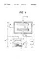
- FIG. 1is a diagram partly in section showing the construction of an apparatus for removing foreign particles which adhere to a wafer by employing a plasma according to the present invention
- FIG. 2is a diagram partly in section showing the construction of an etching apparatus wherein foreign particles adhering to a wafer are removed before an etching process by applying this invention to the etching device;
- FIG. 3is a diagram partly in section showing an embodiment wherein this invention is applied to a sputtering apparatus
- FIG. 4is a diagram partly in section showing the construction of an apparatus for removing foreign particles on inner faces of a processing chamber
- FIG. 5is a diagram partly in section showing the construction of an apparatus for removing foreign particles in an atmospheric environment and in a dry atmosphere according to the present invention
- FIG. 6is a diagram partly in section showing a transfer mechanism that is integrated in a dry process device and the construction of an apparatus for removing foreign particles in a vacuum chamber according to the present invention
- FIG. 7is a diagram partly in section showing the construction of another embodiment of an apparatus for removing foreign particles according to the present invention.
- FIG. 8is a plan view showing a system construction in case wherein this invention is applied to a dry process device system.
- FIG. 9is a diagram partly in section showing a model of a vibration system of adhered foreign particles according to the present invention.
- FIG. 1is a diagram showing an embodiment of a method of removing foreign particles and its apparatus according to the present invention, wherein numeral 1 designates a vacuum chamber, numeral 2 designates a stage, numeral 3 designates a counter electrode, numerals 4a and 4b designate electrodes for removing foreign particles, numeral 5 designates an insulating layer, numerals 6a, 6b, 6c and 6d designate insulating materials, numeral 7 designates a signal generator, numeral 8 designates an RF amplifier, numeral 9 designates a resistor, numeral 10 designates a capacitor, numerals 11 and 12 designate DC power supplies, numerals 13a and 13b designate magnets, numeral 14 designates a core, numeral 15 designates a magnetic field, numeral 16 designates an RF power supply for generating a plasma, numeral 17 designates a filter, and numeral 18 designates a wafer.
- numeral 1designates a vacuum chamber
- numeral 2designates a stage
- the stage 2 coated with the thin insulating layer 5 on its surface and the counter electrode 3 for generating a plasmaare opposedly provided in the vacuum chamber 1, and a couple of electrodes 4a and 4b for removing foreign particles are provided between the stage 2 and the counter electrode 3.
- the wafer 18 for forming a fine patternis mounted on the insulating film 5 of the stage 2.
- the vacuum chamber 1can be supplied with a gas for a plasma processing from a supply source, not shown, and gases in the vacuum chamber 1 can be exhausted by a vacuum generating device, not shown.
- the stage 2is composed of an electrically conductive body, which is installed at the bottom face of the vacuum chamber 1 through the insulating material 6d. Also the counter electrode 3 is installed at the upper face of the vacuum chamber 1 through the insulating material 6a.
- the stage 2is respectively supplied with an RF voltage from the signal generator 7 through the RF amplifier 8 and a positive DC voltage from the DC power supply 11, and the frequency of the RF voltage generated from the signal generator 7 is continuously changed.
- the stage 2is grounded through the capacitor 10 and the resistor 9, such that a matching of the high-frequency amplifier 8 and the load impedance of a plasma can be made also with respect to a change in frequency.
- the insulating layer 5 on the stage 2prevents an electric charge which flows in from the plasma, from flowing to ground and helps electrify the wafer 18 by a voltage applied from the DC power supply 11.
- the counter electrode 3is supplied with an RF voltage of 100 MHz from the RF power supply 16 for generating a plasma, a high-frequency current flows from the counter electrode 3 to among the inner walls of the vacuum chamber, and a plasma is generated.
- the filter 17is connected to the counter electrode 3 so that the impedance between the counter electrode 3 and ground is low with respect to the frequency of the RF voltage applied to the stage 2.
- an RF current due to the RF voltage applied to the stage 2uniformly flows to the counter electrode 3, and, since the impedance is high with respect to the frequency of RF current for generating the plasma, the RF current for generating the plasma does not flow to ground.
- the electrode 4a for removing foreign particlesis supplied with a positive voltage from the DC power supply 12 and the electrode 4b for removing foreign particles is applied with a negative voltage of the DC power supply 12.
- These electrodes 4a and 4b for removing foreign particlesare attached to inner walls of the vacuum chamber 1 respectively through the insulating materials 6c and 6b.
- Magnetic field generating meanscomposed of couples of magnets 13a and 13b, which surround the end portions of the electrode 4a for removing foreign particles, and the core 14, are provided at both end portions of the electrode 4a for removing foreign particles.
- the electrode 4a for removing foreign particles and the magnetic field generating meansare disposed on the side of the stage 2, these elements may be disposed on the side of the counter electrode 3. In the following explanation, these electrodes 4a and 4b for removing foreign particles are disposed as illustrated.
- the wafer 18is mounted on the stage 2 and a constant amount of a gas is supplied to the vacuum chamber 1 from a gas supply source for plasma processing, not shown. If the gas is only for removing the foreign particles, an inert gas such as argon gas is used.
- the gasis exhausted by a vacuum generating device, not shown, the inside of the vacuum chamber 1 is maintained at a vacuum of approximately 1 Pa, and a plasma is generated in the vacuum chamber 1 by supplying a high-frequency power from the RF power supply 16 for generating a plasma at the counter electrode 3.
- a positive DC voltageis applied on the stage 2 from the DC power supply 11, and a negative charge flows from the plasma, whereby the surface of the wafer is electrified and also the foreign particles adhering to the surface of the wafer are negatively electrified.
- the frequency of the RF voltage outputted from the signal generator 7is continuously changed from 1 kHz to 50 MHz, amplified by the RF amplifier 8 and is applied to the stage 2.
- a sheath(spatial charge layer) is formed between the plasma generated by the counter electrode 3 and the surface of the wafer 18, and a high-frequency electric field is generated at the sheath by the RF voltage applied on the stage 2.
- a direct current electric fieldis synthesized in this high-frequency electric field which is caused by a difference in speeds of movement of electrons and ions, and the foreign particles on the wafer 18, which are negatively electrified by the electric field, are subject to a force for separating the foreign particles from the wafer, which force is strengthened or weakened by changes in the frequency of the high-frequency wave, and so the foreign particles are subject to a vibration by the changing force.
- the foreign particles on the wafer 18are drawn to the wafer by a force, such as van der Waal's force, and that a kind of vibration system is formed by the separating force, mentioned above.
- a forcesuch as van der Waal's force
- a kind of vibration systemis formed by the separating force, mentioned above.
- the plurality of frequenciesare the original frequency and the modulated frequency. Further, the same effect can be achieved by applying a radio wave which is FM-modulated.
- the vibration systems formed by the foreign particles on the wafer 18are respectively provided with different periods of vibration. Accordingly, the vibration energy is enhanced for each of the foreign particles having a different period of vibration by continuously changing the frequency of the RF voltage applied to the stage 2, or by applying a plurality of thereto, thereby separating it from the surface of the wafer 18. In this way, more foreign particles can be removed by changing the frequencies, and defects caused by the foreign particles on the surface of the wafer can be reduced. Further, the continuous changing of the RF voltage and the process of setting a plurality of frequencies may be performed once, they may be repeatedly performed for a plural number of times.
- the foreign particles separated from the wafer 18enter the plasma by being drawn to the electric field of the sheath. Since the electron temperature of the discharge plasma is considerably high compared with the ion temperature, the foreign particles in the plasma are negatively electrified such that the charge amounts incident on the surface of the foreign particles are equivalent. Also, with respect to a sheath formed between the plasma and the electrode or the inner wall of the vacuum chamber, an electric field is formed from the plasma in the direction toward the wall face based on the same principle. This electric field operates to reduce the flowing-away of electrons. Therefore, the negatively electrified foreign particles can not come out of the plasma due to this electric field, so they float in the vicinity of the sheath of the plasma.
- a magnetic fieldis formed in parallel to the surface of the electrode 4a for removing foreign particles using the magnets 13a and 13b and the core 14, and electrons in the plasma are restrained by the magnetic field. Therefore, a flowing-in of electrons to the electrode 4a for removing foreign particles is considerably reduced. Further, an electric field is formed in the direction of drawing the negatively electrified foreign particles to the side of the electrode 4a for removing foreign particles, at the sheath on the surface of the electrode 4a for removing foreign particles by applying a positive voltage on the electrode 4a and a negative voltage on the electrode 4b for removing foreign particles, from the DC power supply 12. As a result, the foreign particles are adsorbed onto the electrode 4a by this electric field.
- a very weak electric fieldis formed in the plasma by the DC voltage applied between the electrodes 4a and 4b for removing foreign particles, and the negatively electrified foreign particles in the plasma move toward the electrode 4a by this electric field, and are adsorbed as described above.
- a processing gassuch as an etching gas, a CVD gas or the like into the vacuum chamber 1, and to continuously perform a dry process such as an etching or a CVD, after removing the foreign particles. It is also possible to take out the wafer from the vacuum chamber 1 and to perform the processing in another chamber. Further, an explanation has been given to this embodiment centering on the removing of foreign particles by an inert gas. However, the removing process can be performed in combination with a processing, such as a dry etching process. The foreign particles are removed from the wafer using the same method as explained in this embodiment, by introducing an etching gas, and are taken in the plasma.
- a processing gassuch as an etching gas, a CVD gas or the like
- the high-frequency bias condition applied on the stage 2is equal to that in a normal etching process, and the etching is performed.
- a process having no influence of the foreign particlescan be performed, since the foreign particles which have been taken in to the plasma are adsorbed to the electrode 4a for removing foreign particles and are removed.
- the waferis taken out from the vacuum chamber 1, a plasma is generated, the polarity of the DC power supply 12 is switched, a positive voltage is applied on the electrode 4a for removing foreign particles and a negative voltage is applied on the electrode 4b for removing foreign particles.
- O 2 , CF 4 and Cl 2are successively introduced into the vacuum chamber 1 as cleaning gases, and ions and radicals of these are generated and are incident on the surface of the electrode 4a for removing foreign particles.
- the magnetic fieldsare formed on the surface of the electrode 4a for removing foreign particles as mentioned above, these ions and radicals receive almost no influence from the magnetic fields.
- the ionsare accelerated by the electric field of the sheath formed on the surface of the electrode 4a and are incident thereon, and these ions react with the foreign particles adsorbed on the surface along with the radicals, gasify them, and the reacted gases are discharged from the vacuum chamber, thereby performing a cleaning.
- the foreign particles which have adhered to the wafer 18are removed and are discharged from the vacuum chamber 1 by the above continuous processing.
- the removing of the foreign particles on the surface of the wafercan be performed by turning over the wafer and mounting it on the stage 2.
- sulfur hexafluoride gasis used as a cleaning gas, even the foreign particles embedded in the wafer can readily be removed since the surface of the silicon wafer is isometrically etched by generated fluorine radicals, by which the prevention of contamination in a diffusing furnace or the like can be achieved.
- FIG. 2is a diagram showing another embodiment of a method of removing foreign particles and its apparatus according to the present invention, wherein numeral 19 designates a quartz window, numeral 20 designates a cavity resonator, and numeral 21 designates a slot antenna.
- numeral 19designates a quartz window
- numeral 20designates a cavity resonator
- numeral 21designates a slot antenna.
- the elements corresponding to those in FIG. 1are given the same notation and a duplicate explanation thereof will be omitted.
- the cavity resonator 20is provided instead of the counter electrode 3 in the embodiment shown in FIG. 1.
- the quartz window 19is installed on a wall face of the vacuum chamber 1 opposing the stage 2, and the cavity resonator 20 having the slot antenna 21 is installed in juxtaposition with the quartz window, such that the slot antenna 21 is directed to the quartz window 19.
- a plasma processing gasis introduced into the vacuum chamber 1, a vacuum state of approximately 1 Pa is maintained, and the stage 2 is supplied with an RF voltage, at a frequency which continuously changes, from signal generator 7 via the RF amplifier 8, and a positive DC voltage from the DC power supply 11.
- a microwaveis supplied to the cavity resonator 20 from a microwave supply source, not shown.
- the quartz window 19maintains a vacuum in the vacuum chamber 1 and the microwave can be radiated from the slot antenna 21 to the vacuum chamber 1.
- An aluminum layeris formed on the surface of the wafer 18 which is mounted on the stage 2, on which a resist mask is formed.
- an etching gas(Cl 2 ) is introduced into the vacuum chamber, which is exhausted by a vacuum generating device, not shown, thereby maintaining the inside of the vacuum chamber 1 at a vacuum of approximately 1 Pa.
- a microwaveis supplied to the cavity resonator 20, which is radiated to the inside of the vacuum chamber 1 by the slot antenna 21, thereby generating a plasma.
- the cavity resonator 20has the function of matching the load of the plasma generated in the vacuum chamber 1 with the microwave, by which the plasma is stabilized.
- a positive DC voltageis supplied to the stage 2 from the DC power supply 11, a negative charge is made to flow from the plasma, and the surface of the wafer 18 is negatively electrified. Therefore, the foreign particles adhering to the surface of the wafer 18 are also negatively electrified.
- an RF voltage having a frequency which continuously changesis applied on the stage 2 as in the embodiment shown in FIG. 1, from the signal generator 7 through the RF amplifier 8.
- a sheathis formed between the plasma and the surface of the wafer 18, and a high-frequency electric field whose frequency changes in accordance with the frequency of the RF voltage, is generated at the sheath by the RF voltage applied to the stage 2.
- a force for separating the foreign particles from the wafer 18is applied thereto by the operation of the high-frequency electric field and the electric charge of the foreign particles.
- the frequency of the high-frequency electric fieldagrees with the natural frequency of each of the adhered foreign particles, each of the foreign particles is separated from the wafer 18.
- the separated foreign particlesfloat in the plasma on the sheath.
- the supply of the microwaveis stopped, and the etching gas is exhausted.
- the foreign particles floating in the plasmaadhere to the surface of the wafer 18 again, with the disappearance of the plasma due to the stoppage of supplying the microwave.
- a patternhas already been formed on the surface.
- the foreign particlescan be removed by a cleaning or the like of the wafer 18 without a negative influence on the pattern.
- FIG. 3designates a target electrode
- numeral 23designates a target
- numerals 24 and 25designate coils
- numeral 26designates a yoke
- numeral 27designates a sputtering power supply
- numeral 28designates a coil power supply
- numeral 29designates a magnetic field
- numerals 30, 31, 32 and 33designate switches
- numeral 34designates an RF power supply.
- the elements corresponding to those in FIG. 1are given the same notation and a duplicated explanation will be omitted.
- the target electrode 22composed of the target 23, the coils 24 and 25 and the yoke 26 is installed at an opening of the vacuum chamber opposite to the stage 2, in FIG. 3.
- the target electrode 22is insulated from the wall face of the vacuum chamber 1 through the insulating materials 6e and 6f.
- the coils 24 and 25are connected to the coil power supply 28.
- the sputtering power supply 7is connected to the target electrode 22 through the switch 30. Further, the switch 31 selects either one of connecting three states including (a) connecting the stage 2 to ground, (b) connecting the stage 2 to the RF amplifier 8, the capacitor 10 and the DC power supply 11, and (c) connecting the stage 2 to the RF power supply 34, which is itself connectable to the target electrode 22 through the switch 33.
- a cleaning gasis introduced into the processing chamber 1, and RF power is supplied to the stage 2 from the RF power supply 34 through the switch 31 by which a plasma is generated.
- the switch 30is turned off open and the coil power supply 28 is not operated.
- the switch 33is turned on closed , and an RF voltage, which is outputted from the RF amplifier 8 through the switch 32 and at a frequency which continuously changes, and a DC voltage, from the DC power supply 11, are supplied to the target electrode 22.
- An electric field having a frequency in accordance with the change of the frequency of the RF voltage from the RF amplifier 8is generated at the sheath between the plasma and the surface of the target 23.
- the RF voltage of the RF power supply 34is applied to the target electrode 22 by the switches 32 and 33 thereby generating a plasma, and the RF voltage which is outputted from the RF amplifier 8 by the switch 31 and which has a frequency which continuously changes, and the DC voltage of the DC power supply 11, are applied to the stage 2, by which the foreign particles on the wafer 18 can be removed by the same operation as in the preceding embodiment.
- the foreign particles floating in the plasmacan naturally be removed by the electrodes for removing the foreign particles and the magnetic field generating means.
- the switch 33is turned off opened, and the stage 2 is connected to ground by the switch 31.
- the foreign particles on the wafer 18 and target 23are removed, and the film forming can be performed without being negatively influenced by the foreign particles.
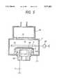
- FIG. 4is a diagram showing another embodiment of a method of removing foreign particles and its apparatus according to the present invention, wherein numeral 35 designates a ground electrode, numeral 36 designates an RF power supply, numeral 37 designates an LFP (low pass filter), and numeral 38 designates a switch.
- numeral 35designates a ground electrode
- numeral 36designates an RF power supply
- numeral 37designates an LFP (low pass filter)
- numeral 38designates a switch.
- the elements corresponding to those in FIG. 1are given the same notation and a duplicate explanation thereof will be omitted.
- This embodimentis for removing foreign particles or layers apt to be stripped off which adhere to the inner wall face of the vacuum chamber 1 in a wafer processing, such as an etching or a CVD processing.
- the RF power supply 36 and the LFP 37are connected to the stage 2.
- the ground electrode 35is attached to the vacuum chamber 1 opposite to the stage 2 such that the ground electrode is insulated from the inner wall of the vacuum chamber.
- the switch 38selects between a state of grounding the vacuum chamber 1 and a state of connecting the vacuum chamber 1 to the RF amplifier 8, the capacitor 10 and the DC power supply 11.
- argon gas or the likeis employed for cleaning.
- a gas for etching the adhered layersuch as ethylene fluoride gas, which can be used along with an etching gas.
- the cleaning gasis discharged from the inside of the vacuum chamber 1, and the operation proceeds to a wafer processing such as an etching or a CVD, thereby making it possible to reduce the influence produced by the foreign particles.
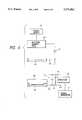
- FIG. 5is a diagram showing another embodiment of a method of removing foreign particles and its device according to the present invention.
- Numeral 40designates an RF power supply of 13.56 MHz
- numeral 41designates a ring-like electrode
- numeral 42designates a high-frequency vibration source generating a variable vibration frequency.
- the elements corresponding to those in FIG. 2are given the same notation and a duplicate explanation thereof will be omitted.
- This embodimentis for avoiding damage to an element formed on the surface of the wafer 18 by ion bombardment etc. during cleaning of the wafer 18.
- the ring-like electrode 41is installed in surrounding relationship to the stage 2 in the vacuum chamber 1, and the RF power supply 40 is connected thereto.
- the stage 2is connected to the high-frequency vibration source 42, which vibrates at a frequency of from 100 kHz to 50 MHz, by which the wafer on the stage 2 can be vibrated.
- a vacuum state of approximately 1 Pais maintained, and a microwave is supplied to the cavity resonator 20 from a microwave supply source, not shown, thereby generating a plasma in the vacuum chamber 1.
- the stage 2is supplied with a positive DC voltage from the DC power supply 11 and also the wafer 18 on the stage 2 is vibrated by the high-frequency vibration source 42 with a continuously changing frequency.
- the surface of the wafer 18is electrified by the applied DC voltage, and the foreign particles adhering to the surface are simultaneously electrified and receive a force for separating them from the surface of the wafer by an electric field of a plasma potential generated at the sheath between the plasma and the wafer 18.
- the wafer 18is vibrated at a high frequency under this state, the foreign particles on the surface of the wafer 18 receive a separating force which is due to the acceleration produced by the vibration, while also being subjected to a separating force due to the electric field.
- the vibration of the foreign particlesincreases by continuously changing the vibration frequency and by matching the frequency with the vibration frequency of each of the adhered foreign particles, and so the foreign particles are separated from the surface of the wafer and are taken into the plasma.
- the voltage applied to the wafer 18is only the voltage of the plasma potential, and therefore, there is no damage to the wafer 18 by ion bombardment etc.
- a high-frequency waveis supplied to the ring-like electrode 41 from the RF power supply 40 thereby generating a plasma at the surrounding area the ring-like electrode 41, and the supply of the microwave is gradually reduced.
- the plasma generated on the stage 2gradually disappears and there is only the ring-like plasma generated at the surrounding area of the ring-like electrode 41.
- the foreign particles which have been taken in the plasmamove along with the plasma, and are enclosed in the plasma at the surrounding area of the ring-like electrode 41.
- the plasmadisappears and the foreign particles drop at the surrounding area of the stage 2.
- the surrounding area of the stage 2is made an exhaust port, and a cleaning gas is made flow, so that the foreign particles can be discharged more efficiently.
- a natural oxide layer on the surface of the wafer 18 or the likeis removed by the cleaning gas simultaneously with the foreign particle removing operation.
- the contamination removing operation and the foreign particle removing operationcan be performed with a low damage.
- FIG. 6is a diagram showing another embodiment of a method of removing foreign particles and its apparatus according to the present invention, wherein numeral 43 designates an electron shower head, numeral 44 designates its power supply, numeral 45 designates an arm of a transfer system, and numeral 46 designates a removing electrode.
- numeral 43designates an electron shower head
- numeral 44designates its power supply
- numeral 45designates an arm of a transfer system
- numeral 46designates a removing electrode.
- the elements corresponding to those in FIG. 1are given the same notation and a duplicate explanation thereof will be omitted.
- the electron shower head 43, the transfer arm 45 and the removing electrode 46are disposed in a vacuum chamber, not shown, having a vacuum atmosphere of from 0.01 to 1 Pa.
- This embodimentis for removing foreign particles at a transfer mechanism which is integrated with a dry process device and is provided in a vacuum chamber.
- the electron shower head 43 and the removing electrode 46are installed above a position under which the transfer arm 45 moves.
- the transfer arm 45is drifting in view of a direct current potential supplied by the capacitor 10.
- a negative DC voltageis applied to the electron shower 43 from the DC power supply 11, and the removing electrode 46 is supplied with a positive DC voltage from the DC power supply 11, and also with an RF voltage having a frequency which continuously changes from the RF amplifier 8 while performing a matching by the capacitor 10 and the resistor 9.
- the transfer arm 45is moved under the electron shower head 43, the electron shower head 43 is operated, and at the same time a negative DC voltage of 500 V is applied to the transfer arm 45 from the DC power supply 11 by which the transfer arm 45 is electrified to 500 V. At this moment, the foreign particles adhered to the transfer arm 45 are also electrified.
- the transfer arm 45is moved under the foreign particle removing electrode 46, the distance between the removing electrode 46 and the transfer arm 45 being as near as 1 mm, and the removing electrode 46 is supplied with the RF voltage having a frequency which continuously changes as supplied from the RF amplifier 8, and the positive DC voltage from the DC power supply 11.
- the foreign particles on the surface of the transfer arm 45are subjected to a force drawing them to the removing electrode 46 and a vibrating force by an electric field which is formed between the removing electrode 46 and the transfer arm 45.
- the vibration of each of the foreign particlesincreases, and the foreign particles are removed from the transfer arm 45 and are adsorbed by the removing electrode 46.
- the transfer mechanism and the vacuum chamberare cleaned, the adhesion of the foreign particles to a wafer can be reduced and a processing with little influence by the foreign particles can be achieved.
- FIG. 7is a diagram showing another embodiment of a method of removing foreign particles and its apparatus according to the present invention, wherein numeral 47 designates a counter removing electrode, numeral 48 designates a stage electrode, numeral 49 designates an ion generator, and numerals 50 and 51 designate change-over switches.
- numeral 47designates a counter removing electrode
- numeral 48designates a stage electrode
- numeral 49designates an ion generator
- numerals 50 and 51designate change-over switches.
- the elements corresponding to those in FIG. 1are given the same notation and a duplicate explanation thereof will be omitted.
- the counter removing electrode 47, the stage electrode 48 and the ion generator 49are disposed in an oxygen environment under an atmospheric pressure.
- This embodimentis for removing foreign particles from a wafer, using a transfer mechanism and the like under an atmospheric pressure environment that does not require a vacuum chamber.
- the insulating layer 5is coated on the surface of the stage electrode 48, on which the wafer 18 is mounted opposite to the counter electrode 47.
- the stage electrode 48 and the counter electrode 47are supplied with a DC voltage from the DC power supply 11 through the change-over switches 50 and 51, and also an RF voltage having a frequency which continuously changes as supplied from the RF amplifier 8, while performing a matching by the capacitor 10 and the resistor 9. Further, ions generated from the ion generator 49 are supplied between both electrodes.
- the wafer 18is mounted on the stage electrode 48, a negative polarity is connected to the counter electrode 47 and the ion generator 49 by the change-over switches 50 and 51, a positive polarity is connected to the stage electrode 48 and a DC voltage of 500 V is applied thereto. Negative ions are generated from the ion generator 49, by which the surface of the wafer 18 and the foreign particles adhering to the surface are negatively electrified.
- the positive polarityis connected to the counter electrode 47 by switching the change-over switches 50 and 51, the negative polarity is connected to the stage electrode 48, and a DC voltage of 800 V and an RF voltage having a frequency which continuously changes as supplied from the RF amplifier 8, are applied thereto.
- the foreign particles on the wafer 18are separated according to the same principle as in the embodiment of FIG. 6, and are adsorbed onto the counter electrode 47.
- the same effectcan be achieved not only in a vacuum, but also under an atmospheric pressure environment.
- a waferis adsorbed to a rotating disk which is rotated at a high speed, whereby a centrifugal force is applied on foreign particles which have adhered to the wafer.
- the rotating diskis vibrated by a vibrator, and further the frequency of vibration is gradually changed.
- the foreign particlescan be separated from the wafer and removed when the vibration frequency of the vibrator is equal to the resonant frequency of each of the foreign particles.
- the foreign particles on the wafercan be removed in a dry atmosphere and a vacuum atmosphere. Therefore, the processing, in conjunction with an etching device or a film forming device, is facilitated, and the foreign particles can be removed from the inside of a processing chamber and from portions having a possibility of becoming a foreign particle generating source, by which a processing with little dust generation can be performed.
- FIG. 8is a diagram showing another embodiment of a method of removing foreign particles and its apparatus according to the present invention, wherein numeral 52 designates a dry cleaning chamber, numeral 53 designates a charge and discharge chamber, numeral 54 designates a foreign particle removing and light etching chamber, numeral 55 designates a CVD deposition chamber, numeral 56 designates an arm cleaning chamber, numeral 57 designates a sputtering deposition chamber, numeral 58 designates gate valves, numeral 59 designates a transfer chamber and numeral 60 designates a transfer robot.
- numeral 52designates a dry cleaning chamber
- numeral 53designates a charge and discharge chamber
- numeral 54designates a foreign particle removing and light etching chamber
- numeral 55designates a CVD deposition chamber
- numeral 56designates an arm cleaning chamber
- numeral 57designates a sputtering deposition chamber
- numeral 58designates gate valves
- numeral 59designates a transfer chamber
- the transfer chamber 59is disposed at the central position of the apparatus at which center position the transfer robot 60 is installed, the construction can connect the respective processing chambers way of the gate valves 58 and five chambers are provided in the surrounding portion of the transfer chamber 59.
- the first chamberis the charge and discharge chamber 53 in front of which the dry cleaning chamber 52 having a foreign particle removing means under an atmospheric environment shown in FIG. 7 is provided.
- the chamber 52removes foreign particles adhering to the surface of a transferred wafer and foreign particles adhering to the back face thereof, and prevents foreign particles from carrying over to the inside of the apparatus through the wafers.
- the waferis transferred to the vacuum transfer chamber 59 by the robot arm 60 through the charge and discharge chamber 53.
- the waferis transferred to the foreign particle removing and light etching chamber shown in FIG. 5, wherein the foreign particles on the surface of the wafer are again removed and a contaminated layer on the surface is removed.
- the waferis transferred by the transfer robot 60 to the sputtering deposition chamber 57 having a cleaning mechanism shown in FIG. 3, wherein a tungsten layer is sputtered.
- a portion thereof for mounting the waferis periodically taken into the arm cleaning chamber 56, wherein the foreign particles are removed from the surface so that the foreign particles do not adhere to the transferring wafer.
- the arm cleaning chamber 56is provided with the electron shower head 43 and the removing electrode 46, whereby the cleaning is performed by the method as explained in the preceding embodiment.
- the waferis transferred to the CVD deposition chamber 55, wherein another tungsten layer is formed by the CVD process. Thereafter, the wafer is taken out from the wafer vacuum chamber through the charge and discharge chamber 53, and the process is completed by removing the foreign particles on the front face and the back face of the wafer in the dry cleaning chamber 52.
- the foreign particlesare removed before and after the dry process thereby preventing the generation of defects by the foreign particles and preventing the foreign particles from being carried to a successive step.
- the control of the foreign particlescan certainly be performed by installing an in-line foreign particle inspection device before the dry cleaning chamber 52, and so a further stable production can be performed.
- the foreign particle removing device under the atmospheric environment shown in FIG. 7is attached to a wafer stage of an exposure device, by which foreign particles on the surface of the stage and foreign particles on an exposed wafer can be removed.
- any foreign particles adhering to a substrate, such as a wafer, that is an object of an etching or a film forming process, so inner wall faces of a processing chamber and, an object in the processing chamber such as a target for film forming,can be removed.
- the substratecan be rendered in a state without the adherence of foreign particles and a state wherein separated foreign particles do not again adhere thereto, and an etching step or a film forming step can be performed in succession to the foreign particle removing process while the wafer remains as treated by the foreign particle removing process.
- the exposure stepcan successively be performed, thereby reducing operational steps, achieving a promotion in product yield in the production of semiconductor devices and promoting the productivity.
Landscapes
- Chemical & Material Sciences (AREA)
- Engineering & Computer Science (AREA)
- Physics & Mathematics (AREA)
- Chemical Kinetics & Catalysis (AREA)
- Organic Chemistry (AREA)
- Metallurgy (AREA)
- Mechanical Engineering (AREA)
- Materials Engineering (AREA)
- Condensed Matter Physics & Semiconductors (AREA)
- Microelectronics & Electronic Packaging (AREA)
- Power Engineering (AREA)
- Computer Hardware Design (AREA)
- Manufacturing & Machinery (AREA)
- General Physics & Mathematics (AREA)
- General Chemical & Material Sciences (AREA)
- Analytical Chemistry (AREA)
- Plasma & Fusion (AREA)
- Drying Of Semiconductors (AREA)
- Cleaning Or Drying Semiconductors (AREA)
- ing And Chemical Polishing (AREA)
Abstract
Description
Claims (23)
Applications Claiming Priority (2)
| Application Number | Priority Date | Filing Date | Title |
|---|---|---|---|
| JP17806793 | 1993-07-19 | ||
| JP5-178067 | 1993-07-19 |
Publications (1)
| Publication Number | Publication Date |
|---|---|
| US5531862Atrue US5531862A (en) | 1996-07-02 |
Family
ID=16042040
Family Applications (1)
| Application Number | Title | Priority Date | Filing Date |
|---|---|---|---|
| US08/277,017Expired - LifetimeUS5531862A (en) | 1993-07-19 | 1994-07-19 | Method of and apparatus for removing foreign particles |
Country Status (2)
| Country | Link |
|---|---|
| US (1) | US5531862A (en) |
| KR (1) | KR0141659B1 (en) |
Cited By (76)
| Publication number | Priority date | Publication date | Assignee | Title |
|---|---|---|---|---|
| WO1996038311A1 (en)* | 1995-06-02 | 1996-12-05 | The University Of Tennessee Research Corporation | Method and apparatus for cleaning surfaces with a glow discharge plasma at one atmosphere of pressure |
| WO1997034450A1 (en)* | 1996-03-12 | 1997-09-18 | The Regents Of The University Of California | Particulate contamination removal from wafers using plasmas and mechanical agitation |
| US5686050A (en) | 1992-10-09 | 1997-11-11 | The University Of Tennessee Research Corporation | Method and apparatus for the electrostatic charging of a web or film |
| EP0790642A3 (en)* | 1996-02-02 | 1998-04-01 | Applied Materials, Inc. | Method and apparatus for removing contaminant particles from surfaces in semiconductor processing equipment |
| US5795399A (en)* | 1994-06-30 | 1998-08-18 | Kabushiki Kaisha Toshiba | Semiconductor device manufacturing apparatus, method for removing reaction product, and method of suppressing deposition of reaction product |
| US5863339A (en)* | 1995-12-15 | 1999-01-26 | Nec Corporation | Chamber etching of plasma processing apparatus |
| US5895558A (en) | 1995-06-19 | 1999-04-20 | The University Of Tennessee Research Corporation | Discharge methods and electrodes for generating plasmas at one atmosphere of pressure, and materials treated therewith |
| WO1999036276A1 (en)* | 1998-01-16 | 1999-07-22 | Etex Corporation | Surface modification of medical implants |
| US5950071A (en)* | 1995-11-17 | 1999-09-07 | Lightforce Technology, Inc. | Detachment and removal of microscopic surface contaminants using a pulsed detach light |
| US5955174A (en) | 1995-03-28 | 1999-09-21 | The University Of Tennessee Research Corporation | Composite of pleated and nonwoven webs |
| US5961850A (en)* | 1995-03-20 | 1999-10-05 | Hitachi, Ltd. | Plasma processing method and apparatus |
| US6024105A (en)* | 1997-08-07 | 2000-02-15 | Mitsubishi Denki Kabushiki Kaisha | Semiconductor manufacturing device and method of removing particles therefrom |
| US6158383A (en)* | 1919-02-20 | 2000-12-12 | Hitachi, Ltd. | Plasma processing method and apparatus |
| US6187160B1 (en)* | 1998-06-19 | 2001-02-13 | Leybold Systems Gmbh | Apparatus for the coating of substrates in a vacuum chamber |
| US6195834B1 (en) | 1999-03-25 | 2001-03-06 | David Shteingold | Method and apparatus for removing foreign particles |
| US6250250B1 (en)* | 1999-03-18 | 2001-06-26 | Yuri Maishev | Multiple-cell source of uniform plasma |
| WO2002007926A1 (en)* | 2000-07-24 | 2002-01-31 | Florida State University Research Foundation | Method and apparatus for removing minute particles from a surface |
| US6390019B1 (en)* | 1998-06-11 | 2002-05-21 | Applied Materials, Inc. | Chamber having improved process monitoring window |
| US6478924B1 (en)* | 2000-03-07 | 2002-11-12 | Applied Materials, Inc. | Plasma chamber support having dual electrodes |
| WO2002099838A1 (en)* | 2001-06-04 | 2002-12-12 | Applied Materials, Inc. | Particle contamination cleaning from substrates using plasmas, reactive gases, and mechanical agitation |
| US20030003758A1 (en)* | 2001-06-11 | 2003-01-02 | Tsuyoshi Moriya | Method of manufacturing semiconductor devices and semiconductor manufacturing apparatus |
| US20030037801A1 (en)* | 2001-08-27 | 2003-02-27 | Applied Materials, Inc. | Method for increasing the efficiency of substrate processing chamber contamination detection |
| US20030040193A1 (en)* | 2001-08-27 | 2003-02-27 | Applied Materials, Inc. | Method for enhancing substrate processing |
| US20030037800A1 (en)* | 2001-08-27 | 2003-02-27 | Applied Materials, Inc. | Method for removing contamination particles from substrate processing chambers |
| US6564810B1 (en)* | 2000-03-28 | 2003-05-20 | Asm America | Cleaning of semiconductor processing chambers |
| US20030094625A1 (en)* | 1996-01-19 | 2003-05-22 | Semiconductor Energy Laboratory Co., Ltd. | Semiconductor device and method for fabricating the same |
| US6626185B2 (en) | 1996-06-28 | 2003-09-30 | Lam Research Corporation | Method of depositing a silicon containing layer on a semiconductor substrate |
| US20030197501A1 (en)* | 1998-12-18 | 2003-10-23 | Fujitsu Limited | Contactor for semiconductor devices, a testing apparatus using such contactor, a testing method using such contactor, and a method of cleaning such contactor |
| US20030201185A1 (en)* | 2002-04-29 | 2003-10-30 | Applied Materials, Inc. | In-situ pre-clean for electroplating process |
| US6673199B1 (en) | 2001-03-07 | 2004-01-06 | Applied Materials, Inc. | Shaping a plasma with a magnetic field to control etch rate uniformity |
| US6676800B1 (en) | 2000-03-15 | 2004-01-13 | Applied Materials, Inc. | Particle contamination cleaning from substrates using plasmas, reactive gases, and mechanical agitation |
| US6684523B2 (en) | 2001-08-27 | 2004-02-03 | Applied Materials, Inc. | Particle removal apparatus |
| US20040037971A1 (en)* | 2000-04-27 | 2004-02-26 | Toru Otsubo | Plasma processing apparatus and processing method |
| US6725564B2 (en) | 2001-08-27 | 2004-04-27 | Applied Materials, Inc. | Processing platform with integrated particle removal system |
| US20040108503A1 (en)* | 1996-01-19 | 2004-06-10 | Semiconductor Energy Laboratory Co., Ltd. | Semiconductor device and method of fabricating same |
| US6779226B2 (en) | 2001-08-27 | 2004-08-24 | Applied Materials, Inc. | Factory interface particle removal platform |
| US20040177927A1 (en)* | 2001-07-10 | 2004-09-16 | Akihiro Kikuchi | Plasma procesor and plasma processing method |
| US6794311B2 (en) | 2000-07-14 | 2004-09-21 | Applied Materials Inc. | Method and apparatus for treating low k dielectric layers to reduce diffusion |
| US6805137B2 (en) | 2001-08-27 | 2004-10-19 | Applied Materials, Inc. | Method for removing contamination particles from substrates |
| US6805751B2 (en) | 2000-07-24 | 2004-10-19 | Alkansas State University | Method and apparatus for removal of minute particles from a surface using thermophoresis to prevent particle redeposition |
| US20040218157A1 (en)* | 2002-12-20 | 2004-11-04 | Asml Netherlands B.V. | Method for cleaning a surface of a component of a lithographic projection apparatus, lithographic projection apparatus, device manufacturing method and cleaning system |
| US6831742B1 (en) | 2000-10-23 | 2004-12-14 | Applied Materials, Inc | Monitoring substrate processing using reflected radiation |
| US20050057734A1 (en)* | 2002-12-20 | 2005-03-17 | Asml Netherlands B.V. | Lithographic apparatus, device manufacturing method and device manufactured thereby |
| US20050101154A1 (en)* | 1999-06-18 | 2005-05-12 | Judy Huang | Plasma treatment to enhance adhesion and to minimize oxidation of carbon-containing layers |
| US20050235915A1 (en)* | 2004-04-27 | 2005-10-27 | Ho Yeu-Chuan S | Plasma surface treatment electrode assembly and arrangement |
| US7037811B1 (en)* | 1996-01-26 | 2006-05-02 | Semiconductor Energy Laboratory Co., Ltd. | Method for fabricating a semiconductor device |
| US7045465B2 (en)* | 1998-04-13 | 2006-05-16 | Nec Electronics Corporation | Particle-removing method for a semiconductor device manufacturing apparatus |
| US20060112878A1 (en)* | 2002-12-20 | 2006-06-01 | Lam Research Corporation | System and method for controlling plasma with an adjustable coupling to ground circuit |
| US7056381B1 (en) | 1996-01-26 | 2006-06-06 | Semiconductor Energy Laboratory Co., Ltd. | Fabrication method of semiconductor device |
| US7078727B2 (en) | 1996-01-19 | 2006-07-18 | Semiconductor Energy Laboratory Co., Ltd. | Semiconductor device and its manufacturing method |
| US7135741B1 (en) | 1996-03-17 | 2006-11-14 | Semiconductor Energy Laboratory Co., Ltd. | Method of manufacturing a semiconductor device |
| US20070131244A1 (en)* | 2000-07-24 | 2007-06-14 | Arkansas State University | Method and apparatus for removing minute particles from a surface |
| CN100369213C (en)* | 2004-03-29 | 2008-02-13 | 东京毅力科创株式会社 | Plasma processing device and method thereof |
| US20080180357A1 (en)* | 2007-01-25 | 2008-07-31 | Kawakami Masatoshi | Plasma processing apparatus |
| US20080236629A1 (en)* | 2007-03-30 | 2008-10-02 | Tokyo Electron Limited | Cleaning method for turbo molecular pump |
| US7518288B2 (en) | 1996-09-30 | 2009-04-14 | Akrion Technologies, Inc. | System for megasonic processing of an article |
| US7674695B1 (en)* | 2000-01-22 | 2010-03-09 | Loxley Ted A | Wafer cleaning system |
| US7709837B2 (en) | 1996-01-19 | 2010-05-04 | Semiconductor Energy Laboratory Co., Ltd | Semiconductor device and its manufacturing method |
| US20110177694A1 (en)* | 2010-01-15 | 2011-07-21 | Tokyo Electron Limited | Switchable Neutral Beam Source |
| US20110247995A1 (en)* | 2010-04-13 | 2011-10-13 | Tokai University Educational System | Dry etching method and dry etching apparatus |
| CN102759842A (en)* | 2011-04-26 | 2012-10-31 | 佳能株式会社 | Driving circuit for vibration apparatus |
| US20130192760A1 (en)* | 2012-01-31 | 2013-08-01 | Tokyo Electron Limited | Microwave emitting device and surface wave plasma processing apparatus |
| TWI406334B (en)* | 2007-01-12 | 2013-08-21 | Hitachi High Tech Corp | Plasma processing device |
| US20140209243A1 (en)* | 2013-01-25 | 2014-07-31 | Samsung Electronics Co., Ltd. | Plasma Equipment and Method of Dry-Cleaning the Same |
| US20150017744A1 (en)* | 2013-07-09 | 2015-01-15 | Samsung Display Co., Ltd. | Method of removing particles from a display panel and apparatus for performing the same |
| US20150075566A1 (en)* | 2012-04-25 | 2015-03-19 | Tokyo Electron Limited | Method of controlling adherence of microparticles to substrate to be processed, and processing apparatus |
| US20160056018A1 (en)* | 2013-03-15 | 2016-02-25 | Tokyo Electron Limited | Electric pressure systems for control of plasma properties and uniformity |
| TWI573888B (en)* | 2012-08-09 | 2017-03-11 | 愛發科股份有限公司 | Deposition method and deposition apparatus |
| CN113168088A (en)* | 2018-11-27 | 2021-07-23 | Asml荷兰有限公司 | Diaphragm cleaning equipment |
| US11135622B2 (en)* | 2017-03-14 | 2021-10-05 | Lg Electronics Inc. | Device for cleaning surface using electrowetting element and method for controlling the same |
| US20210327679A1 (en)* | 2009-05-01 | 2021-10-21 | Advanced Energy Industries, Inc. | System, method, and apparatus for ion current compensation |
| CN113690280A (en)* | 2021-08-11 | 2021-11-23 | 深圳市华星光电半导体显示技术有限公司 | Array substrate repairing method and array substrate |
| US11302540B2 (en)* | 2018-01-15 | 2022-04-12 | Samsung Electronics Co., Ltd. | Substrate support device and substrate cleaning device including the same |
| CN114959625A (en)* | 2022-05-20 | 2022-08-30 | 深圳市华星光电半导体显示技术有限公司 | Film coating device and cleaning method thereof |
| US20240055225A1 (en)* | 2009-05-01 | 2024-02-15 | Advanced Energy Industries, Inc. | Apparatus to control ion energy |
| US12354836B2 (en) | 2009-05-01 | 2025-07-08 | Advanced Energy Industries, Inc. | System, method, and apparatus for controlling ion energy distribution in plasma processing systems |
Families Citing this family (4)
| Publication number | Priority date | Publication date | Assignee | Title |
|---|---|---|---|---|
| KR100460800B1 (en)* | 1997-07-03 | 2005-05-19 | 삼성전자주식회사 | Plasma treatment apparatus and its residue removal plate manufacturing method |
| KR100789451B1 (en)* | 2001-08-11 | 2008-01-02 | 엘지.필립스 엘시디 주식회사 | Substrate cleaning device and cleaning method |
| KR100771005B1 (en)* | 2006-02-15 | 2007-10-30 | 주식회사 에스에프에이 | Chemical Vapor Deposition Equipment for Flat Panel Displays |
| KR100817415B1 (en)* | 2006-12-05 | 2008-03-27 | 동부일렉트로닉스 주식회사 | Semiconductor device and manufacturing method thereof |
Citations (5)
| Publication number | Priority date | Publication date | Assignee | Title |
|---|---|---|---|---|
| JPH03147317A (en)* | 1989-10-23 | 1991-06-24 | Internatl Business Mach Corp <Ibm> | Method for suppressing contamination in plasma treatment |
| JPH03153885A (en)* | 1989-09-26 | 1991-07-01 | Applied Materials Inc | Method and apparatus for reducing particle contamination of wafers |
| JPH0547712A (en)* | 1991-08-12 | 1993-02-26 | Hitachi Ltd | Plasma processing method and plasma processing apparatus |
| US5247954A (en)* | 1991-11-12 | 1993-09-28 | Submicron Systems, Inc. | Megasonic cleaning system |
| US5377709A (en)* | 1992-10-22 | 1995-01-03 | Shibano; Yoshihide | Ultrasonic vibrator device for ultrasonically cleaning workpiece |
- 1994
- 1994-07-18KRKR1019940017290Apatent/KR0141659B1/ennot_activeExpired - Fee Related
- 1994-07-19USUS08/277,017patent/US5531862A/ennot_activeExpired - Lifetime
Patent Citations (5)
| Publication number | Priority date | Publication date | Assignee | Title |
|---|---|---|---|---|
| JPH03153885A (en)* | 1989-09-26 | 1991-07-01 | Applied Materials Inc | Method and apparatus for reducing particle contamination of wafers |
| JPH03147317A (en)* | 1989-10-23 | 1991-06-24 | Internatl Business Mach Corp <Ibm> | Method for suppressing contamination in plasma treatment |
| JPH0547712A (en)* | 1991-08-12 | 1993-02-26 | Hitachi Ltd | Plasma processing method and plasma processing apparatus |
| US5247954A (en)* | 1991-11-12 | 1993-09-28 | Submicron Systems, Inc. | Megasonic cleaning system |
| US5377709A (en)* | 1992-10-22 | 1995-01-03 | Shibano; Yoshihide | Ultrasonic vibrator device for ultrasonically cleaning workpiece |
Non-Patent Citations (2)
| Title |
|---|
| Goree et al., "Particulate Release From Surfaces Exposed to Plasma", J. Vac. Sci. Technol. A10(6), Nov./Dec. 1992, pp. 3540-3544. |
| Goree et al., Particulate Release From Surfaces Exposed to Plasma , J. Vac. Sci. Technol. A10(6), Nov./Dec. 1992, pp. 3540 3544.* |
Cited By (123)
| Publication number | Priority date | Publication date | Assignee | Title |
|---|---|---|---|---|
| US6158383A (en)* | 1919-02-20 | 2000-12-12 | Hitachi, Ltd. | Plasma processing method and apparatus |
| US5686050A (en) | 1992-10-09 | 1997-11-11 | The University Of Tennessee Research Corporation | Method and apparatus for the electrostatic charging of a web or film |
| US5938854A (en)* | 1993-05-28 | 1999-08-17 | The University Of Tennessee Research Corporation | Method and apparatus for cleaning surfaces with a glow discharge plasma at one atmosphere of pressure |
| US5795399A (en)* | 1994-06-30 | 1998-08-18 | Kabushiki Kaisha Toshiba | Semiconductor device manufacturing apparatus, method for removing reaction product, and method of suppressing deposition of reaction product |
| US5961850A (en)* | 1995-03-20 | 1999-10-05 | Hitachi, Ltd. | Plasma processing method and apparatus |
| US5955174A (en) | 1995-03-28 | 1999-09-21 | The University Of Tennessee Research Corporation | Composite of pleated and nonwoven webs |
| AU695099B2 (en)* | 1995-06-02 | 1998-08-06 | University Of Tennessee Research Corporation, The | Method and apparatus for cleaning surfaces with a glow discharge plasma at one atmosphere of pressure |
| WO1996038311A1 (en)* | 1995-06-02 | 1996-12-05 | The University Of Tennessee Research Corporation | Method and apparatus for cleaning surfaces with a glow discharge plasma at one atmosphere of pressure |
| US5895558A (en) | 1995-06-19 | 1999-04-20 | The University Of Tennessee Research Corporation | Discharge methods and electrodes for generating plasmas at one atmosphere of pressure, and materials treated therewith |
| US6059935A (en) | 1995-06-19 | 2000-05-09 | The University Of Tennessee Research Corporation | Discharge method and apparatus for generating plasmas |
| US6416633B1 (en) | 1995-06-19 | 2002-07-09 | The University Of Tennessee Research Corporation | Resonant excitation method and apparatus for generating plasmas |
| US5950071A (en)* | 1995-11-17 | 1999-09-07 | Lightforce Technology, Inc. | Detachment and removal of microscopic surface contaminants using a pulsed detach light |
| US5863339A (en)* | 1995-12-15 | 1999-01-26 | Nec Corporation | Chamber etching of plasma processing apparatus |
| US6099747A (en)* | 1995-12-15 | 2000-08-08 | Nec Corporation | Chamber etching of plasma processing apparatus |
| US7078727B2 (en) | 1996-01-19 | 2006-07-18 | Semiconductor Energy Laboratory Co., Ltd. | Semiconductor device and its manufacturing method |
| US7427780B2 (en) | 1996-01-19 | 2008-09-23 | Semiconductor Energy Laboratory Co., Ltd. | Semiconductor device and method of fabricating same |
| US7709837B2 (en) | 1996-01-19 | 2010-05-04 | Semiconductor Energy Laboratory Co., Ltd | Semiconductor device and its manufacturing method |
| US20040108503A1 (en)* | 1996-01-19 | 2004-06-10 | Semiconductor Energy Laboratory Co., Ltd. | Semiconductor device and method of fabricating same |
| US20030094625A1 (en)* | 1996-01-19 | 2003-05-22 | Semiconductor Energy Laboratory Co., Ltd. | Semiconductor device and method for fabricating the same |
| US7679087B2 (en) | 1996-01-19 | 2010-03-16 | Semiconductor Energy Laboratory Co., Ltd. | Semiconductor active region of TFTs having radial crystal grains through the whole area of the region |
| US7456056B2 (en) | 1996-01-19 | 2008-11-25 | Semiconductor Energy Laboratory Co., Ltd. | Semiconductor device and method for fabricating the same |
| US6033582A (en)* | 1996-01-22 | 2000-03-07 | Etex Corporation | Surface modification of medical implants |
| US6464889B1 (en) | 1996-01-22 | 2002-10-15 | Etex Corporation | Surface modification of medical implants |
| US7141491B2 (en) | 1996-01-26 | 2006-11-28 | Semiconductor Energy Laboratory Co., Ltd. | Method for fabricating a semiconductor device |
| US7056381B1 (en) | 1996-01-26 | 2006-06-06 | Semiconductor Energy Laboratory Co., Ltd. | Fabrication method of semiconductor device |
| US7037811B1 (en)* | 1996-01-26 | 2006-05-02 | Semiconductor Energy Laboratory Co., Ltd. | Method for fabricating a semiconductor device |
| US7422630B2 (en) | 1996-01-26 | 2008-09-09 | Semiconductor Energy Laboratory Co., Ltd. | Fabrication method of semiconductor device |
| EP0790642A3 (en)* | 1996-02-02 | 1998-04-01 | Applied Materials, Inc. | Method and apparatus for removing contaminant particles from surfaces in semiconductor processing equipment |
| WO1997034450A1 (en)* | 1996-03-12 | 1997-09-18 | The Regents Of The University Of California | Particulate contamination removal from wafers using plasmas and mechanical agitation |
| US5849135A (en)* | 1996-03-12 | 1998-12-15 | The Regents Of The University Of California | Particulate contamination removal from wafers using plasmas and mechanical agitation |
| US7135741B1 (en) | 1996-03-17 | 2006-11-14 | Semiconductor Energy Laboratory Co., Ltd. | Method of manufacturing a semiconductor device |
| US6626185B2 (en) | 1996-06-28 | 2003-09-30 | Lam Research Corporation | Method of depositing a silicon containing layer on a semiconductor substrate |
| US7518288B2 (en) | 1996-09-30 | 2009-04-14 | Akrion Technologies, Inc. | System for megasonic processing of an article |
| US8771427B2 (en) | 1996-09-30 | 2014-07-08 | Akrion Systems, Llc | Method of manufacturing integrated circuit devices |
| US8257505B2 (en) | 1996-09-30 | 2012-09-04 | Akrion Systems, Llc | Method for megasonic processing of an article |
| US6024105A (en)* | 1997-08-07 | 2000-02-15 | Mitsubishi Denki Kabushiki Kaisha | Semiconductor manufacturing device and method of removing particles therefrom |
| WO1999036276A1 (en)* | 1998-01-16 | 1999-07-22 | Etex Corporation | Surface modification of medical implants |
| US7045465B2 (en)* | 1998-04-13 | 2006-05-16 | Nec Electronics Corporation | Particle-removing method for a semiconductor device manufacturing apparatus |
| US6712927B1 (en) | 1998-06-11 | 2004-03-30 | Applied Materials Inc. | Chamber having process monitoring window |
| US6835275B1 (en) | 1998-06-11 | 2004-12-28 | Michael N. Grimbergen | Reducing deposition of process residues on a surface in a chamber |
| US6390019B1 (en)* | 1998-06-11 | 2002-05-21 | Applied Materials, Inc. | Chamber having improved process monitoring window |
| US6187160B1 (en)* | 1998-06-19 | 2001-02-13 | Leybold Systems Gmbh | Apparatus for the coating of substrates in a vacuum chamber |
| US6781395B2 (en)* | 1998-12-18 | 2004-08-24 | Fujitsu Limited | Contactor for semiconductor devices, a testing apparatus using such contactor, a testing method using such contactor, and a method of cleaning such contactor |
| US20030197501A1 (en)* | 1998-12-18 | 2003-10-23 | Fujitsu Limited | Contactor for semiconductor devices, a testing apparatus using such contactor, a testing method using such contactor, and a method of cleaning such contactor |
| US6250250B1 (en)* | 1999-03-18 | 2001-06-26 | Yuri Maishev | Multiple-cell source of uniform plasma |
| US6195834B1 (en) | 1999-03-25 | 2001-03-06 | David Shteingold | Method and apparatus for removing foreign particles |
| US20050101154A1 (en)* | 1999-06-18 | 2005-05-12 | Judy Huang | Plasma treatment to enhance adhesion and to minimize oxidation of carbon-containing layers |
| US7144606B2 (en) | 1999-06-18 | 2006-12-05 | Applied Materials, Inc. | Plasma treatment to enhance adhesion and to minimize oxidation of carbon-containing layers |
| US7674695B1 (en)* | 2000-01-22 | 2010-03-09 | Loxley Ted A | Wafer cleaning system |
| US6478924B1 (en)* | 2000-03-07 | 2002-11-12 | Applied Materials, Inc. | Plasma chamber support having dual electrodes |
| US6676800B1 (en) | 2000-03-15 | 2004-01-13 | Applied Materials, Inc. | Particle contamination cleaning from substrates using plasmas, reactive gases, and mechanical agitation |
| US6564810B1 (en)* | 2000-03-28 | 2003-05-20 | Asm America | Cleaning of semiconductor processing chambers |
| US6708700B2 (en) | 2000-03-28 | 2004-03-23 | Asm America | Cleaning of semiconductor processing chambers |
| US20040037971A1 (en)* | 2000-04-27 | 2004-02-26 | Toru Otsubo | Plasma processing apparatus and processing method |
| US6794311B2 (en) | 2000-07-14 | 2004-09-21 | Applied Materials Inc. | Method and apparatus for treating low k dielectric layers to reduce diffusion |
| US20070131244A1 (en)* | 2000-07-24 | 2007-06-14 | Arkansas State University | Method and apparatus for removing minute particles from a surface |
| US7297895B2 (en) | 2000-07-24 | 2007-11-20 | Arkansas State University | Apparatus for removal of minute particles from a surface using thermophoresis to prevent particle redeposition |
| US20050103359A1 (en)* | 2000-07-24 | 2005-05-19 | Arkansas State University | Apparatus for removal of minute particles from a surface using thermophoresis to prevent particle redeposition |
| US6805751B2 (en) | 2000-07-24 | 2004-10-19 | Alkansas State University | Method and apparatus for removal of minute particles from a surface using thermophoresis to prevent particle redeposition |
| WO2002007926A1 (en)* | 2000-07-24 | 2002-01-31 | Florida State University Research Foundation | Method and apparatus for removing minute particles from a surface |
| US6831742B1 (en) | 2000-10-23 | 2004-12-14 | Applied Materials, Inc | Monitoring substrate processing using reflected radiation |
| US6673199B1 (en) | 2001-03-07 | 2004-01-06 | Applied Materials, Inc. | Shaping a plasma with a magnetic field to control etch rate uniformity |
| WO2002099838A1 (en)* | 2001-06-04 | 2002-12-12 | Applied Materials, Inc. | Particle contamination cleaning from substrates using plasmas, reactive gases, and mechanical agitation |
| US8202394B2 (en)* | 2001-06-11 | 2012-06-19 | Renesas Electronics Corporation | Method of manufacturing semiconductor devices and semiconductor manufacturing apparatus |
| US20030003758A1 (en)* | 2001-06-11 | 2003-01-02 | Tsuyoshi Moriya | Method of manufacturing semiconductor devices and semiconductor manufacturing apparatus |
| US8056503B2 (en)* | 2001-07-10 | 2011-11-15 | Tokyo Electron Limited | Plasma procesor and plasma processing method |
| US20120006492A1 (en)* | 2001-07-10 | 2012-01-12 | Tokyo Electron Limited | Plasma processor and plasma processing method |
| US8387562B2 (en)* | 2001-07-10 | 2013-03-05 | Tokyo Electron Limited | Plasma processor and plasma processing method |
| US20040177927A1 (en)* | 2001-07-10 | 2004-09-16 | Akihiro Kikuchi | Plasma procesor and plasma processing method |
| US20130174983A1 (en)* | 2001-07-10 | 2013-07-11 | Tokyo Electron Limited | Plasma processor and plasma processing method |
| US8904957B2 (en)* | 2001-07-10 | 2014-12-09 | Tokyo Electron Limited | Plasma processor and plasma processing method |
| US20150083332A1 (en)* | 2001-07-10 | 2015-03-26 | Tokyo Electron Limited | Plasma processor and plasma processing method |
| US9437402B2 (en) | 2001-07-10 | 2016-09-06 | Tokyo Electron Limited | Plasma processor and plasma processing method |
| US9728381B2 (en)* | 2001-07-10 | 2017-08-08 | Tokyo Electron Limited | Plasma processor and plasma processing method |
| US20030040193A1 (en)* | 2001-08-27 | 2003-02-27 | Applied Materials, Inc. | Method for enhancing substrate processing |
| US20030037801A1 (en)* | 2001-08-27 | 2003-02-27 | Applied Materials, Inc. | Method for increasing the efficiency of substrate processing chamber contamination detection |
| US6725564B2 (en) | 2001-08-27 | 2004-04-27 | Applied Materials, Inc. | Processing platform with integrated particle removal system |
| US6779226B2 (en) | 2001-08-27 | 2004-08-24 | Applied Materials, Inc. | Factory interface particle removal platform |
| US6805137B2 (en) | 2001-08-27 | 2004-10-19 | Applied Materials, Inc. | Method for removing contamination particles from substrates |
| US6684523B2 (en) | 2001-08-27 | 2004-02-03 | Applied Materials, Inc. | Particle removal apparatus |
| US6878636B2 (en) | 2001-08-27 | 2005-04-12 | Applied Materials, Inc. | Method for enhancing substrate processing |
| US20030037800A1 (en)* | 2001-08-27 | 2003-02-27 | Applied Materials, Inc. | Method for removing contamination particles from substrate processing chambers |
| US20030201185A1 (en)* | 2002-04-29 | 2003-10-30 | Applied Materials, Inc. | In-situ pre-clean for electroplating process |
| US7116394B2 (en)* | 2002-12-20 | 2006-10-03 | Asml Netherlands B.V. | Method for cleaning a surface of a component of a lithographic projection apparatus, lithographic projection apparatus, device manufacturing method and cleaning system |
| US20060112878A1 (en)* | 2002-12-20 | 2006-06-01 | Lam Research Corporation | System and method for controlling plasma with an adjustable coupling to ground circuit |
| US20050057734A1 (en)* | 2002-12-20 | 2005-03-17 | Asml Netherlands B.V. | Lithographic apparatus, device manufacturing method and device manufactured thereby |
| US20040218157A1 (en)* | 2002-12-20 | 2004-11-04 | Asml Netherlands B.V. | Method for cleaning a surface of a component of a lithographic projection apparatus, lithographic projection apparatus, device manufacturing method and cleaning system |
| US7095479B2 (en)* | 2002-12-20 | 2006-08-22 | Asml Netherlands B.V. | Lithographic apparatus, device manufacturing method and device manufactured thereby |
| US8518211B2 (en)* | 2002-12-20 | 2013-08-27 | Lam Research Corporation | System and method for controlling plasma with an adjustable coupling to ground circuit |
| CN100369213C (en)* | 2004-03-29 | 2008-02-13 | 东京毅力科创株式会社 | Plasma processing device and method thereof |
| US20050235915A1 (en)* | 2004-04-27 | 2005-10-27 | Ho Yeu-Chuan S | Plasma surface treatment electrode assembly and arrangement |
| TWI406334B (en)* | 2007-01-12 | 2013-08-21 | Hitachi High Tech Corp | Plasma processing device |
| US20080180357A1 (en)* | 2007-01-25 | 2008-07-31 | Kawakami Masatoshi | Plasma processing apparatus |
| US8062432B2 (en)* | 2007-03-30 | 2011-11-22 | Tokyo Electron Limited | Cleaning method for turbo molecular pump |
| US20080236629A1 (en)* | 2007-03-30 | 2008-10-02 | Tokyo Electron Limited | Cleaning method for turbo molecular pump |
| US20240055225A1 (en)* | 2009-05-01 | 2024-02-15 | Advanced Energy Industries, Inc. | Apparatus to control ion energy |
| US12255048B2 (en)* | 2009-05-01 | 2025-03-18 | Advanced Energy Industries, Inc. | Apparatus to control ion energy |
| US12354836B2 (en) | 2009-05-01 | 2025-07-08 | Advanced Energy Industries, Inc. | System, method, and apparatus for controlling ion energy distribution in plasma processing systems |
| US20210327679A1 (en)* | 2009-05-01 | 2021-10-21 | Advanced Energy Industries, Inc. | System, method, and apparatus for ion current compensation |
| CN102804933A (en)* | 2010-01-15 | 2012-11-28 | 东京毅力科创株式会社 | Switchable neutral beam source |
| US20110177694A1 (en)* | 2010-01-15 | 2011-07-21 | Tokyo Electron Limited | Switchable Neutral Beam Source |
| CN102804933B (en)* | 2010-01-15 | 2016-03-09 | 东京毅力科创株式会社 | Switchable neutral beam source |
| US20110247995A1 (en)* | 2010-04-13 | 2011-10-13 | Tokai University Educational System | Dry etching method and dry etching apparatus |
| CN102759842B (en)* | 2011-04-26 | 2015-07-08 | 佳能株式会社 | Driving circuit for vibration apparatus |
| US20120274243A1 (en)* | 2011-04-26 | 2012-11-01 | Canon Kabushiki Kaisha | Driving circuit for vibration apparatus |
| CN102759842A (en)* | 2011-04-26 | 2012-10-31 | 佳能株式会社 | Driving circuit for vibration apparatus |
| US20130192760A1 (en)* | 2012-01-31 | 2013-08-01 | Tokyo Electron Limited | Microwave emitting device and surface wave plasma processing apparatus |
| US20150075566A1 (en)* | 2012-04-25 | 2015-03-19 | Tokyo Electron Limited | Method of controlling adherence of microparticles to substrate to be processed, and processing apparatus |
| US9892951B2 (en)* | 2012-04-25 | 2018-02-13 | Tokyo Electron Limited | Method of controlling adherence of microparticles to substrate to be processed, and processing apparatus |
| TWI573888B (en)* | 2012-08-09 | 2017-03-11 | 愛發科股份有限公司 | Deposition method and deposition apparatus |
| US20140209243A1 (en)* | 2013-01-25 | 2014-07-31 | Samsung Electronics Co., Ltd. | Plasma Equipment and Method of Dry-Cleaning the Same |
| US20160056018A1 (en)* | 2013-03-15 | 2016-02-25 | Tokyo Electron Limited | Electric pressure systems for control of plasma properties and uniformity |
| US11728135B2 (en)* | 2013-03-15 | 2023-08-15 | Tokyo Electron Limited | Electric pressure systems for control of plasma properties and uniformity |
| US20150017744A1 (en)* | 2013-07-09 | 2015-01-15 | Samsung Display Co., Ltd. | Method of removing particles from a display panel and apparatus for performing the same |
| US9263708B2 (en)* | 2013-07-09 | 2016-02-16 | Samsung Display Co., Ltd. | Method of removing particles from a display panel and apparatus for performing the same |
| US11135622B2 (en)* | 2017-03-14 | 2021-10-05 | Lg Electronics Inc. | Device for cleaning surface using electrowetting element and method for controlling the same |
| US11302540B2 (en)* | 2018-01-15 | 2022-04-12 | Samsung Electronics Co., Ltd. | Substrate support device and substrate cleaning device including the same |
| CN113168088B (en)* | 2018-11-27 | 2024-11-19 | Asml荷兰有限公司 | Diaphragm cleaning equipment |
| CN113168088A (en)* | 2018-11-27 | 2021-07-23 | Asml荷兰有限公司 | Diaphragm cleaning equipment |
| CN113690280A (en)* | 2021-08-11 | 2021-11-23 | 深圳市华星光电半导体显示技术有限公司 | Array substrate repairing method and array substrate |
| CN113690280B (en)* | 2021-08-11 | 2023-11-28 | 深圳市华星光电半导体显示技术有限公司 | Array substrate repairing method and array substrate |
| CN114959625A (en)* | 2022-05-20 | 2022-08-30 | 深圳市华星光电半导体显示技术有限公司 | Film coating device and cleaning method thereof |
| CN114959625B (en)* | 2022-05-20 | 2024-01-12 | 深圳市华星光电半导体显示技术有限公司 | Coating device and cleaning method thereof |
Also Published As
| Publication number | Publication date |
|---|---|
| KR0141659B1 (en) | 1998-07-15 |
| KR950004434A (en) | 1995-02-18 |
Similar Documents
| Publication | Publication Date | Title |
|---|---|---|
| US5531862A (en) | Method of and apparatus for removing foreign particles | |
| US8323414B2 (en) | Particle removal apparatus and method and plasma processing apparatus | |
| KR100277843B1 (en) | Plasma processing system with reduced particle contamination | |
| JP3776856B2 (en) | Plasma processing apparatus and plasma processing method | |
| JP3647530B2 (en) | Upper electrode for parallel electrode etching operation | |
| JP2000156370A (en) | Plasma processing method | |
| KR20050058464A (en) | Plasma processing method and plasma processing device | |
| JPH0786259A (en) | Foreign object removing method and apparatus | |
| JP3868925B2 (en) | Plasma processing equipment | |
| JP7296678B2 (en) | Cleaning equipment with radio frequency connection to the ceramic air supply | |
| JPH10144668A (en) | Plasma treating method | |
| JP2000091247A (en) | Plasma processing device | |
| TWI406334B (en) | Plasma processing device | |
| JP2002100614A (en) | Apparatus and method for manufacturing semiconductor | |
| JP2001308080A (en) | Plasma processing apparatus | |
| JP2797307B2 (en) | Plasma process equipment | |
| JP3613947B2 (en) | Vacuum processing apparatus and vacuum processing method using the same | |
| WO2023275958A1 (en) | Method for regenerating inner wall member | |
| JPH11162946A (en) | Semiconductor manufacturing apparatus and substrate processing method | |
| JPH07183280A (en) | Plasma treatment device | |
| JPS63116428A (en) | Dry etching method | |
| JP2669249B2 (en) | Plasma processing apparatus and method for cleaning the apparatus | |
| JP2750430B2 (en) | Plasma control method | |
| US20250046582A1 (en) | Regenerating method for inner member of plasma processing apparatus | |
| JPH01231321A (en) | plasma process equipment |
Legal Events
| Date | Code | Title | Description |
|---|---|---|---|
| AS | Assignment | Owner name:HITACHI, LTD, JAPAN Free format text:ASSIGNMENT OF ASSIGNORS INTEREST;ASSIGNORS:OTSUBO, TORU;SUZUKI, YASUMICHI;SASAKI, SHINJI;AND OTHERS;REEL/FRAME:007783/0787 Effective date:19940620 | |
| STCF | Information on status: patent grant | Free format text:PATENTED CASE | |
| FEPP | Fee payment procedure | Free format text:PAYOR NUMBER ASSIGNED (ORIGINAL EVENT CODE: ASPN); ENTITY STATUS OF PATENT OWNER: LARGE ENTITY | |
| FPAY | Fee payment | Year of fee payment:4 | |
| FPAY | Fee payment | Year of fee payment:8 | |
| FEPP | Fee payment procedure | Free format text:PAYER NUMBER DE-ASSIGNED (ORIGINAL EVENT CODE: RMPN); ENTITY STATUS OF PATENT OWNER: LARGE ENTITY Free format text:PAYOR NUMBER ASSIGNED (ORIGINAL EVENT CODE: ASPN); ENTITY STATUS OF PATENT OWNER: LARGE ENTITY | |
| FPAY | Fee payment | Year of fee payment:12 | |
| AS | Assignment | Owner name:RENESAS ELECTRONICS CORPORATION, JAPAN Free format text:ASSIGNMENT OF ASSIGNORS INTEREST;ASSIGNOR:HITACHI, LTD.;REEL/FRAME:026109/0528 Effective date:20110307 |