US5531022A - Method of forming a three dimensional high performance interconnection package - Google Patents
Method of forming a three dimensional high performance interconnection packageDownload PDFInfo
- Publication number
- US5531022A US5531022AUS08/300,620US30062094AUS5531022AUS 5531022 AUS5531022 AUS 5531022AUS 30062094 AUS30062094 AUS 30062094AUS 5531022 AUS5531022 AUS 5531022A
- Authority
- US
- United States
- Prior art keywords
- substrate
- conductors
- elongated conductors
- solid body
- electrical interconnection
- Prior art date
- Legal status (The legal status is an assumption and is not a legal conclusion. Google has not performed a legal analysis and makes no representation as to the accuracy of the status listed.)
- Expired - Lifetime
Links
Images


Classifications
- G—PHYSICS
- G01—MEASURING; TESTING
- G01R—MEASURING ELECTRIC VARIABLES; MEASURING MAGNETIC VARIABLES
- G01R1/00—Details of instruments or arrangements of the types included in groups G01R5/00 - G01R13/00 and G01R31/00
- G01R1/02—General constructional details
- G01R1/06—Measuring leads; Measuring probes
- G01R1/067—Measuring probes
- G01R1/073—Multiple probes
- G01R1/07307—Multiple probes with individual probe elements, e.g. needles, cantilever beams or bump contacts, fixed in relation to each other, e.g. bed of nails fixture or probe card
- G01R1/07364—Multiple probes with individual probe elements, e.g. needles, cantilever beams or bump contacts, fixed in relation to each other, e.g. bed of nails fixture or probe card with provisions for altering position, number or connection of probe tips; Adapting to differences in pitch
- G01R1/07371—Multiple probes with individual probe elements, e.g. needles, cantilever beams or bump contacts, fixed in relation to each other, e.g. bed of nails fixture or probe card with provisions for altering position, number or connection of probe tips; Adapting to differences in pitch using an intermediate card or back card with apertures through which the probes pass
- G—PHYSICS
- G01—MEASURING; TESTING
- G01R—MEASURING ELECTRIC VARIABLES; MEASURING MAGNETIC VARIABLES
- G01R1/00—Details of instruments or arrangements of the types included in groups G01R5/00 - G01R13/00 and G01R31/00
- G01R1/02—General constructional details
- G01R1/06—Measuring leads; Measuring probes
- G01R1/067—Measuring probes
- G01R1/073—Multiple probes
- G01R1/07307—Multiple probes with individual probe elements, e.g. needles, cantilever beams or bump contacts, fixed in relation to each other, e.g. bed of nails fixture or probe card
- G01R1/07314—Multiple probes with individual probe elements, e.g. needles, cantilever beams or bump contacts, fixed in relation to each other, e.g. bed of nails fixture or probe card the body of the probe being perpendicular to test object, e.g. bed of nails or probe with bump contacts on a rigid support
- G—PHYSICS
- G01—MEASURING; TESTING
- G01R—MEASURING ELECTRIC VARIABLES; MEASURING MAGNETIC VARIABLES
- G01R1/00—Details of instruments or arrangements of the types included in groups G01R5/00 - G01R13/00 and G01R31/00
- G01R1/02—General constructional details
- G01R1/06—Measuring leads; Measuring probes
- G01R1/067—Measuring probes
- G01R1/073—Multiple probes
- G01R1/07307—Multiple probes with individual probe elements, e.g. needles, cantilever beams or bump contacts, fixed in relation to each other, e.g. bed of nails fixture or probe card
- G01R1/07342—Multiple probes with individual probe elements, e.g. needles, cantilever beams or bump contacts, fixed in relation to each other, e.g. bed of nails fixture or probe card the body of the probe being at an angle other than perpendicular to test object, e.g. probe card
- G—PHYSICS
- G01—MEASURING; TESTING
- G01R—MEASURING ELECTRIC VARIABLES; MEASURING MAGNETIC VARIABLES
- G01R3/00—Apparatus or processes specially adapted for the manufacture or maintenance of measuring instruments, e.g. of probe tips
- G—PHYSICS
- G01—MEASURING; TESTING
- G01R—MEASURING ELECTRIC VARIABLES; MEASURING MAGNETIC VARIABLES
- G01R31/00—Arrangements for testing electric properties; Arrangements for locating electric faults; Arrangements for electrical testing characterised by what is being tested not provided for elsewhere
- G01R31/28—Testing of electronic circuits, e.g. by signal tracer
- G01R31/2851—Testing of integrated circuits [IC]
- G01R31/2886—Features relating to contacting the IC under test, e.g. probe heads; chucks
- H—ELECTRICITY
- H01—ELECTRIC ELEMENTS
- H01L—SEMICONDUCTOR DEVICES NOT COVERED BY CLASS H10
- H01L23/00—Details of semiconductor or other solid state devices
- H01L23/48—Arrangements for conducting electric current to or from the solid state body in operation, e.g. leads, terminal arrangements ; Selection of materials therefor
- H01L23/488—Arrangements for conducting electric current to or from the solid state body in operation, e.g. leads, terminal arrangements ; Selection of materials therefor consisting of soldered or bonded constructions
- H01L23/498—Leads, i.e. metallisations or lead-frames on insulating substrates, e.g. chip carriers
- H01L23/49827—Via connections through the substrates, e.g. pins going through the substrate, coaxial cables
- H—ELECTRICITY
- H01—ELECTRIC ELEMENTS
- H01L—SEMICONDUCTOR DEVICES NOT COVERED BY CLASS H10
- H01L23/00—Details of semiconductor or other solid state devices
- H01L23/52—Arrangements for conducting electric current within the device in operation from one component to another, i.e. interconnections, e.g. wires, lead frames
- H01L23/538—Arrangements for conducting electric current within the device in operation from one component to another, i.e. interconnections, e.g. wires, lead frames the interconnection structure between a plurality of semiconductor chips being formed on, or in, insulating substrates
- H01L23/5384—Conductive vias through the substrate with or without pins, e.g. buried coaxial conductors
- H—ELECTRICITY
- H01—ELECTRIC ELEMENTS
- H01L—SEMICONDUCTOR DEVICES NOT COVERED BY CLASS H10
- H01L25/00—Assemblies consisting of a plurality of semiconductor or other solid state devices
- H01L25/03—Assemblies consisting of a plurality of semiconductor or other solid state devices all the devices being of a type provided for in a single subclass of subclasses H10B, H10D, H10F, H10H, H10K or H10N, e.g. assemblies of rectifier diodes
- H01L25/04—Assemblies consisting of a plurality of semiconductor or other solid state devices all the devices being of a type provided for in a single subclass of subclasses H10B, H10D, H10F, H10H, H10K or H10N, e.g. assemblies of rectifier diodes the devices not having separate containers
- H01L25/065—Assemblies consisting of a plurality of semiconductor or other solid state devices all the devices being of a type provided for in a single subclass of subclasses H10B, H10D, H10F, H10H, H10K or H10N, e.g. assemblies of rectifier diodes the devices not having separate containers the devices being of a type provided for in group H10D89/00
- H01L25/0652—Assemblies consisting of a plurality of semiconductor or other solid state devices all the devices being of a type provided for in a single subclass of subclasses H10B, H10D, H10F, H10H, H10K or H10N, e.g. assemblies of rectifier diodes the devices not having separate containers the devices being of a type provided for in group H10D89/00 the devices being arranged next and on each other, i.e. mixed assemblies
- G—PHYSICS
- G01—MEASURING; TESTING
- G01R—MEASURING ELECTRIC VARIABLES; MEASURING MAGNETIC VARIABLES
- G01R1/00—Details of instruments or arrangements of the types included in groups G01R5/00 - G01R13/00 and G01R31/00
- G01R1/02—General constructional details
- G01R1/06—Measuring leads; Measuring probes
- G01R1/067—Measuring probes
- G01R1/06711—Probe needles; Cantilever beams; "Bump" contacts; Replaceable probe pins
- G01R1/06733—Geometry aspects
- G01R1/0675—Needle-like
- G—PHYSICS
- G01—MEASURING; TESTING
- G01R—MEASURING ELECTRIC VARIABLES; MEASURING MAGNETIC VARIABLES
- G01R1/00—Details of instruments or arrangements of the types included in groups G01R5/00 - G01R13/00 and G01R31/00
- G01R1/02—General constructional details
- G01R1/06—Measuring leads; Measuring probes
- G01R1/067—Measuring probes
- G01R1/073—Multiple probes
- G01R1/07307—Multiple probes with individual probe elements, e.g. needles, cantilever beams or bump contacts, fixed in relation to each other, e.g. bed of nails fixture or probe card
- G01R1/07364—Multiple probes with individual probe elements, e.g. needles, cantilever beams or bump contacts, fixed in relation to each other, e.g. bed of nails fixture or probe card with provisions for altering position, number or connection of probe tips; Adapting to differences in pitch
- G01R1/07378—Multiple probes with individual probe elements, e.g. needles, cantilever beams or bump contacts, fixed in relation to each other, e.g. bed of nails fixture or probe card with provisions for altering position, number or connection of probe tips; Adapting to differences in pitch using an intermediate adapter, e.g. space transformers
- H—ELECTRICITY
- H01—ELECTRIC ELEMENTS
- H01L—SEMICONDUCTOR DEVICES NOT COVERED BY CLASS H10
- H01L2224/00—Indexing scheme for arrangements for connecting or disconnecting semiconductor or solid-state bodies and methods related thereto as covered by H01L24/00
- H01L2224/01—Means for bonding being attached to, or being formed on, the surface to be connected, e.g. chip-to-package, die-attach, "first-level" interconnects; Manufacturing methods related thereto
- H01L2224/10—Bump connectors; Manufacturing methods related thereto
- H01L2224/11—Manufacturing methods
- H01L2224/113—Manufacturing methods by local deposition of the material of the bump connector
- H01L2224/1133—Manufacturing methods by local deposition of the material of the bump connector in solid form
- H01L2224/1134—Stud bumping, i.e. using a wire-bonding apparatus
- H—ELECTRICITY
- H01—ELECTRIC ELEMENTS
- H01L—SEMICONDUCTOR DEVICES NOT COVERED BY CLASS H10
- H01L2224/00—Indexing scheme for arrangements for connecting or disconnecting semiconductor or solid-state bodies and methods related thereto as covered by H01L24/00
- H01L2224/01—Means for bonding being attached to, or being formed on, the surface to be connected, e.g. chip-to-package, die-attach, "first-level" interconnects; Manufacturing methods related thereto
- H01L2224/10—Bump connectors; Manufacturing methods related thereto
- H01L2224/12—Structure, shape, material or disposition of the bump connectors prior to the connecting process
- H01L2224/13—Structure, shape, material or disposition of the bump connectors prior to the connecting process of an individual bump connector
- H01L2224/13001—Core members of the bump connector
- H01L2224/13099—Material
- H—ELECTRICITY
- H01—ELECTRIC ELEMENTS
- H01L—SEMICONDUCTOR DEVICES NOT COVERED BY CLASS H10
- H01L2224/00—Indexing scheme for arrangements for connecting or disconnecting semiconductor or solid-state bodies and methods related thereto as covered by H01L24/00
- H01L2224/01—Means for bonding being attached to, or being formed on, the surface to be connected, e.g. chip-to-package, die-attach, "first-level" interconnects; Manufacturing methods related thereto
- H01L2224/10—Bump connectors; Manufacturing methods related thereto
- H01L2224/15—Structure, shape, material or disposition of the bump connectors after the connecting process
- H01L2224/16—Structure, shape, material or disposition of the bump connectors after the connecting process of an individual bump connector
- H—ELECTRICITY
- H01—ELECTRIC ELEMENTS
- H01L—SEMICONDUCTOR DEVICES NOT COVERED BY CLASS H10
- H01L2224/00—Indexing scheme for arrangements for connecting or disconnecting semiconductor or solid-state bodies and methods related thereto as covered by H01L24/00
- H01L2224/01—Means for bonding being attached to, or being formed on, the surface to be connected, e.g. chip-to-package, die-attach, "first-level" interconnects; Manufacturing methods related thereto
- H01L2224/42—Wire connectors; Manufacturing methods related thereto
- H01L2224/44—Structure, shape, material or disposition of the wire connectors prior to the connecting process
- H01L2224/45—Structure, shape, material or disposition of the wire connectors prior to the connecting process of an individual wire connector
- H01L2224/45001—Core members of the connector
- H01L2224/4501—Shape
- H01L2224/45012—Cross-sectional shape
- H01L2224/45015—Cross-sectional shape being circular
- H—ELECTRICITY
- H01—ELECTRIC ELEMENTS
- H01L—SEMICONDUCTOR DEVICES NOT COVERED BY CLASS H10
- H01L2224/00—Indexing scheme for arrangements for connecting or disconnecting semiconductor or solid-state bodies and methods related thereto as covered by H01L24/00
- H01L2224/01—Means for bonding being attached to, or being formed on, the surface to be connected, e.g. chip-to-package, die-attach, "first-level" interconnects; Manufacturing methods related thereto
- H01L2224/42—Wire connectors; Manufacturing methods related thereto
- H01L2224/44—Structure, shape, material or disposition of the wire connectors prior to the connecting process
- H01L2224/45—Structure, shape, material or disposition of the wire connectors prior to the connecting process of an individual wire connector
- H01L2224/45001—Core members of the connector
- H01L2224/45099—Material
- H01L2224/451—Material with a principal constituent of the material being a metal or a metalloid, e.g. boron (B), silicon (Si), germanium (Ge), arsenic (As), antimony (Sb), tellurium (Te) and polonium (Po), and alloys thereof
- H01L2224/45117—Material with a principal constituent of the material being a metal or a metalloid, e.g. boron (B), silicon (Si), germanium (Ge), arsenic (As), antimony (Sb), tellurium (Te) and polonium (Po), and alloys thereof the principal constituent melting at a temperature of greater than or equal to 400°C and less than 950°C
- H01L2224/45124—Aluminium (Al) as principal constituent
- H—ELECTRICITY
- H01—ELECTRIC ELEMENTS
- H01L—SEMICONDUCTOR DEVICES NOT COVERED BY CLASS H10
- H01L2224/00—Indexing scheme for arrangements for connecting or disconnecting semiconductor or solid-state bodies and methods related thereto as covered by H01L24/00
- H01L2224/01—Means for bonding being attached to, or being formed on, the surface to be connected, e.g. chip-to-package, die-attach, "first-level" interconnects; Manufacturing methods related thereto
- H01L2224/42—Wire connectors; Manufacturing methods related thereto
- H01L2224/44—Structure, shape, material or disposition of the wire connectors prior to the connecting process
- H01L2224/45—Structure, shape, material or disposition of the wire connectors prior to the connecting process of an individual wire connector
- H01L2224/45001—Core members of the connector
- H01L2224/45099—Material
- H01L2224/451—Material with a principal constituent of the material being a metal or a metalloid, e.g. boron (B), silicon (Si), germanium (Ge), arsenic (As), antimony (Sb), tellurium (Te) and polonium (Po), and alloys thereof
- H01L2224/45138—Material with a principal constituent of the material being a metal or a metalloid, e.g. boron (B), silicon (Si), germanium (Ge), arsenic (As), antimony (Sb), tellurium (Te) and polonium (Po), and alloys thereof the principal constituent melting at a temperature of greater than or equal to 950°C and less than 1550°C
- H01L2224/45144—Gold (Au) as principal constituent
- H—ELECTRICITY
- H01—ELECTRIC ELEMENTS
- H01L—SEMICONDUCTOR DEVICES NOT COVERED BY CLASS H10
- H01L2224/00—Indexing scheme for arrangements for connecting or disconnecting semiconductor or solid-state bodies and methods related thereto as covered by H01L24/00
- H01L2224/01—Means for bonding being attached to, or being formed on, the surface to be connected, e.g. chip-to-package, die-attach, "first-level" interconnects; Manufacturing methods related thereto
- H01L2224/42—Wire connectors; Manufacturing methods related thereto
- H01L2224/44—Structure, shape, material or disposition of the wire connectors prior to the connecting process
- H01L2224/45—Structure, shape, material or disposition of the wire connectors prior to the connecting process of an individual wire connector
- H01L2224/45001—Core members of the connector
- H01L2224/45099—Material
- H01L2224/451—Material with a principal constituent of the material being a metal or a metalloid, e.g. boron (B), silicon (Si), germanium (Ge), arsenic (As), antimony (Sb), tellurium (Te) and polonium (Po), and alloys thereof
- H01L2224/45138—Material with a principal constituent of the material being a metal or a metalloid, e.g. boron (B), silicon (Si), germanium (Ge), arsenic (As), antimony (Sb), tellurium (Te) and polonium (Po), and alloys thereof the principal constituent melting at a temperature of greater than or equal to 950°C and less than 1550°C
- H01L2224/45147—Copper (Cu) as principal constituent
- H—ELECTRICITY
- H01—ELECTRIC ELEMENTS
- H01L—SEMICONDUCTOR DEVICES NOT COVERED BY CLASS H10
- H01L2224/00—Indexing scheme for arrangements for connecting or disconnecting semiconductor or solid-state bodies and methods related thereto as covered by H01L24/00
- H01L2224/01—Means for bonding being attached to, or being formed on, the surface to be connected, e.g. chip-to-package, die-attach, "first-level" interconnects; Manufacturing methods related thereto
- H01L2224/42—Wire connectors; Manufacturing methods related thereto
- H01L2224/44—Structure, shape, material or disposition of the wire connectors prior to the connecting process
- H01L2224/45—Structure, shape, material or disposition of the wire connectors prior to the connecting process of an individual wire connector
- H01L2224/45001—Core members of the connector
- H01L2224/45099—Material
- H01L2224/451—Material with a principal constituent of the material being a metal or a metalloid, e.g. boron (B), silicon (Si), germanium (Ge), arsenic (As), antimony (Sb), tellurium (Te) and polonium (Po), and alloys thereof
- H01L2224/45138—Material with a principal constituent of the material being a metal or a metalloid, e.g. boron (B), silicon (Si), germanium (Ge), arsenic (As), antimony (Sb), tellurium (Te) and polonium (Po), and alloys thereof the principal constituent melting at a temperature of greater than or equal to 950°C and less than 1550°C
- H01L2224/45155—Nickel (Ni) as principal constituent
- H—ELECTRICITY
- H01—ELECTRIC ELEMENTS
- H01L—SEMICONDUCTOR DEVICES NOT COVERED BY CLASS H10
- H01L2224/00—Indexing scheme for arrangements for connecting or disconnecting semiconductor or solid-state bodies and methods related thereto as covered by H01L24/00
- H01L2224/01—Means for bonding being attached to, or being formed on, the surface to be connected, e.g. chip-to-package, die-attach, "first-level" interconnects; Manufacturing methods related thereto
- H01L2224/42—Wire connectors; Manufacturing methods related thereto
- H01L2224/44—Structure, shape, material or disposition of the wire connectors prior to the connecting process
- H01L2224/45—Structure, shape, material or disposition of the wire connectors prior to the connecting process of an individual wire connector
- H01L2224/45001—Core members of the connector
- H01L2224/45099—Material
- H01L2224/451—Material with a principal constituent of the material being a metal or a metalloid, e.g. boron (B), silicon (Si), germanium (Ge), arsenic (As), antimony (Sb), tellurium (Te) and polonium (Po), and alloys thereof
- H01L2224/45163—Material with a principal constituent of the material being a metal or a metalloid, e.g. boron (B), silicon (Si), germanium (Ge), arsenic (As), antimony (Sb), tellurium (Te) and polonium (Po), and alloys thereof the principal constituent melting at a temperature of greater than 1550°C
- H01L2224/45164—Palladium (Pd) as principal constituent
- H—ELECTRICITY
- H01—ELECTRIC ELEMENTS
- H01L—SEMICONDUCTOR DEVICES NOT COVERED BY CLASS H10
- H01L2224/00—Indexing scheme for arrangements for connecting or disconnecting semiconductor or solid-state bodies and methods related thereto as covered by H01L24/00
- H01L2224/01—Means for bonding being attached to, or being formed on, the surface to be connected, e.g. chip-to-package, die-attach, "first-level" interconnects; Manufacturing methods related thereto
- H01L2224/42—Wire connectors; Manufacturing methods related thereto
- H01L2224/47—Structure, shape, material or disposition of the wire connectors after the connecting process
- H01L2224/48—Structure, shape, material or disposition of the wire connectors after the connecting process of an individual wire connector
- H01L2224/4805—Shape
- H01L2224/4809—Loop shape
- H01L2224/48091—Arched
- H—ELECTRICITY
- H01—ELECTRIC ELEMENTS
- H01L—SEMICONDUCTOR DEVICES NOT COVERED BY CLASS H10
- H01L2224/00—Indexing scheme for arrangements for connecting or disconnecting semiconductor or solid-state bodies and methods related thereto as covered by H01L24/00
- H01L2224/01—Means for bonding being attached to, or being formed on, the surface to be connected, e.g. chip-to-package, die-attach, "first-level" interconnects; Manufacturing methods related thereto
- H01L2224/42—Wire connectors; Manufacturing methods related thereto
- H01L2224/47—Structure, shape, material or disposition of the wire connectors after the connecting process
- H01L2224/48—Structure, shape, material or disposition of the wire connectors after the connecting process of an individual wire connector
- H01L2224/481—Disposition
- H01L2224/48151—Connecting between a semiconductor or solid-state body and an item not being a semiconductor or solid-state body, e.g. chip-to-substrate, chip-to-passive
- H01L2224/48221—Connecting between a semiconductor or solid-state body and an item not being a semiconductor or solid-state body, e.g. chip-to-substrate, chip-to-passive the body and the item being stacked
- H01L2224/48225—Connecting between a semiconductor or solid-state body and an item not being a semiconductor or solid-state body, e.g. chip-to-substrate, chip-to-passive the body and the item being stacked the item being non-metallic, e.g. insulating substrate with or without metallisation
- H01L2224/48227—Connecting between a semiconductor or solid-state body and an item not being a semiconductor or solid-state body, e.g. chip-to-substrate, chip-to-passive the body and the item being stacked the item being non-metallic, e.g. insulating substrate with or without metallisation connecting the wire to a bond pad of the item
- H—ELECTRICITY
- H01—ELECTRIC ELEMENTS
- H01L—SEMICONDUCTOR DEVICES NOT COVERED BY CLASS H10
- H01L2224/00—Indexing scheme for arrangements for connecting or disconnecting semiconductor or solid-state bodies and methods related thereto as covered by H01L24/00
- H01L2224/74—Apparatus for manufacturing arrangements for connecting or disconnecting semiconductor or solid-state bodies and for methods related thereto
- H01L2224/78—Apparatus for connecting with wire connectors
- H01L2224/7825—Means for applying energy, e.g. heating means
- H01L2224/783—Means for applying energy, e.g. heating means by means of pressure
- H01L2224/78301—Capillary
- H—ELECTRICITY
- H01—ELECTRIC ELEMENTS
- H01L—SEMICONDUCTOR DEVICES NOT COVERED BY CLASS H10
- H01L2224/00—Indexing scheme for arrangements for connecting or disconnecting semiconductor or solid-state bodies and methods related thereto as covered by H01L24/00
- H01L2224/80—Methods for connecting semiconductor or other solid state bodies using means for bonding being attached to, or being formed on, the surface to be connected
- H01L2224/85—Methods for connecting semiconductor or other solid state bodies using means for bonding being attached to, or being formed on, the surface to be connected using a wire connector
- H01L2224/852—Applying energy for connecting
- H01L2224/85201—Compression bonding
- H01L2224/85205—Ultrasonic bonding
- H—ELECTRICITY
- H01—ELECTRIC ELEMENTS
- H01L—SEMICONDUCTOR DEVICES NOT COVERED BY CLASS H10
- H01L2224/00—Indexing scheme for arrangements for connecting or disconnecting semiconductor or solid-state bodies and methods related thereto as covered by H01L24/00
- H01L2224/80—Methods for connecting semiconductor or other solid state bodies using means for bonding being attached to, or being formed on, the surface to be connected
- H01L2224/85—Methods for connecting semiconductor or other solid state bodies using means for bonding being attached to, or being formed on, the surface to be connected using a wire connector
- H01L2224/852—Applying energy for connecting
- H01L2224/8521—Applying energy for connecting with energy being in the form of electromagnetic radiation
- H01L2224/85214—Applying energy for connecting with energy being in the form of electromagnetic radiation using a laser
- H—ELECTRICITY
- H01—ELECTRIC ELEMENTS
- H01L—SEMICONDUCTOR DEVICES NOT COVERED BY CLASS H10
- H01L24/00—Arrangements for connecting or disconnecting semiconductor or solid-state bodies; Methods or apparatus related thereto
- H01L24/01—Means for bonding being attached to, or being formed on, the surface to be connected, e.g. chip-to-package, die-attach, "first-level" interconnects; Manufacturing methods related thereto
- H01L24/42—Wire connectors; Manufacturing methods related thereto
- H01L24/44—Structure, shape, material or disposition of the wire connectors prior to the connecting process
- H01L24/45—Structure, shape, material or disposition of the wire connectors prior to the connecting process of an individual wire connector
- H—ELECTRICITY
- H01—ELECTRIC ELEMENTS
- H01L—SEMICONDUCTOR DEVICES NOT COVERED BY CLASS H10
- H01L24/00—Arrangements for connecting or disconnecting semiconductor or solid-state bodies; Methods or apparatus related thereto
- H01L24/01—Means for bonding being attached to, or being formed on, the surface to be connected, e.g. chip-to-package, die-attach, "first-level" interconnects; Manufacturing methods related thereto
- H01L24/42—Wire connectors; Manufacturing methods related thereto
- H01L24/47—Structure, shape, material or disposition of the wire connectors after the connecting process
- H01L24/48—Structure, shape, material or disposition of the wire connectors after the connecting process of an individual wire connector
- H—ELECTRICITY
- H01—ELECTRIC ELEMENTS
- H01L—SEMICONDUCTOR DEVICES NOT COVERED BY CLASS H10
- H01L2924/00—Indexing scheme for arrangements or methods for connecting or disconnecting semiconductor or solid-state bodies as covered by H01L24/00
- H01L2924/0001—Technical content checked by a classifier
- H01L2924/00013—Fully indexed content
- H—ELECTRICITY
- H01—ELECTRIC ELEMENTS
- H01L—SEMICONDUCTOR DEVICES NOT COVERED BY CLASS H10
- H01L2924/00—Indexing scheme for arrangements or methods for connecting or disconnecting semiconductor or solid-state bodies as covered by H01L24/00
- H01L2924/01—Chemical elements
- H01L2924/01014—Silicon [Si]
- H—ELECTRICITY
- H01—ELECTRIC ELEMENTS
- H01L—SEMICONDUCTOR DEVICES NOT COVERED BY CLASS H10
- H01L2924/00—Indexing scheme for arrangements or methods for connecting or disconnecting semiconductor or solid-state bodies as covered by H01L24/00
- H01L2924/01—Chemical elements
- H01L2924/01019—Potassium [K]
- H—ELECTRICITY
- H01—ELECTRIC ELEMENTS
- H01L—SEMICONDUCTOR DEVICES NOT COVERED BY CLASS H10
- H01L2924/00—Indexing scheme for arrangements or methods for connecting or disconnecting semiconductor or solid-state bodies as covered by H01L24/00
- H01L2924/01—Chemical elements
- H01L2924/01046—Palladium [Pd]
- H—ELECTRICITY
- H01—ELECTRIC ELEMENTS
- H01L—SEMICONDUCTOR DEVICES NOT COVERED BY CLASS H10
- H01L2924/00—Indexing scheme for arrangements or methods for connecting or disconnecting semiconductor or solid-state bodies as covered by H01L24/00
- H01L2924/01—Chemical elements
- H01L2924/01078—Platinum [Pt]
- H—ELECTRICITY
- H01—ELECTRIC ELEMENTS
- H01L—SEMICONDUCTOR DEVICES NOT COVERED BY CLASS H10
- H01L2924/00—Indexing scheme for arrangements or methods for connecting or disconnecting semiconductor or solid-state bodies as covered by H01L24/00
- H01L2924/01—Chemical elements
- H01L2924/01079—Gold [Au]
- H—ELECTRICITY
- H01—ELECTRIC ELEMENTS
- H01L—SEMICONDUCTOR DEVICES NOT COVERED BY CLASS H10
- H01L2924/00—Indexing scheme for arrangements or methods for connecting or disconnecting semiconductor or solid-state bodies as covered by H01L24/00
- H01L2924/095—Indexing scheme for arrangements or methods for connecting or disconnecting semiconductor or solid-state bodies as covered by H01L24/00 with a principal constituent of the material being a combination of two or more materials provided in the groups H01L2924/013 - H01L2924/0715
- H01L2924/097—Glass-ceramics, e.g. devitrified glass
- H01L2924/09701—Low temperature co-fired ceramic [LTCC]
- H—ELECTRICITY
- H01—ELECTRIC ELEMENTS
- H01L—SEMICONDUCTOR DEVICES NOT COVERED BY CLASS H10
- H01L2924/00—Indexing scheme for arrangements or methods for connecting or disconnecting semiconductor or solid-state bodies as covered by H01L24/00
- H01L2924/10—Details of semiconductor or other solid state devices to be connected
- H01L2924/102—Material of the semiconductor or solid state bodies
- H01L2924/1025—Semiconducting materials
- H01L2924/10251—Elemental semiconductors, i.e. Group IV
- H01L2924/10253—Silicon [Si]
- H—ELECTRICITY
- H01—ELECTRIC ELEMENTS
- H01L—SEMICONDUCTOR DEVICES NOT COVERED BY CLASS H10
- H01L2924/00—Indexing scheme for arrangements or methods for connecting or disconnecting semiconductor or solid-state bodies as covered by H01L24/00
- H01L2924/10—Details of semiconductor or other solid state devices to be connected
- H01L2924/11—Device type
- H01L2924/12—Passive devices, e.g. 2 terminal devices
- H01L2924/1204—Optical Diode
- H01L2924/12042—LASER
- H—ELECTRICITY
- H01—ELECTRIC ELEMENTS
- H01L—SEMICONDUCTOR DEVICES NOT COVERED BY CLASS H10
- H01L2924/00—Indexing scheme for arrangements or methods for connecting or disconnecting semiconductor or solid-state bodies as covered by H01L24/00
- H01L2924/10—Details of semiconductor or other solid state devices to be connected
- H01L2924/11—Device type
- H01L2924/14—Integrated circuits
- H—ELECTRICITY
- H01—ELECTRIC ELEMENTS
- H01L—SEMICONDUCTOR DEVICES NOT COVERED BY CLASS H10
- H01L2924/00—Indexing scheme for arrangements or methods for connecting or disconnecting semiconductor or solid-state bodies as covered by H01L24/00
- H01L2924/15—Details of package parts other than the semiconductor or other solid state devices to be connected
- H01L2924/151—Die mounting substrate
- H01L2924/1517—Multilayer substrate
- H01L2924/15192—Resurf arrangement of the internal vias
- H—ELECTRICITY
- H01—ELECTRIC ELEMENTS
- H01L—SEMICONDUCTOR DEVICES NOT COVERED BY CLASS H10
- H01L2924/00—Indexing scheme for arrangements or methods for connecting or disconnecting semiconductor or solid-state bodies as covered by H01L24/00
- H01L2924/15—Details of package parts other than the semiconductor or other solid state devices to be connected
- H01L2924/161—Cap
- H01L2924/162—Disposition
- H01L2924/1627—Disposition stacked type assemblies, e.g. stacked multi-cavities
- H—ELECTRICITY
- H01—ELECTRIC ELEMENTS
- H01L—SEMICONDUCTOR DEVICES NOT COVERED BY CLASS H10
- H01L2924/00—Indexing scheme for arrangements or methods for connecting or disconnecting semiconductor or solid-state bodies as covered by H01L24/00
- H01L2924/15—Details of package parts other than the semiconductor or other solid state devices to be connected
- H01L2924/181—Encapsulation
- H—ELECTRICITY
- H01—ELECTRIC ELEMENTS
- H01L—SEMICONDUCTOR DEVICES NOT COVERED BY CLASS H10
- H01L2924/00—Indexing scheme for arrangements or methods for connecting or disconnecting semiconductor or solid-state bodies as covered by H01L24/00
- H01L2924/19—Details of hybrid assemblies other than the semiconductor or other solid state devices to be connected
- H01L2924/191—Disposition
- H01L2924/19101—Disposition of discrete passive components
- H01L2924/19107—Disposition of discrete passive components off-chip wires
- H—ELECTRICITY
- H01—ELECTRIC ELEMENTS
- H01L—SEMICONDUCTOR DEVICES NOT COVERED BY CLASS H10
- H01L2924/00—Indexing scheme for arrangements or methods for connecting or disconnecting semiconductor or solid-state bodies as covered by H01L24/00
- H01L2924/30—Technical effects
- H01L2924/301—Electrical effects
- H01L2924/3011—Impedance
- Y—GENERAL TAGGING OF NEW TECHNOLOGICAL DEVELOPMENTS; GENERAL TAGGING OF CROSS-SECTIONAL TECHNOLOGIES SPANNING OVER SEVERAL SECTIONS OF THE IPC; TECHNICAL SUBJECTS COVERED BY FORMER USPC CROSS-REFERENCE ART COLLECTIONS [XRACs] AND DIGESTS
- Y10—TECHNICAL SUBJECTS COVERED BY FORMER USPC
- Y10S—TECHNICAL SUBJECTS COVERED BY FORMER USPC CROSS-REFERENCE ART COLLECTIONS [XRACs] AND DIGESTS
- Y10S29/00—Metal working
- Y10S29/029—Molding with other step
- Y—GENERAL TAGGING OF NEW TECHNOLOGICAL DEVELOPMENTS; GENERAL TAGGING OF CROSS-SECTIONAL TECHNOLOGIES SPANNING OVER SEVERAL SECTIONS OF THE IPC; TECHNICAL SUBJECTS COVERED BY FORMER USPC CROSS-REFERENCE ART COLLECTIONS [XRACs] AND DIGESTS
- Y10—TECHNICAL SUBJECTS COVERED BY FORMER USPC
- Y10T—TECHNICAL SUBJECTS COVERED BY FORMER US CLASSIFICATION
- Y10T29/00—Metal working
- Y10T29/49—Method of mechanical manufacture
- Y10T29/49002—Electrical device making
- Y10T29/49004—Electrical device making including measuring or testing of device or component part
- Y—GENERAL TAGGING OF NEW TECHNOLOGICAL DEVELOPMENTS; GENERAL TAGGING OF CROSS-SECTIONAL TECHNOLOGIES SPANNING OVER SEVERAL SECTIONS OF THE IPC; TECHNICAL SUBJECTS COVERED BY FORMER USPC CROSS-REFERENCE ART COLLECTIONS [XRACs] AND DIGESTS
- Y10—TECHNICAL SUBJECTS COVERED BY FORMER USPC
- Y10T—TECHNICAL SUBJECTS COVERED BY FORMER US CLASSIFICATION
- Y10T29/00—Metal working
- Y10T29/49—Method of mechanical manufacture
- Y10T29/49002—Electrical device making
- Y10T29/49117—Conductor or circuit manufacturing
- Y10T29/49124—On flat or curved insulated base, e.g., printed circuit, etc.
- Y10T29/49126—Assembling bases
- Y—GENERAL TAGGING OF NEW TECHNOLOGICAL DEVELOPMENTS; GENERAL TAGGING OF CROSS-SECTIONAL TECHNOLOGIES SPANNING OVER SEVERAL SECTIONS OF THE IPC; TECHNICAL SUBJECTS COVERED BY FORMER USPC CROSS-REFERENCE ART COLLECTIONS [XRACs] AND DIGESTS
- Y10—TECHNICAL SUBJECTS COVERED BY FORMER USPC
- Y10T—TECHNICAL SUBJECTS COVERED BY FORMER US CLASSIFICATION
- Y10T29/00—Metal working
- Y10T29/49—Method of mechanical manufacture
- Y10T29/49002—Electrical device making
- Y10T29/49117—Conductor or circuit manufacturing
- Y10T29/49124—On flat or curved insulated base, e.g., printed circuit, etc.
- Y10T29/49147—Assembling terminal to base
- Y10T29/49149—Assembling terminal to base by metal fusion bonding
- Y—GENERAL TAGGING OF NEW TECHNOLOGICAL DEVELOPMENTS; GENERAL TAGGING OF CROSS-SECTIONAL TECHNOLOGIES SPANNING OVER SEVERAL SECTIONS OF THE IPC; TECHNICAL SUBJECTS COVERED BY FORMER USPC CROSS-REFERENCE ART COLLECTIONS [XRACs] AND DIGESTS
- Y10—TECHNICAL SUBJECTS COVERED BY FORMER USPC
- Y10T—TECHNICAL SUBJECTS COVERED BY FORMER US CLASSIFICATION
- Y10T29/00—Metal working
- Y10T29/49—Method of mechanical manufacture
- Y10T29/49002—Electrical device making
- Y10T29/49117—Conductor or circuit manufacturing
- Y10T29/49124—On flat or curved insulated base, e.g., printed circuit, etc.
- Y10T29/49155—Manufacturing circuit on or in base
- Y10T29/49158—Manufacturing circuit on or in base with molding of insulated base
- Y—GENERAL TAGGING OF NEW TECHNOLOGICAL DEVELOPMENTS; GENERAL TAGGING OF CROSS-SECTIONAL TECHNOLOGIES SPANNING OVER SEVERAL SECTIONS OF THE IPC; TECHNICAL SUBJECTS COVERED BY FORMER USPC CROSS-REFERENCE ART COLLECTIONS [XRACs] AND DIGESTS
- Y10—TECHNICAL SUBJECTS COVERED BY FORMER USPC
- Y10T—TECHNICAL SUBJECTS COVERED BY FORMER US CLASSIFICATION
- Y10T29/00—Metal working
- Y10T29/49—Method of mechanical manufacture
- Y10T29/49002—Electrical device making
- Y10T29/49117—Conductor or circuit manufacturing
- Y10T29/49124—On flat or curved insulated base, e.g., printed circuit, etc.
- Y10T29/49155—Manufacturing circuit on or in base
- Y10T29/49162—Manufacturing circuit on or in base by using wire as conductive path
- Y—GENERAL TAGGING OF NEW TECHNOLOGICAL DEVELOPMENTS; GENERAL TAGGING OF CROSS-SECTIONAL TECHNOLOGIES SPANNING OVER SEVERAL SECTIONS OF THE IPC; TECHNICAL SUBJECTS COVERED BY FORMER USPC CROSS-REFERENCE ART COLLECTIONS [XRACs] AND DIGESTS
- Y10—TECHNICAL SUBJECTS COVERED BY FORMER USPC
- Y10T—TECHNICAL SUBJECTS COVERED BY FORMER US CLASSIFICATION
- Y10T29/00—Metal working
- Y10T29/49—Method of mechanical manufacture
- Y10T29/49002—Electrical device making
- Y10T29/49117—Conductor or circuit manufacturing
- Y10T29/49174—Assembling terminal to elongated conductor
- Y10T29/49181—Assembling terminal to elongated conductor by deforming
- Y10T29/49185—Assembling terminal to elongated conductor by deforming of terminal
- Y10T29/49192—Assembling terminal to elongated conductor by deforming of terminal with insulation removal
- Y—GENERAL TAGGING OF NEW TECHNOLOGICAL DEVELOPMENTS; GENERAL TAGGING OF CROSS-SECTIONAL TECHNOLOGIES SPANNING OVER SEVERAL SECTIONS OF THE IPC; TECHNICAL SUBJECTS COVERED BY FORMER USPC CROSS-REFERENCE ART COLLECTIONS [XRACs] AND DIGESTS
- Y10—TECHNICAL SUBJECTS COVERED BY FORMER USPC
- Y10T—TECHNICAL SUBJECTS COVERED BY FORMER US CLASSIFICATION
- Y10T29/00—Metal working
- Y10T29/53—Means to assemble or disassemble
- Y10T29/5313—Means to assemble electrical device
- Y10T29/53174—Means to fasten electrical component to wiring board, base, or substrate
Definitions
- the present inventionis directed to packaging structures for interconnecting electronic devices in a three dimensional structure. More particularly, the present invention is directed to a structure having a plurality of substrates wherein each substrate has a plurality of electronic devices thereon forming an assembly. There are a plurality of assemblies disposed one on top of each other with a vertical wiring interconnection structure disposed between adjacent assemblies. Most particularly, the vertical wire interconnection structure contains a plurality of electrical conductors disposed in an elasomteric material and is compressed between adjacent assemblies.
- modulesIn the microelectronics industry, integrated circuits, such as semiconductor chips, are mounted onto packaging substrates to form modules. In high performance computer applications, these modules contain a plurality of integrated circuits. A plurality of modules are mounted onto a second level of packages such as a printed circuit board or card. The cards arc inserted in a frame to form a computer.
- signals from one chip on the packagetravel in a two dimensional wiring net to the edge of the package then travel across a card or a board or even travel along cables before they reach the next package containing the destination integrated circuit chip. Therefore, signals must travel off of one module onto wiring on a board or onto wiring on a cable to a second module and from the second module to the destination integrated circuit chip fn the module. This results in long package time delays and increases the wireability requirement of the two dimensional wiring arrays.
- An improvement in interchip propagation time and increase in real chip packaging densitycan be achieved if three dimensional wiring between closely spaced planes of chips could be achieved.
- U.S. patent application Ser. No. 5,099,309describes a three dimensional semiconductor chip packaging structure which comprises a plurality of stacked cards. Each card is specially fabricated to have cavities on both sides thereof which contain chips. On each surface of the card, there are electrical conductors which are bonded by wires to contact locations on the chips. Electrical conductors extend through the cards between the chip containing regions and to contact locations on each side of the card. These contact locations have dendrites on the surface. The cards are stacked so that the dendrite covered contact locations on adjacent sides of adjacent cards intermesh to provide electrical interconnection between the adjacent cards. This structure requires a high degree board flatness for the connections to be mated.
- Another object of the present inventionis to provide such a packaging structures with both horizontal electrical interconnections and compliant vertical electrical interconnections.
- a further object of the present inventionis to provide such structures which can be assembled and disassembled into a plurality of subassemblies.
- An additional object of the present inventionis to provide such structures which have a high thermal dissipation capacity.
- Yet another object of the present inventionis to provide such structures which does not require rigid electrical interconnection between subassemblies.
- Yet a further object of the present inventionis to provide such structures which can be fabricated using conventional packaging substrates.
- a broad aspect of the present inventionis a structure having a plurality of assemblies.
- Each of the assembliesis formed from a substrate having a first and second opposing surfaces.
- Each of the plurality of assembliesis disposed adjacent another of the plurality of assemblies so that the first surface of one of the adjacent assemblies is adjacent the second surface of the other of the adjacent assemblies.
- An electrical interconnection meansis disposed between the first and second surfaces of the adjacent assemblies and provides electrical interconnection between contact locations on the adjacent surfaces.
- the electrical interconnection meansis formed from a dielectric material having first and second opposing surfaces and a plurality of electrical contact locations on each surface which are electrically interconnected by a plurality of electrical conductors extending from the first surface to the second surface of the electrical interconnection means.
- the substrates of the assembliesare formed from a diamond like material which has high thermal dissipation capacity.
- the substrateshave a plurality of dielectric and electrically conducting layers.
- a heat dissipation meansdissipates heat generated in the structure.
- FIG. 1shows a side view of a three dimensional electronic device packaging structure according to the present invention.
- FIG. 2shows a partial perspective view of the structure of FIG. 1.
- FIG. 3shows a top view of the electrical interconnection means of the structure of FIG. 1.
- FIG. 4shows a perspective view of the structures of FIG. 1 including a heat dissipation means.
- FIG. 5shows a cross sectional view of a section of the electrical interconnection means of the structure of FIG. 1.
- FIG. 6shows the structure of FIG. 5 disposed under pressure between two adjacent substrates.
- FIG. 7shows another embodiment of the structuie of FIG. 5 having grooves on the two opposing surfaces.
- FIG. 8shows grooves on an interposer engaging projections on a substrate to align substrate and interposer contact locations.
- FIG. 9shows an alignment frame for mating with alignment grooves such as shown in the structure of FIG. 10.
- FIG. 10shows an interconnection structure having grooves for mating with the frame of FIG. 9.
- FIGS. 11-19show the process for making the electrical interconnection means, for example, of FIG. 5.
- FIGS. 20 and 21show an alternate embodiment of some of the method steps for fabricating an electrical interconnection means.
- FIG. 22schematically shows an optical system to form balls on the end of the wire conductors in FIG. 15.
- FIG. 23is an enlarged view of the region of FIG. 7 enclosed in dashed circle 230.
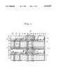
- FIG. 1shows structure 2 according to the present invention having two subcomponent assemblies 4 and 6.
- Structure 2can have any number of subcomponent assemblies.
- Each subcomponent assemblyis formed from a substrate 8 having a surface 10 which has a multilevel wiring structure 12 formed thereon.
- Multilevel wiring structure 12is formed from a dielectric material, such as an oxide, a glass, a polymer and a ceramic, most preferably a polyimide polymer.
- Multilevel wiring structure 12contains at least one layer of electrical conductors 14, such as copper, aluminum and gold, and has on surface 16 a plurality of contact locations 18.
- Substrate 8is shown in FIG. 1 as having vias 20 extending from surface 10 to surface 22.
- Surface 22has a multilayer wiring structure 24 which is similar to multilayer wiring structure 12.
- Surface 26 of multilayer wiring structure 24contains at least one electrically conductive layer 28 which is preferably copper, the dielectric material being preferably polyimide.
- Surface 26has a plurality of electrical contact locations 30 which are preferably copper coated with gold.
- Electrical contact layers 18are also preferably copper with a top coating of gold.
- Substrate 8can be any commonly used multilayered packaging substrate containing a plurality of electrical conductors or glass ceramic and is preferably a highly thermally conductive material such as synthetic diamond, aluminum nitride ceramic, silicon a metal (such as copper) with an electrically insulating coating.
- Substrate 8preferably has electrically conductive studs or vias 20 or through holes with a sidewall plated with an electrical conductor, such as copper, palladium, platinum and gold, as is commonly known in the art.
- the electrical conductors in multilayer structures 12 on surface 10 of substrate 8are electrically interconnected to contact locations 32 which are connected to via or stud 20 in substrate 8.
- Electrical conductors 28 in multilayer structure 24 on surface 22 of substrate 8are electrically interconnected to contact locations 34 which are electrically interconnected to vias or studs 20 in substrate 8.
- Contact locations 32 and 34are preferably formed from copper having a top surface gold.
- a plurality of electronic devices 36 and 38are mounted onto surface 16 of multilayer wiring structure 12.
- Electronic device 36is mounted in a flip-chip-configuration onto surface 16 with solder mounds 40, commonly known as C4s, electrically interconnecting the electronic device 36 to the contact locations 18.
- solder mounds 40commonly known as C4s
- Electronic device 38is mounted with active face 42 facing upwards and its nonactive face 44 in contact with surface 16 of multilayer structure 12.
- device 38may be mounted directly with its nonactive face 44 in contact with surface 10 of substrate 8. This is accomplished by removing a section of multilayer structure 12.
- Wires 46commonly made of aluminum or gold are bonded between contact location 18 and contact location 47 on surface 42 of electronic device 38. Wires 46 are bonded by commonly known wire bonding techniques, ultrasonic bonding techniques, laser bonding techniques and the like.
- the electrical interconnection means 49has a top surface 48 having contact locations 50 and a bottom surface 52 having contact locations 54.
- Contact locations 54are in electrical interconnection with contact locations 18 between chips 36 and 38.
- Contact locations 50are in electrical interconnection with contact locations 30 on surface 26 of multilayer structure 24.
- FIG. 2shows a partial view of the structure of FIG. 1 in perspective with a region of the right forward most corner of each substrate 8 partially cut away to reveal vias or studs 20.
- contact locations 18 and electrical conductors 60which electrically interconnect some of the contact locations 18.
- the electrical interconnection means 49is shown only partially as a plurality of electrical conductors 62 and 64. The electrical interconnection means will be described in greater detail hereinbelow.
- FIG. 3shows a top view of one of the subcomponent assemblies 4 or 6 of FIG. 1 showing the electrical interconnection means 49 having a plurality of apertures 66.
- the apertures 66are adapted to receive a plurality of electronic devices 68 which are disposed on surface 16 of multilevel wiring structure 12 of FIG. 1. Numbers common between FIGS. 1, 2 and 3 represent the same thing.
- FIG. 4shows a perspective view of the structure shown in FIG. 1 plus heat dissipation means 51 and 53. Numbers common between FIGS. 1, 2, 3 and 4 represent the same thing.
- Heat dissipation means 51 and 53are in thermal contact with substrates 8.
- the heat dissipation meansis preferably made of aluminum.
- Substrate 8is held in grooves in heat dissipation means 51 and 53 to ensure good thermal contact, mechanical support and compresses the interconnection means 49 between adjacent assemblies to provide electrical interconnection therebetween as described herein below.
- Heat dissipation means 51 and 53are held in a support frame (not shown).
- the thin film wiring layers 12 and 14 of FIG. 1preferably contain at least one plain pair (XY) of wiring and two reference planes which provide power and ground to the electronic devices 36 and 38. If the electronic devices are bipolar chips there are preferably two additional power planes.
- the dimensions of the wiring and the thickness of the reference planesdepends on the specific application and it can vary from 8 micron wide lines, 5 micron thick, on a 25 micron pitch to 25 micron wide lines, 25 microns thick on a pitch of 75 micron or more.
- the thickness of the insulation in the thin film wiring layers 12 and 24is adjusted to provide the required transmission line impedance that is typically in the range of 4 to 80 ohms.
- the electrical interconnection means 49is formed to occupy the space between the chips as shown in FIGS. 1-4.
- the structure of FIG. 1is compressed from the top and bottom of the structure to compress the electrical interconnection means 46 between the adjacent assemblies pressing electrical contact locations 30 on substrate 8 in contact with electrical contact locations 50 on electrical interconnection means 49 and pressing electrical contact locations 54 on electrical interconnection means 49 in contact with electrical contact locations 18 on the surface of the thin film wiring layer 12.
- a signal from any one chipwill travel in the thin film wiring layer and vertically through the electrical interconnection wiring means 49 to any thin film wiring plane in the stack of substrates 8 and thus along the shortest path to any chip in the entire structure 2. If a single plane contained 25 chips, for example, as shown in FIG.
- the electrical interconnection means 46would occupy the 1 centimeter space between each chip.
- the vias in the substrates 8 and the connections in the electrical interconnection means 49could be made on a 36 mil square grid with 20 mil wide pads 18 on the substrate 8. There would be approximately 6,694 vertical signal connections possible on one plane. The grid could be reduced by a factor of approximately 2 if required and 26,000 vertical connections could be made.
- the overall high performance packagecan consist of as many insulating plates populated by chips as required.
- the heatwould be conducted to the edges of the high thermal conductivity substrates 8 where it would be carried away by air or water cooled or the like heat sinks as appropriate and commonly known in the art.
- the substratesare preferably made of a high thermally conductive insulating material made of commercial diamond (manufactured For example by NORTON Inc. and Diamonex Inc.) which can be laser drilled to form vias and metallized for through hole connections using standard processing such as the process used on diamond heat spreaders for diode lasers.
- the very high thermal conductivity of diamond(1500 W/m°K.) makes it the most desirable material in this structure and would allow the cooling of more than 100 watts per plane. Other materials are useful.
- a lower cost alternativewould be AnN ceramic with co-sintered solid vias, which are commercially available or silicon wafers which can contain laser drilled holes or chemically etched through vias.
- the thin film wiring layer 12 and 24preferably contains copper wiring in a polyimide dielectric and can be fabricated by standard sequential thin film processes directly onto substrate 8 as described in R. Tummala and E. Rymasizewski, Microelectronics Packaging Handbook, Van Nostrand, Rienhold, N.Y., 1989 Chapter 9, the teaching of which is incorporated herein by reference.
- the thin film wiring structurecan be fabricated separately by the serial/parallel thin film wiring process and joined to the substrates 8 as described in U.S. patent application Ser. No. 07/695,368, filed May 3, 1991, now U.S. Pat. No. 5,258,236 the teaching of which is incorporated herein by reference.
- the electrical interconnection means 49preferably contains gold wires held at a slight angle in an elastomeric matrix. Other embodiments of large area array connectors can also work.
- the electrical interconnection means 49 using an elastomeric matrixhas desirable properties such as lower resistance, low contact force, wipe, and low inductance which makes it particularly desirable in this application.
- the electrical interconnection means 49can be fabricated to be approximately 1 millimeter thick with 10 percent compliance.
- the substrates 8are made with conducting vias. Top and bottom surface pads are applied by standard techniques such as evaporation of metals through a metal mask as described in Tiemmala et al., chapter 9 above.
- the electronic devices 36 and 38are joined to each thin film wiring layer after the electronic devices are tested and burned in.
- the electrical interconnection means 49are fabricated separately and tested. Finally, the stack of assemblies with electronic devices mounted onto the substrates with the electrical interconnection means 49 disposed thereon are aligned and a compressive force is applied to make the interconnections. The force is preferably from 10 to 50 grams per contact or from 70 to 300 kilograms for the entire package. The connection is separable.
- FIGS. 5-21show the method for fabricating electrical interconnection means 49 of FIG. 1 and show various embodiments and fabrication techniques of this electrical interconnection means.
- FIG. 5shows electrical interconnection means 80 which corresponds to electrical interconnection means 49 of FIG. 1.
- the electrical interconnection means 80is formed from an elastomeric material 82 having a plurality of electrical conductors 84 extending from side 86 to side 88 thereof.
- Each conductor 84preferably has a generally spherical end 90 at side 86 and a flattened spherical shape 92 at side 88.
- the conductors 84are preferably gold, gold alloy or copper alloy.
- the size, shape and the spacing of wires 84 along with the material properties of the elastomeric material 82can be modified to optimize the connector for a specific application.
- FIG. 6shows substrate 94 and 96 pressed towards each other as indicated by arrows 98 and 100 with interposer 80 therebetween.
- the elastomer 82acts as a spring to push the enlarged end contact surfaces 90 and 92 against mating contacts 104 and 106 on substrates 94 and 96 respectively.
- Surface 102 of substrate 94has contact locations 104 which are typically metalized pad.
- Substrate 96has contact locations 106 which are also typically metallized pads.
- This lateral movementresults in a wiping action which breaks a surface oxide which is on the surface of the contact locations 104 and 106 and which is on the surface of the enlarged ends 90 and 92.
- the wiping actionmakes a good electrical contact between the enlarged surface 90 and 92 and the contact locations 104 and 106, respectively.
- the advantages and unique features of the electrical interconnection means 80are that it provides uniform spacing of the electrical conductors 84 and the elastomer material on, for example, a 0.008 inch minimum pitch using a single wire per contact.
- the enlarged ball shaped contacts 90protrude from top side 86 of interconnection means 80 and the enlarged, flattened contacts 92 are generally flush with the bottom surface 88 of interconnection means 80. Textured or raised contact surface can be formed on the bottom side of the contact 92 to enhance the contact interface to an electrical contact location on substrate 96.
- the wires 84 in the elastomer material 82can be grouped into small clusters to provide redundant connections for each contact location 104 or 106. If clustered wires are used, wires 95 in interconnect structure 80 of FIG. 6 would be eliminated.
- FIG. 7shows a cross section of another embodiment 110 corresponding to the electrical interconnection means 49 of FIG. 1.
- Structure 110has electrical conductors 112 which are clustered into groups 114. Between each group there are grooves 116.
- the elastomer material 118is preferably a silicone elastomer and there are ball shaped contacts 120 on side 122 and flat contact 124 on side 126 having a raised surface 128.
- the top and bottom wire shapescan be varied for optimization.
- the alignment grooves 116 of structure 110can be formed using a laser, electron beam or other sensing techniques as described in U.S. Pat. No. 4,998,885, to Beaman, the teaching of which is incorporated herein by reference.
- Alignment features 116can be molded into the elastomer material to allow accurate alignment of the conductors 112 in the structure 110 with contact locations 104 and 106 on surfaces 102 and 105, respectively, as shown in FIG. 6.
- An alignment mechanismis preferred to enhance accurate positioning of the interposer wires with the contacts on the adjacent substrates.
- the molded alignment featurescan also be used to control the shrinkage and distortion of the contact grid in the elastomer material. Mechanically or thermally induced stress in the elastomer material can cause the interposer to distort causing alignment problems with the mating contacts.
- the electrical interconnection means shown in FIGS. 5, 7 and 8 and electrical interconnection means 49 of FIG. 1will also be referred to herein as an ELASTICON interposer.
- the ELASTICON interposeris designed to provide signal and power connections from the bottom surface of a substrate to another substrate.
- the ELASTICON interposercan be fabricated to have a full array of conductors or a clustered array of conductors.
- the interposer connector that uses a full array of conductors (or wires)would typically not require alignment of the connector to the contact locations on the substrates between which is disposed. By using clusters of wires, overall fewer wires are used to fabricate the interposer. This is useful for reducing the cost of the connector and the pressure required to ensure full engagement of the contacts.
- Interposer contacts that use a clustered array of wirespreferably have a means for aligning the wire clusters with the remaining said contacts.
- An interposer having a cluster set of wiresminimizes the number of wires required during the interposer fabrication and enhances the compliance of the connector assembly.
- the molded or scribed grooves or other features in the elastomer materialcan be used to allow the interposer connector to self align with similar features on the substrates between which it is disposed as shown in FIG. 8.
- FIG. 8shows interpfser 119 disposed on substrate 121.
- Interposer 119has grooves 123 which mate with projections 125 on substrate 121 which aligns substrate pads 127 to interposer contact locations 129.
- FIG. 10shows a perspective view of an ELASTICON interposer useful as the electrical interconnection means 49 of FIG. 1.
- the ELASTICON interposer 134 of FIG. 10has a plurality of alignment grooves 136 and regions 138 containing clustered contacts wherein each region is surrounded by grooves 140.
- FIG. 9shows an alignment frame 142 which is adapted for engagement with the grooves on the interposer 134 of FIG. 10 to align substrate contact locations to interposer contact locations.
- bar 144 in alignment frame 142engages groove 146 of structure 134 of FIG. 10
- bar 148 of frame 142engages groove 150 of structure 134 of FIG. 10.
- the frameis disposed on a substrate having contact locations to which interposer contact locations are to be aligned.
- Each of the disconnectable elements of the modulepreferably have a means of alignment to the other elements in the module.
- a separate alignment framecould be attached to each substrate similar to the one used for the interposer.
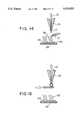
- FIGS. 11-19show a fabrication method for the ELASTICON interposers described herein.
- the fabrication processstarts with a sacrificial substrate 160, which is preferably copper, copper/Invar/copper or copper/molybdenium copper. Materials other than copper can be used such as aluminum, hard plastic or steel.
- the substrate 160can be fabricated to have protuberances 162 which provide the grooves 116 in the ELASTICON interposers of FIG. 7.
- the protuberances 162can be formed using various fabrication techniques including machining of the surface 164 or stamping of the surface 164.
- the top surface 164is sputtered or plated with soft gold or Ni/Au to provide a suitable surface for thermosonic ball bonding.
- a commonly used automatic wire bonderis modified to ball bond gold, gold alloy, copper, copper alloy, aluminum, nickel or palladium wires 166 to the subtrate surface 164 as shown in FIG. 11.
- the wirepreferably has a diameter of 0.001 to 0.005 inches.
- a thin passivation metalsuch as Au, Cr, Co, Ni or Pd can be coated over the wire by means of electroplating, or electroless plating, sputtering, e-beam evaporation or any other coating techniques known in the industry.
- Structure 168 of FIG. 11is the ball bonding head which has a wire 170 being fed from a reservoir of wire as in a conventional wire bonding apparatus.
- FIG. 11shows the ball bond head 168 in contact at location 169 with surface 164 of substrate 160.
- FIG. 12shows the ball bonding head 168 withdrawn in the direction indicated by arrow 171 from the surface 164 and the wire 170 drawn out to leave disposed on the surface 164 wire 166.
- the bond head 168is stationary and the substrate 160 is advanced as indicated by arrow 161.
- the bond wireis positioned at an angle preferably between 5° to 60° from vertical and then mechanically severed by knife edge 172 as shown in FIG. 13.
- the knife edge 172is actuated, the wire 170 is clamped and the bond head 168 is raised.
- a flying lead 166which is bonded to surface 164 at one end and the other end projects outwardly away from the surface.
- a ballcan be Formed on the end of the wire 166 which is not bonded to surface 164 using a laser or electrical discharge to melt the end of the wire. Techniques for this are commonly known in the art.
- a split beam laser delivery systemsdescribed hereinbelow, is used to localize the laser energy to a single wire for forming the ball. This minimizes the laser energy absorbed by adjacent wires that could cause the wires to deform.
- a ballis not required on the end of the wire. This modified wire bonding process is repeated to form a dense array of angled wires on the substrate.
- FIG. 14shows the wire 170 severed to leave wire 166 disposed on surface 164 of substrate 160.
- the wire bond head 168is retracted upwardly as indicated by arrow 174.
- the wire bond head 168has a mechanism to grip and release wire 170 so that wire 170 can be tensioned against the shear blade to sever the wire.
- FIG. 15shows that after the wire is severed, the bond head is raised to a "home" position.
- An electronic flame off unit(part of Hughes Wire Bonder, Modec III-2640) electrode is positioned below the bond head and an electrical discharge from the electrode is used to melt the wire in the capillary tip to form a ball.
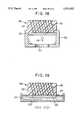
- the substrate 160is placed in a casting mold 190 as shown in FIG. 16.
- a controlled volume of liquid elastomer 192is disposed into the casting mold and allowed to settle out (flow between the wires until the surface is level) before curing as shown in FIG. 17.
- the substrateis extracted from the mold as shown in FIG. 18 and indicated by arrow 194.
- the cured elastomeris represented by reference rule 196.
- Opening 161 in mold 190is a tooling feature for extracting the substrate from the mold.
- the structure 198is removed from the mold 190 and is placed in a sulfuric and nitric acid bath 200, as shown in FIG. 19 to dissolve the copper substrate 160.
- Ultrasonic agitation of the sulfuric and nitric acidhelps to facilitate the etching of the copper substrate and causes the gold plating on the surface of the copper substrate to flake off from the surface 202 of the elastomer material 196 leaving the surface of the ball bonds 204 exposed.
- the substratecan be made of peel-apart-copper, where a thin layer of copper is attached to a solid substrate with a marginal adhesion strength.
- the connectorcan be peeled off from the sacrificial substrate before the remaining thin copper is flash etched away.
- a high compliance, high thermal stability siloxane elastomer materialis preferable for this application.
- the high temperature siloxane materialis cast or injected and cured similar to other elastomeric materials.
- the elastomeris preferably cured at lower temperature (T ⁇ 60°) followed by complete cure at higher temperatures (T ⁇ 80°).
- the connectoris cast into a plastic frame, which was predrilled with holes around its periphery. When the elastomer is poured into this frame a physical locking of the elastomer to the frame takes place which both holds the elastomer/connector to the frame and minimizes the shrinkage.
- a foam agentcan be blended into the commercial elastomeric material at a ratio ranging from 10 to 60%. Also, foam can be employed as a distinct layer.
- the use of polydimethylsiloxane based rubbersbest satisfy both the material and processing requirements.
- the thermal stability of such elastomersis limited at temperatures below 200° C. and significant outgassing is observed above 100° C.
- the thermal stabilitycan be significantly enhanced by the incorporation of 25 wt % or more diphenylsiloxane (FIG. 1).
- enhancement in the thermal stabilityhas been demonstrated by increasing the molecular weight of the resins (oligomers) or minimizing the crosslink junction. The outgassing of the elastomers can be minimized at temperatures below 300° C.
- FIG. 11when bond head 168 bonds the wire 170 to the surface 164 of substrate 160 there is formed a flattened spherical end shown as 204 in FIG. 19.
- the protuberances 162 on substrate 160 as shown in FIG. 11result in grooves in the elastomer such as grooves 116 shown in FIG. 7. These grooves form alignment features.
- the design and tolerances used to form the copper substrate 160are preferably carefully matched with the design and tolerances used to fabricate the alignment features on the substrates 94 and 96 shown in FIG. 6.
- an alignment framesuch as shown in FIG. 9, can be disposed on the surface of a substrate, such as 94 and 96, of FIG. 6 and the elasticon interposer with grooves can be disposed onto this alignment frame so that the alignment grooves of the interposei engage the frame pattern as describe herein above with respect to FIGS. 9 and 10.
- multiple substrates 210 each having a group of wires 212 disposed thereoncan be placed into a common mold 214 into which the liquid elastomer 216 as described herein above is disposed and cured.
- the cured elastomerlinks the substrates together into a single interposer 218 as shown in FIG. 21.
- Grooves 211are for compliance or alignment requirements.
- several smaller connectorscan be fabricated on the same substrate as a single unit and then separated after the elastomer is cured and the substrate is etched away.
- the surface of the copper sacrificial substratecan be textured or embossed prior to gold plating and wire bonding to provide a textured or raised contact surface on the bottom of the ball bonds.
- the completed interposer 218 of FIG. 21can be further modified by using a laser to scribe channels in the elastomeric material between the bond wires at an angle matching the angle of the bond wires, as shown in FIG. 7.
- the criss-crossing channelscreate independent elastomeric columns (shown in FIG. 10 as 138) surrounding the gold wires. This would allow individual wires or groups of wires to compress independently and allow the interposer to compensate for slight variations in the remaining surfaces while reducing the total pressure required to compress the entire interposer.
- Patterned connectorscan easily be fabricated by programming the wire bonder to a specific pattern and molding the elastomer to provide holes or open areas in the connector that correspond with other electronic or mechanical components surrounding the connector.
- groovesare preferably molded into the elastomer on both sides of the connector surfaces in both the X and Y directions or in a circular geometry.
- the width and depth of the grooveare preferably wider than 5 mils and deeper than 10 mils, respectively, in an interposer 100 mils thick.
- the groovesare preferably molded in a direction parallel to the angled wire.
- Grooveshave been fabricated with laser, electron beam, metal mask and slicing with a blade. Other techniques such as stamping, injection molding and other known techniques to create the desired geometry would also work well.
- the contact balls at the end of the wiresare formed using a split beam laser configuration.
- the end of each wirewill melt and form the ball only at the point where the two beams intersect.
- FIG. 22which shows light source 300, preferably an argon-ion laser which is the source of light beam 302 which is reflected as light beam 304 by mirror 306.
- Light beam 304is directed through light beam expander 308 to form expanded light beam 310.
- Expanded light beam 310is directed to beam splitter 312 which splits beam 310 into beams 314 and 316.
- Beam 316is reflected off mirror 322 as light beam 324.
- Beam 314is reflected off mirror 318 as light beam 320.
- Beam 320is passed through focusing lens 328 to form focused beams 330 which focused onto spot 332 on the workpiece which is the end of a wire.
- Beam 324is passed through focussing lens 334 to form focused beam 336 which is focussed onto spot 332 on the workpiece.
- the workpieceis disposed on x-y table 338. The beam is expanded before Focussing to get the desired size of spot 332.
- FIG. 23shows an enlarged view of the region of FIG. 7 enclosed in the dashed circle 230.
- Element 124is a flattened ball shape member at the end of conductor 112.
- the flattened ball shaped member 124was formed when conductor 112 was wire bonded to the sacrificial copper layer as described with reference to FIG. 11.
- the sacrificial copper layercan be fabricated with an array of pits in the surface in the regions where the wires 112 are bonded. These pits can have, for example, a hemispherical shape, rectangular shape, pyrimidal shape or any other shape. If such an array of pits are used and the wire is bonded in the region of the pit, a protuberance such as 128 of FIG. 22 is formed at the surface 232 of flattened ball. This protuberance provides a projecting region to the contact formed by flattened ball 124 which can wipe on the surface of the contact location to which the flattened ball is to be electrically connected.
Landscapes
- Physics & Mathematics (AREA)
- General Physics & Mathematics (AREA)
- Engineering & Computer Science (AREA)
- Microelectronics & Electronic Packaging (AREA)
- Computer Hardware Design (AREA)
- Power Engineering (AREA)
- Condensed Matter Physics & Semiconductors (AREA)
- General Engineering & Computer Science (AREA)
- Measuring Leads Or Probes (AREA)
- Testing Or Measuring Of Semiconductors Or The Like (AREA)
- Manufacturing Of Electrical Connectors (AREA)
- Cooling Or The Like Of Semiconductors Or Solid State Devices (AREA)
- Multi-Conductor Connections (AREA)
Abstract
Description
This is a division of application Ser. No. 07/963,346, filed Oct. 19, 1992, U.S. Pat. No. 5,371,654.
The present invention is directed to packaging structures for interconnecting electronic devices in a three dimensional structure. More particularly, the present invention is directed to a structure having a plurality of substrates wherein each substrate has a plurality of electronic devices thereon forming an assembly. There are a plurality of assemblies disposed one on top of each other with a vertical wiring interconnection structure disposed between adjacent assemblies. Most particularly, the vertical wire interconnection structure contains a plurality of electrical conductors disposed in an elasomteric material and is compressed between adjacent assemblies.
In the microelectronics industry, integrated circuits, such as semiconductor chips, are mounted onto packaging substrates to form modules. In high performance computer applications, these modules contain a plurality of integrated circuits. A plurality of modules are mounted onto a second level of packages such as a printed circuit board or card. The cards arc inserted in a frame to form a computer.
In nearly all conventional interconnection packages except for double sided cards, signals from one chip on the package travel in a two dimensional wiring net to the edge of the package then travel across a card or a board or even travel along cables before they reach the next package containing the destination integrated circuit chip. Therefore, signals must travel off of one module onto wiring on a board or onto wiring on a cable to a second module and from the second module to the destination integrated circuit chip fn the module. This results in long package time delays and increases the wireability requirement of the two dimensional wiring arrays.
An improvement in interchip propagation time and increase in real chip packaging density can be achieved if three dimensional wiring between closely spaced planes of chips could be achieved.
U.S. patent application Ser. No. 5,099,309 describes a three dimensional semiconductor chip packaging structure which comprises a plurality of stacked cards. Each card is specially fabricated to have cavities on both sides thereof which contain chips. On each surface of the card, there are electrical conductors which are bonded by wires to contact locations on the chips. Electrical conductors extend through the cards between the chip containing regions and to contact locations on each side of the card. These contact locations have dendrites on the surface. The cards are stacked so that the dendrite covered contact locations on adjacent sides of adjacent cards intermesh to provide electrical interconnection between the adjacent cards. This structure requires a high degree board flatness for the connections to be mated.
It is an object of the present invention to provide improved three dimensional integrated circuit packaging structures.
Another object of the present invention is to provide such a packaging structures with both horizontal electrical interconnections and compliant vertical electrical interconnections.
A further object of the present invention is to provide such structures which can be assembled and disassembled into a plurality of subassemblies.
An additional object of the present invention is to provide such structures which have a high thermal dissipation capacity.
Yet another object of the present invention is to provide such structures which does not require rigid electrical interconnection between subassemblies.
Yet a further object of the present invention is to provide such structures which can be fabricated using conventional packaging substrates.
A broad aspect of the present invention is a structure having a plurality of assemblies. Each of the assemblies is formed from a substrate having a first and second opposing surfaces. There are a plurality of electronic devices disposed on at least one of the first and second surface of the substrate of each assembly. Each of the plurality of assemblies is disposed adjacent another of the plurality of assemblies so that the first surface of one of the adjacent assemblies is adjacent the second surface of the other of the adjacent assemblies. An electrical interconnection means is disposed between the first and second surfaces of the adjacent assemblies and provides electrical interconnection between contact locations on the adjacent surfaces. The electrical interconnection means is formed from a dielectric material having first and second opposing surfaces and a plurality of electrical contact locations on each surface which are electrically interconnected by a plurality of electrical conductors extending from the first surface to the second surface of the electrical interconnection means.
In a more particular aspect of the present invention, the substrates of the assemblies are formed from a diamond like material which has high thermal dissipation capacity.
In another more particular aspect of the present invention, the substrates have a plurality of dielectric and electrically conducting layers.
In another more particular aspect of the present invention, a heat dissipation means dissipates heat generated in the structure.
These and other objects, features and advantages of the present invention will become apparent upon further consideration of the following detailed description of the invention when read in conjunction with the figures, in which:
FIG. 1 shows a side view of a three dimensional electronic device packaging structure according to the present invention.
FIG. 2 shows a partial perspective view of the structure of FIG. 1.
FIG. 3 shows a top view of the electrical interconnection means of the structure of FIG. 1.
FIG. 4 shows a perspective view of the structures of FIG. 1 including a heat dissipation means.
FIG. 5 shows a cross sectional view of a section of the electrical interconnection means of the structure of FIG. 1.
FIG. 6 shows the structure of FIG. 5 disposed under pressure between two adjacent substrates.
FIG. 7 shows another embodiment of the structuie of FIG. 5 having grooves on the two opposing surfaces.
FIG. 8 shows grooves on an interposer engaging projections on a substrate to align substrate and interposer contact locations.
FIG. 9 shows an alignment frame for mating with alignment grooves such as shown in the structure of FIG. 10.
FIG. 10 shows an interconnection structure having grooves for mating with the frame of FIG. 9.
FIGS. 11-19 show the process for making the electrical interconnection means, for example, of FIG. 5.
FIGS. 20 and 21 show an alternate embodiment of some of the method steps for fabricating an electrical interconnection means.
FIG. 22 schematically shows an optical system to form balls on the end of the wire conductors in FIG. 15.
FIG. 23 is an enlarged view of the region of FIG. 7 enclosed indashed circle 230.
FIG. 1 showsstructure 2 according to the present invention having twosubcomponent assemblies Structure 2 can have any number of subcomponent assemblies. Each subcomponent assembly is formed from asubstrate 8 having asurface 10 which has amultilevel wiring structure 12 formed thereon.Multilevel wiring structure 12 is formed from a dielectric material, such as an oxide, a glass, a polymer and a ceramic, most preferably a polyimide polymer.Multilevel wiring structure 12 contains at least one layer ofelectrical conductors 14, such as copper, aluminum and gold, and has on surface 16 a plurality ofcontact locations 18.Substrate 8 is shown in FIG. 1 as havingvias 20 extending fromsurface 10 tosurface 22.Surface 22 has amultilayer wiring structure 24 which is similar tomultilayer wiring structure 12.Surface 26 ofmultilayer wiring structure 24 contains at least one electricallyconductive layer 28 which is preferably copper, the dielectric material being preferably polyimide.Surface 26 has a plurality ofelectrical contact locations 30 which are preferably copper coated with gold. Electrical contact layers 18 are also preferably copper with a top coating of gold.
The electrical conductors inmultilayer structures 12 onsurface 10 ofsubstrate 8 are electrically interconnected to contact locations 32 which are connected to via orstud 20 insubstrate 8.Electrical conductors 28 inmultilayer structure 24 onsurface 22 ofsubstrate 8 are electrically interconnected to contactlocations 34 which are electrically interconnected to vias orstuds 20 insubstrate 8. Contactlocations 32 and 34 are preferably formed from copper having a top surface gold.
A plurality ofelectronic devices surface 16 ofmultilayer wiring structure 12.
Disposed betweenelectronic devices
The electrical interconnection means 49 has atop surface 48 havingcontact locations 50 and abottom surface 52 havingcontact locations 54. Contactlocations 54 are in electrical interconnection withcontact locations 18 betweenchips locations 50 are in electrical interconnection withcontact locations 30 onsurface 26 ofmultilayer structure 24.
FIG. 2 shows a partial view of the structure of FIG. 1 in perspective with a region of the right forward most corner of eachsubstrate 8 partially cut away to reveal vias orstuds 20. Onsurface 16, there is seencontact locations 18 andelectrical conductors 60 which electrically interconnect some of thecontact locations 18. The electrical interconnection means 49 is shown only partially as a plurality ofelectrical conductors
FIG. 3 shows a top view of one of thesubcomponent assemblies apertures 66. Theapertures 66 are adapted to receive a plurality ofelectronic devices 68 which are disposed onsurface 16 ofmultilevel wiring structure 12 of FIG. 1. Numbers common between FIGS. 1, 2 and 3 represent the same thing.
FIG. 4 shows a perspective view of the structure shown in FIG. 1 plus heat dissipation means 51 and 53. Numbers common between FIGS. 1, 2, 3 and 4 represent the same thing. Heat dissipation means 51 and 53 are in thermal contact withsubstrates 8. The heat dissipation means is preferably made of aluminum.Substrate 8 is held in grooves in heat dissipation means 51 and 53 to ensure good thermal contact, mechanical support and compresses the interconnection means 49 between adjacent assemblies to provide electrical interconnection therebetween as described herein below. Heat dissipation means 51 and 53 are held in a support frame (not shown).
The thin film wiring layers 12 and 14 of FIG. 1 preferably contain at least one plain pair (XY) of wiring and two reference planes which provide power and ground to theelectronic devices
The electrical interconnection means 49 is formed to occupy the space between the chips as shown in FIGS. 1-4. The structure of FIG. 1 is compressed from the top and bottom of the structure to compress the electrical interconnection means 46 between the adjacent assemblies pressingelectrical contact locations 30 onsubstrate 8 in contact withelectrical contact locations 50 on electrical interconnection means 49 and pressingelectrical contact locations 54 on electrical interconnection means 49 in contact withelectrical contact locations 18 on the surface of the thinfilm wiring layer 12. Thus, a signal from any one chip will travel in the thin film wiring layer and vertically through the electrical interconnection wiring means 49 to any thin film wiring plane in the stack ofsubstrates 8 and thus along the shortest path to any chip in theentire structure 2. If a single plane contained 25 chips, for example, as shown in FIG. 3, each being 1 centimeter square, then the electrical interconnection means 46 would occupy the 1 centimeter space between each chip. With this design point the vias in thesubstrates 8 and the connections in the electrical interconnection means 49 could be made on a 36 mil square grid with 20 milwide pads 18 on thesubstrate 8. There would be approximately 6,694 vertical signal connections possible on one plane. The grid could be reduced by a factor of approximately 2 if required and 26,000 vertical connections could be made.
The overall high performance package can consist of as many insulating plates populated by chips as required. The heat would be conducted to the edges of the highthermal conductivity substrates 8 where it would be carried away by air or water cooled or the like heat sinks as appropriate and commonly known in the art.
The substrates are preferably made of a high thermally conductive insulating material made of commercial diamond (manufactured For example by NORTON Inc. and Diamonex Inc.) which can be laser drilled to form vias and metallized for through hole connections using standard processing such as the process used on diamond heat spreaders for diode lasers. The very high thermal conductivity of diamond (1500 W/m°K.) makes it the most desirable material in this structure and would allow the cooling of more than 100 watts per plane. Other materials are useful. A lower cost alternative would be AnN ceramic with co-sintered solid vias, which are commercially available or silicon wafers which can contain laser drilled holes or chemically etched through vias. The thinfilm wiring layer substrate 8 as described in R. Tummala and E. Rymasizewski, Microelectronics Packaging Handbook, Van Nostrand, Rienhold, N.Y., 1989 Chapter 9, the teaching of which is incorporated herein by reference. The thin film wiring structure can be fabricated separately by the serial/parallel thin film wiring process and joined to thesubstrates 8 as described in U.S. patent application Ser. No. 07/695,368, filed May 3, 1991, now U.S. Pat. No. 5,258,236 the teaching of which is incorporated herein by reference. In the serial/parallel processes the thin film wiring structures are fabricated on separate carriers then transferred and laminated to the insulated plates preferably by thermal compression bonding. The electrical interconnection means 49 preferably contains gold wires held at a slight angle in an elastomeric matrix. Other embodiments of large area array connectors can also work. The electrical interconnection means 49 using an elastomeric matrix has desirable properties such as lower resistance, low contact force, wipe, and low inductance which makes it particularly desirable in this application. The electrical interconnection means 49 can be fabricated to be approximately 1 millimeter thick with 10 percent compliance.
Thesubstrates 8 are made with conducting vias. Top and bottom surface pads are applied by standard techniques such as evaporation of metals through a metal mask as described in Tiemmala et al., chapter 9 above. Theelectronic devices
FIGS. 5-21 show the method for fabricating electrical interconnection means 49 of FIG. 1 and show various embodiments and fabrication techniques of this electrical interconnection means.
FIG. 5 shows electrical interconnection means 80 which corresponds to electrical interconnection means 49 of FIG. 1. The electrical interconnection means 80 is formed from anelastomeric material 82 having a plurality ofelectrical conductors 84 extending fromside 86 toside 88 thereof. Eachconductor 84 preferably has a generallyspherical end 90 atside 86 and a flattenedspherical shape 92 atside 88. Theconductors 84 are preferably gold, gold alloy or copper alloy. The size, shape and the spacing ofwires 84 along with the material properties of theelastomeric material 82 can be modified to optimize the connector for a specific application.
FIG. 6 showssubstrate arrows interposer 80 therebetween. Theelastomer 82 acts as a spring to push the enlarged end contact surfaces 90 and 92 againstmating contacts substrates Surface 102 ofsubstrate 94 hascontact locations 104 which are typically metalized pad.Substrate 96 hascontact locations 106 which are also typically metallized pads. Whensubstrate 94 is pressed towardssubstrate 96 theends conductors 84 are at a nonorthogonal angle with respect thereto. This lateral movement results in a wiping action which breaks a surface oxide which is on the surface of thecontact locations enlarged surface contact locations
The advantages and unique features of the electrical interconnection means 80 are that it provides uniform spacing of theelectrical conductors 84 and the elastomer material on, for example, a 0.008 inch minimum pitch using a single wire per contact. The enlarged ball shapedcontacts 90 protrude fromtop side 86 of interconnection means 80 and the enlarged, flattenedcontacts 92 are generally flush with thebottom surface 88 of interconnection means 80. Textured or raised contact surface can be formed on the bottom side of thecontact 92 to enhance the contact interface to an electrical contact location onsubstrate 96. Thewires 84 in theelastomer material 82 can be grouped into small clusters to provide redundant connections for eachcontact location wires 95 ininterconnect structure 80 of FIG. 6 would be eliminated.
FIG. 7 shows a cross section of another embodiment 110 corresponding to the electrical interconnection means 49 of FIG. 1. Structure 110 haselectrical conductors 112 which are clustered intogroups 114. Between each group there aregrooves 116. Theelastomer material 118 is preferably a silicone elastomer and there are ball shapedcontacts 120 onside 122 andflat contact 124 onside 126 having a raisedsurface 128. The top and bottom wire shapes can be varied for optimization. Thealignment grooves 116 of structure 110 can be formed using a laser, electron beam or other sensing techniques as described in U.S. Pat. No. 4,998,885, to Beaman, the teaching of which is incorporated herein by reference.
Alignment features 116 can be molded into the elastomer material to allow accurate alignment of theconductors 112 in the structure 110 withcontact locations surfaces
The electrical interconnection means shown in FIGS. 5, 7 and 8 and electrical interconnection means 49 of FIG. 1 will also be referred to herein as an ELASTICON interposer. The ELASTICON interposer is designed to provide signal and power connections from the bottom surface of a substrate to another substrate. The ELASTICON interposer can be fabricated to have a full array of conductors or a clustered array of conductors. The interposer connector that uses a full array of conductors (or wires) would typically not require alignment of the connector to the contact locations on the substrates between which is disposed. By using clusters of wires, overall fewer wires are used to fabricate the interposer. This is useful for reducing the cost of the connector and the pressure required to ensure full engagement of the contacts. Interposer contacts that use a clustered array of wires preferably have a means for aligning the wire clusters with the remaining said contacts. An interposer having a cluster set of wires minimizes the number of wires required during the interposer fabrication and enhances the compliance of the connector assembly. The molded or scribed grooves or other features in the elastomer material can be used to allow the interposer connector to self align with similar features on the substrates between which it is disposed as shown in FIG. 8. FIG. 8 shows interpfser 119 disposed onsubstrate 121.Interposer 119 hasgrooves 123 which mate withprojections 125 onsubstrate 121 which alignssubstrate pads 127 tointerposer contact locations 129. These alignment features can be designed using a variety of simple geometric shapes such as circular post, rectangular ridges, or a raised grid pattern. FIG. 10 shows a perspective view of an ELASTICON interposer useful as the electrical interconnection means 49 of FIG. 1. TheELASTICON interposer 134 of FIG. 10 has a plurality ofalignment grooves 136 andregions 138 containing clustered contacts wherein each region is surrounded bygrooves 140.
FIG. 9 shows analignment frame 142 which is adapted for engagement with the grooves on theinterposer 134 of FIG. 10 to align substrate contact locations to interposer contact locations. For example,bar 144 inalignment frame 142 engagesgroove 146 ofstructure 134 of FIG. 10 and bar 148 offrame 142 engagesgroove 150 ofstructure 134 of FIG. 10. The frame is disposed on a substrate having contact locations to which interposer contact locations are to be aligned.
An overall alignment scheme is preferred to fabricate the structure of FIG. 1. Each of the disconnectable elements of the module preferably have a means of alignment to the other elements in the module. A separate alignment frame could be attached to each substrate similar to the one used for the interposer.
FIGS. 11-19 show a fabrication method for the ELASTICON interposers described herein.
The fabrication process starts with asacrificial substrate 160, which is preferably copper, copper/Invar/copper or copper/molybdenium copper. Materials other than copper can be used such as aluminum, hard plastic or steel. Thesubstrate 160 can be fabricated to haveprotuberances 162 which provide thegrooves 116 in the ELASTICON interposers of FIG. 7. Theprotuberances 162 can be formed using various fabrication techniques including machining of thesurface 164 or stamping of thesurface 164. After the substrate has been formed with the protuberances, thetop surface 164 is sputtered or plated with soft gold or Ni/Au to provide a suitable surface for thermosonic ball bonding. Other bonding techniques can be used such as thermal compression bonding, ultrasonic bonding, laser bonding and the like. A commonly used automatic wire bonder is modified to ball bond gold, gold alloy, copper, copper alloy, aluminum, nickel orpalladium wires 166 to thesubtrate surface 164 as shown in FIG. 11. The wire preferably has a diameter of 0.001 to 0.005 inches. If a metal other than Au is used, a thin passivation metal such as Au, Cr, Co, Ni or Pd can be coated over the wire by means of electroplating, or electroless plating, sputtering, e-beam evaporation or any other coating techniques known in the industry.Structure 168 of FIG. 11 is the ball bonding head which has awire 170 being fed from a reservoir of wire as in a conventional wire bonding apparatus. FIG. 11 shows theball bond head 168 in contact atlocation 169 withsurface 164 ofsubstrate 160.
FIG. 12 shows theball bonding head 168 withdrawn in the direction indicated by arrow 171 from thesurface 164 and thewire 170 drawn out to leave disposed on thesurface 164wire 166. In the preferred embodiment, thebond head 168 is stationary and thesubstrate 160 is advanced as indicated byarrow 161. The bond wire is positioned at an angle preferably between 5° to 60° from vertical and then mechanically severed byknife edge 172 as shown in FIG. 13. Theknife edge 172 is actuated, thewire 170 is clamped and thebond head 168 is raised. When thewire 170 is severed there is left on thesurface 164 of substrate 160 a flyinglead 166 which is bonded to surface 164 at one end and the other end projects outwardly away from the surface. A ball can be Formed on the end of thewire 166 which is not bonded to surface 164 using a laser or electrical discharge to melt the end of the wire. Techniques for this are commonly known in the art. A split beam laser delivery systems, described hereinbelow, is used to localize the laser energy to a single wire for forming the ball. This minimizes the laser energy absorbed by adjacent wires that could cause the wires to deform. A ball is not required on the end of the wire. This modified wire bonding process is repeated to form a dense array of angled wires on the substrate.
FIG. 14 shows thewire 170 severed to leavewire 166 disposed onsurface 164 ofsubstrate 160. Thewire bond head 168 is retracted upwardly as indicated byarrow 174. Thewire bond head 168 has a mechanism to grip andrelease wire 170 so thatwire 170 can be tensioned against the shear blade to sever the wire.
FIG. 15 shows that after the wire is severed, the bond head is raised to a "home" position. An electronic flame off unit (part of Hughes Wire Bonder, Modec III-2640) electrode is positioned below the bond head and an electrical discharge from the electrode is used to melt the wire in the capillary tip to form a ball.
After the wire bonding process is completed, thesubstrate 160 is placed in a castingmold 190 as shown in FIG. 16. A controlled volume ofliquid elastomer 192 is disposed into the casting mold and allowed to settle out (flow between the wires until the surface is level) before curing as shown in FIG. 17. Once the elastomer has cured, the substrate is extracted from the mold as shown in FIG. 18 and indicated byarrow 194. The cured elastomer is represented byreference rule 196. Opening 161 inmold 190 is a tooling feature for extracting the substrate from the mold. Thestructure 198 is removed from themold 190 and is placed in a sulfuric andnitric acid bath 200, as shown in FIG. 19 to dissolve thecopper substrate 160. Ultrasonic agitation of the sulfuric and nitric acid helps to facilitate the etching of the copper substrate and causes the gold plating on the surface of the copper substrate to flake off from thesurface 202 of theelastomer material 196 leaving the surface of theball bonds 204 exposed.
Alternatively, the substrate can be made of peel-apart-copper, where a thin layer of copper is attached to a solid substrate with a marginal adhesion strength. After the fabrication is completed, the connector can be peeled off from the sacrificial substrate before the remaining thin copper is flash etched away.
A high compliance, high thermal stability siloxane elastomer material is preferable for this application. The high temperature siloxane material is cast or injected and cured similar to other elastomeric materials. To minimize the shrinkage, the elastomer is preferably cured at lower temperature (T≦60°) followed by complete cure at higher temperatures (T≧80°). To further control the shrinkage, the connector is cast into a plastic frame, which was predrilled with holes around its periphery. When the elastomer is poured into this frame a physical locking of the elastomer to the frame takes place which both holds the elastomer/connector to the frame and minimizes the shrinkage. To improve the compliance and reduce the dielectric constant of the elastomer material, a foam agent can be blended into the commercial elastomeric material at a ratio ranging from 10 to 60%. Also, foam can be employed as a distinct layer.
Among the many commercially avaliable elastomers, such as ECCOSIL and SYLGARD, the use of polydimethylsiloxane based rubbers best satisfy both the material and processing requirements. However, the thermal stability of such elastomers is limited at temperatures below 200° C. and significant outgassing is observed above 100° C. We have found that the thermal stability can be significantly enhanced by the incorporation of 25 wt % or more diphenylsiloxane (FIG. 1). Further, enhancement in the thermal stability has been demonstrated by increasing the molecular weight of the resins (oligomers) or minimizing the crosslink junction. The outgassing of the elastomers can be minimized at temperatures below 300° C. by first using a thermally transient catalyst in the resin synthesis and secondly subjecting the resin to a thin film distillation to remove low molecular weight side-products. For our experiments, we have found that 25 wt % diphenylsiloxane is optimal, balancing the desired thermal stability with the increased viscosity associated with diphenylsiloxane incorporation. The optimum number average molecular weight of the resin for maximum thermal stability was found to be between 18,000 and 35,000 g/mol. Higher molecular weights were difficult to cure and too viscous, once filled, to process. Network formation was achieved by a standard hydrosilylation polymerization using a hindered platinum catalyst in a reactive silicon oil carrier.
In FIG. 11 whenbond head 168 bonds thewire 170 to thesurface 164 ofsubstrate 160 there is formed a flattened spherical end shown as 204 in FIG. 19. Theprotuberances 162 onsubstrate 160 as shown in FIG. 11 result in grooves in the elastomer such asgrooves 116 shown in FIG. 7. These grooves form alignment features. The design and tolerances used to form thecopper substrate 160 are preferably carefully matched with the design and tolerances used to fabricate the alignment features on thesubstrates
Referring to FIG. 20,multiple substrates 210 each having a group ofwires 212 disposed thereon can be placed into acommon mold 214 into which theliquid elastomer 216 as described herein above is disposed and cured. The cured elastomer links the substrates together into asingle interposer 218 as shown in FIG. 21.Grooves 211 are for compliance or alignment requirements. Alternatively, several smaller connectors can be fabricated on the same substrate as a single unit and then separated after the elastomer is cured and the substrate is etched away.
Also, the surface of the copper sacrificial substrate can be textured or embossed prior to gold plating and wire bonding to provide a textured or raised contact surface on the bottom of the ball bonds. The completedinterposer 218 of FIG. 21 can be further modified by using a laser to scribe channels in the elastomeric material between the bond wires at an angle matching the angle of the bond wires, as shown in FIG. 7. The criss-crossing channels create independent elastomeric columns (shown in FIG. 10 as 138) surrounding the gold wires. This would allow individual wires or groups of wires to compress independently and allow the interposer to compensate for slight variations in the remaining surfaces while reducing the total pressure required to compress the entire interposer. Patterned connectors can easily be fabricated by programming the wire bonder to a specific pattern and molding the elastomer to provide holes or open areas in the connector that correspond with other electronic or mechanical components surrounding the connector.
To improve compliance and reduce wire deformation, grooves are preferably molded into the elastomer on both sides of the connector surfaces in both the X and Y directions or in a circular geometry. The width and depth of the groove are preferably wider than 5 mils and deeper than 10 mils, respectively, in an interposer 100 mils thick. The grooves are preferably molded in a direction parallel to the angled wire.
Grooves have been fabricated with laser, electron beam, metal mask and slicing with a blade. Other techniques such as stamping, injection molding and other known techniques to create the desired geometry would also work well.
The contact balls at the end of the wires are formed using a split beam laser configuration. The end of each wire will melt and form the ball only at the point where the two beams intersect. The design is illustrated in FIG. 22 which showslight source 300, preferably an argon-ion laser which is the source oflight beam 302 which is reflected aslight beam 304 bymirror 306.Light beam 304 is directed throughlight beam expander 308 to form expandedlight beam 310. Expandedlight beam 310 is directed tobeam splitter 312 which splitsbeam 310 intobeams Beam 316 is reflected offmirror 322 as light beam 324.Beam 314 is reflected offmirror 318 aslight beam 320.Beam 320 is passed through focusinglens 328 to formfocused beams 330 which focused onto spot 332 on the workpiece which is the end of a wire. Beam 324 is passed through focussinglens 334 to formfocused beam 336 which is focussed onto spot 332 on the workpiece. The workpiece is disposed on x-y table 338. The beam is expanded before Focussing to get the desired size of spot 332.
FIG. 23 shows an enlarged view of the region of FIG. 7 enclosed in the dashedcircle 230.Element 124 is a flattened ball shape member at the end ofconductor 112. The flattened ball shapedmember 124 was formed whenconductor 112 was wire bonded to the sacrificial copper layer as described with reference to FIG. 11. The sacrificial copper layer can be fabricated with an array of pits in the surface in the regions where thewires 112 are bonded. These pits can have, for example, a hemispherical shape, rectangular shape, pyrimidal shape or any other shape. If such an array of pits are used and the wire is bonded in the region of the pit, a protuberance such as 128 of FIG. 22 is formed at thesurface 232 of flattened ball. This protuberance provides a projecting region to the contact formed by flattenedball 124 which can wipe on the surface of the contact location to which the flattened ball is to be electrically connected.
While the present invention has been described with respect to preferred embodiments, numerous modifications, changes and improvements will occur to those skilled in the art without the departing from the spirit and scope of the invention.
Claims (15)
1. A method comprising the steps of:
providing a substrate;
providing a plurality of elongated conductors each having a first end and a second end;
bonding said first end of each of said plurality of conductors to said substrate;
said second ends of said plurality of elongated conductors projects away from said substrate;
placing said substrate in a mold;
adding to said mold a liquid material;
curing said liquid to a solid body having said plurality of elongated conductors disposed therein and said substrate attached thereto;
removing said solid body from said mold;
removing said substrate from said solid body and from said first end of each of said plurality of said conductors, thereby leaving said solid body with said elongated conductors extending there through;
said first and said second ends of said elongated conductors being exposed at the surface of said solid body and
said substrate has projections disposed there on to form cavities on said solid body during said curing step, said cavities being disposed to permit said elongated conductors to move relative to each other when said elongated conductors are pressed against a surface.
2. The method of claim 1, wherein said substrate is a laminated substrate formed from a material selected from the group consisting of Cu and laminated with one or more of molybdenum, invar and a composite thereof with a polymer layer.
3. The method of claim 1, each of said cavities in said solid body surround at least one of said elongated conductors.
4. The method of 3, wherein said projections are formed by stamping said substrate.
5. The method of claim 1, wherein said step of removing said substrate is etching said substrate.
6. The method of claim 1, including forming an enlargement at said second end of each of said plurality of elongated conductors.
7. The method of claim 1, further including forming an enlargement at said first end of each of said plurality of elongated conductors.
8. The method of claim 1, wherein said substrate is formed froth peel-apart-copper wherein a thin layer of copper is attached to a sacrificial substrate with a marginal adhesion strength and wherein said layer of copper is peeled off from said sacrificial substrate.
9. The method of claim 1, wherein said plurality of elongated conductors are formed from a material selected from the group consisting of Au, Cu, Al, Ag, Ni and alloys thereof.
10. The method of claim 1, wherein said elongated conductor has a thin surface layer of a material selected from the group consisting of Au, Cr, Co, Ni, Pd and Pt.
11. The method of claim 10, wherein said surface layer is deposited by a method selected from the group consisting of electroplating, electroless plating; sputtering and c-beam evaporation.
12. The method of claim 1, wherein said step of curing comprises a first cure at a temperature less than about 60° C. and a second curing at a temperature of greater than about 80° C.
13. The method of claim 1, further including a frame on said mold to minimize shrinking during said step of curing.
14. The method of claim 1, wherein said liquid includes a foaming agent.
15. A method comprising the steps of:
providing a substrate;
providing a plurality of elongated conductors each having a first end and a second end;
bonding said first end of each of said plurality conductors to said substrate;
said second ends of said plurality of elongated conductors projects away from said substrate;
placing said substrate in a mold;
adding to said mold a liquid material;
curing said liquid to a solid body having said plurality of elongated conductors disposed therein and said substrate attached thereto;
removing said solid body from said mold;
removing said substrate from said solid body and from said first end of each of said plurality of said conductors, thereby leaving said solid body with said elongated conductors extending there through;
said first and said second ends of said elongated conductors being exposed at the surface of said solid body and
said substrate has projections disposed thereon to form cavities on said solid body during said curing step, said cavities being disposed to permit said elongated conductors to move relative to each other when said elongated conductors are pressed against a surface;
and said substrate has pits resulting in projections on said solid body onto which said first end of at least a part of said plurality of elongated conductors is bonded.
Priority Applications (1)
| Application Number | Priority Date | Filing Date | Title |
|---|---|---|---|
| US08/300,620US5531022A (en) | 1992-10-19 | 1994-09-02 | Method of forming a three dimensional high performance interconnection package |
Applications Claiming Priority (2)
| Application Number | Priority Date | Filing Date | Title |
|---|---|---|---|
| US07/963,346US5371654A (en) | 1992-10-19 | 1992-10-19 | Three dimensional high performance interconnection package |
| US08/300,620US5531022A (en) | 1992-10-19 | 1994-09-02 | Method of forming a three dimensional high performance interconnection package |
Related Parent Applications (1)
| Application Number | Title | Priority Date | Filing Date |
|---|---|---|---|
| US07/963,346DivisionUS5371654A (en) | 1992-10-19 | 1992-10-19 | Three dimensional high performance interconnection package |
Publications (1)
| Publication Number | Publication Date |
|---|---|
| US5531022Atrue US5531022A (en) | 1996-07-02 |
Family
ID=25507113
Family Applications (11)
| Application Number | Title | Priority Date | Filing Date |
|---|---|---|---|
| US07/963,346Expired - LifetimeUS5371654A (en) | 1992-10-19 | 1992-10-19 | Three dimensional high performance interconnection package |
| US08/055,485Expired - LifetimeUS5635846A (en) | 1992-10-19 | 1993-04-30 | Test probe having elongated conductor embedded in an elostomeric material which is mounted on a space transformer |
| US08/300,620Expired - LifetimeUS5531022A (en) | 1992-10-19 | 1994-09-02 | Method of forming a three dimensional high performance interconnection package |
| US08/754,869Expired - LifetimeUS5821763A (en) | 1992-10-19 | 1996-11-22 | Test probe for high density integrated circuits, methods of fabrication thereof and methods of use thereof |
| US08/872,519Expired - LifetimeUS6334247B1 (en) | 1992-10-19 | 1997-06-11 | High density integrated circuit apparatus, test probe and methods of use thereof |
| US09/088,394Expired - LifetimeUS6300780B1 (en) | 1992-10-19 | 1998-06-01 | High density integrated circuit apparatus, test probe and methods of use thereof |
| US09/382,834Expired - Fee RelatedUS7538565B1 (en) | 1992-10-19 | 1999-08-25 | High density integrated circuit apparatus, test probe and methods of use thereof |
| US09/921,867AbandonedUS20070271781A9 (en) | 1992-10-19 | 2001-08-03 | High density integrated circuit apparatus, test probe and methods of use thereof |
| US11/930,654AbandonedUS20080121879A1 (en) | 1992-10-19 | 2007-10-31 | High density integrated circuit apparatus, test probe and methods of use thereof |
| US11/930,638AbandonedUS20080106291A1 (en) | 1992-10-19 | 2007-10-31 | High density integrated circuit apparatus, test probe and methods of use thereof |
| US12/357,686AbandonedUS20090128176A1 (en) | 1992-10-19 | 2009-01-22 | High density integrated circuit apparatus, test probe and methods of use thereof |
Family Applications Before (2)
| Application Number | Title | Priority Date | Filing Date |
|---|---|---|---|
| US07/963,346Expired - LifetimeUS5371654A (en) | 1992-10-19 | 1992-10-19 | Three dimensional high performance interconnection package |
| US08/055,485Expired - LifetimeUS5635846A (en) | 1992-10-19 | 1993-04-30 | Test probe having elongated conductor embedded in an elostomeric material which is mounted on a space transformer |
Family Applications After (8)
| Application Number | Title | Priority Date | Filing Date |
|---|---|---|---|
| US08/754,869Expired - LifetimeUS5821763A (en) | 1992-10-19 | 1996-11-22 | Test probe for high density integrated circuits, methods of fabrication thereof and methods of use thereof |
| US08/872,519Expired - LifetimeUS6334247B1 (en) | 1992-10-19 | 1997-06-11 | High density integrated circuit apparatus, test probe and methods of use thereof |
| US09/088,394Expired - LifetimeUS6300780B1 (en) | 1992-10-19 | 1998-06-01 | High density integrated circuit apparatus, test probe and methods of use thereof |
| US09/382,834Expired - Fee RelatedUS7538565B1 (en) | 1992-10-19 | 1999-08-25 | High density integrated circuit apparatus, test probe and methods of use thereof |
| US09/921,867AbandonedUS20070271781A9 (en) | 1992-10-19 | 2001-08-03 | High density integrated circuit apparatus, test probe and methods of use thereof |
| US11/930,654AbandonedUS20080121879A1 (en) | 1992-10-19 | 2007-10-31 | High density integrated circuit apparatus, test probe and methods of use thereof |
| US11/930,638AbandonedUS20080106291A1 (en) | 1992-10-19 | 2007-10-31 | High density integrated circuit apparatus, test probe and methods of use thereof |
| US12/357,686AbandonedUS20090128176A1 (en) | 1992-10-19 | 2009-01-22 | High density integrated circuit apparatus, test probe and methods of use thereof |
Country Status (4)
| Country | Link |
|---|---|
| US (11) | US5371654A (en) |
| EP (1) | EP0593966B1 (en) |
| JP (1) | JP2514305B2 (en) |
| DE (1) | DE69322832T2 (en) |
Cited By (162)
| Publication number | Priority date | Publication date | Assignee | Title |
|---|---|---|---|---|
| US5709336A (en)* | 1996-05-31 | 1998-01-20 | International Business Machines Corporation | Method of forming a solderless electrical connection with a wirebond chip |
| US5772451A (en)* | 1993-11-16 | 1998-06-30 | Form Factor, Inc. | Sockets for electronic components and methods of connecting to electronic components |
| US5785538A (en)* | 1995-11-27 | 1998-07-28 | International Business Machines Corporation | High density test probe with rigid surface structure |
| US5794330A (en)* | 1994-02-01 | 1998-08-18 | Tessera, Inc. | Microelectronics unit mounting with multiple lead bonding |
| US6078500A (en)* | 1998-05-12 | 2000-06-20 | International Business Machines Inc. | Pluggable chip scale package |
| WO2000057473A1 (en)* | 1999-03-18 | 2000-09-28 | Infineon Technologies Ag | Component and method for producing said component |
| US6133072A (en)* | 1996-12-13 | 2000-10-17 | Tessera, Inc. | Microelectronic connector with planar elastomer sockets |
| US6174175B1 (en)* | 1999-04-29 | 2001-01-16 | International Business Machines Corporation | High density Z-axis connector |
| US6203330B1 (en)* | 1997-06-13 | 2001-03-20 | Bull Cp8 | Method for communicating with a portable data medium |
| US6286208B1 (en)* | 1995-09-13 | 2001-09-11 | International Business Machines Corporation | Interconnector with contact pads having enhanced durability |
| US6293804B2 (en)* | 1999-02-08 | 2001-09-25 | Ericsson Inc. | Self-aligning LCD connector assembly |
| US6332782B1 (en) | 2000-06-19 | 2001-12-25 | International Business Machines Corporation | Spatial transformation interposer for electronic packaging |
| US6347947B1 (en)* | 2000-07-03 | 2002-02-19 | Advanced Interconnect Solutions | Method and apparatus for protecting and strengthening electrical contact interfaces |
| US20020078401A1 (en)* | 2000-12-15 | 2002-06-20 | Fry Michael Andrew | Test coverage analysis system |
| US20020076854A1 (en)* | 2000-12-15 | 2002-06-20 | Pierce John L. | System, method and apparatus for constructing a semiconductor wafer-interposer using B-Stage laminates |
| US20020097063A1 (en)* | 1999-11-16 | 2002-07-25 | Kline Jerry D. | Wafer level interposer |
| US6426638B1 (en) | 2000-05-02 | 2002-07-30 | Decision Track Llc | Compliant probe apparatus |
| US6427323B2 (en)* | 1997-08-25 | 2002-08-06 | International Business Machines Corporation | Method for producing conductor interconnect with dendrites |
| US6434726B1 (en) | 1999-06-29 | 2002-08-13 | Lucent Technologies Inc. | System and method of transmission using coplanar bond wires |
| US6438831B1 (en)* | 1999-05-28 | 2002-08-27 | Tokyo Electron Limited | Method of manufacturing an interconnector |
| US20020119600A1 (en)* | 2001-02-23 | 2002-08-29 | Micro-Asi, Inc. | Wafer-interposer using a ceramic substrate |
| US20020135388A1 (en)* | 1996-08-08 | 2002-09-26 | Gleason K. Reed | Membrane probing system with local contact scrub |
| US6459039B1 (en) | 2000-06-19 | 2002-10-01 | International Business Machines Corporation | Method and apparatus to manufacture an electronic package with direct wiring pattern |
| US6467138B1 (en)* | 2000-05-24 | 2002-10-22 | Vermon | Integrated connector backings for matrix array transducers, matrix array transducers employing such backings and methods of making the same |
| US20030013013A1 (en)* | 2001-06-12 | 2003-01-16 | Rohm Co., Ltd. | Circuit assembly for battery pack or the like, and method of making the same |
| US6525551B1 (en)* | 1997-05-22 | 2003-02-25 | International Business Machines Corporation | Probe structures for testing electrical interconnections to integrated circuit electronic devices |
| US6527563B2 (en)* | 2000-10-04 | 2003-03-04 | Gary A. Clayton | Grid interposer |
| US6528984B2 (en)* | 1996-09-13 | 2003-03-04 | Ibm Corporation | Integrated compliant probe for wafer level test and burn-in |
| US20030048108A1 (en)* | 1993-04-30 | 2003-03-13 | Beaman Brian Samuel | Structural design and processes to control probe position accuracy in a wafer test probe assembly |
| US20030129775A1 (en)* | 2000-07-31 | 2003-07-10 | Kline Jerry D. | Matched set of integrated circuit chips selected from a multi wafer interposer |
| US20030128044A1 (en)* | 2000-12-15 | 2003-07-10 | Pierce John L. | Method for producing a wafer interposer for use in a wafer interposer assembly |
| US20030148108A1 (en)* | 2000-12-15 | 2003-08-07 | Pierce John L. | Wafer interposer assembly and system for building same |
| EP1111676A3 (en)* | 1999-12-22 | 2003-10-01 | Shinko Electric Industries Co. Ltd. | Unit interconnection substrate for electronic parts |
| US6686657B1 (en) | 2000-11-07 | 2004-02-03 | Eaglestone Partners I, Llc | Interposer for improved handling of semiconductor wafers and method of use of same |
| US20040087189A1 (en)* | 2002-11-01 | 2004-05-06 | Grant John L. | Area array connector having stacked contacts for improved current carrying capacity |
| US20040127071A1 (en)* | 1999-12-16 | 2004-07-01 | Weiss Roger E. | Pin-array, separable, compliant electrical contact member |
| US6774315B1 (en)* | 2000-05-24 | 2004-08-10 | International Business Machines Corporation | Floating interposer |
| US20040155328A1 (en)* | 2000-07-31 | 2004-08-12 | Kline Jerry D. | Wafer-interposer assembly |
| US6784656B2 (en)* | 2001-08-30 | 2004-08-31 | Teradyne, Inc. | Hybrid conductor-board for multi-conductor routing |
| US6815712B1 (en) | 2000-10-02 | 2004-11-09 | Eaglestone Partners I, Llc | Method for selecting components for a matched set from a wafer-interposer assembly |
| US6821625B2 (en) | 2001-09-27 | 2004-11-23 | International Business Machines Corporation | Thermal spreader using thermal conduits |
| US20040232927A1 (en)* | 2002-05-23 | 2004-11-25 | Gleason K. Reed | Probe for testing a device under test |
| US20040249825A1 (en)* | 2003-06-05 | 2004-12-09 | International Business Machines Corporation | Administering devices with dynamic action lists |
| US6832917B1 (en) | 2004-01-16 | 2004-12-21 | Intercon Systems, Inc. | Interposer assembly |
| US20050003171A1 (en)* | 2003-02-06 | 2005-01-06 | R-Tec Corporation | Plated via interposer |
| US20050020116A1 (en)* | 2002-12-24 | 2005-01-27 | Katsuro Kawazoe | Connector and an electronic apparatus having electronic parts connected to each other by the connector |
| US6848942B1 (en) | 2000-01-12 | 2005-02-01 | Molex Incorporated | Connectors having supportive barrier components |
| US20050103524A1 (en)* | 2003-11-13 | 2005-05-19 | Toshiki Naito | Double sided wired circuit board |
| US20050139390A1 (en)* | 2003-12-24 | 2005-06-30 | Han Kim | Printed circuit board and package having oblique vias |
| US20050176273A1 (en)* | 2004-02-10 | 2005-08-11 | International Business Machines Corporation | Integrated circuit redistribution package |
| US20050201034A1 (en)* | 2004-03-10 | 2005-09-15 | Miki Hasegawa | Anisotropic conductive sheet |
| US20050255719A1 (en)* | 2002-09-13 | 2005-11-17 | Hermann Heidlein | Electric connecting device |
| US20050259925A1 (en)* | 2004-03-29 | 2005-11-24 | Matsushita Electric Industrial Co., Ltd. | Cell, packaging system, and method for fabricating the packaging system |
| US6979898B1 (en)* | 1998-07-06 | 2005-12-27 | Micron Technology, Inc. | Semiconductor component and a method of fabricating the semiconductor component |
| US20060028220A1 (en)* | 2004-07-21 | 2006-02-09 | K&S Interconnect, Inc. | Reinforced probes for testing semiconductor devices |
| US20060046528A1 (en)* | 2004-08-27 | 2006-03-02 | International Business Machines Corporation | Electrical connector design and contact geometry and method of use thereof and methods of fabrication thereof |
| US7042241B2 (en) | 1997-06-10 | 2006-05-09 | Cascade Microtech, Inc. | Low-current pogo probe card |
| US7057404B2 (en) | 2003-05-23 | 2006-06-06 | Sharp Laboratories Of America, Inc. | Shielded probe for testing a device under test |
| US7071718B2 (en) | 1995-12-01 | 2006-07-04 | Gascade Microtech, Inc. | Low-current probe card |
| US7075320B2 (en) | 2002-11-13 | 2006-07-11 | Cascade Microtech, Inc. | Probe for combined signals |
| US7104804B2 (en)* | 2000-07-03 | 2006-09-12 | Advanced Interconnect Solutions | Method and apparatus for memory module circuit interconnection |
| US7148711B2 (en) | 2000-02-25 | 2006-12-12 | Cascade Microtech, Inc. | Membrane probing system |
| US7178236B2 (en) | 1999-06-04 | 2007-02-20 | Cascade Microtech, Inc. | Method for constructing a membrane probe using a depression |
| US7233160B2 (en) | 2000-12-04 | 2007-06-19 | Cascade Microtech, Inc. | Wafer probe |
| US20070152685A1 (en)* | 2006-01-03 | 2007-07-05 | Formfactor, Inc. | A probe array structure and a method of making a probe array structure |
| US20070152686A1 (en)* | 2004-05-21 | 2007-07-05 | January Kister | Knee probe having increased scrub motion |
| US7266889B2 (en) | 1998-07-14 | 2007-09-11 | Cascade Microtech, Inc. | Membrane probing system |
| US20070267754A1 (en)* | 2005-09-01 | 2007-11-22 | Micron Technology, Inc. | Microfeature workpieces and methods for forming interconnects in microfeature workpieces |
| US20070298626A1 (en)* | 2004-12-16 | 2007-12-27 | Hougham Gareth G | Metalized Elastomeric Electrical Contacts |
| US20080001612A1 (en)* | 2004-05-21 | 2008-01-03 | January Kister | Probes with self-cleaning blunt skates for contacting conductive pads |
| US20080068035A1 (en)* | 2006-09-14 | 2008-03-20 | Microprobe, Inc. | Knee probe having reduced thickness section for control of scrub motion |
| US7355420B2 (en) | 2001-08-21 | 2008-04-08 | Cascade Microtech, Inc. | Membrane probing system |
| US20080088327A1 (en)* | 2006-10-11 | 2008-04-17 | January Kister | Probe cards employing probes having retaining portions for potting in a potting region |
| US7368927B2 (en) | 2004-07-07 | 2008-05-06 | Cascade Microtech, Inc. | Probe head having a membrane suspended probe |
| US7403028B2 (en) | 2006-06-12 | 2008-07-22 | Cascade Microtech, Inc. | Test structure and probe for differential signals |
| US7420381B2 (en) | 2004-09-13 | 2008-09-02 | Cascade Microtech, Inc. | Double sided probing structures |
| US7427868B2 (en) | 2003-12-24 | 2008-09-23 | Cascade Microtech, Inc. | Active wafer probe |
| US7443186B2 (en) | 2006-06-12 | 2008-10-28 | Cascade Microtech, Inc. | On-wafer test structures for differential signals |
| US7449899B2 (en) | 2005-06-08 | 2008-11-11 | Cascade Microtech, Inc. | Probe for high frequency signals |
| US20090008144A1 (en)* | 2004-08-27 | 2009-01-08 | Micron Technology, Inc. | Slanted vias for electrical circuits on circuit boards and other substrates |
| US7504842B2 (en) | 1997-05-28 | 2009-03-17 | Cascade Microtech, Inc. | Probe holder for testing of a test device |
| US20090104736A1 (en)* | 2004-11-03 | 2009-04-23 | Tessera, Inc. | Stacked Packaging Improvements |
| US20090102041A1 (en)* | 2007-10-17 | 2009-04-23 | Ted Ju | Electrical connection device and assembly method thereof |
| US20090102495A1 (en)* | 2007-10-19 | 2009-04-23 | January Kister | Vertical guided probe array providing sideways scrub motion |
| US7535247B2 (en) | 2005-01-31 | 2009-05-19 | Cascade Microtech, Inc. | Interface for testing semiconductors |
| US20090174423A1 (en)* | 2004-07-21 | 2009-07-09 | Klaerner Peter J | Bond Reinforcement Layer for Probe Test Cards |
| US7601039B2 (en)* | 1993-11-16 | 2009-10-13 | Formfactor, Inc. | Microelectronic contact structure and method of making same |
| US7609077B2 (en) | 2006-06-09 | 2009-10-27 | Cascade Microtech, Inc. | Differential signal probe with integral balun |
| US7619419B2 (en) | 2005-06-13 | 2009-11-17 | Cascade Microtech, Inc. | Wideband active-passive differential signal probe |
| US20090300914A1 (en)* | 2007-04-30 | 2009-12-10 | International Business Machines Corporation | Metallized Elastomeric Electrical Contacts |
| US7656172B2 (en) | 2005-01-31 | 2010-02-02 | Cascade Microtech, Inc. | System for testing semiconductors |
| US7723999B2 (en) | 2006-06-12 | 2010-05-25 | Cascade Microtech, Inc. | Calibration structures for differential signal probing |
| US20100176832A1 (en)* | 2007-10-19 | 2010-07-15 | Microprobe, Inc. | Vertical Guided Layered Probe |
| US20100182031A1 (en)* | 2004-05-21 | 2010-07-22 | Microprobe, Inc. | Layered Probes With Core |
| US7764072B2 (en) | 2006-06-12 | 2010-07-27 | Cascade Microtech, Inc. | Differential signal probing system |
| US7771208B2 (en) | 2004-12-16 | 2010-08-10 | International Business Machines Corporation | Metalized elastomeric electrical contacts |
| US7876114B2 (en) | 2007-08-08 | 2011-01-25 | Cascade Microtech, Inc. | Differential waveguide probe |
| US7877866B1 (en)* | 2005-10-26 | 2011-02-01 | Second Sight Medical Products, Inc. | Flexible circuit electrode array and method of manufacturing the same |
| US7888957B2 (en) | 2008-10-06 | 2011-02-15 | Cascade Microtech, Inc. | Probing apparatus with impedance optimized interface |
| US7944224B2 (en) | 2005-12-07 | 2011-05-17 | Microprobe, Inc. | Low profile probe having improved mechanical scrub and reduced contact inductance |
| US7952377B2 (en) | 2007-04-10 | 2011-05-31 | Microprobe, Inc. | Vertical probe array arranged to provide space transformation |
| US20110165733A1 (en)* | 2005-12-23 | 2011-07-07 | Tessera, Inc. | Microelectronic packages and methods therefor |
| US7982305B1 (en)* | 2008-10-20 | 2011-07-19 | Maxim Integrated Products, Inc. | Integrated circuit package including a three-dimensional fan-out / fan-in signal routing |
| US8033838B2 (en) | 1996-02-21 | 2011-10-11 | Formfactor, Inc. | Microelectronic contact structure |
| US20110273857A1 (en)* | 2010-05-07 | 2011-11-10 | Oracle International Corporation | Contact springs for silicon chip packages |
| US20120112779A1 (en)* | 2010-11-04 | 2012-05-10 | Cascade Microtech, Inc. | Resilient electrical interposers, systems that include the interposers, and methods for using and forming the same |
| USRE43503E1 (en) | 2006-06-29 | 2012-07-10 | Microprobe, Inc. | Probe skates for electrical testing of convex pad topologies |
| US8230593B2 (en) | 2008-05-29 | 2012-07-31 | Microprobe, Inc. | Probe bonding method having improved control of bonding material |
| US8373428B2 (en) | 1993-11-16 | 2013-02-12 | Formfactor, Inc. | Probe card assembly and kit, and methods of making same |
| US8372741B1 (en)* | 2012-02-24 | 2013-02-12 | Invensas Corporation | Method for package-on-package assembly with wire bonds to encapsulation surface |
| US8410806B2 (en) | 2008-11-21 | 2013-04-02 | Cascade Microtech, Inc. | Replaceable coupon for a probing apparatus |
| US8482111B2 (en) | 2010-07-19 | 2013-07-09 | Tessera, Inc. | Stackable molded microelectronic packages |
| USRE44407E1 (en) | 2006-03-20 | 2013-08-06 | Formfactor, Inc. | Space transformers employing wire bonds for interconnections with fine pitch contacts |
| US8618659B2 (en) | 2011-05-03 | 2013-12-31 | Tessera, Inc. | Package-on-package assembly with wire bonds to encapsulation surface |
| US8623706B2 (en) | 2010-11-15 | 2014-01-07 | Tessera, Inc. | Microelectronic package with terminals on dielectric mass |
| US8835228B2 (en) | 2012-05-22 | 2014-09-16 | Invensas Corporation | Substrate-less stackable package with wire-bond interconnect |
| US8836136B2 (en) | 2011-10-17 | 2014-09-16 | Invensas Corporation | Package-on-package assembly with wire bond vias |
| US8878353B2 (en) | 2012-12-20 | 2014-11-04 | Invensas Corporation | Structure for microelectronic packaging with bond elements to encapsulation surface |
| US8883563B1 (en) | 2013-07-15 | 2014-11-11 | Invensas Corporation | Fabrication of microelectronic assemblies having stack terminals coupled by connectors extending through encapsulation |
| US8907689B2 (en) | 2006-10-11 | 2014-12-09 | Microprobe, Inc. | Probe retention arrangement |
| US8975738B2 (en) | 2012-11-12 | 2015-03-10 | Invensas Corporation | Structure for microelectronic packaging with terminals on dielectric mass |
| US8988091B2 (en) | 2004-05-21 | 2015-03-24 | Microprobe, Inc. | Multiple contact probes |
| US9023691B2 (en) | 2013-07-15 | 2015-05-05 | Invensas Corporation | Microelectronic assemblies with stack terminals coupled by connectors extending through encapsulation |
| US9034696B2 (en) | 2013-07-15 | 2015-05-19 | Invensas Corporation | Microelectronic assemblies having reinforcing collars on connectors extending through encapsulation |
| US9082753B2 (en) | 2013-11-12 | 2015-07-14 | Invensas Corporation | Severing bond wire by kinking and twisting |
| US9087815B2 (en) | 2013-11-12 | 2015-07-21 | Invensas Corporation | Off substrate kinking of bond wire |
| US9159708B2 (en) | 2010-07-19 | 2015-10-13 | Tessera, Inc. | Stackable molded microelectronic packages with area array unit connectors |
| US9214454B2 (en) | 2014-03-31 | 2015-12-15 | Invensas Corporation | Batch process fabrication of package-on-package microelectronic assemblies |
| US9224717B2 (en) | 2011-05-03 | 2015-12-29 | Tessera, Inc. | Package-on-package assembly with wire bonds to encapsulation surface |
| US9324681B2 (en) | 2010-12-13 | 2016-04-26 | Tessera, Inc. | Pin attachment |
| US9349706B2 (en) | 2012-02-24 | 2016-05-24 | Invensas Corporation | Method for package-on-package assembly with wire bonds to encapsulation surface |
| US9391008B2 (en) | 2012-07-31 | 2016-07-12 | Invensas Corporation | Reconstituted wafer-level package DRAM |
| US9412714B2 (en) | 2014-05-30 | 2016-08-09 | Invensas Corporation | Wire bond support structure and microelectronic package including wire bonds therefrom |
| US9476911B2 (en) | 2004-05-21 | 2016-10-25 | Microprobe, Inc. | Probes with high current carrying capability and laser machining methods |
| US9502390B2 (en) | 2012-08-03 | 2016-11-22 | Invensas Corporation | BVA interposer |
| US9530749B2 (en) | 2015-04-28 | 2016-12-27 | Invensas Corporation | Coupling of side surface contacts to a circuit platform |
| US9583411B2 (en) | 2014-01-17 | 2017-02-28 | Invensas Corporation | Fine pitch BVA using reconstituted wafer with area array accessible for testing |
| US9601454B2 (en) | 2013-02-01 | 2017-03-21 | Invensas Corporation | Method of forming a component having wire bonds and a stiffening layer |
| US9646917B2 (en) | 2014-05-29 | 2017-05-09 | Invensas Corporation | Low CTE component with wire bond interconnects |
| US9659848B1 (en) | 2015-11-18 | 2017-05-23 | Invensas Corporation | Stiffened wires for offset BVA |
| US9685365B2 (en) | 2013-08-08 | 2017-06-20 | Invensas Corporation | Method of forming a wire bond having a free end |
| US9728527B2 (en) | 2013-11-22 | 2017-08-08 | Invensas Corporation | Multiple bond via arrays of different wire heights on a same substrate |
| US9735084B2 (en) | 2014-12-11 | 2017-08-15 | Invensas Corporation | Bond via array for thermal conductivity |
| US9761554B2 (en) | 2015-05-07 | 2017-09-12 | Invensas Corporation | Ball bonding metal wire bond wires to metal pads |
| US9812402B2 (en) | 2015-10-12 | 2017-11-07 | Invensas Corporation | Wire bond wires for interference shielding |
| US9842745B2 (en) | 2012-02-17 | 2017-12-12 | Invensas Corporation | Heat spreading substrate with embedded interconnects |
| US9852969B2 (en) | 2013-11-22 | 2017-12-26 | Invensas Corporation | Die stacks with one or more bond via arrays of wire bond wires and with one or more arrays of bump interconnects |
| US9888579B2 (en) | 2015-03-05 | 2018-02-06 | Invensas Corporation | Pressing of wire bond wire tips to provide bent-over tips |
| US9911718B2 (en) | 2015-11-17 | 2018-03-06 | Invensas Corporation | ‘RDL-First’ packaged microelectronic device for a package-on-package device |
| US9935075B2 (en) | 2016-07-29 | 2018-04-03 | Invensas Corporation | Wire bonding method and apparatus for electromagnetic interference shielding |
| US9984992B2 (en) | 2015-12-30 | 2018-05-29 | Invensas Corporation | Embedded wire bond wires for vertical integration with separate surface mount and wire bond mounting surfaces |
| US10008469B2 (en) | 2015-04-30 | 2018-06-26 | Invensas Corporation | Wafer-level packaging using wire bond wires in place of a redistribution layer |
| US10008477B2 (en) | 2013-09-16 | 2018-06-26 | Invensas Corporation | Microelectronic element with bond elements to encapsulation surface |
| US10026717B2 (en) | 2013-11-22 | 2018-07-17 | Invensas Corporation | Multiple bond via arrays of different wire heights on a same substrate |
| US20180315911A1 (en)* | 2015-10-23 | 2018-11-01 | Heptagon Micro Optics Pte. Ltd. | Electrical-Contact Assemblies |
| US10181457B2 (en) | 2015-10-26 | 2019-01-15 | Invensas Corporation | Microelectronic package for wafer-level chip scale packaging with fan-out |
| US10299368B2 (en) | 2016-12-21 | 2019-05-21 | Invensas Corporation | Surface integrated waveguides and circuit structures therefor |
| US10332854B2 (en) | 2015-10-23 | 2019-06-25 | Invensas Corporation | Anchoring structure of fine pitch bva |
| US10381326B2 (en) | 2014-05-28 | 2019-08-13 | Invensas Corporation | Structure and method for integrated circuits packaging with increased density |
| US10460958B2 (en) | 2013-08-07 | 2019-10-29 | Invensas Corporation | Method of manufacturing embedded packaging with preformed vias |
| US10490528B2 (en) | 2015-10-12 | 2019-11-26 | Invensas Corporation | Embedded wire bond wires |
| US20220294154A1 (en)* | 2021-03-12 | 2022-09-15 | Panasonic Intellectual Property Management Co., Ltd. | Inter-board connection structure and power conversion apparatus |
Families Citing this family (286)
| Publication number | Priority date | Publication date | Assignee | Title |
|---|---|---|---|---|
| US5917707A (en)* | 1993-11-16 | 1999-06-29 | Formfactor, Inc. | Flexible contact structure with an electrically conductive shell |
| US5476211A (en) | 1993-11-16 | 1995-12-19 | Form Factor, Inc. | Method of manufacturing electrical contacts, using a sacrificial member |
| US6330164B1 (en)* | 1985-10-18 | 2001-12-11 | Formfactor, Inc. | Interconnect assemblies and methods including ancillary electronic component connected in immediate proximity of semiconductor device |
| JP2767670B2 (en)* | 1992-09-03 | 1998-06-18 | 株式会社村田製作所 | Electronic component chip holder and electronic component chip electrode forming method using the same |
| US6295729B1 (en)* | 1992-10-19 | 2001-10-02 | International Business Machines Corporation | Angled flying lead wire bonding process |
| US20050062492A1 (en)* | 2001-08-03 | 2005-03-24 | Beaman Brian Samuel | High density integrated circuit apparatus, test probe and methods of use thereof |
| US5371654A (en)* | 1992-10-19 | 1994-12-06 | International Business Machines Corporation | Three dimensional high performance interconnection package |
| JPH0828580B2 (en)* | 1993-04-21 | 1996-03-21 | 日本電気株式会社 | Wiring board structure and manufacturing method thereof |
| US7368924B2 (en)* | 1993-04-30 | 2008-05-06 | International Business Machines Corporation | Probe structure having a plurality of discrete insulated probe tips projecting from a support surface, apparatus for use thereof and methods of fabrication thereof |
| US6741085B1 (en) | 1993-11-16 | 2004-05-25 | Formfactor, Inc. | Contact carriers (tiles) for populating larger substrates with spring contacts |
| US6336269B1 (en) | 1993-11-16 | 2002-01-08 | Benjamin N. Eldridge | Method of fabricating an interconnection element |
| US7200930B2 (en) | 1994-11-15 | 2007-04-10 | Formfactor, Inc. | Probe for semiconductor devices |
| US7064566B2 (en)* | 1993-11-16 | 2006-06-20 | Formfactor, Inc. | Probe card assembly and kit |
| US6246247B1 (en) | 1994-11-15 | 2001-06-12 | Formfactor, Inc. | Probe card assembly and kit, and methods of using same |
| US20070228110A1 (en)* | 1993-11-16 | 2007-10-04 | Formfactor, Inc. | Method Of Wirebonding That Utilizes A Gas Flow Within A Capillary From Which A Wire Is Played Out |
| US6835898B2 (en) | 1993-11-16 | 2004-12-28 | Formfactor, Inc. | Electrical contact structures formed by configuring a flexible wire to have a springable shape and overcoating the wire with at least one layer of a resilient conductive material, methods of mounting the contact structures to electronic components, and applications for employing the contact structures |
| US7084656B1 (en) | 1993-11-16 | 2006-08-01 | Formfactor, Inc. | Probe for semiconductor devices |
| US6525555B1 (en)* | 1993-11-16 | 2003-02-25 | Formfactor, Inc. | Wafer-level burn-in and test |
| US6624648B2 (en) | 1993-11-16 | 2003-09-23 | Formfactor, Inc. | Probe card assembly |
| US5706174A (en)* | 1994-07-07 | 1998-01-06 | Tessera, Inc. | Compliant microelectrionic mounting device |
| US5579207A (en)* | 1994-10-20 | 1996-11-26 | Hughes Electronics | Three-dimensional integrated circuit stacking |
| EP0792517B1 (en)* | 1994-11-15 | 2003-10-22 | Formfactor, Inc. | Electrical contact structures from flexible wire |
| US6727579B1 (en) | 1994-11-16 | 2004-04-27 | Formfactor, Inc. | Electrical contact structures formed by configuring a flexible wire to have a springable shape and overcoating the wire with at least one layer of a resilient conductive material, methods of mounting the contact structures to electronic components, and applications for employing the contact structures |
| US5495394A (en)* | 1994-12-19 | 1996-02-27 | At&T Global Information Solutions Company | Three dimensional die packaging in multi-chip modules |
| MY112945A (en)* | 1994-12-20 | 2001-10-31 | Ibm | Electronic devices comprising dielectric foamed polymers |
| EP0722198A3 (en)* | 1995-01-10 | 1996-10-23 | Texas Instruments Inc | Bonding wire with integral connection |
| US7276919B1 (en)* | 1995-04-20 | 2007-10-02 | International Business Machines Corporation | High density integral test probe |
| JP3058919B2 (en)* | 1995-05-26 | 2000-07-04 | フォームファクター,インコーポレイテッド | Fabrication of interconnects and tips using sacrificial substrates |
| US20100065963A1 (en) | 1995-05-26 | 2010-03-18 | Formfactor, Inc. | Method of wirebonding that utilizes a gas flow within a capillary from which a wire is played out |
| US6483328B1 (en)* | 1995-11-09 | 2002-11-19 | Formfactor, Inc. | Probe card for probing wafers with raised contact elements |
| US5804607A (en)* | 1996-03-21 | 1998-09-08 | International Business Machines Corporation | Process for making a foamed elastomeric polymer |
| US5726211A (en)* | 1996-03-21 | 1998-03-10 | International Business Machines Corporation | Process for making a foamed elastometric polymer |
| US6000126A (en)* | 1996-03-29 | 1999-12-14 | General Dynamics Information Systems, Inc. | Method and apparatus for connecting area grid arrays to printed wire board |
| US5700844A (en)* | 1996-04-09 | 1997-12-23 | International Business Machines Corporation | Process for making a foamed polymer |
| US6403226B1 (en) | 1996-05-17 | 2002-06-11 | 3M Innovative Properties Company | Electronic assemblies with elastomeric members made from cured, room temperature curable silicone compositions having improved stress relaxation resistance |
| US5890915A (en)* | 1996-05-17 | 1999-04-06 | Minnesota Mining And Manufacturing Company | Electrical and thermal conducting structure with resilient conducting paths |
| JPH1062489A (en)* | 1996-08-23 | 1998-03-06 | Ando Electric Co Ltd | Test head for ic tester |
| US5757201A (en)* | 1996-09-11 | 1998-05-26 | Micron Electronics, Inc. | Universal testing device for electronic modules with different configurations and operating parameters |
| JP2000502810A (en) | 1996-09-13 | 2000-03-07 | インターナシヨナル・ビジネス・マシーンズ・コーポレーシヨン | Probe structure having a plurality of individual insulated probe tips protruding from a support surface, apparatus and method for using the same |
| US7282945B1 (en)* | 1996-09-13 | 2007-10-16 | International Business Machines Corporation | Wafer scale high density probe assembly, apparatus for use thereof and methods of fabrication thereof |
| EP0925513B1 (en)* | 1996-09-13 | 2010-03-24 | International Business Machines Corporation | Wafer scale high density probe assembly, apparatus for use thereof and methods of fabrication thereof |
| US5929646A (en)* | 1996-12-13 | 1999-07-27 | International Business Machines Corporation | Interposer and module test card assembly |
| SE511425C2 (en)* | 1996-12-19 | 1999-09-27 | Ericsson Telefon Ab L M | Packing device for integrated circuits |
| US6690185B1 (en)* | 1997-01-15 | 2004-02-10 | Formfactor, Inc. | Large contactor with multiple, aligned contactor units |
| US6365975B1 (en) | 1997-04-02 | 2002-04-02 | Tessera, Inc. | Chip with internal signal routing in external element |
| US5976964A (en) | 1997-04-22 | 1999-11-02 | Micron Technology, Inc. | Method of improving interconnect of semiconductor device by utilizing a flattened ball bond |
| AU8280398A (en)* | 1997-06-30 | 1999-01-19 | Formfactor, Inc. | Sockets for semiconductor devices with spring contact elements |
| US5977642A (en) | 1997-08-25 | 1999-11-02 | International Business Machines Corporation | Dendrite interconnect for planarization and method for producing same |
| US6040700A (en)* | 1997-09-15 | 2000-03-21 | Credence Systems Corporation | Semiconductor tester system including test head supported by wafer prober frame |
| EP0922960A1 (en)* | 1997-12-12 | 1999-06-16 | Padar Tecnologie di Riccioni Roberto S.a.s. | Microcircuit testing device |
| US6160714A (en)* | 1997-12-31 | 2000-12-12 | Elpac (Usa), Inc. | Molded electronic package and method of preparation |
| JP2004506309A (en)* | 1997-12-31 | 2004-02-26 | エルパック(ユーエスエー)、インコーポレイテッド | Molded electronic package, manufacturing method and shielding method |
| US6097199A (en)* | 1998-01-22 | 2000-08-01 | Lsi Logic Corporation | Universal decoder test board |
| US6211463B1 (en)* | 1998-01-26 | 2001-04-03 | Saint-Gobain Industrial Ceramics, Inc. | Electronic circuit package with diamond film heat conductor |
| US6016005A (en) | 1998-02-09 | 2000-01-18 | Cellarosi; Mario J. | Multilayer, high density micro circuit module and method of manufacturing same |
| US6600215B1 (en) | 1998-04-02 | 2003-07-29 | Micron Technology, Inc. | Method and apparatus for coupling a semiconductor die to die terminals |
| US5971771A (en)* | 1998-04-03 | 1999-10-26 | Faragi; Eric Joseph | Component to substrate connection and display assembly using same |
| US6720501B1 (en) | 1998-04-14 | 2004-04-13 | Formfactor, Inc. | PC board having clustered blind vias |
| US6664628B2 (en) | 1998-07-13 | 2003-12-16 | Formfactor, Inc. | Electronic component overlapping dice of unsingulated semiconductor wafer |
| US6259260B1 (en) | 1998-07-30 | 2001-07-10 | Intest Ip Corporation | Apparatus for coupling a test head and probe card in a wafer testing system |
| JP2002523881A (en) | 1998-08-17 | 2002-07-30 | インフィネオン テクノロジース アクチエンゲゼルシャフト | Connection device for connecting electrical components on circuit carrier and method of manufacturing the same |
| US6169331B1 (en) | 1998-08-28 | 2001-01-02 | Micron Technology, Inc. | Apparatus for electrically coupling bond pads of a microelectronic device |
| US6239980B1 (en)* | 1998-08-31 | 2001-05-29 | General Electric Company | Multimodule interconnect structure and process |
| US6586835B1 (en)* | 1998-08-31 | 2003-07-01 | Micron Technology, Inc. | Compact system module with built-in thermoelectric cooling |
| US6618267B1 (en)* | 1998-09-22 | 2003-09-09 | International Business Machines Corporation | Multi-level electronic package and method for making same |
| US6190425B1 (en) | 1998-11-03 | 2001-02-20 | Zomaya Group, Inc. | Memory bar and related circuits and methods |
| US6295220B1 (en) | 1998-11-03 | 2001-09-25 | Zomaya Group, Inc. | Memory bar and related circuits and methods |
| US6160412A (en)* | 1998-11-05 | 2000-12-12 | Wentworth Laboratories, Inc. | Impedance-matched interconnection device for connecting a vertical-pin integrated circuit probing device to integrated circuit test equipment |
| US6854985B1 (en)* | 1998-12-16 | 2005-02-15 | Paricon Technologies Corporation | Elastomeric interconnection device and methods for making same |
| US6185107B1 (en)* | 1998-12-23 | 2001-02-06 | Raytheon Company | MEMS based tile assemblies and methods of fabrication |
| US6419500B1 (en) | 1999-03-08 | 2002-07-16 | Kulicke & Soffa Investment, Inc. | Probe assembly having floatable buckling beam probes and apparatus for abrading the same |
| US6376769B1 (en) | 1999-05-18 | 2002-04-23 | Amerasia International Technology, Inc. | High-density electronic package, and method for making same |
| US7349223B2 (en) | 2000-05-23 | 2008-03-25 | Nanonexus, Inc. | Enhanced compliant probe card systems having improved planarity |
| US6799976B1 (en) | 1999-07-28 | 2004-10-05 | Nanonexus, Inc. | Construction structures and manufacturing processes for integrated circuit wafer probe card assemblies |
| US6812718B1 (en) | 1999-05-27 | 2004-11-02 | Nanonexus, Inc. | Massively parallel interface for electronic circuits |
| US7382142B2 (en) | 2000-05-23 | 2008-06-03 | Nanonexus, Inc. | High density interconnect system having rapid fabrication cycle |
| US7247035B2 (en) | 2000-06-20 | 2007-07-24 | Nanonexus, Inc. | Enhanced stress metal spring contactor |
| KR100707044B1 (en)* | 1999-05-27 | 2007-04-13 | 나노넥서스, 인코포레이티드 | Structure of integrated circuit wafer probe card assembly and its manufacturing method |
| US6717819B1 (en)* | 1999-06-01 | 2004-04-06 | Amerasia International Technology, Inc. | Solderable flexible adhesive interposer as for an electronic package, and method for making same |
| US7215131B1 (en) | 1999-06-07 | 2007-05-08 | Formfactor, Inc. | Segmented contactor |
| US6544880B1 (en) | 1999-06-14 | 2003-04-08 | Micron Technology, Inc. | Method of improving copper interconnects of semiconductor devices for bonding |
| US6617681B1 (en) | 1999-06-28 | 2003-09-09 | Intel Corporation | Interposer and method of making same |
| US6780001B2 (en)* | 1999-07-30 | 2004-08-24 | Formfactor, Inc. | Forming tool for forming a contoured microelectronic spring mold |
| US6888362B2 (en) | 2000-11-09 | 2005-05-03 | Formfactor, Inc. | Test head assembly for electronic components with plurality of contoured microelectronic spring contacts |
| US6939474B2 (en)* | 1999-07-30 | 2005-09-06 | Formfactor, Inc. | Method for forming microelectronic spring structures on a substrate |
| US7189077B1 (en) | 1999-07-30 | 2007-03-13 | Formfactor, Inc. | Lithographic type microelectronic spring structures with improved contours |
| US6468098B1 (en)* | 1999-08-17 | 2002-10-22 | Formfactor, Inc. | Electrical contactor especially wafer level contactor using fluid pressure |
| JP2001091540A (en)* | 1999-09-27 | 2001-04-06 | Hitachi Ltd | Probe structure |
| JP2001116791A (en)* | 1999-10-20 | 2001-04-27 | Fujitsu Ltd | Electronic component test equipment and electrical connection |
| US6759858B2 (en)* | 1999-10-20 | 2004-07-06 | Intel Corporation | Integrated circuit test probe having ridge contact |
| US6441476B1 (en) | 2000-10-18 | 2002-08-27 | Seiko Epson Corporation | Flexible tape carrier with external terminals formed on interposers |
| JP3721893B2 (en) | 1999-10-20 | 2005-11-30 | セイコーエプソン株式会社 | Semiconductor devices and electronic devices |
| US6437587B1 (en)* | 1999-11-04 | 2002-08-20 | Agilent Technologies, Inc. | ICT test fixture for fine pitch testing |
| US6580031B2 (en) | 2000-03-14 | 2003-06-17 | Amerasia International Technology, Inc. | Method for making a flexible circuit interposer having high-aspect ratio conductors |
| US7262611B2 (en) | 2000-03-17 | 2007-08-28 | Formfactor, Inc. | Apparatuses and methods for planarizing a semiconductor contactor |
| JP3515479B2 (en)* | 2000-04-05 | 2004-04-05 | 北川工業株式会社 | Conductive member and method of manufacturing the same |
| TW518733B (en)* | 2000-04-08 | 2003-01-21 | Advanced Semiconductor Eng | Attaching method of heat sink for chip package |
| US6734688B1 (en) | 2000-05-15 | 2004-05-11 | Teradyne, Inc. | Low compliance tester interface |
| US7579848B2 (en) | 2000-05-23 | 2009-08-25 | Nanonexus, Inc. | High density interconnect system for IC packages and interconnect assemblies |
| US7952373B2 (en) | 2000-05-23 | 2011-05-31 | Verigy (Singapore) Pte. Ltd. | Construction structures and manufacturing processes for integrated circuit wafer probe card assemblies |
| US6420887B1 (en)* | 2000-06-13 | 2002-07-16 | Kulicke & Soffa Investment, Inc. | Modulated space transformer for high density buckling beam probe and method for making the same |
| US6515499B1 (en)* | 2000-09-28 | 2003-02-04 | Teradyne, Inc. | Modular semiconductor tester interface assembly for high performance coaxial connections |
| US6515373B2 (en)* | 2000-12-28 | 2003-02-04 | Infineon Technologies Ag | Cu-pad/bonded/Cu-wire with self-passivating Cu-alloys |
| JP2002231399A (en)* | 2001-02-02 | 2002-08-16 | Fujitsu Ltd | Semiconductor device test contactor and method of manufacturing the same |
| US6552528B2 (en)* | 2001-03-15 | 2003-04-22 | Advantest Corporation | Modular interface between a device under test and a test head |
| US7396236B2 (en) | 2001-03-16 | 2008-07-08 | Formfactor, Inc. | Wafer level interposer |
| US6910268B2 (en) | 2001-03-27 | 2005-06-28 | Formfactor, Inc. | Method for fabricating an IC interconnect system including an in-street integrated circuit wafer via |
| US6856150B2 (en)* | 2001-04-10 | 2005-02-15 | Formfactor, Inc. | Probe card with coplanar daughter card |
| US6627980B2 (en) | 2001-04-12 | 2003-09-30 | Formfactor, Inc. | Stacked semiconductor device assembly with microelectronic spring contacts |
| US6595784B2 (en) | 2001-05-15 | 2003-07-22 | International Business Machines Corporation | Interposer member having apertures for relieving stress and increasing contact compliancy |
| US6784376B1 (en)* | 2001-08-16 | 2004-08-31 | Amkor Technology, Inc. | Solderable injection-molded integrated circuit substrate and method therefor |
| US6930256B1 (en) | 2002-05-01 | 2005-08-16 | Amkor Technology, Inc. | Integrated circuit substrate having laser-embedded conductive patterns and method therefor |
| US7334326B1 (en) | 2001-06-19 | 2008-02-26 | Amkor Technology, Inc. | Method for making an integrated circuit substrate having embedded passive components |
| US6729019B2 (en) | 2001-07-11 | 2004-05-04 | Formfactor, Inc. | Method of manufacturing a probe card |
| EP1407280B1 (en)* | 2001-07-11 | 2005-11-23 | Formfactor, Inc. | Method of manufacturing a probe card |
| US6627984B2 (en)* | 2001-07-24 | 2003-09-30 | Dense-Pac Microsystems, Inc. | Chip stack with differing chip package types |
| US6908320B2 (en)* | 2001-11-13 | 2005-06-21 | International Business Machines Corporation | Connector assembly for attaching perpendicularly to an adapter card |
| EP1454153A2 (en)* | 2001-12-14 | 2004-09-08 | Intest IP Corporation | Flexible interface for a test head |
| US6590278B1 (en)* | 2002-01-08 | 2003-07-08 | International Business Machines Corporation | Electronic package |
| US20030150640A1 (en)* | 2002-02-14 | 2003-08-14 | Crippen Warren Stuart | Silicon space transformer and method of manufacturing same |
| US7249954B2 (en) | 2002-02-26 | 2007-07-31 | Paricon Technologies Corporation | Separable electrical interconnect with anisotropic conductive elastomer for translating footprint |
| US7021946B2 (en)* | 2002-04-19 | 2006-04-04 | Citizens Electronics Co., Ltd. | Connector integrated with a LED element |
| US7399661B2 (en) | 2002-05-01 | 2008-07-15 | Amkor Technology, Inc. | Method for making an integrated circuit substrate having embedded back-side access conductors and vias |
| US6930257B1 (en) | 2002-05-01 | 2005-08-16 | Amkor Technology, Inc. | Integrated circuit substrate having laminated laser-embedded circuit layers |
| US9691635B1 (en) | 2002-05-01 | 2017-06-27 | Amkor Technology, Inc. | Buildup dielectric layer having metallization pattern semiconductor package fabrication method |
| US7633765B1 (en) | 2004-03-23 | 2009-12-15 | Amkor Technology, Inc. | Semiconductor package including a top-surface metal layer for implementing circuit features |
| US7548430B1 (en) | 2002-05-01 | 2009-06-16 | Amkor Technology, Inc. | Buildup dielectric and metallization process and semiconductor package |
| US7670962B2 (en) | 2002-05-01 | 2010-03-02 | Amkor Technology, Inc. | Substrate having stiffener fabrication method |
| US7412639B2 (en)* | 2002-05-24 | 2008-08-12 | Verigy (Singapore) Pte. Ltd. | System and method for testing circuitry on a wafer |
| US6813804B2 (en)* | 2002-06-06 | 2004-11-09 | Samsung Electronics Co., Ltd. | Apparatus and method for cleaning probe card contacts |
| US6974330B2 (en)* | 2002-08-08 | 2005-12-13 | Micron Technology, Inc. | Electronic devices incorporating electrical interconnections with improved reliability and methods of fabricating same |
| US6846735B1 (en) | 2002-09-05 | 2005-01-25 | Bridge Semiconductor Corporation | Compliant test probe with jagged contact surface |
| US7122760B2 (en)* | 2002-11-25 | 2006-10-17 | Formfactor, Inc. | Using electric discharge machining to manufacture probes |
| US6945827B2 (en)* | 2002-12-23 | 2005-09-20 | Formfactor, Inc. | Microelectronic contact structure |
| US20040160742A1 (en)* | 2003-02-14 | 2004-08-19 | Weiss Roger E. | Three-dimensional electrical device packaging employing low profile elastomeric interconnection |
| JP2005010052A (en)* | 2003-06-19 | 2005-01-13 | Japan Electronic Materials Corp | Probe card |
| US6967556B2 (en)* | 2003-06-30 | 2005-11-22 | International Business Machines Corporation | High power space transformer |
| JP2005061851A (en)* | 2003-08-12 | 2005-03-10 | Japan Electronic Materials Corp | Probe card substrate |
| US6859054B1 (en)* | 2003-08-13 | 2005-02-22 | Advantest Corp. | Probe contact system using flexible printed circuit board |
| EP1657750B1 (en)* | 2003-08-18 | 2018-12-05 | Sanken Electric Co., Ltd. | Semiconductor device |
| JPWO2005029584A1 (en)* | 2003-09-22 | 2006-11-30 | 松下電器産業株式会社 | Semiconductor integrated circuit |
| GB2406722A (en)* | 2003-10-02 | 2005-04-06 | Agilent Technologies Inc | High frequency electrical module |
| US6814589B1 (en) | 2003-10-22 | 2004-11-09 | International Business Machines Corporation | Electrical connector with elastomeric element and restrainer member to offset relaxation of the elastomer |
| US7504038B2 (en)* | 2004-02-26 | 2009-03-17 | Hitachi Global Storage Technologies Netherlands B.V. | System, method, and apparatus for mechanically releasable slider processing including lapping, air bearing patterning, and debonding |
| US20050190810A1 (en)* | 2004-02-27 | 2005-09-01 | Stuart Butterworth | Contact-bonded optically pumped semiconductor laser structure |
| US7282932B2 (en) | 2004-03-02 | 2007-10-16 | Micron Technology, Inc. | Compliant contact pin assembly, card system and methods thereof |
| US11081370B2 (en) | 2004-03-23 | 2021-08-03 | Amkor Technology Singapore Holding Pte. Ltd. | Methods of manufacturing an encapsulated semiconductor device |
| US10811277B2 (en) | 2004-03-23 | 2020-10-20 | Amkor Technology, Inc. | Encapsulated semiconductor package |
| US7145238B1 (en) | 2004-05-05 | 2006-12-05 | Amkor Technology, Inc. | Semiconductor package and substrate having multi-level vias |
| DE102004027788A1 (en)* | 2004-06-08 | 2006-01-05 | Infineon Technologies Ag | Semiconductor base component for semiconductor component pile, has boundary regions of substrate surrounding chip, with elastic contact unit which is electrically connected with regions of distribution plate |
| US7180315B2 (en)* | 2004-06-28 | 2007-02-20 | Sv Probe, Ltd. | Substrate with patterned conductive layer |
| US7105918B2 (en)* | 2004-07-29 | 2006-09-12 | Micron Technology, Inc. | Interposer with flexible solder pad elements and methods of manufacturing the same |
| US7262368B2 (en)* | 2004-08-13 | 2007-08-28 | Tessera, Inc. | Connection structures for microelectronic devices and methods for forming such structures |
| DE202005021436U1 (en)* | 2004-11-02 | 2008-02-14 | Cascade Microtech, Inc., Beaverton | Optically enhanced digital imaging system |
| US8646675B2 (en) | 2004-11-02 | 2014-02-11 | Hid Global Gmbh | Laying apparatus, contact-making apparatus, movement system, laying and contact-making unit, production system, method for production and a transponder unit |
| US6991473B1 (en) | 2004-11-30 | 2006-01-31 | International Business Machines Corporation | Electrical connector with elastomeric pad having compressor fingers each including a filler member to mitigate relaxation of the elastomer |
| KR100706228B1 (en)* | 2004-12-07 | 2007-04-11 | 삼성전자주식회사 | Apparatus and method for testing electrical properties of semiconductor objects |
| US7404513B2 (en)* | 2004-12-30 | 2008-07-29 | Texas Instruments Incorporated | Wire bonds having pressure-absorbing balls |
| US7928591B2 (en)* | 2005-02-11 | 2011-04-19 | Wintec Industries, Inc. | Apparatus and method for predetermined component placement to a target platform |
| US20070187844A1 (en) | 2006-02-10 | 2007-08-16 | Wintec Industries, Inc. | Electronic assembly with detachable components |
| US7271602B2 (en)* | 2005-02-16 | 2007-09-18 | Sv Probe Pte. Ltd. | Probe card assembly and method of attaching probes to the probe card assembly |
| US8826531B1 (en) | 2005-04-05 | 2014-09-09 | Amkor Technology, Inc. | Method for making an integrated circuit substrate having laminated laser-embedded circuit layers |
| DE102005024133B4 (en)* | 2005-05-23 | 2007-10-31 | Msc Microcomputers Systems Components Vertriebs Gmbh | Elastomeric connector |
| US20070057685A1 (en)* | 2005-09-14 | 2007-03-15 | Touchdown Technologies, Inc. | Lateral interposer contact design and probe card assembly |
| US20070075717A1 (en)* | 2005-09-14 | 2007-04-05 | Touchdown Technologies, Inc. | Lateral interposer contact design and probe card assembly |
| US7307348B2 (en)* | 2005-12-07 | 2007-12-11 | Micron Technology, Inc. | Semiconductor components having through wire interconnects (TWI) |
| US7843202B2 (en)* | 2005-12-21 | 2010-11-30 | Formfactor, Inc. | Apparatus for testing devices |
| TWI336608B (en)* | 2006-01-31 | 2011-01-21 | Sony Corp | Printed circuit board assembly and method of manufacturing the same |
| KR101025895B1 (en)* | 2006-06-08 | 2011-03-30 | 니혼 하츠쵸 가부시키가이샤 | Probe card |
| JP2008021637A (en)* | 2006-06-12 | 2008-01-31 | Fujikura Ltd | Socket, manufacturing method thereof, and semiconductor device |
| US7971339B2 (en) | 2006-09-26 | 2011-07-05 | Hid Global Gmbh | Method and apparatus for making a radio frequency inlay |
| US8286332B2 (en) | 2006-09-26 | 2012-10-16 | Hid Global Gmbh | Method and apparatus for making a radio frequency inlay |
| US7589398B1 (en) | 2006-10-04 | 2009-09-15 | Amkor Technology, Inc. | Embedded metal features structure |
| US20080106292A1 (en)* | 2006-11-02 | 2008-05-08 | Corad Technology, Inc. | Probe card having cantilever probes |
| US7550857B1 (en) | 2006-11-16 | 2009-06-23 | Amkor Technology, Inc. | Stacked redistribution layer (RDL) die assembly package |
| US8021931B2 (en)* | 2006-12-11 | 2011-09-20 | Stats Chippac, Inc. | Direct via wire bonding and method of assembling the same |
| US7535239B1 (en)* | 2006-12-14 | 2009-05-19 | Xilinx, Inc. | Probe card configured for interchangeable heads |
| US7750250B1 (en) | 2006-12-22 | 2010-07-06 | Amkor Technology, Inc. | Blind via capture pad structure |
| US7752752B1 (en) | 2007-01-09 | 2010-07-13 | Amkor Technology, Inc. | Method of fabricating an embedded circuit pattern |
| KR100882512B1 (en)* | 2007-04-25 | 2009-02-10 | 윌테크놀러지(주) | Probe card |
| JP2009010358A (en)* | 2007-05-28 | 2009-01-15 | Panasonic Corp | Module with built-in electronic component and its manufacturing method |
| US7759951B2 (en)* | 2007-05-29 | 2010-07-20 | Touchdown Technologies, Inc. | Semiconductor testing device with elastomer interposer |
| US8323771B1 (en) | 2007-08-15 | 2012-12-04 | Amkor Technology, Inc. | Straight conductor blind via capture pad structure and fabrication method |
| US8536665B2 (en)* | 2007-08-22 | 2013-09-17 | The Hong Kong Polytechnic University | Fabrication of piezoelectric single crystalline thin layer on silicon wafer |
| US8057330B2 (en)* | 2007-09-14 | 2011-11-15 | Bear Archery, Inc. | Adaptors for mounting arrowheads to arrow shafts |
| EP2040201B1 (en) | 2007-09-18 | 2010-11-17 | HID Global Ireland Teoranta | Method for bonding a wire conductor laid on a substrate |
| US7888955B2 (en) | 2007-09-25 | 2011-02-15 | Formfactor, Inc. | Method and apparatus for testing devices using serially controlled resources |
| US7977959B2 (en) | 2007-09-27 | 2011-07-12 | Formfactor, Inc. | Method and apparatus for testing devices using serially controlled intelligent switches |
| CN101889338B (en)* | 2007-10-08 | 2012-10-24 | Amst株式会社 | Method for wafer test and probe card for the same |
| US7791361B2 (en)* | 2007-12-10 | 2010-09-07 | Touchdown Technologies, Inc. | Planarizing probe card |
| US7755375B2 (en)* | 2008-01-08 | 2010-07-13 | Advantest Corporation | Test apparatus, probe card, and test method |
| WO2009096318A1 (en)* | 2008-02-01 | 2009-08-06 | Nhk Spring Co., Ltd. | Probe unit |
| JP2009239261A (en)* | 2008-03-07 | 2009-10-15 | Panasonic Corp | Electronic unit and electronic apparatus |
| US20090224793A1 (en)* | 2008-03-07 | 2009-09-10 | Formfactor, Inc. | Method And Apparatus For Designing A Custom Test System |
| US8122309B2 (en)* | 2008-03-11 | 2012-02-21 | Formfactor, Inc. | Method and apparatus for processing failures during semiconductor device testing |
| US8095841B2 (en) | 2008-08-19 | 2012-01-10 | Formfactor, Inc. | Method and apparatus for testing semiconductor devices with autonomous expected value generation |
| US7944225B2 (en)* | 2008-09-26 | 2011-05-17 | Formfactor, Inc. | Method and apparatus for providing a tester integrated circuit for testing a semiconductor device under test |
| US8872329B1 (en) | 2009-01-09 | 2014-10-28 | Amkor Technology, Inc. | Extended landing pad substrate package structure and method |
| WO2010096714A2 (en)* | 2009-02-19 | 2010-08-26 | Touchdown Technologies, Inc. | Probe head for a microelectronic contactor assembly, the probe head having smt electronic components thereon |
| US8073019B2 (en)* | 2009-03-02 | 2011-12-06 | Jian Liu | 810 nm ultra-short pulsed fiber laser |
| WO2010104913A1 (en)* | 2009-03-10 | 2010-09-16 | Johnstech International | Electrically conductive pins for microcircuit tester |
| US8222912B2 (en)* | 2009-03-12 | 2012-07-17 | Sv Probe Pte. Ltd. | Probe head structure for probe test cards |
| US7960827B1 (en) | 2009-04-09 | 2011-06-14 | Amkor Technology, Inc. | Thermal via heat spreader package and method |
| US8623753B1 (en) | 2009-05-28 | 2014-01-07 | Amkor Technology, Inc. | Stackable protruding via package and method |
| US8222538B1 (en) | 2009-06-12 | 2012-07-17 | Amkor Technology, Inc. | Stackable via package and method |
| US9355962B2 (en)* | 2009-06-12 | 2016-05-31 | Stats Chippac Ltd. | Integrated circuit package stacking system with redistribution and method of manufacture thereof |
| US8471154B1 (en) | 2009-08-06 | 2013-06-25 | Amkor Technology, Inc. | Stackable variable height via package and method |
| US8796561B1 (en) | 2009-10-05 | 2014-08-05 | Amkor Technology, Inc. | Fan out build up substrate stackable package and method |
| KR20110041179A (en)* | 2009-10-15 | 2011-04-21 | 한국전자통신연구원 | Package structure |
| US8937381B1 (en) | 2009-12-03 | 2015-01-20 | Amkor Technology, Inc. | Thin stackable package and method |
| US9691734B1 (en) | 2009-12-07 | 2017-06-27 | Amkor Technology, Inc. | Method of forming a plurality of electronic component packages |
| US8278752B2 (en) | 2009-12-23 | 2012-10-02 | Intel Corporation | Microelectronic package and method for a compression-based mid-level interconnect |
| US8536462B1 (en) | 2010-01-22 | 2013-09-17 | Amkor Technology, Inc. | Flex circuit package and method |
| US8476538B2 (en)* | 2010-03-08 | 2013-07-02 | Formfactor, Inc. | Wiring substrate with customization layers |
| US7928552B1 (en) | 2010-03-12 | 2011-04-19 | Stats Chippac Ltd. | Integrated circuit packaging system with multi-tier conductive interconnects and method of manufacture thereof |
| US9496152B2 (en)* | 2010-03-12 | 2016-11-15 | STATS ChipPAC Pte. Ltd. | Carrier system with multi-tier conductive posts and method of manufacture thereof |
| US8643394B2 (en)* | 2010-04-16 | 2014-02-04 | Taiwan Semiconductor Manufacturing Company, Ltd. | Non-reflow probe card structure |
| US8300423B1 (en) | 2010-05-25 | 2012-10-30 | Amkor Technology, Inc. | Stackable treated via package and method |
| US8294276B1 (en) | 2010-05-27 | 2012-10-23 | Amkor Technology, Inc. | Semiconductor device and fabricating method thereof |
| US8411459B2 (en) | 2010-06-10 | 2013-04-02 | Taiwan Semiconductor Manufacturing Company, Ltd | Interposer-on-glass package structures |
| US8999179B2 (en) | 2010-07-13 | 2015-04-07 | Taiwan Semiconductor Manufacturing Company, Ltd. | Conductive vias in a substrate |
| US8338229B1 (en) | 2010-07-30 | 2012-12-25 | Amkor Technology, Inc. | Stackable plasma cleaned via package and method |
| US8717775B1 (en) | 2010-08-02 | 2014-05-06 | Amkor Technology, Inc. | Fingerprint sensor package and method |
| US8337657B1 (en) | 2010-10-27 | 2012-12-25 | Amkor Technology, Inc. | Mechanical tape separation package and method |
| US8482134B1 (en) | 2010-11-01 | 2013-07-09 | Amkor Technology, Inc. | Stackable package and method |
| US9748154B1 (en) | 2010-11-04 | 2017-08-29 | Amkor Technology, Inc. | Wafer level fan out semiconductor device and manufacturing method thereof |
| US8525318B1 (en) | 2010-11-10 | 2013-09-03 | Amkor Technology, Inc. | Semiconductor device and fabricating method thereof |
| US8557629B1 (en) | 2010-12-03 | 2013-10-15 | Amkor Technology, Inc. | Semiconductor device having overlapped via apertures |
| US8535961B1 (en) | 2010-12-09 | 2013-09-17 | Amkor Technology, Inc. | Light emitting diode (LED) package and method |
| US9721872B1 (en) | 2011-02-18 | 2017-08-01 | Amkor Technology, Inc. | Methods and structures for increasing the allowable die size in TMV packages |
| US9013011B1 (en) | 2011-03-11 | 2015-04-21 | Amkor Technology, Inc. | Stacked and staggered die MEMS package and method |
| KR101140113B1 (en) | 2011-04-26 | 2012-04-30 | 앰코 테크놀로지 코리아 주식회사 | Semiconductor device |
| US8653674B1 (en) | 2011-09-15 | 2014-02-18 | Amkor Technology, Inc. | Electronic component package fabrication method and structure |
| US8633598B1 (en) | 2011-09-20 | 2014-01-21 | Amkor Technology, Inc. | Underfill contacting stacking balls package fabrication method and structure |
| US9029962B1 (en) | 2011-10-12 | 2015-05-12 | Amkor Technology, Inc. | Molded cavity substrate MEMS package fabrication method and structure |
| JP2013098451A (en)* | 2011-11-04 | 2013-05-20 | Sumitomo Electric Ind Ltd | Semiconductor device and wiring board |
| US8680684B2 (en)* | 2012-01-09 | 2014-03-25 | Invensas Corporation | Stackable microelectronic package structures |
| US20130215586A1 (en)* | 2012-02-16 | 2013-08-22 | Ibiden Co., Ltd. | Wiring substrate |
| US9390998B2 (en)* | 2012-02-17 | 2016-07-12 | Invensas Corporation | Heat spreading substrate |
| US9069014B2 (en)* | 2012-06-30 | 2015-06-30 | Intel Corporation | Wire probe assembly and forming process for die testing |
| US8540136B1 (en)* | 2012-09-06 | 2013-09-24 | Taiwan Semiconductor Manufacturing Company, Ltd. | Methods for stud bump formation and apparatus for performing the same |
| US9385052B2 (en) | 2012-09-14 | 2016-07-05 | STATS ChipPAC Pte. Ltd. | Semiconductor device and method of forming build-up interconnect structures over carrier for testing at interim stages |
| US9443797B2 (en) | 2012-09-14 | 2016-09-13 | STATS ChipPAC Pte. Ltd. | Semiconductor device having wire studs as vertical interconnect in FO-WLP |
| US9818734B2 (en) | 2012-09-14 | 2017-11-14 | STATS ChipPAC Pte. Ltd. | Semiconductor device and method of forming build-up interconnect structures over a temporary substrate |
| US9799592B2 (en) | 2013-11-19 | 2017-10-24 | Amkor Technology, Inc. | Semicondutor device with through-silicon via-less deep wells |
| KR101366461B1 (en) | 2012-11-20 | 2014-02-26 | 앰코 테크놀로지 코리아 주식회사 | Semiconductor device and manufacturing method thereof |
| US10266402B2 (en) | 2012-11-20 | 2019-04-23 | Formfactor, Inc. | Contactor devices with carbon nanotube probes embedded in a flexible film and processes of making such |
| US9494618B2 (en)* | 2012-12-26 | 2016-11-15 | Translarity, Inc. | Designed asperity contactors, including nanospikes, for semiconductor test using a package, and associated systems and methods |
| CN103091622B (en)* | 2013-01-18 | 2015-09-30 | 宁波三星智能电气有限公司 | FCT multistation proving installation |
| KR101488590B1 (en) | 2013-03-29 | 2015-01-30 | 앰코 테크놀로지 코리아 주식회사 | Semiconductor device and manufacturing method thereof |
| US9297971B2 (en)* | 2013-04-26 | 2016-03-29 | Oracle International Corporation | Hybrid-integrated photonic chip package with an interposer |
| US9459285B2 (en) | 2013-07-10 | 2016-10-04 | Globalfoundries Inc. | Test probe coated with conductive elastomer for testing of backdrilled plated through holes in printed circuit board assembly |
| US9365947B2 (en) | 2013-10-04 | 2016-06-14 | Invensas Corporation | Method for preparing low cost substrates |
| KR101607981B1 (en) | 2013-11-04 | 2016-03-31 | 앰코 테크놀로지 코리아 주식회사 | Interposer and method for manufacturing the same, and semiconductor package using the same |
| US9209110B2 (en) | 2014-05-07 | 2015-12-08 | Qualcomm Incorporated | Integrated device comprising wires as vias in an encapsulation layer |
| TWI587412B (en)* | 2014-05-08 | 2017-06-11 | 矽品精密工業股份有限公司 | Package structures and methods for fabricating the same |
| JP6271463B2 (en)* | 2015-03-11 | 2018-01-31 | 東芝メモリ株式会社 | Semiconductor device |
| US9893017B2 (en) | 2015-04-09 | 2018-02-13 | STATS ChipPAC Pte. Ltd. | Double-sided semiconductor package and dual-mold method of making same |
| US9702906B2 (en) | 2015-06-26 | 2017-07-11 | International Business Machines Corporation | Non-permanent termination structure for microprobe measurements |
| US9831155B2 (en)* | 2016-03-11 | 2017-11-28 | Nanya Technology Corporation | Chip package having tilted through silicon via |
| US10120020B2 (en) | 2016-06-16 | 2018-11-06 | Formfactor Beaverton, Inc. | Probe head assemblies and probe systems for testing integrated circuit devices |
| US9960328B2 (en) | 2016-09-06 | 2018-05-01 | Amkor Technology, Inc. | Semiconductor device and manufacturing method thereof |
| WO2018089798A1 (en)* | 2016-11-12 | 2018-05-17 | Sierra Circuits, Inc. | Integrated circuit wafer integration with catalytic laminate or adhesive |
| US9922951B1 (en) | 2016-11-12 | 2018-03-20 | Sierra Circuits, Inc. | Integrated circuit wafer integration with catalytic laminate or adhesive |
| US10302694B2 (en)* | 2016-12-27 | 2019-05-28 | Texas Instruments Incorporated | Interposer based test program evaluation |
| JP7101457B2 (en)* | 2017-04-13 | 2022-07-15 | 株式会社日本マイクロニクス | Electrical connection device |
| US10600739B1 (en)* | 2017-09-28 | 2020-03-24 | Hrl Laboratories, Llc | Interposer with interconnects and methods of manufacturing the same |
| TWI626453B (en)* | 2017-09-29 | 2018-06-11 | 中華精測科技股份有限公司 | Probe assembly and capacitive space transformer thereof |
| US10658331B2 (en)* | 2018-08-28 | 2020-05-19 | Ferric Inc. | Processor module with integrated packaged power converter |
| US10367415B1 (en)* | 2018-08-28 | 2019-07-30 | Ferric Inc. | Processor module with integrated packaged power converter |
| KR102538704B1 (en)* | 2018-12-04 | 2023-06-01 | 에스케이하이닉스 주식회사 | Stack package including flexible bridge die |
| KR102674087B1 (en)* | 2019-09-06 | 2024-06-12 | 에스케이하이닉스 주식회사 | Semiconductor package including electromagnetic interference shielding layer |
| US11561243B2 (en)* | 2019-09-12 | 2023-01-24 | International Business Machines Corporation | Compliant organic substrate assembly for rigid probes |
| US11988687B2 (en)* | 2020-03-13 | 2024-05-21 | Nidec Read Corporation | Inspection jig and board inspection apparatus including the same |
| CN111403307B (en)* | 2020-03-26 | 2023-09-29 | 环鸿电子(昆山)有限公司 | Integrated circuit test module and preparation method thereof |
| CN111766416B (en)* | 2020-08-14 | 2020-12-08 | 强一半导体(苏州)有限公司 | Docking method of guide plate MEMS (micro-electromechanical systems) probe structure and switching layer |
| CN111968961B (en)* | 2020-08-24 | 2022-08-12 | 浙江集迈科微电子有限公司 | Sidewall interconnection plate and manufacturing process thereof |
| KR102466911B1 (en)* | 2020-09-28 | 2022-11-14 | 주식회사 디아이티 | Multilayer ceramic substrate having connecting means with frame and method of manufacturing the same |
| US11885830B2 (en)* | 2021-01-15 | 2024-01-30 | Lumentum Operations Llc | Probe tip assembly for testing optical components |
| CN115151067B (en)* | 2021-03-30 | 2025-05-23 | 深圳市江波龙电子股份有限公司 | Manufacturing method of switching test board, switching test board and test mechanism |
| US11630153B2 (en)* | 2021-04-26 | 2023-04-18 | Winbond Electronics Corp. | Chip testing apparatus and system with sharing test interface |
| CN113655375B (en)* | 2021-09-18 | 2024-05-14 | 深圳市浦洛电子科技有限公司 | Online test burning equipment |
| EP4156253A1 (en)* | 2021-09-22 | 2023-03-29 | Infineon Technologies Austria AG | Resin encapsulated semiconductor package comprising an external recess with exposed electrical contacts and a semiconductor module using the same |
| US11929673B2 (en) | 2021-10-29 | 2024-03-12 | Ferric Inc. | Two-stage voltage converters for microprocessors |
| US12408303B2 (en)* | 2022-07-27 | 2025-09-02 | Hewlett Packard Enterprise Development Lp | Elastomer embedded multipoint contact cooling |
| EP4382926A1 (en)* | 2022-12-06 | 2024-06-12 | Microtest S.p.A. | Interface element with elastic properties provided with internal electric vias, in particular for connecting a device to be tested to a testing head, and method for manufacturing said interface element |
Citations (7)
| Publication number | Priority date | Publication date | Assignee | Title |
|---|---|---|---|---|
| US2961746A (en)* | 1956-06-18 | 1960-11-29 | Aladdin Ind Inc | Printed circuits |
| US3430338A (en)* | 1964-08-11 | 1969-03-04 | Gen Motors Corp | Making a welded circuit assembly |
| US3557446A (en)* | 1968-12-16 | 1971-01-26 | Western Electric Co | Method of forming printed circuit board through-connections |
| US3795037A (en)* | 1970-05-05 | 1974-03-05 | Int Computers Ltd | Electrical connector devices |
| US3889363A (en)* | 1971-02-16 | 1975-06-17 | Richard P Davis | Method of making printed circuit boards |
| US4329780A (en)* | 1978-09-28 | 1982-05-18 | Dayco Corporation | Method of making a reinforced wear-resistant liner |
| US4793814A (en)* | 1986-07-21 | 1988-12-27 | Rogers Corporation | Electrical circuit board interconnect |
Family Cites Families (111)
| Publication number | Priority date | Publication date | Assignee | Title |
|---|---|---|---|---|
| US2449646A (en)* | 1945-11-23 | 1948-09-21 | Zenith Radio Corp | Vacuum tube lock |
| US2968742A (en)* | 1958-07-25 | 1961-01-17 | Standard Coil Prod Co Inc | High efficiency triode vacuum tube |
| US3077511A (en)* | 1960-03-11 | 1963-02-12 | Int Resistance Co | Printed circuit unit |
| US3403438A (en)* | 1964-12-02 | 1968-10-01 | Corning Glass Works | Process for joining transistor chip to printed circuit |
| DE1539692A1 (en)* | 1966-06-23 | 1969-10-16 | Blume & Redecker Gmbh | Wrapping device for coils |
| US3532944A (en)* | 1966-11-04 | 1970-10-06 | Rca Corp | Semiconductor devices having soldered joints |
| US3577633A (en)* | 1966-12-02 | 1971-05-04 | Hitachi Ltd | Method of making a semiconductor device |
| US3541222A (en)* | 1969-01-13 | 1970-11-17 | Bunker Ramo | Connector screen for interconnecting adjacent surfaces of laminar circuits and method of making |
| US3623127A (en)* | 1969-11-03 | 1971-11-23 | Ashley C Glenn | Electrical printed circuit switching device |
| US3778887A (en)* | 1970-12-23 | 1973-12-18 | Hitachi Ltd | Electronic devices and method for manufacturing the same |
| GB1387587A (en)* | 1971-07-22 | 1975-03-19 | Plessey Co Ltd | Electrical interconnectors and connector assemblies |
| US3832632A (en)* | 1971-11-22 | 1974-08-27 | F Ardezzone | Multi-point probe head assembly |
| CA954635A (en)* | 1972-06-06 | 1974-09-10 | Microsystems International Limited | Mounting leads and method of fabrication |
| US3911361A (en)* | 1974-06-28 | 1975-10-07 | Ibm | Coaxial array space transformer |
| US3806801A (en)* | 1972-12-26 | 1974-04-23 | Ibm | Probe contactor having buckling beam probes |
| US3842189A (en)* | 1973-01-08 | 1974-10-15 | Rca Corp | Contact array and method of making the same |
| DE2315711B2 (en)* | 1973-03-29 | 1980-07-17 | Licentia Patent-Verwaltungs-Gmbh, 6000 Frankfurt | Method for contacting an integrated circuit arrangement |
| US3952404A (en)* | 1973-07-30 | 1976-04-27 | Sharp Kabushiki Kaisha | Beam lead formation method |
| NL158033B (en)* | 1974-02-27 | 1978-09-15 | Amp Inc | IMPROVEMENT OF AN ELECTRICAL CONNECTOR FOR DETACHABLE CONNECTION OF TWO FIXED CONTACT CARRIERS AND METHOD FOR MANUFACTURING SUCH AN ELECTRICAL CONNECTOR. |
| US4008300A (en)* | 1974-10-15 | 1977-02-15 | A & P Products Incorporated | Multi-conductor element and method of making same |
| US4038599A (en)* | 1974-12-30 | 1977-07-26 | International Business Machines Corporation | High density wafer contacting and test system |
| US3963986A (en)* | 1975-02-10 | 1976-06-15 | International Business Machines Corporation | Programmable interface contactor structure |
| US4003621A (en)* | 1975-06-16 | 1977-01-18 | Technical Wire Products, Inc. | Electrical connector employing conductive rectilinear elements |
| GB1574699A (en)* | 1975-10-10 | 1980-09-10 | Luc Technologies Ltd | Conductive connections |
| US4400234A (en)* | 1975-11-13 | 1983-08-23 | Tektronix, Inc. | Method of manufacturing electrical connector |
| DE2608250C3 (en)* | 1976-02-28 | 1985-06-05 | Telefunken electronic GmbH, 7100 Heilbronn | Method for thermocompression joining of metal connection contacts located on semiconductor bodies with associated housing connection parts and device for carrying out the method |
| JPS583343B2 (en)* | 1976-06-14 | 1983-01-20 | 信越ポリマ−株式会社 | interconnector |
| US4027935A (en)* | 1976-06-21 | 1977-06-07 | International Business Machines Corporation | Contact for an electrical contactor assembly |
| US4085502A (en)* | 1977-04-12 | 1978-04-25 | Advanced Circuit Technology, Inc. | Jumper cable |
| US4196444A (en)* | 1976-12-03 | 1980-04-01 | Texas Instruments Deutschland Gmbh | Encapsulated power semiconductor device with single piece heat sink mounting plate |
| US4067104A (en)* | 1977-02-24 | 1978-01-10 | Rockwell International Corporation | Method of fabricating an array of flexible metallic interconnects for coupling microelectronics components |
| AU516166B2 (en)* | 1977-09-24 | 1981-05-21 | Amp Incorporated | Electrical connector |
| US4183033A (en)* | 1978-03-13 | 1980-01-08 | National Research Development Corporation | Field effect transistors |
| FR2422270A1 (en)* | 1978-04-05 | 1979-11-02 | Marechal Sepm | NEW END PRESSURE CONNECTION DEVICE |
| US4218701A (en)* | 1978-07-24 | 1980-08-19 | Citizen Watch Co., Ltd. | Package for an integrated circuit having a container with support bars |
| JPS5555985U (en)* | 1978-10-12 | 1980-04-16 | ||
| US4221047A (en)* | 1979-03-23 | 1980-09-09 | International Business Machines Corporation | Multilayered glass-ceramic substrate for mounting of semiconductor device |
| JPS6038809B2 (en)* | 1979-11-20 | 1985-09-03 | 信越ポリマ−株式会社 | Method for manufacturing elastic structure with anisotropic conductivity |
| SU1003396A1 (en)* | 1980-02-08 | 1983-03-07 | Институт коллоидной химии и химии воды АН УССР | Electric connector |
| JPS56116282A (en)* | 1980-02-19 | 1981-09-11 | Sharp Kk | Electronic part with plural terminals |
| US4523144A (en)* | 1980-05-27 | 1985-06-11 | Japan Electronic Materials Corp. | Complex probe card for testing a semiconductor wafer |
| US4354718A (en)* | 1980-08-18 | 1982-10-19 | Amp Incorporated | Dual-in-line package carrier and socket assembly |
| JPS5740874A (en)* | 1980-08-22 | 1982-03-06 | Shinetsu Polymer Co | Pressure contact holding type connector |
| FR2495846A1 (en)* | 1980-12-05 | 1982-06-11 | Cii Honeywell Bull | ELECTRICAL CONNECTION DEVICE HAVING HIGH DENSITY OF CONTACTS |
| JPS57147260A (en)* | 1981-03-05 | 1982-09-11 | Matsushita Electronics Corp | Manufacture of resin-sealed semiconductor device and lead frame used therefor |
| JPS5943091B2 (en)* | 1981-06-03 | 1984-10-19 | 義栄 長谷川 | Fixed probe board |
| US4465972A (en)* | 1982-04-05 | 1984-08-14 | Allied Corporation | Connection arrangement for printed circuit board testing apparatus |
| JPS59138339A (en)* | 1983-01-28 | 1984-08-08 | Toshiba Corp | semiconductor equipment |
| US4567432A (en)* | 1983-06-09 | 1986-01-28 | Texas Instruments Incorporated | Apparatus for testing integrated circuits |
| US4553192A (en)* | 1983-08-25 | 1985-11-12 | International Business Machines Corporation | High density planar interconnected integrated circuit package |
| US4751199A (en)* | 1983-12-06 | 1988-06-14 | Fairchild Semiconductor Corporation | Process of forming a compliant lead frame for array-type semiconductor packages |
| US4548451A (en)* | 1984-04-27 | 1985-10-22 | International Business Machines Corporation | Pinless connector interposer and method for making the same |
| US4575166A (en)* | 1984-05-01 | 1986-03-11 | International Business Machines Corp. | Circuitry on mylar and dual durometer rubber multiple connector |
| US4577918A (en)* | 1984-05-01 | 1986-03-25 | International Business Machines Corporation | Copper and dual durometer rubber multiple connector |
| US4555523A (en)* | 1984-06-04 | 1985-11-26 | E. R. Squibb & Sons, Inc. | 7-Oxabicycloheptane substituted thio prostaglandin analogs and their use in the treatment of thrombolytic disease |
| US4622514A (en)* | 1984-06-15 | 1986-11-11 | Ibm | Multiple mode buckling beam probe assembly |
| US4585727A (en)* | 1984-07-27 | 1986-04-29 | Probe-Tronics, Inc. | Fixed point method and apparatus for probing semiconductor devices |
| US4616406A (en)* | 1984-09-27 | 1986-10-14 | Advanced Micro Devices, Inc. | Process of making a semiconductor device having parallel leads directly connected perpendicular to integrated circuit layers therein |
| US4663742A (en)* | 1984-10-30 | 1987-05-05 | International Business Machines Corporation | Directory memory system having simultaneous write, compare and bypass capabilites |
| US4820170A (en)* | 1984-12-20 | 1989-04-11 | Amp Incorporated | Layered elastomeric connector and process for its manufacture |
| US4757256A (en)* | 1985-05-10 | 1988-07-12 | Micro-Probe, Inc. | High density probe card |
| US4778950A (en)* | 1985-07-22 | 1988-10-18 | Digital Equipment Corporation | Anisotropic elastomeric interconnecting system |
| US5476211A (en)* | 1993-11-16 | 1995-12-19 | Form Factor, Inc. | Method of manufacturing electrical contacts, using a sacrificial member |
| FR2594603B1 (en)* | 1986-02-14 | 1988-10-14 | Radiotechnique Compelec | CONNECTOR FOR COMPUTER BUS |
| US4712721A (en)* | 1986-03-17 | 1987-12-15 | Raychem Corp. | Solder delivery systems |
| US4783624A (en)* | 1986-04-14 | 1988-11-08 | Interconnect Devices, Inc. | Contact probe devices and method |
| US4816754A (en)* | 1986-04-29 | 1989-03-28 | International Business Machines Corporation | Contactor and probe assembly for electrical test apparatus |
| US4738625A (en)* | 1986-09-29 | 1988-04-19 | Bell Telephone Laboratories, Inc. | Electrical connectors for circuit panels |
| JPS63131560A (en)* | 1986-11-17 | 1988-06-03 | インタ−ナショナル・ビジネス・マシ−ンズ・コ−ポレ−ション | Chip joint structure |
| US4764848A (en)* | 1986-11-24 | 1988-08-16 | International Business Machines Corporation | Surface mounted array strain relief device |
| US4955523A (en)* | 1986-12-17 | 1990-09-11 | Raychem Corporation | Interconnection of electronic components |
| JPH07107954B2 (en)* | 1986-12-19 | 1995-11-15 | 富士通株式会社 | Semiconductor device |
| US5086337A (en)* | 1987-01-19 | 1992-02-04 | Hitachi, Ltd. | Connecting structure of electronic part and electronic device using the structure |
| US4788767A (en)* | 1987-03-11 | 1988-12-06 | International Business Machines Corporation | Method for mounting a flexible film semiconductor chip carrier on a circuitized substrate |
| US4768252A (en)* | 1987-03-23 | 1988-09-06 | Ross Anthony J | Fitted sheet |
| US4811296A (en)* | 1987-05-15 | 1989-03-07 | Analog Devices, Inc. | Multi-port register file with flow-through of data |
| US5195237A (en)* | 1987-05-21 | 1993-03-23 | Cray Computer Corporation | Flying leads for integrated circuits |
| US5054192A (en)* | 1987-05-21 | 1991-10-08 | Cray Computer Corporation | Lead bonding of chips to circuit boards and circuit boards to circuit boards |
| US4820376A (en)* | 1987-11-05 | 1989-04-11 | American Telephone And Telegraph Company At&T Bell Laboratories | Fabrication of CPI layers |
| US4832609A (en)* | 1987-11-27 | 1989-05-23 | Eastman Kodak Company | Solderless circuit connection for bowed circuit board |
| JPH01313969A (en)* | 1988-06-13 | 1989-12-19 | Hitachi Ltd | semiconductor equipment |
| US4937653A (en)* | 1988-07-21 | 1990-06-26 | American Telephone And Telegraph Company | Semiconductor integrated circuit chip-to-chip interconnection scheme |
| US4991290A (en)* | 1988-07-21 | 1991-02-12 | Microelectronics And Computer Technology | Flexible electrical interconnect and method of making |
| US4871316A (en)* | 1988-10-17 | 1989-10-03 | Microelectronics And Computer Technology Corporation | Printed wire connector |
| US4875614A (en)* | 1988-10-31 | 1989-10-24 | International Business Machines Corporation | Alignment device |
| DE3838413A1 (en)* | 1988-11-12 | 1990-05-17 | Mania Gmbh | ADAPTER FOR ELECTRONIC TEST DEVICES FOR PCBS AND THE LIKE |
| JPH02290564A (en)* | 1989-02-08 | 1990-11-30 | Tokyo Electron Ltd | Probe head and its manufacture |
| US4948379A (en)* | 1989-03-17 | 1990-08-14 | E. I. Du Pont De Nemours And Company | Separable, surface-mating electrical connector and assembly |
| US4998885A (en)* | 1989-10-27 | 1991-03-12 | International Business Machines Corporation | Elastomeric area array interposer |
| US5049084A (en)* | 1989-12-05 | 1991-09-17 | Rogers Corporation | Electrical circuit board interconnect |
| US5099309A (en)* | 1990-04-30 | 1992-03-24 | International Business Machines Corporation | Three-dimensional memory card structure with internal direct chip attachment |
| US5070297A (en)* | 1990-06-04 | 1991-12-03 | Texas Instruments Incorporated | Full wafer integrated circuit testing device |
| US5089877A (en)* | 1990-06-06 | 1992-02-18 | Sgs-Thomson Microelectronics, Inc. | Zero power ic module |
| US5008776A (en)* | 1990-06-06 | 1991-04-16 | Sgs-Thomson Microelectronics, Inc. | Zero power IC module |
| FR2666173A1 (en)* | 1990-08-21 | 1992-02-28 | Thomson Csf | HYBRID INTERCONNECTION STRUCTURE FOR INTEGRATED CIRCUITS AND MANUFACTURING METHOD. |
| US5019673A (en)* | 1990-08-22 | 1991-05-28 | Motorola, Inc. | Flip-chip package for integrated circuits |
| US5175496A (en)* | 1990-08-31 | 1992-12-29 | Cray Research, Inc. | Dual contact beam assembly for an IC test fixture |
| US5148103A (en)* | 1990-10-31 | 1992-09-15 | Hughes Aircraft Company | Apparatus for testing integrated circuits |
| US5037312A (en)* | 1990-11-15 | 1991-08-06 | Amp Incorporated | Conductive gel area array connector |
| US5132613A (en)* | 1990-11-30 | 1992-07-21 | International Business Machines Corporation | Low inductance side mount decoupling test structure |
| US5061192A (en)* | 1990-12-17 | 1991-10-29 | International Business Machines Corporation | High density connector |
| US5097100A (en)* | 1991-01-25 | 1992-03-17 | Sundstrand Data Control, Inc. | Noble metal plated wire and terminal assembly, and method of making the same |
| US5106308A (en)* | 1991-03-04 | 1992-04-21 | Allied-Signal Inc. | Planar contact grid array connector |
| US5258236A (en)* | 1991-05-03 | 1993-11-02 | Ibm Corporation | Multi-layer thin film structure and parallel processing method for fabricating same |
| US5173055A (en)* | 1991-08-08 | 1992-12-22 | Amp Incorporated | Area array connector |
| US5371654A (en)* | 1992-10-19 | 1994-12-06 | International Business Machines Corporation | Three dimensional high performance interconnection package |
| US6741085B1 (en)* | 1993-11-16 | 2004-05-25 | Formfactor, Inc. | Contact carriers (tiles) for populating larger substrates with spring contacts |
| US5974662A (en)* | 1993-11-16 | 1999-11-02 | Formfactor, Inc. | Method of planarizing tips of probe elements of a probe card assembly |
| US6336269B1 (en)* | 1993-11-16 | 2002-01-08 | Benjamin N. Eldridge | Method of fabricating an interconnection element |
| US5772451A (en)* | 1993-11-16 | 1998-06-30 | Form Factor, Inc. | Sockets for electronic components and methods of connecting to electronic components |
| KR100324059B1 (en)* | 1994-11-15 | 2002-04-17 | 이고르 와이. 칸드로스 | Interconnection Elements for Microelectronic Components |
- 1992
- 1992-10-19USUS07/963,346patent/US5371654A/ennot_activeExpired - Lifetime
- 1993
- 1993-04-30USUS08/055,485patent/US5635846A/ennot_activeExpired - Lifetime
- 1993-09-06JPJP5221457Apatent/JP2514305B2/ennot_activeExpired - Fee Related
- 1993-10-04DEDE69322832Tpatent/DE69322832T2/ennot_activeExpired - Lifetime
- 1993-10-04EPEP93115996Apatent/EP0593966B1/ennot_activeExpired - Lifetime
- 1994
- 1994-09-02USUS08/300,620patent/US5531022A/ennot_activeExpired - Lifetime
- 1996
- 1996-11-22USUS08/754,869patent/US5821763A/ennot_activeExpired - Lifetime
- 1997
- 1997-06-11USUS08/872,519patent/US6334247B1/ennot_activeExpired - Lifetime
- 1998
- 1998-06-01USUS09/088,394patent/US6300780B1/ennot_activeExpired - Lifetime
- 1999
- 1999-08-25USUS09/382,834patent/US7538565B1/ennot_activeExpired - Fee Related
- 2001
- 2001-08-03USUS09/921,867patent/US20070271781A9/ennot_activeAbandoned
- 2007
- 2007-10-31USUS11/930,654patent/US20080121879A1/ennot_activeAbandoned
- 2007-10-31USUS11/930,638patent/US20080106291A1/ennot_activeAbandoned
- 2009
- 2009-01-22USUS12/357,686patent/US20090128176A1/ennot_activeAbandoned
Patent Citations (7)
| Publication number | Priority date | Publication date | Assignee | Title |
|---|---|---|---|---|
| US2961746A (en)* | 1956-06-18 | 1960-11-29 | Aladdin Ind Inc | Printed circuits |
| US3430338A (en)* | 1964-08-11 | 1969-03-04 | Gen Motors Corp | Making a welded circuit assembly |
| US3557446A (en)* | 1968-12-16 | 1971-01-26 | Western Electric Co | Method of forming printed circuit board through-connections |
| US3795037A (en)* | 1970-05-05 | 1974-03-05 | Int Computers Ltd | Electrical connector devices |
| US3889363A (en)* | 1971-02-16 | 1975-06-17 | Richard P Davis | Method of making printed circuit boards |
| US4329780A (en)* | 1978-09-28 | 1982-05-18 | Dayco Corporation | Method of making a reinforced wear-resistant liner |
| US4793814A (en)* | 1986-07-21 | 1988-12-27 | Rogers Corporation | Electrical circuit board interconnect |
Cited By (328)
| Publication number | Priority date | Publication date | Assignee | Title |
|---|---|---|---|---|
| US20030048108A1 (en)* | 1993-04-30 | 2003-03-13 | Beaman Brian Samuel | Structural design and processes to control probe position accuracy in a wafer test probe assembly |
| US20040072456A1 (en)* | 1993-11-16 | 2004-04-15 | Formfactor, Inc. | Methods of removably mounting electronic components to a circuit board, and sockets formed by the methods |
| US5772451A (en)* | 1993-11-16 | 1998-06-30 | Form Factor, Inc. | Sockets for electronic components and methods of connecting to electronic components |
| US6669489B1 (en) | 1993-11-16 | 2003-12-30 | Formfactor, Inc. | Interposer, socket and assembly for socketing an electronic component and method of making and using same |
| US7601039B2 (en)* | 1993-11-16 | 2009-10-13 | Formfactor, Inc. | Microelectronic contact structure and method of making same |
| US6913468B2 (en)* | 1993-11-16 | 2005-07-05 | Formfactor, Inc. | Methods of removably mounting electronic components to a circuit board, and sockets formed by the methods |
| US8373428B2 (en) | 1993-11-16 | 2013-02-12 | Formfactor, Inc. | Probe card assembly and kit, and methods of making same |
| US5794330A (en)* | 1994-02-01 | 1998-08-18 | Tessera, Inc. | Microelectronics unit mounting with multiple lead bonding |
| US6286208B1 (en)* | 1995-09-13 | 2001-09-11 | International Business Machines Corporation | Interconnector with contact pads having enhanced durability |
| US6062879A (en)* | 1995-11-27 | 2000-05-16 | International Business Machines Corporation | High density test probe with rigid surface structure |
| US5785538A (en)* | 1995-11-27 | 1998-07-28 | International Business Machines Corporation | High density test probe with rigid surface structure |
| US7071718B2 (en) | 1995-12-01 | 2006-07-04 | Gascade Microtech, Inc. | Low-current probe card |
| US8033838B2 (en) | 1996-02-21 | 2011-10-11 | Formfactor, Inc. | Microelectronic contact structure |
| US5709336A (en)* | 1996-05-31 | 1998-01-20 | International Business Machines Corporation | Method of forming a solderless electrical connection with a wirebond chip |
| US7109731B2 (en) | 1996-08-08 | 2006-09-19 | Cascade Microtech, Inc. | Membrane probing system with local contact scrub |
| US7541821B2 (en) | 1996-08-08 | 2009-06-02 | Cascade Microtech, Inc. | Membrane probing system with local contact scrub |
| US7893704B2 (en) | 1996-08-08 | 2011-02-22 | Cascade Microtech, Inc. | Membrane probing structure with laterally scrubbing contacts |
| US6927585B2 (en) | 1996-08-08 | 2005-08-09 | Cascade Microtech, Inc. | Membrane probing system with local contact scrub |
| US20020135388A1 (en)* | 1996-08-08 | 2002-09-26 | Gleason K. Reed | Membrane probing system with local contact scrub |
| US6528984B2 (en)* | 1996-09-13 | 2003-03-04 | Ibm Corporation | Integrated compliant probe for wafer level test and burn-in |
| US6541867B1 (en) | 1996-12-13 | 2003-04-01 | Tessera, Inc. | Microelectronic connector with planar elastomer sockets |
| US6133072A (en)* | 1996-12-13 | 2000-10-17 | Tessera, Inc. | Microelectronic connector with planar elastomer sockets |
| US6525551B1 (en)* | 1997-05-22 | 2003-02-25 | International Business Machines Corporation | Probe structures for testing electrical interconnections to integrated circuit electronic devices |
| US7504842B2 (en) | 1997-05-28 | 2009-03-17 | Cascade Microtech, Inc. | Probe holder for testing of a test device |
| US7068057B2 (en) | 1997-06-10 | 2006-06-27 | Cascade Microtech, Inc. | Low-current pogo probe card |
| US7042241B2 (en) | 1997-06-10 | 2006-05-09 | Cascade Microtech, Inc. | Low-current pogo probe card |
| US7148714B2 (en) | 1997-06-10 | 2006-12-12 | Cascade Microtech, Inc. | POGO probe card for low current measurements |
| US6203330B1 (en)* | 1997-06-13 | 2001-03-20 | Bull Cp8 | Method for communicating with a portable data medium |
| US6427323B2 (en)* | 1997-08-25 | 2002-08-06 | International Business Machines Corporation | Method for producing conductor interconnect with dendrites |
| US6078500A (en)* | 1998-05-12 | 2000-06-20 | International Business Machines Inc. | Pluggable chip scale package |
| US7132366B2 (en) | 1998-07-06 | 2006-11-07 | Micron Technology | Method for fabricating semiconductor components using conductive layer and grooves |
| US7256490B2 (en) | 1998-07-06 | 2007-08-14 | Micron Technology, Inc. | Test carrier for semiconductor components having conductors defined by grooves |
| US20070045808A1 (en)* | 1998-07-06 | 2007-03-01 | Farnworth Warren M | Test carrier for semiconductor components having conductors defined by grooves |
| US6979898B1 (en)* | 1998-07-06 | 2005-12-27 | Micron Technology, Inc. | Semiconductor component and a method of fabricating the semiconductor component |
| US20060003481A1 (en)* | 1998-07-06 | 2006-01-05 | Farnworth Warren M | Method for fabricating semiconductor components using conductive layer and grooves |
| US7266889B2 (en) | 1998-07-14 | 2007-09-11 | Cascade Microtech, Inc. | Membrane probing system |
| US7400155B2 (en) | 1998-07-14 | 2008-07-15 | Cascade Microtech, Inc. | Membrane probing system |
| US7761986B2 (en) | 1998-07-14 | 2010-07-27 | Cascade Microtech, Inc. | Membrane probing method using improved contact |
| US7681312B2 (en) | 1998-07-14 | 2010-03-23 | Cascade Microtech, Inc. | Membrane probing system |
| US8451017B2 (en) | 1998-07-14 | 2013-05-28 | Cascade Microtech, Inc. | Membrane probing method using improved contact |
| US6293804B2 (en)* | 1999-02-08 | 2001-09-25 | Ericsson Inc. | Self-aligning LCD connector assembly |
| WO2000057473A1 (en)* | 1999-03-18 | 2000-09-28 | Infineon Technologies Ag | Component and method for producing said component |
| US6174175B1 (en)* | 1999-04-29 | 2001-01-16 | International Business Machines Corporation | High density Z-axis connector |
| US6438831B1 (en)* | 1999-05-28 | 2002-08-27 | Tokyo Electron Limited | Method of manufacturing an interconnector |
| US7533462B2 (en) | 1999-06-04 | 2009-05-19 | Cascade Microtech, Inc. | Method of constructing a membrane probe |
| US7178236B2 (en) | 1999-06-04 | 2007-02-20 | Cascade Microtech, Inc. | Method for constructing a membrane probe using a depression |
| US6434726B1 (en) | 1999-06-29 | 2002-08-13 | Lucent Technologies Inc. | System and method of transmission using coplanar bond wires |
| US6825678B2 (en) | 1999-11-16 | 2004-11-30 | Eaglestone Partners I, Llc | Wafer level interposer |
| US20020097063A1 (en)* | 1999-11-16 | 2002-07-25 | Kline Jerry D. | Wafer level interposer |
| US6802720B2 (en)* | 1999-12-16 | 2004-10-12 | Paricon Technologies Corporation | Pin-array, separable, compliant electrical contact member |
| US20040127071A1 (en)* | 1999-12-16 | 2004-07-01 | Weiss Roger E. | Pin-array, separable, compliant electrical contact member |
| EP1111676A3 (en)* | 1999-12-22 | 2003-10-01 | Shinko Electric Industries Co. Ltd. | Unit interconnection substrate for electronic parts |
| US6848942B1 (en) | 2000-01-12 | 2005-02-01 | Molex Incorporated | Connectors having supportive barrier components |
| US7148711B2 (en) | 2000-02-25 | 2006-12-12 | Cascade Microtech, Inc. | Membrane probing system |
| US7403025B2 (en) | 2000-02-25 | 2008-07-22 | Cascade Microtech, Inc. | Membrane probing system |
| US6426638B1 (en) | 2000-05-02 | 2002-07-30 | Decision Track Llc | Compliant probe apparatus |
| US6617865B2 (en) | 2000-05-02 | 2003-09-09 | Decision Track Llc | Compliant probe apparatus |
| US20020180473A1 (en)* | 2000-05-02 | 2002-12-05 | Decision Track Llc | Single-sided compliant probe apparatus |
| US6771084B2 (en) | 2000-05-02 | 2004-08-03 | Decision Track Llc | Single-sided compliant probe apparatus |
| US20040246010A1 (en)* | 2000-05-02 | 2004-12-09 | Decision Track Llc (A Limited Liability Corporation Of The State Of California) | Probe tip in single-sided compliant probe apparatus |
| US6467138B1 (en)* | 2000-05-24 | 2002-10-22 | Vermon | Integrated connector backings for matrix array transducers, matrix array transducers employing such backings and methods of making the same |
| US6774315B1 (en)* | 2000-05-24 | 2004-08-10 | International Business Machines Corporation | Floating interposer |
| US6459039B1 (en) | 2000-06-19 | 2002-10-01 | International Business Machines Corporation | Method and apparatus to manufacture an electronic package with direct wiring pattern |
| US6332782B1 (en) | 2000-06-19 | 2001-12-25 | International Business Machines Corporation | Spatial transformation interposer for electronic packaging |
| US6347947B1 (en)* | 2000-07-03 | 2002-02-19 | Advanced Interconnect Solutions | Method and apparatus for protecting and strengthening electrical contact interfaces |
| US7104804B2 (en)* | 2000-07-03 | 2006-09-12 | Advanced Interconnect Solutions | Method and apparatus for memory module circuit interconnection |
| US20030129775A1 (en)* | 2000-07-31 | 2003-07-10 | Kline Jerry D. | Matched set of integrated circuit chips selected from a multi wafer interposer |
| US6812048B1 (en) | 2000-07-31 | 2004-11-02 | Eaglestone Partners I, Llc | Method for manufacturing a wafer-interposer assembly |
| US20040155328A1 (en)* | 2000-07-31 | 2004-08-12 | Kline Jerry D. | Wafer-interposer assembly |
| US6759741B2 (en) | 2000-07-31 | 2004-07-06 | Eaglestone Partners I, Llc | Matched set of integrated circuit chips selected from a multi wafer-interposer |
| US6967494B2 (en) | 2000-07-31 | 2005-11-22 | Eaglestone Partners I, Llc | Wafer-interposer assembly |
| US6815712B1 (en) | 2000-10-02 | 2004-11-09 | Eaglestone Partners I, Llc | Method for selecting components for a matched set from a wafer-interposer assembly |
| US6527563B2 (en)* | 2000-10-04 | 2003-03-04 | Gary A. Clayton | Grid interposer |
| US20040166663A1 (en)* | 2000-11-07 | 2004-08-26 | Kline Jerry D. | Method for constructing a wafer-interposer assembly |
| US6927083B2 (en) | 2000-11-07 | 2005-08-09 | Eaglestone Partners I, Llc | Method for constructing a wafer-interposer assembly |
| US6686657B1 (en) | 2000-11-07 | 2004-02-03 | Eaglestone Partners I, Llc | Interposer for improved handling of semiconductor wafers and method of use of same |
| US7495461B2 (en) | 2000-12-04 | 2009-02-24 | Cascade Microtech, Inc. | Wafer probe |
| US7456646B2 (en) | 2000-12-04 | 2008-11-25 | Cascade Microtech, Inc. | Wafer probe |
| US7233160B2 (en) | 2000-12-04 | 2007-06-19 | Cascade Microtech, Inc. | Wafer probe |
| US7688097B2 (en) | 2000-12-04 | 2010-03-30 | Cascade Microtech, Inc. | Wafer probe |
| US7761983B2 (en) | 2000-12-04 | 2010-07-27 | Cascade Microtech, Inc. | Method of assembling a wafer probe |
| US6933617B2 (en) | 2000-12-15 | 2005-08-23 | Eaglestone Partners I, Llc | Wafer interposer assembly |
| US20030148108A1 (en)* | 2000-12-15 | 2003-08-07 | Pierce John L. | Wafer interposer assembly and system for building same |
| US20020076854A1 (en)* | 2000-12-15 | 2002-06-20 | Pierce John L. | System, method and apparatus for constructing a semiconductor wafer-interposer using B-Stage laminates |
| US7036218B2 (en) | 2000-12-15 | 2006-05-02 | Eaglestone Partners I, Llc | Method for producing a wafer interposer for use in a wafer interposer assembly |
| US20020078401A1 (en)* | 2000-12-15 | 2002-06-20 | Fry Michael Andrew | Test coverage analysis system |
| US20030128044A1 (en)* | 2000-12-15 | 2003-07-10 | Pierce John L. | Method for producing a wafer interposer for use in a wafer interposer assembly |
| US6673653B2 (en) | 2001-02-23 | 2004-01-06 | Eaglestone Partners I, Llc | Wafer-interposer using a ceramic substrate |
| US20020119600A1 (en)* | 2001-02-23 | 2002-08-29 | Micro-Asi, Inc. | Wafer-interposer using a ceramic substrate |
| US20050263572A1 (en)* | 2001-06-12 | 2005-12-01 | Rohm Co., Ltd. | Circuit assembly for battery pack or the like, and method of making the same |
| US7479345B2 (en) | 2001-06-12 | 2009-01-20 | Rohm Co., Ltd. | Circuit assembly for battery pack or the like, and method of making the same |
| US20030013013A1 (en)* | 2001-06-12 | 2003-01-16 | Rohm Co., Ltd. | Circuit assembly for battery pack or the like, and method of making the same |
| US7355420B2 (en) | 2001-08-21 | 2008-04-08 | Cascade Microtech, Inc. | Membrane probing system |
| US7492175B2 (en) | 2001-08-21 | 2009-02-17 | Cascade Microtech, Inc. | Membrane probing system |
| US6784656B2 (en)* | 2001-08-30 | 2004-08-31 | Teradyne, Inc. | Hybrid conductor-board for multi-conductor routing |
| US20090038153A1 (en)* | 2001-09-27 | 2009-02-12 | International Business Machines Corporation | Thermal spreader using thermal conduits |
| US20090038154A1 (en)* | 2001-09-27 | 2009-02-12 | International Business Machines Corporation | Thermal spreader using thermal conduits |
| US6821625B2 (en) | 2001-09-27 | 2004-11-23 | International Business Machines Corporation | Thermal spreader using thermal conduits |
| US7459112B2 (en) | 2001-09-27 | 2008-12-02 | International Business Machines Corporation | Method of fabrication for a thermal spreader using thermal conduits |
| US20050078453A1 (en)* | 2001-09-27 | 2005-04-14 | International Business Machines Corporation | Thermal spreader using thermal conduits |
| US7918025B2 (en) | 2001-09-27 | 2011-04-05 | International Business Machines Corporation | Method of fabricating a thermal spreader having thermal conduits |
| US7913387B2 (en) | 2001-09-27 | 2011-03-29 | International Business Machines Corporation | Method of fabricating a thermal spreader having thermal conduits |
| US7482823B2 (en) | 2002-05-23 | 2009-01-27 | Cascade Microtech, Inc. | Shielded probe for testing a device under test |
| US7489149B2 (en) | 2002-05-23 | 2009-02-10 | Cascade Microtech, Inc. | Shielded probe for testing a device under test |
| US7518387B2 (en) | 2002-05-23 | 2009-04-14 | Cascade Microtech, Inc. | Shielded probe for testing a device under test |
| US7436194B2 (en) | 2002-05-23 | 2008-10-14 | Cascade Microtech, Inc. | Shielded probe with low contact resistance for testing a device under test |
| US7304488B2 (en) | 2002-05-23 | 2007-12-04 | Cascade Microtech, Inc. | Shielded probe for high-frequency testing of a device under test |
| US7161363B2 (en) | 2002-05-23 | 2007-01-09 | Cascade Microtech, Inc. | Probe for testing a device under test |
| US20040232927A1 (en)* | 2002-05-23 | 2004-11-25 | Gleason K. Reed | Probe for testing a device under test |
| US7097461B2 (en)* | 2002-09-13 | 2006-08-29 | Magcode Ag | Electric connecting device |
| US20050255719A1 (en)* | 2002-09-13 | 2005-11-17 | Hermann Heidlein | Electric connecting device |
| US6877992B2 (en)* | 2002-11-01 | 2005-04-12 | Airborn, Inc. | Area array connector having stacked contacts for improved current carrying capacity |
| US7021942B2 (en)* | 2002-11-01 | 2006-04-04 | Airborn, Inc. | Area array connector having stacked contacts for improved current carrying capacity |
| US20040087189A1 (en)* | 2002-11-01 | 2004-05-06 | Grant John L. | Area array connector having stacked contacts for improved current carrying capacity |
| US7453276B2 (en) | 2002-11-13 | 2008-11-18 | Cascade Microtech, Inc. | Probe for combined signals |
| US7205784B2 (en) | 2002-11-13 | 2007-04-17 | Cascade Microtech, Inc. | Probe for combined signals |
| US7417446B2 (en) | 2002-11-13 | 2008-08-26 | Cascade Microtech, Inc. | Probe for combined signals |
| US7075320B2 (en) | 2002-11-13 | 2006-07-11 | Cascade Microtech, Inc. | Probe for combined signals |
| US7285969B2 (en) | 2002-11-13 | 2007-10-23 | Cascade Microtech, Inc. | Probe for combined signals |
| US20050020116A1 (en)* | 2002-12-24 | 2005-01-27 | Katsuro Kawazoe | Connector and an electronic apparatus having electronic parts connected to each other by the connector |
| US7004760B2 (en)* | 2002-12-24 | 2006-02-28 | Hitachi, Ltd. | Connector and an electronic apparatus having electronic parts connected to each other by the connector |
| US20050003171A1 (en)* | 2003-02-06 | 2005-01-06 | R-Tec Corporation | Plated via interposer |
| US7898273B2 (en) | 2003-05-23 | 2011-03-01 | Cascade Microtech, Inc. | Probe for testing a device under test |
| US7271603B2 (en) | 2003-05-23 | 2007-09-18 | Cascade Microtech, Inc. | Shielded probe for testing a device under test |
| US7501842B2 (en) | 2003-05-23 | 2009-03-10 | Cascade Microtech, Inc. | Shielded probe for testing a device under test |
| US7498829B2 (en) | 2003-05-23 | 2009-03-03 | Cascade Microtech, Inc. | Shielded probe for testing a device under test |
| US7057404B2 (en) | 2003-05-23 | 2006-06-06 | Sharp Laboratories Of America, Inc. | Shielded probe for testing a device under test |
| US20040249825A1 (en)* | 2003-06-05 | 2004-12-09 | International Business Machines Corporation | Administering devices with dynamic action lists |
| US20050103524A1 (en)* | 2003-11-13 | 2005-05-19 | Toshiki Naito | Double sided wired circuit board |
| US7427868B2 (en) | 2003-12-24 | 2008-09-23 | Cascade Microtech, Inc. | Active wafer probe |
| US7759953B2 (en) | 2003-12-24 | 2010-07-20 | Cascade Microtech, Inc. | Active wafer probe |
| US20050139390A1 (en)* | 2003-12-24 | 2005-06-30 | Han Kim | Printed circuit board and package having oblique vias |
| US6832917B1 (en) | 2004-01-16 | 2004-12-21 | Intercon Systems, Inc. | Interposer assembly |
| US20050176273A1 (en)* | 2004-02-10 | 2005-08-11 | International Business Machines Corporation | Integrated circuit redistribution package |
| US6945791B2 (en)* | 2004-02-10 | 2005-09-20 | International Business Machines Corporation | Integrated circuit redistribution package |
| US7264482B2 (en)* | 2004-03-10 | 2007-09-04 | J.S.T. Mfg. Co., Ltd. | Anisotropic conductive sheet |
| US20050201034A1 (en)* | 2004-03-10 | 2005-09-15 | Miki Hasegawa | Anisotropic conductive sheet |
| US7438482B2 (en) | 2004-03-29 | 2008-10-21 | Matsushita Electric Industrial Co. Ltd. | Cell, packaging system, and method for fabricating the packaging system |
| US20050259925A1 (en)* | 2004-03-29 | 2005-11-24 | Matsushita Electric Industrial Co., Ltd. | Cell, packaging system, and method for fabricating the packaging system |
| US7759949B2 (en) | 2004-05-21 | 2010-07-20 | Microprobe, Inc. | Probes with self-cleaning blunt skates for contacting conductive pads |
| US9097740B2 (en) | 2004-05-21 | 2015-08-04 | Formfactor, Inc. | Layered probes with core |
| US20080001612A1 (en)* | 2004-05-21 | 2008-01-03 | January Kister | Probes with self-cleaning blunt skates for contacting conductive pads |
| US20100182031A1 (en)* | 2004-05-21 | 2010-07-22 | Microprobe, Inc. | Layered Probes With Core |
| US8111080B2 (en) | 2004-05-21 | 2012-02-07 | Microprobe, Inc. | Knee probe having reduced thickness section for control of scrub motion |
| US7733101B2 (en) | 2004-05-21 | 2010-06-08 | Microprobe, Inc. | Knee probe having increased scrub motion |
| US8988091B2 (en) | 2004-05-21 | 2015-03-24 | Microprobe, Inc. | Multiple contact probes |
| US9476911B2 (en) | 2004-05-21 | 2016-10-25 | Microprobe, Inc. | Probes with high current carrying capability and laser machining methods |
| US20070152686A1 (en)* | 2004-05-21 | 2007-07-05 | January Kister | Knee probe having increased scrub motion |
| US9316670B2 (en) | 2004-05-21 | 2016-04-19 | Formfactor, Inc. | Multiple contact probes |
| US7514944B2 (en) | 2004-07-07 | 2009-04-07 | Cascade Microtech, Inc. | Probe head having a membrane suspended probe |
| US7368927B2 (en) | 2004-07-07 | 2008-05-06 | Cascade Microtech, Inc. | Probe head having a membrane suspended probe |
| US8203353B2 (en) | 2004-07-09 | 2012-06-19 | Microprobe, Inc. | Probes with offset arm and suspension structure |
| US20090174423A1 (en)* | 2004-07-21 | 2009-07-09 | Klaerner Peter J | Bond Reinforcement Layer for Probe Test Cards |
| US20060028220A1 (en)* | 2004-07-21 | 2006-02-09 | K&S Interconnect, Inc. | Reinforced probes for testing semiconductor devices |
| US20060046528A1 (en)* | 2004-08-27 | 2006-03-02 | International Business Machines Corporation | Electrical connector design and contact geometry and method of use thereof and methods of fabrication thereof |
| US8322031B2 (en)* | 2004-08-27 | 2012-12-04 | Micron Technology, Inc. | Method of manufacturing an interposer |
| US20090008144A1 (en)* | 2004-08-27 | 2009-01-08 | Micron Technology, Inc. | Slanted vias for electrical circuits on circuit boards and other substrates |
| US7172431B2 (en) | 2004-08-27 | 2007-02-06 | International Business Machines Corporation | Electrical connector design and contact geometry and method of use thereof and methods of fabrication thereof |
| US8013623B2 (en) | 2004-09-13 | 2011-09-06 | Cascade Microtech, Inc. | Double sided probing structures |
| US7420381B2 (en) | 2004-09-13 | 2008-09-02 | Cascade Microtech, Inc. | Double sided probing structures |
| US20090104736A1 (en)* | 2004-11-03 | 2009-04-23 | Tessera, Inc. | Stacked Packaging Improvements |
| US8927337B2 (en) | 2004-11-03 | 2015-01-06 | Tessera, Inc. | Stacked packaging improvements |
| US9570416B2 (en) | 2004-11-03 | 2017-02-14 | Tessera, Inc. | Stacked packaging improvements |
| US20110042810A1 (en)* | 2004-11-03 | 2011-02-24 | Tessera, Inc. | Stacked packaging improvements |
| US8531020B2 (en) | 2004-11-03 | 2013-09-10 | Tessera, Inc. | Stacked packaging improvements |
| US8525314B2 (en) | 2004-11-03 | 2013-09-03 | Tessera, Inc. | Stacked packaging improvements |
| US9153562B2 (en) | 2004-11-03 | 2015-10-06 | Tessera, Inc. | Stacked packaging improvements |
| US8054095B2 (en) | 2004-12-16 | 2011-11-08 | International Business Machines Corporation | Metalized elastomeric probe structure |
| US20080094085A1 (en)* | 2004-12-16 | 2008-04-24 | Hougham Gareth G | Metalized Elastomeric Probe Structure |
| US7452212B2 (en) | 2004-12-16 | 2008-11-18 | International Business Machines Corporation | Metalized elastomeric electrical contacts |
| US7771208B2 (en) | 2004-12-16 | 2010-08-10 | International Business Machines Corporation | Metalized elastomeric electrical contacts |
| US20070298626A1 (en)* | 2004-12-16 | 2007-12-27 | Hougham Gareth G | Metalized Elastomeric Electrical Contacts |
| US7656172B2 (en) | 2005-01-31 | 2010-02-02 | Cascade Microtech, Inc. | System for testing semiconductors |
| US7940069B2 (en) | 2005-01-31 | 2011-05-10 | Cascade Microtech, Inc. | System for testing semiconductors |
| US7535247B2 (en) | 2005-01-31 | 2009-05-19 | Cascade Microtech, Inc. | Interface for testing semiconductors |
| US7898281B2 (en) | 2005-01-31 | 2011-03-01 | Cascade Mircotech, Inc. | Interface for testing semiconductors |
| US7449899B2 (en) | 2005-06-08 | 2008-11-11 | Cascade Microtech, Inc. | Probe for high frequency signals |
| US7619419B2 (en) | 2005-06-13 | 2009-11-17 | Cascade Microtech, Inc. | Wideband active-passive differential signal probe |
| US20070267754A1 (en)* | 2005-09-01 | 2007-11-22 | Micron Technology, Inc. | Microfeature workpieces and methods for forming interconnects in microfeature workpieces |
| US7915736B2 (en) | 2005-09-01 | 2011-03-29 | Micron Technology, Inc. | Microfeature workpieces and methods for forming interconnects in microfeature workpieces |
| US7877866B1 (en)* | 2005-10-26 | 2011-02-01 | Second Sight Medical Products, Inc. | Flexible circuit electrode array and method of manufacturing the same |
| US11627664B2 (en) | 2005-10-26 | 2023-04-11 | Cortigent, Inc. | Flexible circuit electrode array and method of manufacturing the same |
| US7944224B2 (en) | 2005-12-07 | 2011-05-17 | Microprobe, Inc. | Low profile probe having improved mechanical scrub and reduced contact inductance |
| US8415963B2 (en) | 2005-12-07 | 2013-04-09 | Microprobe, Inc. | Low profile probe having improved mechanical scrub and reduced contact inductance |
| US20110165733A1 (en)* | 2005-12-23 | 2011-07-07 | Tessera, Inc. | Microelectronic packages and methods therefor |
| US8728865B2 (en) | 2005-12-23 | 2014-05-20 | Tessera, Inc. | Microelectronic packages and methods therefor |
| US9218988B2 (en) | 2005-12-23 | 2015-12-22 | Tessera, Inc. | Microelectronic packages and methods therefor |
| US9984901B2 (en) | 2005-12-23 | 2018-05-29 | Tessera, Inc. | Method for making a microelectronic assembly having conductive elements |
| US20070152685A1 (en)* | 2006-01-03 | 2007-07-05 | Formfactor, Inc. | A probe array structure and a method of making a probe array structure |
| USRE44407E1 (en) | 2006-03-20 | 2013-08-06 | Formfactor, Inc. | Space transformers employing wire bonds for interconnections with fine pitch contacts |
| US7609077B2 (en) | 2006-06-09 | 2009-10-27 | Cascade Microtech, Inc. | Differential signal probe with integral balun |
| US7750652B2 (en) | 2006-06-12 | 2010-07-06 | Cascade Microtech, Inc. | Test structure and probe for differential signals |
| US7764072B2 (en) | 2006-06-12 | 2010-07-27 | Cascade Microtech, Inc. | Differential signal probing system |
| US7443186B2 (en) | 2006-06-12 | 2008-10-28 | Cascade Microtech, Inc. | On-wafer test structures for differential signals |
| US7403028B2 (en) | 2006-06-12 | 2008-07-22 | Cascade Microtech, Inc. | Test structure and probe for differential signals |
| US7723999B2 (en) | 2006-06-12 | 2010-05-25 | Cascade Microtech, Inc. | Calibration structures for differential signal probing |
| USRE43503E1 (en) | 2006-06-29 | 2012-07-10 | Microprobe, Inc. | Probe skates for electrical testing of convex pad topologies |
| US20080068035A1 (en)* | 2006-09-14 | 2008-03-20 | Microprobe, Inc. | Knee probe having reduced thickness section for control of scrub motion |
| US7659739B2 (en) | 2006-09-14 | 2010-02-09 | Micro Porbe, Inc. | Knee probe having reduced thickness section for control of scrub motion |
| US8907689B2 (en) | 2006-10-11 | 2014-12-09 | Microprobe, Inc. | Probe retention arrangement |
| US7786740B2 (en) | 2006-10-11 | 2010-08-31 | Astria Semiconductor Holdings, Inc. | Probe cards employing probes having retaining portions for potting in a potting region |
| US20080088327A1 (en)* | 2006-10-11 | 2008-04-17 | January Kister | Probe cards employing probes having retaining portions for potting in a potting region |
| US9310428B2 (en) | 2006-10-11 | 2016-04-12 | Formfactor, Inc. | Probe retention arrangement |
| US8324923B2 (en) | 2007-04-10 | 2012-12-04 | Microprobe, Inc. | Vertical probe array arranged to provide space transformation |
| US7952377B2 (en) | 2007-04-10 | 2011-05-31 | Microprobe, Inc. | Vertical probe array arranged to provide space transformation |
| US9274143B2 (en) | 2007-04-10 | 2016-03-01 | Formfactor, Inc. | Vertical probe array arranged to provide space transformation |
| US8832936B2 (en) | 2007-04-30 | 2014-09-16 | International Business Machines Corporation | Method of forming metallized elastomeric electrical contacts |
| US20090300914A1 (en)* | 2007-04-30 | 2009-12-10 | International Business Machines Corporation | Metallized Elastomeric Electrical Contacts |
| US7876114B2 (en) | 2007-08-08 | 2011-01-25 | Cascade Microtech, Inc. | Differential waveguide probe |
| US20090102041A1 (en)* | 2007-10-17 | 2009-04-23 | Ted Ju | Electrical connection device and assembly method thereof |
| US8039944B2 (en)* | 2007-10-17 | 2011-10-18 | Lotes Co., Ltd. | Electrical connection device and assembly method thereof |
| US20100176832A1 (en)* | 2007-10-19 | 2010-07-15 | Microprobe, Inc. | Vertical Guided Layered Probe |
| US8723546B2 (en) | 2007-10-19 | 2014-05-13 | Microprobe, Inc. | Vertical guided layered probe |
| US7671610B2 (en) | 2007-10-19 | 2010-03-02 | Microprobe, Inc. | Vertical guided probe array providing sideways scrub motion |
| US20090102495A1 (en)* | 2007-10-19 | 2009-04-23 | January Kister | Vertical guided probe array providing sideways scrub motion |
| US8230593B2 (en) | 2008-05-29 | 2012-07-31 | Microprobe, Inc. | Probe bonding method having improved control of bonding material |
| US7888957B2 (en) | 2008-10-06 | 2011-02-15 | Cascade Microtech, Inc. | Probing apparatus with impedance optimized interface |
| US8921995B1 (en) | 2008-10-20 | 2014-12-30 | Maxim Intergrated Products, Inc. | Integrated circuit package including a three-dimensional fan-out/fan-in signal routing |
| US7982305B1 (en)* | 2008-10-20 | 2011-07-19 | Maxim Integrated Products, Inc. | Integrated circuit package including a three-dimensional fan-out / fan-in signal routing |
| US10267848B2 (en) | 2008-11-21 | 2019-04-23 | Formfactor Beaverton, Inc. | Method of electrically contacting a bond pad of a device under test with a probe |
| US8410806B2 (en) | 2008-11-21 | 2013-04-02 | Cascade Microtech, Inc. | Replaceable coupon for a probing apparatus |
| US9429638B2 (en) | 2008-11-21 | 2016-08-30 | Cascade Microtech, Inc. | Method of replacing an existing contact of a wafer probing assembly |
| US20110273857A1 (en)* | 2010-05-07 | 2011-11-10 | Oracle International Corporation | Contact springs for silicon chip packages |
| US8407888B2 (en)* | 2010-05-07 | 2013-04-02 | Oracle International Corporation | Method of assembling a circuit board assembly |
| US10128216B2 (en) | 2010-07-19 | 2018-11-13 | Tessera, Inc. | Stackable molded microelectronic packages |
| US8907466B2 (en) | 2010-07-19 | 2014-12-09 | Tessera, Inc. | Stackable molded microelectronic packages |
| US8482111B2 (en) | 2010-07-19 | 2013-07-09 | Tessera, Inc. | Stackable molded microelectronic packages |
| US9570382B2 (en) | 2010-07-19 | 2017-02-14 | Tessera, Inc. | Stackable molded microelectronic packages |
| US9553076B2 (en) | 2010-07-19 | 2017-01-24 | Tessera, Inc. | Stackable molded microelectronic packages with area array unit connectors |
| US9159708B2 (en) | 2010-07-19 | 2015-10-13 | Tessera, Inc. | Stackable molded microelectronic packages with area array unit connectors |
| US9123664B2 (en) | 2010-07-19 | 2015-09-01 | Tessera, Inc. | Stackable molded microelectronic packages |
| US9099449B2 (en)* | 2010-11-04 | 2015-08-04 | Cascade Microtech, Inc. | Resilient electrical interposers, systems that include the interposers, and methods for using and forming the same |
| US20120112779A1 (en)* | 2010-11-04 | 2012-05-10 | Cascade Microtech, Inc. | Resilient electrical interposers, systems that include the interposers, and methods for using and forming the same |
| US20150114925A1 (en)* | 2010-11-04 | 2015-04-30 | Cascade Microtech, Inc. | Resilient electrical interposers, systems that include the interposers, and methods for using and forming the same |
| US9874585B2 (en) | 2010-11-04 | 2018-01-23 | Cascade Microtech, Inc. | Resilient electrical interposers, systems that include the interposers, and methods for using and forming the same |
| US8970240B2 (en)* | 2010-11-04 | 2015-03-03 | Cascade Microtech, Inc. | Resilient electrical interposers, systems that include the interposers, and methods for using and forming the same |
| US8659164B2 (en) | 2010-11-15 | 2014-02-25 | Tessera, Inc. | Microelectronic package with terminals on dielectric mass |
| US8637991B2 (en) | 2010-11-15 | 2014-01-28 | Tessera, Inc. | Microelectronic package with terminals on dielectric mass |
| US8623706B2 (en) | 2010-11-15 | 2014-01-07 | Tessera, Inc. | Microelectronic package with terminals on dielectric mass |
| US8957527B2 (en) | 2010-11-15 | 2015-02-17 | Tessera, Inc. | Microelectronic package with terminals on dielectric mass |
| US9324681B2 (en) | 2010-12-13 | 2016-04-26 | Tessera, Inc. | Pin attachment |
| US9093435B2 (en) | 2011-05-03 | 2015-07-28 | Tessera, Inc. | Package-on-package assembly with wire bonds to encapsulation surface |
| US8618659B2 (en) | 2011-05-03 | 2013-12-31 | Tessera, Inc. | Package-on-package assembly with wire bonds to encapsulation surface |
| US10593643B2 (en) | 2011-05-03 | 2020-03-17 | Tessera, Inc. | Package-on-package assembly with wire bonds to encapsulation surface |
| US10062661B2 (en) | 2011-05-03 | 2018-08-28 | Tessera, Inc. | Package-on-package assembly with wire bonds to encapsulation surface |
| US11424211B2 (en) | 2011-05-03 | 2022-08-23 | Tessera Llc | Package-on-package assembly with wire bonds to encapsulation surface |
| US9224717B2 (en) | 2011-05-03 | 2015-12-29 | Tessera, Inc. | Package-on-package assembly with wire bonds to encapsulation surface |
| US9691731B2 (en) | 2011-05-03 | 2017-06-27 | Tessera, Inc. | Package-on-package assembly with wire bonds to encapsulation surface |
| US11189595B2 (en) | 2011-10-17 | 2021-11-30 | Invensas Corporation | Package-on-package assembly with wire bond vias |
| US8836136B2 (en) | 2011-10-17 | 2014-09-16 | Invensas Corporation | Package-on-package assembly with wire bond vias |
| US9105483B2 (en) | 2011-10-17 | 2015-08-11 | Invensas Corporation | Package-on-package assembly with wire bond vias |
| US10756049B2 (en) | 2011-10-17 | 2020-08-25 | Invensas Corporation | Package-on-package assembly with wire bond vias |
| US9761558B2 (en) | 2011-10-17 | 2017-09-12 | Invensas Corporation | Package-on-package assembly with wire bond vias |
| US9252122B2 (en) | 2011-10-17 | 2016-02-02 | Invensas Corporation | Package-on-package assembly with wire bond vias |
| US9041227B2 (en) | 2011-10-17 | 2015-05-26 | Invensas Corporation | Package-on-package assembly with wire bond vias |
| US11735563B2 (en) | 2011-10-17 | 2023-08-22 | Invensas Llc | Package-on-package assembly with wire bond vias |
| US9842745B2 (en) | 2012-02-17 | 2017-12-12 | Invensas Corporation | Heat spreading substrate with embedded interconnects |
| US9349706B2 (en) | 2012-02-24 | 2016-05-24 | Invensas Corporation | Method for package-on-package assembly with wire bonds to encapsulation surface |
| US9691679B2 (en) | 2012-02-24 | 2017-06-27 | Invensas Corporation | Method for package-on-package assembly with wire bonds to encapsulation surface |
| US8372741B1 (en)* | 2012-02-24 | 2013-02-12 | Invensas Corporation | Method for package-on-package assembly with wire bonds to encapsulation surface |
| US8772152B2 (en) | 2012-02-24 | 2014-07-08 | Invensas Corporation | Method for package-on-package assembly with wire bonds to encapsulation surface |
| US9953914B2 (en) | 2012-05-22 | 2018-04-24 | Invensas Corporation | Substrate-less stackable package with wire-bond interconnect |
| US8835228B2 (en) | 2012-05-22 | 2014-09-16 | Invensas Corporation | Substrate-less stackable package with wire-bond interconnect |
| US10170412B2 (en) | 2012-05-22 | 2019-01-01 | Invensas Corporation | Substrate-less stackable package with wire-bond interconnect |
| US10510659B2 (en) | 2012-05-22 | 2019-12-17 | Invensas Corporation | Substrate-less stackable package with wire-bond interconnect |
| US9917073B2 (en) | 2012-07-31 | 2018-03-13 | Invensas Corporation | Reconstituted wafer-level package dram with conductive interconnects formed in encapsulant at periphery of the package |
| US9391008B2 (en) | 2012-07-31 | 2016-07-12 | Invensas Corporation | Reconstituted wafer-level package DRAM |
| US9502390B2 (en) | 2012-08-03 | 2016-11-22 | Invensas Corporation | BVA interposer |
| US10297582B2 (en) | 2012-08-03 | 2019-05-21 | Invensas Corporation | BVA interposer |
| US8975738B2 (en) | 2012-11-12 | 2015-03-10 | Invensas Corporation | Structure for microelectronic packaging with terminals on dielectric mass |
| US9095074B2 (en) | 2012-12-20 | 2015-07-28 | Invensas Corporation | Structure for microelectronic packaging with bond elements to encapsulation surface |
| US8878353B2 (en) | 2012-12-20 | 2014-11-04 | Invensas Corporation | Structure for microelectronic packaging with bond elements to encapsulation surface |
| US9615456B2 (en) | 2012-12-20 | 2017-04-04 | Invensas Corporation | Microelectronic assembly for microelectronic packaging with bond elements to encapsulation surface |
| US9601454B2 (en) | 2013-02-01 | 2017-03-21 | Invensas Corporation | Method of forming a component having wire bonds and a stiffening layer |
| US9633979B2 (en) | 2013-07-15 | 2017-04-25 | Invensas Corporation | Microelectronic assemblies having stack terminals coupled by connectors extending through encapsulation |
| US9023691B2 (en) | 2013-07-15 | 2015-05-05 | Invensas Corporation | Microelectronic assemblies with stack terminals coupled by connectors extending through encapsulation |
| US8883563B1 (en) | 2013-07-15 | 2014-11-11 | Invensas Corporation | Fabrication of microelectronic assemblies having stack terminals coupled by connectors extending through encapsulation |
| US9034696B2 (en) | 2013-07-15 | 2015-05-19 | Invensas Corporation | Microelectronic assemblies having reinforcing collars on connectors extending through encapsulation |
| US10460958B2 (en) | 2013-08-07 | 2019-10-29 | Invensas Corporation | Method of manufacturing embedded packaging with preformed vias |
| US9685365B2 (en) | 2013-08-08 | 2017-06-20 | Invensas Corporation | Method of forming a wire bond having a free end |
| US10008477B2 (en) | 2013-09-16 | 2018-06-26 | Invensas Corporation | Microelectronic element with bond elements to encapsulation surface |
| US9082753B2 (en) | 2013-11-12 | 2015-07-14 | Invensas Corporation | Severing bond wire by kinking and twisting |
| US9893033B2 (en) | 2013-11-12 | 2018-02-13 | Invensas Corporation | Off substrate kinking of bond wire |
| US9087815B2 (en) | 2013-11-12 | 2015-07-21 | Invensas Corporation | Off substrate kinking of bond wire |
| US9852969B2 (en) | 2013-11-22 | 2017-12-26 | Invensas Corporation | Die stacks with one or more bond via arrays of wire bond wires and with one or more arrays of bump interconnects |
| US10026717B2 (en) | 2013-11-22 | 2018-07-17 | Invensas Corporation | Multiple bond via arrays of different wire heights on a same substrate |
| US10290613B2 (en) | 2013-11-22 | 2019-05-14 | Invensas Corporation | Multiple bond via arrays of different wire heights on a same substrate |
| US9728527B2 (en) | 2013-11-22 | 2017-08-08 | Invensas Corporation | Multiple bond via arrays of different wire heights on a same substrate |
| USRE49987E1 (en) | 2013-11-22 | 2024-05-28 | Invensas Llc | Multiple plated via arrays of different wire heights on a same substrate |
| US10629567B2 (en) | 2013-11-22 | 2020-04-21 | Invensas Corporation | Multiple plated via arrays of different wire heights on same substrate |
| US11990382B2 (en) | 2014-01-17 | 2024-05-21 | Adeia Semiconductor Technologies Llc | Fine pitch BVA using reconstituted wafer with area array accessible for testing |
| US11404338B2 (en) | 2014-01-17 | 2022-08-02 | Invensas Corporation | Fine pitch bva using reconstituted wafer with area array accessible for testing |
| US9837330B2 (en) | 2014-01-17 | 2017-12-05 | Invensas Corporation | Fine pitch BVA using reconstituted wafer with area array accessible for testing |
| US10529636B2 (en) | 2014-01-17 | 2020-01-07 | Invensas Corporation | Fine pitch BVA using reconstituted wafer with area array accessible for testing |
| US9583411B2 (en) | 2014-01-17 | 2017-02-28 | Invensas Corporation | Fine pitch BVA using reconstituted wafer with area array accessible for testing |
| US9812433B2 (en) | 2014-03-31 | 2017-11-07 | Invensas Corporation | Batch process fabrication of package-on-package microelectronic assemblies |
| US9214454B2 (en) | 2014-03-31 | 2015-12-15 | Invensas Corporation | Batch process fabrication of package-on-package microelectronic assemblies |
| US9356006B2 (en) | 2014-03-31 | 2016-05-31 | Invensas Corporation | Batch process fabrication of package-on-package microelectronic assemblies |
| US10381326B2 (en) | 2014-05-28 | 2019-08-13 | Invensas Corporation | Structure and method for integrated circuits packaging with increased density |
| US10032647B2 (en) | 2014-05-29 | 2018-07-24 | Invensas Corporation | Low CTE component with wire bond interconnects |
| US10475726B2 (en) | 2014-05-29 | 2019-11-12 | Invensas Corporation | Low CTE component with wire bond interconnects |
| US9646917B2 (en) | 2014-05-29 | 2017-05-09 | Invensas Corporation | Low CTE component with wire bond interconnects |
| US9947641B2 (en) | 2014-05-30 | 2018-04-17 | Invensas Corporation | Wire bond support structure and microelectronic package including wire bonds therefrom |
| US9412714B2 (en) | 2014-05-30 | 2016-08-09 | Invensas Corporation | Wire bond support structure and microelectronic package including wire bonds therefrom |
| US9735084B2 (en) | 2014-12-11 | 2017-08-15 | Invensas Corporation | Bond via array for thermal conductivity |
| US9888579B2 (en) | 2015-03-05 | 2018-02-06 | Invensas Corporation | Pressing of wire bond wire tips to provide bent-over tips |
| US10806036B2 (en) | 2015-03-05 | 2020-10-13 | Invensas Corporation | Pressing of wire bond wire tips to provide bent-over tips |
| US9530749B2 (en) | 2015-04-28 | 2016-12-27 | Invensas Corporation | Coupling of side surface contacts to a circuit platform |
| US10008469B2 (en) | 2015-04-30 | 2018-06-26 | Invensas Corporation | Wafer-level packaging using wire bond wires in place of a redistribution layer |
| US9761554B2 (en) | 2015-05-07 | 2017-09-12 | Invensas Corporation | Ball bonding metal wire bond wires to metal pads |
| US10115678B2 (en) | 2015-10-12 | 2018-10-30 | Invensas Corporation | Wire bond wires for interference shielding |
| US10559537B2 (en) | 2015-10-12 | 2020-02-11 | Invensas Corporation | Wire bond wires for interference shielding |
| US10490528B2 (en) | 2015-10-12 | 2019-11-26 | Invensas Corporation | Embedded wire bond wires |
| US9812402B2 (en) | 2015-10-12 | 2017-11-07 | Invensas Corporation | Wire bond wires for interference shielding |
| US11462483B2 (en) | 2015-10-12 | 2022-10-04 | Invensas Llc | Wire bond wires for interference shielding |
| US20180315911A1 (en)* | 2015-10-23 | 2018-11-01 | Heptagon Micro Optics Pte. Ltd. | Electrical-Contact Assemblies |
| US10332854B2 (en) | 2015-10-23 | 2019-06-25 | Invensas Corporation | Anchoring structure of fine pitch bva |
| US10181457B2 (en) | 2015-10-26 | 2019-01-15 | Invensas Corporation | Microelectronic package for wafer-level chip scale packaging with fan-out |
| US10043779B2 (en) | 2015-11-17 | 2018-08-07 | Invensas Corporation | Packaged microelectronic device for a package-on-package device |
| US9911718B2 (en) | 2015-11-17 | 2018-03-06 | Invensas Corporation | ‘RDL-First’ packaged microelectronic device for a package-on-package device |
| US9659848B1 (en) | 2015-11-18 | 2017-05-23 | Invensas Corporation | Stiffened wires for offset BVA |
| US9984992B2 (en) | 2015-12-30 | 2018-05-29 | Invensas Corporation | Embedded wire bond wires for vertical integration with separate surface mount and wire bond mounting surfaces |
| US10325877B2 (en) | 2015-12-30 | 2019-06-18 | Invensas Corporation | Embedded wire bond wires for vertical integration with separate surface mount and wire bond mounting surfaces |
| US10658302B2 (en) | 2016-07-29 | 2020-05-19 | Invensas Corporation | Wire bonding method and apparatus for electromagnetic interference shielding |
| US9935075B2 (en) | 2016-07-29 | 2018-04-03 | Invensas Corporation | Wire bonding method and apparatus for electromagnetic interference shielding |
| US10299368B2 (en) | 2016-12-21 | 2019-05-21 | Invensas Corporation | Surface integrated waveguides and circuit structures therefor |
| US20220294154A1 (en)* | 2021-03-12 | 2022-09-15 | Panasonic Intellectual Property Management Co., Ltd. | Inter-board connection structure and power conversion apparatus |
| US11824301B2 (en)* | 2021-03-12 | 2023-11-21 | Panasonic Intellectual Property Management Co., Ltd. | Inter-board connection structure and power conversion apparatus |
Also Published As
| Publication number | Publication date |
|---|---|
| US20020014004A1 (en) | 2002-02-07 |
| EP0593966A1 (en) | 1994-04-27 |
| US20090128176A1 (en) | 2009-05-21 |
| JPH06204399A (en) | 1994-07-22 |
| EP0593966B1 (en) | 1998-12-30 |
| US5821763A (en) | 1998-10-13 |
| US6300780B1 (en) | 2001-10-09 |
| US20080106291A1 (en) | 2008-05-08 |
| US5371654A (en) | 1994-12-06 |
| US5635846A (en) | 1997-06-03 |
| US7538565B1 (en) | 2009-05-26 |
| JP2514305B2 (en) | 1996-07-10 |
| DE69322832T2 (en) | 1999-08-05 |
| US20080121879A1 (en) | 2008-05-29 |
| DE69322832D1 (en) | 1999-02-11 |
| US6334247B1 (en) | 2002-01-01 |
| US20070271781A9 (en) | 2007-11-29 |
Similar Documents
| Publication | Publication Date | Title |
|---|---|---|
| US5531022A (en) | Method of forming a three dimensional high performance interconnection package | |
| JP2670636B2 (en) | Connector assembly | |
| US6286208B1 (en) | Interconnector with contact pads having enhanced durability | |
| CA1229155A (en) | High density lsi package for logic circuits | |
| US9404942B2 (en) | Coaxial probe structure of elongated electrical conductors projecting from a support structure | |
| US6370032B1 (en) | Compliant microelectronic mounting device | |
| US20050062492A1 (en) | High density integrated circuit apparatus, test probe and methods of use thereof | |
| US6452406B1 (en) | Probe structure having a plurality of discrete insulated probe tips | |
| CA1257402A (en) | Multiple chip interconnection system and package | |
| US5896271A (en) | Integrated circuit with a chip on dot and a heat sink | |
| US20030048108A1 (en) | Structural design and processes to control probe position accuracy in a wafer test probe assembly | |
| US4268956A (en) | Method of fabricating an interconnection cable | |
| JPH06231815A (en) | Flexible circuit card elastic cable connector | |
| EP1538669B1 (en) | Thin package for stacking integrated circuits | |
| EP0596075A4 (en) | Non-conductive end layer for integrated stack of ic chips | |
| JPH0311106B2 (en) | ||
| KR980012373A (en) | Samho connection and encapsulation structure and method of forming the same | |
| US5637925A (en) | Uses of uniaxially electrically conductive articles | |
| EP0327399A1 (en) | Method of manufacturing an uniaxially electrically conductive article | |
| US7122400B2 (en) | Method of fabricating an interconnection for chip sandwich arrangements | |
| US6575765B2 (en) | Interconnect assembly for an electronic assembly and assembly method therefor | |
| US8129834B2 (en) | Integral metal structure with conductive post portions | |
| JPH08330713A (en) | Contact method between flexible circuit board and contact object |
Legal Events
| Date | Code | Title | Description |
|---|---|---|---|
| STCF | Information on status: patent grant | Free format text:PATENTED CASE | |
| FPAY | Fee payment | Year of fee payment:4 | |
| FEPP | Fee payment procedure | Free format text:PAYOR NUMBER ASSIGNED (ORIGINAL EVENT CODE: ASPN); ENTITY STATUS OF PATENT OWNER: LARGE ENTITY | |
| FPAY | Fee payment | Year of fee payment:8 | |
| FPAY | Fee payment | Year of fee payment:12 |