US5528600A - Testability circuits for logic arrays - Google Patents
Testability circuits for logic arraysDownload PDFInfo
- Publication number
- US5528600A US5528600AUS08/158,977US15897793AUS5528600AUS 5528600 AUS5528600 AUS 5528600AUS 15897793 AUS15897793 AUS 15897793AUS 5528600 AUS5528600 AUS 5528600A
- Authority
- US
- United States
- Prior art keywords
- function
- circuit modules
- function circuit
- modules
- output
- Prior art date
- Legal status (The legal status is an assumption and is not a legal conclusion. Google has not performed a legal analysis and makes no representation as to the accuracy of the status listed.)
- Expired - Lifetime
Links
Images


Classifications
- G—PHYSICS
- G01—MEASURING; TESTING
- G01R—MEASURING ELECTRIC VARIABLES; MEASURING MAGNETIC VARIABLES
- G01R31/00—Arrangements for testing electric properties; Arrangements for locating electric faults; Arrangements for electrical testing characterised by what is being tested not provided for elsewhere
- G01R31/28—Testing of electronic circuits, e.g. by signal tracer
- G01R31/317—Testing of digital circuits
- G01R31/3181—Functional testing
- G01R31/3185—Reconfiguring for testing, e.g. LSSD, partitioning
- G01R31/318516—Test of programmable logic devices [PLDs]
Definitions
- the present inventionrelates to integrated circuits. More specifically, the present invention relates to the verification and testing of integrated circuits, such as mask programmable and user programmable gate array integrated circuits.
- Numerous types of integrated circuitsinclude a plurality of functional circuit blocks which may be connected together in a custom fashion for particular applications by providing custom interconnect wiring.
- This custom interconnect wiringis usually implemented in one or more interconnect layers of the integrated circuit as is well known in the art by providing a custom mask for one or more layers of the integrated circuit.
- a particular circuit designis typically first prototyped using a field programmable (i.e., user programmable) gate array integrated circuit. After the circuit design has been verified and tested using the field programmable array as a vehicle, a "hardwired" mask-programmed version of the circuit is used for volume production to achieve cost reduction benefits.
- test vectorsThere are several problems with this approach. First, developing a comprehensive set of test vectors requires a significant amount of expertise and is extremely time consuming. In addition, the use of test vectors cannot provide 100% fault coverage, no matter how well they are crafted. Functional test vectors typically provide only about 70% fault coverage for integrated circuits of any appreciable size and complexity. Full functionality of the integrated circuit cannot be guaranteed with such incomplete fault coverage.
- ATPGautomatic test pattern generation
- ATPG verification and testing schemeutilizes scanning techniques.
- a scanning verification and test regimeutilizes special hardware included on the integrated circuit chip in addition to the functional circuit on the chip.
- a multistage serial shift register (scan register) or series of daisy chained flip-flop circuitsare included on the chip, and have inputs connected to various selected internal circuit nodes on the chip. By clocking a selected serial bit stream into the chip through its input pins and the scan register, the logic states of selected internal circuit nodes may be controlled. In addition, the logic states of selected internal circuit nodes may be observed by extracting the logic states from various internal circuit nodes.
- Another verification and test schemeprovides an addressable matrix on the integrated circuit, through which the state of selected internal nodes of the circuit may be observed.
- One such schemeis disclosed in U.S. Pat. No. 4,857,774 to El Ayat et al.
- Another such schemeis disclosed in U.S. Pat. No. 4,749,947 to Gheewala. While these known addressable matrix techniques may provide up to 100% observability for a given hardwired integrated circuit design, they do not provide for any degree of controllability of internal circuit nodes in integrated circuits.
- ATPG schemesrequire the circuit designer to analyze the circuit in detail to determine where additional test circuitry is needed. This analysis must be performed prior to implementation of the design in silicon.
- An ideal verification and testing scheme for integrated circuitswould provide both 100% observability and 100% controllability of internal integrated circuit nodes. Such a scheme would allow for automatic test pattern generation which would provide for 100% fault coverage.
- Another object of the present inventionis to eliminate testing issues from the critical path of the design cycle of integrated circuits by incorporating additional test circuitry into each functional circuit block of the integrated circuit.
- an addressable matrixis provided which allows 100% observability of the output nodes of the functional circuit blocks of the integrated circuit incorporating the present invention.
- a first aspect of the present inventionincorporates circuitry into the functional circuit blocks which allows the output node of the functional circuit block to be controlled (independently set to a logic high or logic low level) any time that a sequential logic (storage) element is implemented by either one functional circuit block or a network of more than one functional circuit block.
- This circuitrywhen combined with the ability to control the external logic inputs to the integrated circuit, results in indirect control of all combinatorial circuit elements.
- the controllability and observability features of the first aspect of the inventionare used in conjunction with conventional pin-to pin testing techniques (i.e., control the inputs, read the outputs, and compare with an expected result).
- circuitryis incorporated in the functional circuit block which allows the output node of the block to be controlled regardless of whether the block is configured as a sequential or combinatorial circuit element.
- the output node of the functional circuit blockmay be disconnected from its inputs, allowing control of the output node regardless of the states of the inputs and regardless of whether a combinatorial or sequential element has been implemented by the block.
- the controllability and observability features of the second aspect of the inventionmay be used exclusively, without any need for pin-to-pin testing.
- Each functional circuit blockmay be tested independently with predetermined test patterns which test the function block with 100% fault coverage, permitting circuit design to proceed without the need to consider fault analysis issues.
- 100% observability and controllability of internal nodescomprising the inputs and outputs of a plurality of connected functional circuit modules in a hardwired or user-programmed logic array integrated circuit
- a data input linecommon to all of the functional circuit modules, means for addressing a selected one of the functional circuit modules to allow data to be presented to a test input node to control that node in the selected module, means for retaining a data test bit in the function modules, means for addressing of selected function modules to allow specific data to be presented to test input nodes to control these nodes in the selected modules, and means for reading the output node of the selected module to observe that node.
- FIG. 1is a block diagram of a circuit for providing 100% controllability and observability of function circuit modules in a logic array integrated circuit according to a first embodiment of the present invention.
- FIG. 2is a schematic diagram of circuitry for use in an individual function circuit module for carrying out the present invention according to the first embodiment of the present invention.
- FIGS. 3a and 3bare block diagrams of alternative circuits for reading out the logic state on the outputs of selected function circuit modules according to the present invention.
- FIG. 4ais a block diagram of a circuit which may be used in an individual function circuit module for carrying out the present invention according to the second embodiment of the present invention.
- FIG. 4bis a schematic diagram of illustrative circuitry for implementing the circuit shown in FIG. 4a.
- FIG. 5is a block diagram illustrating the controllability and observability features of the second embodiment of the present invention disclosed herein.
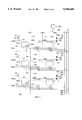
- FIG. 1a block diagram of a circuit for providing 100% controllability and observability of function circuit modules in a logic array integrated circuit according to a first embodiment of the present invention
- an array 10 of function circuit modules 12a-12iis shown.
- Array 10may be conceptually arranged as a plurality of rows and columns wherein modules 12a, 12b, and 12c form a first row; modules 12d, 12e, and 12f form a second row; and modules 12g, 12h, and 12i form a third row.
- modules 12a, 12d, and 12gform a first column; modules 12b, 12e, and 12h form a second column; and modules 12c, 12f, and 12i form a third column.
- FIG. 1contains nine such modules for purposes of illustrating the present invention, those of ordinary skill in the art will recognize that, in a practical embodiment fabricated according to the principles disclosed herein, an array may have hundreds or thousands of such modules.
- Function circuit modules 12a-12imay be configured from a wide range of circuits, including, but not limited to, hardwired integrated circuits and user-configurable logic modules of all types and description.
- logic modules 12a-12imay be similar to those described in U.S. Pat. No. 4,758,745 to El Gamal et al., and 4,910,417 to El Gamal et al., although those of ordinary skill in the art will readily be able to utilize other function circuit modules in the present invention.
- Function modules 12a-12iwill each have one or more inputs and at least one output (not shown in FIG. 1) for use in performing the functions assigned to the module and the overall circuit of which it is made a part.
- the overall circuitis realized by use of interconnections such as one or more hardwired metal interconnect layers formed by masking steps, or one of a number of available user programming techniques, such as antifuses or reconfigurable interconnect elements.
- each function module 12a-12imay be equipped with other inputs, outputs and circuit elements.
- the first function carried out by the present inventionis a control function implemented by the loading of a selected data test bit into a selected one of the function modules.
- the data test bitis presented to each of the modules 12a-12i via a common data test bit input (DTI) line 14.
- DTI line 14may be separated into more than one line for routing or other design convenience.
- a function module whose output is to be controlledis selected by addressing the selected module via an X select line (XSEL) and a Y select line (YSEL).
- XSELX select line
- YSELY select line
- XSEL 1 line 16is associated with the first row of the array
- XSEL 2 line 18is associated with the second row of the array
- XSEL 3 line 20is associated with the third row of the array.
- YSEL 1 line 22is associated with the first column of the array
- YSEL 2 line 24is associated with the second column of the array
- YSEL 3 line 26is associated with the third column of the array.
- a particular function module to be controlledmay be selected by activating its associated XSEL and YSEL lines.
- the XSEL and YSEL linesare active low logic level control lines, although those of ordinary skill in the art recognize that the active logic level for the control lines is somewhat arbitrary.
- function module 12eis selected when XSEL 2 line 18 and YSEL 2 line 24 are activated.
- XSEL 2 line 18 and YSEL 2 line 24are activated.
- the data test bit which is present on DTI line 14will be placed into the selected function module at an internal test bit node.
- YSEL lines 22, 24 and 26are controlled by transistors 34, 36, 38, and 40.
- Transistor 34is connected between YSEL 1 line and node 42.
- Transistor 36is connected between YSEL 2 line and node 42.
- Transistor 38is connected between YSEL 3 line and node 42.
- the gates of transistors 34, 36, and 38are connected to column address lines 46, 48, and 50.
- Transistor 40is connected between node 42 and a fixed voltage source, such as ground.
- the gate of transistor 40is controlled by a master CM signal on line 44.
- the XSEL and YSEL linesare preferably activated from the periphery of the circuit by well known selection circuitry, such as a conventional one-of-n decoder or shift register.
- DTI line 14may be controlled from off chip or internally by conventional circuitry. Since only one function module needs to be set at a time, DTI may be a global signal shared by all function modules. The control operation for function module 12 according to the present invention will be disclosed in more detail with reference to FIG. 2.
- FIG. 1illustrates RSEL 1 line 28 associated with the first row of the array, RSEL 2 line 30 associated with the second row in the array, and RSEL 3 line 32 associated with the third row in the array.
- RSEL 1 line 28associated with the first row of the array
- RSEL 2 line 30associated with the second row in the array
- RSEL 3 line 32associated with the third row in the array.
- the same YSEL lines 22, 24, and 26which are used to select a function module during control mode are used in the observe mode as output sense lines to observe the output of the function module.
- the selection of which column line YSEL to observe when the RSEL line associated with a particular row is activeis made by using transistors 52, 54, and 56, which are connected between their respective column YSEL lines and a common sense line 58.
- Sense line 58drives a sense amplifier and output buffer 60 which is connected to I/O pad 62.
- Transistors 64, 66, and 68are connected between transistors 52, 54, and 56, respectively, and ground.
- the gates of transistors 64, 66, and 68are connected to YSEL lines 22, 24, and 26.
- Each of transistors 64, 66, and 68senses (and inverts) the state of the YSEL line to which its gate is connected.
- the gates of transistors 52, 54, and 56are connected to column-observe select lines 70, 72, and 74 which can be decoded by conventional circuitry such as one-of-n decoders or shift registers. If one of transistors 52, 54, and 56 is turned on, the inverted state of the YSEL line with which it is associated will be presented at I/O pad 62.
- P-channel current source transistor 76is shown connected to each YSEL line and acts as a well-known pullup load to maintain a high logic level on the line in the absence of action by one of the devices connected to the line which would pull it to a low logic level.
- FIG. 2a schematic of a portion of a typical function module circuit 12, with which the present invention may be used, is shown containing the additional circuitry necessary to implement the present invention as described in FIG. 1.
- Each functional moduleincludes module inputs 80, 82, 84, 86, 88, and 90 which drive multiplexers 92 and 94.
- the output from either multiplexer 92 or 94is selected using transistors 96 and 98, driven by NOR gates 100 and 102.
- One input of NOR gate 100is driven by module input-104.
- Output buffers 106 and 108are used as is known in the art.
- function module 12appears at node 110.
- the operation of function modules like the one thus far described with reference to FIG. 2may be better understood with reference to U.S. Pat. Nos. 4,758,745 to El Gamal et al., and 4,910,417 to El Gamal et al.
- function module described hereinis merely illustrative of one environment into which the present invention may be placed, and that the invention is not limited to use with the illustrative function module shown in FIG. 2.
- a transistor switch 112is connected between DTI line 14 and an existing internal node 114 inside function module 12. Internal node 114 functions as a data test input node for the function module 12, and transistor 112 serves as a means to place the signal from DTI line 14 into the function module circuitry.
- the gate of transistor 112is driven from the output of NOR gate 116.
- NOR gate 116is driven from the XSEL and YSEL lines 118 and 120 which together select the particular function module 12 to be controlled.
- the output of NOR gate 116is high whenever the XSEL and YSEL lines 118 and 120 are simultaneously low.
- the output of NOR gate 116drives the other input of NOR gate 100.
- NOR gate 116When the output of NOR gate 116 is high, the outputs of NOR gates 100 and 102 are low, thus turning off transistors 96 and 98 to isolate node 114 from the input portion of function module 12. Since the output of NOR gate 116 is also connected to the gate of transistor 112, the same action which isolates the input section of function module 12 from node 114 also connects the data test input line 14 to node 114, thus placing the data test bit then present on that line on node 114 and also on output node 110 of function module 12 through output buffers 106 and 108.
- Two output read transistors 122 and 124are connected in series between YSEL line 120 and ground. These transistors are used during the observe mode of the present invention.
- the gate of the first output read transistor 122is connected to RSEL line 126.
- the gate of second output read transistor 124is connected to output node 110 of function module 12.
- function module 12has been configured as a sequential function, such as a latch, as shown by dashed line feedback connection 128 between output node 110 and input 80 of function module 12, the data placed onto internal node 114 will be latched into the function module and will remain there until other action is taken.
- a sequential functionsuch as a latch
- the data test bitmay not be retained.
- the real benefit of the control operationis obtained when it is applied to a function module which is configured as a sequential element, latch, or flip-flop stage.
- the control functionis applied to this function module as described above when it is in its recirculate mode, i.e., feeding back its output value to its input and thereby latching and maintaining its data.
- the control mechanismmay be deactivated and then used to control another latch stage or proceed with the observe function while the stimulus data is preserved in the latch. This is how auto test generation software works.
- Any latch or flip-flop stagemay be controlled by the above control scheme by selecting the appropriate control and test input signals as discussed above.
- controlling sequential elementsis the key ingredient in any test scheme, since the sequential elements define all the various states of the circuit.
- Combinatorial pathsare easily analyzed and vectors generated to test them.
- Combinatorial circuits which receive their input stimulus from input padscan easily be tested with test vectors.
- Combinatorial circuits which are buried deeper in the circuitneed to obtain their input stimuli from sequential elements in the circuit as well as from primary circuit inputs. Testing such circuits thus depends on the present state of the circuit.
- the appropriate statemay be loaded into the circuit.
- the entire circuitmay be tested by application of all the vectors needed using the combinatorial and sequential test stimuli until the test coverage of the circuit is complete.
- the outputs of the circuit elementsmay be observed and verified against expected circuit response.
- internal circuit nodessuch as function module outputs not directly connected to output pads may be observed. It may be advantageous or necessary to observe internal nodes, particularly those associated with sequential elements during the test operation and compare them with expected results.
- FIGS. 1 and 2are capable of controlling and observing internal nodes of integrated circuits. However, it is apparent that only one node at a time may be observed. Such a system, while useful, would present a testing throughput problem in a real world application where large production volumes of integrated circuits having several hundred or thousand rows and columns of function modules must be tested.
- FIG. 3ais a block diagram of circuitry useful with the present invention for supplying the results observed at a single point in time for a plurality of function modules.
- flip-flop circuits 130, 132, and 134arranged as a parallel to serial converter register as is well known in the art, have data inputs connected to YSEL lines 22, 24, and 26, respectively, of array 10. They are daisy chained together and are driven from a common clock line 136.
- Clock line 136may be driven from an external clock I/O pin on the integrated circuit, which may be selectively enabled by known methods during testing.
- a common data load line 138is used to load information from all YSEL lines to which the parallel to serial converter register is connected.
- Data load line 138may be driven from an external signal at an I/O pin on the integrated circuit, which may be selectively enabled by known methods during testing.
- the clock lineis activated and the data is clocked from the flip flops in serial form into output buffer 140 and to I/O pad 142. It is possible for the contents of an entire array to be shifted out one row at a time in this manner if necessary, thus providing a complete observation of the logic states of all nodes at the point in time that the latch command was given on data load line 138.
- FIG. 3bAnother variation of the scheme shown in FIG. 3a is illustrated in FIG. 3b, in which the results register is configured as a linear feedback shift register.
- the results registeris configured as a linear feedback shift register.
- Using a linear feedback shift registerresults in compressing and encoding the test results in a unique compact signature that can be shifted out and compared with an expected signature after the test has been completed.
- the technique illustrated in FIG. 3bfurther reduces overall circuit test times.
- the feedback connections in the linear feedback shift registerare selected according to a mathematical polynomial so that when the test is completed the register contains a unique pattern which only occurs when the circuit is functioning properly.
- Linear feedback shift registers, and their use for these purposes, as well as selection of polynomials for use in the tests described,are within the scope of one of ordinary skill in the art.
- FIG. 4aa block diagram of an embodiment of a circuit for carrying out a second aspect of the present invention is shown.
- the circuit shown in block diagram form in FIG. 4aallows 100% observability and 100% controllability of the function module.
- a function module 200includes an input section 202, which may perform, for example, combinatorial logic functions, sequential functions, or even analog functions.
- Input section 202includes inputs IN 1 , IN 2 , IN 3 , and IN 4 , shown respectively at reference numerals 204, 206, 208, and 210. While four inputs are shown, those of ordinary skill in the art will recognize that the number of inputs will vary depending on the intended function of input section 202.
- First latch 212may be one of a number of common data elements used to latch data, or, in the case of analog circuitry, may include a sample/hold amplifier or the like. First latch 212 is activated, as is known in the art, by a control input line 214 connected to a control signal C1. The output of first latch 212 is connected to an internal node 216 via a switch 218.
- a data test input (DTI) line 220connected to from a source of data test information shown as DTI, may be used to place data test information onto internal node 216 by activating address decoder 222 via its XSEL and YSEL lines 224 and 226, respectively.
- Second latch 228is activated, as is known in the art, by a control input line 230 connected to a control signal C2. Control signal C2 may also be used to open switch 218 to disconnect input section 202 from output section 232 of function module 200 as will be disclosed herein.
- Output section 232may include an output buffer, additional combinational or sequential logic or analog circuitry, or may simply be a direct connection, depending on the function of function module 200 and whether the output of second latch 228 is itself buffered.
- the output of output section 232is connected to at least one output lead 234 of function module 200.
- First and second latches 212 and 228may be configured as pass-through devices when their control inputs C1 and C2 are unactivated. When so configured, the operation of function module 200 is unaffected by the presence of the circuitry of the present invention.
- Probe circuitry 236is connected to output line 234 of function module 200 and serves to route the output value obtained from function module 200 to external diagnostic circuitry.
- the probe circuit 236is activated by YSEL line 226, although those of ordinary skill in the art will recognize that other schemes could be utilized.
- Probe circuit 236may be used to provide 100% observability of the outputs of all function modules 200 in an integrated circuit array.
- the output value for function module 200appears as an output of probe circuit 236 on XSEN line 238.
- XSEN lineIn an actual embodiment fabricated as a part of an integrated circuit, there will be a plurality of XSEN lines and a number of function modules 200 will be connected to each. XSEN line.
- YSEL lineWhen a particular YSEL line is activated, all probe circuits 236 associated with function modules 200 connected to that YSEL line will pass the values present on the outputs of their respective function modules to their respective XSEN lines. Circuits like those disclosed in FIGS. 3a and 3b may then be used to carry the data values off chip for analysis.
- the circuit of FIG. 4amay be used to provide 100% controllability of the function module 200. This circuit may also be used to retain the output state of input section 202 for diagnostic purposes.
- the output 234 of function block 200may be controlled by disconnecting output section 232 from input section 202 and placing a value from DTI input line 220 onto internal node 216 and latching it into second latch 228.
- Function module 200is selected for control by activating its XSEL and YSEL lines 224 and 226, thus passing the data value from DTI line 220 through address decoder 222 onto node 216.
- C2 input 230is activated, latching the data test value into second latch 228, and switch 218 (connected to C2 line 230) opens, disconnecting input section 202 from internal node 216 and output section 232.
- the value appearing at the output of input section 202 of function module 200 as a result of particular data values placed on inputs 204, 206, 208, and 210may be retained indefinitely in function module 200 by latching it into first latch 212 by using control line 214 (C1). Once new data has been loaded into first latch 212 by activating C1, this data may be latched into second latch 228 by activating C2. This enables observation of the new data.
- FIG. 4billustrative circuitry for implementing the block diagram circuit of FIG. 4a is shown. Where like elements are shown, the reference numerals in FIGS. 4a and 4b are the same.
- data test bit retentionis provided for a logic array integrated circuit. Data test bit retention allows placement and retention of a selected data test bit at the output node of a function circuit module regardless of whether that circuit is configured as a combinatorial or sequential circuit.
- a function circuit module 200may include input section function block 202, having inputs 204 and 206, 208, and 210. Only four inputs are shown for the purposes of illustrating the principles of the present invention, but those of ordinary skill in the art will recognize that particular design considerations will dictate how many inputs such a function block actually has.
- function block 202may include combinatorial logic, such as is disclosed in the embodiment of FIG. 2, or may include other circuits.
- the output of function block 202is connected to a node 240 internal to the function module.
- a first latchcomprising P-channel transistor 242, N-channel transistors 244 and 246 and inverter 248 has its input connected to node 240.
- the gate of N-channel transistor 244is connected to a control line C1 214.
- Control line C1 214is also connected to input section function block 202 and acts to isolate the output of function block 202 at node 240 from its input.
- control line 214 C1is held low. This action connects function block 202 to node 240 in one of numerous well known ways (e.g., as described above), and also configures the first latch as a pass through by turning off N-channel transistor 244.
- N-channel transistor 250is connected between the output of the first latch and the input of a second latch comprising P-channel transistor 252, N-channel transistors 254 and 256, and inverter 258.
- the gate of N-channel transistor 254is connected to a control line C2 230
- Control line C2 230is also connected to the gate of N-channel transistor 250 through inverter 260.
- the output of the second latchis connected to output node 234 through inverter buffer 262.
- control line C2 230is held low. This action turns on N-channel transistor 250, connecting the output of the first latch to the input of the second latch, and configures the second latch as a pass through by turning off N-channel transistor 254.
- N-channel transistors 264 and 266are connected in series between the input to the second latch and a DTI (data test input) line 220.
- the gate of N-channel transistor 264is connected to an XSEL line 224.
- the gate of N-channel transistor 266is connected to a YSEL line 226.
- XSEL line 224 and YSEL line 226are held low and transistors 264 and 266 are turned off. Data on DTI line 220 is thus inhibited from entering the module 200.
- N-channel transistors 268 and 270are connected between a fixed voltage, such as ground, and an XSEN line 238.
- the gate of N-channel transistor 268is connected to output node 234 of functional circuit module 200 and the gate of N-channel transistor 270 is connected to YSEL line 226.
- N-channel transistor 270is off because YSEL line 226 is held low.
- the output state of the circuit shown in FIG. 4bmay be easily observed by raising YSEL line 226.
- the logic state of output node 234will appear inverted on XSEN line 238 because of the action of N-channel transistors 268 and 270. If both output node 234 and YSEL line 226 are high, XSEN line 238 will be pulled to ground. If YSEL line 226 is high but output node 234 is low, XSEN line 238 will remain high.
- a small pullup devicemay be connected to XSEN line 238 to supply enough current to keep its voltage at a logic high state.
- all of the XSEL lines and YSEL lines in an integrated circuit containing the present inventionmay be controlled by peripheral circuits in a manner well known in the art.
- output node 234can be controlled.
- Control line C2 230is brought high, turning off N-channel transistor 250 and disconnecting the input section function block 202 and first latch from the second latch and output node 234.
- a selected logic levelmay then be placed on the input of the second latch by raising XSEL line 224 and YSEL line 226 to a high voltage and placing the desired logic level on DTI line 220. Because control line C2 230 has turned on N-channel transistor 254 in the second latch, whatever logic level appears on DTI line 220 will be latched at the output of the second latch and will appear uninverted at output node 234.
- output node 234will remain latched with the previous data test bit until either transistors 264 and 266 are turned on again and a new data test bit is presented at DTI input line 220, or line 230 (C2) is brought low, turning on transistor 250, turning off transistor 254, reconnecting the first latch to the second latch through transistor 250.
- control line 214is raised high to turn on N-channel transistor 244, simultaneously disconnecting the input section function block from node 240, resulting in the latching of the logic state which was present in input section function block 202.
- FIG. 4bcan be made to operate like the embodiment of FIGS. 1 and 2 by holding control line 214 (C1) low at all times and only raising control line 230 (C2) when test data on DTI line 220 is being introduced through transistors 264 and 266.
- FIG. 5is a block diagram of circuitry according to the present invention and illustrates by example the 100% controllability feature of the present invention.
- An array 300 of logic function circuit modules 302a-302iwhich may be conceptually arranged as a plurality of rows and columns, wherein modules 302a, 302b, and 302c form a first row; modules 302d, 302e, and 302f form a second row; and modules 302g, 302h, and 302i form a third row.
- modules 302a, 302d, and 302gform a first column; modules 302b, 302e, and 302h form a second column; and modules 302c, 302f, and 302i form a third column.
- logic function circuit modules 302a-302imay be configured from a wide variety of circuits.
- the size of the array depicted in FIG. 5is illustrative only for the purposes of illustrating the invention and, from the disclosure herein, those of ordinary skill in the art will understand how to construct an array of any size.
- Each of logic function circuit modules 302a-302iwill have a plurality of inputs (two are shown for purposes of illustration) and at least one output for use in performing the functions assigned to the module and the overall circuit of which it is a part.
- the overall circuitis realized by the use of interconnections between the inputs and the outputs of the logic function circuit modules utilized as circuit components. These interconnections may be made using mask-defined metal layers or by any technique for establishing user-defined interconnections.
- output 304 of module 302ais shown connected to first input 306 of module 302e via interconnect line 308.
- output 310 of module 302gis shown connected to second input 312 of module 302e via interconnect line 314.
- XSEL 1 -XSEL 3 linesshown at reference numerals 316, 318, and 320, respectively, and YSEL 1 -YSEL 3 lines, shown at reference numerals 322, 324, and 326, respectively, may be used to select one or more modules for control or observation in the manner disclosed herein with respect to FIGS. 3 and 4.
- Lines C1 (shown at reference numeral 328) and C2 (shown at reference numeral 330)are global control lines for the first and second latches of the function modules as described previously with reference to FIG. 4.
- DTI line 332is also a global data test input line for all of the modules, and is used to place selected data test bits into selected modules.
- XSEN lines XSEN 1 -XSEN 3are sense lines for reading out the logic state at the output nodes of selected modules and may be connected to transistors 340, which act as well-known pullup loads.
- Loadable flip-flops 342, 344, and 346are connected as a serial shift register and are used to transport the test data from the XSEN lines 334, 336, and 338 through buffer 348 to I/O pad 350 for observation and evaluation as is shown in FIG. 3a, although those of ordinary skill will recognize that other configurations, such as that of FIG. 3b or other similarly functioning circuits, could also be utilized.
- a transistor pairis used to place output test data bits from the modules into each of flip-flops 342, 344, and 346.
- Transistor 352has its gate connected to XSEN 1 line 334, its source connected to ground, and its drain connected to the source of transistor 354.
- the drain of transistor 354is connected to the data load input of flip-flop 342.
- transistor 356has its gate connected to XSEN 2 line 336, its source connected to ground, and its drain connected to the source of transistor 358.
- the drain of transistor 358is connected to the data load input of flip-flop 344.
- transistor 360has its gate connected to XSEN 3 line 338, its source connected to ground, and its drain connected to the source of transistor 362.
- the drain of transistor 362is connected to the data load input of flip-flop 346.
- the gates of transistors 354, 358, and 362may be connected to decoding control lines which can be driven using conventional decoding circuitry, such as shift registers or one-of-n decoders.
- module 302eit may be used to verify the functionality of module 302e.
- the outputs of modules 302a, and 302gare controlled to place desired test data bits at the first and second inputs of module 302e, and then the output of module 302e is observed.
- C2 line 330is first brought high, enabling the second latch for all function modules in the array.
- Module 302amay then be selected by bringing XSEL 1 line 316 and YSEL 2 line 322 high.
- the selected data test bit appearing on DTI line 332will be latched and retained at the output of module 302a.
- Module 302gmay then be selected by bringing XSEL 3 line 320 and YSEL 1 line 322 high.
- the selected data test bit appearing on DTI line 332will be latched and retained at the output of module 302g. If identical test bits are to be loaded into modules 302a, and 302g, this may be accomplished by simultaneously bringing the XSEL 1 line 316, XSEL 3 line 320, and YSEL 1 line 322 high.
- C2 line 330remains high and Cl line 328 is brought high to enable the first latch in all of the function modules in the array.
- Cl line 328is brought high to enable the first latch in all of the function modules in the array.
- C1 line 328is brought high, the new logic state of module 302e is latched into its first latch.
- C2 line 330is then brought low to transfer the new logic state to the output of module 302e.
- Module 302emay then be selected for observation by bringing YSEL 2 line 324 high, placing the inverted logic state of the output of module 302e on the XSEN 2 line 336.
- the gate of transistor 358is turned on and the output test data is loaded into flip-flop 344 and clocked out through buffer 348 to I/O pad 350.
- Multiple node controlallows the setting up (control) of the output nodes of more than one function circuit module which are connected to the inputs of another function circuit module, thus allowing the control of the several inputs of a single function circuit module.
- This featureadds versatility to control-observe testing of function modules in a logic array integrated circuit.
Landscapes
- Engineering & Computer Science (AREA)
- General Engineering & Computer Science (AREA)
- Physics & Mathematics (AREA)
- General Physics & Mathematics (AREA)
- Tests Of Electronic Circuits (AREA)
- Design And Manufacture Of Integrated Circuits (AREA)
Abstract
Description
Claims (6)
Priority Applications (1)
| Application Number | Priority Date | Filing Date | Title |
|---|---|---|---|
| US08/158,977US5528600A (en) | 1991-01-28 | 1993-11-30 | Testability circuits for logic arrays |
Applications Claiming Priority (3)
| Application Number | Priority Date | Filing Date | Title |
|---|---|---|---|
| US64626891A | 1991-01-28 | 1991-01-28 | |
| US91961992A | 1992-07-24 | 1992-07-24 | |
| US08/158,977US5528600A (en) | 1991-01-28 | 1993-11-30 | Testability circuits for logic arrays |
Related Parent Applications (1)
| Application Number | Title | Priority Date | Filing Date |
|---|---|---|---|
| US91961992ADivision | 1991-01-28 | 1992-07-24 |
Publications (1)
| Publication Number | Publication Date |
|---|---|
| US5528600Atrue US5528600A (en) | 1996-06-18 |
Family
ID=46248888
Family Applications (3)
| Application Number | Title | Priority Date | Filing Date |
|---|---|---|---|
| US08/158,977Expired - LifetimeUS5528600A (en) | 1991-01-28 | 1993-11-30 | Testability circuits for logic arrays |
| US08/303,045Expired - LifetimeUS5614818A (en) | 1991-01-28 | 1994-09-08 | Testability circuits for logic circuit arrays |
| US08/722,355Expired - Fee RelatedUS5804960A (en) | 1991-01-28 | 1996-09-27 | Circuits for testing the function circuit modules in an integrated circuit |
Family Applications After (2)
| Application Number | Title | Priority Date | Filing Date |
|---|---|---|---|
| US08/303,045Expired - LifetimeUS5614818A (en) | 1991-01-28 | 1994-09-08 | Testability circuits for logic circuit arrays |
| US08/722,355Expired - Fee RelatedUS5804960A (en) | 1991-01-28 | 1996-09-27 | Circuits for testing the function circuit modules in an integrated circuit |
Country Status (1)
| Country | Link |
|---|---|
| US (3) | US5528600A (en) |
Cited By (21)
| Publication number | Priority date | Publication date | Assignee | Title |
|---|---|---|---|---|
| US5751163A (en)* | 1996-04-16 | 1998-05-12 | Lattice Semiconductor Corporation | Parallel programming of in-system (ISP) programmable devices using an automatic tester |
| US5764574A (en)* | 1996-06-20 | 1998-06-09 | Nevill; Leland R. | Method and apparatus for back-end repair of multi-chip modules |
| US5804960A (en) | 1991-01-28 | 1998-09-08 | Actel Corporation | Circuits for testing the function circuit modules in an integrated circuit |
| US5821771A (en)* | 1996-05-21 | 1998-10-13 | Altera Corporation | Method and apparatus for monitoring or forcing an internal node in a programmable device |
| US5859543A (en)* | 1996-06-21 | 1999-01-12 | Quicklogic Corporation | Programming architecture for a programmable integrated circuit employing antifuses |
| US5872448A (en)* | 1991-06-18 | 1999-02-16 | Lightspeed Semiconductor Corporation | Integrated circuit architecture having an array of test cells providing full controlability for automatic circuit verification |
| US5892370A (en)* | 1996-06-21 | 1999-04-06 | Quicklogic Corporation | Clock network for field programmable gate array |
| WO1999030236A1 (en)* | 1997-12-05 | 1999-06-17 | Lightspeed Semiconductor Corporation | TEST CIRCUITRY FOR ASICs |
| WO1999052034A1 (en)* | 1998-04-02 | 1999-10-14 | Lightspeed Semiconductor Corporation | Integrated circuit architecture having an array of test cells providing full controllability for automatic circuit verification |
| US6028444A (en)* | 1996-06-21 | 2000-02-22 | Quicklogic Corporation | Three-statable net driver for antifuse field programmable gate array |
| US6101074A (en)* | 1996-06-21 | 2000-08-08 | Quicklogic Corporation | Power-up circuit for field programmable gate arrays |
| US6169416B1 (en) | 1998-09-01 | 2001-01-02 | Quicklogic Corporation | Programming architecture for field programmable gate array |
| US6346427B1 (en) | 1999-08-18 | 2002-02-12 | Utmc Microelectronic Systems Inc. | Parameter adjustment in a MOS integrated circuit |
| US6426650B1 (en) | 1999-12-28 | 2002-07-30 | Koninklijke Philips Electronics, N.V. | Integrated circuit with metal programmable logic having enhanced reliability |
| US6611932B2 (en) | 1997-12-05 | 2003-08-26 | Lightspeed Semiconductor Corporation | Method and apparatus for controlling and observing data in a logic block-based ASIC |
| US20040177298A1 (en)* | 1995-12-22 | 2004-09-09 | Farnworth Warren M. | Device and method for testing integrated circuit dice in an integrated circuit module |
| US20040201395A1 (en)* | 2003-03-07 | 2004-10-14 | Manfred Proll | Test apparatus for testing integrated modules and method for operating a test apparatus |
| DE102006047262A1 (en)* | 2006-10-04 | 2008-04-10 | Endress + Hauser Gmbh + Co. Kg | Method for testing an electronic unit |
| US20170269136A1 (en)* | 2016-03-16 | 2017-09-21 | Intel Corporation | Technologies for verifying a de-embedder for interconnect measurement |
| US11115024B2 (en)* | 2019-09-12 | 2021-09-07 | Kabushiki Kaisha Toshiba | Integrated circuit, test method for testing integrated circuit, and electronic device |
| US11403452B2 (en)* | 2015-10-20 | 2022-08-02 | Synopsys, Inc. | Logic yield learning vehicle with phased design windows |
Families Citing this family (19)
| Publication number | Priority date | Publication date | Assignee | Title |
|---|---|---|---|---|
| NL1006239C2 (en)* | 1997-06-05 | 1998-12-08 | Koninkl Kpn Nv | Transfer device with an electrical or optical signal bus. |
| US5991890A (en)* | 1998-04-16 | 1999-11-23 | Lsi Logic Corporation | Device and method for characterizing signal skew |
| ITTO980467A1 (en)* | 1998-05-29 | 1999-11-29 | St Microelectronics Srl | ADDITIONAL TEST CIRCUIT FOR THE MEASUREMENT OF DELAY TIMES IN CIRCUITS NOT DIRECTLY ACCESSIBLE |
| US6353634B1 (en)* | 1998-12-17 | 2002-03-05 | The United States Of America As Represented By The Secretary Of The Navy | Video decoder using bi-orthogonal wavelet coding |
| JP2000214220A (en)* | 1999-01-19 | 2000-08-04 | Texas Instr Inc <Ti> | On-chip module, and system and method for testing interconnection between on-chip modules |
| US6845249B1 (en)* | 1999-05-24 | 2005-01-18 | Sierra Wireless, Inc. | Analog test output switchably connected to PCMCIA connector pin |
| US6831474B2 (en)* | 2000-03-10 | 2004-12-14 | Infineon Technologies Ag | Apparatus and method for testing a plurality of electrical components that are coupled to one another |
| US6633613B1 (en)* | 2000-06-02 | 2003-10-14 | The United States Of America As Represented By The Secretary Of The Navy | Digital circuit for formatting and compressing radar video data |
| JP4212224B2 (en)* | 2000-07-10 | 2009-01-21 | 株式会社東芝 | Semiconductor integrated circuit |
| US6683467B1 (en)* | 2000-09-29 | 2004-01-27 | Intel Corporation | Method and apparatus for providing rotational burn-in stress testing |
| DE10110777A1 (en)* | 2001-03-07 | 2002-09-12 | Philips Corp Intellectual Pty | Arrangement and method for testing integrated circuits |
| US6476631B1 (en)* | 2001-06-29 | 2002-11-05 | Lsi Logic Corporation | Defect screening using delta VDD |
| DE10241385A1 (en)* | 2002-09-06 | 2004-03-25 | Infineon Technologies Ag | Integrated circuit for mobile radio equipment having function blocks with individual control systems |
| US20040051550A1 (en)* | 2002-09-12 | 2004-03-18 | Ma David Suitwai | Semiconductor die isolation system |
| US7710136B2 (en)* | 2004-11-29 | 2010-05-04 | Nxp B.V. | Intergrated circuit self-test architecture |
| US8161469B1 (en)* | 2005-12-13 | 2012-04-17 | Altera Corporation | Method and apparatus for comparing programmable logic device configurations |
| US7475164B2 (en)* | 2006-02-28 | 2009-01-06 | International Business Machines Corporation | Apparatus, system, and method for automated device configuration and testing |
| DE102007016622A1 (en)* | 2007-04-05 | 2008-10-09 | Qimonda Ag | Semiconductor device test method and test system with reduced number of test channels |
| US9921683B2 (en)* | 2012-05-30 | 2018-03-20 | Silicon Laboratories Inc. | Detection of defects in touch sensors |
Citations (44)
| Publication number | Priority date | Publication date | Assignee | Title |
|---|---|---|---|---|
| US3995215A (en)* | 1974-06-26 | 1976-11-30 | International Business Machines Corporation | Test technique for semiconductor memory array |
| US4255748A (en)* | 1979-02-12 | 1981-03-10 | Automation Systems, Inc. | Bus fault detector |
| US4357703A (en)* | 1980-10-09 | 1982-11-02 | Control Data Corporation | Test system for LSI circuits resident on LSI chips |
| US4418403A (en)* | 1981-02-02 | 1983-11-29 | Mostek Corporation | Semiconductor memory cell margin test circuit |
| US4435805A (en)* | 1981-06-04 | 1984-03-06 | International Business Machines Corporation | Testing of logic arrays |
| US4476560A (en)* | 1982-09-21 | 1984-10-09 | Advanced Micro Devices, Inc. | Diagnostic circuit for digital systems |
| US4525714A (en)* | 1982-12-03 | 1985-06-25 | Honeywell Information Systems Inc. | Programmable logic array with test capability in the unprogrammed state |
| US4583179A (en)* | 1981-12-29 | 1986-04-15 | Fujitsu Limited | Semiconductor integrated circuit |
| US4613970A (en)* | 1983-02-04 | 1986-09-23 | Hitachi, Ltd. | Integrated circuit device and method of diagnosing the same |
| US4625313A (en)* | 1984-07-06 | 1986-11-25 | Tektronix, Inc. | Method and apparatus for testing electronic equipment |
| US4669061A (en)* | 1984-12-21 | 1987-05-26 | Digital Equipment Corporation | Scannable flip-flop |
| US4672610A (en)* | 1985-05-13 | 1987-06-09 | Motorola, Inc. | Built in self test input generator for programmable logic arrays |
| US4701922A (en)* | 1984-09-04 | 1987-10-20 | Hitachi, Ltd. | Integrated circuit device |
| US4701921A (en)* | 1985-10-23 | 1987-10-20 | Texas Instruments Incorporated | Modularized scan path for serially tested logic circuit |
| US4703484A (en)* | 1985-12-19 | 1987-10-27 | Harris Corporation | Programmable integrated circuit fault detection apparatus |
| US4710933A (en)* | 1985-10-23 | 1987-12-01 | Texas Instruments Incorporated | Parallel/serial scan system for testing logic circuits |
| US4749947A (en)* | 1986-03-10 | 1988-06-07 | Cross-Check Systems, Inc. | Grid-based, "cross-check" test structure for testing integrated circuits |
| US4752729A (en)* | 1986-07-01 | 1988-06-21 | Texas Instruments Incorporated | Test circuit for VSLI integrated circuits |
| US4758745A (en)* | 1986-09-19 | 1988-07-19 | Actel Corporation | User programmable integrated circuit interconnect architecture and test method |
| US4764926A (en)* | 1984-12-21 | 1988-08-16 | Plessey Overseas Limited | Integrated circuits |
| US4768196A (en)* | 1986-10-28 | 1988-08-30 | Silc Technologies, Inc. | Programmable logic array |
| US4816757A (en)* | 1985-03-07 | 1989-03-28 | Texas Instruments Incorporated | Reconfigurable integrated circuit for enhanced testing in a manufacturing environment |
| US4857774A (en)* | 1986-09-19 | 1989-08-15 | Actel Corporation | Testing apparatus and diagnostic method for use with programmable interconnect architecture |
| US4878209A (en)* | 1988-03-17 | 1989-10-31 | International Business Machines Corporation | Macro performance test |
| US4912709A (en)* | 1987-10-23 | 1990-03-27 | Control Data Corporation | Flexible VLSI on-chip maintenance and test system with unit I/O cell design |
| US4926425A (en)* | 1987-06-11 | 1990-05-15 | Robert Bosch Gmbh | System for testing digital circuits |
| US4931722A (en)* | 1985-11-07 | 1990-06-05 | Control Data Corporation | Flexible imbedded test system for VLSI circuits |
| US4947395A (en)* | 1989-02-10 | 1990-08-07 | Ncr Corporation | Bus executed scan testing method and apparatus |
| US5012135A (en)* | 1989-05-12 | 1991-04-30 | Plus Logic, Inc. | Logic gates with a programmable number of inputs |
| US5032783A (en)* | 1985-10-23 | 1991-07-16 | Texas Instruments Incorporated | Test circuit and scan tested logic device with isolated data lines during testing |
| US5043986A (en)* | 1989-05-18 | 1991-08-27 | At&T Bell Laboratories | Method and integrated circuit adapted for partial scan testability |
| US5043985A (en)* | 1987-05-05 | 1991-08-27 | Industrial Technology Research Institute | Integrated circuit testing arrangement |
| US5047710A (en)* | 1987-10-07 | 1991-09-10 | Xilinx, Inc. | System for scan testing of logic circuit networks |
| US5054024A (en)* | 1989-08-09 | 1991-10-01 | Texas Instruments Incorporated | System scan path architecture with remote bus controller |
| US5065090A (en)* | 1988-07-13 | 1991-11-12 | Cross-Check Technology, Inc. | Method for testing integrated circuits having a grid-based, "cross-check" te |
| US5068605A (en)* | 1988-09-07 | 1991-11-26 | Hitachi, Ltd. | Semiconductor integrated circuit device and method of testing the same |
| US5072175A (en)* | 1990-09-10 | 1991-12-10 | Compaq Computer Corporation | Integrated circuit having improved continuity testability and a system incorporating the same |
| US5074710A (en)* | 1991-05-08 | 1991-12-24 | Northeastern University | Water gate array for current flow or tidal movement pneumatic harnessing system |
| US5083083A (en)* | 1986-09-19 | 1992-01-21 | Actel Corporation | Testability architecture and techniques for programmable interconnect architecture |
| US5130647A (en)* | 1990-01-23 | 1992-07-14 | Mitsubishi Denki Kabushiki Kaisha | Scan test circuit and semiconductor integrated circuit device using the same |
| US5155432A (en)* | 1987-10-07 | 1992-10-13 | Xilinx, Inc. | System for scan testing of logic circuit networks |
| US5221865A (en)* | 1991-06-21 | 1993-06-22 | Crosspoint Solutions, Inc. | Programmable input/output buffer circuit with test capability |
| US5223792A (en)* | 1986-09-19 | 1993-06-29 | Actel Corporation | Testability architecture and techniques for programmable interconnect architecture |
| US5349248A (en)* | 1992-09-03 | 1994-09-20 | Xilinx, Inc. | Adaptive programming method for antifuse technology |
Family Cites Families (131)
| Publication number | Priority date | Publication date | Assignee | Title |
|---|---|---|---|---|
| US3168697A (en)* | 1960-11-17 | 1965-02-02 | Sylvania Electric Prod | Method and apparatus for testing marginal failure of electronic systems |
| US3428945A (en)* | 1965-05-20 | 1969-02-18 | Bell Telephone Labor Inc | Error detection circuits |
| US3636518A (en)* | 1970-03-18 | 1972-01-18 | Gte Automatic Electric Lab Inc | Arrangement for detecting shorted diodes in selection matrices in core memories |
| US4004222A (en)* | 1974-11-20 | 1977-01-18 | Semi | Test system for semiconductor memory cell |
| JPS54121036A (en)* | 1978-03-13 | 1979-09-19 | Cho Lsi Gijutsu Kenkyu Kumiai | Method of testing function of logic circuit |
| FR2432175A1 (en)* | 1978-07-27 | 1980-02-22 | Cii Honeywell Bull | METHOD FOR TESTING A LOGIC SYSTEM AND LOGIC SYSTEM FOR IMPLEMENTING THE METHOD |
| US4253059A (en)* | 1979-05-14 | 1981-02-24 | Fairchild Camera & Instrument Corp. | EPROM Reliability test circuit |
| US4281398A (en)* | 1980-02-12 | 1981-07-28 | Mostek Corporation | Block redundancy for memory array |
| US4340857A (en)* | 1980-04-11 | 1982-07-20 | Siemens Corporation | Device for testing digital circuits using built-in logic block observers (BILBO's) |
| DE3015992A1 (en)* | 1980-04-25 | 1981-11-05 | Ibm Deutschland Gmbh, 7000 Stuttgart | PROGRAMMABLE LOGICAL ARRANGEMENT |
| US4479088A (en)* | 1981-01-16 | 1984-10-23 | Burroughs Corporation | Wafer including test lead connected to ground for testing networks thereon |
| US4409676A (en)* | 1981-02-19 | 1983-10-11 | Fairchild Camera & Instrument Corporation | Method and means for diagnostic testing of CCD memories |
| DE3135368A1 (en)* | 1981-09-07 | 1983-03-31 | Siemens AG, 1000 Berlin und 8000 München | METHOD AND ARRANGEMENT FOR FUNCTIONAL TESTING OF A PROGRAMMABLE LOGIC ARRANGEMENT |
| JPS5853775A (en)* | 1981-09-26 | 1983-03-30 | Fujitsu Ltd | IC memory test method |
| US4556840A (en)* | 1981-10-30 | 1985-12-03 | Honeywell Information Systems Inc. | Method for testing electronic assemblies |
| US4510572A (en)* | 1981-12-28 | 1985-04-09 | Data I/O Corporation | Signature analysis system for testing digital circuits |
| US4498172A (en)* | 1982-07-26 | 1985-02-05 | General Electric Company | System for polynomial division self-testing of digital networks |
| US4503536A (en)* | 1982-09-13 | 1985-03-05 | General Dynamics | Digital circuit unit testing system utilizing signature analysis |
| US4493078A (en)* | 1982-09-29 | 1985-01-08 | Siemens Corporation | Method and apparatus for testing a digital computer |
| US4513418A (en)* | 1982-11-08 | 1985-04-23 | International Business Machines Corporation | Simultaneous self-testing system |
| US4527272A (en)* | 1982-12-06 | 1985-07-02 | Tektronix, Inc. | Signature analysis using random probing and signature memory |
| JPS59107493A (en)* | 1982-12-09 | 1984-06-21 | Ricoh Co Ltd | EPROM memory device with test circuit |
| US4527115A (en)* | 1982-12-22 | 1985-07-02 | Raytheon Company | Configurable logic gate array |
| US4542340A (en)* | 1982-12-30 | 1985-09-17 | Ibm Corporation | Testing method and structure for leakage current characterization in the manufacture of dynamic RAM cells |
| US4503387A (en)* | 1982-12-30 | 1985-03-05 | Harris Corporation | A.C. Testing of logic arrays |
| GB2150696B (en)* | 1983-11-25 | 1988-09-01 | Mars Inc | Automatic test equipment |
| US4595875A (en)* | 1983-12-22 | 1986-06-17 | Monolithic Memories, Incorporated | Short detector for PROMS |
| US4601033A (en)* | 1984-01-16 | 1986-07-15 | Siemens Corporate Research & Suppport, Inc. | Circuit testing apparatus employing signature analysis |
| US4598401A (en)* | 1984-05-03 | 1986-07-01 | Siemens Corporate Research & Support, Inc. | Circuit testing apparatus employing signature analysis |
| US4703436A (en)* | 1984-02-01 | 1987-10-27 | Inova Microelectronics Corporation | Wafer level integration technique |
| US4601034A (en)* | 1984-03-30 | 1986-07-15 | Texas Instruments Incorporated | Method and apparatus for testing very large scale integrated memory circuits |
| US4779273A (en)* | 1984-06-14 | 1988-10-18 | Data General Corporation | Apparatus for self-testing a digital logic circuit |
| US4612630A (en)* | 1984-07-27 | 1986-09-16 | Harris Corporation | EEPROM margin testing design |
| US4638246A (en)* | 1984-09-21 | 1987-01-20 | Gte Laboratories Incorporated | Integrated circuit input-output diagnostic system |
| JPS61141022A (en)* | 1984-12-14 | 1986-06-28 | インタ−ナショナル ビジネス マシ−ンズ コ−ポレ−ション | Tester for keyboard interface circuit |
| US4728883A (en)* | 1985-03-15 | 1988-03-01 | Tektronix, Inc. | Method of testing electronic circuits |
| US4814646A (en)* | 1985-03-22 | 1989-03-21 | Monolithic Memories, Inc. | Programmable logic array using emitter-coupled logic |
| US4638243A (en)* | 1985-06-05 | 1987-01-20 | Monolithic Memories, Inc. | Short detector for fusible link array using single reference fuse |
| US4635261A (en)* | 1985-06-26 | 1987-01-06 | Motorola, Inc. | On chip test system for configurable gate arrays |
| US4698589A (en)* | 1986-03-21 | 1987-10-06 | Harris Corporation | Test circuitry for testing fuse link programmable memory devices |
| US5309091A (en) | 1986-09-19 | 1994-05-03 | Actel Corporation | Testability architecture and techniques for programmable interconnect architecture |
| US5365165A (en) | 1986-09-19 | 1994-11-15 | Actel Corporation | Testability architecture and techniques for programmable interconnect architecture |
| US5208530A (en) | 1986-09-19 | 1993-05-04 | Actel Corporation | Testability architecture and techniques for programmable interconnect architecture |
| US5341092A (en) | 1986-09-19 | 1994-08-23 | Actel Corporation | Testability architecture and techniques for programmable interconnect architecture |
| US4910417A (en)* | 1986-09-19 | 1990-03-20 | Actel Corporation | Universal logic module comprising multiplexers |
| US4766593A (en)* | 1986-12-22 | 1988-08-23 | Motorola, Inc. | Monolithically integrated testable registers that cannot be directly addressed |
| US4751679A (en)* | 1986-12-22 | 1988-06-14 | Motorola, Inc. | Gate stress test of a MOS memory |
| US4782487A (en)* | 1987-05-15 | 1988-11-01 | Digital Equipment Corporation | Memory test method and apparatus |
| JPS6432979A (en)* | 1987-07-29 | 1989-02-02 | Isuzu Motors Ltd | Dust-proof and mud-proof structure for frame of vehicle or the like |
| US4870346A (en)* | 1987-09-14 | 1989-09-26 | Texas Instruments Incorporated | Distributed pseudo random sequence control with universal polynomial function generator for LSI/VLSI test systems |
| JPH0820967B2 (en)* | 1987-09-25 | 1996-03-04 | 三菱電機株式会社 | Integrated circuit |
| US4855669A (en)* | 1987-10-07 | 1989-08-08 | Xilinx, Inc. | System for scan testing of logic circuit networks |
| US4835458A (en)* | 1987-11-09 | 1989-05-30 | Intel Corporation | Signature analysis technique for defect characterization of CMOS static RAM cell failures |
| FR2623653B1 (en)* | 1987-11-24 | 1992-10-23 | Sgs Thomson Microelectronics | METHOD FOR TESTING ELECTRICALLY PROGRAMMABLE MEMORY CELLS AND CORRESPONDING INTEGRATED CIRCUIT |
| JP2673298B2 (en)* | 1987-12-17 | 1997-11-05 | 三菱電機株式会社 | Semiconductor integrated circuit with self-test function |
| JP2986104B2 (en) | 1988-03-15 | 1999-12-06 | 株式会社東芝 | Information processing equipment self-test circuit |
| US5033048A (en)* | 1988-04-01 | 1991-07-16 | Digital Equipment Corporation | Memory selftest method and apparatus same |
| US4903266A (en)* | 1988-04-29 | 1990-02-20 | International Business Machines Corporation | Memory self-test |
| US4974184A (en)* | 1988-05-05 | 1990-11-27 | Honeywell Inc. | Maximum length pseudo-random test pattern generator via feedback network modification |
| US5103557A (en)* | 1988-05-16 | 1992-04-14 | Leedy Glenn J | Making and testing an integrated circuit using high density probe points |
| US5225771A (en) | 1988-05-16 | 1993-07-06 | Dri Technology Corp. | Making and testing an integrated circuit using high density probe points |
| US4929889A (en)* | 1988-06-13 | 1990-05-29 | Digital Equipment Corporation | Data path chip test architecture |
| DE3886038T2 (en) | 1988-07-13 | 1994-05-19 | Philips Nv | Storage device which contains a static RAM memory adapted for carrying out a self-test and integrated circuit which contains such a device as built-in static RAM memory. |
| NL8801835A (en)* | 1988-07-20 | 1990-02-16 | Philips Nv | METHOD AND APPARATUS FOR TESTING MULTIPLE POWER CONNECTIONS OF AN INTEGRATED CIRCUIT ON A PRINT PANEL |
| US5134584A (en)* | 1988-07-22 | 1992-07-28 | Vtc Incorporated | Reconfigurable memory |
| US5084874A (en)* | 1988-09-07 | 1992-01-28 | Texas Instruments Incorporated | Enhanced test circuit |
| JP2827229B2 (en)* | 1988-10-14 | 1998-11-25 | 日本電気株式会社 | Semiconductor integrated circuit |
| US5351247A (en) | 1988-12-30 | 1994-09-27 | Digital Equipment Corporation | Adaptive fault identification system |
| US5103450A (en)* | 1989-02-08 | 1992-04-07 | Texas Instruments Incorporated | Event qualified testing protocols for integrated circuits |
| US5001713A (en)* | 1989-02-08 | 1991-03-19 | Texas Instruments Incorporated | Event qualified testing architecture for integrated circuits |
| US4956602A (en)* | 1989-02-14 | 1990-09-11 | Amber Engineering, Inc. | Wafer scale testing of redundant integrated circuit dies |
| US4918378A (en)* | 1989-06-12 | 1990-04-17 | Unisys Corporation | Method and circuitry for enabling internal test operations in a VLSI chip |
| JPH081457B2 (en) | 1989-09-29 | 1996-01-10 | 株式会社東芝 | Testability circuits in digital integrated circuits. |
| US5101409A (en)* | 1989-10-06 | 1992-03-31 | International Business Machines Corporation | Checkboard memory self-test |
| US4991175A (en)* | 1989-10-06 | 1991-02-05 | Hewlett-Packard | Signature analysis |
| US5121394A (en)* | 1989-12-20 | 1992-06-09 | Bull Hn Information Systems Inc. | Method of organizing programmable logic array devices for board testability |
| US4963825A (en)* | 1989-12-21 | 1990-10-16 | Intel Corporation | Method of screening EPROM-related devices for endurance failure |
| US5157782A (en) | 1990-01-31 | 1992-10-20 | Hewlett-Packard Company | System and method for testing computer hardware and software |
| US5091908A (en)* | 1990-02-06 | 1992-02-25 | At&T Bell Laboratories | Built-in self-test technique for read-only memories |
| US5138619A (en)* | 1990-02-15 | 1992-08-11 | National Semiconductor Corporation | Built-in self test for integrated circuit memory |
| US5488615A (en) | 1990-02-28 | 1996-01-30 | Ail Systems, Inc. | Universal digital signature bit device |
| US5107501A (en)* | 1990-04-02 | 1992-04-21 | At&T Bell Laboratories | Built-in self-test technique for content-addressable memories |
| US5224101A (en) | 1990-05-16 | 1993-06-29 | The United States Of America As Represented By The Secretary Of The Air Force | Micro-coded built-in self-test apparatus for a memory array |
| US5173906A (en) | 1990-08-31 | 1992-12-22 | Dreibelbis Jeffrey H | Built-in self test for integrated circuits |
| US5258986A (en) | 1990-09-19 | 1993-11-02 | Vlsi Technology, Inc. | Tightly coupled, low overhead RAM built-in self-test logic with particular applications for embedded memories |
| US5097206A (en)* | 1990-10-05 | 1992-03-17 | Hewlett-Packard Company | Built-in test circuit for static CMOS circuits |
| DE69133311T2 (en) | 1990-10-15 | 2004-06-24 | Aptix Corp., San Jose | Connection substrate with integrated circuit for programmable connection and sample analysis |
| US5166604A (en) | 1990-11-13 | 1992-11-24 | Altera Corporation | Methods and apparatus for facilitating scan testing of asynchronous logic circuitry |
| US5367207A (en) | 1990-12-04 | 1994-11-22 | Xilinx, Inc. | Structure and method for programming antifuses in an integrated circuit array |
| US5222066A (en) | 1990-12-26 | 1993-06-22 | Motorola, Inc. | Modular self-test for embedded SRAMS |
| JPH0770240B2 (en) | 1990-12-27 | 1995-07-31 | 株式会社東芝 | Semiconductor integrated circuit |
| KR960007478B1 (en) | 1990-12-27 | 1996-06-03 | 가부시키가이샤 도시바 | Semiconductor Device and Manufacturing Method |
| US5130777A (en)* | 1991-01-04 | 1992-07-14 | Actel Corporation | Apparatus for improving antifuse programming yield and reducing antifuse programming time |
| US5528600A (en) | 1991-01-28 | 1996-06-18 | Actel Corporation | Testability circuits for logic arrays |
| US5317209A (en) | 1991-08-29 | 1994-05-31 | National Semiconductor Corporation | Dynamic three-state bussing capability in a configurable logic array |
| TW241346B (en) | 1991-10-15 | 1995-02-21 | Bull Hn Information Syst | |
| US5416784A (en) | 1991-10-28 | 1995-05-16 | Sequoia Semiconductor | Built-in self-test flip-flop with asynchronous input |
| US5347519A (en) | 1991-12-03 | 1994-09-13 | Crosspoint Solutions Inc. | Preprogramming testing in a field programmable gate array |
| US5357523A (en) | 1991-12-18 | 1994-10-18 | International Business Machines Corporation | Memory testing system with algorithmic test data generation |
| GR920100088A (en) | 1992-03-05 | 1993-11-30 | Consulting R & D Corp Koloni S | Transparent testing of integrated circuits. |
| US5241266A (en) | 1992-04-10 | 1993-08-31 | Micron Technology, Inc. | Built-in test circuit connection for wafer level burnin and testing of individual dies |
| US5457400A (en) | 1992-04-10 | 1995-10-10 | Micron Technology, Inc. | Semiconductor array having built-in test circuit for wafer level testing |
| US5237219A (en) | 1992-05-08 | 1993-08-17 | Altera Corporation | Methods and apparatus for programming cellular programmable logic integrated circuits |
| US5325054A (en) | 1992-07-07 | 1994-06-28 | Texas Instruments Incorporated | Method and system for screening reliability of semiconductor circuits |
| US5291079A (en) | 1992-07-23 | 1994-03-01 | Xilinx, Inc. | Configuration control unit for programming a field programmable gate array and reading array status |
| US5561367A (en) | 1992-07-23 | 1996-10-01 | Xilinx, Inc. | Structure and method for testing wiring segments in an integrated circuit device |
| US5617021A (en) | 1992-07-23 | 1997-04-01 | Xilinx, Inc. | High speed post-programming net verification method |
| US5383195A (en) | 1992-10-19 | 1995-01-17 | Motorola, Inc. | BIST circuit with halt signal |
| US5442640A (en) | 1993-01-19 | 1995-08-15 | International Business Machines Corporation | Test and diagnosis of associated output logic for products having embedded arrays |
| US5381419A (en) | 1993-03-01 | 1995-01-10 | At&T Corp. | Method and apparatus for detecting retention faults in memories |
| US5315177A (en) | 1993-03-12 | 1994-05-24 | Micron Semiconductor, Inc. | One time programmable fully-testable programmable logic device with zero power and anti-fuse cell architecture |
| US5371748A (en) | 1993-03-26 | 1994-12-06 | Vlsi Technology, Inc. | Technique and apparatus for testing an electrically programmable ROM embedded among other digital circuitry on an IC chip |
| US5360747A (en) | 1993-06-10 | 1994-11-01 | Xilinx, Inc. | Method of reducing dice testing with on-chip identification |
| EP0632468A1 (en) | 1993-06-30 | 1995-01-04 | International Business Machines Corporation | Fast data compression circuit for semiconductor memory chips including an abist structure |
| EP0632384A1 (en) | 1993-06-30 | 1995-01-04 | International Business Machines Corporation | High speed and programmable array clock generator circuit for abist semiconductor memory chips |
| US5493519A (en) | 1993-08-16 | 1996-02-20 | Altera Corporation | High voltage driver circuit with fast current limiting for testing of integrated circuits |
| US5414364A (en) | 1993-09-08 | 1995-05-09 | Actel Corporation | Apparatus and method for measuring programmed antifuse resistance |
| US5579326A (en) | 1994-01-31 | 1996-11-26 | Sgs-Thomson Microelectronics, Inc. | Method and apparatus for programming signal timing |
| US5453696A (en) | 1994-02-01 | 1995-09-26 | Crosspoint Solutions, Inc. | Embedded fuse resistance measuring circuit |
| US5539349A (en) | 1994-03-24 | 1996-07-23 | Hitachi Microsystems, Inc. | Method and apparatus for post-fabrication ascertaining and providing programmable precision timing for sense amplifiers and other circuits |
| US5550843A (en) | 1994-04-01 | 1996-08-27 | Xilinx, Inc. | Programmable scan chain testing structure and method |
| US5475815A (en) | 1994-04-11 | 1995-12-12 | Unisys Corporation | Built-in-self-test scheme for testing multiple memory elements |
| US5469396A (en) | 1994-06-07 | 1995-11-21 | Actel Corporation | Apparatus and method determining the resistance of antifuses in an array |
| US5485105A (en) | 1994-08-01 | 1996-01-16 | Texas Instruments Inc. | Apparatus and method for programming field programmable arrays |
| US5550842A (en) | 1994-10-28 | 1996-08-27 | Altera Corporation | EEPROM verification circuit with PMOS transistors |
| US5577050A (en) | 1994-12-28 | 1996-11-19 | Lsi Logic Corporation | Method and apparatus for configurable build-in self-repairing of ASIC memories design |
| US5608337A (en) | 1995-06-07 | 1997-03-04 | Altera Corporation | Method and apparatus of testing an integrated circuit device |
| US5621312A (en) | 1995-07-05 | 1997-04-15 | Altera Corporation | Method and apparatus for checking the integrity of a device tester-handler setup |
| US5627478A (en) | 1995-07-06 | 1997-05-06 | Micron Technology, Inc. | Apparatus for disabling and re-enabling access to IC test functions |
| US5651013A (en) | 1995-11-14 | 1997-07-22 | International Business Machines Corporation | Programmable circuits for test and operation of programmable gate arrays |
| US5689516A (en) | 1996-06-26 | 1997-11-18 | Xilinx, Inc. | Reset circuit for a programmable logic device |
- 1993
- 1993-11-30USUS08/158,977patent/US5528600A/ennot_activeExpired - Lifetime
- 1994
- 1994-09-08USUS08/303,045patent/US5614818A/ennot_activeExpired - Lifetime
- 1996
- 1996-09-27USUS08/722,355patent/US5804960A/ennot_activeExpired - Fee Related
Patent Citations (45)
| Publication number | Priority date | Publication date | Assignee | Title |
|---|---|---|---|---|
| US3995215A (en)* | 1974-06-26 | 1976-11-30 | International Business Machines Corporation | Test technique for semiconductor memory array |
| US4255748A (en)* | 1979-02-12 | 1981-03-10 | Automation Systems, Inc. | Bus fault detector |
| US4357703A (en)* | 1980-10-09 | 1982-11-02 | Control Data Corporation | Test system for LSI circuits resident on LSI chips |
| US4418403A (en)* | 1981-02-02 | 1983-11-29 | Mostek Corporation | Semiconductor memory cell margin test circuit |
| US4435805A (en)* | 1981-06-04 | 1984-03-06 | International Business Machines Corporation | Testing of logic arrays |
| US4583179A (en)* | 1981-12-29 | 1986-04-15 | Fujitsu Limited | Semiconductor integrated circuit |
| US4476560A (en)* | 1982-09-21 | 1984-10-09 | Advanced Micro Devices, Inc. | Diagnostic circuit for digital systems |
| US4525714A (en)* | 1982-12-03 | 1985-06-25 | Honeywell Information Systems Inc. | Programmable logic array with test capability in the unprogrammed state |
| US4613970A (en)* | 1983-02-04 | 1986-09-23 | Hitachi, Ltd. | Integrated circuit device and method of diagnosing the same |
| US4625313A (en)* | 1984-07-06 | 1986-11-25 | Tektronix, Inc. | Method and apparatus for testing electronic equipment |
| US4701922A (en)* | 1984-09-04 | 1987-10-20 | Hitachi, Ltd. | Integrated circuit device |
| US4669061A (en)* | 1984-12-21 | 1987-05-26 | Digital Equipment Corporation | Scannable flip-flop |
| US4764926A (en)* | 1984-12-21 | 1988-08-16 | Plessey Overseas Limited | Integrated circuits |
| US4816757A (en)* | 1985-03-07 | 1989-03-28 | Texas Instruments Incorporated | Reconfigurable integrated circuit for enhanced testing in a manufacturing environment |
| US4672610A (en)* | 1985-05-13 | 1987-06-09 | Motorola, Inc. | Built in self test input generator for programmable logic arrays |
| US4701921A (en)* | 1985-10-23 | 1987-10-20 | Texas Instruments Incorporated | Modularized scan path for serially tested logic circuit |
| US4710933A (en)* | 1985-10-23 | 1987-12-01 | Texas Instruments Incorporated | Parallel/serial scan system for testing logic circuits |
| US5032783A (en)* | 1985-10-23 | 1991-07-16 | Texas Instruments Incorporated | Test circuit and scan tested logic device with isolated data lines during testing |
| US4931722A (en)* | 1985-11-07 | 1990-06-05 | Control Data Corporation | Flexible imbedded test system for VLSI circuits |
| US4703484A (en)* | 1985-12-19 | 1987-10-27 | Harris Corporation | Programmable integrated circuit fault detection apparatus |
| US4749947A (en)* | 1986-03-10 | 1988-06-07 | Cross-Check Systems, Inc. | Grid-based, "cross-check" test structure for testing integrated circuits |
| US4752729A (en)* | 1986-07-01 | 1988-06-21 | Texas Instruments Incorporated | Test circuit for VSLI integrated circuits |
| US4857774A (en)* | 1986-09-19 | 1989-08-15 | Actel Corporation | Testing apparatus and diagnostic method for use with programmable interconnect architecture |
| US4758745A (en)* | 1986-09-19 | 1988-07-19 | Actel Corporation | User programmable integrated circuit interconnect architecture and test method |
| US5223792A (en)* | 1986-09-19 | 1993-06-29 | Actel Corporation | Testability architecture and techniques for programmable interconnect architecture |
| US4758745B1 (en)* | 1986-09-19 | 1994-11-15 | Actel Corp | User programmable integrated circuit interconnect architecture and test method |
| US5083083A (en)* | 1986-09-19 | 1992-01-21 | Actel Corporation | Testability architecture and techniques for programmable interconnect architecture |
| US4768196A (en)* | 1986-10-28 | 1988-08-30 | Silc Technologies, Inc. | Programmable logic array |
| US5043985A (en)* | 1987-05-05 | 1991-08-27 | Industrial Technology Research Institute | Integrated circuit testing arrangement |
| US4926425A (en)* | 1987-06-11 | 1990-05-15 | Robert Bosch Gmbh | System for testing digital circuits |
| US5047710A (en)* | 1987-10-07 | 1991-09-10 | Xilinx, Inc. | System for scan testing of logic circuit networks |
| US5155432A (en)* | 1987-10-07 | 1992-10-13 | Xilinx, Inc. | System for scan testing of logic circuit networks |
| US4912709A (en)* | 1987-10-23 | 1990-03-27 | Control Data Corporation | Flexible VLSI on-chip maintenance and test system with unit I/O cell design |
| US4878209A (en)* | 1988-03-17 | 1989-10-31 | International Business Machines Corporation | Macro performance test |
| US5065090A (en)* | 1988-07-13 | 1991-11-12 | Cross-Check Technology, Inc. | Method for testing integrated circuits having a grid-based, "cross-check" te |
| US5068605A (en)* | 1988-09-07 | 1991-11-26 | Hitachi, Ltd. | Semiconductor integrated circuit device and method of testing the same |
| US4947395A (en)* | 1989-02-10 | 1990-08-07 | Ncr Corporation | Bus executed scan testing method and apparatus |
| US5012135A (en)* | 1989-05-12 | 1991-04-30 | Plus Logic, Inc. | Logic gates with a programmable number of inputs |
| US5043986A (en)* | 1989-05-18 | 1991-08-27 | At&T Bell Laboratories | Method and integrated circuit adapted for partial scan testability |
| US5054024A (en)* | 1989-08-09 | 1991-10-01 | Texas Instruments Incorporated | System scan path architecture with remote bus controller |
| US5130647A (en)* | 1990-01-23 | 1992-07-14 | Mitsubishi Denki Kabushiki Kaisha | Scan test circuit and semiconductor integrated circuit device using the same |
| US5072175A (en)* | 1990-09-10 | 1991-12-10 | Compaq Computer Corporation | Integrated circuit having improved continuity testability and a system incorporating the same |
| US5074710A (en)* | 1991-05-08 | 1991-12-24 | Northeastern University | Water gate array for current flow or tidal movement pneumatic harnessing system |
| US5221865A (en)* | 1991-06-21 | 1993-06-22 | Crosspoint Solutions, Inc. | Programmable input/output buffer circuit with test capability |
| US5349248A (en)* | 1992-09-03 | 1994-09-20 | Xilinx, Inc. | Adaptive programming method for antifuse technology |
Cited By (40)
| Publication number | Priority date | Publication date | Assignee | Title |
|---|---|---|---|---|
| US5804960A (en) | 1991-01-28 | 1998-09-08 | Actel Corporation | Circuits for testing the function circuit modules in an integrated circuit |
| US6150807A (en)* | 1991-06-18 | 2000-11-21 | Lightspeed Semiconductor Corp. | Integrated circuit architecture having an array of test cells providing full controllability for automatic circuit verification |
| US5872448A (en)* | 1991-06-18 | 1999-02-16 | Lightspeed Semiconductor Corporation | Integrated circuit architecture having an array of test cells providing full controlability for automatic circuit verification |
| US7730372B2 (en) | 1995-12-22 | 2010-06-01 | Micron Technology, Inc. | Device and method for testing integrated circuit dice in an integrated circuit module |
| US7519881B2 (en) | 1995-12-22 | 2009-04-14 | Micron Technology, Inc. | Device and method for testing integrated circuit dice in an integrated circuit module |
| US20090027076A1 (en)* | 1995-12-22 | 2009-01-29 | Micron Technology, Inc. | Device and method for testing integrated circuit dice in an integrated circuit module |
| US20060244473A1 (en)* | 1995-12-22 | 2006-11-02 | Farnworth Warren M | Device and method for testing integrated circuit dice in an integrated circuit module |
| US7034560B2 (en) | 1995-12-22 | 2006-04-25 | Micron Technology, Inc. | Device and method for testing integrated circuit dice in an integrated circuit module |
| US20040177298A1 (en)* | 1995-12-22 | 2004-09-09 | Farnworth Warren M. | Device and method for testing integrated circuit dice in an integrated circuit module |
| US5751163A (en)* | 1996-04-16 | 1998-05-12 | Lattice Semiconductor Corporation | Parallel programming of in-system (ISP) programmable devices using an automatic tester |
| US5821771A (en)* | 1996-05-21 | 1998-10-13 | Altera Corporation | Method and apparatus for monitoring or forcing an internal node in a programmable device |
| US5764574A (en)* | 1996-06-20 | 1998-06-09 | Nevill; Leland R. | Method and apparatus for back-end repair of multi-chip modules |
| US5986469A (en)* | 1996-06-21 | 1999-11-16 | Quicklogic Corporation | Programmable integrated circuit having L-shaped programming power buses that extend along sides of the integrated circuit |
| US6028444A (en)* | 1996-06-21 | 2000-02-22 | Quicklogic Corporation | Three-statable net driver for antifuse field programmable gate array |
| US6081129A (en)* | 1996-06-21 | 2000-06-27 | Quicklogic Corporation | Field programmable gate array having testable antifuse programming architecture and method therefore |
| US6084428A (en)* | 1996-06-21 | 2000-07-04 | Quicklogic Corporation | Programmable integrated circuit having shared programming conductors between columns of logic modules |
| US6101074A (en)* | 1996-06-21 | 2000-08-08 | Quicklogic Corporation | Power-up circuit for field programmable gate arrays |
| US6130554A (en)* | 1996-06-21 | 2000-10-10 | Quicklogic Corporation | Programmable integrated circuit having a test circuit for testing the integrity of routing resource structures |
| US6018251A (en)* | 1996-06-21 | 2000-01-25 | Quicklogic Corporation | Programmable integrated circuit having parallel routing conductors coupled to programming drivers in different locations |
| US5966028A (en)* | 1996-06-21 | 1999-10-12 | Quicklogic Corporation | Programming architecture for a programmable integrated circuit employing test antifuses and test transistors |
| US6011408A (en)* | 1996-06-21 | 2000-01-04 | Quicklogic Corporation | Programmable integrated circuit having a routing conductor that is driven with programming current from two different programming voltage terminals |
| US5859543A (en)* | 1996-06-21 | 1999-01-12 | Quicklogic Corporation | Programming architecture for a programmable integrated circuit employing antifuses |
| US5892370A (en)* | 1996-06-21 | 1999-04-06 | Quicklogic Corporation | Clock network for field programmable gate array |
| US6611932B2 (en) | 1997-12-05 | 2003-08-26 | Lightspeed Semiconductor Corporation | Method and apparatus for controlling and observing data in a logic block-based ASIC |
| US6223313B1 (en) | 1997-12-05 | 2001-04-24 | Lightspeed Semiconductor Corporation | Method and apparatus for controlling and observing data in a logic block-based asic |
| WO1999030236A1 (en)* | 1997-12-05 | 1999-06-17 | Lightspeed Semiconductor Corporation | TEST CIRCUITRY FOR ASICs |
| WO1999052034A1 (en)* | 1998-04-02 | 1999-10-14 | Lightspeed Semiconductor Corporation | Integrated circuit architecture having an array of test cells providing full controllability for automatic circuit verification |
| US6169416B1 (en) | 1998-09-01 | 2001-01-02 | Quicklogic Corporation | Programming architecture for field programmable gate array |
| US6346427B1 (en) | 1999-08-18 | 2002-02-12 | Utmc Microelectronic Systems Inc. | Parameter adjustment in a MOS integrated circuit |
| US6426650B1 (en) | 1999-12-28 | 2002-07-30 | Koninklijke Philips Electronics, N.V. | Integrated circuit with metal programmable logic having enhanced reliability |
| US6992498B2 (en)* | 2003-03-07 | 2006-01-31 | Infineon Technologies Ag | Test apparatus for testing integrated modules and method for operating a test apparatus |
| US20040201395A1 (en)* | 2003-03-07 | 2004-10-14 | Manfred Proll | Test apparatus for testing integrated modules and method for operating a test apparatus |
| DE102006047262A1 (en)* | 2006-10-04 | 2008-04-10 | Endress + Hauser Gmbh + Co. Kg | Method for testing an electronic unit |
| US20100164506A1 (en)* | 2006-10-04 | 2010-07-01 | Endress + Hauser Gmbh + Co. Kg | Method for testing an electronics unit |
| US8274295B2 (en) | 2006-10-04 | 2012-09-25 | Endress + Hauser Gmbh + Co. Kg | Method for testing an electronics unit |
| US11403452B2 (en)* | 2015-10-20 | 2022-08-02 | Synopsys, Inc. | Logic yield learning vehicle with phased design windows |
| US20170269136A1 (en)* | 2016-03-16 | 2017-09-21 | Intel Corporation | Technologies for verifying a de-embedder for interconnect measurement |
| US10571501B2 (en)* | 2016-03-16 | 2020-02-25 | Intel Corporation | Technologies for verifying a de-embedder for interconnect measurement |
| US11169194B2 (en)* | 2016-03-16 | 2021-11-09 | Intel Corporation | Technologies for verifying a de-embedder for interconnect measurement |
| US11115024B2 (en)* | 2019-09-12 | 2021-09-07 | Kabushiki Kaisha Toshiba | Integrated circuit, test method for testing integrated circuit, and electronic device |
Also Published As
| Publication number | Publication date |
|---|---|
| US5614818A (en) | 1997-03-25 |
| US5804960A (en) | 1998-09-08 |
Similar Documents
| Publication | Publication Date | Title |
|---|---|---|
| US5528600A (en) | Testability circuits for logic arrays | |
| US6499124B1 (en) | Intest security circuit for boundary-scan architecture | |
| US4903266A (en) | Memory self-test | |
| US6101457A (en) | Test access port | |
| US6314539B1 (en) | Boundary-scan register cell with bypass circuit | |
| US5648973A (en) | I/O toggle test method using JTAG | |
| JP3710070B2 (en) | Testable programmable gate array and test method | |
| US4503537A (en) | Parallel path self-testing system | |
| US6388465B1 (en) | Reconfigurable integrated circuit with integrated debussing facilities and scalable programmable interconnect | |
| US6701476B2 (en) | Test access mechanism for supporting a configurable built-in self-test circuit and method thereof | |
| US5898776A (en) | Security antifuse that prevents readout of some but not other information from a programmed field programmable gate array | |
| US8281195B1 (en) | Scan architecture for full custom blocks | |
| JP4361681B2 (en) | ASIC test circuit | |
| KR20010013935A (en) | Configuration control in a programmable logic device using non-volatile elements | |
| EP1111618A1 (en) | Read/write protected electrical fuse architecture | |
| EP0868667B1 (en) | High impedance test mode for jtag | |
| US5101409A (en) | Checkboard memory self-test | |
| US5970005A (en) | Testing structure and method for high density PLDs which have flexible logic built-in blocks | |
| EP0469238B1 (en) | Reduced delay circuits for shift register latch scan strings | |
| US6611932B2 (en) | Method and apparatus for controlling and observing data in a logic block-based ASIC | |
| US5077740A (en) | Logic circuit having normal input/output data paths disabled when test data is transferred during macrocell testing | |
| US4980889A (en) | Multi-mode testing systems | |
| US4912395A (en) | Testable LSI device incorporating latch/shift registers and method of testing the same | |
| US4742293A (en) | Pseudo-memory circuit for testing for stuck open faults | |
| USRE42264E1 (en) | Field programmable device |
Legal Events
| Date | Code | Title | Description |
|---|---|---|---|
| STCF | Information on status: patent grant | Free format text:PATENTED CASE | |
| CC | Certificate of correction | ||
| FEPP | Fee payment procedure | Free format text:PAYOR NUMBER ASSIGNED (ORIGINAL EVENT CODE: ASPN); ENTITY STATUS OF PATENT OWNER: LARGE ENTITY | |
| FPAY | Fee payment | Year of fee payment:4 | |
| FPAY | Fee payment | Year of fee payment:8 | |
| FPAY | Fee payment | Year of fee payment:12 | |
| REMI | Maintenance fee reminder mailed | ||
| AS | Assignment | Owner name:MORGAN STANLEY & CO. INCORPORATED, NEW YORK Free format text:PATENT SECURITY AGREEMENT;ASSIGNORS:WHITE ELECTRONIC DESIGNS CORP.;ACTEL CORPORATION;MICROSEMI CORPORATION;REEL/FRAME:025783/0613 Effective date:20110111 | |
| AS | Assignment | Owner name:MICROSEMI CORP.-ANALOG MIXED SIGNAL GROUP, A DELAW Free format text:RELEASE BY SECURED PARTY;ASSIGNOR:BANK OF AMERICA, N.A.;REEL/FRAME:037558/0711 Effective date:20160115 Owner name:MICROSEMI COMMUNICATIONS, INC. (F/K/A VITESSE SEMI Free format text:RELEASE BY SECURED PARTY;ASSIGNOR:BANK OF AMERICA, N.A.;REEL/FRAME:037558/0711 Effective date:20160115 Owner name:MICROSEMI CORP.-MEMORY AND STORAGE SOLUTIONS (F/K/ Free format text:RELEASE BY SECURED PARTY;ASSIGNOR:BANK OF AMERICA, N.A.;REEL/FRAME:037558/0711 Effective date:20160115 Owner name:MICROSEMI SEMICONDUCTOR (U.S.) INC., A DELAWARE CO Free format text:RELEASE BY SECURED PARTY;ASSIGNOR:BANK OF AMERICA, N.A.;REEL/FRAME:037558/0711 Effective date:20160115 Owner name:MICROSEMI SOC CORP., A CALIFORNIA CORPORATION, CAL Free format text:RELEASE BY SECURED PARTY;ASSIGNOR:BANK OF AMERICA, N.A.;REEL/FRAME:037558/0711 Effective date:20160115 Owner name:MICROSEMI CORPORATION, CALIFORNIA Free format text:RELEASE BY SECURED PARTY;ASSIGNOR:BANK OF AMERICA, N.A.;REEL/FRAME:037558/0711 Effective date:20160115 Owner name:MICROSEMI FREQUENCY AND TIME CORPORATION, A DELAWA Free format text:RELEASE BY SECURED PARTY;ASSIGNOR:BANK OF AMERICA, N.A.;REEL/FRAME:037558/0711 Effective date:20160115 |