US5527739A - Process for fabricating a semiconductor device having an improved metal interconnect structure - Google Patents
Process for fabricating a semiconductor device having an improved metal interconnect structureDownload PDFInfo
- Publication number
- US5527739A US5527739AUS08/448,157US44815795AUS5527739AUS 5527739 AUS5527739 AUS 5527739AUS 44815795 AUS44815795 AUS 44815795AUS 5527739 AUS5527739 AUS 5527739A
- Authority
- US
- United States
- Prior art keywords
- copper
- layer
- metal
- forming
- interconnect
- Prior art date
- Legal status (The legal status is an assumption and is not a legal conclusion. Google has not performed a legal analysis and makes no representation as to the accuracy of the status listed.)
- Expired - Fee Related
Links
Images


Classifications
- H—ELECTRICITY
- H01—ELECTRIC ELEMENTS
- H01L—SEMICONDUCTOR DEVICES NOT COVERED BY CLASS H10
- H01L23/00—Details of semiconductor or other solid state devices
- H01L23/52—Arrangements for conducting electric current within the device in operation from one component to another, i.e. interconnections, e.g. wires, lead frames
- H01L23/522—Arrangements for conducting electric current within the device in operation from one component to another, i.e. interconnections, e.g. wires, lead frames including external interconnections consisting of a multilayer structure of conductive and insulating layers inseparably formed on the semiconductor body
- H01L23/532—Arrangements for conducting electric current within the device in operation from one component to another, i.e. interconnections, e.g. wires, lead frames including external interconnections consisting of a multilayer structure of conductive and insulating layers inseparably formed on the semiconductor body characterised by the materials
- H01L23/53204—Conductive materials
- H01L23/53209—Conductive materials based on metals, e.g. alloys, metal silicides
- H01L23/53228—Conductive materials based on metals, e.g. alloys, metal silicides the principal metal being copper
- H01L23/53238—Additional layers associated with copper layers, e.g. adhesion, barrier, cladding layers
- H—ELECTRICITY
- H01—ELECTRIC ELEMENTS
- H01L—SEMICONDUCTOR DEVICES NOT COVERED BY CLASS H10
- H01L23/00—Details of semiconductor or other solid state devices
- H01L23/52—Arrangements for conducting electric current within the device in operation from one component to another, i.e. interconnections, e.g. wires, lead frames
- H01L23/522—Arrangements for conducting electric current within the device in operation from one component to another, i.e. interconnections, e.g. wires, lead frames including external interconnections consisting of a multilayer structure of conductive and insulating layers inseparably formed on the semiconductor body
- H01L23/5226—Via connections in a multilevel interconnection structure
- H—ELECTRICITY
- H01—ELECTRIC ELEMENTS
- H01L—SEMICONDUCTOR DEVICES NOT COVERED BY CLASS H10
- H01L23/00—Details of semiconductor or other solid state devices
- H01L23/52—Arrangements for conducting electric current within the device in operation from one component to another, i.e. interconnections, e.g. wires, lead frames
- H01L23/522—Arrangements for conducting electric current within the device in operation from one component to another, i.e. interconnections, e.g. wires, lead frames including external interconnections consisting of a multilayer structure of conductive and insulating layers inseparably formed on the semiconductor body
- H01L23/532—Arrangements for conducting electric current within the device in operation from one component to another, i.e. interconnections, e.g. wires, lead frames including external interconnections consisting of a multilayer structure of conductive and insulating layers inseparably formed on the semiconductor body characterised by the materials
- H01L23/53204—Conductive materials
- H01L23/53209—Conductive materials based on metals, e.g. alloys, metal silicides
- H01L23/53214—Conductive materials based on metals, e.g. alloys, metal silicides the principal metal being aluminium
- H01L23/53219—Aluminium alloys
- H—ELECTRICITY
- H01—ELECTRIC ELEMENTS
- H01L—SEMICONDUCTOR DEVICES NOT COVERED BY CLASS H10
- H01L2924/00—Indexing scheme for arrangements or methods for connecting or disconnecting semiconductor or solid-state bodies as covered by H01L24/00
- H01L2924/0001—Technical content checked by a classifier
- H01L2924/0002—Not covered by any one of groups H01L24/00, H01L24/00 and H01L2224/00
- Y—GENERAL TAGGING OF NEW TECHNOLOGICAL DEVELOPMENTS; GENERAL TAGGING OF CROSS-SECTIONAL TECHNOLOGIES SPANNING OVER SEVERAL SECTIONS OF THE IPC; TECHNICAL SUBJECTS COVERED BY FORMER USPC CROSS-REFERENCE ART COLLECTIONS [XRACs] AND DIGESTS
- Y10—TECHNICAL SUBJECTS COVERED BY FORMER USPC
- Y10S—TECHNICAL SUBJECTS COVERED BY FORMER USPC CROSS-REFERENCE ART COLLECTIONS [XRACs] AND DIGESTS
- Y10S438/00—Semiconductor device manufacturing: process
- Y10S438/927—Electromigration resistant metallization
Definitions
- This inventionrelates, in general, to semiconductor devices, and to methods of fabrication, and more particularly to metal interconnect structures including metals having differing physical properties, and to a method for fabricating multi-level metal interconnect structures.
- metal interconnect layersare separated by interlevel dielectric layers and electrically coupled by metal-filled vias residing at selected locations in the interlevel dielectric layers.
- the viasare filled by a metal plug which provides an electrical conduit between overlying metal interconnect layers.
- Aluminum and aluminum alloysare widely used to form metal interconnects in integrated circuits.
- tungstenhas become an increasingly popular material for the formation of metallized via plugs.
- Tungstenpossesses high electrical conductivity and can be readily deposited into high aspect ratio vias. Additionally, a variety of deposition processes are available for the formation of both blanket tungsten, and selectively deposited tungsten.
- the physical properties of tungstendiffer substantially from the physical properties of aluminum and aluminum alloys. Tungsten is a mechanically hard, high-density metal having a high melting point.
- aluminumis a soft, ductile metal having a relatively low melting point, and characterized by large grain structure.
- tungstenWhen electrons flow from hard metals, such as tungsten, to a softer metal, such as aluminum, a flux divergence occurs at the metallic interface. In the softer metal, the flow of electrons pushes metal atoms in the softer metal away from the interface. This phenomenon is known as electromigration and severely degrades the current handling capability of the metallization structure. Because tungsten has a high density and melting point, it does not experience a mechanical deformation when subjected to a high electrical current. Moreover, tungsten does not self-diffuse when subjected to high electrical current. Therefore, electromigration of the softer metal, in the direction of electron flow, causes a void at the tungsten-aluminum interface.
- One method of reducing the flux divergence at the metal interfaceincludes placing a thick, refractory metal barrier between the tungsten plug, and the metal interconnect.
- the barrier layermust be relatively thick to be effective.
- Such thick barrier layersadd a great deal of complexity and difficulty in the fabrication of the metal interconnect structure. Accordingly, improvements in the structural arrangement of a refractory-metal filled via plug are necessary to overcome the inherent electromigration problems encountered in existing metal interconnect structures.
- the interconnect structureincludes a first metal body having grain boundaries therein.
- the structurefurther includes a second metal body and a copper layer intermediate to the first and second metal bodies.
- a copper reservoirresides in the first metal body, and is in intimate contact with the copper layer.
- an electrical currentis passed through the first and second metal bodies. Copper from the copper reservoir migrates into the grain boundaries in the first metal body.
- the high copper concentration in the first metal bodyprevents mechanical deformation in the first metal body caused by a mass flux divergence at the metal interface as electrical current passes through the metal bodies.
- a process for fabricating the metal interconnect structureincludes providing a semiconductor substrate having a metal interconnect layer thereon.
- a copper layeris formed to overlie the metal interconnect layer, and a refractory metal layer is formed to overlie the copper layer.
- a diffusion processis performed to diffuse copper from the copper layer into the metal interconnect to form a copper diffused region in the metal interconnect layer.
- FIGS. 1-6illustrate, in cross-section, process steps for providing a metal interconnect structure and for fabricating the interconnect structure in accordance with the invention.
- the present inventionprovides an improved metal interconnect structure, which prevents the formation of voids at the interface of two metals having different physical properties.
- a copper reservoiris created in an interconnect metal having a granular morphology.
- the reservoircontinuously replaces copper in the interconnect metal that is depleted from the grain boundaries as an electrical current passes from a metal having much greater density into the interconnect metal.
- Multi-level metallization structures in semiconductor devicesoften use combinations of hard, refractory metals and soft, ductile metals. When electrons flow from a hard metal to a much softer one, a mass flux divergence occurs at the metallic interface. In the softer metal, the "electron wind" pushes the softer metal away from the interface. However, the mass flux is not great enough to mechanically deform the harder metal. Thus, at the interface, a void is created by the mechanical deformation of the softer metal. This phenomenon severely degrades the current handling capability of the metal interconnect structure.
- the present inventionprevents the formation of voids at the metal interface by placing a layer of copper between the harder metal and the softer metal.
- the softer metalis an interconnect metal such as aluminum, or an aluminum alloy such as aluminum silicon, or aluminum copper silicon, and the like.
- the morphology of the interconnect metalsis characterized by large granular regions with distinct boundaries between the metal grains. It is known that the aluminum alloyed with copper resists mechanical deformation caused by high electrical current. Accordingly, to further enhance the resistance to void formation in the interconnect metal, a copper reservoir is formed in the interconnect metal adjacent to the copper layer.
- the present inventionprovides a source of copper at the point of flux divergence to continuously replace copper depleted from the interface.
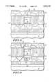
- FIG. 1Shown in FIG. 1, in cross-section, is a portion of a semiconductor substrate 10 having already undergone several process steps in accordance with the invention.
- the structure illustrated in FIG. 1includes a device layer 12 overlying substrate 10, and an insulating layer 14 overlying device layer 12.
- Device layer 12contains various device components commonly present in a semiconductor device, such as transistors, resistors, capacitors, and the like.
- the device componentsare fabricated in active device regions in substrate 10, which are electrically isolated by field isolation regions.
- the device componentsare comprised of patterned layers of semiconductor materials.
- the various device components of device layer 12contain contact regions enabling the various device components to be electrically contacted by an overlying metal interconnect layer.
- a first metal interconnect layer 16is separated from device layer 12 by insulating layer 14.
- Insulating layer 14can be any one of a number of common electrically insulating materials, such as chemical vapor deposited silicon dioxide, a silicate glass doped with either boron or phosphorous, or both, or a spin-on glass material, and the like.
- first interconnect layer 16is aluminum alloyed with copper.
- a first metal interconnect layerwill make contact to active components in device layer 12 through a series of contact openings (not shown) in insulating layer 14.
- the structure illustrated in FIG. 1is shown at a point in the process prior to the photolithographic patterning of first interconnect layer 16.
- first interconnect layer 16is covered by an anti-reflective coating 18.
- Anti-reflective coating 18reduces the optical reflection from interconnect layer 16 enabling high definition photolithographic patterning of first interconnect layer 16.
- an anti-reflective coatingis an optional processing feature, which can be eliminated depending upon the particular photolithographic patterning process.
- First metal interconnect layer 16contains a plurality of grain boundaries 19.
- the morphology of first metal interconnect layer 16is characterized by a plurality of metal grains.
- the average grain size of the metal filmdepends upon the particular process used to deposit the metal, and the processing parameters employed. For example, in a metal sputtering process, the grain size may be increased by increasing the substrate temperature during metal deposition.
- Metal interconnect layer 16is preferably formed by sputter deposition using a sputtering target containing aluminum and copper.
- Interlevel dielectric layer 20is photolithographically patterned, and both interlevel dielectric layer 20 and anti-reflective coating layer 18 are etched to form a via opening 22. Via opening 22 exposes a portion 23 of the surface of first metal interconnect layer 16.
- Interlevel dielectric layer 20can be any of a number of different electrically insulating materials, such as a silicate glass doped with either boron or phosphorous, or both, spin-on glass, silicon dioxide chemical vapor deposited using tetraethylorthosilane (TEOS) source gas, and the like.
- interlevel dielectric layer 20is anisotropically etched using fluorinated etching gases.
- interlevel dielectric layer 20is silicon dioxide; deposited by plasma enhanced chemical vapor deposition (PECVD) using tetraethylorthosilane (TEOS) source gas.
- PECVDplasma enhanced chemical vapor deposition
- TEOStetraethylorthosilane
- Interlevel dielectric layer 20is deposited to a thickness ranging from several hundred nanometers to more than 1 micron, and via opening 22 has a diameter of about 1 micrometer or less.
- a first copper interface layer 24is formed on exposed metal surface 23.
- Interface layer 24is preferably formed by a selective deposition process in which copper is preferentially chemical vapor deposited onto exposed metal surface 23.
- the deposition reactionis adjusted so that copper is deposited only on exposed interconnect metal.
- Exposed metal surfaces, such as surface 23,act as a nucleation site for the selective deposition process.
- the selectively deposited copperitself acts as a nucleation site so that the reaction continues depositing successive layers of copper, eventually forming a uniformly thick layer.
- the selectively deposited copperdoes not otherwise deposit on oxides or other dielectric materials.
- surface 23is cleaned using an RF sputtering process prior to beginning the selective deposition process.
- metal-organic-chemical-vapor-depositionMOCVD
- MOCVDmetal-organic-chemical-vapor-deposition
- the MOCVD processis carried out using metal-organic precursors of copper (I) and copper (II).
- the metal-organic copper precursorsare complex molecules in which organic ligands are bonded to copper through by an oxygen atom in the ligand.
- One family of metal-organic copper precursors for MOCVD copper depositionincludes copper (II) ⁇ -diketonate compounds.
- the copper ⁇ -diketonate compoundsare highly volatile and yield high purity copper at relatively low deposition temperatures.
- the copper depositionis carried out using the Cu(I) precursor, copper hexafluoroacetylacetonate vinyltrimethylsilane (Cu(hfac)VTMS).
- Cu(hfac)VTMScopper hexafluoroacetylacetonate vinyltrimethylsilane
- the Cu(hfac)VTMSis maintained in a liquid container at 40° C. and hydrogen is bubbled through the liquid.
- the hydrogen carrier gas flow rateis maintained at about 100-200 sccm, and most preferably at about 140 sccm.
- a small amount of water vaporis introduced to the precursor flow downstream from the liquid bubbler. The water vapor functions to increase the copper deposition rate at the susceptor.
- the addition of water vaporis an optional processing step which may be omitted when practicing the present invention.
- the water vaporis maintained at a partial pressure of about 5-15 millitorr, and most preferably at about 11 millitorr.
- the copperis preferably deposited in a cold wall deposition system having a susceptor, which is maintained at a temperature of about 190° C.
- a metal adhesion layer 26is deposited to overlie first interface layer 24 and interlevel dielectric layer 20.
- Adhesion layer 26provides an adhesive surface upon which a hard metal, such as a refractory metal, can be deposited.
- adhesion layer 26is a composite layer which includes a layer of titanium nitride overlying a layer of titanium.
- adhesion layer 26also functions as a diffusion barrier. The titanium nitride component of adhesion layer 26 will prevent components of reaction gasses used during a subsequent chemical vapor deposition steps from diffusing into first interface layer 24.
- adhesion layer 26can be another metal or metal alloy which has a low electrical resistance, such as a titanium-tungsten alloy, and the like.
- a refractory metalis blanket deposited to overlie adhesion layer 26, and both the refractory metal and the adhesive metal composite are etched to form a metal via plug 28, as illustrated in FIG. 4.
- via plug 28is tungsten.
- Tungstenis deposited by chemical vapor deposition using tungsten hexafluoride (WF 6 ) source gas.
- WF 6tungsten hexafluoride
- the titanium nitride in adhesion layer 26prevents the diffusion of fluorine into first interface layer 24.
- Adhesion layer 26also prevents tungsten nucleation on regions of first metal interconnect layer 16 adjacent to via opening 22.
- both the refractory metal and the adhesion metalare etched in a single etching tool using a sequential etching process.
- a fluorinated etch gasis used to etch away portions of the refractory metal overlying the upper surface of interlevel dielectric layer 20.
- the etching processis then continued to remove a portion of the refractory metal at the upper surface of via opening 22.
- the remaining exposed portions of adhesion layer 26are etched away using chlorinated etching gases.
- substrate 10can be removed from the etching tool, and the remaining exposed portions of adhesion layer 26 removed in a wet chemical etchant, or another plasma etching process.
- both the refractory metal and the adhesion metalcan be etched back using chemical-mechanical-polishing.
- the use of the flourinated etch gas used to etch away portions of the refractory metal overlying the upper surface of interlevel dielectric layer 20 followed by the use of chlorinated etch gas to remove the remaining exposed portions of adhesion layer 26 of the above embodimentmay not be required.
- the refractory metal etching processcreates a recessed region at the upper surface of via opening 22 in which a second copper interface layer 30 is formed.
- a previously described selective deposition processis carried out to form second interface layer 30.
- copperis selectively deposited to a thickness sufficient to fill the recess and form a smooth planar surface continuous with interlevel dielectric layer 20.
- a copper layercan be blanket deposited and planarized using a chemical-mechanical-polishing process.
- a copper permeable layer 31, such as titaniumcan be optionally deposited onto second interface layer 30 and interlevel dielectric layer 20.
- An additional titanium layercan improve the electromigration resistance of a metal interconnect by suppressing mass flux divergence internal to the metal interconnect itself.
- layer 31can be very thin, preferably, 10 to 20 nanometers. This is in contrast to the prior art where, typically, a refractory metal layer must be deposited to a great thickness (100 nanometers or more) to overcome low electrical resistivity characteristic of refractory metal barriers.
- the present inventionenables the use of a thin refractory metal layer, such as layer 31, to enhance electromigration resistance of an overlying interconnect layer, while avoiding the process complexity inherent in the deposition and processing of thick refractory layers.
- a second metal interconnect layer 32is formed to overlie interlevel dielectric layer 20 and second interface layer 30.
- Second metal interconnect layer 32is preferably a metal alloy similar to first metal interconnect layer 16.
- Second metal interconnect layer 32also contains grain boundaries 35 characteristic of the granular morphology of second metal interconnect layer 32.
- An optional anti-reflective coating 34overlies second metal interconnect layer 32.
- second metal interconnect layer 32Upon the formation of second metal interconnect layer 32, a multi-level metallization structure is complete.
- the structureincludes overlying metal interconnect layers 16 and 32, which are electrically coupled by a via plug 28. Copper interface layers 24 and 30 reside between the via plug and the interconnect metal and are confined within opening 22 created in interlevel dielectric layer 20. Interface layer 24 and 30 effectively separate the hard refractory metal body of via plug 28 from the soft, ductile metal of interconnect layers 16 and 32.
- first and second metal interconnect layer 16 and 32can be formed by one of a number of different aluminum alloys, such as aluminum titanium, aluminum scandium, aluminum palladium, and the like.
- an annealing processis carried out to form copper reservoirs 36 and 37 in the metal interconnect layers, as illustrated in FIG. 6.
- the annealing processis carried out in forming gas at a temperature of about 300°-500° C.
- the annealing processcauses copper to diffuse from interface layers 24 and 30 into adjacent regions of metal interconnect layers 16 and 32, respectively.
- the copper-rich reservoirsprovide a source of copper to replenish the copper that is depleted from the grain boundaries of the interconnect layers when electrical current is passed through the multi-level metal structure.
- the copper reservoirshave a copper concentration in the range of 1.5 to 5 weight percent.
- the copper concentration in copper reservoirs 36 and 37is substantially greater than that of interconnect layers 16 and 32, and is limited only by the capacity of the grain boundaries to adsorb copper under a given set of thermal annealing conditions.
- the copperfirst diffuses through layer 31, then into second metal interconnect layer 32. Because layer 32 is permeable to copper, the formation of copper reservoir 36 is not impeded by the presence of layer 32.
- the process of the inventionforms highly concentrated regions of copper at the specific locations in a multi-level metal structure where electron flux divergence is great.
- regions of high copper concentration in regions of high flux divergencethe electromigration of metal in the interconnects is prevented.
- electromigration in the interconnect metalis minimized, the current handling capability of the entire interconnect structure is increased.
- the greater current handling capability of the metal interconnect structure of the present inventionimproves the overall device performance. By providing high current levels at selected locations in a semiconductor device, electrical charge can be rapidly built up and dissipated, improving device performance parameters, such as capacitor charging, and transistor switching speeds, and the like.
- the present inventionavoids the necessity of depositing interconnect metal having high concentrations of copper, which is difficult to etch.
- High density aluminum interconnectsare typically etched in plasma etching systems using etching gases such as chlorine and boron trichloride. These gases readily react with copper causing extensive metal corrosion.
- etching gasessuch as chlorine and boron trichloride. These gases readily react with copper causing extensive metal corrosion.
- interconnect metalcan be deposited having copper concentrations of one weight percent or less.
Landscapes
- Physics & Mathematics (AREA)
- Condensed Matter Physics & Semiconductors (AREA)
- General Physics & Mathematics (AREA)
- Engineering & Computer Science (AREA)
- Computer Hardware Design (AREA)
- Microelectronics & Electronic Packaging (AREA)
- Power Engineering (AREA)
- Internal Circuitry In Semiconductor Integrated Circuit Devices (AREA)
Abstract
Description
Claims (12)
Priority Applications (1)
| Application Number | Priority Date | Filing Date | Title |
|---|---|---|---|
| US08/448,157US5527739A (en) | 1993-12-23 | 1995-05-23 | Process for fabricating a semiconductor device having an improved metal interconnect structure |
Applications Claiming Priority (2)
| Application Number | Priority Date | Filing Date | Title |
|---|---|---|---|
| US08/172,320US5442235A (en) | 1993-12-23 | 1993-12-23 | Semiconductor device having an improved metal interconnect structure |
| US08/448,157US5527739A (en) | 1993-12-23 | 1995-05-23 | Process for fabricating a semiconductor device having an improved metal interconnect structure |
Related Parent Applications (1)
| Application Number | Title | Priority Date | Filing Date |
|---|---|---|---|
| US08/172,320DivisionUS5442235A (en) | 1993-12-23 | 1993-12-23 | Semiconductor device having an improved metal interconnect structure |
Publications (1)
| Publication Number | Publication Date |
|---|---|
| US5527739Atrue US5527739A (en) | 1996-06-18 |
Family
ID=22627216
Family Applications (2)
| Application Number | Title | Priority Date | Filing Date |
|---|---|---|---|
| US08/172,320Expired - Fee RelatedUS5442235A (en) | 1993-12-23 | 1993-12-23 | Semiconductor device having an improved metal interconnect structure |
| US08/448,157Expired - Fee RelatedUS5527739A (en) | 1993-12-23 | 1995-05-23 | Process for fabricating a semiconductor device having an improved metal interconnect structure |
Family Applications Before (1)
| Application Number | Title | Priority Date | Filing Date |
|---|---|---|---|
| US08/172,320Expired - Fee RelatedUS5442235A (en) | 1993-12-23 | 1993-12-23 | Semiconductor device having an improved metal interconnect structure |
Country Status (1)
| Country | Link |
|---|---|
| US (2) | US5442235A (en) |
Cited By (49)
| Publication number | Priority date | Publication date | Assignee | Title |
|---|---|---|---|---|
| US5677244A (en)* | 1996-05-20 | 1997-10-14 | Motorola, Inc. | Method of alloying an interconnect structure with copper |
| US5681779A (en)* | 1994-02-04 | 1997-10-28 | Lsi Logic Corporation | Method of doping metal layers for electromigration resistance |
| US5714418A (en)* | 1995-11-08 | 1998-02-03 | Intel Corporation | Diffusion barrier for electrical interconnects in an integrated circuit |
| US5744192A (en)* | 1996-11-08 | 1998-04-28 | Sharp Microelectronics Technology, Inc. | Method of using water vapor to increase the conductivity of cooper desposited with cu(hfac)TMVS |
| US5770519A (en)* | 1995-06-05 | 1998-06-23 | Advanced Micro Devices, Inc. | Copper reservoir for reducing electromigration effects associated with a conductive via in a semiconductor device |
| US5804251A (en)* | 1995-12-29 | 1998-09-08 | Intel Corporation | Low temperature aluminum alloy plug technology |
| US5814557A (en)* | 1996-05-20 | 1998-09-29 | Motorola, Inc. | Method of forming an interconnect structure |
| US5907787A (en)* | 1995-02-13 | 1999-05-25 | Sony Corporation | Process for fabricating multilayer connection |
| US5939788A (en)* | 1998-03-11 | 1999-08-17 | Micron Technology, Inc. | Copper diffusion barrier, aluminum wetting layer and improved methods for filling openings in silicon substrates with cooper |
| US5953634A (en)* | 1995-02-13 | 1999-09-14 | Kabushiki Kaisha Toshiba | Method of manufacturing semiconductor device |
| US5970373A (en)* | 1996-05-10 | 1999-10-19 | Sharp Laboratories Of America, Inc. | Method for preventing oxidation in the formation of a via in an integrated circuit |
| US6001727A (en)* | 1996-04-01 | 1999-12-14 | Canon Kabushiki Kaisha | Method of making a semiconductor device |
| US6010749A (en)* | 1998-10-28 | 2000-01-04 | Goldman; Mark A. | Process for the production of volatile metal |
| US6025275A (en)* | 1996-12-19 | 2000-02-15 | Texas Instruments Incorporated | Method of forming improved thick plated copper interconnect and associated auxiliary metal interconnect |
| WO2000008230A1 (en)* | 1998-08-03 | 2000-02-17 | Advanced Technology Materials, Inc. | Copper precursor composition and process for manufacture of microelectronic device structures |
| US6030895A (en)* | 1995-01-03 | 2000-02-29 | International Business Machines Corporation | Method of making a soft metal conductor |
| US6100587A (en)* | 1999-08-26 | 2000-08-08 | Lucent Technologies Inc. | Silicon carbide barrier layers for porous low dielectric constant materials |
| US6110819A (en)* | 1994-10-31 | 2000-08-29 | International Business Machines Corporation | Interconnect structure using Al2 Cu for an integrated circuit chip |
| US6130161A (en)* | 1997-05-30 | 2000-10-10 | International Business Machines Corporation | Method of forming copper interconnections with enhanced electromigration resistance and reduced defect sensitivity |
| US6136670A (en)* | 1998-09-03 | 2000-10-24 | Micron Technology, Inc. | Semiconductor processing methods of forming contacts between electrically conductive materials |
| US6169024B1 (en) | 1998-09-30 | 2001-01-02 | Intel Corporation | Process to manufacture continuous metal interconnects |
| US6218303B1 (en)* | 1998-12-11 | 2001-04-17 | Vlsi Technology, Inc. | Via formation using oxide reduction of underlying copper |
| US6248665B1 (en) | 1999-07-06 | 2001-06-19 | Taiwan Semiconductor Manufacturing Company | Delamination improvement between Cu and dielectrics for damascene process |
| US6268280B1 (en)* | 1996-07-12 | 2001-07-31 | Kabushiki Kaisha Toshiba | Semiconductor device using dual damascene technology and method for manufacturing the same |
| US6287956B2 (en)* | 1997-04-25 | 2001-09-11 | Nec Corporation | Multilevel interconnecting structure in semiconductor device and method of forming the same |
| US6303480B1 (en)* | 1999-09-13 | 2001-10-16 | Applied Materials, Inc. | Silicon layer to improve plug filling by CVD |
| US6306732B1 (en)* | 1998-10-09 | 2001-10-23 | Advanced Micro Devices, Inc. | Method and apparatus for simultaneously improving the electromigration reliability and resistance of damascene vias using a controlled diffusivity barrier |
| US6331379B1 (en) | 1999-09-01 | 2001-12-18 | Micron Technology, Inc. | Photo-lithography process using multiple anti-reflective coatings |
| US6365514B1 (en) | 1997-12-23 | 2002-04-02 | Intel Corporation | Two chamber metal reflow process |
| US6380083B1 (en)* | 1998-08-28 | 2002-04-30 | Agere Systems Guardian Corp. | Process for semiconductor device fabrication having copper interconnects |
| US6395607B1 (en)* | 1999-06-09 | 2002-05-28 | Alliedsignal Inc. | Integrated circuit fabrication method for self-aligned copper diffusion barrier |
| US20020070419A1 (en)* | 2000-12-13 | 2002-06-13 | Farrar Paul A. | Method of forming buried conductor patterns by surface transformation of empty spaces in solid state materials |
| US20030087490A1 (en)* | 1998-07-07 | 2003-05-08 | Kazuhide Abe | Method for forming an interconnection in a semiconductor element |
| US6579795B1 (en)* | 2002-04-02 | 2003-06-17 | Intel Corporation | Method of making a semiconductor device that has copper damascene interconnects with enhanced electromigration reliability |
| US20030181018A1 (en)* | 2002-03-25 | 2003-09-25 | Micron Technology, Inc. | Low k interconnect dielectric using surface transformation |
| US20030178729A1 (en)* | 2002-03-25 | 2003-09-25 | Micron Technology, Inc. | Films deposited at glancing incidence for multilevel metallization |
| US20040003873A1 (en)* | 1999-03-05 | 2004-01-08 | Applied Materials, Inc. | Method and apparatus for annealing copper films |
| US6727172B1 (en) | 2002-06-12 | 2004-04-27 | Taiwan Semiconductor Manufacturing Company | Process to reduce chemical mechanical polishing damage of narrow copper lines |
| US20040079633A1 (en)* | 2000-07-05 | 2004-04-29 | Applied Materials, Inc. | Apparatus for electro chemical deposition of copper metallization with the capability of in-situ thermal annealing |
| US20040119154A1 (en)* | 2002-12-20 | 2004-06-24 | Michael Briere | Flip chip fet device |
| US20040125577A1 (en)* | 2002-12-27 | 2004-07-01 | Patrizio Vinciarelli | Low loss, high density array interconnection |
| US20040154185A1 (en)* | 1997-07-10 | 2004-08-12 | Applied Materials, Inc. | Method and apparatus for heating and cooling substrates |
| US20040209414A1 (en)* | 2003-04-18 | 2004-10-21 | Applied Materials, Inc. | Two position anneal chamber |
| US20050070036A1 (en)* | 2001-05-16 | 2005-03-31 | Geusic Joseph E. | Method of forming mirrors by surface transformation of empty spaces in solid state materials |
| US20050230262A1 (en)* | 2004-04-20 | 2005-10-20 | Semitool, Inc. | Electrochemical methods for the formation of protective features on metallized features |
| US20060138708A1 (en)* | 2002-01-17 | 2006-06-29 | Micron Technology, Inc. | Cellular materials formed using surface transformation |
| US20090014773A1 (en)* | 2007-07-10 | 2009-01-15 | Ching-Nan Hsiao | Two bit memory structure and method of making the same |
| US20110266674A1 (en)* | 2010-04-28 | 2011-11-03 | Taiwan Semiconductor Manufacturing Company, Ltd. | Laser Etch Via Formation |
| US9246085B1 (en)* | 2014-07-23 | 2016-01-26 | Intermolecular, Inc. | Shaping ReRAM conductive filaments by controlling grain-boundary density |
Families Citing this family (38)
| Publication number | Priority date | Publication date | Assignee | Title |
|---|---|---|---|---|
| JP3491237B2 (en)* | 1993-09-24 | 2004-01-26 | 日本テキサス・インスツルメンツ株式会社 | Stacked conductive film structure of semiconductor device |
| JP3104534B2 (en)* | 1994-06-27 | 2000-10-30 | ヤマハ株式会社 | Semiconductor device and its manufacturing method. |
| US5639691A (en)* | 1995-06-05 | 1997-06-17 | Advanced Micro Devices, Inc. | Copper pellet for reducing electromigration effects associated with a conductive via in a semiconductor device |
| US5633199A (en)* | 1995-11-02 | 1997-05-27 | Motorola Inc. | Process for fabricating a metallized interconnect structure in a semiconductor device |
| JP3304754B2 (en) | 1996-04-11 | 2002-07-22 | 三菱電機株式会社 | Multistage embedded wiring structure of integrated circuit |
| KR19980032463A (en)* | 1996-10-03 | 1998-07-25 | 윌리엄비.켐플러 | Via Pads and Caps for Improved Electromigration Capabilities |
| JPH10125865A (en)* | 1996-10-15 | 1998-05-15 | Fujitsu Ltd | Semiconductor device, semiconductor storage device, and method of manufacturing the same |
| US6037257A (en)* | 1997-05-08 | 2000-03-14 | Applied Materials, Inc. | Sputter deposition and annealing of copper alloy metallization |
| US5891802A (en)* | 1997-07-23 | 1999-04-06 | Advanced Micro Devices, Inc. | Method for fabricating a metallization stack structure to improve electromigration resistance and keep low resistivity of ULSI interconnects |
| US5981378A (en)* | 1997-07-25 | 1999-11-09 | Vlsi Technology, Inc. | Reliable interconnect via structures and methods for making the same |
| US6965165B2 (en) | 1998-12-21 | 2005-11-15 | Mou-Shiung Lin | Top layers of metal for high performance IC's |
| KR100351238B1 (en)* | 1999-09-14 | 2002-09-09 | 주식회사 하이닉스반도체 | Method of manufacturing a capacitor in a semiconductor device |
| TW490718B (en)* | 2000-01-25 | 2002-06-11 | Toshiba Corp | Semiconductor device and the manufacturing method thereof |
| US6943105B2 (en)* | 2002-01-18 | 2005-09-13 | International Business Machines Corporation | Soft metal conductor and method of making |
| US6930391B2 (en)* | 2002-08-27 | 2005-08-16 | Intel Corporation | Method for alloy-electroplating group IB metals with refractory metals for interconnections |
| JP2004319834A (en)* | 2003-04-17 | 2004-11-11 | Renesas Technology Corp | Semiconductor device and manufacturing method thereof |
| KR100653997B1 (en)* | 2005-04-26 | 2006-12-05 | 주식회사 하이닉스반도체 | Metal wiring of semiconductor device having low resistance and manufacturing method thereof |
| US7485968B2 (en) | 2005-08-11 | 2009-02-03 | Ziptronix, Inc. | 3D IC method and device |
| US7485540B2 (en)* | 2005-08-18 | 2009-02-03 | International Business Machines Corporation | Integrated BEOL thin film resistor |
| JP6225453B2 (en)* | 2012-05-24 | 2017-11-08 | 日亜化学工業株式会社 | Semiconductor device |
| US10886250B2 (en) | 2015-07-10 | 2021-01-05 | Invensas Corporation | Structures and methods for low temperature bonding using nanoparticles |
| US9953941B2 (en) | 2015-08-25 | 2018-04-24 | Invensas Bonding Technologies, Inc. | Conductive barrier direct hybrid bonding |
| TWI822659B (en) | 2016-10-27 | 2023-11-21 | 美商艾德亞半導體科技有限責任公司 | Structures and methods for low temperature bonding |
| US10515913B2 (en) | 2017-03-17 | 2019-12-24 | Invensas Bonding Technologies, Inc. | Multi-metal contact structure |
| US10446441B2 (en) | 2017-06-05 | 2019-10-15 | Invensas Corporation | Flat metal features for microelectronics applications |
| US10840205B2 (en) | 2017-09-24 | 2020-11-17 | Invensas Bonding Technologies, Inc. | Chemical mechanical polishing for hybrid bonding |
| US11056348B2 (en) | 2018-04-05 | 2021-07-06 | Invensas Bonding Technologies, Inc. | Bonding surfaces for microelectronics |
| US10790262B2 (en) | 2018-04-11 | 2020-09-29 | Invensas Bonding Technologies, Inc. | Low temperature bonded structures |
| US11244916B2 (en) | 2018-04-11 | 2022-02-08 | Invensas Bonding Technologies, Inc. | Low temperature bonded structures |
| US11393779B2 (en) | 2018-06-13 | 2022-07-19 | Invensas Bonding Technologies, Inc. | Large metal pads over TSV |
| KR20210009426A (en) | 2018-06-13 | 2021-01-26 | 인벤사스 본딩 테크놀로지스 인코포레이티드 | TV as a pad |
| US11011494B2 (en) | 2018-08-31 | 2021-05-18 | Invensas Bonding Technologies, Inc. | Layer structures for making direct metal-to-metal bonds at low temperatures in microelectronics |
| US11158573B2 (en) | 2018-10-22 | 2021-10-26 | Invensas Bonding Technologies, Inc. | Interconnect structures |
| US11244920B2 (en) | 2018-12-18 | 2022-02-08 | Invensas Bonding Technologies, Inc. | Method and structures for low temperature device bonding |
| WO2021236361A1 (en) | 2020-05-19 | 2021-11-25 | Invensas Bonding Technologies, Inc. | Laterally unconfined structure |
| US11264357B1 (en) | 2020-10-20 | 2022-03-01 | Invensas Corporation | Mixed exposure for large die |
| JP2024501017A (en) | 2020-12-28 | 2024-01-10 | アデイア セミコンダクター ボンディング テクノロジーズ インコーポレイテッド | Structure with through-substrate via and method for forming the same |
| JP2024501559A (en) | 2020-12-30 | 2024-01-12 | アデイア セミコンダクター ボンディング テクノロジーズ インコーポレイテッド | Structures with conductive features and methods of forming the same |
Citations (12)
| Publication number | Priority date | Publication date | Assignee | Title |
|---|---|---|---|---|
| US3743894A (en)* | 1972-06-01 | 1973-07-03 | Motorola Inc | Electromigration resistant semiconductor contacts and the method of producing same |
| JPS5561038A (en)* | 1978-10-31 | 1980-05-08 | Fujitsu Ltd | Manufacture of semiconductor device |
| US4335506A (en)* | 1980-08-04 | 1982-06-22 | International Business Machines Corporation | Method of forming aluminum/copper alloy conductors |
| JPS58110055A (en)* | 1981-12-23 | 1983-06-30 | Nec Corp | Semiconductor device |
| JPS58202551A (en)* | 1982-05-21 | 1983-11-25 | Hitachi Ltd | Wiring material of electro migration resistance |
| US4812419A (en)* | 1987-04-30 | 1989-03-14 | Hewlett-Packard Company | Via connection with thin resistivity layer |
| JPH0234929A (en)* | 1988-07-25 | 1990-02-05 | Matsushita Electron Corp | Manufacture of semiconductor device |
| JPH02206123A (en)* | 1989-02-06 | 1990-08-15 | Matsushita Electron Corp | Semiconductor device |
| JPH03255632A (en)* | 1990-03-05 | 1991-11-14 | Fujitsu Ltd | Semiconductor device and its manufacturing method |
| US5187300A (en)* | 1991-02-04 | 1993-02-16 | Air Products And Chemicals, Inc. | Volatile precursors for copper CVD |
| US5202579A (en)* | 1991-01-30 | 1993-04-13 | Mitsubishi Denki Kabushiki Kaisha | Semiconductor device having multilayer interconnection structure |
| US5284799A (en)* | 1991-03-27 | 1994-02-08 | Sony Corporation | Method of making a metal plug |
- 1993
- 1993-12-23USUS08/172,320patent/US5442235A/ennot_activeExpired - Fee Related
- 1995
- 1995-05-23USUS08/448,157patent/US5527739A/ennot_activeExpired - Fee Related
Patent Citations (12)
| Publication number | Priority date | Publication date | Assignee | Title |
|---|---|---|---|---|
| US3743894A (en)* | 1972-06-01 | 1973-07-03 | Motorola Inc | Electromigration resistant semiconductor contacts and the method of producing same |
| JPS5561038A (en)* | 1978-10-31 | 1980-05-08 | Fujitsu Ltd | Manufacture of semiconductor device |
| US4335506A (en)* | 1980-08-04 | 1982-06-22 | International Business Machines Corporation | Method of forming aluminum/copper alloy conductors |
| JPS58110055A (en)* | 1981-12-23 | 1983-06-30 | Nec Corp | Semiconductor device |
| JPS58202551A (en)* | 1982-05-21 | 1983-11-25 | Hitachi Ltd | Wiring material of electro migration resistance |
| US4812419A (en)* | 1987-04-30 | 1989-03-14 | Hewlett-Packard Company | Via connection with thin resistivity layer |
| JPH0234929A (en)* | 1988-07-25 | 1990-02-05 | Matsushita Electron Corp | Manufacture of semiconductor device |
| JPH02206123A (en)* | 1989-02-06 | 1990-08-15 | Matsushita Electron Corp | Semiconductor device |
| JPH03255632A (en)* | 1990-03-05 | 1991-11-14 | Fujitsu Ltd | Semiconductor device and its manufacturing method |
| US5202579A (en)* | 1991-01-30 | 1993-04-13 | Mitsubishi Denki Kabushiki Kaisha | Semiconductor device having multilayer interconnection structure |
| US5187300A (en)* | 1991-02-04 | 1993-02-16 | Air Products And Chemicals, Inc. | Volatile precursors for copper CVD |
| US5284799A (en)* | 1991-03-27 | 1994-02-08 | Sony Corporation | Method of making a metal plug |
Non-Patent Citations (10)
| Title |
|---|
| d Heurle et al., Metallization For Shallow Junction Silicon Technology, IBM Technical Disclosure Bulletin , vol. 19, No. 8, Jan. 1977, pp. 3232 3233.* |
| d'Heurle et al., "Metallization For Shallow Junction Silicon Technology, IBM Technical Disclosure Bulletin", vol. 19, No. 8, Jan. 1977, pp. 3232-3233. |
| Filippi, et al., 1992 VLSI multilevel Interconnect Conf., pp. 359 365.* |
| Filippi, et al., 1992 VLSI multilevel Interconnect Conf., pp. 359-365. |
| Hu et al., 1991 MRS Symposium Proceedings, 225, pp. 99 105, Electromigration in Al/W and Al(W)/w Interconnect Structures .* |
| Hu et al., 1991 MRS Symposium Proceedings, 225, pp. 99-105, "Electromigration in Al/W and Al(W)/w Interconnect Structures". |
| Tao, et al., 1992 IRPS Proceedings, pp. 338 343.* |
| Tao, et al., 1992 IRPS Proceedings, pp. 338-343. |
| Tao, et al., Proc. 1991 VLSI Multilevel Interconnect Conf., pp. 390 392, Electromigration Characteristics of Al/W via Contact Under Unidirectios .* |
| Tao, et al., Proc. 1991 VLSI Multilevel Interconnect Conf., pp. 390-392, "Electromigration Characteristics of Al/W via Contact Under Unidirectios". |
Cited By (84)
| Publication number | Priority date | Publication date | Assignee | Title |
|---|---|---|---|---|
| US5681779A (en)* | 1994-02-04 | 1997-10-28 | Lsi Logic Corporation | Method of doping metal layers for electromigration resistance |
| US6110819A (en)* | 1994-10-31 | 2000-08-29 | International Business Machines Corporation | Interconnect structure using Al2 Cu for an integrated circuit chip |
| US6030895A (en)* | 1995-01-03 | 2000-02-29 | International Business Machines Corporation | Method of making a soft metal conductor |
| US5907787A (en)* | 1995-02-13 | 1999-05-25 | Sony Corporation | Process for fabricating multilayer connection |
| US5953634A (en)* | 1995-02-13 | 1999-09-14 | Kabushiki Kaisha Toshiba | Method of manufacturing semiconductor device |
| US5770519A (en)* | 1995-06-05 | 1998-06-23 | Advanced Micro Devices, Inc. | Copper reservoir for reducing electromigration effects associated with a conductive via in a semiconductor device |
| US5714418A (en)* | 1995-11-08 | 1998-02-03 | Intel Corporation | Diffusion barrier for electrical interconnects in an integrated circuit |
| US5804251A (en)* | 1995-12-29 | 1998-09-08 | Intel Corporation | Low temperature aluminum alloy plug technology |
| US6001727A (en)* | 1996-04-01 | 1999-12-14 | Canon Kabushiki Kaisha | Method of making a semiconductor device |
| US5970373A (en)* | 1996-05-10 | 1999-10-19 | Sharp Laboratories Of America, Inc. | Method for preventing oxidation in the formation of a via in an integrated circuit |
| US5677244A (en)* | 1996-05-20 | 1997-10-14 | Motorola, Inc. | Method of alloying an interconnect structure with copper |
| US5814557A (en)* | 1996-05-20 | 1998-09-29 | Motorola, Inc. | Method of forming an interconnect structure |
| US6268280B1 (en)* | 1996-07-12 | 2001-07-31 | Kabushiki Kaisha Toshiba | Semiconductor device using dual damascene technology and method for manufacturing the same |
| US5744192A (en)* | 1996-11-08 | 1998-04-28 | Sharp Microelectronics Technology, Inc. | Method of using water vapor to increase the conductivity of cooper desposited with cu(hfac)TMVS |
| US6025275A (en)* | 1996-12-19 | 2000-02-15 | Texas Instruments Incorporated | Method of forming improved thick plated copper interconnect and associated auxiliary metal interconnect |
| US6287956B2 (en)* | 1997-04-25 | 2001-09-11 | Nec Corporation | Multilevel interconnecting structure in semiconductor device and method of forming the same |
| US6348731B1 (en) | 1997-05-30 | 2002-02-19 | International Business Machines Corporation | Copper interconnections with enhanced electromigration resistance and reduced defect sensitivity and method of forming same |
| US6287954B1 (en) | 1997-05-30 | 2001-09-11 | International Business Machines Corporation | Method of forming copper interconnections with enhanced electromigration resistance and reduced defect sensitivity |
| US6130161A (en)* | 1997-05-30 | 2000-10-10 | International Business Machines Corporation | Method of forming copper interconnections with enhanced electromigration resistance and reduced defect sensitivity |
| US20040154185A1 (en)* | 1997-07-10 | 2004-08-12 | Applied Materials, Inc. | Method and apparatus for heating and cooling substrates |
| US6929774B2 (en) | 1997-07-10 | 2005-08-16 | Applied Materials, Inc. | Method and apparatus for heating and cooling substrates |
| US6365514B1 (en) | 1997-12-23 | 2002-04-02 | Intel Corporation | Two chamber metal reflow process |
| US5939788A (en)* | 1998-03-11 | 1999-08-17 | Micron Technology, Inc. | Copper diffusion barrier, aluminum wetting layer and improved methods for filling openings in silicon substrates with cooper |
| US6204179B1 (en) | 1998-03-11 | 2001-03-20 | Micron Technology, Inc. | Copper diffusion barrier, aluminum wetting layer and improved methods for filling openings in silicon substrates with copper |
| US6903008B2 (en)* | 1998-07-07 | 2005-06-07 | Oki Electric Industry Co., Ltd. | Method for forming an interconnection in a semiconductor element |
| US20030087490A1 (en)* | 1998-07-07 | 2003-05-08 | Kazuhide Abe | Method for forming an interconnection in a semiconductor element |
| US6102993A (en)* | 1998-08-03 | 2000-08-15 | Advanced Technology Materials, Inc. | Copper precursor composition and process for manufacture of microelectronic device structures |
| WO2000008230A1 (en)* | 1998-08-03 | 2000-02-17 | Advanced Technology Materials, Inc. | Copper precursor composition and process for manufacture of microelectronic device structures |
| US6380083B1 (en)* | 1998-08-28 | 2002-04-30 | Agere Systems Guardian Corp. | Process for semiconductor device fabrication having copper interconnects |
| US6136670A (en)* | 1998-09-03 | 2000-10-24 | Micron Technology, Inc. | Semiconductor processing methods of forming contacts between electrically conductive materials |
| US7166922B1 (en) | 1998-09-30 | 2007-01-23 | Intel Corporation | Continuous metal interconnects |
| US6169024B1 (en) | 1998-09-30 | 2001-01-02 | Intel Corporation | Process to manufacture continuous metal interconnects |
| US6306732B1 (en)* | 1998-10-09 | 2001-10-23 | Advanced Micro Devices, Inc. | Method and apparatus for simultaneously improving the electromigration reliability and resistance of damascene vias using a controlled diffusivity barrier |
| US6010749A (en)* | 1998-10-28 | 2000-01-04 | Goldman; Mark A. | Process for the production of volatile metal |
| US6218303B1 (en)* | 1998-12-11 | 2001-04-17 | Vlsi Technology, Inc. | Via formation using oxide reduction of underlying copper |
| US20040003873A1 (en)* | 1999-03-05 | 2004-01-08 | Applied Materials, Inc. | Method and apparatus for annealing copper films |
| US7192494B2 (en) | 1999-03-05 | 2007-03-20 | Applied Materials, Inc. | Method and apparatus for annealing copper films |
| US6395607B1 (en)* | 1999-06-09 | 2002-05-28 | Alliedsignal Inc. | Integrated circuit fabrication method for self-aligned copper diffusion barrier |
| US6504247B2 (en) | 1999-06-09 | 2003-01-07 | Alliedsignal Inc. | Integrated having a self-aligned Cu diffusion barrier |
| US6248665B1 (en) | 1999-07-06 | 2001-06-19 | Taiwan Semiconductor Manufacturing Company | Delamination improvement between Cu and dielectrics for damascene process |
| US6410419B1 (en) | 1999-08-26 | 2002-06-25 | Agere Systems Guardian Corp. | Silicon carbide barrier layers for porous low dielectric constant materials |
| US6100587A (en)* | 1999-08-26 | 2000-08-08 | Lucent Technologies Inc. | Silicon carbide barrier layers for porous low dielectric constant materials |
| US20030155626A1 (en)* | 1999-09-01 | 2003-08-21 | Ireland Philip J. | Photolithography process using multiple anti-reflective coatings |
| US7387866B2 (en) | 1999-09-01 | 2008-06-17 | Micron Technology, Inc. | Photolithography process using multiple anti-reflective coatings |
| US6331379B1 (en) | 1999-09-01 | 2001-12-18 | Micron Technology, Inc. | Photo-lithography process using multiple anti-reflective coatings |
| US7250247B2 (en) | 1999-09-01 | 2007-07-31 | Micron Technology, Inc. | Photolithographic structures using multiple anti-reflecting coatings |
| US6303480B1 (en)* | 1999-09-13 | 2001-10-16 | Applied Materials, Inc. | Silicon layer to improve plug filling by CVD |
| US6602770B2 (en)* | 1999-09-13 | 2003-08-05 | Applied Materials, Inc. | Silicon layer to improve plug filling by CVD |
| US20040079633A1 (en)* | 2000-07-05 | 2004-04-29 | Applied Materials, Inc. | Apparatus for electro chemical deposition of copper metallization with the capability of in-situ thermal annealing |
| US7164188B2 (en) | 2000-12-13 | 2007-01-16 | Micron Technology, Inc. | Buried conductor patterns formed by surface transformation of empty spaces in solid state materials |
| US20020070419A1 (en)* | 2000-12-13 | 2002-06-13 | Farrar Paul A. | Method of forming buried conductor patterns by surface transformation of empty spaces in solid state materials |
| US20070036196A1 (en)* | 2001-05-16 | 2007-02-15 | Geusic Joseph E | Method of forming mirrors by surface transformation of empty spaces in solid state materials |
| US7260125B2 (en) | 2001-05-16 | 2007-08-21 | Micron Technology, Inc. | Method of forming mirrors by surface transformation of empty spaces in solid state materials |
| US7512170B2 (en) | 2001-05-16 | 2009-03-31 | Micron Technology, Inc. | Method of forming mirrors by surface transformation of empty spaces in solid state materials |
| US20050070036A1 (en)* | 2001-05-16 | 2005-03-31 | Geusic Joseph E. | Method of forming mirrors by surface transformation of empty spaces in solid state materials |
| US20050175058A1 (en)* | 2001-05-16 | 2005-08-11 | Geusic Joseph E. | Method of forming mirrors by surface transformation of empty spaces in solid state materials |
| US7142577B2 (en) | 2001-05-16 | 2006-11-28 | Micron Technology, Inc. | Method of forming mirrors by surface transformation of empty spaces in solid state materials and structures thereon |
| US7964124B2 (en) | 2002-01-17 | 2011-06-21 | Micron Technology, Inc. | Method of forming cellular material |
| US20060138708A1 (en)* | 2002-01-17 | 2006-06-29 | Micron Technology, Inc. | Cellular materials formed using surface transformation |
| US20030181018A1 (en)* | 2002-03-25 | 2003-09-25 | Micron Technology, Inc. | Low k interconnect dielectric using surface transformation |
| US7550824B2 (en) | 2002-03-25 | 2009-06-23 | Micron Technology, Inc. | Low k interconnect dielectric using surface transformation |
| US7485942B2 (en) | 2002-03-25 | 2009-02-03 | Micron Technology, Inc. | Films deposited at glancing incidence for multilevel metallization |
| US6777770B2 (en) | 2002-03-25 | 2004-08-17 | Micron Technology, Inc. | Films deposited at glancing incidence for multilevel metallization |
| US7109563B2 (en) | 2002-03-25 | 2006-09-19 | Micron Technology, Inc. | Films deposited at glancing incidence for multilevel metallization |
| US20060208335A1 (en)* | 2002-03-25 | 2006-09-21 | Micron Technology, Inc. | Films deposited at glancing incidence for multilevel metallization |
| US7132348B2 (en) | 2002-03-25 | 2006-11-07 | Micron Technology, Inc. | Low k interconnect dielectric using surface transformation |
| US20030178729A1 (en)* | 2002-03-25 | 2003-09-25 | Micron Technology, Inc. | Films deposited at glancing incidence for multilevel metallization |
| US20050029501A1 (en)* | 2002-03-25 | 2005-02-10 | Micron Technology, Inc. | Low k interconnect dielectric using surface transformation |
| US20040266220A1 (en)* | 2002-03-25 | 2004-12-30 | Micron Technology, Inc. | Films deposited at glancing incidence for multilevel metallization |
| US6579795B1 (en)* | 2002-04-02 | 2003-06-17 | Intel Corporation | Method of making a semiconductor device that has copper damascene interconnects with enhanced electromigration reliability |
| US6727172B1 (en) | 2002-06-12 | 2004-04-27 | Taiwan Semiconductor Manufacturing Company | Process to reduce chemical mechanical polishing damage of narrow copper lines |
| US7166898B2 (en) | 2002-12-20 | 2007-01-23 | Picor Corporation | Flip chip FET device |
| US6969909B2 (en) | 2002-12-20 | 2005-11-29 | Vlt, Inc. | Flip chip FET device |
| US20050269647A1 (en)* | 2002-12-20 | 2005-12-08 | Vlt Corporation, A Texas Corporation | Flip chip FET device |
| US20040119154A1 (en)* | 2002-12-20 | 2004-06-24 | Michael Briere | Flip chip fet device |
| US20040125577A1 (en)* | 2002-12-27 | 2004-07-01 | Patrizio Vinciarelli | Low loss, high density array interconnection |
| US7038917B2 (en) | 2002-12-27 | 2006-05-02 | Vlt, Inc. | Low loss, high density array interconnection |
| US7311810B2 (en) | 2003-04-18 | 2007-12-25 | Applied Materials, Inc. | Two position anneal chamber |
| US20040209414A1 (en)* | 2003-04-18 | 2004-10-21 | Applied Materials, Inc. | Two position anneal chamber |
| US20050230262A1 (en)* | 2004-04-20 | 2005-10-20 | Semitool, Inc. | Electrochemical methods for the formation of protective features on metallized features |
| US20090014773A1 (en)* | 2007-07-10 | 2009-01-15 | Ching-Nan Hsiao | Two bit memory structure and method of making the same |
| US20110266674A1 (en)* | 2010-04-28 | 2011-11-03 | Taiwan Semiconductor Manufacturing Company, Ltd. | Laser Etch Via Formation |
| US8519538B2 (en)* | 2010-04-28 | 2013-08-27 | Taiwan Semiconductor Manufacturing Company, Ltd. | Laser etch via formation |
| US9246085B1 (en)* | 2014-07-23 | 2016-01-26 | Intermolecular, Inc. | Shaping ReRAM conductive filaments by controlling grain-boundary density |
Also Published As
| Publication number | Publication date |
|---|---|
| US5442235A (en) | 1995-08-15 |
Similar Documents
| Publication | Publication Date | Title |
|---|---|---|
| US5527739A (en) | Process for fabricating a semiconductor device having an improved metal interconnect structure | |
| US5391517A (en) | Process for forming copper interconnect structure | |
| US6133147A (en) | Process for selective metal deposition in holes of semiconductor device | |
| US5677244A (en) | Method of alloying an interconnect structure with copper | |
| US5989623A (en) | Dual damascene metallization | |
| US5447887A (en) | Method for capping copper in semiconductor devices | |
| US6541374B1 (en) | Method of depositing a diffusion barrier for copper interconnection applications | |
| JP2828540B2 (en) | Method for forming low resistance and low defect density tungsten contacts for silicon semiconductor wafers | |
| KR100623556B1 (en) | Interconnection structure and fabrication process therefor | |
| US6955983B2 (en) | Methods of forming metal interconnections of semiconductor devices by treating a barrier metal layer | |
| US20020024142A1 (en) | Semiconductor device and manufacturing method of the same | |
| US6054382A (en) | Method of improving texture of metal films in semiconductor integrated circuits | |
| US6110828A (en) | In-situ capped aluminum plug (CAP) process using selective CVD AL for integrated plug/interconnect metallization | |
| US6576543B2 (en) | Method for selectively depositing diffusion barriers | |
| JPH0548935B2 (en) | ||
| US5994775A (en) | Metal-filled via/contact opening with thin barrier layers in integrated circuit structure for fast response, and process for making same | |
| US5223455A (en) | Method of forming refractory metal film | |
| US6043149A (en) | Method of purifying a metal line in a semiconductor device | |
| US6723645B2 (en) | Method of forming a metal wiring in a semiconductor device | |
| JPH0922907A (en) | Method for forming embedded conductive layer | |
| KR100289515B1 (en) | Barrier emtal layer and method of forming the same | |
| US5948705A (en) | Method of forming interconnection line | |
| JP3149912B2 (en) | Semiconductor device and method of manufacturing the same | |
| KR100250455B1 (en) | Method of manufacturing metal line of semiconductor device using copper thin film | |
| US7169706B2 (en) | Method of using an adhesion precursor layer for chemical vapor deposition (CVD) copper deposition |
Legal Events
| Date | Code | Title | Description |
|---|---|---|---|
| REMI | Maintenance fee reminder mailed | ||
| FPAY | Fee payment | Year of fee payment:4 | |
| SULP | Surcharge for late payment | ||
| FPAY | Fee payment | Year of fee payment:8 | |
| AS | Assignment | Owner name:FREESCALE SEMICONDUCTOR, INC., TEXAS Free format text:ASSIGNMENT OF ASSIGNORS INTEREST;ASSIGNOR:MOTOROLA, INC.;REEL/FRAME:015698/0657 Effective date:20040404 Owner name:FREESCALE SEMICONDUCTOR, INC.,TEXAS Free format text:ASSIGNMENT OF ASSIGNORS INTEREST;ASSIGNOR:MOTOROLA, INC.;REEL/FRAME:015698/0657 Effective date:20040404 | |
| AS | Assignment | Owner name:CITIBANK, N.A. AS COLLATERAL AGENT, NEW YORK Free format text:SECURITY AGREEMENT;ASSIGNORS:FREESCALE SEMICONDUCTOR, INC.;FREESCALE ACQUISITION CORPORATION;FREESCALE ACQUISITION HOLDINGS CORP.;AND OTHERS;REEL/FRAME:018855/0129 Effective date:20061201 Owner name:CITIBANK, N.A. AS COLLATERAL AGENT,NEW YORK Free format text:SECURITY AGREEMENT;ASSIGNORS:FREESCALE SEMICONDUCTOR, INC.;FREESCALE ACQUISITION CORPORATION;FREESCALE ACQUISITION HOLDINGS CORP.;AND OTHERS;REEL/FRAME:018855/0129 Effective date:20061201 | |
| REMI | Maintenance fee reminder mailed | ||
| LAPS | Lapse for failure to pay maintenance fees | ||
| STCH | Information on status: patent discontinuation | Free format text:PATENT EXPIRED DUE TO NONPAYMENT OF MAINTENANCE FEES UNDER 37 CFR 1.362 | |
| FP | Expired due to failure to pay maintenance fee | Effective date:20080618 | |
| AS | Assignment | Owner name:FREESCALE SEMICONDUCTOR, INC., TEXAS Free format text:PATENT RELEASE;ASSIGNOR:CITIBANK, N.A., AS COLLATERAL AGENT;REEL/FRAME:037354/0225 Effective date:20151207 |