US5527423A - Chemical mechanical polishing slurry for metal layers - Google Patents
Chemical mechanical polishing slurry for metal layersDownload PDFInfo
- Publication number
- US5527423A US5527423AUS08/319,213US31921394AUS5527423AUS 5527423 AUS5527423 AUS 5527423AUS 31921394 AUS31921394 AUS 31921394AUS 5527423 AUS5527423 AUS 5527423A
- Authority
- US
- United States
- Prior art keywords
- slurry
- particles
- alumina
- less
- polishing
- Prior art date
- Legal status (The legal status is an assumption and is not a legal conclusion. Google has not performed a legal analysis and makes no representation as to the accuracy of the status listed.)
- Expired - Lifetime
Links
- 239000002002slurrySubstances0.000titleclaimsabstractdescription127
- 238000005498polishingMethods0.000titleclaimsabstractdescription89
- 229910052751metalInorganic materials0.000titleclaimsabstractdescription25
- 239000002184metalSubstances0.000titleclaimsabstractdescription25
- 239000000126substanceSubstances0.000titleclaimsdescription21
- 239000002245particleSubstances0.000claimsabstractdescription84
- 239000012736aqueous mediumSubstances0.000claimsabstractdescription12
- PNEYBMLMFCGWSK-UHFFFAOYSA-Naluminium oxideInorganic materials[O-2].[O-2].[O-2].[Al+3].[Al+3]PNEYBMLMFCGWSK-UHFFFAOYSA-N0.000claimsdescription44
- 238000000034methodMethods0.000claimsdescription39
- 230000001590oxidative effectEffects0.000claimsdescription29
- 239000004094surface-active agentSubstances0.000claimsdescription21
- WFKWXMTUELFFGS-UHFFFAOYSA-NtungstenChemical compound[W]WFKWXMTUELFFGS-UHFFFAOYSA-N0.000claimsdescription19
- 229910052721tungstenInorganic materials0.000claimsdescription19
- 239000010937tungstenSubstances0.000claimsdescription19
- 239000000203mixtureSubstances0.000claimsdescription17
- 238000009826distributionMethods0.000claimsdescription15
- 239000004065semiconductorSubstances0.000claimsdescription11
- -1siloxanesChemical class0.000claimsdescription9
- 239000000654additiveSubstances0.000claimsdescription7
- 238000005411Van der Waals forceMethods0.000claimsdescription6
- 229910052782aluminiumInorganic materials0.000claimsdescription6
- XAGFODPZIPBFFR-UHFFFAOYSA-NaluminiumChemical compound[Al]XAGFODPZIPBFFR-UHFFFAOYSA-N0.000claimsdescription6
- 239000000758substrateSubstances0.000claimsdescription6
- 230000000996additive effectEffects0.000claimsdescription5
- 150000003839saltsChemical class0.000claimsdescription5
- RTAQQCXQSZGOHL-UHFFFAOYSA-NTitaniumChemical compound[Ti]RTAQQCXQSZGOHL-UHFFFAOYSA-N0.000claimsdescription4
- 229920001577copolymerPolymers0.000claimsdescription4
- 239000010936titaniumSubstances0.000claimsdescription4
- 229910052719titaniumInorganic materials0.000claimsdescription4
- XTEGARKTQYYJKE-UHFFFAOYSA-MChlorateChemical class[O-]Cl(=O)=OXTEGARKTQYYJKE-UHFFFAOYSA-M0.000claimsdescription3
- RYGMFSIKBFXOCR-UHFFFAOYSA-NCopperChemical compound[Cu]RYGMFSIKBFXOCR-UHFFFAOYSA-N0.000claimsdescription3
- AZDRQVAHHNSJOQ-UHFFFAOYSA-NalumaneChemical class[AlH3]AZDRQVAHHNSJOQ-UHFFFAOYSA-N0.000claimsdescription3
- 150000003863ammonium saltsChemical class0.000claimsdescription3
- 239000010949copperSubstances0.000claimsdescription3
- 229910052802copperInorganic materials0.000claimsdescription3
- 159000000014iron saltsChemical class0.000claimsdescription3
- VLTRZXGMWDSKGL-UHFFFAOYSA-Nperchloric acidChemical classOCl(=O)(=O)=OVLTRZXGMWDSKGL-UHFFFAOYSA-N0.000claimsdescription3
- 150000002978peroxidesChemical class0.000claimsdescription3
- JRKICGRDRMAZLK-UHFFFAOYSA-Lpersulfate groupChemical groupS(=O)(=O)([O-])OOS(=O)(=O)[O-]JRKICGRDRMAZLK-UHFFFAOYSA-L0.000claimsdescription3
- 150000004714phosphonium saltsChemical class0.000claimsdescription3
- 159000000001potassium saltsChemical class0.000claimsdescription3
- 150000003242quaternary ammonium saltsChemical class0.000claimsdescription3
- 159000000000sodium saltsChemical class0.000claimsdescription3
- NRTOMJZYCJJWKI-UHFFFAOYSA-NTitanium nitrideChemical compound[Ti]#NNRTOMJZYCJJWKI-UHFFFAOYSA-N0.000claimsdescription2
- 238000000354decomposition reactionMethods0.000claimsdescription2
- MAKDTFFYCIMFQP-UHFFFAOYSA-Ntitanium tungstenChemical compound[Ti].[W]MAKDTFFYCIMFQP-UHFFFAOYSA-N0.000claimsdescription2
- 239000002280amphoteric surfactantSubstances0.000claims3
- 239000003945anionic surfactantSubstances0.000claims3
- 239000003093cationic surfactantSubstances0.000claims3
- 150000002170ethersChemical class0.000claims3
- 239000002736nonionic surfactantSubstances0.000claims3
- 150000004696coordination complexChemical class0.000claims2
- 239000000956alloySubstances0.000claims1
- 229910045601alloyInorganic materials0.000claims1
- MVFCKEFYUDZOCX-UHFFFAOYSA-Niron(2+);dinitrateChemical group[Fe+2].[O-][N+]([O-])=O.[O-][N+]([O-])=OMVFCKEFYUDZOCX-UHFFFAOYSA-N0.000claims1
- 150000004706metal oxidesChemical class0.000abstractdescription35
- 229910001111Fine metalInorganic materials0.000abstractdescription8
- 235000012431wafersNutrition0.000description29
- 229910044991metal oxideInorganic materials0.000description27
- VYPSYNLAJGMNEJ-UHFFFAOYSA-NSilicium dioxideChemical compoundO=[Si]=OVYPSYNLAJGMNEJ-UHFFFAOYSA-N0.000description20
- VCJMYUPGQJHHFU-UHFFFAOYSA-Niron(3+);trinitrateChemical compound[Fe+3].[O-][N+]([O-])=O.[O-][N+]([O-])=O.[O-][N+]([O-])=OVCJMYUPGQJHHFU-UHFFFAOYSA-N0.000description14
- 238000011068loading methodMethods0.000description11
- XLYOFNOQVPJJNP-UHFFFAOYSA-NwaterSubstancesOXLYOFNOQVPJJNP-UHFFFAOYSA-N0.000description11
- 230000000694effectsEffects0.000description10
- 239000008367deionised waterSubstances0.000description9
- 229910021641deionized waterInorganic materials0.000description9
- 239000007787solidSubstances0.000description8
- 230000008569processEffects0.000description7
- 238000003917TEM imageMethods0.000description6
- 230000007547defectEffects0.000description6
- 238000004519manufacturing processMethods0.000description6
- 239000000377silicon dioxideSubstances0.000description6
- 229910021485fumed silicaInorganic materials0.000description5
- 239000011164primary particleSubstances0.000description5
- 239000003082abrasive agentSubstances0.000description3
- 239000002585baseSubstances0.000description3
- 239000000356contaminantSubstances0.000description3
- 238000007796conventional methodMethods0.000description3
- 239000012535impuritySubstances0.000description3
- 238000009413insulationMethods0.000description3
- 239000007788liquidSubstances0.000description3
- 239000000463materialSubstances0.000description3
- 238000005259measurementMethods0.000description3
- 239000013049sedimentSubstances0.000description3
- 230000006641stabilisationEffects0.000description3
- 238000011105stabilizationMethods0.000description3
- 229910018404Al2 O3Inorganic materials0.000description2
- IJGRMHOSHXDMSA-UHFFFAOYSA-NAtomic nitrogenChemical compoundN#NIJGRMHOSHXDMSA-UHFFFAOYSA-N0.000description2
- RTZKZFJDLAIYFH-UHFFFAOYSA-NDiethyl etherChemical compoundCCOCCRTZKZFJDLAIYFH-UHFFFAOYSA-N0.000description2
- MHAJPDPJQMAIIY-UHFFFAOYSA-NHydrogen peroxideChemical compoundOOMHAJPDPJQMAIIY-UHFFFAOYSA-N0.000description2
- GWEVSGVZZGPLCZ-UHFFFAOYSA-NTitan oxideChemical compoundO=[Ti]=OGWEVSGVZZGPLCZ-UHFFFAOYSA-N0.000description2
- 238000005299abrasionMethods0.000description2
- VSCWAEJMTAWNJL-UHFFFAOYSA-Kaluminium trichlorideChemical compoundCl[Al](Cl)ClVSCWAEJMTAWNJL-UHFFFAOYSA-K0.000description2
- 238000004458analytical methodMethods0.000description2
- 230000015572biosynthetic processEffects0.000description2
- 238000001246colloidal dispersionMethods0.000description2
- 239000006185dispersionSubstances0.000description2
- 239000003995emulsifying agentSubstances0.000description2
- 238000005189flocculationMethods0.000description2
- 230000016615flocculationEffects0.000description2
- YBMRDBCBODYGJE-UHFFFAOYSA-Ngermanium dioxideChemical compoundO=[Ge]=OYBMRDBCBODYGJE-UHFFFAOYSA-N0.000description2
- 238000010191image analysisMethods0.000description2
- 239000002609mediumSubstances0.000description2
- QGLKJKCYBOYXKC-UHFFFAOYSA-NnonaoxidotritungstenChemical compoundO=[W]1(=O)O[W](=O)(=O)O[W](=O)(=O)O1QGLKJKCYBOYXKC-UHFFFAOYSA-N0.000description2
- 238000012545processingMethods0.000description2
- 238000006748scratchingMethods0.000description2
- 230000002393scratching effectEffects0.000description2
- 238000012876topographyMethods0.000description2
- 229910001930tungsten oxideInorganic materials0.000description2
- VXEGSRKPIUDPQT-UHFFFAOYSA-N4-[4-(4-methoxyphenyl)piperazin-1-yl]anilineChemical compoundC1=CC(OC)=CC=C1N1CCN(C=2C=CC(N)=CC=2)CC1VXEGSRKPIUDPQT-UHFFFAOYSA-N0.000description1
- JBRZTFJDHDCESZ-UHFFFAOYSA-NAsGaChemical compound[As]#[Ga]JBRZTFJDHDCESZ-UHFFFAOYSA-N0.000description1
- KCXVZYZYPLLWCC-UHFFFAOYSA-NEDTAChemical compoundOC(=O)CN(CC(O)=O)CCN(CC(O)=O)CC(O)=OKCXVZYZYPLLWCC-UHFFFAOYSA-N0.000description1
- 229910001218Gallium arsenideInorganic materials0.000description1
- 229910003944H3 PO4Inorganic materials0.000description1
- UFHFLCQGNIYNRP-UHFFFAOYSA-NHydrogenChemical compound[H][H]UFHFLCQGNIYNRP-UHFFFAOYSA-N0.000description1
- 239000005708Sodium hypochloriteSubstances0.000description1
- 239000002253acidSubstances0.000description1
- 239000003929acidic solutionSubstances0.000description1
- 230000002378acidificating effectEffects0.000description1
- 150000007513acidsChemical class0.000description1
- 230000004075alterationEffects0.000description1
- QVGXLLKOCUKJST-UHFFFAOYSA-Natomic oxygenChemical compound[O]QVGXLLKOCUKJST-UHFFFAOYSA-N0.000description1
- 239000003637basic solutionSubstances0.000description1
- 239000007844bleaching agentSubstances0.000description1
- CETPSERCERDGAM-UHFFFAOYSA-Nceric oxideChemical compoundO=[Ce]=OCETPSERCERDGAM-UHFFFAOYSA-N0.000description1
- 229910000422cerium(IV) oxideInorganic materials0.000description1
- 239000007795chemical reaction productSubstances0.000description1
- 239000003795chemical substances by applicationSubstances0.000description1
- 150000001860citric acid derivativesChemical class0.000description1
- 238000004140cleaningMethods0.000description1
- 239000000701coagulantSubstances0.000description1
- 230000015271coagulationEffects0.000description1
- 238000005345coagulationMethods0.000description1
- 239000008119colloidal silicaSubstances0.000description1
- 239000000084colloidal systemSubstances0.000description1
- 238000002485combustion reactionMethods0.000description1
- 230000000052comparative effectEffects0.000description1
- 238000001816coolingMethods0.000description1
- 230000003247decreasing effectEffects0.000description1
- 230000001419dependent effectEffects0.000description1
- 239000003599detergentSubstances0.000description1
- 230000004069differentiationEffects0.000description1
- 239000004205dimethyl polysiloxaneSubstances0.000description1
- 235000013870dimethyl polysiloxaneNutrition0.000description1
- 239000002270dispersing agentSubstances0.000description1
- 239000000428dustSubstances0.000description1
- 238000001962electrophoresisMethods0.000description1
- 238000005516engineering processMethods0.000description1
- 238000005187foamingMethods0.000description1
- 230000036571hydrationEffects0.000description1
- 238000006703hydration reactionMethods0.000description1
- 239000001257hydrogenSubstances0.000description1
- 229910052739hydrogenInorganic materials0.000description1
- 230000007062hydrolysisEffects0.000description1
- 238000006460hydrolysis reactionMethods0.000description1
- 230000006872improvementEffects0.000description1
- 230000001788irregularEffects0.000description1
- 230000002427irreversible effectEffects0.000description1
- 238000007521mechanical polishing techniqueMethods0.000description1
- 150000002739metalsChemical class0.000description1
- 238000002156mixingMethods0.000description1
- 238000012986modificationMethods0.000description1
- 230000004048modificationEffects0.000description1
- 150000002823nitratesChemical class0.000description1
- 229910052757nitrogenInorganic materials0.000description1
- 239000007800oxidant agentSubstances0.000description1
- 230000003647oxidationEffects0.000description1
- 238000007254oxidation reactionMethods0.000description1
- TWNQGVIAIRXVLR-UHFFFAOYSA-Noxo(oxoalumanyloxy)alumaneChemical compoundO=[Al]O[Al]=OTWNQGVIAIRXVLR-UHFFFAOYSA-N0.000description1
- 239000001301oxygenSubstances0.000description1
- 229910052760oxygenInorganic materials0.000description1
- 238000000059patterningMethods0.000description1
- 238000000206photolithographyMethods0.000description1
- 238000007517polishing processMethods0.000description1
- 229920000435poly(dimethylsiloxane)Polymers0.000description1
- 239000002994raw materialSubstances0.000description1
- 229920006395saturated elastomerPolymers0.000description1
- 229910052710siliconInorganic materials0.000description1
- 239000010703siliconSubstances0.000description1
- 239000005049silicon tetrachlorideSubstances0.000description1
- SUKJFIGYRHOWBL-UHFFFAOYSA-Nsodium hypochloriteChemical compound[Na+].Cl[O-]SUKJFIGYRHOWBL-UHFFFAOYSA-N0.000description1
- 239000000243solutionSubstances0.000description1
- 238000001179sorption measurementMethods0.000description1
- 239000003381stabilizerSubstances0.000description1
- 150000003467sulfuric acid derivativesChemical class0.000description1
- 238000004627transmission electron microscopyMethods0.000description1
- 239000000080wetting agentSubstances0.000description1
- 239000002023woodSubstances0.000description1
Images


Classifications
- B—PERFORMING OPERATIONS; TRANSPORTING
- B24—GRINDING; POLISHING
- B24D—TOOLS FOR GRINDING, BUFFING OR SHARPENING
- B24D3/00—Physical features of abrasive bodies, or sheets, e.g. abrasive surfaces of special nature; Abrasive bodies or sheets characterised by their constituents
- C—CHEMISTRY; METALLURGY
- C23—COATING METALLIC MATERIAL; COATING MATERIAL WITH METALLIC MATERIAL; CHEMICAL SURFACE TREATMENT; DIFFUSION TREATMENT OF METALLIC MATERIAL; COATING BY VACUUM EVAPORATION, BY SPUTTERING, BY ION IMPLANTATION OR BY CHEMICAL VAPOUR DEPOSITION, IN GENERAL; INHIBITING CORROSION OF METALLIC MATERIAL OR INCRUSTATION IN GENERAL
- C23F—NON-MECHANICAL REMOVAL OF METALLIC MATERIAL FROM SURFACE; INHIBITING CORROSION OF METALLIC MATERIAL OR INCRUSTATION IN GENERAL; MULTI-STEP PROCESSES FOR SURFACE TREATMENT OF METALLIC MATERIAL INVOLVING AT LEAST ONE PROCESS PROVIDED FOR IN CLASS C23 AND AT LEAST ONE PROCESS COVERED BY SUBCLASS C21D OR C22F OR CLASS C25
- C23F3/00—Brightening metals by chemical means
- C—CHEMISTRY; METALLURGY
- C09—DYES; PAINTS; POLISHES; NATURAL RESINS; ADHESIVES; COMPOSITIONS NOT OTHERWISE PROVIDED FOR; APPLICATIONS OF MATERIALS NOT OTHERWISE PROVIDED FOR
- C09G—POLISHING COMPOSITIONS; SKI WAXES
- C09G1/00—Polishing compositions
- C09G1/02—Polishing compositions containing abrasives or grinding agents
- C—CHEMISTRY; METALLURGY
- C09—DYES; PAINTS; POLISHES; NATURAL RESINS; ADHESIVES; COMPOSITIONS NOT OTHERWISE PROVIDED FOR; APPLICATIONS OF MATERIALS NOT OTHERWISE PROVIDED FOR
- C09K—MATERIALS FOR MISCELLANEOUS APPLICATIONS, NOT PROVIDED FOR ELSEWHERE
- C09K3/00—Materials not provided for elsewhere
- C09K3/14—Anti-slip materials; Abrasives
- C09K3/1436—Composite particles, e.g. coated particles
- C—CHEMISTRY; METALLURGY
- C09—DYES; PAINTS; POLISHES; NATURAL RESINS; ADHESIVES; COMPOSITIONS NOT OTHERWISE PROVIDED FOR; APPLICATIONS OF MATERIALS NOT OTHERWISE PROVIDED FOR
- C09K—MATERIALS FOR MISCELLANEOUS APPLICATIONS, NOT PROVIDED FOR ELSEWHERE
- C09K3/00—Materials not provided for elsewhere
- C09K3/14—Anti-slip materials; Abrasives
- C09K3/1454—Abrasive powders, suspensions and pastes for polishing
- C09K3/1463—Aqueous liquid suspensions
- H—ELECTRICITY
- H01—ELECTRIC ELEMENTS
- H01L—SEMICONDUCTOR DEVICES NOT COVERED BY CLASS H10
- H01L21/00—Processes or apparatus adapted for the manufacture or treatment of semiconductor or solid state devices or of parts thereof
- H01L21/02—Manufacture or treatment of semiconductor devices or of parts thereof
- H01L21/04—Manufacture or treatment of semiconductor devices or of parts thereof the devices having potential barriers, e.g. a PN junction, depletion layer or carrier concentration layer
- H01L21/18—Manufacture or treatment of semiconductor devices or of parts thereof the devices having potential barriers, e.g. a PN junction, depletion layer or carrier concentration layer the devices having semiconductor bodies comprising elements of Group IV of the Periodic Table or AIIIBV compounds with or without impurities, e.g. doping materials
- H01L21/30—Treatment of semiconductor bodies using processes or apparatus not provided for in groups H01L21/20 - H01L21/26
- H01L21/31—Treatment of semiconductor bodies using processes or apparatus not provided for in groups H01L21/20 - H01L21/26 to form insulating layers thereon, e.g. for masking or by using photolithographic techniques; After treatment of these layers; Selection of materials for these layers
- H01L21/3205—Deposition of non-insulating-, e.g. conductive- or resistive-, layers on insulating layers; After-treatment of these layers
- H01L21/321—After treatment
- H01L21/32115—Planarisation
- H01L21/3212—Planarisation by chemical mechanical polishing [CMP]
Definitions
- the present inventionrelates to a chemical mechanical polishing slurry for semiconductor device planarization and, more particularly, to a chemical mechanical polishing slurry for use on polishing metal layers.
- a semiconductor wafertypically includes a substrate, such as such as a silicon or gallium arsenide wafer, on which a plurality of integrated circuits have been formed. Integrated circuits are chemically and physically integrated into a substrate by patterning regions in the substrate and layers on the substrate. The layers are generally formed of various materials having either a conductive, insulating or semiconducting nature. In order for a device to have high yields, it is crucial to start with a flat semiconductor wafer and, as a result, it is often necessary to polish a side or part of a semiconductor wafer. If the process steps of device fabrication are performed on a wafer surface that is not uniform, various problems can occur which may results in a large number of inoperable devices.
- CMPchemical mechanical polishing
- Typical polishing slurries available for CMP oxide processescontain an abrasive material such as silica or alumina in an acidic or basic solution.
- an abrasive materialsuch as silica or alumina in an acidic or basic solution.
- U.S. Pat. No. 5,245,790 to Jerbicdescribes a technique for chemical mechanical polishing of semiconductor wafers using ultrasonic energy and a silica based slurry in a KOH solution.
- U.S. Pat. No. 5,244,534 to Yu et al.discloses a method of forming conductive plugs within an insulation layer. The process results in a plug of material, such as tungsten, which is more even with the insulation layer surface than that achieved using conventional plug formation techniques.
- abrasive particlessuch as Al 2 O 3 and etchants such as H 2 O 2 and either KOH or NH 4 OH are used in the first CMP step to remove the tungsten at a predictable rate while removing very little of the insulation.
- the second CMP steputilizes a slurry consisting of an abrasive material, such as aluminum oxide, and an oxidizing component of hydrogen peroxide and water.
- U.S. Pat. No. 5,209,816 to Yu et al.teaches a CMP slurry comprising H 3 PO 4 , H 2 O 2 , H 2 O and a solid abrasive material while U.S. Pat. Nos.
- the present inventionis directed to a chemical mechanical polishing slurry for polishing metal layers of semiconductor devices comprising high purity, fine metal oxide particles uniformly dispersed in a stable aqueous medium.
- the particleshave a surface area ranging from about 40 m 2 /g to about 430 m 2 /g, an aggregate size distribution less than about 1.0 micron, a mean aggregate diameter less than about 0.4 micron and a force sufficient to repel and overcome the van der Waals forces between the particles.
- the metal oxide particlesalso have a maximum zeta potential greater than about ⁇ 10 millivolts. Also disclosed is a method of polishing tungsten layers with the polishing slurry of the present invention.
- FIG. 1is a transmission electron micrograph (TEM) showing metal oxide particles of fumed alumina of the present invention at 50,000 ⁇ magnification.
- TEMtransmission electron micrograph
- FIG. 2is an aggregate size distribution for metal oxide particles of fumed alumina for use in the polishing slurry of the present invention.
- FIG. 3is an aggregate size distribution for metal oxide particles of fumed silica for use in the polishing slurry of the present invention.
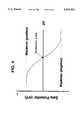
- FIG. 4illustrates a theoretical plot of pH on the x-axis versus zeta potential in millivolts on the y-axis.
- FIG. 5illustrates the effect of the particle composition on tungsten polishing rate and selectivity to thermal oxide for a series of wafers utilizing the polishing slurry of the present invention.
- the x-axisindicates the wafer number and the y-axis indicates the polishing rate of tungsten in ⁇ /minute.
- FIG. 6illustrates the effect on particle morphology, phase and solids content on tungsten polishing rate for a series of wafers utilizing the polishing slurry of the present invention.
- the x-axisindicates the wafer number and the y-axis indicates the polishing rate of tungsten in ⁇ /minute.
- FIG. 7illustrates the polishing rate of aluminum and selectivity to thermal oxide for a series of wafers utilizing the polishing slurry of the present invention.
- the x-axisindicates the wafer number and the y-axis indicates the polishing rate of aluminum in ⁇ /minute.
- FIG. 8illustrates the influence that aggregate size distribution and zeta potential has on colloidal stability by plotting the amount of sediment as a function of time.
- the present inventionis directed to a chemical mechanical polishing slurry comprising high purity, fine metal oxide particles uniformly dispersed in an aqueous medium.
- the particles of the present inventiondiffer from the "abrasive particles" of the prior art by having a surface area ranging from about 40 m 2 /g to about 430 m 2 /g, an aggregate size distribution less than about 1.0 micron, a mean aggregate diameter less than about 0.4 micron and a force sufficient to repel and overcome the van der Waals forces between the particles.
- FIG. 1is a TEM (transmission electron micrograph) for metal oxide particles of fumed alumina in the slurry of the present invention.
- the surface area of the particlestypically ranges from about 40 m 2 /g to about 430 m 2 /g.
- the particlesmay comprise between 0.5% and 55% of the slurry depending on the degree of abrasion required.
- the abrasion of the metal oxide particlesis a function of the particle composition, the degree of crystallinity and the crystalline phase, e.g. gamma or alpha for alumina.
- the optimum surface area and loading levelwill vary depending upon which fine metal oxide particles are chosen for a particular polishing slurry, as well as the degree of crystallinity and phase of the particles.
- solid loadings of less than 12% by weight for alumina particles having surface areas ranging from about 70 m 2 /g to about 170 m 2 /gis preferred.
- solid loadings of less than 7%is preferred for alumina particles.
- the metal oxide particles of the present inventionare of a high purity and have an aggregate size distribution of less than about 1.0 micron in order to avoid scratching, pit marks, divots and other surface imperfections during the polishing.
- FIGS. 2 and 3illustrate aggregate size distributions for metal oxide particles of the present invention for fumed alumina and silica, respectively.
- High puritymeans that the total impurity content is typically less than 1% and preferably less than 0.01% (i.e. 100 ppm).
- Sources of impuritiestypically include raw material impurities and trace processing contaminants.
- the aggregate size of the particlesrefers to the measurement of the branched, three dimensional chains of fused primary particles (individual molten spheres).
- TEMtransmission electron microscopy
- the metal oxide particle sampleis dispersed in a liquid medium until the agglomerates have been reversed to aggregates. Its concentration is then adjusted until discrete aggregates are shown on the TEM grid.
- Multiple fields on the gridare then imaged using an image analysis system manufactured by Kontron Instruments (Everett, Mass.) and stored on a video tape until greater than 1000 aggregates are imaged and stored.
- the stored imagesare in turn fed into an image analysis computer with a frame-grabber board for further processing, i.e. cleaning up aberrations, adjusting background and normalizing the image.
- Individual aggregates in the binary fieldare measured for a number of particle parameters, i.e. aggregate size, using known techniques such as that described in ASTM D3849-89. Measurements may be recalled individually or in the form of statistical or histogram distributions.
- the aggregates of the metal oxide particlesare uniformly dispersed in a stable aqueous medium.
- uniformly dispersedis meant that the aggregates are isolated and well distributed throughout the medium.
- stableis typically meant that the aggregates will not re-agglomerate and settle out (e.g. form a hard, dense sediment).
- the aggregateswill remain stable for at least a three month period of time.
- the metal oxides particles of the present inventionin addition to having an aggregate size distribution less that 1.0 micron, have an average or mean aggregate diameter of less than about 0.4 micron and that the particles of the present invention have a force sufficient to repel and overcome the van der Waals attractive forces between the particles.
- the mean aggregate diameterrefers to the average equivalent spherical diameter when using TEM image analysis, i.e. based on the cross-sectional area of the aggregate.
- forceis meant that either the surface potential or the hydration force of the metal oxide particles must be sufficient to repel and overcome the van der Waals attractive forces between the particles.
- the metal oxide particleswill have a mean aggregate size distribution less than 0.3 micron and also have a maximum zeta potential greater than ⁇ 10 millivolts.
- Zeta potential ( ⁇ )is the potential difference, measured in a liquid, between the shear plane and the bulk of the liquid beyond the limits of the electrical double layer. The zeta potential is dependent on the pH of the aqueous medium as illustrated in FIG. 4.
- the isoelectric pointis defined as the pH at which zeta potential is zero. As the pH is increased or decreased away from the isoelectric point, the surface charge is increased negatively or positively, respectively.
- the surface chargewill reach an asymptote, the asymptote being referred to as the maximum zeta potential.
- the maximum zeta potential and isoelectric pointare functions of the metal oxide composition and that the maximum zeta potential can be effected by the addition of salts to the aqueous medium.
- zeta potentialsplease see R. J. Hunter, Zeta Potential in Colloid Science (Academic Press 1981).
- the zeta potentialcannot be measured directly, the zeta potential can be measured by a variety of known techniques, such as electrophoresis, electrokinetic sonic amplitude, and analytical techniques including ultrasonic vibration potential.
- the zeta potential referred towas determined by measurement of the electrokinetic sonic amplitude using the Matec MBS-8000 instrument (available from Matec Applied Sciences, Inc., Hopkington, Mass.).
- an oxidizing componentmay be added to the polishing slurry to oxidize the metal layer to its corresponding oxide.
- an oxidizing componentis used to oxidize a metal layer to its corresponding oxide, such as tungsten to tungsten oxide.
- the layeris mechanically polished to remove the tungsten oxide from the layer.
- oxidizing componentsinclude oxidizing metal salts, oxidizing metal complexes, iron salts such as nitrates, sulfates, EDTA, citrates, potassium ferricyanide and the like, aluminum salts, sodium salts, potassium salts, ammonium salts, quaternary ammonium salts, phosphonium salts, peroxides, chlorates, perchlorates, permanganates, persulfates and mixtures thereof.
- the oxidizing componentis present in the slurry in an amount sufficient to ensure rapid oxidation of the metal layer while balancing the mechanical and chemical polishing components of the slurry.
- oxidizing componentsare typically present in the slurry from about 0.5% to 15% by weight, and preferably in a range between 1% and 7% by weight.
- a variety of additivessuch as surfactants, polymeric stabilizers or other surface active dispersing agents, can be used.
- surfactantssuch as surfactants, polymeric stabilizers or other surface active dispersing agents.
- suitable surfactants for use in the present inventionare disclosed in, for example, Kirk-Othmer, Encyclopedia of Chemical Technology, 3rd Edition, Vol.
- a surfactantconsisting of a copolymer of polydimethyl siloxane and polyoxyalkylene ether was found to be suitable.
- the amount of an additive used, such as a surfactant, in the present inventionshould be sufficient to achieve effective steric stabilization of the slurry and will typically vary depending on the particular surfactant selected and the nature of the surface of the metal oxide particle. For example, if not enough of a selected surfactant is used, it will have little or no effect on stabilization. On the other hand, too much of the surfactant may result in undesirable foaming and/or flocculation in the slurry. As a result, additives like surfactants should generally be present in a range between about 0.001% and 10% by weight.
- the additivemay be added directly to the slurry or treated onto the surface of the metal oxide particle utilizing known techniques. In either case, the amount of additive is adjusted to achieve the desired concentration in the polishing slurry.
- the metal oxide particles of the present inventionare typically precipitated aluminas, fumed silicas or fumed aluminas and preferably are fumed silicas or fumed aluminas.
- the production of fumed silicas and aluminasis a well-documented process which involves the hydrolysis of suitable feedstock vapor, such as silicon tetrachloride or aluminum chloride, in a flame of hydrogen and oxygen.
- suitable feedstock vaporsuch as silicon tetrachloride or aluminum chloride
- Molten particles of roughly spherical shapesare formed in the combustion process, the diameters of which are varied through process parameters.
- These molten spheres of fumed silica or aluminatypically referred to as primary particles, fuse with one another by undergoing collisions at their contact points to form branched, three dimensional chain-like aggregates.
- the precipitated metal oxide particlesmay be manufactured utilizing conventional techniques and are typically formed by the coagulation of the desired particles from an aqueous medium under the influence of high salt concentrations, acids or other coagulants.
- the particlesare filtered, washed, dried and separated from residues of other reaction products by conventional techniques known to those skilled in the art.
- the polishing slurry of the present inventionmay be used as a one package system (metal oxide particles and oxidizing component, if desired, in a stable aqueous medium) or two package system (the first package consists of the metal oxide particles in a stable aqueous medium and the second package consists of oxidizing component) with any standard polishing equipment appropriate for use on the desired metal layer of the wafer.
- the two package systemis used when an oxidizing component decomposes or hydrolyses in the presence of certain metal oxide particles over time.
- the oxidizing componentmay be added to the slurry just prior to polishing.
- the polishing slurry of the present inventionhas been found useful in providing effective polishing to metal layers at desired polishing rates while minimizing surface imperfections and defects.
- Non-limiting illustrations of the polishing slurry of the present inventionfollow.
- the polishing slurrieswere prepared.
- the first slurryconsisted of 3 weight percent fumed alumina, 5 weight percent ferric nitrate and the remainder deionized water.
- the second slurryconsisted of 3 weight percent fumed silica, 5 weight percent ferric nitrate and the remainder deionized water. Further properties of both slurries are described in Table I.
- the two slurrieswere utilized to chemically-mechanically polish a tungsten layer having a thickness of approximately 7500 ⁇ .
- the polishing conditions and performance resultsare illustrated in Table II.
- both polishing slurries of the present inventionwere effective in achieving acceptable polishing rates and wafer surfaces of a high quality.
- the composition of the metal oxide particle and its phasehave an impact on the polishing rate of the tungsten layer and on selectivity (i.e. the polishing rate ratio between tungsten and thermal oxide).
- the particular metal oxide chosen for polishing a layer of tungstenmay depend on the desired selectivity and polishing rate.
- a conventional slurrywas prepared consisting of 8 weight percent of a commercial alumina, 5 weight percent ferric nitrate and the remainder deionized water.
- the slurrywas utilized to chemically mechanically polish a tungsten layer having a thickness of approximately 7500 ⁇ .
- the slurry of commercial aluminaremoved 750 ⁇ /min and produced wafers of a poor quality.
- the polishing rate obtained by the slurry of commercial aluminawas unacceptable for most polishing applications.
- polishing slurrieswere prepared to investigate the effect of particle morphology and solids content on the polishing performance for a fumed alumina slurry.
- the first, second and third slurrieswhich consisted of 8 weight percent fumed alumina, 5 weight percent ferric nitrate and the remainder deionized water, were prepared to examine the effect of particle morphology and crystallinity under aggressive polishing conditions, i.e. high pressure, high table speed, high solids loading.
- the fourth and fifth slurrieswhich consisted of 3 weight percent fumed alumina, 5 weight percent ferric nitrate and the remainder deionized water, were prepared to examine the effect of particle morphology and crystallinity under less aggressive polishing conditions, i.e.
- phase and morphologyi.e. surface area
- selectivityi.e. the polishing rate ratio between tungsten and thermal oxide
- surface qualitya less dramatic effect on polishing rate
- the phase and morphologyhave a significant effect on polishing rate and surface quality.
- high quality waferswere produced by polishing with slurries 3 (at 8% loading), 4 (at 3% loading) and 5 (at 3% loading).
- a polishing slurrywas prepared consisting of 8 percent fumed silica, 5 weight percent ferric nitrate and the remainder deionized water. Further properties of the slurry are described in Table V. The slurry was utilized to chemically-mechanically polish an aluminum layer having a thickness of approximately 7500 ⁇ . The polishing conditions and performance results are illustrated in Table VI.
- the polishing slurry of the present inventionis effective in achieving an acceptable polishing rate for an aluminum layer and wafers with high surface quality.
- the first slurryconsisted of 8 weight percent fumed alumina as described in the present invention, 5 weight percent ferric nitrate and the remainder deionized water.
- the second slurryconsisted of 8 weight percent of a commercially available precipitated alumina sold under the name Ultralox M100. Further properties of the slurries are listed in Table VII.
- FIG. 8illustrates the amount of metal oxide particles in the respective slurries which settled over a twenty-four hour period.
- the particleswere measured using a Dynometer instrument manufactured by Byk Gardner, Inc. As noted, no settling was detected in slurry 1 of the present invention.
- slurry 2 of commercially available aluminashowed a continuous build-up in sediment over the twenty-four hour period. At the end of the period, the bulk of the alumina had settled out to form a dense hard cake. When used at this time without additional steps to redisperse the cake and stabilize the slurry, slurry 2 achieved low polishing rates and produced significant scratching on the wafer, thus yielding a wafer of poor quality.
- the polishing slurry of the present inventionhas been found particularly useful in chemical mechanical planarization to remove uneven topography, layers of material, surface defects including scratches, roughness, or contaminant particles such as dirt or dust.
- semiconductor processes utilizing this slurryexperience an improvement in surface quality, device reliability and yield as compared to conventional etch back techniques.
- the fine metal oxide particleshave been directed to aluminas and silicas, it is understood that the teachings herein have applicability to other fine metal oxide particles such as germania, ceria, titania and the like.
- the metal oxide particlesmay be utilized to polish other metal surfaces such as copper and titanium, as well as underlayers such as titanium, titanium nitride and titanium tungsten.
Landscapes
- Chemical & Material Sciences (AREA)
- Engineering & Computer Science (AREA)
- Organic Chemistry (AREA)
- Materials Engineering (AREA)
- Mechanical Engineering (AREA)
- General Physics & Mathematics (AREA)
- Computer Hardware Design (AREA)
- Metallurgy (AREA)
- Physics & Mathematics (AREA)
- Condensed Matter Physics & Semiconductors (AREA)
- Chemical Kinetics & Catalysis (AREA)
- Manufacturing & Machinery (AREA)
- General Chemical & Material Sciences (AREA)
- Microelectronics & Electronic Packaging (AREA)
- Power Engineering (AREA)
- Composite Materials (AREA)
- Mechanical Treatment Of Semiconductor (AREA)
- Polishing Bodies And Polishing Tools (AREA)
- Finish Polishing, Edge Sharpening, And Grinding By Specific Grinding Devices (AREA)
- ing And Chemical Polishing (AREA)
Abstract
Description
TABLE I ______________________________________ Aggregate Max. Zeta Slurry Surface Area Diameter Potential Base (m.sup.2 /g) (nm) (mV) Phase ______________________________________ Fumed 55 86 >+30 80% gamma Alumina Fumed 90 109 >+12 Amorphous Silica ______________________________________
TABLE II __________________________________________________________________________Slurry Pressure Flow Rate Table Spindle Polishing Base (psi) (ml/min) Speed (rpm) Speed (rpm) (Å/min) Selectivity* Quality __________________________________________________________________________Fumed 5 200 50 50 3000 110:1 High Alumina Fumed 5 200 50 50 2000 10:1 High Silica __________________________________________________________________________ (*Thermal Oxide; High = Less than 10 defects/wafer)
TABLE III ______________________________________ Aggregate Max. Zeta Surface Area Diameter Potential Slurry (m.sup.2 /g) (nm) (mV) Phase ______________________________________ 1 55 86 ˜+20-35 80% gamma 2 85 88 >+30 40% gamma 3 100 87 >+20 20% gamma 4 55 86 >+30 80% gamma 5 100 87 >+20 20% gamma ______________________________________
TABLE IV __________________________________________________________________________ Pressure Flow Rate Table Spindle Polishing Slurry (psi) (ml/min) Speed (rpm) Speed (rpm) (Å/min) Selectivity* Quality __________________________________________________________________________1 9 200 100 25 4850 50:1Low 2 9 200 100 25 3900 110:1Low 3 9 200 100 25 3700NA High 4 6 200 50 50 3100NA High 5 6 200 50 50 600 NA High __________________________________________________________________________ (*Thermal Oxide; High = Less than 10 defects/wafer; Low = Greater than 100 defect/wafer.)
TABLE V ______________________________________ Aggregate Max. Zeta Particle Surface Area Diameter Potential Comp. (m.sup.2 /g) (nm) (mV) Phase ______________________________________ Fumed 90 109 ˜+12 Amorphous Silica ______________________________________
TABLE VI __________________________________________________________________________ Pressure Flow Rate Table Spindle Polishing Slurry (psi) (ml/min) Speed (rpm) Speed (rpm) (Å/min) Selectivity* Quality __________________________________________________________________________Fumed 9 200 50 25 2932 80:1 High Silica __________________________________________________________________________ (*Thermal Oxide; High = Less than 10 defects/wafer)
TABLE VII ______________________________________ Surface Area Mean Aggregate Max. Zeta Slurry (m.sup.2 /g) Diameter (nm) Potential (mV) ______________________________________ 1 55 94.3 +32 2NA 450 +10 ______________________________________
Claims (39)
Priority Applications (14)
| Application Number | Priority Date | Filing Date | Title |
|---|---|---|---|
| US08/319,213US5527423A (en) | 1994-10-06 | 1994-10-06 | Chemical mechanical polishing slurry for metal layers |
| AU35494/95AAU3549495A (en) | 1994-10-06 | 1995-09-01 | Chemical mechanical polishing slurry for metal layers |
| PCT/US1995/011424WO1996011082A1 (en) | 1994-10-06 | 1995-09-01 | Chemical mechanical polishing slurry for metal layers |
| CN95196473ACN1074035C (en) | 1994-10-06 | 1995-09-01 | Chemical mechanical polishing slurry for metal layers |
| HK98103979.2AHK1004666B (en) | 1994-10-06 | 1995-09-01 | Chemical mechanical polishing slurry for metal layers |
| MYPI95002712AMY112735A (en) | 1994-10-06 | 1995-09-13 | Chemical mechanical polishing slurry for metal layers |
| IL11545495AIL115454A (en) | 1994-10-06 | 1995-09-28 | Chemical-mechanical polishing slurry for metal layers and method for polishing same |
| ES95306994TES2159495T3 (en) | 1994-10-06 | 1995-10-03 | WATER SPOOL SUSPENSION FOR CHEMICAL-MECHANICAL POLISHING OF METAL LAYERS. |
| DE69527406TDE69527406T2 (en) | 1994-10-06 | 1995-10-03 | Suspension for mixture-mechanical polishing of metal layers |
| AT95306994TATE220711T1 (en) | 1994-10-06 | 1995-10-03 | SUSPENSION FOR MIXTURE MECHANICAL POLISHING OF METAL LAYERS |
| DE0708160TDE708160T1 (en) | 1994-10-06 | 1995-10-03 | Suspension for mixture-mechanical polishing of metal layers |
| EP95306994AEP0708160B1 (en) | 1994-10-06 | 1995-10-03 | Chemical mechanical polishing slurry for metal layers |
| JP25887595AJP3377892B2 (en) | 1994-10-06 | 1995-10-05 | Chemical / mechanical polishing slurry for metal layer |
| KR1019950034358AKR100362141B1 (en) | 1994-10-06 | 1995-10-06 | Chemical mechanical metal polishing method and polishing slurry |
Applications Claiming Priority (1)
| Application Number | Priority Date | Filing Date | Title |
|---|---|---|---|
| US08/319,213US5527423A (en) | 1994-10-06 | 1994-10-06 | Chemical mechanical polishing slurry for metal layers |
Publications (1)
| Publication Number | Publication Date |
|---|---|
| US5527423Atrue US5527423A (en) | 1996-06-18 |
Family
ID=23241322
Family Applications (1)
| Application Number | Title | Priority Date | Filing Date |
|---|---|---|---|
| US08/319,213Expired - LifetimeUS5527423A (en) | 1994-10-06 | 1994-10-06 | Chemical mechanical polishing slurry for metal layers |
Country Status (12)
| Country | Link |
|---|---|
| US (1) | US5527423A (en) |
| EP (1) | EP0708160B1 (en) |
| JP (1) | JP3377892B2 (en) |
| KR (1) | KR100362141B1 (en) |
| CN (1) | CN1074035C (en) |
| AT (1) | ATE220711T1 (en) |
| AU (1) | AU3549495A (en) |
| DE (2) | DE708160T1 (en) |
| ES (1) | ES2159495T3 (en) |
| IL (1) | IL115454A (en) |
| MY (1) | MY112735A (en) |
| WO (1) | WO1996011082A1 (en) |
Cited By (478)
| Publication number | Priority date | Publication date | Assignee | Title |
|---|---|---|---|---|
| WO1997013889A1 (en)* | 1995-10-10 | 1997-04-17 | Rodel, Inc. | Improved polishing slurries and methods for their use |
| US5647952A (en)* | 1996-04-01 | 1997-07-15 | Industrial Technology Research Institute | Chemical/mechanical polish (CMP) endpoint method |
| WO1997043087A1 (en)* | 1996-05-10 | 1997-11-20 | Cabot Corporation | Chemical mechanical polishing slurry for metal layers and films |
| WO1997047030A1 (en)* | 1996-06-06 | 1997-12-11 | Cabot Corporation | Fluoride additive containing chemical mechanical polishing slurry and method for use of same |
| US5700383A (en)* | 1995-12-21 | 1997-12-23 | Intel Corporation | Slurries and methods for chemical mechanical polish of aluminum and titanium aluminide |
| WO1998004646A1 (en)* | 1996-07-25 | 1998-02-05 | Ekc Technology, Inc. | Chemical mechanical polishing composition and process |
| US5726099A (en)* | 1995-11-07 | 1998-03-10 | International Business Machines Corporation | Method of chemically mechanically polishing an electronic component using a non-selective ammonium persulfate slurry |
| US5728308A (en)* | 1995-05-26 | 1998-03-17 | Sony Corporation | Method of polishing a semiconductor substrate during production of a semiconductor device |
| US5731245A (en)* | 1994-08-05 | 1998-03-24 | International Business Machines Corp. | High aspect ratio low resistivity lines/vias with a tungsten-germanium alloy hard cap |
| US5735963A (en)* | 1996-12-17 | 1998-04-07 | Lucent Technologies Inc. | Method of polishing |
| US5752875A (en)* | 1995-12-14 | 1998-05-19 | International Business Machines Corporation | Method of chemically-mechanically polishing an electronic component |
| WO1998023697A1 (en)* | 1996-11-26 | 1998-06-04 | Cabot Corporation | Composition and method for polishing rigid disks |
| WO1998023408A1 (en)* | 1996-11-26 | 1998-06-04 | Cabot Corporation | A composition and slurry useful for metal cmp |
| US5773364A (en)* | 1996-10-21 | 1998-06-30 | Motorola, Inc. | Method for using ammonium salt slurries for chemical mechanical polishing (CMP) |
| US5783489A (en)* | 1996-09-24 | 1998-07-21 | Cabot Corporation | Multi-oxidizer slurry for chemical mechanical polishing |
| US5804513A (en)* | 1996-08-29 | 1998-09-08 | Sumitomo Chemical Company, Ltd. | Abrasive composition and use of the same |
| US5840629A (en)* | 1995-12-14 | 1998-11-24 | Sematech, Inc. | Copper chemical mechanical polishing slurry utilizing a chromate oxidant |
| US5846398A (en)* | 1996-08-23 | 1998-12-08 | Sematech, Inc. | CMP slurry measurement and control technique |
| US5863838A (en)* | 1996-07-22 | 1999-01-26 | Motorola, Inc. | Method for chemically-mechanically polishing a metal layer |
| US5866031A (en)* | 1996-06-19 | 1999-02-02 | Sematech, Inc. | Slurry formulation for chemical mechanical polishing of metals |
| US5895550A (en)* | 1996-12-16 | 1999-04-20 | Micron Technology, Inc. | Ultrasonic processing of chemical mechanical polishing slurries |
| US5897375A (en)* | 1997-10-20 | 1999-04-27 | Motorola, Inc. | Chemical mechanical polishing (CMP) slurry for copper and method of use in integrated circuit manufacture |
| US5904159A (en)* | 1995-11-10 | 1999-05-18 | Tokuyama Corporation | Polishing slurries and a process for the production thereof |
| WO1999027581A1 (en)* | 1997-11-20 | 1999-06-03 | Advanced Technology Materials, Inc. | CHEMICAL MECHANICAL POLISHING OF FeRAM CAPACITORS |
| US5916855A (en)* | 1997-03-26 | 1999-06-29 | Advanced Micro Devices, Inc. | Chemical-mechanical polishing slurry formulation and method for tungsten and titanium thin films |
| US5928962A (en)* | 1998-06-01 | 1999-07-27 | Motorola, Inc. | Process for forming a semiconductor device |
| US5954997A (en)* | 1996-12-09 | 1999-09-21 | Cabot Corporation | Chemical mechanical polishing slurry useful for copper substrates |
| US5958288A (en)* | 1996-11-26 | 1999-09-28 | Cabot Corporation | Composition and slurry useful for metal CMP |
| US5985748A (en)* | 1997-12-01 | 1999-11-16 | Motorola, Inc. | Method of making a semiconductor device using chemical-mechanical polishing having a combination-step process |
| US6001269A (en)* | 1997-05-20 | 1999-12-14 | Rodel, Inc. | Method for polishing a composite comprising an insulator, a metal, and titanium |
| US6008123A (en)* | 1997-11-04 | 1999-12-28 | Lucent Technologies Inc. | Method for using a hardmask to form an opening in a semiconductor substrate |
| US6017463A (en)* | 1997-11-21 | 2000-01-25 | Advanced Micro Devices, Inc. | Point of use mixing for LI/plug tungsten polishing slurry to improve existing slurry |
| US6022807A (en)* | 1996-04-24 | 2000-02-08 | Micro Processing Technology, Inc. | Method for fabricating an integrated circuit |
| US6027554A (en)* | 1996-01-29 | 2000-02-22 | Fujimi Incorporated | Polishing composition |
| WO2000010920A1 (en)* | 1998-08-19 | 2000-03-02 | Nanogram Corporation | Aluminum oxide particles |
| US6033596A (en)* | 1996-09-24 | 2000-03-07 | Cabot Corporation | Multi-oxidizer slurry for chemical mechanical polishing |
| US6037260A (en)* | 1998-02-20 | 2000-03-14 | Industrial Technology Research Institute | Polishing composition |
| US6039891A (en)* | 1996-09-24 | 2000-03-21 | Cabot Corporation | Multi-oxidizer precursor for chemical mechanical polishing |
| US6043159A (en)* | 1996-10-23 | 2000-03-28 | Clariant Chimie S.A. | Chemical mechanical polishing process for layers of isolating materials based on silicon derivatives or silicon |
| US6046110A (en)* | 1995-06-08 | 2000-04-04 | Kabushiki Kaisha Toshiba | Copper-based metal polishing solution and method for manufacturing a semiconductor device |
| WO2000023534A1 (en)* | 1998-10-21 | 2000-04-27 | W.R. Grace & Co.-Conn. | Slurries of abrasive inorganic oxide particles and method for adjusting the abrasiveness of the particles |
| WO2000024842A1 (en) | 1998-10-23 | 2000-05-04 | Arch Specialty Chemicals, Inc. | A chemical mechanical polishing slurry system having an activator solution |
| US6063306A (en)* | 1998-06-26 | 2000-05-16 | Cabot Corporation | Chemical mechanical polishing slurry useful for copper/tantalum substrate |
| US6083838A (en)* | 1998-05-20 | 2000-07-04 | Lucent Technologies Inc. | Method of planarizing a surface on a semiconductor wafer |
| US6093649A (en)* | 1998-08-07 | 2000-07-25 | Rodel Holdings, Inc. | Polishing slurry compositions capable of providing multi-modal particle packing and methods relating thereto |
| US6117784A (en)* | 1997-11-12 | 2000-09-12 | International Business Machines Corporation | Process for integrated circuit wiring |
| US6124207A (en)* | 1998-08-31 | 2000-09-26 | Micron Technology, Inc. | Slurries for mechanical or chemical-mechanical planarization of microelectronic-device substrate assemblies, and methods and apparatuses for making and using such slurries |
| US6126853A (en)* | 1996-12-09 | 2000-10-03 | Cabot Microelectronics Corporation | Chemical mechanical polishing slurry useful for copper substrates |
| US6143662A (en)* | 1998-02-18 | 2000-11-07 | Rodel Holdings, Inc. | Chemical mechanical polishing composition and method of polishing a substrate |
| US6153043A (en)* | 1998-02-06 | 2000-11-28 | International Business Machines Corporation | Elimination of photo-induced electrochemical dissolution in chemical mechanical polishing |
| US6171352B1 (en)* | 1998-07-23 | 2001-01-09 | Eternal Chemical Co., Ltd. | Chemical mechanical abrasive composition for use in semiconductor processing |
| WO2001002134A1 (en)* | 1999-07-03 | 2001-01-11 | Rodel Holdings, Inc. | Improved chemical mechanical polishing slurries for metal |
| US6177026B1 (en)* | 1998-05-26 | 2001-01-23 | Cabot Microelectronics Corporation | CMP slurry containing a solid catalyst |
| US6184120B1 (en)* | 1996-12-06 | 2001-02-06 | Nec Corporation | Method of forming a buried plug and an interconnection |
| US6186865B1 (en) | 1998-10-29 | 2001-02-13 | Lam Research Corporation | Apparatus and method for performing end point detection on a linear planarization tool |
| US6194317B1 (en) | 1998-04-30 | 2001-02-27 | 3M Innovative Properties Company | Method of planarizing the upper surface of a semiconductor wafer |
| WO2001025534A1 (en)* | 1999-10-01 | 2001-04-12 | Cabot Corporation | Recording medium |
| US6217416B1 (en) | 1998-06-26 | 2001-04-17 | Cabot Microelectronics Corporation | Chemical mechanical polishing slurry useful for copper/tantalum substrates |
| US6235071B1 (en)* | 1998-02-26 | 2001-05-22 | Nec Corporation | Chemical mechanical polishing method for highly accurate in-plane uniformity in polishing rate over position |
| US6238450B1 (en) | 1999-06-16 | 2001-05-29 | Saint-Gobain Industrial Ceramics, Inc. | Ceria powder |
| US6251150B1 (en) | 1999-05-27 | 2001-06-26 | Ekc Technology, Inc. | Slurry composition and method of chemical mechanical polishing using same |
| WO2001047812A1 (en)* | 1999-12-27 | 2001-07-05 | Showa Denko K.K. | Alumina particles, method for producing the same, composition comprising the same, and alumina slurry for polishing |
| US6258137B1 (en) | 1992-02-05 | 2001-07-10 | Saint-Gobain Industrial Ceramics, Inc. | CMP products |
| US6258140B1 (en)* | 1999-09-27 | 2001-07-10 | Fujimi America Inc. | Polishing composition |
| US6274478B1 (en)* | 1999-07-13 | 2001-08-14 | Motorola, Inc. | Method for forming a copper interconnect using a multi-platen chemical mechanical polishing (CMP) process |
| US6274059B1 (en)* | 1994-07-15 | 2001-08-14 | Lam Research Corporation | Method to remove metals in a scrubber |
| US6284151B1 (en)* | 1997-12-23 | 2001-09-04 | International Business Machines Corporation | Chemical mechanical polishing slurry for tungsten |
| US6290735B1 (en) | 1997-10-31 | 2001-09-18 | Nanogram Corporation | Abrasive particles for surface polishing |
| US6294105B1 (en)* | 1997-12-23 | 2001-09-25 | International Business Machines Corporation | Chemical mechanical polishing slurry and method for polishing metal/oxide layers |
| US6309560B1 (en) | 1996-12-09 | 2001-10-30 | Cabot Microelectronics Corporation | Chemical mechanical polishing slurry useful for copper substrates |
| US6322600B1 (en) | 1997-04-23 | 2001-11-27 | Advanced Technology Materials, Inc. | Planarization compositions and methods for removing interlayer dielectric films |
| US6325706B1 (en)* | 1998-10-29 | 2001-12-04 | Lam Research Corporation | Use of zeta potential during chemical mechanical polishing for end point detection |
| US6336945B1 (en)* | 1996-11-14 | 2002-01-08 | Kao Corporation | Abrasive composition for the base of magnetic recording medium and process for producing the base by using the same |
| US6347978B1 (en) | 1999-10-22 | 2002-02-19 | Cabot Microelectronics Corporation | Composition and method for polishing rigid disks |
| US6372632B1 (en)* | 2000-01-24 | 2002-04-16 | Taiwan Semiconductor Manufacturing Company | Method to eliminate dishing of copper interconnects by the use of a sacrificial oxide layer |
| US6375693B1 (en) | 1999-05-07 | 2002-04-23 | International Business Machines Corporation | Chemical-mechanical planarization of barriers or liners for copper metallurgy |
| US6376345B1 (en) | 1998-07-24 | 2002-04-23 | Hitachi Ltd. | Process for manufacturing semiconductor integrated circuit device |
| US6383239B1 (en)* | 1999-03-15 | 2002-05-07 | Tokyo Magnetic Printing Co., Ltd. | Free abrasive slurry composition and a grinding method using the same |
| US6383065B1 (en) | 2001-01-22 | 2002-05-07 | Cabot Microelectronics Corporation | Catalytic reactive pad for metal CMP |
| US6387810B2 (en)* | 1999-06-28 | 2002-05-14 | International Business Machines Corporation | Method for homogenizing device parameters through photoresist planarization |
| US6395194B1 (en) | 1998-12-18 | 2002-05-28 | Intersurface Dynamics Inc. | Chemical mechanical polishing compositions, and process for the CMP removal of iridium thin using same |
| US20020076932A1 (en)* | 1999-12-17 | 2002-06-20 | Dirksen James A. | Method of polishing or planarizing a substrate |
| US6409780B1 (en)* | 1999-01-18 | 2002-06-25 | Kabushiki Kaisha Toshiba | Water-laden solid matter of vapor-phase processed inorganic oxide particles and slurry for polishing and manufacturing method of semiconductor devices |
| US6432828B2 (en)* | 1998-03-18 | 2002-08-13 | Cabot Microelectronics Corporation | Chemical mechanical polishing slurry useful for copper substrates |
| US6435947B2 (en) | 1998-05-26 | 2002-08-20 | Cabot Microelectronics Corporation | CMP polishing pad including a solid catalyst |
| US6436811B1 (en)* | 1999-12-28 | 2002-08-20 | Nec Corporation | Method of forming a copper-containing metal interconnect using a chemical mechanical planarization (CMP) slurry |
| US6436302B1 (en) | 1999-08-23 | 2002-08-20 | Applied Materials, Inc. | Post CU CMP polishing for reduced defects |
| US6443815B1 (en) | 2000-09-22 | 2002-09-03 | Lam Research Corporation | Apparatus and methods for controlling pad conditioning head tilt for chemical mechanical polishing |
| US6447693B1 (en) | 1998-10-21 | 2002-09-10 | W. R. Grace & Co.-Conn. | Slurries of abrasive inorganic oxide particles and method for polishing copper containing surfaces |
| US20020125461A1 (en)* | 2001-01-16 | 2002-09-12 | Cabot Microelectronics Corporation | Ammonium oxalate-containing polishing system and method |
| US6458290B1 (en) | 1998-09-03 | 2002-10-01 | Micron Technology, Inc. | Isolation and/or removal of ionic contaminants from planarization fluid compositions using macrocyclic polyethers |
| US6461958B1 (en) | 2000-02-04 | 2002-10-08 | Seagate Technology Llc | Polishing memory disk substrates with reclaim slurry |
| US6471566B1 (en) | 2000-09-18 | 2002-10-29 | Lam Research Corporation | Sacrificial retaining ring CMP system and methods for implementing the same |
| WO2003002688A1 (en) | 2001-06-29 | 2003-01-09 | Ashland Inc. | Process for removing contaminant from a surface and composition useful therefor |
| US6509269B2 (en)* | 1999-10-19 | 2003-01-21 | Applied Materials, Inc. | Elimination of pad glazing for Al CMP |
| US6527622B1 (en) | 2002-01-22 | 2003-03-04 | Cabot Microelectronics Corporation | CMP method for noble metals |
| US6533832B2 (en) | 1998-06-26 | 2003-03-18 | Cabot Microelectronics Corporation | Chemical mechanical polishing slurry and method for using same |
| US6534327B2 (en) | 2000-04-13 | 2003-03-18 | Texas Instruments Incorporated | Method for reworking metal layers on integrated circuit bond pads |
| US20030064020A1 (en)* | 1999-12-27 | 2003-04-03 | Showa Denko K.K. | Alumina particles, production process thereof, composition comprising the particles and alumina slurry for polishing |
| US6546939B1 (en) | 1990-11-05 | 2003-04-15 | Ekc Technology, Inc. | Post clean treatment |
| US20030073385A1 (en)* | 2001-10-12 | 2003-04-17 | International Business Machines Corporation | Self-cleaning colloidal slurry composition and process for finishing a surface of a substrate |
| US20030073386A1 (en)* | 2001-08-14 | 2003-04-17 | Ying Ma | Chemical mechanical polishing compositions for metal and associated materials and method of using same |
| US6573173B2 (en) | 1999-07-13 | 2003-06-03 | Motorola, Inc. | Method for forming a copper interconnect using a multi-platen chemical mechanical polishing (CMP) process |
| US6572453B1 (en) | 1998-09-29 | 2003-06-03 | Applied Materials, Inc. | Multi-fluid polishing process |
| US6582279B1 (en) | 2002-03-07 | 2003-06-24 | Hitachi Global Storage Technologies Netherlands B.V. | Apparatus and method for reclaiming a disk substrate for use in a data storage device |
| US20030119304A1 (en)* | 2001-12-21 | 2003-06-26 | Vaartstra Brian A. | Methods for planarization of metal-containing surfaces using halogens and halide salts |
| US20030119316A1 (en)* | 2001-12-21 | 2003-06-26 | Micron Technology, Inc. | Methods for planarization of group VIII metal-containing surfaces using oxidizing agents |
| US6585572B1 (en) | 2000-08-22 | 2003-07-01 | Lam Research Corporation | Subaperture chemical mechanical polishing system |
| US20030124959A1 (en)* | 2001-12-05 | 2003-07-03 | Cabot Microelectronics Corporation | Method for copper CMP using polymeric complexing agents |
| US20030136759A1 (en)* | 2002-01-18 | 2003-07-24 | Cabot Microelectronics Corp. | Microlens array fabrication using CMP |
| US20030144163A1 (en)* | 2001-11-16 | 2003-07-31 | Mitsubishi Chemical Corporation | Substrate surface cleaning liquid mediums and cleaning method |
| US6602439B1 (en) | 1997-02-24 | 2003-08-05 | Superior Micropowders, Llc | Chemical-mechanical planarization slurries and powders and methods for using same |
| US6602111B1 (en)* | 1999-07-16 | 2003-08-05 | Seimi Chemical Co., Ltd. | Abrasive |
| US6604987B1 (en) | 2002-06-06 | 2003-08-12 | Cabot Microelectronics Corporation | CMP compositions containing silver salts |
| US20030151020A1 (en)* | 2002-02-11 | 2003-08-14 | Cabot Microelectronics Corporation | Global planarization method |
| US20030164471A1 (en)* | 2001-12-12 | 2003-09-04 | Ekc Technology, Inc. | Compositions for chemical mechanical planarization of copper |
| US20030189025A1 (en)* | 2002-04-04 | 2003-10-09 | Yu Chris C. | Process for fabricating optical switches |
| US6632377B1 (en) | 1998-10-23 | 2003-10-14 | International Business Machines Corporation | Chemical-mechanical planarization of metallurgy |
| US6640155B2 (en) | 2000-08-22 | 2003-10-28 | Lam Research Corporation | Chemical mechanical polishing apparatus and methods with central control of polishing pressure applied by polishing head |
| US6638326B2 (en) | 2001-09-25 | 2003-10-28 | Ekc Technology, Inc. | Compositions for chemical mechanical planarization of tantalum and tantalum nitride |
| US6641630B1 (en) | 2002-06-06 | 2003-11-04 | Cabot Microelectronics Corp. | CMP compositions containing iodine and an iodine vapor-trapping agent |
| US6646348B1 (en) | 2000-07-05 | 2003-11-11 | Cabot Microelectronics Corporation | Silane containing polishing composition for CMP |
| US6652357B1 (en) | 2000-09-22 | 2003-11-25 | Lam Research Corporation | Methods for controlling retaining ring and wafer head tilt for chemical mechanical polishing |
| US20030228763A1 (en)* | 2002-06-07 | 2003-12-11 | Cabot Microelectronics Corporation | CMP method utilizing amphiphilic nonionic surfactants |
| US20030226998A1 (en)* | 2002-06-06 | 2003-12-11 | Cabot Microelectronics | Metal oxide coated carbon black for CMP |
| US20030228762A1 (en)* | 2002-06-07 | 2003-12-11 | Cabot Microelectronics Corporation | CMP compositions for low-k dielectric materials |
| US20040014398A1 (en)* | 2002-07-19 | 2004-01-22 | Cabot Microelectronics Corporation | Method of polishing a substrate with a polishing system containing conducting polymer |
| US6682575B2 (en) | 2002-03-05 | 2004-01-27 | Cabot Microelectronics Corporation | Methanol-containing silica-based CMP compositions |
| US20040025444A1 (en)* | 2002-02-11 | 2004-02-12 | Ekc Technology, Inc. | Fenton's reagent composition for chemical-mechanical polishing, method of using same, and substrate treated with same |
| US6692546B2 (en) | 2001-08-14 | 2004-02-17 | Advanced Technology Materials, Inc. | Chemical mechanical polishing compositions for metal and associated materials and method of using same |
| US6705926B2 (en)* | 2001-10-24 | 2004-03-16 | Cabot Microelectronics Corporation | Boron-containing polishing system and method |
| US20040066512A1 (en)* | 2002-10-07 | 2004-04-08 | Heiner Politze | Fire detection method and fire detector therefor |
| US6726990B1 (en) | 1998-05-27 | 2004-04-27 | Nanogram Corporation | Silicon oxide particles |
| US20040092102A1 (en)* | 2002-11-12 | 2004-05-13 | Sachem, Inc. | Chemical mechanical polishing composition and method |
| US6740590B1 (en) | 1999-03-18 | 2004-05-25 | Kabushiki Kaisha Toshiba | Aqueous dispersion, aqueous dispersion for chemical mechanical polishing used for manufacture of semiconductor devices, method for manufacture of semiconductor devices, and method for formation of embedded writing |
| US20040115944A1 (en)* | 2002-12-13 | 2004-06-17 | Yukiteru Matsui | Chemical mechanical polishing slurry and method of manufacturing semiconductor device by using the same |
| US20040134873A1 (en)* | 1996-07-25 | 2004-07-15 | Li Yao | Abrasive-free chemical mechanical polishing composition and polishing process containing same |
| US20040140288A1 (en)* | 1996-07-25 | 2004-07-22 | Bakul Patel | Wet etch of titanium-tungsten film |
| US20040144038A1 (en)* | 2002-12-09 | 2004-07-29 | Junaid Ahmed Siddiqui | Composition and associated method for oxide chemical mechanical planarization |
| US6776810B1 (en) | 2002-02-11 | 2004-08-17 | Cabot Microelectronics Corporation | Anionic abrasive particles treated with positively charged polyelectrolytes for CMP |
| US6787061B1 (en)* | 2000-11-16 | 2004-09-07 | Intel Corporation | Copper polish slurry for reduced interlayer dielectric erosion and method of using same |
| US20040175942A1 (en)* | 2003-01-03 | 2004-09-09 | Chang Song Y. | Composition and method used for chemical mechanical planarization of metals |
| US20040188379A1 (en)* | 2003-03-28 | 2004-09-30 | Cabot Microelectronics Corporation | Dielectric-in-dielectric damascene process for manufacturing planar waveguides |
| US20040192049A1 (en)* | 2002-03-04 | 2004-09-30 | Koji Ohno | Polishing composition and method for forming wiring structure using the same |
| US20040198195A1 (en)* | 1999-04-09 | 2004-10-07 | Hudson Guy F. | Apparatuses for making and using bi-modal abrasive slurries for mechanical and chemical-mechanical planarization of microelectronic-device substrate assemblies |
| US6811474B2 (en) | 2002-07-19 | 2004-11-02 | Cabot Microelectronics Corporation | Polishing composition containing conducting polymer |
| US20040217006A1 (en)* | 2003-03-18 | 2004-11-04 | Small Robert J. | Residue removers for electrohydrodynamic cleaning of semiconductors |
| US6814766B2 (en) | 2001-08-09 | 2004-11-09 | Fujimi Incorporated | Polishing composition and polishing method employing it |
| US6821187B2 (en) | 2000-09-29 | 2004-11-23 | Infineon Technologies Ag | Method for chemical-mechanical polishing of a layer which is a substrate and is a metal selected from a platinum group |
| US20040244911A1 (en)* | 2001-08-09 | 2004-12-09 | Lee Jae Seok | Sluury composition for use in chemical mechanical polishing of metal wiring |
| US6830503B1 (en) | 2002-01-11 | 2004-12-14 | Cabot Microelectronics Corporation | Catalyst/oxidizer-based CMP system for organic polymer films |
| US20040258768A1 (en)* | 2003-06-17 | 2004-12-23 | Richardson H. Wayne | Particulate wood preservative and method for producing same |
| US20050005525A1 (en)* | 2003-07-09 | 2005-01-13 | Yuzhuo Li | Non-polymeric organic particles for chemical mechanical planarization |
| US6849099B2 (en) | 2002-10-01 | 2005-02-01 | Fujimi Incorporated | Polishing composition |
| US20050044803A1 (en)* | 2002-12-09 | 2005-03-03 | Siddiqui Junaid Ahmed | Composition and associated methods for chemical mechanical planarization having high selectivity for metal removal |
| US6863593B1 (en)* | 1998-11-02 | 2005-03-08 | Applied Materials, Inc. | Chemical mechanical polishing a substrate having a filler layer and a stop layer |
| US6869336B1 (en)* | 2003-09-18 | 2005-03-22 | Novellus Systems, Inc. | Methods and compositions for chemical mechanical planarization of ruthenium |
| US20050062016A1 (en)* | 2001-08-09 | 2005-03-24 | Lee Jae Seok | Metal CMP slurry compositions that favor mechanical removal of metal oxides with reduced susceptibility to micro-scratching |
| US20050072054A1 (en)* | 2003-10-02 | 2005-04-07 | Amcol International Corporation, A Delaware Corporation | Chemical-mechanical polishing (CMP) slurry and method of planarizing computer memory disk surfaces |
| US6884723B2 (en) | 2001-12-21 | 2005-04-26 | Micron Technology, Inc. | Methods for planarization of group VIII metal-containing surfaces using complexing agents |
| US6887559B1 (en) | 1999-10-01 | 2005-05-03 | Cabot Corporation | Recording medium |
| US20050103743A1 (en)* | 1998-07-24 | 2005-05-19 | International Business Machines Corporation | Slurry and use thereof for polishing |
| US20050107010A1 (en)* | 1999-04-09 | 2005-05-19 | Robinson Karl M. | Planarizing solutions, planarizing machines and methods for mechanical or chemical-mechanical planarization of microelectronic-device substrate assemblies |
| US20050148290A1 (en)* | 2004-01-07 | 2005-07-07 | Cabot Microelectronics Corporation | Chemical-mechanical polishing of metals in an oxidized form |
| US20050148289A1 (en)* | 2004-01-06 | 2005-07-07 | Cabot Microelectronics Corp. | Micromachining by chemical mechanical polishing |
| US20050150598A1 (en)* | 2004-01-09 | 2005-07-14 | Cabot Microelectronics Corporation | Polishing system comprising a highly branched polymer |
| US20050159085A1 (en)* | 2003-10-30 | 2005-07-21 | Scott Brandon S. | Method of chemically mechanically polishing substrates |
| US20050155296A1 (en)* | 2004-01-16 | 2005-07-21 | Siddiqui Junaid A. | Surface modified colloidal abrasives, including stable bimetallic surface coated silica sols for chemical mechanical planarization |
| US20050163813A1 (en)* | 2003-10-07 | 2005-07-28 | Cabot Corporation | Soft-focus cosmetic composition comprising fumed alumina |
| US6929983B2 (en) | 2003-09-30 | 2005-08-16 | Cabot Microelectronics Corporation | Method of forming a current controlling device |
| US20050191823A1 (en)* | 2004-02-27 | 2005-09-01 | Chiyo Horikawa | Polishing composition and polishing method |
| US20050233680A1 (en)* | 2003-11-14 | 2005-10-20 | Amcol International Corporation | Method chemical-mechanical polishing and planarizing corundum, GaAs, GaP and GaAs/GaP alloy surfaces |
| US20050255251A1 (en)* | 2004-05-17 | 2005-11-17 | Hodge Robert L | Composition, method of making, and treatment of wood with an injectable wood preservative slurry having biocidal particles |
| US6972096B1 (en)* | 1995-11-14 | 2005-12-06 | Sony Corporation | Chemical-mechanical polishing process |
| US6979252B1 (en) | 2004-08-10 | 2005-12-27 | Dupont Air Products Nanomaterials Llc | Low defectivity product slurry for CMP and associated production method |
| US20060030158A1 (en)* | 2002-01-22 | 2006-02-09 | Cabot Microelectronics | Compositions and methods for tantalum CMP |
| US7004819B2 (en) | 2002-01-18 | 2006-02-28 | Cabot Microelectronics Corporation | CMP systems and methods utilizing amine-containing polymers |
| US20060060568A1 (en)* | 2004-08-18 | 2006-03-23 | Jae-Hyun So | Slurry compositions, methods of preparing slurry compositions, and methods of polishing an object using slurry compositions |
| US20060076317A1 (en)* | 2004-10-12 | 2006-04-13 | Cabot Microelectronics Corporation | CMP composition with a polymer additive for polishing noble metals |
| US20060075923A1 (en)* | 2004-10-12 | 2006-04-13 | Richardson H W | Method of manufacture and treatment of wood with injectable particulate iron oxide |
| US20060086055A1 (en)* | 2004-10-27 | 2006-04-27 | Cabot Microelectronics Corporation | Metal ion-containing CMP composition and method for using the same |
| US20060099814A1 (en)* | 2004-11-05 | 2006-05-11 | Cabot Microelectronics Corporation | Polishing composition and method for high silicon nitride to silicon oxide removal rate ratios |
| US20060096179A1 (en)* | 2004-11-05 | 2006-05-11 | Cabot Microelectronics Corporation | CMP composition containing surface-modified abrasive particles |
| US7049237B2 (en) | 2001-12-21 | 2006-05-23 | Micron Technology, Inc. | Methods for planarization of Group VIII metal-containing surfaces using oxidizing gases |
| US20060108326A1 (en)* | 2004-11-05 | 2006-05-25 | Cabot Microelectronics | Polishing composition and method for high silicon nitride to silicon oxide removal rate ratios |
| US20060112850A1 (en)* | 2004-10-14 | 2006-06-01 | Jun Zhang | Micronized wood preservative formulations in organic carriers |
| US20060117667A1 (en)* | 2002-02-11 | 2006-06-08 | Siddiqui Junaid A | Free radical-forming activator attached to solid and used to enhance CMP formulations |
| US20060124026A1 (en)* | 2004-12-10 | 2006-06-15 | 3M Innovative Properties Company | Polishing solutions |
| US20060147369A1 (en)* | 1997-07-21 | 2006-07-06 | Neophotonics Corporation | Nanoparticle production and corresponding structures |
| US20060189152A1 (en)* | 2004-12-30 | 2006-08-24 | Ki-Hoon Jang | Slurry composition, method of polishing an object and method of forming a contact in a semiconductor device using the slurry composition |
| US7097541B2 (en) | 2002-01-22 | 2006-08-29 | Cabot Microelectronics Corporation | CMP method for noble metals |
| US20060194518A1 (en)* | 2001-12-21 | 2006-08-31 | Micron Technology, Inc. | Methods for planarization of Group VIII metal-containing surfaces using a fixed abrasive article |
| US20060216939A1 (en)* | 1998-12-28 | 2006-09-28 | Takeshi Uchida | Materials for polishing liquid for metal, polishing liquid for metal, method for preparation thereof and polishing method using the same |
| US7115021B2 (en) | 1997-12-18 | 2006-10-03 | Hitachi Chemical Company, Ltd. | Abrasive, method of polishing target member and process for producing semiconductor device |
| US20060261306A1 (en)* | 2005-01-07 | 2006-11-23 | Dynea Chemicals Oy | Engineered non-polymeric organic particles for chemical mechanical planarization |
| US20060270235A1 (en)* | 2005-03-25 | 2006-11-30 | Siddiqui Junaid A | Dihydroxy enol compounds used in chemical mechanical polishing compositions having metal ion oxidizers |
| US7153182B1 (en) | 2004-09-30 | 2006-12-26 | Lam Research Corporation | System and method for in situ characterization and maintenance of polishing pad smoothness in chemical mechanical polishing |
| US20070031988A1 (en)* | 2005-08-03 | 2007-02-08 | Micron Technology, Inc. | Backside silicon wafer design reducing image artifacts from infrared radiation |
| US20070075292A1 (en)* | 2005-09-26 | 2007-04-05 | Planar Solutions, Llc | Ultrapure colloidal silica for use in chemical mechanical polishing applications |
| US20070084134A1 (en)* | 2005-10-14 | 2007-04-19 | Saint-Gobain Ceramics & Plastics, Inc. | Abrasive particulate material, and method of planarizing a workpiece using the abrasive particulate material |
| US20070093182A1 (en)* | 2005-10-24 | 2007-04-26 | 3M Innovative Properties Company | Polishing fluids and methods for CMP |
| US7220322B1 (en) | 2000-08-24 | 2007-05-22 | Applied Materials, Inc. | Cu CMP polishing pad cleaning |
| US20070163677A1 (en)* | 2003-04-10 | 2007-07-19 | Yair Ein-Eli | Copper cmp slurry composition |
| WO2007089824A1 (en) | 2006-02-01 | 2007-08-09 | Cabot Microelectronics Corporation | Compositions and methods for cmp of phase change alloys |
| US20070193473A1 (en)* | 2003-04-09 | 2007-08-23 | Jun Zhang | Micronized wood presservative formulations |
| US20070259016A1 (en)* | 2006-05-05 | 2007-11-08 | Hodge Robert L | Method of treating crops with submicron chlorothalonil |
| US20070278184A1 (en)* | 2006-05-31 | 2007-12-06 | Vlasta Brusic | Gold CMP composition and method |
| WO2007146065A1 (en) | 2006-06-07 | 2007-12-21 | Cabot Microelectronics Corporation | Compositions and methods for polishing silicon nitride materials |
| US20080016784A1 (en)* | 2006-07-19 | 2008-01-24 | Shoutian Li | Tantalum CMP compositions and methods |
| US20080020680A1 (en)* | 2006-07-24 | 2008-01-24 | Cabot Microelectronics Corporation | Rate-enhanced CMP compositions for dielectric films |
| US20080120918A1 (en)* | 2006-11-27 | 2008-05-29 | Fujimi Incorporated | Polishing composition and polishing process |
| US7384680B2 (en) | 1997-07-21 | 2008-06-10 | Nanogram Corporation | Nanoparticle-based power coatings and corresponding structures |
| EP1935954A1 (en) | 2006-12-21 | 2008-06-25 | DuPont Air Products NanoMaterials L.L.C. | Compositions for chemical mechanical planarization of copper |
| US20080176075A1 (en)* | 2007-01-15 | 2008-07-24 | Saint-Gobain Ceramics & Plastics, Inc. | Ceramic particulate material and processes for forming same |
| US20080213608A1 (en)* | 2004-10-08 | 2008-09-04 | Richardson Hugh W | Milled Submicron Chlorothalonil With Narrow Particle Size Distribution, and Uses Thereof |
| US20080221004A1 (en)* | 2005-05-25 | 2008-09-11 | Freescale Semiconductor, Inc. | Cleaning Solution for a Semiconductor Wafer |
| US20080230741A1 (en)* | 2004-08-05 | 2008-09-25 | Macdonald Michael J | Polishing inhibiting layer forming additive |
| US20080242106A1 (en)* | 2007-03-29 | 2008-10-02 | Anuj Sarveshwar Narain | CHEMICAL MECHANICAL POLISHING METHOD AND APPARATUS FOR REDUCING MATERIAL RE-DEPOSITION DUE TO pH TRANSITIONS |
| US20080246076A1 (en)* | 2007-01-03 | 2008-10-09 | Nanosys, Inc. | Methods for nanopatterning and production of nanostructures |
| US20080260841A1 (en)* | 2003-04-09 | 2008-10-23 | Leach Robert M | Micronized wood preservative formulations |
| US20080289261A1 (en)* | 2006-11-27 | 2008-11-27 | Fujimi Incorporated | Polishing composition and polishing method |
| US20090001340A1 (en)* | 2007-06-29 | 2009-01-01 | Tae Young Lee | Chemical Mechanical Polishing Slurry Composition for Polishing Phase-Change Memory Device and Method for Polishing Phase-Change Memory Device Using the Same |
| US20090001339A1 (en)* | 2007-06-29 | 2009-01-01 | Tae Young Lee | Chemical Mechanical Polishing Slurry Composition for Polishing Phase-Change Memory Device and Method for Polishing Phase-Change Memory Device Using the Same |
| US7481695B2 (en) | 2000-08-22 | 2009-01-27 | Lam Research Corporation | Polishing apparatus and methods having high processing workload for controlling polishing pressure applied by polishing head |
| US20090075083A1 (en)* | 1997-07-21 | 2009-03-19 | Nanogram Corporation | Nanoparticle production and corresponding structures |
| US20090081927A1 (en)* | 2007-09-21 | 2009-03-26 | Cabot Microelectronics Corporation | Polishing composition and method utilizing abrasive particles treated with an aminosilane |
| US20090081871A1 (en)* | 2007-09-21 | 2009-03-26 | Cabot Microelectronics Corporation | Polishing composition and method utilizing abrasive particles treated with an aminosilane |
| US7524346B2 (en) | 2002-01-25 | 2009-04-28 | Dupont Air Products Nanomaterials Llc | Compositions of chemical mechanical planarization slurries contacting noble-metal-featured substrates |
| US20090121178A1 (en)* | 2005-05-17 | 2009-05-14 | Anji Microelectronics (Shanghai) Co., Ltd. | Polishing Slurry |
| US20090136785A1 (en)* | 2007-01-03 | 2009-05-28 | Nanosys, Inc. | Methods for nanopatterning and production of magnetic nanostructures |
| US20090223408A1 (en)* | 2004-05-17 | 2009-09-10 | Phibrowood, Llc | Use of Sub-Micron Copper Salt Particles in Wood Preservation |
| US20090233098A1 (en)* | 1997-10-31 | 2009-09-17 | Nanogram Corporation | Cerium oxide nanoparticles |
| WO2009134236A1 (en)* | 2008-04-28 | 2009-11-05 | Ppt Research, Inc. | A cutting and lubricating composition for use with a wire cutting apparatus |
| US20090272937A1 (en)* | 2004-12-22 | 2009-11-05 | Degussa Gmbh | Aluminium oxide powder, dispersion and coating composition |
| US20090286888A1 (en)* | 2004-05-04 | 2009-11-19 | Cabot Corporation | Method of preparing an aggregate metal oxide particle dispersion having a desired aggregate particle diameter |
| US7677956B2 (en) | 2002-05-10 | 2010-03-16 | Cabot Microelectronics Corporation | Compositions and methods for dielectric CMP |
| US7803203B2 (en) | 2005-09-26 | 2010-09-28 | Cabot Microelectronics Corporation | Compositions and methods for CMP of semiconductor materials |
| US20100273330A1 (en)* | 2006-08-23 | 2010-10-28 | Citibank N.A. As Collateral Agent | Rinse formulation for use in the manufacture of an integrated circuit |
| US20100289064A1 (en)* | 2009-04-14 | 2010-11-18 | NuPGA Corporation | Method for fabrication of a semiconductor device and structure |
| US20110034038A1 (en)* | 2004-06-08 | 2011-02-10 | Nanosys, Inc. | Methods and devices for forming nanostructure monolayers and devices including such monolayers |
| CN1986717B (en)* | 2005-12-22 | 2011-04-06 | 花王株式会社 | Polishing composition for hard disk substrate |
| US20110204432A1 (en)* | 2004-06-08 | 2011-08-25 | Nanosys, Inc. | Methods and Devices for Forming Nanostructure Monolayers and Devices Including Such Monolayers |
| US8092707B2 (en) | 1997-04-30 | 2012-01-10 | 3M Innovative Properties Company | Compositions and methods for modifying a surface suited for semiconductor fabrication |
| US20120039782A1 (en)* | 2010-08-10 | 2012-02-16 | Uop Llc | Densified fumed metal oxides and methods for producing the same |
| EP2431434A1 (en) | 2004-07-28 | 2012-03-21 | Cabot Microelectronics Corporation | Polishing Composition for Noble Metals |
| US8158208B2 (en) | 2004-05-17 | 2012-04-17 | Osmose, Inc. | Method of preserving wood by injecting particulate wood preservative slurry |
| US8163581B1 (en) | 2010-10-13 | 2012-04-24 | Monolith IC 3D | Semiconductor and optoelectronic devices |
| US8203148B2 (en) | 2010-10-11 | 2012-06-19 | Monolithic 3D Inc. | Semiconductor device and structure |
| US8237228B2 (en) | 2009-10-12 | 2012-08-07 | Monolithic 3D Inc. | System comprising a semiconductor device and structure |
| US8258810B2 (en) | 2010-09-30 | 2012-09-04 | Monolithic 3D Inc. | 3D semiconductor device |
| US8273610B2 (en) | 2010-11-18 | 2012-09-25 | Monolithic 3D Inc. | Method of constructing a semiconductor device and structure |
| US8283215B2 (en) | 2010-10-13 | 2012-10-09 | Monolithic 3D Inc. | Semiconductor and optoelectronic devices |
| US8294159B2 (en) | 2009-10-12 | 2012-10-23 | Monolithic 3D Inc. | Method for fabrication of a semiconductor device and structure |
| US8298875B1 (en) | 2011-03-06 | 2012-10-30 | Monolithic 3D Inc. | Method for fabrication of a semiconductor device and structure |
| US8362800B2 (en) | 2010-10-13 | 2013-01-29 | Monolithic 3D Inc. | 3D semiconductor device including field repairable logics |
| US8362482B2 (en) | 2009-04-14 | 2013-01-29 | Monolithic 3D Inc. | Semiconductor device and structure |
| US8373439B2 (en) | 2009-04-14 | 2013-02-12 | Monolithic 3D Inc. | 3D semiconductor device |
| US8373230B1 (en) | 2010-10-13 | 2013-02-12 | Monolithic 3D Inc. | Method for fabrication of a semiconductor device and structure |
| US8379458B1 (en) | 2010-10-13 | 2013-02-19 | Monolithic 3D Inc. | Semiconductor device and structure |
| US8378715B2 (en) | 2009-04-14 | 2013-02-19 | Monolithic 3D Inc. | Method to construct systems |
| US8384426B2 (en) | 2009-04-14 | 2013-02-26 | Monolithic 3D Inc. | Semiconductor device and structure |
| US8405420B2 (en) | 2009-04-14 | 2013-03-26 | Monolithic 3D Inc. | System comprising a semiconductor device and structure |
| US8427200B2 (en) | 2009-04-14 | 2013-04-23 | Monolithic 3D Inc. | 3D semiconductor device |
| US8440542B2 (en) | 2010-10-11 | 2013-05-14 | Monolithic 3D Inc. | Semiconductor device and structure |
| US8450804B2 (en) | 2011-03-06 | 2013-05-28 | Monolithic 3D Inc. | Semiconductor device and structure for heat removal |
| US8461035B1 (en) | 2010-09-30 | 2013-06-11 | Monolithic 3D Inc. | Method for fabrication of a semiconductor device and structure |
| US8476145B2 (en) | 2010-10-13 | 2013-07-02 | Monolithic 3D Inc. | Method of fabricating a semiconductor device and structure |
| US8486169B2 (en) | 2003-02-03 | 2013-07-16 | Cabot Microelectronics Corporation | Method of polishing a silicon-containing dielectric |
| US8492886B2 (en) | 2010-02-16 | 2013-07-23 | Monolithic 3D Inc | 3D integrated circuit with logic |
| US8518135B1 (en)* | 2012-08-27 | 2013-08-27 | Cabot Microelectronics Corporation | Polishing composition containing hybrid abrasive for nickel-phosphorous coated memory disks |
| US8536023B2 (en) | 2010-11-22 | 2013-09-17 | Monolithic 3D Inc. | Method of manufacturing a semiconductor device and structure |
| WO2013138558A1 (en) | 2012-03-14 | 2013-09-19 | Cabot Microelectronics Corporation | Cmp compositions selective for oxide and nitride with high removal rate and low defectivity |
| US8541819B1 (en) | 2010-12-09 | 2013-09-24 | Monolithic 3D Inc. | Semiconductor device and structure |
| US8557632B1 (en) | 2012-04-09 | 2013-10-15 | Monolithic 3D Inc. | Method for fabrication of a semiconductor device and structure |
| US8574929B1 (en) | 2012-11-16 | 2013-11-05 | Monolithic 3D Inc. | Method to form a 3D semiconductor device and structure |
| US8581349B1 (en) | 2011-05-02 | 2013-11-12 | Monolithic 3D Inc. | 3D memory semiconductor device and structure |
| WO2014011678A1 (en) | 2012-07-11 | 2014-01-16 | Cabot Microelectronics Corporation | Compositions and methods for selective polishing of silicon nitride materials |
| US8642416B2 (en) | 2010-07-30 | 2014-02-04 | Monolithic 3D Inc. | Method of forming three dimensional integrated circuit devices using layer transfer technique |
| US8669778B1 (en) | 2009-04-14 | 2014-03-11 | Monolithic 3D Inc. | Method for design and manufacturing of a 3D semiconductor device |
| US8674470B1 (en) | 2012-12-22 | 2014-03-18 | Monolithic 3D Inc. | Semiconductor device and structure |
| US8686428B1 (en) | 2012-11-16 | 2014-04-01 | Monolithic 3D Inc. | Semiconductor device and structure |
| US8687399B2 (en) | 2011-10-02 | 2014-04-01 | Monolithic 3D Inc. | Semiconductor device and structure |
| US8709880B2 (en) | 2010-07-30 | 2014-04-29 | Monolithic 3D Inc | Method for fabrication of a semiconductor device and structure |
| US8742476B1 (en) | 2012-11-27 | 2014-06-03 | Monolithic 3D Inc. | Semiconductor device and structure |
| US8747908B2 (en) | 2003-04-09 | 2014-06-10 | Osmose, Inc. | Micronized wood preservative formulations |
| US8754533B2 (en) | 2009-04-14 | 2014-06-17 | Monolithic 3D Inc. | Monolithic three-dimensional semiconductor device and structure |
| US8803206B1 (en) | 2012-12-29 | 2014-08-12 | Monolithic 3D Inc. | 3D semiconductor device and structure |
| US8901613B2 (en) | 2011-03-06 | 2014-12-02 | Monolithic 3D Inc. | Semiconductor device and structure for heat removal |
| US8902663B1 (en) | 2013-03-11 | 2014-12-02 | Monolithic 3D Inc. | Method of maintaining a memory state |
| US8916061B2 (en) | 2012-03-14 | 2014-12-23 | Cabot Microelectronics Corporation | CMP compositions selective for oxide and nitride with high removal rate and low defectivity |
| US8975670B2 (en) | 2011-03-06 | 2015-03-10 | Monolithic 3D Inc. | Semiconductor device and structure for heat removal |
| US8994404B1 (en) | 2013-03-12 | 2015-03-31 | Monolithic 3D Inc. | Semiconductor device and structure |
| US9000557B2 (en) | 2012-03-17 | 2015-04-07 | Zvi Or-Bach | Semiconductor device and structure |
| US9029173B2 (en) | 2011-10-18 | 2015-05-12 | Monolithic 3D Inc. | Method for fabrication of a semiconductor device and structure |
| US9099424B1 (en) | 2012-08-10 | 2015-08-04 | Monolithic 3D Inc. | Semiconductor system, device and structure with heat removal |
| US9099526B2 (en) | 2010-02-16 | 2015-08-04 | Monolithic 3D Inc. | Integrated circuit device and structure |
| US9117749B1 (en) | 2013-03-15 | 2015-08-25 | Monolithic 3D Inc. | Semiconductor device and structure |
| US20150267081A1 (en)* | 2014-03-21 | 2015-09-24 | Cabot Microelectronics Corporation | Composition for tungsten buffing |
| US20150275048A1 (en)* | 2012-11-02 | 2015-10-01 | Panasonic Intellectual Property Management Co., Ltd. | Method for preventing agglormeration of charged colloids without loss of surface activity |
| US9197804B1 (en) | 2011-10-14 | 2015-11-24 | Monolithic 3D Inc. | Semiconductor and optoelectronic devices |
| US9219005B2 (en) | 2011-06-28 | 2015-12-22 | Monolithic 3D Inc. | Semiconductor system and device |
| US9509313B2 (en) | 2009-04-14 | 2016-11-29 | Monolithic 3D Inc. | 3D semiconductor device |
| US20160355930A1 (en)* | 2013-12-13 | 2016-12-08 | Fujimi Incorporated | Article having metal oxide coating |
| US9577642B2 (en) | 2009-04-14 | 2017-02-21 | Monolithic 3D Inc. | Method to form a 3D semiconductor device |
| US20170158911A1 (en)* | 2015-12-03 | 2017-06-08 | Treliant Fang | Halite salts as silicon carbide etchants for enhancing cmp material removal rate for sic wafer |
| US9711407B2 (en) | 2009-04-14 | 2017-07-18 | Monolithic 3D Inc. | Method of manufacturing a three dimensional integrated circuit by transfer of a mono-crystalline layer |
| US9871034B1 (en) | 2012-12-29 | 2018-01-16 | Monolithic 3D Inc. | Semiconductor device and structure |
| US9953925B2 (en) | 2011-06-28 | 2018-04-24 | Monolithic 3D Inc. | Semiconductor system and device |
| CN108250234A (en)* | 2016-12-28 | 2018-07-06 | 安集微电子(上海)有限公司 | A kind of synthesis technology of phosphate ester surfactants and its application |
| US10043781B2 (en) | 2009-10-12 | 2018-08-07 | Monolithic 3D Inc. | 3D semiconductor device and structure |
| US10115663B2 (en) | 2012-12-29 | 2018-10-30 | Monolithic 3D Inc. | 3D semiconductor device and structure |
| US10127344B2 (en) | 2013-04-15 | 2018-11-13 | Monolithic 3D Inc. | Automation for monolithic 3D devices |
| US10157909B2 (en) | 2009-10-12 | 2018-12-18 | Monolithic 3D Inc. | 3D semiconductor device and structure |
| US10217667B2 (en) | 2011-06-28 | 2019-02-26 | Monolithic 3D Inc. | 3D semiconductor device, fabrication method and system |
| US10224279B2 (en) | 2013-03-15 | 2019-03-05 | Monolithic 3D Inc. | Semiconductor device and structure |
| US10290682B2 (en) | 2010-10-11 | 2019-05-14 | Monolithic 3D Inc. | 3D IC semiconductor device and structure with stacked memory |
| US10297586B2 (en) | 2015-03-09 | 2019-05-21 | Monolithic 3D Inc. | Methods for processing a 3D semiconductor device |
| US10325651B2 (en) | 2013-03-11 | 2019-06-18 | Monolithic 3D Inc. | 3D semiconductor device with stacked memory |
| US10354995B2 (en) | 2009-10-12 | 2019-07-16 | Monolithic 3D Inc. | Semiconductor memory device and structure |
| US10366970B2 (en) | 2009-10-12 | 2019-07-30 | Monolithic 3D Inc. | 3D semiconductor device and structure |
| US10381328B2 (en) | 2015-04-19 | 2019-08-13 | Monolithic 3D Inc. | Semiconductor device and structure |
| US10388863B2 (en) | 2009-10-12 | 2019-08-20 | Monolithic 3D Inc. | 3D memory device and structure |
| US10388568B2 (en) | 2011-06-28 | 2019-08-20 | Monolithic 3D Inc. | 3D semiconductor device and system |
| US10418369B2 (en) | 2015-10-24 | 2019-09-17 | Monolithic 3D Inc. | Multi-level semiconductor memory device and structure |
| US10497713B2 (en) | 2010-11-18 | 2019-12-03 | Monolithic 3D Inc. | 3D semiconductor memory device and structure |
| US10515981B2 (en) | 2015-09-21 | 2019-12-24 | Monolithic 3D Inc. | Multilevel semiconductor device and structure with memory |
| US10522225B1 (en) | 2015-10-02 | 2019-12-31 | Monolithic 3D Inc. | Semiconductor device with non-volatile memory |
| US10600657B2 (en) | 2012-12-29 | 2020-03-24 | Monolithic 3D Inc | 3D semiconductor device and structure |
| US10600888B2 (en) | 2012-04-09 | 2020-03-24 | Monolithic 3D Inc. | 3D semiconductor device |
| US10651054B2 (en) | 2012-12-29 | 2020-05-12 | Monolithic 3D Inc. | 3D semiconductor device and structure |
| US10679977B2 (en) | 2010-10-13 | 2020-06-09 | Monolithic 3D Inc. | 3D microdisplay device and structure |
| US10825779B2 (en) | 2015-04-19 | 2020-11-03 | Monolithic 3D Inc. | 3D semiconductor device and structure |
| US10833108B2 (en) | 2010-10-13 | 2020-11-10 | Monolithic 3D Inc. | 3D microdisplay device and structure |
| US10840239B2 (en) | 2014-08-26 | 2020-11-17 | Monolithic 3D Inc. | 3D semiconductor device and structure |
| US10847540B2 (en) | 2015-10-24 | 2020-11-24 | Monolithic 3D Inc. | 3D semiconductor memory device and structure |
| US10892169B2 (en) | 2012-12-29 | 2021-01-12 | Monolithic 3D Inc. | 3D semiconductor device and structure |
| US10892016B1 (en) | 2019-04-08 | 2021-01-12 | Monolithic 3D Inc. | 3D memory semiconductor devices and structures |
| US10896931B1 (en) | 2010-10-11 | 2021-01-19 | Monolithic 3D Inc. | 3D semiconductor device and structure |
| US10903089B1 (en) | 2012-12-29 | 2021-01-26 | Monolithic 3D Inc. | 3D semiconductor device and structure |
| US10910364B2 (en) | 2009-10-12 | 2021-02-02 | Monolitaic 3D Inc. | 3D semiconductor device |
| US10943934B2 (en) | 2010-10-13 | 2021-03-09 | Monolithic 3D Inc. | Multilevel semiconductor device and structure |
| US10978501B1 (en) | 2010-10-13 | 2021-04-13 | Monolithic 3D Inc. | Multilevel semiconductor device and structure with waveguides |
| US10998374B1 (en) | 2010-10-13 | 2021-05-04 | Monolithic 3D Inc. | Multilevel semiconductor device and structure |
| US11004694B1 (en) | 2012-12-29 | 2021-05-11 | Monolithic 3D Inc. | 3D semiconductor device and structure |
| US11004719B1 (en) | 2010-11-18 | 2021-05-11 | Monolithic 3D Inc. | Methods for producing a 3D semiconductor memory device and structure |
| US11011507B1 (en) | 2015-04-19 | 2021-05-18 | Monolithic 3D Inc. | 3D semiconductor device and structure |
| US11018116B2 (en) | 2012-12-22 | 2021-05-25 | Monolithic 3D Inc. | Method to form a 3D semiconductor device and structure |
| US11018191B1 (en) | 2010-10-11 | 2021-05-25 | Monolithic 3D Inc. | 3D semiconductor device and structure |
| US11018042B1 (en) | 2010-11-18 | 2021-05-25 | Monolithic 3D Inc. | 3D semiconductor memory device and structure |
| US11018156B2 (en) | 2019-04-08 | 2021-05-25 | Monolithic 3D Inc. | 3D memory semiconductor devices and structures |
| US11018133B2 (en) | 2009-10-12 | 2021-05-25 | Monolithic 3D Inc. | 3D integrated circuit |
| US11024673B1 (en) | 2010-10-11 | 2021-06-01 | Monolithic 3D Inc. | 3D semiconductor device and structure |
| US11031275B2 (en) | 2010-11-18 | 2021-06-08 | Monolithic 3D Inc. | 3D semiconductor device and structure with memory |
| US11030371B2 (en) | 2013-04-15 | 2021-06-08 | Monolithic 3D Inc. | Automation for monolithic 3D devices |
| US11031394B1 (en) | 2014-01-28 | 2021-06-08 | Monolithic 3D Inc. | 3D semiconductor device and structure |
| US11043523B1 (en) | 2010-10-13 | 2021-06-22 | Monolithic 3D Inc. | Multilevel semiconductor device and structure with image sensors |
| US11056468B1 (en) | 2015-04-19 | 2021-07-06 | Monolithic 3D Inc. | 3D semiconductor device and structure |
| US11063071B1 (en) | 2010-10-13 | 2021-07-13 | Monolithic 3D Inc. | Multilevel semiconductor device and structure with waveguides |
| US11063024B1 (en) | 2012-12-22 | 2021-07-13 | Monlithic 3D Inc. | Method to form a 3D semiconductor device and structure |
| US11088130B2 (en) | 2014-01-28 | 2021-08-10 | Monolithic 3D Inc. | 3D semiconductor device and structure |
| US11087995B1 (en) | 2012-12-29 | 2021-08-10 | Monolithic 3D Inc. | 3D semiconductor device and structure |
| US11088050B2 (en) | 2012-04-09 | 2021-08-10 | Monolithic 3D Inc. | 3D semiconductor device with isolation layers |
| US11094576B1 (en) | 2010-11-18 | 2021-08-17 | Monolithic 3D Inc. | Methods for producing a 3D semiconductor memory device and structure |
| US11107721B2 (en) | 2010-11-18 | 2021-08-31 | Monolithic 3D Inc. | 3D semiconductor device and structure with NAND logic |
| US11107808B1 (en) | 2014-01-28 | 2021-08-31 | Monolithic 3D Inc. | 3D semiconductor device and structure |
| US11114464B2 (en) | 2015-10-24 | 2021-09-07 | Monolithic 3D Inc. | 3D semiconductor device and structure |
| US11114427B2 (en) | 2015-11-07 | 2021-09-07 | Monolithic 3D Inc. | 3D semiconductor processor and memory device and structure |
| US11121021B2 (en) | 2010-11-18 | 2021-09-14 | Monolithic 3D Inc. | 3D semiconductor device and structure |
| US11133344B2 (en) | 2010-10-13 | 2021-09-28 | Monolithic 3D Inc. | Multilevel semiconductor device and structure with image sensors |
| US11158652B1 (en) | 2019-04-08 | 2021-10-26 | Monolithic 3D Inc. | 3D memory semiconductor devices and structures |
| US11158674B2 (en) | 2010-10-11 | 2021-10-26 | Monolithic 3D Inc. | Method to produce a 3D semiconductor device and structure |
| US11163112B2 (en) | 2010-10-13 | 2021-11-02 | Monolithic 3D Inc. | Multilevel semiconductor device and structure with electromagnetic modulators |
| US11164898B2 (en) | 2010-10-13 | 2021-11-02 | Monolithic 3D Inc. | Multilevel semiconductor device and structure |
| US11164811B2 (en) | 2012-04-09 | 2021-11-02 | Monolithic 3D Inc. | 3D semiconductor device with isolation layers and oxide-to-oxide bonding |
| US11164770B1 (en) | 2010-11-18 | 2021-11-02 | Monolithic 3D Inc. | Method for producing a 3D semiconductor memory device and structure |
| US11177140B2 (en) | 2012-12-29 | 2021-11-16 | Monolithic 3D Inc. | 3D semiconductor device and structure |
| US11211279B2 (en) | 2010-11-18 | 2021-12-28 | Monolithic 3D Inc. | Method for processing a 3D integrated circuit and structure |
| US11217565B2 (en) | 2012-12-22 | 2022-01-04 | Monolithic 3D Inc. | Method to form a 3D semiconductor device and structure |
| US11227897B2 (en) | 2010-10-11 | 2022-01-18 | Monolithic 3D Inc. | Method for producing a 3D semiconductor memory device and structure |
| US11251149B2 (en) | 2016-10-10 | 2022-02-15 | Monolithic 3D Inc. | 3D memory device and structure |
| US11257867B1 (en) | 2010-10-11 | 2022-02-22 | Monolithic 3D Inc. | 3D semiconductor device and structure with oxide bonds |
| US11270055B1 (en) | 2013-04-15 | 2022-03-08 | Monolithic 3D Inc. | Automation for monolithic 3D devices |
| US11296115B1 (en) | 2015-10-24 | 2022-04-05 | Monolithic 3D Inc. | 3D semiconductor device and structure |
| US11296106B2 (en) | 2019-04-08 | 2022-04-05 | Monolithic 3D Inc. | 3D memory semiconductor devices and structures |
| US11309292B2 (en) | 2012-12-22 | 2022-04-19 | Monolithic 3D Inc. | 3D semiconductor device and structure with metal layers |
| US11315980B1 (en) | 2010-10-11 | 2022-04-26 | Monolithic 3D Inc. | 3D semiconductor device and structure with transistors |
| US11327227B2 (en) | 2010-10-13 | 2022-05-10 | Monolithic 3D Inc. | Multilevel semiconductor device and structure with electromagnetic modulators |
| US11329059B1 (en) | 2016-10-10 | 2022-05-10 | Monolithic 3D Inc. | 3D memory devices and structures with thinned single crystal substrates |
| US11341309B1 (en) | 2013-04-15 | 2022-05-24 | Monolithic 3D Inc. | Automation for monolithic 3D devices |
| US11355380B2 (en) | 2010-11-18 | 2022-06-07 | Monolithic 3D Inc. | Methods for producing 3D semiconductor memory device and structure utilizing alignment marks |
| US11355381B2 (en) | 2010-11-18 | 2022-06-07 | Monolithic 3D Inc. | 3D semiconductor memory device and structure |
| US11374118B2 (en) | 2009-10-12 | 2022-06-28 | Monolithic 3D Inc. | Method to form a 3D integrated circuit |
| US11398569B2 (en) | 2013-03-12 | 2022-07-26 | Monolithic 3D Inc. | 3D semiconductor device and structure |
| US11404466B2 (en) | 2010-10-13 | 2022-08-02 | Monolithic 3D Inc. | Multilevel semiconductor device and structure with image sensors |
| US11410912B2 (en) | 2012-04-09 | 2022-08-09 | Monolithic 3D Inc. | 3D semiconductor device with vias and isolation layers |
| US11430667B2 (en) | 2012-12-29 | 2022-08-30 | Monolithic 3D Inc. | 3D semiconductor device and structure with bonding |
| US11430668B2 (en) | 2012-12-29 | 2022-08-30 | Monolithic 3D Inc. | 3D semiconductor device and structure with bonding |
| US11437368B2 (en) | 2010-10-13 | 2022-09-06 | Monolithic 3D Inc. | Multilevel semiconductor device and structure with oxide bonding |
| US11443971B2 (en) | 2010-11-18 | 2022-09-13 | Monolithic 3D Inc. | 3D semiconductor device and structure with memory |
| US11469271B2 (en) | 2010-10-11 | 2022-10-11 | Monolithic 3D Inc. | Method to produce 3D semiconductor devices and structures with memory |
| US11476181B1 (en) | 2012-04-09 | 2022-10-18 | Monolithic 3D Inc. | 3D semiconductor device and structure with metal layers |
| US11482439B2 (en) | 2010-11-18 | 2022-10-25 | Monolithic 3D Inc. | Methods for producing a 3D semiconductor memory device comprising charge trap junction-less transistors |
| US11482440B2 (en) | 2010-12-16 | 2022-10-25 | Monolithic 3D Inc. | 3D semiconductor device and structure with a built-in test circuit for repairing faulty circuits |
| US11482438B2 (en) | 2010-11-18 | 2022-10-25 | Monolithic 3D Inc. | Methods for producing a 3D semiconductor memory device and structure |
| CN115247026A (en)* | 2021-04-26 | 2022-10-28 | 福建晶安光电有限公司 | Sapphire polishing solution and preparation method thereof |
| US11487928B2 (en) | 2013-04-15 | 2022-11-01 | Monolithic 3D Inc. | Automation for monolithic 3D devices |
| US11495484B2 (en) | 2010-11-18 | 2022-11-08 | Monolithic 3D Inc. | 3D semiconductor devices and structures with at least two single-crystal layers |
| US11508605B2 (en) | 2010-11-18 | 2022-11-22 | Monolithic 3D Inc. | 3D semiconductor memory device and structure |
| US11521888B2 (en) | 2010-11-18 | 2022-12-06 | Monolithic 3D Inc. | 3D semiconductor device and structure with high-k metal gate transistors |
| US11569117B2 (en) | 2010-11-18 | 2023-01-31 | Monolithic 3D Inc. | 3D semiconductor device and structure with single-crystal layers |
| US11574109B1 (en) | 2013-04-15 | 2023-02-07 | Monolithic 3D Inc | Automation methods for 3D integrated circuits and devices |
| US11594473B2 (en) | 2012-04-09 | 2023-02-28 | Monolithic 3D Inc. | 3D semiconductor device and structure with metal layers and a connective path |
| US11600667B1 (en) | 2010-10-11 | 2023-03-07 | Monolithic 3D Inc. | Method to produce 3D semiconductor devices and structures with memory |
| US11605663B2 (en) | 2010-10-13 | 2023-03-14 | Monolithic 3D Inc. | Multilevel semiconductor device and structure with image sensors and wafer bonding |
| US11610802B2 (en) | 2010-11-18 | 2023-03-21 | Monolithic 3D Inc. | Method for producing a 3D semiconductor device and structure with single crystal transistors and metal gate electrodes |
| US11615977B2 (en) | 2010-11-18 | 2023-03-28 | Monolithic 3D Inc. | 3D semiconductor memory device and structure |
| US11616004B1 (en) | 2012-04-09 | 2023-03-28 | Monolithic 3D Inc. | 3D semiconductor device and structure with metal layers and a connective path |
| US11694922B2 (en) | 2010-10-13 | 2023-07-04 | Monolithic 3D Inc. | Multilevel semiconductor device and structure with oxide bonding |
| US11694944B1 (en) | 2012-04-09 | 2023-07-04 | Monolithic 3D Inc. | 3D semiconductor device and structure with metal layers and a connective path |
| US11711928B2 (en) | 2016-10-10 | 2023-07-25 | Monolithic 3D Inc. | 3D memory devices and structures with control circuits |
| US11720736B2 (en) | 2013-04-15 | 2023-08-08 | Monolithic 3D Inc. | Automation methods for 3D integrated circuits and devices |
| US11735462B2 (en) | 2010-11-18 | 2023-08-22 | Monolithic 3D Inc. | 3D semiconductor device and structure with single-crystal layers |
| US11735501B1 (en) | 2012-04-09 | 2023-08-22 | Monolithic 3D Inc. | 3D semiconductor device and structure with metal layers and a connective path |
| US11763864B2 (en) | 2019-04-08 | 2023-09-19 | Monolithic 3D Inc. | 3D memory semiconductor devices and structures with bit-line pillars |
| US11784169B2 (en) | 2012-12-22 | 2023-10-10 | Monolithic 3D Inc. | 3D semiconductor device and structure with metal layers |
| US11784082B2 (en) | 2010-11-18 | 2023-10-10 | Monolithic 3D Inc. | 3D semiconductor device and structure with bonding |
| US11804396B2 (en) | 2010-11-18 | 2023-10-31 | Monolithic 3D Inc. | Methods for producing a 3D semiconductor device and structure with memory cells and multiple metal layers |
| US11812620B2 (en) | 2016-10-10 | 2023-11-07 | Monolithic 3D Inc. | 3D DRAM memory devices and structures with control circuits |
| US11854857B1 (en) | 2010-11-18 | 2023-12-26 | Monolithic 3D Inc. | Methods for producing a 3D semiconductor device and structure with memory cells and multiple metal layers |
| US11855100B2 (en) | 2010-10-13 | 2023-12-26 | Monolithic 3D Inc. | Multilevel semiconductor device and structure with oxide bonding |
| US11855114B2 (en) | 2010-10-13 | 2023-12-26 | Monolithic 3D Inc. | Multilevel semiconductor device and structure with image sensors and wafer bonding |
| US11862503B2 (en) | 2010-11-18 | 2024-01-02 | Monolithic 3D Inc. | Method for producing a 3D semiconductor device and structure with memory cells and multiple metal layers |
| US11869591B2 (en) | 2016-10-10 | 2024-01-09 | Monolithic 3D Inc. | 3D memory devices and structures with control circuits |
| US11869965B2 (en) | 2013-03-11 | 2024-01-09 | Monolithic 3D Inc. | 3D semiconductor device and structure with metal layers and memory cells |
| US11869915B2 (en) | 2010-10-13 | 2024-01-09 | Monolithic 3D Inc. | Multilevel semiconductor device and structure with image sensors and wafer bonding |
| US11881443B2 (en) | 2012-04-09 | 2024-01-23 | Monolithic 3D Inc. | 3D semiconductor device and structure with metal layers and a connective path |
| US11901210B2 (en) | 2010-11-18 | 2024-02-13 | Monolithic 3D Inc. | 3D semiconductor device and structure with memory |
| US11916045B2 (en) | 2012-12-22 | 2024-02-27 | Monolithic 3D Inc. | 3D semiconductor device and structure with metal layers |
| US11923230B1 (en) | 2010-11-18 | 2024-03-05 | Monolithic 3D Inc. | 3D semiconductor device and structure with bonding |
| US11923374B2 (en) | 2013-03-12 | 2024-03-05 | Monolithic 3D Inc. | 3D semiconductor device and structure with metal layers |
| US11929372B2 (en) | 2010-10-13 | 2024-03-12 | Monolithic 3D Inc. | Multilevel semiconductor device and structure with image sensors and wafer bonding |
| US11930648B1 (en) | 2016-10-10 | 2024-03-12 | Monolithic 3D Inc. | 3D memory devices and structures with metal layers |
| US11937422B2 (en) | 2015-11-07 | 2024-03-19 | Monolithic 3D Inc. | Semiconductor memory device and structure |
| US11935949B1 (en) | 2013-03-11 | 2024-03-19 | Monolithic 3D Inc. | 3D semiconductor device and structure with metal layers and memory cells |
| US11956952B2 (en) | 2015-08-23 | 2024-04-09 | Monolithic 3D Inc. | Semiconductor memory device and structure |
| US11961827B1 (en) | 2012-12-22 | 2024-04-16 | Monolithic 3D Inc. | 3D semiconductor device and structure with metal layers |
| US11967583B2 (en) | 2012-12-22 | 2024-04-23 | Monolithic 3D Inc. | 3D semiconductor device and structure with metal layers |
| US11978731B2 (en) | 2015-09-21 | 2024-05-07 | Monolithic 3D Inc. | Method to produce a multi-level semiconductor memory device and structure |
| US11984438B2 (en) | 2010-10-13 | 2024-05-14 | Monolithic 3D Inc. | Multilevel semiconductor device and structure with oxide bonding |
| US11984445B2 (en) | 2009-10-12 | 2024-05-14 | Monolithic 3D Inc. | 3D semiconductor devices and structures with metal layers |
| US11991884B1 (en) | 2015-10-24 | 2024-05-21 | Monolithic 3D Inc. | 3D semiconductor device and structure with logic and memory |
| US12016181B2 (en) | 2015-10-24 | 2024-06-18 | Monolithic 3D Inc. | 3D semiconductor device and structure with logic and memory |
| US12027518B1 (en) | 2009-10-12 | 2024-07-02 | Monolithic 3D Inc. | 3D semiconductor devices and structures with metal layers |
| US12033884B2 (en) | 2010-11-18 | 2024-07-09 | Monolithic 3D Inc. | Methods for producing a 3D semiconductor device and structure with memory cells and multiple metal layers |
| US12035531B2 (en) | 2015-10-24 | 2024-07-09 | Monolithic 3D Inc. | 3D semiconductor device and structure with logic and memory |
| US12051674B2 (en) | 2012-12-22 | 2024-07-30 | Monolithic 3D Inc. | 3D semiconductor device and structure with metal layers |
| US12068187B2 (en) | 2010-11-18 | 2024-08-20 | Monolithic 3D Inc. | 3D semiconductor device and structure with bonding and DRAM memory cells |
| US12080743B2 (en) | 2010-10-13 | 2024-09-03 | Monolithic 3D Inc. | Multilevel semiconductor device and structure with image sensors and wafer bonding |
| US12094892B2 (en) | 2010-10-13 | 2024-09-17 | Monolithic 3D Inc. | 3D micro display device and structure |
| US12094965B2 (en) | 2013-03-11 | 2024-09-17 | Monolithic 3D Inc. | 3D semiconductor device and structure with metal layers and memory cells |
| US12094829B2 (en) | 2014-01-28 | 2024-09-17 | Monolithic 3D Inc. | 3D semiconductor device and structure |
| US12100658B2 (en) | 2015-09-21 | 2024-09-24 | Monolithic 3D Inc. | Method to produce a 3D multilayer semiconductor device and structure |
| US12100646B2 (en) | 2013-03-12 | 2024-09-24 | Monolithic 3D Inc. | 3D semiconductor device and structure with metal layers |
| US12100611B2 (en) | 2010-11-18 | 2024-09-24 | Monolithic 3D Inc. | Methods for producing a 3D semiconductor device and structure with memory cells and multiple metal layers |
| US12120880B1 (en) | 2015-10-24 | 2024-10-15 | Monolithic 3D Inc. | 3D semiconductor device and structure with logic and memory |
| US12125737B1 (en) | 2010-11-18 | 2024-10-22 | Monolithic 3D Inc. | 3D semiconductor device and structure with metal layers and memory cells |
| US12136562B2 (en) | 2010-11-18 | 2024-11-05 | Monolithic 3D Inc. | 3D semiconductor device and structure with single-crystal layers |
| US12144190B2 (en) | 2010-11-18 | 2024-11-12 | Monolithic 3D Inc. | 3D semiconductor device and structure with bonding and memory cells preliminary class |
| US12154817B1 (en) | 2010-11-18 | 2024-11-26 | Monolithic 3D Inc. | Methods for producing a 3D semiconductor memory device and structure |
| US12178055B2 (en) | 2015-09-21 | 2024-12-24 | Monolithic 3D Inc. | 3D semiconductor memory devices and structures |
| US12219769B2 (en) | 2015-10-24 | 2025-02-04 | Monolithic 3D Inc. | 3D semiconductor device and structure with logic and memory |
| US12225704B2 (en) | 2016-10-10 | 2025-02-11 | Monolithic 3D Inc. | 3D memory devices and structures with memory arrays and metal layers |
| US12243765B2 (en) | 2010-11-18 | 2025-03-04 | Monolithic 3D Inc. | 3D semiconductor device and structure with metal layers and memory cells |
| US12249538B2 (en) | 2012-12-29 | 2025-03-11 | Monolithic 3D Inc. | 3D semiconductor device and structure including power distribution grids |
| US12250830B2 (en) | 2015-09-21 | 2025-03-11 | Monolithic 3D Inc. | 3D semiconductor memory devices and structures |
| US12272586B2 (en) | 2010-11-18 | 2025-04-08 | Monolithic 3D Inc. | 3D semiconductor memory device and structure with memory and metal layers |
| US12360310B2 (en) | 2010-10-13 | 2025-07-15 | Monolithic 3D Inc. | Multilevel semiconductor device and structure with oxide bonding |
| US12362219B2 (en) | 2010-11-18 | 2025-07-15 | Monolithic 3D Inc. | 3D semiconductor memory device and structure |
Families Citing this family (24)
| Publication number | Priority date | Publication date | Assignee | Title |
|---|---|---|---|---|
| US5885899A (en)* | 1995-11-14 | 1999-03-23 | International Business Machines Corporation | Method of chemically mechanically polishing an electronic component using a non-selective ammonium hydroxide slurry |
| CN1282226C (en) | 1996-09-30 | 2006-10-25 | 日立化成工业株式会社 | Cerium oxide abrasive and grinding method of substrate |
| JPH10154672A (en)* | 1996-09-30 | 1998-06-09 | Hitachi Chem Co Ltd | Cerium oxide abrasive material and polishing method of substrate |
| US5972792A (en)* | 1996-10-18 | 1999-10-26 | Micron Technology, Inc. | Method for chemical-mechanical planarization of a substrate on a fixed-abrasive polishing pad |
| SG68005A1 (en)* | 1996-12-02 | 1999-10-19 | Fujimi Inc | Polishing composition |
| KR19990023544A (en)* | 1997-08-19 | 1999-03-25 | 마쯔모또 에이찌 | Aqueous dispersion of inorganic particles and preparation method thereof |
| US6475407B2 (en) | 1998-05-19 | 2002-11-05 | Showa Denko K.K. | Composition for polishing metal on semiconductor wafer and method of using same |
| US6220934B1 (en) | 1998-07-23 | 2001-04-24 | Micron Technology, Inc. | Method for controlling pH during planarization and cleaning of microelectronic substrates |
| FR2785614B1 (en)* | 1998-11-09 | 2001-01-26 | Clariant France Sa | NOVEL SELECTIVE MECHANICAL CHEMICAL POLISHING BETWEEN A SILICON OXIDE LAYER AND A SILICON NITRIDE LAYER |
| US6206756B1 (en) | 1998-11-10 | 2001-03-27 | Micron Technology, Inc. | Tungsten chemical-mechanical polishing process using a fixed abrasive polishing pad and a tungsten layer chemical-mechanical polishing solution specifically adapted for chemical-mechanical polishing with a fixed abrasive pad |
| US6276996B1 (en) | 1998-11-10 | 2001-08-21 | Micron Technology, Inc. | Copper chemical-mechanical polishing process using a fixed abrasive polishing pad and a copper layer chemical-mechanical polishing solution specifically adapted for chemical-mechanical polishing with a fixed abrasive pad |
| JP4644323B2 (en)* | 1999-04-28 | 2011-03-02 | Agcセイミケミカル株式会社 | Abrasives for semiconductors containing organic alkali |
| JP4075247B2 (en) | 1999-09-30 | 2008-04-16 | Jsr株式会社 | Aqueous dispersion for chemical mechanical polishing |
| JP2001118815A (en)* | 1999-10-22 | 2001-04-27 | Speedfam Co Ltd | Polishing composition for polishing semiconductor wafer edge, and polishing machining method |
| EP1118647A1 (en)* | 2000-01-18 | 2001-07-25 | Praxair S.T. Technology, Inc. | Polishing slurry |
| TWI296006B (en) | 2000-02-09 | 2008-04-21 | Jsr Corp | |
| US20030139047A1 (en)* | 2002-01-24 | 2003-07-24 | Thomas Terence M. | Metal polishing slurry having a static etch inhibitor and method of formulation |
| KR100560223B1 (en)* | 2002-06-05 | 2006-03-10 | 삼성코닝 주식회사 | Metal oxide powder for high precision polishing and preparation thereof |
| US6811471B2 (en)* | 2002-06-05 | 2004-11-02 | Arizona Board Of Regents | Abrasive particles to clean semiconductor wafers during chemical mechanical planarization |
| FR2872823B1 (en)* | 2004-07-08 | 2006-10-06 | Kemesys | CHEMICAL MECANO POLISHING COMPOSITION, PROCESS FOR PREPARATION, AND USE |
| FR2891759B1 (en)* | 2005-10-12 | 2009-04-10 | Kemesys | AQUEOUS ABRASIVE SUSPENSION BASED ON PARTICLES OF CERIUM DIOXIDE AND SILICA FOR POLISHING SURFACES OF MATERIALS |
| US7265055B2 (en)* | 2005-10-26 | 2007-09-04 | Cabot Microelectronics Corporation | CMP of copper/ruthenium substrates |
| KR101200526B1 (en) | 2010-06-09 | 2012-11-13 | 주식회사 엔유씨전자 | Method for surface treating available the metallic effect |
| KR102237346B1 (en)* | 2020-08-24 | 2021-04-07 | 에스케이씨솔믹스 주식회사 | Polishing pad and preparing method of semiconductor device using the same |
Citations (65)
| Publication number | Priority date | Publication date | Assignee | Title |
|---|---|---|---|---|
| US3615955A (en)* | 1969-02-28 | 1971-10-26 | Ibm | Method for polishing a silicon surface |
| US3869323A (en)* | 1973-12-28 | 1975-03-04 | Ibm | Method of polishing zinc selenide |
| US3869324A (en)* | 1973-12-28 | 1975-03-04 | Ibm | Method of polishing cadmium telluride |
| US3911562A (en)* | 1974-01-14 | 1975-10-14 | Signetics Corp | Method of chemical polishing of planar silicon structures having filled grooves therein |
| US3922393A (en)* | 1974-07-02 | 1975-11-25 | Du Pont | Process for polishing silicon and germanium semiconductor materials |
| US3930870A (en)* | 1973-12-28 | 1976-01-06 | International Business Machines Corporation | Silicon polishing solution preparation |
| US3951710A (en)* | 1974-09-13 | 1976-04-20 | International Business Machines Corporation | Method for removing copper contaminant from semiconductor surfaces |
| US3979239A (en)* | 1974-12-30 | 1976-09-07 | Monsanto Company | Process for chemical-mechanical polishing of III-V semiconductor materials |
| US4057939A (en)* | 1975-12-05 | 1977-11-15 | International Business Machines Corporation | Silicon wafer polishing |
| US4108716A (en)* | 1976-12-22 | 1978-08-22 | Bell Telephone Laboratories, Incorporated | Polishing of CdS crystals |
| US4169337A (en)* | 1978-03-30 | 1979-10-02 | Nalco Chemical Company | Process for polishing semi-conductor materials |
| US4184908A (en)* | 1978-10-05 | 1980-01-22 | The United States Of America As Represented By The Secretary Of The Navy | Method for polishing cadmium sulfide semiconductors |
| US4323422A (en)* | 1980-04-24 | 1982-04-06 | Calawa Arthur R | Method for preparing optically flat damage-free surfaces |
| US4549374A (en)* | 1982-08-12 | 1985-10-29 | International Business Machines Corporation | Method for polishing semiconductor wafers with montmorillonite slurry |
| US4600469A (en)* | 1984-12-21 | 1986-07-15 | Honeywell Inc. | Method for polishing detector material |
| US4671852A (en)* | 1986-05-07 | 1987-06-09 | The Standard Oil Company | Method of forming suspended gate, chemically sensitive field-effect transistor |
| US4671851A (en)* | 1985-10-28 | 1987-06-09 | International Business Machines Corporation | Method for removing protuberances at the surface of a semiconductor wafer using a chem-mech polishing technique |
| EP0121707B1 (en)* | 1983-03-10 | 1988-09-07 | International Business Machines Corporation | Method for polishing amorphous aluminum oxide |
| US4793895A (en)* | 1988-01-25 | 1988-12-27 | Ibm Corporation | In situ conductivity monitoring technique for chemical/mechanical planarization endpoint detection |
| US4910155A (en)* | 1988-10-28 | 1990-03-20 | International Business Machines Corporation | Wafer flood polishing |
| US4944836A (en)* | 1985-10-28 | 1990-07-31 | International Business Machines Corporation | Chem-mech polishing method for producing coplanar metal/insulator films on a substrate |
| US4954459A (en)* | 1988-05-12 | 1990-09-04 | Advanced Micro Devices, Inc. | Method of planarization of topologies in integrated circuit structures |
| US4954142A (en)* | 1989-03-07 | 1990-09-04 | International Business Machines Corporation | Method of chemical-mechanical polishing an electronic component substrate and polishing slurry therefor |
| US4956313A (en)* | 1987-08-17 | 1990-09-11 | International Business Machines Corporation | Via-filling and planarization technique |
| US4962064A (en)* | 1988-05-12 | 1990-10-09 | Advanced Micro Devices, Inc. | Method of planarization of topologies in integrated circuit structures |
| US4992135A (en)* | 1990-07-24 | 1991-02-12 | Micron Technology, Inc. | Method of etching back of tungsten layers on semiconductor wafers, and solution therefore |
| US5032203A (en)* | 1988-01-22 | 1991-07-16 | Nippon Telegraph & Telephone Corp. | Apparatus for polishing |
| US5036015A (en)* | 1990-09-24 | 1991-07-30 | Micron Technology, Inc. | Method of endpoint detection during chemical/mechanical planarization of semiconductor wafers |
| US5064683A (en)* | 1990-10-29 | 1991-11-12 | Motorola, Inc. | Method for polish planarizing a semiconductor substrate by using a boron nitride polish stop |
| US5069002A (en)* | 1991-04-17 | 1991-12-03 | Micron Technology, Inc. | Apparatus for endpoint detection during mechanical planarization of semiconductor wafers |
| US5081421A (en)* | 1990-05-01 | 1992-01-14 | At&T Bell Laboratories | In situ monitoring technique and apparatus for chemical/mechanical planarization endpoint detection |
| US5084419A (en)* | 1988-03-23 | 1992-01-28 | Nec Corporation | Method of manufacturing semiconductor device using chemical-mechanical polishing |
| US5084071A (en)* | 1989-03-07 | 1992-01-28 | International Business Machines Corporation | Method of chemical-mechanical polishing an electronic component substrate and polishing slurry therefor |
| US5094972A (en)* | 1990-06-14 | 1992-03-10 | National Semiconductor Corp. | Means of planarizing integrated circuits with fully recessed isolation dielectric |
| US5124780A (en)* | 1991-06-10 | 1992-06-23 | Micron Technology, Inc. | Conductive contact plug and a method of forming a conductive contact plug in an integrated circuit using laser planarization |
| US5137544A (en)* | 1990-04-10 | 1992-08-11 | Rockwell International Corporation | Stress-free chemo-mechanical polishing agent for II-VI compound semiconductor single crystals and method of polishing |
| US5137597A (en)* | 1991-04-11 | 1992-08-11 | Microelectronics And Computer Technology Corporation | Fabrication of metal pillars in an electronic component using polishing |
| US5157876A (en)* | 1990-04-10 | 1992-10-27 | Rockwell International Corporation | Stress-free chemo-mechanical polishing agent for II-VI compound semiconductor single crystals and method of polishing |
| US5162248A (en)* | 1992-03-13 | 1992-11-10 | Micron Technology, Inc. | Optimized container stacked capacitor DRAM cell utilizing sacrificial oxide deposition and chemical mechanical polishing |
| US5169491A (en)* | 1991-07-29 | 1992-12-08 | Micron Technology, Inc. | Method of etching SiO2 dielectric layers using chemical mechanical polishing techniques |
| US5188987A (en)* | 1989-04-10 | 1993-02-23 | Kabushiki Kaisha Toshiba | Method of manufacturing a semiconductor device using a polishing step prior to a selective vapor growth step |
| US5194344A (en)* | 1991-03-26 | 1993-03-16 | Micron Technology, Inc. | Method of fabricating phase shift reticles including chemically mechanically planarizing |
| US5196353A (en)* | 1992-01-03 | 1993-03-23 | Micron Technology, Inc. | Method for controlling a semiconductor (CMP) process by measuring a surface temperature and developing a thermal image of the wafer |
| US5209816A (en)* | 1992-06-04 | 1993-05-11 | Micron Technology, Inc. | Method of chemical mechanical polishing aluminum containing metal layers and slurry for chemical mechanical polishing |
| WO1993011183A1 (en)* | 1991-12-03 | 1993-06-10 | Rohm And Haas Company | Process for preparing an aqueous dispersion |
| US5222329A (en)* | 1992-03-26 | 1993-06-29 | Micron Technology, Inc. | Acoustical method and system for detecting and controlling chemical-mechanical polishing (CMP) depths into layers of conductors, semiconductors, and dielectric materials |
| US5223734A (en)* | 1991-12-18 | 1993-06-29 | Micron Technology, Inc. | Semiconductor gettering process using backside chemical mechanical planarization (CMP) and dopant diffusion |
| US5225358A (en)* | 1991-06-06 | 1993-07-06 | Lsi Logic Corporation | Method of forming late isolation with polishing |
| US5225034A (en)* | 1992-06-04 | 1993-07-06 | Micron Technology, Inc. | Method of chemical mechanical polishing predominantly copper containing metal layers in semiconductor processing |
| US5229331A (en)* | 1992-02-14 | 1993-07-20 | Micron Technology, Inc. | Method to form self-aligned gate structures around cold cathode emitter tips using chemical mechanical polishing technology |
| US5232875A (en)* | 1992-10-15 | 1993-08-03 | Micron Technology, Inc. | Method and apparatus for improving planarity of chemical-mechanical planarization operations |
| US5234868A (en)* | 1992-10-29 | 1993-08-10 | International Business Machines Corporation | Method for determining planarization endpoint during chemical-mechanical polishing |
| US5234867A (en)* | 1992-05-27 | 1993-08-10 | Micron Technology, Inc. | Method for planarizing semiconductor wafers with a non-circular polishing pad |
| US5240552A (en)* | 1991-12-11 | 1993-08-31 | Micron Technology, Inc. | Chemical mechanical planarization (CMP) of a semiconductor wafer using acoustical waves for in-situ end point detection |
| US5244534A (en)* | 1992-01-24 | 1993-09-14 | Micron Technology, Inc. | Two-step chemical mechanical polishing process for producing flush and protruding tungsten plugs |
| US5246884A (en)* | 1991-10-30 | 1993-09-21 | International Business Machines Corporation | Cvd diamond or diamond-like carbon for chemical-mechanical polish etch stop |
| US5245794A (en)* | 1992-04-09 | 1993-09-21 | Advanced Micro Devices, Inc. | Audio end point detector for chemical-mechanical polishing and method therefor |
| US5245790A (en)* | 1992-02-14 | 1993-09-21 | Lsi Logic Corporation | Ultrasonic energy enhanced chemi-mechanical polishing of silicon wafers |
| US5264010A (en)* | 1992-04-27 | 1993-11-23 | Rodel, Inc. | Compositions and methods for polishing and planarizing surfaces |
| US5265370A (en)* | 1992-07-31 | 1993-11-30 | Wold Leroy | Collapsible fishook |
| US5267418A (en)* | 1992-05-27 | 1993-12-07 | International Business Machines Corporation | Confined water fixture for holding wafers undergoing chemical-mechanical polishing |
| US5270241A (en)* | 1992-03-13 | 1993-12-14 | Micron Technology, Inc. | Optimized container stacked capacitor DRAM cell utilizing sacrificial oxide deposition and chemical mechanical polishing |
| US5271798A (en)* | 1993-03-29 | 1993-12-21 | Micron Technology, Inc. | Method for selective removal of a material from a wafer's alignment marks |
| US5272117A (en)* | 1992-12-07 | 1993-12-21 | Motorola, Inc. | Method for planarizing a layer of material |
| US5340370A (en)* | 1993-11-03 | 1994-08-23 | Intel Corporation | Slurries for chemical mechanical polishing |
Family Cites Families (3)
| Publication number | Priority date | Publication date | Assignee | Title |
|---|---|---|---|---|
| DE2739776A1 (en)* | 1976-09-07 | 1978-03-16 | Procter & Gamble | CLEANING SUPPLIES |
| JPS6225187A (en)* | 1985-07-25 | 1987-02-03 | Fujimi Kenmazai Kogyo Kk | Composition for abrading memory hard disc |
| JP2714411B2 (en)* | 1988-12-12 | 1998-02-16 | イー・アイ・デュポン・ドゥ・ヌムール・アンド・カンパニー | Composition for fine polishing of wafers |
- 1994
- 1994-10-06USUS08/319,213patent/US5527423A/ennot_activeExpired - Lifetime
- 1995
- 1995-09-01CNCN95196473Apatent/CN1074035C/ennot_activeExpired - Lifetime
- 1995-09-01WOPCT/US1995/011424patent/WO1996011082A1/enactiveApplication Filing
- 1995-09-01AUAU35494/95Apatent/AU3549495A/ennot_activeAbandoned
- 1995-09-13MYMYPI95002712Apatent/MY112735A/enunknown
- 1995-09-28ILIL11545495Apatent/IL115454A/ennot_activeIP Right Cessation
- 1995-10-03DEDE0708160Tpatent/DE708160T1/enactivePending
- 1995-10-03ATAT95306994Tpatent/ATE220711T1/ennot_activeIP Right Cessation
- 1995-10-03ESES95306994Tpatent/ES2159495T3/ennot_activeExpired - Lifetime
- 1995-10-03DEDE69527406Tpatent/DE69527406T2/ennot_activeExpired - Lifetime
- 1995-10-03EPEP95306994Apatent/EP0708160B1/ennot_activeExpired - Lifetime
- 1995-10-05JPJP25887595Apatent/JP3377892B2/ennot_activeExpired - Lifetime
- 1995-10-06KRKR1019950034358Apatent/KR100362141B1/ennot_activeExpired - Lifetime
Patent Citations (65)
| Publication number | Priority date | Publication date | Assignee | Title |
|---|---|---|---|---|
| US3615955A (en)* | 1969-02-28 | 1971-10-26 | Ibm | Method for polishing a silicon surface |
| US3869323A (en)* | 1973-12-28 | 1975-03-04 | Ibm | Method of polishing zinc selenide |
| US3869324A (en)* | 1973-12-28 | 1975-03-04 | Ibm | Method of polishing cadmium telluride |
| US3930870A (en)* | 1973-12-28 | 1976-01-06 | International Business Machines Corporation | Silicon polishing solution preparation |
| US3911562A (en)* | 1974-01-14 | 1975-10-14 | Signetics Corp | Method of chemical polishing of planar silicon structures having filled grooves therein |
| US3922393A (en)* | 1974-07-02 | 1975-11-25 | Du Pont | Process for polishing silicon and germanium semiconductor materials |
| US3951710A (en)* | 1974-09-13 | 1976-04-20 | International Business Machines Corporation | Method for removing copper contaminant from semiconductor surfaces |
| US3979239A (en)* | 1974-12-30 | 1976-09-07 | Monsanto Company | Process for chemical-mechanical polishing of III-V semiconductor materials |
| US4057939A (en)* | 1975-12-05 | 1977-11-15 | International Business Machines Corporation | Silicon wafer polishing |
| US4108716A (en)* | 1976-12-22 | 1978-08-22 | Bell Telephone Laboratories, Incorporated | Polishing of CdS crystals |
| US4169337A (en)* | 1978-03-30 | 1979-10-02 | Nalco Chemical Company | Process for polishing semi-conductor materials |
| US4184908A (en)* | 1978-10-05 | 1980-01-22 | The United States Of America As Represented By The Secretary Of The Navy | Method for polishing cadmium sulfide semiconductors |
| US4323422A (en)* | 1980-04-24 | 1982-04-06 | Calawa Arthur R | Method for preparing optically flat damage-free surfaces |
| US4549374A (en)* | 1982-08-12 | 1985-10-29 | International Business Machines Corporation | Method for polishing semiconductor wafers with montmorillonite slurry |
| EP0121707B1 (en)* | 1983-03-10 | 1988-09-07 | International Business Machines Corporation | Method for polishing amorphous aluminum oxide |
| US4600469A (en)* | 1984-12-21 | 1986-07-15 | Honeywell Inc. | Method for polishing detector material |
| US4944836A (en)* | 1985-10-28 | 1990-07-31 | International Business Machines Corporation | Chem-mech polishing method for producing coplanar metal/insulator films on a substrate |
| US4671851A (en)* | 1985-10-28 | 1987-06-09 | International Business Machines Corporation | Method for removing protuberances at the surface of a semiconductor wafer using a chem-mech polishing technique |
| US4671852A (en)* | 1986-05-07 | 1987-06-09 | The Standard Oil Company | Method of forming suspended gate, chemically sensitive field-effect transistor |
| US4956313A (en)* | 1987-08-17 | 1990-09-11 | International Business Machines Corporation | Via-filling and planarization technique |
| US5032203A (en)* | 1988-01-22 | 1991-07-16 | Nippon Telegraph & Telephone Corp. | Apparatus for polishing |
| US4793895A (en)* | 1988-01-25 | 1988-12-27 | Ibm Corporation | In situ conductivity monitoring technique for chemical/mechanical planarization endpoint detection |
| US5084419A (en)* | 1988-03-23 | 1992-01-28 | Nec Corporation | Method of manufacturing semiconductor device using chemical-mechanical polishing |
| US4954459A (en)* | 1988-05-12 | 1990-09-04 | Advanced Micro Devices, Inc. | Method of planarization of topologies in integrated circuit structures |
| US4962064A (en)* | 1988-05-12 | 1990-10-09 | Advanced Micro Devices, Inc. | Method of planarization of topologies in integrated circuit structures |
| US4910155A (en)* | 1988-10-28 | 1990-03-20 | International Business Machines Corporation | Wafer flood polishing |
| US5084071A (en)* | 1989-03-07 | 1992-01-28 | International Business Machines Corporation | Method of chemical-mechanical polishing an electronic component substrate and polishing slurry therefor |
| US4954142A (en)* | 1989-03-07 | 1990-09-04 | International Business Machines Corporation | Method of chemical-mechanical polishing an electronic component substrate and polishing slurry therefor |
| US5188987A (en)* | 1989-04-10 | 1993-02-23 | Kabushiki Kaisha Toshiba | Method of manufacturing a semiconductor device using a polishing step prior to a selective vapor growth step |
| US5157876A (en)* | 1990-04-10 | 1992-10-27 | Rockwell International Corporation | Stress-free chemo-mechanical polishing agent for II-VI compound semiconductor single crystals and method of polishing |
| US5137544A (en)* | 1990-04-10 | 1992-08-11 | Rockwell International Corporation | Stress-free chemo-mechanical polishing agent for II-VI compound semiconductor single crystals and method of polishing |
| US5081421A (en)* | 1990-05-01 | 1992-01-14 | At&T Bell Laboratories | In situ monitoring technique and apparatus for chemical/mechanical planarization endpoint detection |
| US5094972A (en)* | 1990-06-14 | 1992-03-10 | National Semiconductor Corp. | Means of planarizing integrated circuits with fully recessed isolation dielectric |
| US4992135A (en)* | 1990-07-24 | 1991-02-12 | Micron Technology, Inc. | Method of etching back of tungsten layers on semiconductor wafers, and solution therefore |
| US5036015A (en)* | 1990-09-24 | 1991-07-30 | Micron Technology, Inc. | Method of endpoint detection during chemical/mechanical planarization of semiconductor wafers |
| US5064683A (en)* | 1990-10-29 | 1991-11-12 | Motorola, Inc. | Method for polish planarizing a semiconductor substrate by using a boron nitride polish stop |
| US5194344A (en)* | 1991-03-26 | 1993-03-16 | Micron Technology, Inc. | Method of fabricating phase shift reticles including chemically mechanically planarizing |
| US5137597A (en)* | 1991-04-11 | 1992-08-11 | Microelectronics And Computer Technology Corporation | Fabrication of metal pillars in an electronic component using polishing |
| US5069002A (en)* | 1991-04-17 | 1991-12-03 | Micron Technology, Inc. | Apparatus for endpoint detection during mechanical planarization of semiconductor wafers |
| US5225358A (en)* | 1991-06-06 | 1993-07-06 | Lsi Logic Corporation | Method of forming late isolation with polishing |
| US5124780A (en)* | 1991-06-10 | 1992-06-23 | Micron Technology, Inc. | Conductive contact plug and a method of forming a conductive contact plug in an integrated circuit using laser planarization |
| US5169491A (en)* | 1991-07-29 | 1992-12-08 | Micron Technology, Inc. | Method of etching SiO2 dielectric layers using chemical mechanical polishing techniques |
| US5246884A (en)* | 1991-10-30 | 1993-09-21 | International Business Machines Corporation | Cvd diamond or diamond-like carbon for chemical-mechanical polish etch stop |
| WO1993011183A1 (en)* | 1991-12-03 | 1993-06-10 | Rohm And Haas Company | Process for preparing an aqueous dispersion |
| US5240552A (en)* | 1991-12-11 | 1993-08-31 | Micron Technology, Inc. | Chemical mechanical planarization (CMP) of a semiconductor wafer using acoustical waves for in-situ end point detection |
| US5223734A (en)* | 1991-12-18 | 1993-06-29 | Micron Technology, Inc. | Semiconductor gettering process using backside chemical mechanical planarization (CMP) and dopant diffusion |
| US5196353A (en)* | 1992-01-03 | 1993-03-23 | Micron Technology, Inc. | Method for controlling a semiconductor (CMP) process by measuring a surface temperature and developing a thermal image of the wafer |
| US5244534A (en)* | 1992-01-24 | 1993-09-14 | Micron Technology, Inc. | Two-step chemical mechanical polishing process for producing flush and protruding tungsten plugs |
| US5229331A (en)* | 1992-02-14 | 1993-07-20 | Micron Technology, Inc. | Method to form self-aligned gate structures around cold cathode emitter tips using chemical mechanical polishing technology |
| US5245790A (en)* | 1992-02-14 | 1993-09-21 | Lsi Logic Corporation | Ultrasonic energy enhanced chemi-mechanical polishing of silicon wafers |
| US5162248A (en)* | 1992-03-13 | 1992-11-10 | Micron Technology, Inc. | Optimized container stacked capacitor DRAM cell utilizing sacrificial oxide deposition and chemical mechanical polishing |
| US5270241A (en)* | 1992-03-13 | 1993-12-14 | Micron Technology, Inc. | Optimized container stacked capacitor DRAM cell utilizing sacrificial oxide deposition and chemical mechanical polishing |
| US5222329A (en)* | 1992-03-26 | 1993-06-29 | Micron Technology, Inc. | Acoustical method and system for detecting and controlling chemical-mechanical polishing (CMP) depths into layers of conductors, semiconductors, and dielectric materials |
| US5245794A (en)* | 1992-04-09 | 1993-09-21 | Advanced Micro Devices, Inc. | Audio end point detector for chemical-mechanical polishing and method therefor |
| US5264010A (en)* | 1992-04-27 | 1993-11-23 | Rodel, Inc. | Compositions and methods for polishing and planarizing surfaces |
| US5234867A (en)* | 1992-05-27 | 1993-08-10 | Micron Technology, Inc. | Method for planarizing semiconductor wafers with a non-circular polishing pad |
| US5267418A (en)* | 1992-05-27 | 1993-12-07 | International Business Machines Corporation | Confined water fixture for holding wafers undergoing chemical-mechanical polishing |
| US5209816A (en)* | 1992-06-04 | 1993-05-11 | Micron Technology, Inc. | Method of chemical mechanical polishing aluminum containing metal layers and slurry for chemical mechanical polishing |
| US5225034A (en)* | 1992-06-04 | 1993-07-06 | Micron Technology, Inc. | Method of chemical mechanical polishing predominantly copper containing metal layers in semiconductor processing |
| US5265370A (en)* | 1992-07-31 | 1993-11-30 | Wold Leroy | Collapsible fishook |
| US5232875A (en)* | 1992-10-15 | 1993-08-03 | Micron Technology, Inc. | Method and apparatus for improving planarity of chemical-mechanical planarization operations |
| US5234868A (en)* | 1992-10-29 | 1993-08-10 | International Business Machines Corporation | Method for determining planarization endpoint during chemical-mechanical polishing |
| US5272117A (en)* | 1992-12-07 | 1993-12-21 | Motorola, Inc. | Method for planarizing a layer of material |
| US5271798A (en)* | 1993-03-29 | 1993-12-21 | Micron Technology, Inc. | Method for selective removal of a material from a wafer's alignment marks |
| US5340370A (en)* | 1993-11-03 | 1994-08-23 | Intel Corporation | Slurries for chemical mechanical polishing |
Non-Patent Citations (14)
| Title |
|---|
| Guthrie et al., "A four-level VLSI bipolar metallization design with chemical-mechanical planarization," IBM J. Res. Develop., vol. 36, No. 5, Sep. 1992, pp. 845-857. |
| Guthrie et al., "Chemical-Mechanical Polishing to Planarize Blanket and Selective CVD Tungsten," Conference Proceedings ULSI VII, Materials Research Society, pp. 527-533. |
| Guthrie et al., A four level VLSI bipolar metallization design with chemical mechanical planarization, IBM J. Res. Develop., vol. 36, No. 5, Sep. 1992, pp. 845 857.* |
| Guthrie et al., Chemical Mechanical Polishing to Planarize Blanket and Selective CVD Tungsten, Conference Proceedings ULSI VII, Materials Research Society, pp. 527 533.* |
| Kaufman et al., "Chemical Mechanical Polishing for Fabricating Patterned W Metal Features as Chip Interconnects," J. Electrochem. Society, vol. 138, No. 11, Nov. 1991, pp. 3460-3465. |
| Kaufman et al., Chemical Mechanical Polishing for Fabricating Patterned W Metal Features as Chip Interconnects, J. Electrochem. Society, vol. 138, No. 11, Nov. 1991, pp. 3460 3465.* |
| Landis et al., "Integration of chemical-mechanical polishing into CMOS integrated circuit manufacturing," Thin solid films, 220 (1992), pp. 1-7. |
| Landis et al., Integration of chemical mechanical polishing into CMOS integrated circuit manufacturing, Thin solid films, 220 (1992), pp. 1 7.* |
| Patrick et al., "Application of Chemical Mechanical Polishing to the Fabrication of VSLI Circuit Interconnections," J. Electrochem Society, vol. 138, No. 6, Jun. 1991, pp. 1778-1784. |
| Patrick et al., Application of Chemical Mechanical Polishing to the Fabrication of VSLI Circuit Interconnections, J. Electrochem Society, vol. 138, No. 6, Jun. 1991, pp. 1778 1784.* |
| Warnock, "A Two-Dimensional Process Model for Chemimechanical Polish Planarization," J. Electrochem Society, vol. 138, No. 8, Aug. 1991, pp. 2398-2402. |
| Warnock, A Two Dimensional Process Model for Chemimechanical Polish Planarization, J. Electrochem Society, vol. 138, No. 8, Aug. 1991, pp. 2398 2402.* |
| Yu et al., "Antireflection coatings for advanced semiconductor device metallization using laser reflow and chemical mechanical planarization," Appl. Phys. Lett. 59 (16), Oct. 14, 1991, American Institute of Physics, pp. 1978-1980. |
| Yu et al., Antireflection coatings for advanced semiconductor device metallization using laser reflow and chemical mechanical planarization, Appl. Phys. Lett. 59 (16), Oct. 14, 1991, American Institute of Physics, pp. 1978 1980.* |
Cited By (729)
| Publication number | Priority date | Publication date | Assignee | Title |
|---|---|---|---|---|
| US6546939B1 (en) | 1990-11-05 | 2003-04-15 | Ekc Technology, Inc. | Post clean treatment |
| US6258137B1 (en) | 1992-02-05 | 2001-07-10 | Saint-Gobain Industrial Ceramics, Inc. | CMP products |
| US6274059B1 (en)* | 1994-07-15 | 2001-08-14 | Lam Research Corporation | Method to remove metals in a scrubber |
| US5731245A (en)* | 1994-08-05 | 1998-03-24 | International Business Machines Corp. | High aspect ratio low resistivity lines/vias with a tungsten-germanium alloy hard cap |
| US5728308A (en)* | 1995-05-26 | 1998-03-17 | Sony Corporation | Method of polishing a semiconductor substrate during production of a semiconductor device |
| US6046110A (en)* | 1995-06-08 | 2000-04-04 | Kabushiki Kaisha Toshiba | Copper-based metal polishing solution and method for manufacturing a semiconductor device |
| US5693239A (en)* | 1995-10-10 | 1997-12-02 | Rodel, Inc. | Polishing slurries comprising two abrasive components and methods for their use |
| CN1087870C (en)* | 1995-10-10 | 2002-07-17 | 罗德尔控股公司 | Improved polishing slurries and method for their use |
| WO1997013889A1 (en)* | 1995-10-10 | 1997-04-17 | Rodel, Inc. | Improved polishing slurries and methods for their use |
| US5726099A (en)* | 1995-11-07 | 1998-03-10 | International Business Machines Corporation | Method of chemically mechanically polishing an electronic component using a non-selective ammonium persulfate slurry |
| US5904159A (en)* | 1995-11-10 | 1999-05-18 | Tokuyama Corporation | Polishing slurries and a process for the production thereof |
| US6972096B1 (en)* | 1995-11-14 | 2005-12-06 | Sony Corporation | Chemical-mechanical polishing process |
| US5840629A (en)* | 1995-12-14 | 1998-11-24 | Sematech, Inc. | Copper chemical mechanical polishing slurry utilizing a chromate oxidant |
| US5752875A (en)* | 1995-12-14 | 1998-05-19 | International Business Machines Corporation | Method of chemically-mechanically polishing an electronic component |
| US5700383A (en)* | 1995-12-21 | 1997-12-23 | Intel Corporation | Slurries and methods for chemical mechanical polish of aluminum and titanium aluminide |
| US6027554A (en)* | 1996-01-29 | 2000-02-22 | Fujimi Incorporated | Polishing composition |
| US5647952A (en)* | 1996-04-01 | 1997-07-15 | Industrial Technology Research Institute | Chemical/mechanical polish (CMP) endpoint method |
| US6022807A (en)* | 1996-04-24 | 2000-02-08 | Micro Processing Technology, Inc. | Method for fabricating an integrated circuit |
| WO1997043087A1 (en)* | 1996-05-10 | 1997-11-20 | Cabot Corporation | Chemical mechanical polishing slurry for metal layers and films |
| US5858813A (en)* | 1996-05-10 | 1999-01-12 | Cabot Corporation | Chemical mechanical polishing slurry for metal layers and films |
| WO1997047030A1 (en)* | 1996-06-06 | 1997-12-11 | Cabot Corporation | Fluoride additive containing chemical mechanical polishing slurry and method for use of same |
| US5993686A (en)* | 1996-06-06 | 1999-11-30 | Cabot Corporation | Fluoride additive containing chemical mechanical polishing slurry and method for use of same |
| US5866031A (en)* | 1996-06-19 | 1999-02-02 | Sematech, Inc. | Slurry formulation for chemical mechanical polishing of metals |
| US5863838A (en)* | 1996-07-22 | 1999-01-26 | Motorola, Inc. | Method for chemically-mechanically polishing a metal layer |
| US7276180B2 (en)* | 1996-07-25 | 2007-10-02 | Dupont Air Products Nanomaterials Llc | Chemical mechanical polishing composition and process |
| US20050266689A1 (en)* | 1996-07-25 | 2005-12-01 | Small Robert J | Chemical mechanical polishing composition and process |
| US20030176068A1 (en)* | 1996-07-25 | 2003-09-18 | Ekc Technology, Inc. | Chemical mechanical polishing composition and process |
| KR100302671B1 (en)* | 1996-07-25 | 2001-09-22 | 피. 제리 코더 | Chemical mechanical polishing composition and process |
| US7033942B2 (en)* | 1996-07-25 | 2006-04-25 | Dupont Air Products Nanomaterials L.L.C. | Chemical mechanical polishing composition and process |
| US6117783A (en)* | 1996-07-25 | 2000-09-12 | Ekc Technology, Inc. | Chemical mechanical polishing composition and process |
| US20040134873A1 (en)* | 1996-07-25 | 2004-07-15 | Li Yao | Abrasive-free chemical mechanical polishing composition and polishing process containing same |
| US6635186B1 (en) | 1996-07-25 | 2003-10-21 | Ekc Technology, Inc. | Chemical mechanical polishing composition and process |
| WO1998004646A1 (en)* | 1996-07-25 | 1998-02-05 | Ekc Technology, Inc. | Chemical mechanical polishing composition and process |
| US20040072439A1 (en)* | 1996-07-25 | 2004-04-15 | Ekc Technology, Inc. | Chemical mechanical polishing composition and process |
| US6313039B1 (en) | 1996-07-25 | 2001-11-06 | Ekc Technology, Inc. | Chemical mechanical polishing composition and process |
| US7314823B2 (en) | 1996-07-25 | 2008-01-01 | Dupont Airproducts Nanomaterials Llc | Chemical mechanical polishing composition and process |
| US20040140288A1 (en)* | 1996-07-25 | 2004-07-22 | Bakul Patel | Wet etch of titanium-tungsten film |
| US5846398A (en)* | 1996-08-23 | 1998-12-08 | Sematech, Inc. | CMP slurry measurement and control technique |
| US5804513A (en)* | 1996-08-29 | 1998-09-08 | Sumitomo Chemical Company, Ltd. | Abrasive composition and use of the same |
| US5783489A (en)* | 1996-09-24 | 1998-07-21 | Cabot Corporation | Multi-oxidizer slurry for chemical mechanical polishing |
| US6039891A (en)* | 1996-09-24 | 2000-03-21 | Cabot Corporation | Multi-oxidizer precursor for chemical mechanical polishing |
| US6033596A (en)* | 1996-09-24 | 2000-03-07 | Cabot Corporation | Multi-oxidizer slurry for chemical mechanical polishing |
| US6316366B1 (en) | 1996-09-24 | 2001-11-13 | Cabot Microelectronics Corporation | Method of polishing using multi-oxidizer slurry |
| US5773364A (en)* | 1996-10-21 | 1998-06-30 | Motorola, Inc. | Method for using ammonium salt slurries for chemical mechanical polishing (CMP) |
| US6043159A (en)* | 1996-10-23 | 2000-03-28 | Clariant Chimie S.A. | Chemical mechanical polishing process for layers of isolating materials based on silicon derivatives or silicon |
| US6336945B1 (en)* | 1996-11-14 | 2002-01-08 | Kao Corporation | Abrasive composition for the base of magnetic recording medium and process for producing the base by using the same |
| WO1998023408A1 (en)* | 1996-11-26 | 1998-06-04 | Cabot Corporation | A composition and slurry useful for metal cmp |
| US6015506A (en)* | 1996-11-26 | 2000-01-18 | Cabot Corporation | Composition and method for polishing rigid disks |
| CN1131125C (en)* | 1996-11-26 | 2003-12-17 | 卡伯特微电子公司 | Composition and slurry useful for metal CMP |
| US6068787A (en)* | 1996-11-26 | 2000-05-30 | Cabot Corporation | Composition and slurry useful for metal CMP |
| WO1998023697A1 (en)* | 1996-11-26 | 1998-06-04 | Cabot Corporation | Composition and method for polishing rigid disks |
| KR100745447B1 (en)* | 1996-11-26 | 2007-10-16 | 캐보트 마이크로일렉트로닉스 코포레이션 | A Composition and Slurry Useful For Metal CMP(Chemical Mechanical Polishing) |
| US5980775A (en)* | 1996-11-26 | 1999-11-09 | Cabot Corporation | Composition and slurry useful for metal CMP |
| US5958288A (en)* | 1996-11-26 | 1999-09-28 | Cabot Corporation | Composition and slurry useful for metal CMP |
| US6184120B1 (en)* | 1996-12-06 | 2001-02-06 | Nec Corporation | Method of forming a buried plug and an interconnection |
| US6569350B2 (en) | 1996-12-09 | 2003-05-27 | Cabot Microelectronics Corporation | Chemical mechanical polishing slurry useful for copper substrates |
| US5954997A (en)* | 1996-12-09 | 1999-09-21 | Cabot Corporation | Chemical mechanical polishing slurry useful for copper substrates |
| US6309560B1 (en) | 1996-12-09 | 2001-10-30 | Cabot Microelectronics Corporation | Chemical mechanical polishing slurry useful for copper substrates |
| US6126853A (en)* | 1996-12-09 | 2000-10-03 | Cabot Microelectronics Corporation | Chemical mechanical polishing slurry useful for copper substrates |
| US6593239B2 (en) | 1996-12-09 | 2003-07-15 | Cabot Microelectronics Corp. | Chemical mechanical polishing method useful for copper substrates |
| US6077785A (en)* | 1996-12-16 | 2000-06-20 | Micron Technology, Inc. | Ultrasonic processing of chemical mechanical polishing slurries |
| US6387812B1 (en) | 1996-12-16 | 2002-05-14 | Micron Technology, Inc. | Ultrasonic processing of chemical mechanical polishing slurries |
| US5895550A (en)* | 1996-12-16 | 1999-04-20 | Micron Technology, Inc. | Ultrasonic processing of chemical mechanical polishing slurries |
| US5735963A (en)* | 1996-12-17 | 1998-04-07 | Lucent Technologies Inc. | Method of polishing |
| US20050081998A1 (en)* | 1997-02-24 | 2005-04-21 | Hampden-Smith Mark J. | Chemical-mechanical planarization slurries and powders and methods for using same |
| US7037451B2 (en) | 1997-02-24 | 2006-05-02 | Cabot Corporation | Chemical-mechanical planarization slurries and powders and methods for using same |
| US20040203241A1 (en)* | 1997-02-24 | 2004-10-14 | Hampden-Smith Mark J. | Chemical-mechanical planarization slurries and powders and methods for using same |
| US6602439B1 (en) | 1997-02-24 | 2003-08-05 | Superior Micropowders, Llc | Chemical-mechanical planarization slurries and powders and methods for using same |
| US6730245B2 (en) | 1997-02-24 | 2004-05-04 | Superior Micropowders | Chemical-mechanical planarization slurries and powders and methods for using same |
| US5916855A (en)* | 1997-03-26 | 1999-06-29 | Advanced Micro Devices, Inc. | Chemical-mechanical polishing slurry formulation and method for tungsten and titanium thin films |
| US6322600B1 (en) | 1997-04-23 | 2001-11-27 | Advanced Technology Materials, Inc. | Planarization compositions and methods for removing interlayer dielectric films |
| US8092707B2 (en) | 1997-04-30 | 2012-01-10 | 3M Innovative Properties Company | Compositions and methods for modifying a surface suited for semiconductor fabrication |
| US6001269A (en)* | 1997-05-20 | 1999-12-14 | Rodel, Inc. | Method for polishing a composite comprising an insulator, a metal, and titanium |
| US20060147369A1 (en)* | 1997-07-21 | 2006-07-06 | Neophotonics Corporation | Nanoparticle production and corresponding structures |
| US20090075083A1 (en)* | 1997-07-21 | 2009-03-19 | Nanogram Corporation | Nanoparticle production and corresponding structures |
| US7384680B2 (en) | 1997-07-21 | 2008-06-10 | Nanogram Corporation | Nanoparticle-based power coatings and corresponding structures |
| US6375694B1 (en) | 1997-08-08 | 2002-04-23 | Rodel Holdings Inc. | Polishing slurry compositions capable of providing multi-modal particle packing |
| US5897375A (en)* | 1997-10-20 | 1999-04-27 | Motorola, Inc. | Chemical mechanical polishing (CMP) slurry for copper and method of use in integrated circuit manufacture |
| US6290735B1 (en) | 1997-10-31 | 2001-09-18 | Nanogram Corporation | Abrasive particles for surface polishing |
| US7258706B2 (en) | 1997-10-31 | 2007-08-21 | Nanogram Corporation | Abrasive particles for surface polishing |
| US20090233098A1 (en)* | 1997-10-31 | 2009-09-17 | Nanogram Corporation | Cerium oxide nanoparticles |
| US6471930B2 (en) | 1997-10-31 | 2002-10-29 | Nanogram Corporation | Silicon oxide particles |
| US8048523B2 (en) | 1997-10-31 | 2011-11-01 | Nanogram Corporation | Cerium oxide nanoparticles |
| US6008123A (en)* | 1997-11-04 | 1999-12-28 | Lucent Technologies Inc. | Method for using a hardmask to form an opening in a semiconductor substrate |
| US6117784A (en)* | 1997-11-12 | 2000-09-12 | International Business Machines Corporation | Process for integrated circuit wiring |
| WO1999027581A1 (en)* | 1997-11-20 | 1999-06-03 | Advanced Technology Materials, Inc. | CHEMICAL MECHANICAL POLISHING OF FeRAM CAPACITORS |
| US5976928A (en)* | 1997-11-20 | 1999-11-02 | Advanced Technology Materials, Inc. | Chemical mechanical polishing of FeRAM capacitors |
| US6017463A (en)* | 1997-11-21 | 2000-01-25 | Advanced Micro Devices, Inc. | Point of use mixing for LI/plug tungsten polishing slurry to improve existing slurry |
| US5985748A (en)* | 1997-12-01 | 1999-11-16 | Motorola, Inc. | Method of making a semiconductor device using chemical-mechanical polishing having a combination-step process |
| US8616936B2 (en) | 1997-12-18 | 2013-12-31 | Hitachi Chemical Company, Ltd. | Abrasive, method of polishing target member and process for producing semiconductor device |
| US8162725B2 (en) | 1997-12-18 | 2012-04-24 | Hitachi Chemical Company, Ltd. | Abrasive, method of polishing target member and process for producing semiconductor device |
| US8137159B2 (en) | 1997-12-18 | 2012-03-20 | Hitachi Chemical Company, Ltd. | Abrasive, method of polishing target member and process for producing semiconductor device |
| US20080271383A1 (en)* | 1997-12-18 | 2008-11-06 | Masato Yoshida | Abrasive, method of polishing target member and process for producing semiconductor device |
| US20060248804A1 (en)* | 1997-12-18 | 2006-11-09 | Masato Yoshida | Abrasive, method of polishing target member and process for producing semiconductor device |
| US7871308B2 (en) | 1997-12-18 | 2011-01-18 | Hitachi Chemical Company, Ltd. | Abrasive, method of polishing target member and process for producing semiconductor device |
| US7115021B2 (en) | 1997-12-18 | 2006-10-03 | Hitachi Chemical Company, Ltd. | Abrasive, method of polishing target member and process for producing semiconductor device |
| US20070266642A1 (en)* | 1997-12-18 | 2007-11-22 | Masato Yoshida | Abrasive, method of polishing target member and process for producing semiconductor device |
| US7963825B2 (en) | 1997-12-18 | 2011-06-21 | Hitachi Chemical Company, Ltd. | Abrasive, method of polishing target member and process for producing semiconductor device |
| US6355565B2 (en) | 1997-12-23 | 2002-03-12 | International Business Machines Corporation | Chemical-mechanical-polishing slurry and method for polishing metal/oxide layers |
| US6294105B1 (en)* | 1997-12-23 | 2001-09-25 | International Business Machines Corporation | Chemical mechanical polishing slurry and method for polishing metal/oxide layers |
| US6284151B1 (en)* | 1997-12-23 | 2001-09-04 | International Business Machines Corporation | Chemical mechanical polishing slurry for tungsten |
| US6251787B1 (en) | 1998-02-06 | 2001-06-26 | International Business Machines Corporation | Elimination of photo-induced electrochemical dissolution in chemical mechanical polishing |
| US6153043A (en)* | 1998-02-06 | 2000-11-28 | International Business Machines Corporation | Elimination of photo-induced electrochemical dissolution in chemical mechanical polishing |
| US6143662A (en)* | 1998-02-18 | 2000-11-07 | Rodel Holdings, Inc. | Chemical mechanical polishing composition and method of polishing a substrate |
| US6365520B1 (en) | 1998-02-18 | 2002-04-02 | Rodel Holdings Inc. | Small particle size chemical mechanical polishing composition |
| US6037260A (en)* | 1998-02-20 | 2000-03-14 | Industrial Technology Research Institute | Polishing composition |
| US6235071B1 (en)* | 1998-02-26 | 2001-05-22 | Nec Corporation | Chemical mechanical polishing method for highly accurate in-plane uniformity in polishing rate over position |
| US20040009671A1 (en)* | 1998-03-18 | 2004-01-15 | Cabot Microelectronics Corporation | Chemical mechanical polishing slurry useful for copper substrates |
| US7381648B2 (en) | 1998-03-18 | 2008-06-03 | Cabot Microelectronics Corporation | Chemical mechanical polishing slurry useful for copper substrates |
| US6620037B2 (en) | 1998-03-18 | 2003-09-16 | Cabot Microelectronics Corporation | Chemical mechanical polishing slurry useful for copper substrates |
| US6432828B2 (en)* | 1998-03-18 | 2002-08-13 | Cabot Microelectronics Corporation | Chemical mechanical polishing slurry useful for copper substrates |
| US6194317B1 (en) | 1998-04-30 | 2001-02-27 | 3M Innovative Properties Company | Method of planarizing the upper surface of a semiconductor wafer |
| US6083838A (en)* | 1998-05-20 | 2000-07-04 | Lucent Technologies Inc. | Method of planarizing a surface on a semiconductor wafer |
| US6177026B1 (en)* | 1998-05-26 | 2001-01-23 | Cabot Microelectronics Corporation | CMP slurry containing a solid catalyst |
| US6435947B2 (en) | 1998-05-26 | 2002-08-20 | Cabot Microelectronics Corporation | CMP polishing pad including a solid catalyst |
| US6726990B1 (en) | 1998-05-27 | 2004-04-27 | Nanogram Corporation | Silicon oxide particles |
| US5928962A (en)* | 1998-06-01 | 1999-07-27 | Motorola, Inc. | Process for forming a semiconductor device |
| US6063306A (en)* | 1998-06-26 | 2000-05-16 | Cabot Corporation | Chemical mechanical polishing slurry useful for copper/tantalum substrate |
| US6533832B2 (en) | 1998-06-26 | 2003-03-18 | Cabot Microelectronics Corporation | Chemical mechanical polishing slurry and method for using same |
| US6217416B1 (en) | 1998-06-26 | 2001-04-17 | Cabot Microelectronics Corporation | Chemical mechanical polishing slurry useful for copper/tantalum substrates |
| US20030143848A1 (en)* | 1998-06-26 | 2003-07-31 | Cabot Microelectronics Corporation | Chemical mechanical polishing slurry and method for using same |
| US6171352B1 (en)* | 1998-07-23 | 2001-01-09 | Eternal Chemical Co., Ltd. | Chemical mechanical abrasive composition for use in semiconductor processing |
| US7510970B2 (en) | 1998-07-24 | 2009-03-31 | Renesas Technology Corp. | Process for manufacturing semiconductor integrated circuit device |
| US20050103743A1 (en)* | 1998-07-24 | 2005-05-19 | International Business Machines Corporation | Slurry and use thereof for polishing |
| US6531400B2 (en) | 1998-07-24 | 2003-03-11 | Hitachi, Ltd. | Process for manufacturing semiconductor integrated circuit device |
| US8129275B2 (en) | 1998-07-24 | 2012-03-06 | Renesas Electronics Corporation | Process for manufacturing semiconductor integrated circuit device |
| US6458674B1 (en) | 1998-07-24 | 2002-10-01 | Hitachi, Ltd. | Process for manufacturing semiconductor integrated circuit device |
| US6800557B2 (en) | 1998-07-24 | 2004-10-05 | Renesas Technology Corp. | Process for manufacturing semiconductor integrated circuit device |
| US20060141792A1 (en)* | 1998-07-24 | 2006-06-29 | Naofumi Ohashi | Process for manufacturing semiconductor integrated circuit device |
| US20040152298A1 (en)* | 1998-07-24 | 2004-08-05 | Naofumi Ohashi | Process for manufacturing semiconductor integrated circuit device |
| US20100136786A1 (en)* | 1998-07-24 | 2010-06-03 | Naofumi Ohashi | Process for manufacturing semiconductor integrated circuit device |
| US6376345B1 (en) | 1998-07-24 | 2002-04-23 | Hitachi Ltd. | Process for manufacturing semiconductor integrated circuit device |
| US7659201B2 (en) | 1998-07-24 | 2010-02-09 | Renesas Technology Corp. | Process for manufacturing semiconductor integrated circuit device |
| US7052625B2 (en)* | 1998-07-24 | 2006-05-30 | International Business Machines Corporation | Slurry and use thereof for polishing |
| US6093649A (en)* | 1998-08-07 | 2000-07-25 | Rodel Holdings, Inc. | Polishing slurry compositions capable of providing multi-modal particle packing and methods relating thereto |
| US20050132659A1 (en)* | 1998-08-19 | 2005-06-23 | Nanogram Corporation | Aluminum oxide particles |
| WO2000010920A1 (en)* | 1998-08-19 | 2000-03-02 | Nanogram Corporation | Aluminum oxide particles |
| US6124207A (en)* | 1998-08-31 | 2000-09-26 | Micron Technology, Inc. | Slurries for mechanical or chemical-mechanical planarization of microelectronic-device substrate assemblies, and methods and apparatuses for making and using such slurries |
| US6468909B1 (en)* | 1998-09-03 | 2002-10-22 | Micron Technology, Inc. | Isolation and/or removal of ionic contaminants from planarization fluid compositions using macrocyclic polyethers and methods of using such compositions |
| US6458290B1 (en) | 1998-09-03 | 2002-10-01 | Micron Technology, Inc. | Isolation and/or removal of ionic contaminants from planarization fluid compositions using macrocyclic polyethers |
| US6572453B1 (en) | 1998-09-29 | 2003-06-03 | Applied Materials, Inc. | Multi-fluid polishing process |
| US6492274B1 (en) | 1998-10-21 | 2002-12-10 | W. R. Grace & Co.-Conn. | Slurries of abrasive inorganic oxide particles and method for adjusting the abrasiveness of the particles |
| US6365522B1 (en) | 1998-10-21 | 2002-04-02 | W. R. Grace & Co.-Conn. | Slurries of abrasive inorganic oxide particles and method for adjusting the abrasiveness of the particles |
| US6294106B1 (en) | 1998-10-21 | 2001-09-25 | W. R. Grace & Co. -Conn. | Slurries of abrasive inorganic oxide particles and method for adjusting the abrasiveness of the particles |
| US6447693B1 (en) | 1998-10-21 | 2002-09-10 | W. R. Grace & Co.-Conn. | Slurries of abrasive inorganic oxide particles and method for polishing copper containing surfaces |
| WO2000023534A1 (en)* | 1998-10-21 | 2000-04-27 | W.R. Grace & Co.-Conn. | Slurries of abrasive inorganic oxide particles and method for adjusting the abrasiveness of the particles |
| US6447563B1 (en)* | 1998-10-23 | 2002-09-10 | Arch Specialty Chemicals, Inc. | Chemical mechanical polishing slurry system having an activator solution |
| US6632377B1 (en) | 1998-10-23 | 2003-10-14 | International Business Machines Corporation | Chemical-mechanical planarization of metallurgy |
| WO2000024842A1 (en) | 1998-10-23 | 2000-05-04 | Arch Specialty Chemicals, Inc. | A chemical mechanical polishing slurry system having an activator solution |
| US6325706B1 (en)* | 1998-10-29 | 2001-12-04 | Lam Research Corporation | Use of zeta potential during chemical mechanical polishing for end point detection |
| US6186865B1 (en) | 1998-10-29 | 2001-02-13 | Lam Research Corporation | Apparatus and method for performing end point detection on a linear planarization tool |
| US6863593B1 (en)* | 1998-11-02 | 2005-03-08 | Applied Materials, Inc. | Chemical mechanical polishing a substrate having a filler layer and a stop layer |
| US20050153561A1 (en)* | 1998-11-02 | 2005-07-14 | Applied Materials, Inc., A Delaware Corporation | Chemical mechanical polishing a substrate having a filler layer and a stop layer |
| US6395194B1 (en) | 1998-12-18 | 2002-05-28 | Intersurface Dynamics Inc. | Chemical mechanical polishing compositions, and process for the CMP removal of iridium thin using same |
| US6699402B2 (en) | 1998-12-18 | 2004-03-02 | Advanced Technology Materials, Inc. | Chemical mechanical polishing compositions for CMP removal of iridium thin films |
| US20060216939A1 (en)* | 1998-12-28 | 2006-09-28 | Takeshi Uchida | Materials for polishing liquid for metal, polishing liquid for metal, method for preparation thereof and polishing method using the same |
| US8226849B2 (en) | 1998-12-28 | 2012-07-24 | Hitachi, Ltd. | Materials for polishing liquid for metal, polishing liquid for metal, method for preparation thereof and polishing method using the same |
| US7250369B1 (en) | 1998-12-28 | 2007-07-31 | Hitachi, Ltd. | Materials for polishing liquid for metal, polishing liquid for metal, method for preparation thereof and polishing method using the same |
| US20070167017A1 (en)* | 1998-12-28 | 2007-07-19 | Takeshi Uchida | Materials for polishing liquid for metal, polishing liquid for metal, method for preparation thereof and polishing method using the same |
| US20080121840A1 (en)* | 1998-12-28 | 2008-05-29 | Takeshi Uchida | Materials for polishing liquid for metal, polishing liquid for metal, method for preparation thereof and polishing method using the same |
| US7799686B2 (en) | 1998-12-28 | 2010-09-21 | Hitachi, Ltd. | Materials for polishing liquid for metal, polishing liquid for metal, method for preparation thereof and polishing method using the same |
| US6409780B1 (en)* | 1999-01-18 | 2002-06-25 | Kabushiki Kaisha Toshiba | Water-laden solid matter of vapor-phase processed inorganic oxide particles and slurry for polishing and manufacturing method of semiconductor devices |
| US6383239B1 (en)* | 1999-03-15 | 2002-05-07 | Tokyo Magnetic Printing Co., Ltd. | Free abrasive slurry composition and a grinding method using the same |
| US6740590B1 (en) | 1999-03-18 | 2004-05-25 | Kabushiki Kaisha Toshiba | Aqueous dispersion, aqueous dispersion for chemical mechanical polishing used for manufacture of semiconductor devices, method for manufacture of semiconductor devices, and method for formation of embedded writing |
| US7276446B2 (en)* | 1999-04-09 | 2007-10-02 | Micron Technology, Inc. | Planarizing solutions, planarizing machines and methods for mechanical or chemical-mechanical planarization of microelectronic-device substrate assemblies |
| US20040198195A1 (en)* | 1999-04-09 | 2004-10-07 | Hudson Guy F. | Apparatuses for making and using bi-modal abrasive slurries for mechanical and chemical-mechanical planarization of microelectronic-device substrate assemblies |
| US20050107010A1 (en)* | 1999-04-09 | 2005-05-19 | Robinson Karl M. | Planarizing solutions, planarizing machines and methods for mechanical or chemical-mechanical planarization of microelectronic-device substrate assemblies |
| US20040229551A1 (en)* | 1999-04-09 | 2004-11-18 | Hudson Guy F. | Systems for making and using bi-modal abrasive slurries for mechanical and chemical-mechanical planarization of microelectronic-device substrate assemblies |
| US6743268B2 (en) | 1999-05-07 | 2004-06-01 | International Business Machines Corporation | Chemical-mechanical planarization of barriers or liners for copper metallurgy |
| US6375693B1 (en) | 1999-05-07 | 2002-04-23 | International Business Machines Corporation | Chemical-mechanical planarization of barriers or liners for copper metallurgy |
| US6251150B1 (en) | 1999-05-27 | 2001-06-26 | Ekc Technology, Inc. | Slurry composition and method of chemical mechanical polishing using same |
| US6238450B1 (en) | 1999-06-16 | 2001-05-29 | Saint-Gobain Industrial Ceramics, Inc. | Ceria powder |
| US6387810B2 (en)* | 1999-06-28 | 2002-05-14 | International Business Machines Corporation | Method for homogenizing device parameters through photoresist planarization |
| US6447373B1 (en) | 1999-07-03 | 2002-09-10 | Rodel Holdings Inc. | Chemical mechanical polishing slurries for metal |
| WO2001002134A1 (en)* | 1999-07-03 | 2001-01-11 | Rodel Holdings, Inc. | Improved chemical mechanical polishing slurries for metal |
| US6274478B1 (en)* | 1999-07-13 | 2001-08-14 | Motorola, Inc. | Method for forming a copper interconnect using a multi-platen chemical mechanical polishing (CMP) process |
| US6573173B2 (en) | 1999-07-13 | 2003-06-03 | Motorola, Inc. | Method for forming a copper interconnect using a multi-platen chemical mechanical polishing (CMP) process |
| US6444569B2 (en) | 1999-07-13 | 2002-09-03 | Motorola, Inc. | Method for forming a copper interconnect using a multi-platen chemical mechanical polishing (CMP) process |
| US6602111B1 (en)* | 1999-07-16 | 2003-08-05 | Seimi Chemical Co., Ltd. | Abrasive |
| US6436302B1 (en) | 1999-08-23 | 2002-08-20 | Applied Materials, Inc. | Post CU CMP polishing for reduced defects |
| US6258140B1 (en)* | 1999-09-27 | 2001-07-10 | Fujimi America Inc. | Polishing composition |
| US20050170108A1 (en)* | 1999-10-01 | 2005-08-04 | Cabot Corporation | Recording medium |
| EP2096208A1 (en) | 1999-10-01 | 2009-09-02 | Cabot Corporation | Recording medium |
| WO2001025534A1 (en)* | 1999-10-01 | 2001-04-12 | Cabot Corporation | Recording medium |
| US20050170107A1 (en)* | 1999-10-01 | 2005-08-04 | Cabot Corporation | Recording medium |
| US7431993B2 (en) | 1999-10-01 | 2008-10-07 | Cabot Corporation | Recording medium with glossy coating containing alumina |
| US6887559B1 (en) | 1999-10-01 | 2005-05-03 | Cabot Corporation | Recording medium |
| US6509269B2 (en)* | 1999-10-19 | 2003-01-21 | Applied Materials, Inc. | Elimination of pad glazing for Al CMP |
| US6347978B1 (en) | 1999-10-22 | 2002-02-19 | Cabot Microelectronics Corporation | Composition and method for polishing rigid disks |
| US20030027499A1 (en)* | 1999-10-22 | 2003-02-06 | Cabot Microelectronics Corporation | Composition and method for polishing rigid disks |
| US6793559B2 (en)* | 1999-10-22 | 2004-09-21 | Cabot Microelectronics Corporation | Composition and method for polishing rigid disks |
| US6872328B2 (en) | 1999-12-17 | 2005-03-29 | Cabot Microelectronics Corporation | Method of polishing or planarizing a substrate |
| US20020076932A1 (en)* | 1999-12-17 | 2002-06-20 | Dirksen James A. | Method of polishing or planarizing a substrate |
| US20060194885A1 (en)* | 1999-12-27 | 2006-08-31 | Showa Denko K.K. | Alumina particles, production process thereof, composition comprising the particles and alumina slurry for polishing |
| WO2001047812A1 (en)* | 1999-12-27 | 2001-07-05 | Showa Denko K.K. | Alumina particles, method for producing the same, composition comprising the same, and alumina slurry for polishing |
| US7067105B2 (en) | 1999-12-27 | 2006-06-27 | Showa Denko K.K. | Alumina particles, production process thereof, composition comprising the particles and alumina slurry for polishing |
| US20030064020A1 (en)* | 1999-12-27 | 2003-04-03 | Showa Denko K.K. | Alumina particles, production process thereof, composition comprising the particles and alumina slurry for polishing |
| US6436811B1 (en)* | 1999-12-28 | 2002-08-20 | Nec Corporation | Method of forming a copper-containing metal interconnect using a chemical mechanical planarization (CMP) slurry |
| US6372632B1 (en)* | 2000-01-24 | 2002-04-16 | Taiwan Semiconductor Manufacturing Company | Method to eliminate dishing of copper interconnects by the use of a sacrificial oxide layer |
| US6461958B1 (en) | 2000-02-04 | 2002-10-08 | Seagate Technology Llc | Polishing memory disk substrates with reclaim slurry |
| US6821791B2 (en) | 2000-04-13 | 2004-11-23 | Texas Instruments Incorporated | Method for reworking metal layers on integrated circuit bond pads |
| US6534327B2 (en) | 2000-04-13 | 2003-03-18 | Texas Instruments Incorporated | Method for reworking metal layers on integrated circuit bond pads |
| US20040214443A1 (en)* | 2000-07-05 | 2004-10-28 | Cabot Microelectronics Corporation | Silane containing polishing composition for CMP |
| US6646348B1 (en) | 2000-07-05 | 2003-11-11 | Cabot Microelectronics Corporation | Silane containing polishing composition for CMP |
| US6640155B2 (en) | 2000-08-22 | 2003-10-28 | Lam Research Corporation | Chemical mechanical polishing apparatus and methods with central control of polishing pressure applied by polishing head |
| US6585572B1 (en) | 2000-08-22 | 2003-07-01 | Lam Research Corporation | Subaperture chemical mechanical polishing system |
| US7481695B2 (en) | 2000-08-22 | 2009-01-27 | Lam Research Corporation | Polishing apparatus and methods having high processing workload for controlling polishing pressure applied by polishing head |
| US7220322B1 (en) | 2000-08-24 | 2007-05-22 | Applied Materials, Inc. | Cu CMP polishing pad cleaning |
| US6471566B1 (en) | 2000-09-18 | 2002-10-29 | Lam Research Corporation | Sacrificial retaining ring CMP system and methods for implementing the same |
| US6652357B1 (en) | 2000-09-22 | 2003-11-25 | Lam Research Corporation | Methods for controlling retaining ring and wafer head tilt for chemical mechanical polishing |
| US6976903B1 (en) | 2000-09-22 | 2005-12-20 | Lam Research Corporation | Apparatus for controlling retaining ring and wafer head tilt for chemical mechanical polishing |
| US6443815B1 (en) | 2000-09-22 | 2002-09-03 | Lam Research Corporation | Apparatus and methods for controlling pad conditioning head tilt for chemical mechanical polishing |
| US6821187B2 (en) | 2000-09-29 | 2004-11-23 | Infineon Technologies Ag | Method for chemical-mechanical polishing of a layer which is a substrate and is a metal selected from a platinum group |
| US6838383B2 (en) | 2000-11-16 | 2005-01-04 | Intel Corporation | Copper polish slurry for reduced interlayer dielectric erosion and method of using same |
| US6787061B1 (en)* | 2000-11-16 | 2004-09-07 | Intel Corporation | Copper polish slurry for reduced interlayer dielectric erosion and method of using same |
| US6852631B2 (en) | 2000-11-16 | 2005-02-08 | Intel Corporation | Copper polish slurry for reduced interlayer dielectric erosion and method of using same |
| US20020125461A1 (en)* | 2001-01-16 | 2002-09-12 | Cabot Microelectronics Corporation | Ammonium oxalate-containing polishing system and method |
| US6383065B1 (en) | 2001-01-22 | 2002-05-07 | Cabot Microelectronics Corporation | Catalytic reactive pad for metal CMP |
| WO2003002688A1 (en) | 2001-06-29 | 2003-01-09 | Ashland Inc. | Process for removing contaminant from a surface and composition useful therefor |
| US7452815B2 (en) | 2001-08-09 | 2008-11-18 | Cheil Industries, Inc. | Methods of forming integrated circuit devices having polished tungsten metal layers therein |
| US20050227491A1 (en)* | 2001-08-09 | 2005-10-13 | Lee Jae S | Methods of forming integrated circuit devices having polished tungsten metal layers therein |
| US6953389B2 (en) | 2001-08-09 | 2005-10-11 | Cheil Industries, Inc. | Metal CMP slurry compositions that favor mechanical removal of oxides with reduced susceptibility to micro-scratching |
| US6814766B2 (en) | 2001-08-09 | 2004-11-09 | Fujimi Incorporated | Polishing composition and polishing method employing it |
| US20040244911A1 (en)* | 2001-08-09 | 2004-12-09 | Lee Jae Seok | Sluury composition for use in chemical mechanical polishing of metal wiring |
| US6930054B2 (en) | 2001-08-09 | 2005-08-16 | Cheil Industries, Inc. | Slurry composition for use in chemical mechanical polishing of metal wiring |
| US20050062016A1 (en)* | 2001-08-09 | 2005-03-24 | Lee Jae Seok | Metal CMP slurry compositions that favor mechanical removal of metal oxides with reduced susceptibility to micro-scratching |
| US20030073386A1 (en)* | 2001-08-14 | 2003-04-17 | Ying Ma | Chemical mechanical polishing compositions for metal and associated materials and method of using same |
| US20060160475A1 (en)* | 2001-08-14 | 2006-07-20 | Ying Ma | Chemical mechanical polishing compositions for metal and associated materials and method of using same |
| US6692546B2 (en) | 2001-08-14 | 2004-02-17 | Advanced Technology Materials, Inc. | Chemical mechanical polishing compositions for metal and associated materials and method of using same |
| US20050250329A1 (en)* | 2001-09-25 | 2005-11-10 | Ekc Technology | Compositions for chemical mechanical planarization of tantalum and tantalum nitride |
| US6638326B2 (en) | 2001-09-25 | 2003-10-28 | Ekc Technology, Inc. | Compositions for chemical mechanical planarization of tantalum and tantalum nitride |
| US7033409B2 (en) | 2001-09-25 | 2006-04-25 | Dananomaterials Llc | Compositions for chemical mechanical planarization of tantalum and tantalum nitride |
| US20030073385A1 (en)* | 2001-10-12 | 2003-04-17 | International Business Machines Corporation | Self-cleaning colloidal slurry composition and process for finishing a surface of a substrate |
| US7390423B2 (en) | 2001-10-12 | 2008-06-24 | International Business Machines Corporation | Self-cleaning colloidal slurry composition and process for finishing a surface of a substrate |
| US7416680B2 (en) | 2001-10-12 | 2008-08-26 | International Business Machines Corporation | Self-cleaning colloidal slurry composition and process for finishing a surface of a substrate |
| US20050127318A1 (en)* | 2001-10-12 | 2005-06-16 | International Business Machines Corporation | Self-cleaning colloidal slurry composition and process for finishing a surface of a substrate |
| US20050098758A1 (en)* | 2001-10-12 | 2005-05-12 | International Business Machines Corporation | Self-cleaning colloidal slurry composition and process for finishing a surface of a substrate |
| US7429338B2 (en) | 2001-10-15 | 2008-09-30 | Dupont Air Products Nanomaterials Llc | Surface modified colloidal abrasives, including stable bimetallic surface coated silica sols for chemical mechanical planarization |
| US20060255015A1 (en)* | 2001-10-15 | 2006-11-16 | D A Nanomaterials Llc | Surface modified colloidal abrasives, including stable bimetallic surface coated silica sols for chemical mechanical planarization |
| US6705926B2 (en)* | 2001-10-24 | 2004-03-16 | Cabot Microelectronics Corporation | Boron-containing polishing system and method |
| US20040180612A1 (en)* | 2001-10-24 | 2004-09-16 | Cabot Microelectronics Corporation | Boron-containing polishing system and method |
| US7001253B2 (en) | 2001-10-24 | 2006-02-21 | Cabot Microelectronics Corporation | Boron-containing polishing system and method |
| US7235516B2 (en)* | 2001-11-16 | 2007-06-26 | Mitsubishi Chemical Corporation | Semiconductor cleaning composition comprising an ethoxylated surfactant |
| US20070135322A1 (en)* | 2001-11-16 | 2007-06-14 | Mitsubishi Chemical Corporation | Substrate surface cleaning liquid medium and cleaning method |
| US20030144163A1 (en)* | 2001-11-16 | 2003-07-31 | Mitsubishi Chemical Corporation | Substrate surface cleaning liquid mediums and cleaning method |
| US6821897B2 (en) | 2001-12-05 | 2004-11-23 | Cabot Microelectronics Corporation | Method for copper CMP using polymeric complexing agents |
| US20030124959A1 (en)* | 2001-12-05 | 2003-07-03 | Cabot Microelectronics Corporation | Method for copper CMP using polymeric complexing agents |
| US6866792B2 (en) | 2001-12-12 | 2005-03-15 | Ekc Technology, Inc. | Compositions for chemical mechanical planarization of copper |
| US20030164471A1 (en)* | 2001-12-12 | 2003-09-04 | Ekc Technology, Inc. | Compositions for chemical mechanical planarization of copper |
| US6861353B2 (en) | 2001-12-21 | 2005-03-01 | Micron Technology, Inc. | Methods for planarization of metal-containing surfaces using halogens and halide salts |
| US7049237B2 (en) | 2001-12-21 | 2006-05-23 | Micron Technology, Inc. | Methods for planarization of Group VIII metal-containing surfaces using oxidizing gases |
| US6730592B2 (en) | 2001-12-21 | 2004-05-04 | Micron Technology, Inc. | Methods for planarization of metal-containing surfaces using halogens and halide salts |
| US20060194518A1 (en)* | 2001-12-21 | 2006-08-31 | Micron Technology, Inc. | Methods for planarization of Group VIII metal-containing surfaces using a fixed abrasive article |
| US7327034B2 (en) | 2001-12-21 | 2008-02-05 | Micron Technology, Inc. | Compositions for planarization of metal-containing surfaces using halogens and halide salts |
| US20060183334A1 (en)* | 2001-12-21 | 2006-08-17 | Micron Technology, Inc. | Methods for planarization of group VIII metal-containing surfaces using oxidizing gases |
| US20060261040A1 (en)* | 2001-12-21 | 2006-11-23 | Micron Technology, Inc. | Methods for planarization of group VIII metal-containing surfaces using oxidizing agents |
| US20040157458A1 (en)* | 2001-12-21 | 2004-08-12 | Micron Technology, Inc. | Methods for planarization of metal-containing surfaces using halogens and halides salts |
| US7121926B2 (en)* | 2001-12-21 | 2006-10-17 | Micron Technology, Inc. | Methods for planarization of group VIII metal-containing surfaces using a fixed abrasive article |
| US20050159086A1 (en)* | 2001-12-21 | 2005-07-21 | Micron Technology, Inc. | Methods for planarization of group VIII metal-containing surfaces using complexing agents |
| US20030119304A1 (en)* | 2001-12-21 | 2003-06-26 | Vaartstra Brian A. | Methods for planarization of metal-containing surfaces using halogens and halide salts |
| US20050148182A1 (en)* | 2001-12-21 | 2005-07-07 | Micron Technology, Inc. | Compositions for planarization of metal-containing surfaces using halogens and halide salts |
| US7244678B2 (en) | 2001-12-21 | 2007-07-17 | Micron Technology, Inc. | Methods for planarization of Group VIII metal-containing surfaces using complexing agents |
| US6884723B2 (en) | 2001-12-21 | 2005-04-26 | Micron Technology, Inc. | Methods for planarization of group VIII metal-containing surfaces using complexing agents |
| US20030119316A1 (en)* | 2001-12-21 | 2003-06-26 | Micron Technology, Inc. | Methods for planarization of group VIII metal-containing surfaces using oxidizing agents |
| US6830503B1 (en) | 2002-01-11 | 2004-12-14 | Cabot Microelectronics Corporation | Catalyst/oxidizer-based CMP system for organic polymer films |
| US7004819B2 (en) | 2002-01-18 | 2006-02-28 | Cabot Microelectronics Corporation | CMP systems and methods utilizing amine-containing polymers |
| US20030136759A1 (en)* | 2002-01-18 | 2003-07-24 | Cabot Microelectronics Corp. | Microlens array fabrication using CMP |
| US7316603B2 (en) | 2002-01-22 | 2008-01-08 | Cabot Microelectronics Corporation | Compositions and methods for tantalum CMP |
| US7097541B2 (en) | 2002-01-22 | 2006-08-29 | Cabot Microelectronics Corporation | CMP method for noble metals |
| US6527622B1 (en) | 2002-01-22 | 2003-03-04 | Cabot Microelectronics Corporation | CMP method for noble metals |
| US20060030158A1 (en)* | 2002-01-22 | 2006-02-09 | Cabot Microelectronics | Compositions and methods for tantalum CMP |
| US20090255903A1 (en)* | 2002-01-25 | 2009-10-15 | Small Robert J | Compositions for chemical-mechanical planarization of noble-metal-featured substrates, associated methods, and substrates produced by such methods |
| US7524346B2 (en) | 2002-01-25 | 2009-04-28 | Dupont Air Products Nanomaterials Llc | Compositions of chemical mechanical planarization slurries contacting noble-metal-featured substrates |
| US8142675B2 (en) | 2002-01-25 | 2012-03-27 | Air Products And Chemicals, Inc. | Compositions for chemical-mechanical planarization of noble-metal-featured substrates, associated methods, and substrates produced by such methods |
| US20030151020A1 (en)* | 2002-02-11 | 2003-08-14 | Cabot Microelectronics Corporation | Global planarization method |
| US20060180788A1 (en)* | 2002-02-11 | 2006-08-17 | Dupont Air Products Nanomaterials Llc | Free radical-forming activator attached to solid and used to enhance CMP formulations |
| US7014669B2 (en) | 2002-02-11 | 2006-03-21 | Dupont Air Products Nanomaterials Llc | Catalytic composition for chemical-mechanical polishing, method of using same, and substrate treated with same |
| US20090250656A1 (en)* | 2002-02-11 | 2009-10-08 | Junaid Ahmed Siddiqui | Free Radical-Forming Activator Attached to Solid and Used to Enhance CMP Formulations |
| US20060117667A1 (en)* | 2002-02-11 | 2006-06-08 | Siddiqui Junaid A | Free radical-forming activator attached to solid and used to enhance CMP formulations |
| US6776810B1 (en) | 2002-02-11 | 2004-08-17 | Cabot Microelectronics Corporation | Anionic abrasive particles treated with positively charged polyelectrolytes for CMP |
| US6884729B2 (en) | 2002-02-11 | 2005-04-26 | Cabot Microelectronics Corporation | Global planarization method |
| US7513920B2 (en) | 2002-02-11 | 2009-04-07 | Dupont Air Products Nanomaterials Llc | Free radical-forming activator attached to solid and used to enhance CMP formulations |
| US7306637B2 (en) | 2002-02-11 | 2007-12-11 | Cabot Microelectronics Corporation | Anionic abrasive particles treated with positively charged polyelectrolytes for CMP |
| US20040025444A1 (en)* | 2002-02-11 | 2004-02-12 | Ekc Technology, Inc. | Fenton's reagent composition for chemical-mechanical polishing, method of using same, and substrate treated with same |
| EP2048208A2 (en) | 2002-02-11 | 2009-04-15 | DuPont Air Products NanoMaterials L.L.C. | Free radical-forming activator attached to solid and used to enhanced CMP formulations |
| US7427305B2 (en) | 2002-02-11 | 2008-09-23 | Dupont Air Products Nanomaterials Llc | Free radical-forming activator attached to solid and used to enhance CMP formulations |
| US20090029553A1 (en)* | 2002-02-11 | 2009-01-29 | Dupont Air Products Nanomaterials Llc | Free radical-forming activator attached to solid and used to enhance CMP formulations |
| US20040229552A1 (en)* | 2002-02-11 | 2004-11-18 | Cabot Microelectronics Corporation | Anionic abrasive particles treated with positively charged polyelectrolytes for CMP |
| US20040192049A1 (en)* | 2002-03-04 | 2004-09-30 | Koji Ohno | Polishing composition and method for forming wiring structure using the same |
| US7189684B2 (en) | 2002-03-04 | 2007-03-13 | Fujimi Incorporated | Polishing composition and method for forming wiring structure using the same |
| US6682575B2 (en) | 2002-03-05 | 2004-01-27 | Cabot Microelectronics Corporation | Methanol-containing silica-based CMP compositions |
| US6582279B1 (en) | 2002-03-07 | 2003-06-24 | Hitachi Global Storage Technologies Netherlands B.V. | Apparatus and method for reclaiming a disk substrate for use in a data storage device |
| US6853474B2 (en) | 2002-04-04 | 2005-02-08 | Cabot Microelectronics Corporation | Process for fabricating optical switches |
| US20030189025A1 (en)* | 2002-04-04 | 2003-10-09 | Yu Chris C. | Process for fabricating optical switches |
| US7677956B2 (en) | 2002-05-10 | 2010-03-16 | Cabot Microelectronics Corporation | Compositions and methods for dielectric CMP |
| US6604987B1 (en) | 2002-06-06 | 2003-08-12 | Cabot Microelectronics Corporation | CMP compositions containing silver salts |
| US6641630B1 (en) | 2002-06-06 | 2003-11-04 | Cabot Microelectronics Corp. | CMP compositions containing iodine and an iodine vapor-trapping agent |
| US7087187B2 (en) | 2002-06-06 | 2006-08-08 | Grumbine Steven K | Meta oxide coated carbon black for CMP |
| US20030226998A1 (en)* | 2002-06-06 | 2003-12-11 | Cabot Microelectronics | Metal oxide coated carbon black for CMP |
| US20030228762A1 (en)* | 2002-06-07 | 2003-12-11 | Cabot Microelectronics Corporation | CMP compositions for low-k dielectric materials |
| US20030228763A1 (en)* | 2002-06-07 | 2003-12-11 | Cabot Microelectronics Corporation | CMP method utilizing amphiphilic nonionic surfactants |
| US6936543B2 (en) | 2002-06-07 | 2005-08-30 | Cabot Microelectronics Corporation | CMP method utilizing amphiphilic nonionic surfactants |
| US6974777B2 (en) | 2002-06-07 | 2005-12-13 | Cabot Microelectronics Corporation | CMP compositions for low-k dielectric materials |
| US7021993B2 (en) | 2002-07-19 | 2006-04-04 | Cabot Microelectronics Corporation | Method of polishing a substrate with a polishing system containing conducting polymer |
| US20040014398A1 (en)* | 2002-07-19 | 2004-01-22 | Cabot Microelectronics Corporation | Method of polishing a substrate with a polishing system containing conducting polymer |
| US6811474B2 (en) | 2002-07-19 | 2004-11-02 | Cabot Microelectronics Corporation | Polishing composition containing conducting polymer |
| US6849099B2 (en) | 2002-10-01 | 2005-02-01 | Fujimi Incorporated | Polishing composition |
| US20040066512A1 (en)* | 2002-10-07 | 2004-04-08 | Heiner Politze | Fire detection method and fire detector therefor |
| US20040092102A1 (en)* | 2002-11-12 | 2004-05-13 | Sachem, Inc. | Chemical mechanical polishing composition and method |
| US20040144038A1 (en)* | 2002-12-09 | 2004-07-29 | Junaid Ahmed Siddiqui | Composition and associated method for oxide chemical mechanical planarization |
| US7247179B2 (en) | 2002-12-09 | 2007-07-24 | Dupont Air Products Nanomaterials Lld | Composition and associated methods for chemical mechanical planarization having high selectivity for metal removal |
| US6893476B2 (en) | 2002-12-09 | 2005-05-17 | Dupont Air Products Nanomaterials Llc | Composition and associated methods for chemical mechanical planarization having high selectivity for metal removal |
| US20050044803A1 (en)* | 2002-12-09 | 2005-03-03 | Siddiqui Junaid Ahmed | Composition and associated methods for chemical mechanical planarization having high selectivity for metal removal |
| US20040115944A1 (en)* | 2002-12-13 | 2004-06-17 | Yukiteru Matsui | Chemical mechanical polishing slurry and method of manufacturing semiconductor device by using the same |
| US7186654B2 (en)* | 2002-12-13 | 2007-03-06 | Kabushiki Kaisha Toshiba | Chemical mechanical polishing slurry and method of manufacturing semiconductor device by using the same |
| US20040175942A1 (en)* | 2003-01-03 | 2004-09-09 | Chang Song Y. | Composition and method used for chemical mechanical planarization of metals |
| US20080254629A1 (en)* | 2003-01-03 | 2008-10-16 | Chang Song Y | Composition and method used for chemical mechanical planarization of metals |
| US8486169B2 (en) | 2003-02-03 | 2013-07-16 | Cabot Microelectronics Corporation | Method of polishing a silicon-containing dielectric |
| US20040217006A1 (en)* | 2003-03-18 | 2004-11-04 | Small Robert J. | Residue removers for electrohydrodynamic cleaning of semiconductors |
| US20040188379A1 (en)* | 2003-03-28 | 2004-09-30 | Cabot Microelectronics Corporation | Dielectric-in-dielectric damascene process for manufacturing planar waveguides |
| US8747909B2 (en) | 2003-04-09 | 2014-06-10 | Osmose, Inc. | Micronized wood preservative formulations |
| US20090035564A1 (en)* | 2003-04-09 | 2009-02-05 | Leach Robert M | Micronized Wood Preservative Formulations |
| US20090092683A1 (en)* | 2003-04-09 | 2009-04-09 | Leach Robert M | Micronized Wood Preservative Formulations |
| US20080260841A1 (en)* | 2003-04-09 | 2008-10-23 | Leach Robert M | Micronized wood preservative formulations |
| US9079328B2 (en) | 2003-04-09 | 2015-07-14 | Koppers Performance Chemicals Inc. | Micronized wood preservative formulations |
| US8637089B2 (en) | 2003-04-09 | 2014-01-28 | Osmose, Inc. | Micronized wood preservative formulations |
| US8778407B2 (en) | 2003-04-09 | 2014-07-15 | Osmose, Inc. | Micronized wood preservative formulations |
| US20070193473A1 (en)* | 2003-04-09 | 2007-08-23 | Jun Zhang | Micronized wood presservative formulations |
| US8460759B2 (en) | 2003-04-09 | 2013-06-11 | Osmose, Inc. | Micronized wood preservative formulations |
| US8747908B2 (en) | 2003-04-09 | 2014-06-10 | Osmose, Inc. | Micronized wood preservative formulations |
| US20070163677A1 (en)* | 2003-04-10 | 2007-07-19 | Yair Ein-Eli | Copper cmp slurry composition |
| US7964005B2 (en) | 2003-04-10 | 2011-06-21 | Technion Research & Development Foundation Ltd. | Copper CMP slurry composition |
| US8871277B2 (en) | 2003-06-17 | 2014-10-28 | Osmose, Inc. | Particulate wood preservative and method for producing the same |
| US8409627B2 (en) | 2003-06-17 | 2013-04-02 | Osmose, Inc. | Particulate wood preservative and method for producing the same |
| US20040258768A1 (en)* | 2003-06-17 | 2004-12-23 | Richardson H. Wayne | Particulate wood preservative and method for producing same |
| US7037351B2 (en) | 2003-07-09 | 2006-05-02 | Dynea Chemicals Oy | Non-polymeric organic particles for chemical mechanical planarization |
| US20050005525A1 (en)* | 2003-07-09 | 2005-01-13 | Yuzhuo Li | Non-polymeric organic particles for chemical mechanical planarization |
| US6869336B1 (en)* | 2003-09-18 | 2005-03-22 | Novellus Systems, Inc. | Methods and compositions for chemical mechanical planarization of ruthenium |
| US20050064798A1 (en)* | 2003-09-18 | 2005-03-24 | Hardikar Vishwas V. | Methods and compositions for chemical mechanical planarization of ruthenium |
| US6929983B2 (en) | 2003-09-30 | 2005-08-16 | Cabot Microelectronics Corporation | Method of forming a current controlling device |
| US20050074975A1 (en)* | 2003-10-02 | 2005-04-07 | American Colloid Company | Chemical-mechanical polishing (CMP) slurry and method of planarizing surfaces |
| US20050072054A1 (en)* | 2003-10-02 | 2005-04-07 | Amcol International Corporation, A Delaware Corporation | Chemical-mechanical polishing (CMP) slurry and method of planarizing computer memory disk surfaces |
| US7087529B2 (en) | 2003-10-02 | 2006-08-08 | Amcol International Corporation | Chemical-mechanical polishing (CMP) slurry and method of planarizing surfaces |
| US20060226125A1 (en)* | 2003-10-02 | 2006-10-12 | Amcol International Corporation | Chemical-mechanical polishing (CMP) slurry and method of planarizing computer memory disk surfaces |
| US7267784B2 (en) | 2003-10-02 | 2007-09-11 | Amcol International Corporation | Chemical-mechanical polishing (CMP) slurry and method of planarizing computer memory disk surfaces |
| US20050163813A1 (en)* | 2003-10-07 | 2005-07-28 | Cabot Corporation | Soft-focus cosmetic composition comprising fumed alumina |
| US20050159085A1 (en)* | 2003-10-30 | 2005-07-21 | Scott Brandon S. | Method of chemically mechanically polishing substrates |
| US7223156B2 (en) | 2003-11-14 | 2007-05-29 | Amcol International Corporation | Method chemical-mechanical polishing and planarizing corundum, GaAs, GaP and GaAs/GaP alloy surfaces |
| US20050233680A1 (en)* | 2003-11-14 | 2005-10-20 | Amcol International Corporation | Method chemical-mechanical polishing and planarizing corundum, GaAs, GaP and GaAs/GaP alloy surfaces |
| US20050148289A1 (en)* | 2004-01-06 | 2005-07-07 | Cabot Microelectronics Corp. | Micromachining by chemical mechanical polishing |
| US20050148290A1 (en)* | 2004-01-07 | 2005-07-07 | Cabot Microelectronics Corporation | Chemical-mechanical polishing of metals in an oxidized form |
| US7288021B2 (en) | 2004-01-07 | 2007-10-30 | Cabot Microelectronics Corporation | Chemical-mechanical polishing of metals in an oxidized form |
| US20050150598A1 (en)* | 2004-01-09 | 2005-07-14 | Cabot Microelectronics Corporation | Polishing system comprising a highly branched polymer |
| US7255810B2 (en) | 2004-01-09 | 2007-08-14 | Cabot Microelectronics Corporation | Polishing system comprising a highly branched polymer |
| US20050155296A1 (en)* | 2004-01-16 | 2005-07-21 | Siddiqui Junaid A. | Surface modified colloidal abrasives, including stable bimetallic surface coated silica sols for chemical mechanical planarization |
| US7077880B2 (en) | 2004-01-16 | 2006-07-18 | Dupont Air Products Nanomaterials Llc | Surface modified colloidal abrasives, including stable bimetallic surface coated silica sols for chemical mechanical planarization |
| US8501027B2 (en) | 2004-02-27 | 2013-08-06 | Fujimi Incorporated | Polishing composition and polishing method |
| US20080233836A1 (en)* | 2004-02-27 | 2008-09-25 | Chiyo Horikawa | Polishing composition and polishing method |
| US20050191823A1 (en)* | 2004-02-27 | 2005-09-01 | Chiyo Horikawa | Polishing composition and polishing method |
| US20090286888A1 (en)* | 2004-05-04 | 2009-11-19 | Cabot Corporation | Method of preparing an aggregate metal oxide particle dispersion having a desired aggregate particle diameter |
| US9314030B2 (en) | 2004-05-17 | 2016-04-19 | Koppers Performance Chemicals Inc. | Particulate wood preservative and method for producing same |
| US20090223408A1 (en)* | 2004-05-17 | 2009-09-10 | Phibrowood, Llc | Use of Sub-Micron Copper Salt Particles in Wood Preservation |
| US20050255251A1 (en)* | 2004-05-17 | 2005-11-17 | Hodge Robert L | Composition, method of making, and treatment of wood with an injectable wood preservative slurry having biocidal particles |
| US8158208B2 (en) | 2004-05-17 | 2012-04-17 | Osmose, Inc. | Method of preserving wood by injecting particulate wood preservative slurry |
| US8722198B2 (en) | 2004-05-17 | 2014-05-13 | Osmose, Inc. | Method of preserving wood by injecting particulate wood preservative slurry |
| US8871623B2 (en) | 2004-06-08 | 2014-10-28 | Sandisk Corporation | Methods and devices for forming nanostructure monolayers and devices including such monolayers |
| US8981452B2 (en) | 2004-06-08 | 2015-03-17 | Sandisk Corporation | Methods and devices for forming nanostructure monolayers and devices including such monolayers |
| US20110034038A1 (en)* | 2004-06-08 | 2011-02-10 | Nanosys, Inc. | Methods and devices for forming nanostructure monolayers and devices including such monolayers |
| US8735226B2 (en) | 2004-06-08 | 2014-05-27 | Sandisk Corporation | Methods and devices for forming nanostructure monolayers and devices including such monolayers |
| US8558304B2 (en) | 2004-06-08 | 2013-10-15 | Sandisk Corporation | Methods and devices for forming nanostructure monolayers and devices including such monolayers |
| US8507390B2 (en) | 2004-06-08 | 2013-08-13 | Sandisk Corporation | Methods and devices for forming nanostructure monolayers and devices including such monolayers |
| US20110204432A1 (en)* | 2004-06-08 | 2011-08-25 | Nanosys, Inc. | Methods and Devices for Forming Nanostructure Monolayers and Devices Including Such Monolayers |
| EP2431434A1 (en) | 2004-07-28 | 2012-03-21 | Cabot Microelectronics Corporation | Polishing Composition for Noble Metals |
| US20080230741A1 (en)* | 2004-08-05 | 2008-09-25 | Macdonald Michael J | Polishing inhibiting layer forming additive |
| US6979252B1 (en) | 2004-08-10 | 2005-12-27 | Dupont Air Products Nanomaterials Llc | Low defectivity product slurry for CMP and associated production method |
| US20060060568A1 (en)* | 2004-08-18 | 2006-03-23 | Jae-Hyun So | Slurry compositions, methods of preparing slurry compositions, and methods of polishing an object using slurry compositions |
| US8007676B2 (en) | 2004-08-18 | 2011-08-30 | Samsung Electronics Co., Ltd. | Slurry compositions, methods of preparing slurry compositions, and methods of polishing an object using slurry compositions |
| US7402261B2 (en) | 2004-08-18 | 2008-07-22 | Samsung Electronics Co., Ltd. | Slurry compositions, methods of preparing slurry compositions, and methods of polishing an object using slurry compositions |
| US20080227296A1 (en)* | 2004-08-18 | 2008-09-18 | Samsung Electronics Co., Ltd. | Slurry compositions, methods of preparing slurry compositions, and methods of polishing an object using slurry compositions |
| US7153182B1 (en) | 2004-09-30 | 2006-12-26 | Lam Research Corporation | System and method for in situ characterization and maintenance of polishing pad smoothness in chemical mechanical polishing |
| US20080213608A1 (en)* | 2004-10-08 | 2008-09-04 | Richardson Hugh W | Milled Submicron Chlorothalonil With Narrow Particle Size Distribution, and Uses Thereof |
| US20060075923A1 (en)* | 2004-10-12 | 2006-04-13 | Richardson H W | Method of manufacture and treatment of wood with injectable particulate iron oxide |
| US20060076317A1 (en)* | 2004-10-12 | 2006-04-13 | Cabot Microelectronics Corporation | CMP composition with a polymer additive for polishing noble metals |
| US7563383B2 (en) | 2004-10-12 | 2009-07-21 | Cabot Mircroelectronics Corporation | CMP composition with a polymer additive for polishing noble metals |
| US9775350B2 (en) | 2004-10-14 | 2017-10-03 | Koppers Performance Chemicals Inc. | Micronized wood preservative formulations in organic carriers |
| US20060112850A1 (en)* | 2004-10-14 | 2006-06-01 | Jun Zhang | Micronized wood preservative formulations in organic carriers |
| US20060086055A1 (en)* | 2004-10-27 | 2006-04-27 | Cabot Microelectronics Corporation | Metal ion-containing CMP composition and method for using the same |
| EP2662426A1 (en) | 2004-10-27 | 2013-11-13 | Cabot Microelectronics Corporation | Metal ion-containing cmp composition and method for using the same |
| US8038752B2 (en) | 2004-10-27 | 2011-10-18 | Cabot Microelectronics Corporation | Metal ion-containing CMP composition and method for using the same |
| US7504044B2 (en) | 2004-11-05 | 2009-03-17 | Cabot Microelectronics Corporation | Polishing composition and method for high silicon nitride to silicon oxide removal rate ratios |
| US20060099814A1 (en)* | 2004-11-05 | 2006-05-11 | Cabot Microelectronics Corporation | Polishing composition and method for high silicon nitride to silicon oxide removal rate ratios |
| US20060096179A1 (en)* | 2004-11-05 | 2006-05-11 | Cabot Microelectronics Corporation | CMP composition containing surface-modified abrasive particles |
| US8138091B2 (en) | 2004-11-05 | 2012-03-20 | Cabot Microelectronics Corporation | Polishing composition and method for high silicon nitride to silicon oxide removal rate ratios |
| US7531105B2 (en) | 2004-11-05 | 2009-05-12 | Cabot Microelectronics Corporation | Polishing composition and method for high silicon nitride to silicon oxide removal rate ratios |
| US7846842B2 (en) | 2004-11-05 | 2010-12-07 | Cabot Microelectronics Corporation | Polishing composition and method for high silicon nitride to silicon oxide removal rate ratios |
| US20060108326A1 (en)* | 2004-11-05 | 2006-05-25 | Cabot Microelectronics | Polishing composition and method for high silicon nitride to silicon oxide removal rate ratios |
| US20090215271A1 (en)* | 2004-11-05 | 2009-08-27 | Cabot Microelectronics Corporation | Polishing composition and method for high silicon nitride to silicon oxide removal rate ratios |
| US20060124026A1 (en)* | 2004-12-10 | 2006-06-15 | 3M Innovative Properties Company | Polishing solutions |
| US20090272937A1 (en)* | 2004-12-22 | 2009-11-05 | Degussa Gmbh | Aluminium oxide powder, dispersion and coating composition |
| US8197791B2 (en)* | 2004-12-22 | 2012-06-12 | Evonik Degussa Gmbh | Aluminium oxide powder, dispersion and coating composition |
| US20060189152A1 (en)* | 2004-12-30 | 2006-08-24 | Ki-Hoon Jang | Slurry composition, method of polishing an object and method of forming a contact in a semiconductor device using the slurry composition |
| US7419519B2 (en) | 2005-01-07 | 2008-09-02 | Dynea Chemicals Oy | Engineered non-polymeric organic particles for chemical mechanical planarization |
| US20060261306A1 (en)* | 2005-01-07 | 2006-11-23 | Dynea Chemicals Oy | Engineered non-polymeric organic particles for chemical mechanical planarization |
| US7476620B2 (en) | 2005-03-25 | 2009-01-13 | Dupont Air Products Nanomaterials Llc | Dihydroxy enol compounds used in chemical mechanical polishing compositions having metal ion oxidizers |
| US20060270235A1 (en)* | 2005-03-25 | 2006-11-30 | Siddiqui Junaid A | Dihydroxy enol compounds used in chemical mechanical polishing compositions having metal ion oxidizers |
| US8114775B2 (en) | 2005-03-25 | 2012-02-14 | Dupont Air Products Nanomaterials, Llc | Dihydroxy enol compounds used in chemical mechanical polishing compositions having metal ion oxidizers |
| US7947195B2 (en) | 2005-05-17 | 2011-05-24 | Anji Microelectronics (Shanghai) Co., Ltd. | Polishing slurry |
| US20090121178A1 (en)* | 2005-05-17 | 2009-05-14 | Anji Microelectronics (Shanghai) Co., Ltd. | Polishing Slurry |
| US20080221004A1 (en)* | 2005-05-25 | 2008-09-11 | Freescale Semiconductor, Inc. | Cleaning Solution for a Semiconductor Wafer |
| US7939482B2 (en) | 2005-05-25 | 2011-05-10 | Freescale Semiconductor, Inc. | Cleaning solution for a semiconductor wafer |
| US20070031988A1 (en)* | 2005-08-03 | 2007-02-08 | Micron Technology, Inc. | Backside silicon wafer design reducing image artifacts from infrared radiation |
| US7576361B2 (en) | 2005-08-03 | 2009-08-18 | Aptina Imaging Corporation | Backside silicon wafer design reducing image artifacts from infrared radiation |
| US8529680B2 (en) | 2005-09-26 | 2013-09-10 | Cabot Microelectronics Corporation | Compositions for CMP of semiconductor materials |
| US20070075292A1 (en)* | 2005-09-26 | 2007-04-05 | Planar Solutions, Llc | Ultrapure colloidal silica for use in chemical mechanical polishing applications |
| US7803203B2 (en) | 2005-09-26 | 2010-09-28 | Cabot Microelectronics Corporation | Compositions and methods for CMP of semiconductor materials |
| US8779011B2 (en) | 2005-09-26 | 2014-07-15 | Fujifilm Planar Solutions, LLC | Ultrapure colloidal silica for use in chemical mechanical polishing applications |
| US20070254964A1 (en)* | 2005-09-26 | 2007-11-01 | Planar Solutions, Llc | Ultrapure colloidal silica for use in chemical mechanical polishing applications |
| US8211193B2 (en)* | 2005-09-26 | 2012-07-03 | Fujifilm Planar Solutions, LLC | Ultrapure colloidal silica for use in chemical mechanical polishing applications |
| US20070084134A1 (en)* | 2005-10-14 | 2007-04-19 | Saint-Gobain Ceramics & Plastics, Inc. | Abrasive particulate material, and method of planarizing a workpiece using the abrasive particulate material |
| US8685123B2 (en) | 2005-10-14 | 2014-04-01 | Saint-Gobain Ceramics & Plastics, Inc. | Abrasive particulate material, and method of planarizing a workpiece using the abrasive particulate material |
| US20080315154A1 (en)* | 2005-10-24 | 2008-12-25 | 3M Innovative Properties Company | Polishing fluids and methods for cmp |
| US8038901B2 (en) | 2005-10-24 | 2011-10-18 | 3M Innovative Properties Company | Polishing fluids and methods for CMP |
| US8070843B2 (en) | 2005-10-24 | 2011-12-06 | 3M Innovative Properties Company | Polishing fluids and methods for CMP |
| US20080315153A1 (en)* | 2005-10-24 | 2008-12-25 | 3M Innovative Properties Company | Polishing fluids and methods for cmp |
| US7435162B2 (en) | 2005-10-24 | 2008-10-14 | 3M Innovative Properties Company | Polishing fluids and methods for CMP |
| US20070093182A1 (en)* | 2005-10-24 | 2007-04-26 | 3M Innovative Properties Company | Polishing fluids and methods for CMP |
| CN1986717B (en)* | 2005-12-22 | 2011-04-06 | 花王株式会社 | Polishing composition for hard disk substrate |
| WO2007089824A1 (en) | 2006-02-01 | 2007-08-09 | Cabot Microelectronics Corporation | Compositions and methods for cmp of phase change alloys |
| US20070259016A1 (en)* | 2006-05-05 | 2007-11-08 | Hodge Robert L | Method of treating crops with submicron chlorothalonil |
| US20080156774A1 (en)* | 2006-05-31 | 2008-07-03 | Cabot Microelectronics Corporation | CMP method for gold-containing substrates |
| US20070278184A1 (en)* | 2006-05-31 | 2007-12-06 | Vlasta Brusic | Gold CMP composition and method |
| US7368066B2 (en) | 2006-05-31 | 2008-05-06 | Cabot Microelectronics Corporation | Gold CMP composition and method |
| WO2007146065A1 (en) | 2006-06-07 | 2007-12-21 | Cabot Microelectronics Corporation | Compositions and methods for polishing silicon nitride materials |
| US20080016784A1 (en)* | 2006-07-19 | 2008-01-24 | Shoutian Li | Tantalum CMP compositions and methods |
| US7998228B2 (en) | 2006-07-19 | 2011-08-16 | Cabot Microelectronics Corporation | Tantalum CMP compositions and methods |
| US20080020680A1 (en)* | 2006-07-24 | 2008-01-24 | Cabot Microelectronics Corporation | Rate-enhanced CMP compositions for dielectric films |
| US20100273330A1 (en)* | 2006-08-23 | 2010-10-28 | Citibank N.A. As Collateral Agent | Rinse formulation for use in the manufacture of an integrated circuit |
| US20080120918A1 (en)* | 2006-11-27 | 2008-05-29 | Fujimi Incorporated | Polishing composition and polishing process |
| US20080289261A1 (en)* | 2006-11-27 | 2008-11-27 | Fujimi Incorporated | Polishing composition and polishing method |
| EP1935954A1 (en) | 2006-12-21 | 2008-06-25 | DuPont Air Products NanoMaterials L.L.C. | Compositions for chemical mechanical planarization of copper |
| US20080148652A1 (en)* | 2006-12-21 | 2008-06-26 | Junaid Ahmed Siddiqui | Compositions for chemical mechanical planarization of copper |
| US20090136785A1 (en)* | 2007-01-03 | 2009-05-28 | Nanosys, Inc. | Methods for nanopatterning and production of magnetic nanostructures |
| US20080246076A1 (en)* | 2007-01-03 | 2008-10-09 | Nanosys, Inc. | Methods for nanopatterning and production of nanostructures |
| US8343415B2 (en) | 2007-01-15 | 2013-01-01 | Saint-Gobain Ceramics & Plastics, Inc. | Ceramic particulate material and processes for forming same |
| US20080176075A1 (en)* | 2007-01-15 | 2008-07-24 | Saint-Gobain Ceramics & Plastics, Inc. | Ceramic particulate material and processes for forming same |
| US20080242106A1 (en)* | 2007-03-29 | 2008-10-02 | Anuj Sarveshwar Narain | CHEMICAL MECHANICAL POLISHING METHOD AND APPARATUS FOR REDUCING MATERIAL RE-DEPOSITION DUE TO pH TRANSITIONS |
| US20090294749A1 (en)* | 2007-06-29 | 2009-12-03 | Cheil Industries Inc. | Chemical Mechanical Polishing Slurry Composition for Polishing Phase-Change Memory Device and Method for Polishing Phase-Change Memory Device Using the Same |
| US8586464B2 (en) | 2007-06-29 | 2013-11-19 | Cheil Industries Inc. | Chemical mechanical polishing slurry composition for polishing phase-change memory device and method for polishing phase-change memory device using the same |
| US20090001340A1 (en)* | 2007-06-29 | 2009-01-01 | Tae Young Lee | Chemical Mechanical Polishing Slurry Composition for Polishing Phase-Change Memory Device and Method for Polishing Phase-Change Memory Device Using the Same |
| US20090001339A1 (en)* | 2007-06-29 | 2009-01-01 | Tae Young Lee | Chemical Mechanical Polishing Slurry Composition for Polishing Phase-Change Memory Device and Method for Polishing Phase-Change Memory Device Using the Same |
| US9028572B2 (en) | 2007-09-21 | 2015-05-12 | Cabot Microelectronics Corporation | Polishing composition and method utilizing abrasive particles treated with an aminosilane |
| WO2009042073A2 (en) | 2007-09-21 | 2009-04-02 | Cabot Microelectronics Corporation | Polishing composition and method utilizing abrasive particles treated with an aminosilane |
| US20090081871A1 (en)* | 2007-09-21 | 2009-03-26 | Cabot Microelectronics Corporation | Polishing composition and method utilizing abrasive particles treated with an aminosilane |
| US7994057B2 (en) | 2007-09-21 | 2011-08-09 | Cabot Microelectronics Corporation | Polishing composition and method utilizing abrasive particles treated with an aminosilane |
| WO2009042072A2 (en) | 2007-09-21 | 2009-04-02 | Cabot Microelectronics Corporation | Polishing composition and method utilizing abrasive particles treated with an aminosilane |
| US20090081927A1 (en)* | 2007-09-21 | 2009-03-26 | Cabot Microelectronics Corporation | Polishing composition and method utilizing abrasive particles treated with an aminosilane |
| WO2009134236A1 (en)* | 2008-04-28 | 2009-11-05 | Ppt Research, Inc. | A cutting and lubricating composition for use with a wire cutting apparatus |
| US8373439B2 (en) | 2009-04-14 | 2013-02-12 | Monolithic 3D Inc. | 3D semiconductor device |
| US8378715B2 (en) | 2009-04-14 | 2013-02-19 | Monolithic 3D Inc. | Method to construct systems |
| US9711407B2 (en) | 2009-04-14 | 2017-07-18 | Monolithic 3D Inc. | Method of manufacturing a three dimensional integrated circuit by transfer of a mono-crystalline layer |
| US8754533B2 (en) | 2009-04-14 | 2014-06-17 | Monolithic 3D Inc. | Monolithic three-dimensional semiconductor device and structure |
| US9509313B2 (en) | 2009-04-14 | 2016-11-29 | Monolithic 3D Inc. | 3D semiconductor device |
| US8362482B2 (en) | 2009-04-14 | 2013-01-29 | Monolithic 3D Inc. | Semiconductor device and structure |
| US8427200B2 (en) | 2009-04-14 | 2013-04-23 | Monolithic 3D Inc. | 3D semiconductor device |
| US9412645B1 (en) | 2009-04-14 | 2016-08-09 | Monolithic 3D Inc. | Semiconductor devices and structures |
| US8405420B2 (en) | 2009-04-14 | 2013-03-26 | Monolithic 3D Inc. | System comprising a semiconductor device and structure |
| US8987079B2 (en) | 2009-04-14 | 2015-03-24 | Monolithic 3D Inc. | Method for developing a custom device |
| US8669778B1 (en) | 2009-04-14 | 2014-03-11 | Monolithic 3D Inc. | Method for design and manufacturing of a 3D semiconductor device |
| US8378494B2 (en) | 2009-04-14 | 2013-02-19 | Monolithic 3D Inc. | Method for fabrication of a semiconductor device and structure |
| US20100289064A1 (en)* | 2009-04-14 | 2010-11-18 | NuPGA Corporation | Method for fabrication of a semiconductor device and structure |
| US9577642B2 (en) | 2009-04-14 | 2017-02-21 | Monolithic 3D Inc. | Method to form a 3D semiconductor device |
| US7986042B2 (en) | 2009-04-14 | 2011-07-26 | Monolithic 3D Inc. | Method for fabrication of a semiconductor device and structure |
| US8384426B2 (en) | 2009-04-14 | 2013-02-26 | Monolithic 3D Inc. | Semiconductor device and structure |
| US11374118B2 (en) | 2009-10-12 | 2022-06-28 | Monolithic 3D Inc. | Method to form a 3D integrated circuit |
| US8395191B2 (en) | 2009-10-12 | 2013-03-12 | Monolithic 3D Inc. | Semiconductor device and structure |
| US10354995B2 (en) | 2009-10-12 | 2019-07-16 | Monolithic 3D Inc. | Semiconductor memory device and structure |
| US9406670B1 (en) | 2009-10-12 | 2016-08-02 | Monolithic 3D Inc. | System comprising a semiconductor device and structure |
| US10157909B2 (en) | 2009-10-12 | 2018-12-18 | Monolithic 3D Inc. | 3D semiconductor device and structure |
| US10366970B2 (en) | 2009-10-12 | 2019-07-30 | Monolithic 3D Inc. | 3D semiconductor device and structure |
| US8907442B2 (en) | 2009-10-12 | 2014-12-09 | Monolthic 3D Inc. | System comprising a semiconductor device and structure |
| US8664042B2 (en) | 2009-10-12 | 2014-03-04 | Monolithic 3D Inc. | Method for fabrication of configurable systems |
| US10043781B2 (en) | 2009-10-12 | 2018-08-07 | Monolithic 3D Inc. | 3D semiconductor device and structure |
| US10388863B2 (en) | 2009-10-12 | 2019-08-20 | Monolithic 3D Inc. | 3D memory device and structure |
| US12027518B1 (en) | 2009-10-12 | 2024-07-02 | Monolithic 3D Inc. | 3D semiconductor devices and structures with metal layers |
| US11018133B2 (en) | 2009-10-12 | 2021-05-25 | Monolithic 3D Inc. | 3D integrated circuit |
| US11984445B2 (en) | 2009-10-12 | 2024-05-14 | Monolithic 3D Inc. | 3D semiconductor devices and structures with metal layers |
| US8237228B2 (en) | 2009-10-12 | 2012-08-07 | Monolithic 3D Inc. | System comprising a semiconductor device and structure |
| US8294159B2 (en) | 2009-10-12 | 2012-10-23 | Monolithic 3D Inc. | Method for fabrication of a semiconductor device and structure |
| US10910364B2 (en) | 2009-10-12 | 2021-02-02 | Monolitaic 3D Inc. | 3D semiconductor device |
| US9564432B2 (en) | 2010-02-16 | 2017-02-07 | Monolithic 3D Inc. | 3D semiconductor device and structure |
| US9099526B2 (en) | 2010-02-16 | 2015-08-04 | Monolithic 3D Inc. | Integrated circuit device and structure |
| US8492886B2 (en) | 2010-02-16 | 2013-07-23 | Monolithic 3D Inc | 3D integrated circuit with logic |
| US8846463B1 (en) | 2010-02-16 | 2014-09-30 | Monolithic 3D Inc. | Method to construct a 3D semiconductor device |
| US8709880B2 (en) | 2010-07-30 | 2014-04-29 | Monolithic 3D Inc | Method for fabrication of a semiconductor device and structure |
| US8912052B2 (en) | 2010-07-30 | 2014-12-16 | Monolithic 3D Inc. | Semiconductor device and structure |
| US8642416B2 (en) | 2010-07-30 | 2014-02-04 | Monolithic 3D Inc. | Method of forming three dimensional integrated circuit devices using layer transfer technique |
| US20120039782A1 (en)* | 2010-08-10 | 2012-02-16 | Uop Llc | Densified fumed metal oxides and methods for producing the same |
| US8613897B2 (en)* | 2010-08-10 | 2013-12-24 | Uop Llc | Densified fumed metal oxides and methods for producing the same |
| US8258810B2 (en) | 2010-09-30 | 2012-09-04 | Monolithic 3D Inc. | 3D semiconductor device |
| US8461035B1 (en) | 2010-09-30 | 2013-06-11 | Monolithic 3D Inc. | Method for fabrication of a semiconductor device and structure |
| US8703597B1 (en) | 2010-09-30 | 2014-04-22 | Monolithic 3D Inc. | Method for fabrication of a semiconductor device and structure |
| US9419031B1 (en) | 2010-10-07 | 2016-08-16 | Monolithic 3D Inc. | Semiconductor and optoelectronic devices |
| US9818800B2 (en) | 2010-10-11 | 2017-11-14 | Monolithic 3D Inc. | Self aligned semiconductor device and structure |
| US8956959B2 (en) | 2010-10-11 | 2015-02-17 | Monolithic 3D Inc. | Method of manufacturing a semiconductor device with two monocrystalline layers |
| US11018191B1 (en) | 2010-10-11 | 2021-05-25 | Monolithic 3D Inc. | 3D semiconductor device and structure |
| US8203148B2 (en) | 2010-10-11 | 2012-06-19 | Monolithic 3D Inc. | Semiconductor device and structure |
| US11257867B1 (en) | 2010-10-11 | 2022-02-22 | Monolithic 3D Inc. | 3D semiconductor device and structure with oxide bonds |
| US11315980B1 (en) | 2010-10-11 | 2022-04-26 | Monolithic 3D Inc. | 3D semiconductor device and structure with transistors |
| US11227897B2 (en) | 2010-10-11 | 2022-01-18 | Monolithic 3D Inc. | Method for producing a 3D semiconductor memory device and structure |
| US11158674B2 (en) | 2010-10-11 | 2021-10-26 | Monolithic 3D Inc. | Method to produce a 3D semiconductor device and structure |
| US10290682B2 (en) | 2010-10-11 | 2019-05-14 | Monolithic 3D Inc. | 3D IC semiconductor device and structure with stacked memory |
| US11600667B1 (en) | 2010-10-11 | 2023-03-07 | Monolithic 3D Inc. | Method to produce 3D semiconductor devices and structures with memory |
| US11469271B2 (en) | 2010-10-11 | 2022-10-11 | Monolithic 3D Inc. | Method to produce 3D semiconductor devices and structures with memory |
| US8440542B2 (en) | 2010-10-11 | 2013-05-14 | Monolithic 3D Inc. | Semiconductor device and structure |
| US10896931B1 (en) | 2010-10-11 | 2021-01-19 | Monolithic 3D Inc. | 3D semiconductor device and structure |
| US11024673B1 (en) | 2010-10-11 | 2021-06-01 | Monolithic 3D Inc. | 3D semiconductor device and structure |
| US12080743B2 (en) | 2010-10-13 | 2024-09-03 | Monolithic 3D Inc. | Multilevel semiconductor device and structure with image sensors and wafer bonding |
| US11327227B2 (en) | 2010-10-13 | 2022-05-10 | Monolithic 3D Inc. | Multilevel semiconductor device and structure with electromagnetic modulators |
| US11063071B1 (en) | 2010-10-13 | 2021-07-13 | Monolithic 3D Inc. | Multilevel semiconductor device and structure with waveguides |
| US11133344B2 (en) | 2010-10-13 | 2021-09-28 | Monolithic 3D Inc. | Multilevel semiconductor device and structure with image sensors |
| US11043523B1 (en) | 2010-10-13 | 2021-06-22 | Monolithic 3D Inc. | Multilevel semiconductor device and structure with image sensors |
| US8163581B1 (en) | 2010-10-13 | 2012-04-24 | Monolith IC 3D | Semiconductor and optoelectronic devices |
| US11163112B2 (en) | 2010-10-13 | 2021-11-02 | Monolithic 3D Inc. | Multilevel semiconductor device and structure with electromagnetic modulators |
| US8283215B2 (en) | 2010-10-13 | 2012-10-09 | Monolithic 3D Inc. | Semiconductor and optoelectronic devices |
| US11164898B2 (en) | 2010-10-13 | 2021-11-02 | Monolithic 3D Inc. | Multilevel semiconductor device and structure |
| US8362800B2 (en) | 2010-10-13 | 2013-01-29 | Monolithic 3D Inc. | 3D semiconductor device including field repairable logics |
| US8373230B1 (en) | 2010-10-13 | 2013-02-12 | Monolithic 3D Inc. | Method for fabrication of a semiconductor device and structure |
| US10998374B1 (en) | 2010-10-13 | 2021-05-04 | Monolithic 3D Inc. | Multilevel semiconductor device and structure |
| US11984438B2 (en) | 2010-10-13 | 2024-05-14 | Monolithic 3D Inc. | Multilevel semiconductor device and structure with oxide bonding |
| US11929372B2 (en) | 2010-10-13 | 2024-03-12 | Monolithic 3D Inc. | Multilevel semiconductor device and structure with image sensors and wafer bonding |
| US10978501B1 (en) | 2010-10-13 | 2021-04-13 | Monolithic 3D Inc. | Multilevel semiconductor device and structure with waveguides |
| US12094892B2 (en) | 2010-10-13 | 2024-09-17 | Monolithic 3D Inc. | 3D micro display device and structure |
| US8379458B1 (en) | 2010-10-13 | 2013-02-19 | Monolithic 3D Inc. | Semiconductor device and structure |
| US10943934B2 (en) | 2010-10-13 | 2021-03-09 | Monolithic 3D Inc. | Multilevel semiconductor device and structure |
| US8476145B2 (en) | 2010-10-13 | 2013-07-02 | Monolithic 3D Inc. | Method of fabricating a semiconductor device and structure |
| US11374042B1 (en) | 2010-10-13 | 2022-06-28 | Monolithic 3D Inc. | 3D micro display semiconductor device and structure |
| US11869915B2 (en) | 2010-10-13 | 2024-01-09 | Monolithic 3D Inc. | Multilevel semiconductor device and structure with image sensors and wafer bonding |
| US10833108B2 (en) | 2010-10-13 | 2020-11-10 | Monolithic 3D Inc. | 3D microdisplay device and structure |
| US11855114B2 (en) | 2010-10-13 | 2023-12-26 | Monolithic 3D Inc. | Multilevel semiconductor device and structure with image sensors and wafer bonding |
| US8823122B2 (en) | 2010-10-13 | 2014-09-02 | Monolithic 3D Inc. | Semiconductor and optoelectronic devices |
| US11855100B2 (en) | 2010-10-13 | 2023-12-26 | Monolithic 3D Inc. | Multilevel semiconductor device and structure with oxide bonding |
| US11404466B2 (en) | 2010-10-13 | 2022-08-02 | Monolithic 3D Inc. | Multilevel semiconductor device and structure with image sensors |
| US8753913B2 (en) | 2010-10-13 | 2014-06-17 | Monolithic 3D Inc. | Method for fabricating novel semiconductor and optoelectronic devices |
| US10679977B2 (en) | 2010-10-13 | 2020-06-09 | Monolithic 3D Inc. | 3D microdisplay device and structure |
| US11437368B2 (en) | 2010-10-13 | 2022-09-06 | Monolithic 3D Inc. | Multilevel semiconductor device and structure with oxide bonding |
| US12360310B2 (en) | 2010-10-13 | 2025-07-15 | Monolithic 3D Inc. | Multilevel semiconductor device and structure with oxide bonding |
| US11605663B2 (en) | 2010-10-13 | 2023-03-14 | Monolithic 3D Inc. | Multilevel semiconductor device and structure with image sensors and wafer bonding |
| US11694922B2 (en) | 2010-10-13 | 2023-07-04 | Monolithic 3D Inc. | Multilevel semiconductor device and structure with oxide bonding |
| US12125737B1 (en) | 2010-11-18 | 2024-10-22 | Monolithic 3D Inc. | 3D semiconductor device and structure with metal layers and memory cells |
| US11211279B2 (en) | 2010-11-18 | 2021-12-28 | Monolithic 3D Inc. | Method for processing a 3D integrated circuit and structure |
| US11107721B2 (en) | 2010-11-18 | 2021-08-31 | Monolithic 3D Inc. | 3D semiconductor device and structure with NAND logic |
| US11804396B2 (en) | 2010-11-18 | 2023-10-31 | Monolithic 3D Inc. | Methods for producing a 3D semiconductor device and structure with memory cells and multiple metal layers |
| US12154817B1 (en) | 2010-11-18 | 2024-11-26 | Monolithic 3D Inc. | Methods for producing a 3D semiconductor memory device and structure |
| US11615977B2 (en) | 2010-11-18 | 2023-03-28 | Monolithic 3D Inc. | 3D semiconductor memory device and structure |
| US11610802B2 (en) | 2010-11-18 | 2023-03-21 | Monolithic 3D Inc. | Method for producing a 3D semiconductor device and structure with single crystal transistors and metal gate electrodes |
| US12243765B2 (en) | 2010-11-18 | 2025-03-04 | Monolithic 3D Inc. | 3D semiconductor device and structure with metal layers and memory cells |
| US11121021B2 (en) | 2010-11-18 | 2021-09-14 | Monolithic 3D Inc. | 3D semiconductor device and structure |
| US12144190B2 (en) | 2010-11-18 | 2024-11-12 | Monolithic 3D Inc. | 3D semiconductor device and structure with bonding and memory cells preliminary class |
| US12068187B2 (en) | 2010-11-18 | 2024-08-20 | Monolithic 3D Inc. | 3D semiconductor device and structure with bonding and DRAM memory cells |
| US12272586B2 (en) | 2010-11-18 | 2025-04-08 | Monolithic 3D Inc. | 3D semiconductor memory device and structure with memory and metal layers |
| US11569117B2 (en) | 2010-11-18 | 2023-01-31 | Monolithic 3D Inc. | 3D semiconductor device and structure with single-crystal layers |
| US11521888B2 (en) | 2010-11-18 | 2022-12-06 | Monolithic 3D Inc. | 3D semiconductor device and structure with high-k metal gate transistors |
| US12033884B2 (en) | 2010-11-18 | 2024-07-09 | Monolithic 3D Inc. | Methods for producing a 3D semiconductor device and structure with memory cells and multiple metal layers |
| US11508605B2 (en) | 2010-11-18 | 2022-11-22 | Monolithic 3D Inc. | 3D semiconductor memory device and structure |
| US9136153B2 (en) | 2010-11-18 | 2015-09-15 | Monolithic 3D Inc. | 3D semiconductor device and structure with back-bias |
| US11495484B2 (en) | 2010-11-18 | 2022-11-08 | Monolithic 3D Inc. | 3D semiconductor devices and structures with at least two single-crystal layers |
| US11031275B2 (en) | 2010-11-18 | 2021-06-08 | Monolithic 3D Inc. | 3D semiconductor device and structure with memory |
| US8273610B2 (en) | 2010-11-18 | 2012-09-25 | Monolithic 3D Inc. | Method of constructing a semiconductor device and structure |
| US11482438B2 (en) | 2010-11-18 | 2022-10-25 | Monolithic 3D Inc. | Methods for producing a 3D semiconductor memory device and structure |
| US10497713B2 (en) | 2010-11-18 | 2019-12-03 | Monolithic 3D Inc. | 3D semiconductor memory device and structure |
| US11094576B1 (en) | 2010-11-18 | 2021-08-17 | Monolithic 3D Inc. | Methods for producing a 3D semiconductor memory device and structure |
| US11482439B2 (en) | 2010-11-18 | 2022-10-25 | Monolithic 3D Inc. | Methods for producing a 3D semiconductor memory device comprising charge trap junction-less transistors |
| US11018042B1 (en) | 2010-11-18 | 2021-05-25 | Monolithic 3D Inc. | 3D semiconductor memory device and structure |
| US11443971B2 (en) | 2010-11-18 | 2022-09-13 | Monolithic 3D Inc. | 3D semiconductor device and structure with memory |
| US12136562B2 (en) | 2010-11-18 | 2024-11-05 | Monolithic 3D Inc. | 3D semiconductor device and structure with single-crystal layers |
| US11854857B1 (en) | 2010-11-18 | 2023-12-26 | Monolithic 3D Inc. | Methods for producing a 3D semiconductor device and structure with memory cells and multiple metal layers |
| US11735462B2 (en) | 2010-11-18 | 2023-08-22 | Monolithic 3D Inc. | 3D semiconductor device and structure with single-crystal layers |
| US11164770B1 (en) | 2010-11-18 | 2021-11-02 | Monolithic 3D Inc. | Method for producing a 3D semiconductor memory device and structure |
| US11004719B1 (en) | 2010-11-18 | 2021-05-11 | Monolithic 3D Inc. | Methods for producing a 3D semiconductor memory device and structure |
| US11784082B2 (en) | 2010-11-18 | 2023-10-10 | Monolithic 3D Inc. | 3D semiconductor device and structure with bonding |
| US11355381B2 (en) | 2010-11-18 | 2022-06-07 | Monolithic 3D Inc. | 3D semiconductor memory device and structure |
| US11355380B2 (en) | 2010-11-18 | 2022-06-07 | Monolithic 3D Inc. | Methods for producing 3D semiconductor memory device and structure utilizing alignment marks |
| US12100611B2 (en) | 2010-11-18 | 2024-09-24 | Monolithic 3D Inc. | Methods for producing a 3D semiconductor device and structure with memory cells and multiple metal layers |
| US12362219B2 (en) | 2010-11-18 | 2025-07-15 | Monolithic 3D Inc. | 3D semiconductor memory device and structure |
| US11862503B2 (en) | 2010-11-18 | 2024-01-02 | Monolithic 3D Inc. | Method for producing a 3D semiconductor device and structure with memory cells and multiple metal layers |
| US11923230B1 (en) | 2010-11-18 | 2024-03-05 | Monolithic 3D Inc. | 3D semiconductor device and structure with bonding |
| US11901210B2 (en) | 2010-11-18 | 2024-02-13 | Monolithic 3D Inc. | 3D semiconductor device and structure with memory |
| US8536023B2 (en) | 2010-11-22 | 2013-09-17 | Monolithic 3D Inc. | Method of manufacturing a semiconductor device and structure |
| US8541819B1 (en) | 2010-12-09 | 2013-09-24 | Monolithic 3D Inc. | Semiconductor device and structure |
| US11482440B2 (en) | 2010-12-16 | 2022-10-25 | Monolithic 3D Inc. | 3D semiconductor device and structure with a built-in test circuit for repairing faulty circuits |
| US8901613B2 (en) | 2011-03-06 | 2014-12-02 | Monolithic 3D Inc. | Semiconductor device and structure for heat removal |
| US8298875B1 (en) | 2011-03-06 | 2012-10-30 | Monolithic 3D Inc. | Method for fabrication of a semiconductor device and structure |
| US8975670B2 (en) | 2011-03-06 | 2015-03-10 | Monolithic 3D Inc. | Semiconductor device and structure for heat removal |
| US8450804B2 (en) | 2011-03-06 | 2013-05-28 | Monolithic 3D Inc. | Semiconductor device and structure for heat removal |
| US8581349B1 (en) | 2011-05-02 | 2013-11-12 | Monolithic 3D Inc. | 3D memory semiconductor device and structure |
| US10388568B2 (en) | 2011-06-28 | 2019-08-20 | Monolithic 3D Inc. | 3D semiconductor device and system |
| US9953925B2 (en) | 2011-06-28 | 2018-04-24 | Monolithic 3D Inc. | Semiconductor system and device |
| US10217667B2 (en) | 2011-06-28 | 2019-02-26 | Monolithic 3D Inc. | 3D semiconductor device, fabrication method and system |
| US9219005B2 (en) | 2011-06-28 | 2015-12-22 | Monolithic 3D Inc. | Semiconductor system and device |
| US8687399B2 (en) | 2011-10-02 | 2014-04-01 | Monolithic 3D Inc. | Semiconductor device and structure |
| US9030858B2 (en) | 2011-10-02 | 2015-05-12 | Monolithic 3D Inc. | Semiconductor device and structure |
| US9197804B1 (en) | 2011-10-14 | 2015-11-24 | Monolithic 3D Inc. | Semiconductor and optoelectronic devices |
| US9029173B2 (en) | 2011-10-18 | 2015-05-12 | Monolithic 3D Inc. | Method for fabrication of a semiconductor device and structure |
| WO2013138558A1 (en) | 2012-03-14 | 2013-09-19 | Cabot Microelectronics Corporation | Cmp compositions selective for oxide and nitride with high removal rate and low defectivity |
| US8916061B2 (en) | 2012-03-14 | 2014-12-23 | Cabot Microelectronics Corporation | CMP compositions selective for oxide and nitride with high removal rate and low defectivity |
| US9238753B2 (en) | 2012-03-14 | 2016-01-19 | Cabot Microelectronics Corporation | CMP compositions selective for oxide and nitride with high removal rate and low defectivity |
| US9000557B2 (en) | 2012-03-17 | 2015-04-07 | Zvi Or-Bach | Semiconductor device and structure |
| US8836073B1 (en) | 2012-04-09 | 2014-09-16 | Monolithic 3D Inc. | Semiconductor device and structure |
| US11476181B1 (en) | 2012-04-09 | 2022-10-18 | Monolithic 3D Inc. | 3D semiconductor device and structure with metal layers |
| US11594473B2 (en) | 2012-04-09 | 2023-02-28 | Monolithic 3D Inc. | 3D semiconductor device and structure with metal layers and a connective path |
| US11616004B1 (en) | 2012-04-09 | 2023-03-28 | Monolithic 3D Inc. | 3D semiconductor device and structure with metal layers and a connective path |
| US11088050B2 (en) | 2012-04-09 | 2021-08-10 | Monolithic 3D Inc. | 3D semiconductor device with isolation layers |
| US9305867B1 (en) | 2012-04-09 | 2016-04-05 | Monolithic 3D Inc. | Semiconductor devices and structures |
| US8557632B1 (en) | 2012-04-09 | 2013-10-15 | Monolithic 3D Inc. | Method for fabrication of a semiconductor device and structure |
| US11410912B2 (en) | 2012-04-09 | 2022-08-09 | Monolithic 3D Inc. | 3D semiconductor device with vias and isolation layers |
| US10600888B2 (en) | 2012-04-09 | 2020-03-24 | Monolithic 3D Inc. | 3D semiconductor device |
| US11694944B1 (en) | 2012-04-09 | 2023-07-04 | Monolithic 3D Inc. | 3D semiconductor device and structure with metal layers and a connective path |
| US11735501B1 (en) | 2012-04-09 | 2023-08-22 | Monolithic 3D Inc. | 3D semiconductor device and structure with metal layers and a connective path |
| US11881443B2 (en) | 2012-04-09 | 2024-01-23 | Monolithic 3D Inc. | 3D semiconductor device and structure with metal layers and a connective path |
| US11164811B2 (en) | 2012-04-09 | 2021-11-02 | Monolithic 3D Inc. | 3D semiconductor device with isolation layers and oxide-to-oxide bonding |
| WO2014011678A1 (en) | 2012-07-11 | 2014-01-16 | Cabot Microelectronics Corporation | Compositions and methods for selective polishing of silicon nitride materials |
| US9099424B1 (en) | 2012-08-10 | 2015-08-04 | Monolithic 3D Inc. | Semiconductor system, device and structure with heat removal |
| US8518135B1 (en)* | 2012-08-27 | 2013-08-27 | Cabot Microelectronics Corporation | Polishing composition containing hybrid abrasive for nickel-phosphorous coated memory disks |
| US20150275048A1 (en)* | 2012-11-02 | 2015-10-01 | Panasonic Intellectual Property Management Co., Ltd. | Method for preventing agglormeration of charged colloids without loss of surface activity |
| US10287457B2 (en)* | 2012-11-02 | 2019-05-14 | Lawrence Livermore National Security, Llc | Polishing slurry preventing agglomeration of charged colloids without loss of surface activity |
| US8574929B1 (en) | 2012-11-16 | 2013-11-05 | Monolithic 3D Inc. | Method to form a 3D semiconductor device and structure |
| US8686428B1 (en) | 2012-11-16 | 2014-04-01 | Monolithic 3D Inc. | Semiconductor device and structure |
| US8742476B1 (en) | 2012-11-27 | 2014-06-03 | Monolithic 3D Inc. | Semiconductor device and structure |
| US11309292B2 (en) | 2012-12-22 | 2022-04-19 | Monolithic 3D Inc. | 3D semiconductor device and structure with metal layers |
| US11784169B2 (en) | 2012-12-22 | 2023-10-10 | Monolithic 3D Inc. | 3D semiconductor device and structure with metal layers |
| US12051674B2 (en) | 2012-12-22 | 2024-07-30 | Monolithic 3D Inc. | 3D semiconductor device and structure with metal layers |
| US11063024B1 (en) | 2012-12-22 | 2021-07-13 | Monlithic 3D Inc. | Method to form a 3D semiconductor device and structure |
| US11916045B2 (en) | 2012-12-22 | 2024-02-27 | Monolithic 3D Inc. | 3D semiconductor device and structure with metal layers |
| US9252134B2 (en) | 2012-12-22 | 2016-02-02 | Monolithic 3D Inc. | Semiconductor device and structure |
| US11967583B2 (en) | 2012-12-22 | 2024-04-23 | Monolithic 3D Inc. | 3D semiconductor device and structure with metal layers |
| US8921970B1 (en) | 2012-12-22 | 2014-12-30 | Monolithic 3D Inc | Semiconductor device and structure |
| US12278216B2 (en) | 2012-12-22 | 2025-04-15 | Monolithic 3D Inc. | 3D semiconductor device and structure with metal layers |
| US8674470B1 (en) | 2012-12-22 | 2014-03-18 | Monolithic 3D Inc. | Semiconductor device and structure |
| US11961827B1 (en) | 2012-12-22 | 2024-04-16 | Monolithic 3D Inc. | 3D semiconductor device and structure with metal layers |
| US11217565B2 (en) | 2012-12-22 | 2022-01-04 | Monolithic 3D Inc. | Method to form a 3D semiconductor device and structure |
| US11018116B2 (en) | 2012-12-22 | 2021-05-25 | Monolithic 3D Inc. | Method to form a 3D semiconductor device and structure |
| US9460978B1 (en) | 2012-12-29 | 2016-10-04 | Monolithic 3D Inc. | Semiconductor device and structure |
| US11004694B1 (en) | 2012-12-29 | 2021-05-11 | Monolithic 3D Inc. | 3D semiconductor device and structure |
| US11177140B2 (en) | 2012-12-29 | 2021-11-16 | Monolithic 3D Inc. | 3D semiconductor device and structure |
| US11430667B2 (en) | 2012-12-29 | 2022-08-30 | Monolithic 3D Inc. | 3D semiconductor device and structure with bonding |
| US11430668B2 (en) | 2012-12-29 | 2022-08-30 | Monolithic 3D Inc. | 3D semiconductor device and structure with bonding |
| US10651054B2 (en) | 2012-12-29 | 2020-05-12 | Monolithic 3D Inc. | 3D semiconductor device and structure |
| US9871034B1 (en) | 2012-12-29 | 2018-01-16 | Monolithic 3D Inc. | Semiconductor device and structure |
| US10600657B2 (en) | 2012-12-29 | 2020-03-24 | Monolithic 3D Inc | 3D semiconductor device and structure |
| US10892169B2 (en) | 2012-12-29 | 2021-01-12 | Monolithic 3D Inc. | 3D semiconductor device and structure |
| US9911627B1 (en) | 2012-12-29 | 2018-03-06 | Monolithic 3D Inc. | Method of processing a semiconductor device |
| US10903089B1 (en) | 2012-12-29 | 2021-01-26 | Monolithic 3D Inc. | 3D semiconductor device and structure |
| US9460991B1 (en) | 2012-12-29 | 2016-10-04 | Monolithic 3D Inc. | Semiconductor device and structure |
| US9385058B1 (en) | 2012-12-29 | 2016-07-05 | Monolithic 3D Inc. | Semiconductor device and structure |
| US8803206B1 (en) | 2012-12-29 | 2014-08-12 | Monolithic 3D Inc. | 3D semiconductor device and structure |
| US12249538B2 (en) | 2012-12-29 | 2025-03-11 | Monolithic 3D Inc. | 3D semiconductor device and structure including power distribution grids |
| US10115663B2 (en) | 2012-12-29 | 2018-10-30 | Monolithic 3D Inc. | 3D semiconductor device and structure |
| US11087995B1 (en) | 2012-12-29 | 2021-08-10 | Monolithic 3D Inc. | 3D semiconductor device and structure |
| US12094965B2 (en) | 2013-03-11 | 2024-09-17 | Monolithic 3D Inc. | 3D semiconductor device and structure with metal layers and memory cells |
| US8902663B1 (en) | 2013-03-11 | 2014-12-02 | Monolithic 3D Inc. | Method of maintaining a memory state |
| US11121246B2 (en) | 2013-03-11 | 2021-09-14 | Monolithic 3D Inc. | 3D semiconductor device and structure with memory |
| US10325651B2 (en) | 2013-03-11 | 2019-06-18 | Monolithic 3D Inc. | 3D semiconductor device with stacked memory |
| US11515413B2 (en) | 2013-03-11 | 2022-11-29 | Monolithic 3D Inc. | 3D semiconductor device and structure with memory |
| US11935949B1 (en) | 2013-03-11 | 2024-03-19 | Monolithic 3D Inc. | 3D semiconductor device and structure with metal layers and memory cells |
| US11004967B1 (en) | 2013-03-11 | 2021-05-11 | Monolithic 3D Inc. | 3D semiconductor device and structure with memory |
| US10355121B2 (en) | 2013-03-11 | 2019-07-16 | Monolithic 3D Inc. | 3D semiconductor device with stacked memory |
| US10964807B2 (en) | 2013-03-11 | 2021-03-30 | Monolithic 3D Inc. | 3D semiconductor device with memory |
| US11869965B2 (en) | 2013-03-11 | 2024-01-09 | Monolithic 3D Inc. | 3D semiconductor device and structure with metal layers and memory cells |
| US9496271B2 (en) | 2013-03-11 | 2016-11-15 | Monolithic 3D Inc. | 3DIC system with a two stable state memory and back-bias region |
| US11923374B2 (en) | 2013-03-12 | 2024-03-05 | Monolithic 3D Inc. | 3D semiconductor device and structure with metal layers |
| US11398569B2 (en) | 2013-03-12 | 2022-07-26 | Monolithic 3D Inc. | 3D semiconductor device and structure |
| US12100646B2 (en) | 2013-03-12 | 2024-09-24 | Monolithic 3D Inc. | 3D semiconductor device and structure with metal layers |
| US8994404B1 (en) | 2013-03-12 | 2015-03-31 | Monolithic 3D Inc. | Semiconductor device and structure |
| US9117749B1 (en) | 2013-03-15 | 2015-08-25 | Monolithic 3D Inc. | Semiconductor device and structure |
| US10224279B2 (en) | 2013-03-15 | 2019-03-05 | Monolithic 3D Inc. | Semiconductor device and structure |
| US11030371B2 (en) | 2013-04-15 | 2021-06-08 | Monolithic 3D Inc. | Automation for monolithic 3D devices |
| US11720736B2 (en) | 2013-04-15 | 2023-08-08 | Monolithic 3D Inc. | Automation methods for 3D integrated circuits and devices |
| US10127344B2 (en) | 2013-04-15 | 2018-11-13 | Monolithic 3D Inc. | Automation for monolithic 3D devices |
| US11341309B1 (en) | 2013-04-15 | 2022-05-24 | Monolithic 3D Inc. | Automation for monolithic 3D devices |
| US11574109B1 (en) | 2013-04-15 | 2023-02-07 | Monolithic 3D Inc | Automation methods for 3D integrated circuits and devices |
| US11487928B2 (en) | 2013-04-15 | 2022-11-01 | Monolithic 3D Inc. | Automation for monolithic 3D devices |
| US11270055B1 (en) | 2013-04-15 | 2022-03-08 | Monolithic 3D Inc. | Automation for monolithic 3D devices |
| US20160355930A1 (en)* | 2013-12-13 | 2016-12-08 | Fujimi Incorporated | Article having metal oxide coating |
| US12094829B2 (en) | 2014-01-28 | 2024-09-17 | Monolithic 3D Inc. | 3D semiconductor device and structure |
| US11107808B1 (en) | 2014-01-28 | 2021-08-31 | Monolithic 3D Inc. | 3D semiconductor device and structure |
| US11088130B2 (en) | 2014-01-28 | 2021-08-10 | Monolithic 3D Inc. | 3D semiconductor device and structure |
| US11031394B1 (en) | 2014-01-28 | 2021-06-08 | Monolithic 3D Inc. | 3D semiconductor device and structure |
| US9309442B2 (en)* | 2014-03-21 | 2016-04-12 | Cabot Microelectronics Corporation | Composition for tungsten buffing |
| US20150267081A1 (en)* | 2014-03-21 | 2015-09-24 | Cabot Microelectronics Corporation | Composition for tungsten buffing |
| US10840239B2 (en) | 2014-08-26 | 2020-11-17 | Monolithic 3D Inc. | 3D semiconductor device and structure |
| US10297586B2 (en) | 2015-03-09 | 2019-05-21 | Monolithic 3D Inc. | Methods for processing a 3D semiconductor device |
| US11056468B1 (en) | 2015-04-19 | 2021-07-06 | Monolithic 3D Inc. | 3D semiconductor device and structure |
| US11011507B1 (en) | 2015-04-19 | 2021-05-18 | Monolithic 3D Inc. | 3D semiconductor device and structure |
| US10381328B2 (en) | 2015-04-19 | 2019-08-13 | Monolithic 3D Inc. | Semiconductor device and structure |
| US10825779B2 (en) | 2015-04-19 | 2020-11-03 | Monolithic 3D Inc. | 3D semiconductor device and structure |
| US11956952B2 (en) | 2015-08-23 | 2024-04-09 | Monolithic 3D Inc. | Semiconductor memory device and structure |
| US12250830B2 (en) | 2015-09-21 | 2025-03-11 | Monolithic 3D Inc. | 3D semiconductor memory devices and structures |
| US11978731B2 (en) | 2015-09-21 | 2024-05-07 | Monolithic 3D Inc. | Method to produce a multi-level semiconductor memory device and structure |
| US12178055B2 (en) | 2015-09-21 | 2024-12-24 | Monolithic 3D Inc. | 3D semiconductor memory devices and structures |
| US10515981B2 (en) | 2015-09-21 | 2019-12-24 | Monolithic 3D Inc. | Multilevel semiconductor device and structure with memory |
| US12100658B2 (en) | 2015-09-21 | 2024-09-24 | Monolithic 3D Inc. | Method to produce a 3D multilayer semiconductor device and structure |
| US10522225B1 (en) | 2015-10-02 | 2019-12-31 | Monolithic 3D Inc. | Semiconductor device with non-volatile memory |
| US10847540B2 (en) | 2015-10-24 | 2020-11-24 | Monolithic 3D Inc. | 3D semiconductor memory device and structure |
| US10418369B2 (en) | 2015-10-24 | 2019-09-17 | Monolithic 3D Inc. | Multi-level semiconductor memory device and structure |
| US12035531B2 (en) | 2015-10-24 | 2024-07-09 | Monolithic 3D Inc. | 3D semiconductor device and structure with logic and memory |
| US11991884B1 (en) | 2015-10-24 | 2024-05-21 | Monolithic 3D Inc. | 3D semiconductor device and structure with logic and memory |
| US11114464B2 (en) | 2015-10-24 | 2021-09-07 | Monolithic 3D Inc. | 3D semiconductor device and structure |
| US11296115B1 (en) | 2015-10-24 | 2022-04-05 | Monolithic 3D Inc. | 3D semiconductor device and structure |
| US12016181B2 (en) | 2015-10-24 | 2024-06-18 | Monolithic 3D Inc. | 3D semiconductor device and structure with logic and memory |
| US12219769B2 (en) | 2015-10-24 | 2025-02-04 | Monolithic 3D Inc. | 3D semiconductor device and structure with logic and memory |
| US12120880B1 (en) | 2015-10-24 | 2024-10-15 | Monolithic 3D Inc. | 3D semiconductor device and structure with logic and memory |
| US11937422B2 (en) | 2015-11-07 | 2024-03-19 | Monolithic 3D Inc. | Semiconductor memory device and structure |
| US11114427B2 (en) | 2015-11-07 | 2021-09-07 | Monolithic 3D Inc. | 3D semiconductor processor and memory device and structure |
| US20170158911A1 (en)* | 2015-12-03 | 2017-06-08 | Treliant Fang | Halite salts as silicon carbide etchants for enhancing cmp material removal rate for sic wafer |
| US9944829B2 (en)* | 2015-12-03 | 2018-04-17 | Treliant Fang | Halite salts as silicon carbide etchants for enhancing CMP material removal rate for SiC wafer |
| US12225704B2 (en) | 2016-10-10 | 2025-02-11 | Monolithic 3D Inc. | 3D memory devices and structures with memory arrays and metal layers |
| US11812620B2 (en) | 2016-10-10 | 2023-11-07 | Monolithic 3D Inc. | 3D DRAM memory devices and structures with control circuits |
| US11930648B1 (en) | 2016-10-10 | 2024-03-12 | Monolithic 3D Inc. | 3D memory devices and structures with metal layers |
| US11329059B1 (en) | 2016-10-10 | 2022-05-10 | Monolithic 3D Inc. | 3D memory devices and structures with thinned single crystal substrates |
| US11711928B2 (en) | 2016-10-10 | 2023-07-25 | Monolithic 3D Inc. | 3D memory devices and structures with control circuits |
| US11869591B2 (en) | 2016-10-10 | 2024-01-09 | Monolithic 3D Inc. | 3D memory devices and structures with control circuits |
| US11251149B2 (en) | 2016-10-10 | 2022-02-15 | Monolithic 3D Inc. | 3D memory device and structure |
| CN108250234A (en)* | 2016-12-28 | 2018-07-06 | 安集微电子(上海)有限公司 | A kind of synthesis technology of phosphate ester surfactants and its application |
| US11296106B2 (en) | 2019-04-08 | 2022-04-05 | Monolithic 3D Inc. | 3D memory semiconductor devices and structures |
| US11018156B2 (en) | 2019-04-08 | 2021-05-25 | Monolithic 3D Inc. | 3D memory semiconductor devices and structures |
| US11158652B1 (en) | 2019-04-08 | 2021-10-26 | Monolithic 3D Inc. | 3D memory semiconductor devices and structures |
| US11763864B2 (en) | 2019-04-08 | 2023-09-19 | Monolithic 3D Inc. | 3D memory semiconductor devices and structures with bit-line pillars |
| US10892016B1 (en) | 2019-04-08 | 2021-01-12 | Monolithic 3D Inc. | 3D memory semiconductor devices and structures |
| CN115247026A (en)* | 2021-04-26 | 2022-10-28 | 福建晶安光电有限公司 | Sapphire polishing solution and preparation method thereof |
Also Published As
| Publication number | Publication date |
|---|---|
| DE708160T1 (en) | 2001-10-11 |
| DE69527406T2 (en) | 2003-03-13 |
| ES2159495T1 (en) | 2001-10-16 |
| IL115454A (en) | 2000-02-17 |
| ATE220711T1 (en) | 2002-08-15 |
| IL115454A0 (en) | 1995-12-31 |
| DE69527406D1 (en) | 2002-08-22 |
| HK1004666A1 (en) | 1998-12-04 |
| KR100362141B1 (en) | 2003-02-11 |
| KR960013577A (en) | 1996-05-22 |
| CN1166805A (en) | 1997-12-03 |
| CN1074035C (en) | 2001-10-31 |
| JP3377892B2 (en) | 2003-02-17 |
| EP0708160A2 (en) | 1996-04-24 |
| EP0708160B1 (en) | 2002-07-17 |
| WO1996011082A1 (en) | 1996-04-18 |
| JPH08197414A (en) | 1996-08-06 |
| MY112735A (en) | 2001-08-30 |
| ES2159495T3 (en) | 2003-03-16 |
| EP0708160A3 (en) | 1997-06-11 |
| AU3549495A (en) | 1996-05-02 |
Similar Documents
| Publication | Publication Date | Title |
|---|---|---|
| US5527423A (en) | Chemical mechanical polishing slurry for metal layers | |
| KR102763601B1 (en) | Tungsten buffing composition having improved topography | |
| JP5287174B2 (en) | Abrasive and polishing method | |
| US5858813A (en) | Chemical mechanical polishing slurry for metal layers and films | |
| TWI772590B (en) | Tungsten bulk polishing method with improved topography | |
| US5759917A (en) | Composition for oxide CMP | |
| US5993686A (en) | Fluoride additive containing chemical mechanical polishing slurry and method for use of same | |
| US6027669A (en) | Polishing composition | |
| EP1171906A1 (en) | Method for cmp of low dielectric constant polymer layers | |
| JP4113282B2 (en) | Polishing composition and edge polishing method using the same | |
| US6447373B1 (en) | Chemical mechanical polishing slurries for metal | |
| US20020032987A1 (en) | Chemical mechanical polishing slurry and method for using same | |
| JP4963825B2 (en) | Polishing silica sol and polishing composition containing the same | |
| JP2008523638A (en) | Chemical mechanical polishing slurry based on colloidal silica | |
| HK1004666B (en) | Chemical mechanical polishing slurry for metal layers | |
| Ilie et al. | Study of the additives influence in the CMP slurry for the surfaces planarisation covered by selective transfer | |
| JP4740622B2 (en) | Chemical mechanical polishing slurry | |
| KR100466422B1 (en) | Composition for chemical mechanical polishing | |
| KR20040095118A (en) | Chemical mechanical polishing slurry for shallow trench isolation | |
| JP2004289170A (en) | Cerium oxide polishing agent and method of polishing substrate | |
| KR20010041017A (en) | Cerium oxide slurry for rolishing, process for preparing the slurry, and process for polishing with the slurry |
Legal Events
| Date | Code | Title | Description |
|---|---|---|---|
| AS | Assignment | Owner name:CABOT CORPORATION, MASSACHUSETTS Free format text:ASSIGNMENT OF ASSIGNORS INTEREST;ASSIGNORS:NEVILLE, MATTHEW;FLUCK, DAVID J.;LUCARELLI, MICHAEL A.;AND OTHERS;REEL/FRAME:007396/0449;SIGNING DATES FROM 19941206 TO 19941207 | |
| STCF | Information on status: patent grant | Free format text:PATENTED CASE | |
| CC | Certificate of correction | ||
| FPAY | Fee payment | Year of fee payment:4 | |
| AS | Assignment | Owner name:CABOT MICROELECTRONICS CORPORATION, ILLINOIS Free format text:ASSIGNMENT OF ASSIGNORS INTEREST;ASSIGNOR:CABOT CORPORATION;REEL/FRAME:010984/0896 Effective date:20000327 | |
| FPAY | Fee payment | Year of fee payment:8 | |
| FPAY | Fee payment | Year of fee payment:12 | |
| AS | Assignment | Owner name:BANK OF AMERICA, N.A., AS ADMINISTRATIVE AGENT, IL Free format text:NOTICE OF SECURITY INTEREST IN PATENTS;ASSIGNOR:CABOT MICROELECTRONICS CORPORATION;REEL/FRAME:027727/0275 Effective date:20120213 | |
| AS | Assignment | Owner name:CABOT MICROELECTRONICS CORPORATION, ILLINOIS Free format text:RELEASE BY SECURED PARTY;ASSIGNOR:BANK OF AMERICA, N.A.;REEL/FRAME:047587/0119 Effective date:20181115 |