US5526235A - Electronic storage device and receptacle - Google Patents
Electronic storage device and receptacleDownload PDFInfo
- Publication number
- US5526235A US5526235AUS08/265,006US26500694AUS5526235AUS 5526235 AUS5526235 AUS 5526235AUS 26500694 AUS26500694 AUS 26500694AUS 5526235 AUS5526235 AUS 5526235A
- Authority
- US
- United States
- Prior art keywords
- receptacle
- faces
- bay
- face
- housing
- Prior art date
- Legal status (The legal status is an assumption and is not a legal conclusion. Google has not performed a legal analysis and makes no representation as to the accuracy of the status listed.)
- Expired - Lifetime
Links
Images
Classifications
- H—ELECTRICITY
- H05—ELECTRIC TECHNIQUES NOT OTHERWISE PROVIDED FOR
- H05K—PRINTED CIRCUITS; CASINGS OR CONSTRUCTIONAL DETAILS OF ELECTRIC APPARATUS; MANUFACTURE OF ASSEMBLAGES OF ELECTRICAL COMPONENTS
- H05K9/00—Screening of apparatus or components against electric or magnetic fields
- H05K9/0067—Devices for protecting against damage from electrostatic discharge
- G—PHYSICS
- G06—COMPUTING OR CALCULATING; COUNTING
- G06K—GRAPHICAL DATA READING; PRESENTATION OF DATA; RECORD CARRIERS; HANDLING RECORD CARRIERS
- G06K13/00—Conveying record carriers from one station to another, e.g. from stack to punching mechanism
- G06K13/02—Conveying record carriers from one station to another, e.g. from stack to punching mechanism the record carrier having longitudinal dimension comparable with transverse dimension, e.g. punched card
- G06K13/08—Feeding or discharging cards
- G06K13/085—Feeding or discharging cards using an arrangement for locking the inserted card
- H—ELECTRICITY
- H04—ELECTRIC COMMUNICATION TECHNIQUE
- H04B—TRANSMISSION
- H04B1/00—Details of transmission systems, not covered by a single one of groups H04B3/00 - H04B13/00; Details of transmission systems not characterised by the medium used for transmission
- H04B1/38—Transceivers, i.e. devices in which transmitter and receiver form a structural unit and in which at least one part is used for functions of transmitting and receiving
- H04B1/3816—Mechanical arrangements for accommodating identification devices, e.g. cards or chips; with connectors for programming identification devices
- H—ELECTRICITY
- H05—ELECTRIC TECHNIQUES NOT OTHERWISE PROVIDED FOR
- H05K—PRINTED CIRCUITS; CASINGS OR CONSTRUCTIONAL DETAILS OF ELECTRIC APPARATUS; MANUFACTURE OF ASSEMBLAGES OF ELECTRICAL COMPONENTS
- H05K5/00—Casings, cabinets or drawers for electric apparatus
- H05K5/02—Details
- H05K5/0256—Details of interchangeable modules or receptacles therefor, e.g. cartridge mechanisms
- H05K5/0286—Receptacles therefor, e.g. card slots, module sockets, card groundings
- H—ELECTRICITY
- H04—ELECTRIC COMMUNICATION TECHNIQUE
- H04B—TRANSMISSION
- H04B1/00—Details of transmission systems, not covered by a single one of groups H04B3/00 - H04B13/00; Details of transmission systems not characterised by the medium used for transmission
- H04B1/38—Transceivers, i.e. devices in which transmitter and receiver form a structural unit and in which at least one part is used for functions of transmitting and receiving
- H04B2001/3894—Waterproofing of transmission device
Definitions
- the present inventionrelates in general to electronic storage media and equipment employing same.
- the present inventionrelates to an improved data module and receptacle having static electricity grounding and interlock to prevent removal during use.
- Static electricitymay also cause damage to the electronic device to which the cartridge is attached if there is a voltage differential between the cartridge and the device.
- An object of the present inventionis to provide an electronic storage device which is rugged and reliable.
- Another object of the present inventionis to provide an electronic storage device and receptacle which reliably removes static electric charge from the storage device upon placement in the receptacle.
- Yet another object of the present inventionis to provide an electronic storage device and receptacle which ensure proper orientation of the card for insertion into the receptacle.
- Another object of the present inventionis to provide an electronic storage device and receptacle which coact to reliably maintain the storage device in position.
- an electronic storage devicepreferably in the form of an IC information card having IC chips mounted upon a board, with the board surrounded by a card housing.
- a portion of the card housingis formed of conductive material and is electrically connected to the board to allow the board to be easily grounded to reduce damage due to static electricity.
- the cardis operatively received in a receptacle having a bay sized to receive the card. Upon insertion of the card into the bay, a grounding contact grounded to the receptacle may engage the conductive portion of the card housing to ground the card prior to the card contacts being operatively connected.
- the cardpreferably has a shape such that it may only be inserted into the bay in the proper orientation.
- the receptaclemay have a power switch located to provide full access to the bay in the power-off position, but blocking bay access in the power-on position. This ensures that the card is not inserted while the receptacle is activated, and that the receptacle is deactivated prior to removing the card.
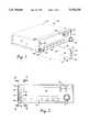
- FIG. 1is a perspective view of a storage device and receptacle according to the present invention, prior to insertion of the storage device;
- FIG. 2is a front view of the storage device and receptacle, with a power switch in an off position;
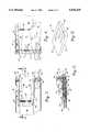
- FIG. 3is a cross-sectional left side view along line 3--3 of FIG. 2;
- FIG. 4is a cross-sectional right side view along line 4--4 of FIG. 2;
- FIG. 5is a cross-sectional plan view along line 5--5 of FIG. 3;
- FIG. 6is a perspective view showing a second embodiment of the invention.
- Storage device 10takes the general form of a card or cartridge, typically having a generally rectangular configuration.
- the storage device 10has an exterior housing 12. In the rectangular configuration shown, this will result in the device 10 having first and second major side faces 14 and 16 (16 being shown in FIG. 5) in spaced parallel relationship. Extending between these major faces are minor side faces 18, inner face 20 and outer face 22.
- these facesdefine an interior cavity 24 which houses the electronic components comprising the operative elements of the device 10.
- These componentsmay take many forms, depending upon the desired function supplied by the device 10. Typically, these components will take the form of microprocessor and/or memory elements in the form of IC chips 26. If the components 26 take the form of memory, they may be any common type, such as RAM, ROM, EPROM, etc.
- the components 26could be mounted to the interior of the cavity 24 directly, it is preferred that the components be mounted upon a printed circuit board 28, also located within the cavity.
- the board 28will typically be located in a plane parallel to the major faces 14 and 16.
- the componentswill be electrically connected to appropriate circuitry on the board, which leads to an external contact area 30 for the device. While this contact area may be located on any of the faces of the housing, it is preferred that it take the form of a standard connector operatively connected to the edge of the board closest to the inner face 20 of the housing. While the connector comprising the contact area 30 may simply be accessible through the inner face 20, in the preferred embodiment shown in FIG. 5, the connector actually serves as the inner face of the housing, thus reducing the amount of material need to form the housing. To prevent against pin bending and static electric damage, it is of course preferred that the connector be a female receptacle. Other contact arrangements, such as surface pads, may alternatively be employed.
- the housing 12will be substantially rigid, and the majority of the housing will be formed of a dielectric material, such as a non-conductive plastic.
- a conductive grounding area on the housing 12which is in electrical contact with the board 28 to permit grounding to eliminate static electric potential.
- the grounding areamay be located upon, or comprise, any of the faces 14-22.
- the grounding areaconveniently comprises the second major face 16.
- the face 16is formed of a separate sheet of material, with this material being electrically conductive and in grounding contact with the board and/or components.
- This separate sheet of materialwill typically be a metal.
- assembly of this grounding area to the remainder of the housingmay, at the same time, provide the electrical path between the grounding area and the board.
- the interior of the first major face 14may be provided with one or more mounting posts 32.
- the mounting posts 32will extend into the cavity 24 and have free ends adapted to abut against one face of the board 28.
- both the board 28 and the grounding area/major face 16will include through-holes.
- Mounting studs 34may then pass through the holes in the face 16 and board 28 and be secured to the mounting posts 32.
- This connectionmay be a threaded connection, adhesive, thermal bond, etc. This will secure the face 16 to the remainder of the housing.
- the posts 32may be formed as stepped posts, with a reduced diameter free end passing through the face 16 and board 28, and thereafter being deformed, as by thermal or ultrasonic methods, to secure these elements together.
- the electrical connection between the grounding area/face 16may be effected in various ways.
- the mounting studscould be formed of a conductive material and the through holes in the board 28 may be plated and connected to the grounding circuitry.
- the mounting holes in the face 16may be recessed to an extent such that the interior surface of the face 16 at the mounting holes contacts the surface of the board 28 at locations corresponding to grounding circuitry. This provides the added benefits that the heads of the studs 34 are recessed, and that the recesses will serve to space the board from the remainder of the face 16.
- the face 16is recessed slightly (sufficient to recess the heads of the studs 34), and one or more conductive spacers 36 (which may conveniently be standard washers) surround the studs 34 intermediate the interior surface of the face 16 and the board 28.
- the recesses and the spacerstogether serve to provide the desired spacing of the remainder of the face from the board, and also provide electrical grounding communication.
- the spacerswill contact the surface of the board 28. In some applications this will be sufficient grounding for avoiding static potential problems, without the need for connection to an actual grounding circuit.
- the spacersmay contact a grounding circuit on the board. This circuit could provide the entire ground for the components 26. Alternatively, this circuit could also be connected to a grounding pin on the pin connector forming the contacts.
- a receptacleis operatively connected to a receptacle during use.
- a receptaclemay be a dedicated, stand-alone unit used solely for reading and/or writing to the device, and which is in turn connected to other electronic equipment.
- the receptaclemay itself be the electronic equipment.
- the term "receptacle"encompasses at least these arrangements.
- reference numeral 40generally designates a receptacle 40 for use with the device 10.
- the receptacle 40is a piece of electronic equipment which reads from and/or writes to the device 10 in the performance of other functions.
- the receptacle 40may be a navigational aid for use in aircraft or watercraft which determines distances, headings, courses, etc., based upon data stored in the device 10.
- the receptacle 40may have a housing 42 which includes a front panel 44.
- the front panelmay include various buttons and or knobs 46 used to access or initiate various specialized functions.
- the receptacle 40will also include a main power switch 50 for turning the receptacle on and off.
- the receptacle 40will also include a bay 52 which receives the device 10.
- the bay 52will include an opening 54 in the housing 42 of the receptacle. In the embodiment shown in FIGS. 1-5, this opening is in the front panel 44. Additionally, in the embodiment shown, the bay is oriented vertically. This orientation permits the output display 48 to have a larger vertical extent than typical horizontal bay arrangements.
- the opening 54will have a shape which closely receives the device 10. As such, the opening will have a shape corresponding to the cross-section of the device 10 in a plane parallel to the inner face 20.
- the device 10is inserted in the proper orientation. This could be accomplished by providing the device 10 with a cross-sectional shape which is not symmetric, and the opening with a mating shape. However, this increases the complexity of the mold needed to form the housing 12. To still provide this function with reduced complexity, the device 10 is therefore provided with an alignment tail 56., best shown in FIG. 1.
- the tail 56is a cantilevered protrusion or extension of the outer face 22, extending normal to the minor faces 18. In the embodiment shown, the tail 56 is not symmetric in the cross-sectional plane. This is effected by removing a semi-circular portion from the free end of the tail adjacent the second major face 16 to define an alignment cutout 58.
- the bay 52is designed to receive a sufficient portion of the device 10 such that the tail 56 abuts against a recess in the face 44.
- the face 44is therefore provided with a recess 60 which receives the tail 56 when the device is mounted in the bay.
- the recess 60is provided with a mating configuration to the tail 56. In this manner the device 10 may only be fully received within the bay when the tail is received within the recess, which is only possible when/if the device 10 is properly oriented.
- This arrangementtherefore ensures proper orientation of the device in the receptacle.
- the production of the housing with such a tailis more complex than a housing having no tail, but is less complex than that required for many non-symmetric housing configurations.
- the race 62has a first planar side wall having a generally U-shaped configuration, with a cross bar portion 64 and first and second legs 66 and 68.
- This sidewallis arranged with the free ends of the legs adjacent the opening 54, and offset from the opening such that the sidewall will support the second major face 16 of the device.
- the racecould be provided with a second sidewall similar to the first, to thus support the first major face 14.
- the devicewould thus be received within a cavity defined by the race when in the operative position.
- the bay 52is closely adjacent to the housing 42 of the receptacle, and in particular a wall 74. As such, the free ends of the flanges 72 and 74 abut against this wall, and the wall 74 is employed to support the first major face 14.
- the race 62must of course be secured within the housing 42 of the receptacle 40.
- the free ends of the legs 66 and 68 (or the ends of the flanges 70 and 72) adjacent the opening to the bayare provided with projections 76 which are received within mating holes in the housing 42, and in particular the face 44. This secures the race adjacent the opening.
- the raceis provided with appropriate lugs 78 which are secured (possibly via other components) to the housing 42.
- the lugs 78extend across the bay at the interior end and abut against interior surface of the wall 74. Appropriate screws may secure the lugs to the wall.
- the race 62support a mating connector 80.
- the mating connectortakes the form of a male pin connector held in position by a close fit between the cross bar portion 64 of the race and the wall 74.
- the mating contactsare of course positioned such that the tail 56 of the device will be received within the recess 60 (if such are used) when the contacts 30 and 80 are in communication.
- the pin connectoris electrically connected to the electronic circuitry of the receptacle 40, in this case via a printed circuit board 82.
- the bayincludes a wiper arm 84 (FIGS. 4 and 5) extending into the bay, and in particular between the legs 66 and 68.
- the wiper armis oriented and positioned such that it will contact the grounding area of the device 10 prior to the device 10 being operatively inserted within the bay. In the embodiment shown, the wiper arm therefore contacts the second major face 16.
- the wiper arm 84is mounted to either the housing 42 (such as the face 44) or race 62, and extends toward the face 16.
- the wiper armis formed of a resilient electrically conductive material, such that it will press against the face 16 and make electrical contact.
- the wiper armis also electrically connected to a ground of the receptacle 40, typically the housing 42. As such, the face 16, and thus the board and/or components in the device 10 will be grounded prior to engagement between the contacts 30 and 80. This will ensure that any static electric potential between the device and receptacle are dissipated.
- the receptacle 10In addition to the problem of static potential, with certain types of components, it is necessary for the receptacle to be in a power off condition during insertion of the device 10. Once full insertion has been achieved, the receptacle 10 may thereafter be placed in a power-on state. Additionally or alternatively, there are applications were it is detrimental to remove the device 10 from the receptacle while the receptacle is in a power-on state. Where this is the case, the preferred embodiment provides for this.
- the power switch control 50may be placed in a position to interfere with access to the bay 52.
- the power switch controltakes the form of a rotary knob having a flange 86.
- the rotational axis of the knobis positioned relative to the opening to the bay such that the flange may extend across the opening.
- the flange 86has a portion removed to define a cut out section 88. This cut out section is angularly located such that it is over the opening when knob 50 is positioned for the power-off state, but is not over the opening when the knob is positioned for the power-on state.
- the device 10is blocked from entering or leaving the bay when the knob 50 is in the power-on position. This eliminates the possibility of inadvertent insertion or removal of the device at a time which prevents operation or might cause damage.
- a similar arrangementmay be achieved with power switches of other types.
- a sliding switchcould allow access during power-off, but block the opening during power-on.
- the circular periphery of the knob 50 at the cut out 88may correspond to the cut out 58 in the tail 56 of the device 10, thus combining the orientation/polarization assurance with the insertion/removal assurance.
- the outer face 22may be substantially flush with the panel 44 of the receptacle. Where this is the case, it is preferred to provide the device 10 with a handle 90 on its outer face. This will clearly facilitate manual grasping of the device for removal from the bay. By permitting this manual removal, there is no need for a costly ejector mechanism.
- FIG. 6a second embodiment of a device 10 is shown.
- the majority of componentsare identical to the first, with the exception of the arrangement for assuring proper orientation.
- the tailhas been removed, and the first major face 14' is provided with a plurality of ribs 92 extending in a direction parallel to the insertion and removal direction.
- the opening of the bay(not shown) may then have appropriate mating recesses, assuring proper orientation.
- a second differenceis the handle 90', which in this embodiment extends the full length of the outer face 22'.
- the opening to the baymay be located on a bottom face of the housing to reduce the possibility of water ingress.
Landscapes
- Engineering & Computer Science (AREA)
- Microelectronics & Electronic Packaging (AREA)
- Physics & Mathematics (AREA)
- General Physics & Mathematics (AREA)
- Theoretical Computer Science (AREA)
- Computer Networks & Wireless Communication (AREA)
- Signal Processing (AREA)
- Details Of Connecting Devices For Male And Female Coupling (AREA)
Abstract
Description
Claims (21)
Priority Applications (1)
| Application Number | Priority Date | Filing Date | Title |
|---|---|---|---|
| US08/265,006US5526235A (en) | 1994-06-23 | 1994-06-23 | Electronic storage device and receptacle |
Applications Claiming Priority (1)
| Application Number | Priority Date | Filing Date | Title |
|---|---|---|---|
| US08/265,006US5526235A (en) | 1994-06-23 | 1994-06-23 | Electronic storage device and receptacle |
Publications (1)
| Publication Number | Publication Date |
|---|---|
| US5526235Atrue US5526235A (en) | 1996-06-11 |
Family
ID=23008561
Family Applications (1)
| Application Number | Title | Priority Date | Filing Date |
|---|---|---|---|
| US08/265,006Expired - LifetimeUS5526235A (en) | 1994-06-23 | 1994-06-23 | Electronic storage device and receptacle |
Country Status (1)
| Country | Link |
|---|---|
| US (1) | US5526235A (en) |
Cited By (15)
| Publication number | Priority date | Publication date | Assignee | Title |
|---|---|---|---|---|
| US5719753A (en)* | 1995-02-03 | 1998-02-17 | Cliff Electronic Components Limited | Circuit board assembly |
| US6215671B1 (en) | 1998-12-10 | 2001-04-10 | Garmin Corporation | Method and apparatus for connecting circuit boards |
| US6250553B1 (en) | 1998-12-30 | 2001-06-26 | Garmin Corporation | Data card having a retractable handle |
| US6282097B1 (en) | 1998-10-28 | 2001-08-28 | Garmin Corporation | Data card having a retractable handle |
| US6527227B1 (en) | 2001-08-16 | 2003-03-04 | The Boeing Company | Storage compartment with universal mounting capability |
| US6644550B1 (en)* | 2002-07-03 | 2003-11-11 | Hon Hai Precision Ind. Co., Ltd. | Electrical card connector having blocking means |
| US20040212959A1 (en)* | 2003-04-25 | 2004-10-28 | Rotta Phillip R. | Fixture and method for quick installation and removal of mobile platform electronic modules |
| US20050088832A1 (en)* | 2003-10-24 | 2005-04-28 | Po-Chang Su | ESD protection structure and device utilizing the same |
| US20060010000A1 (en)* | 2004-07-06 | 2006-01-12 | Joachim Jauert | Arrangement for installing a communication unit in an apparatus |
| USRE40150E1 (en) | 1994-04-25 | 2008-03-11 | Matsushita Electric Industrial Co., Ltd. | Fiber optic module |
| US20080165508A1 (en)* | 2007-01-05 | 2008-07-10 | Apple Inc. | Ejectable component assemblies in electronic devices |
| US20090200381A1 (en)* | 2004-06-30 | 2009-08-13 | Koninklijke Philips Electronics N.V. | Chip card for insertion into a holder |
| US7616977B1 (en)* | 2005-01-28 | 2009-11-10 | Scott David Nortman | Method and apparatus for motorized control of an automobile radio cover |
| US7908080B2 (en) | 2004-12-31 | 2011-03-15 | Google Inc. | Transportation routing |
| US20110111803A1 (en)* | 2008-11-27 | 2011-05-12 | Mitsubishi Electric Corporation | Radio base station device |
Citations (34)
| Publication number | Priority date | Publication date | Assignee | Title |
|---|---|---|---|---|
| US4138711A (en)* | 1977-09-29 | 1979-02-06 | Allen-Bradley Company | Static control device for printed circuit package |
| US4531176A (en)* | 1983-06-27 | 1985-07-23 | At&T Bell Laboratories | Cartridge having improved electrostatic discharge protection |
| US4780604A (en)* | 1986-02-21 | 1988-10-25 | Kabushiki Kaisha Toshiba | IC-incorporated memory card |
| US4780791A (en)* | 1986-04-08 | 1988-10-25 | Fujisoku Electric Co., Ltd. | Card-shaped memory having an IC module |
| US4780793A (en)* | 1986-06-03 | 1988-10-25 | Daiichi Denshi Kogyo Kabushiki Kaisha | IC card and connector therefor |
| US4868715A (en)* | 1988-05-31 | 1989-09-19 | Scosche Industries, Inc. | Break-away panel structure for radio in-dash installation kit |
| US4872091A (en)* | 1986-07-21 | 1989-10-03 | Ricoh Company, Ltd. | Memory cartridge |
| US4905124A (en)* | 1987-03-31 | 1990-02-27 | Mitsubishi Denki Kabushiki Kaisha | IC card |
| US4956756A (en)* | 1989-02-10 | 1990-09-11 | Hsiao Wen J | Table lamp adapter system |
| US4955817A (en)* | 1988-02-12 | 1990-09-11 | Seiko Epson Corporation | Construction for removing electronic charges in connectors |
| US4974120A (en)* | 1989-01-12 | 1990-11-27 | Mitsubishi Denki Kabushiki Kaisha | IC card |
| US5017767A (en)* | 1987-08-31 | 1991-05-21 | Fanuc Ltd. | IC card with metal reinforcing plates and grounding lead wire |
| US5031076A (en)* | 1988-12-06 | 1991-07-09 | E. I. Du Pont De Nemours And Company | Multifunctional card having a static protection |
| US5053613A (en)* | 1990-05-29 | 1991-10-01 | Mitsubishi Denki Kabushiki Kaisha | IC card |
| US5068765A (en)* | 1990-02-06 | 1991-11-26 | Scosche Industries, Inc. | Marine stereo cover with detenting hinge |
| US5151774A (en)* | 1990-10-31 | 1992-09-29 | Mitsubishi Denki Kabushiki Kaisha | Portable semiconductor data storage device with disconnectable ground connection |
| US5153818A (en)* | 1990-04-20 | 1992-10-06 | Rohm Co., Ltd. | Ic memory card with an anisotropic conductive rubber interconnector |
| US5161169A (en)* | 1990-05-15 | 1992-11-03 | Codex Corporation | Dcd with reprogramming instructions contained in removable cartridge |
| US5173840A (en)* | 1990-05-07 | 1992-12-22 | Mitsubishi Denki Kabushiki Kaisha | Molded ic card |
| US5229925A (en)* | 1991-07-19 | 1993-07-20 | Valcom, Inc. | Modular front panel and enclosure for electronic apparatus |
| US5288237A (en)* | 1992-01-08 | 1994-02-22 | Mitsubishi Denki Kabushiki Kaisha | IC card connector supporting/fixing mechanism |
| US5319516A (en)* | 1991-09-09 | 1994-06-07 | Itt Corporation | Electrostatically protected IC card |
| US5330360A (en)* | 1992-08-21 | 1994-07-19 | The Whitaker Corporation | Memory card and connector therefor |
| US5335145A (en)* | 1992-06-16 | 1994-08-02 | Mitsubishi Denki Kabushiki Kaisha | IC card and method of manufacturing the same |
| US5339222A (en)* | 1993-04-06 | 1994-08-16 | The Whitaker Corporation | Shielded printed circuit card holder |
| US5357402A (en)* | 1992-02-24 | 1994-10-18 | Itt Corporation | Card-receiving electronic device having grounding spring |
| US5375037A (en)* | 1992-01-14 | 1994-12-20 | Gemplus Card International | Memory card having a recessed portion with contacts connected to an access card |
| US5386340A (en)* | 1993-08-13 | 1995-01-31 | Kurz; Arthur A. | Enclosure for personal computer card GPT |
| US5397857A (en)* | 1993-07-15 | 1995-03-14 | Dual Systems | PCMCIA standard memory card frame |
| US5408385A (en)* | 1993-04-30 | 1995-04-18 | Robertshaw Controls Company | Control device and method of making the same |
| US5414253A (en)* | 1991-12-03 | 1995-05-09 | Texas Instruments Incorporated | Integrated circuit card |
| US5440448A (en)* | 1992-06-22 | 1995-08-08 | Dell Usa, L.P. | Electronic system with compact card ejector |
| US5440451A (en)* | 1992-12-29 | 1995-08-08 | Casio Computer Co., Ltd. | Memory Assembly |
| US5446622A (en)* | 1993-08-06 | 1995-08-29 | Digital Equipment Corporation | PC board cartridge for a computer terminal |
- 1994
- 1994-06-23USUS08/265,006patent/US5526235A/ennot_activeExpired - Lifetime
Patent Citations (34)
| Publication number | Priority date | Publication date | Assignee | Title |
|---|---|---|---|---|
| US4138711A (en)* | 1977-09-29 | 1979-02-06 | Allen-Bradley Company | Static control device for printed circuit package |
| US4531176A (en)* | 1983-06-27 | 1985-07-23 | At&T Bell Laboratories | Cartridge having improved electrostatic discharge protection |
| US4780604A (en)* | 1986-02-21 | 1988-10-25 | Kabushiki Kaisha Toshiba | IC-incorporated memory card |
| US4780791A (en)* | 1986-04-08 | 1988-10-25 | Fujisoku Electric Co., Ltd. | Card-shaped memory having an IC module |
| US4780793A (en)* | 1986-06-03 | 1988-10-25 | Daiichi Denshi Kogyo Kabushiki Kaisha | IC card and connector therefor |
| US4872091A (en)* | 1986-07-21 | 1989-10-03 | Ricoh Company, Ltd. | Memory cartridge |
| US4905124A (en)* | 1987-03-31 | 1990-02-27 | Mitsubishi Denki Kabushiki Kaisha | IC card |
| US5017767A (en)* | 1987-08-31 | 1991-05-21 | Fanuc Ltd. | IC card with metal reinforcing plates and grounding lead wire |
| US4955817A (en)* | 1988-02-12 | 1990-09-11 | Seiko Epson Corporation | Construction for removing electronic charges in connectors |
| US4868715A (en)* | 1988-05-31 | 1989-09-19 | Scosche Industries, Inc. | Break-away panel structure for radio in-dash installation kit |
| US5031076A (en)* | 1988-12-06 | 1991-07-09 | E. I. Du Pont De Nemours And Company | Multifunctional card having a static protection |
| US4974120A (en)* | 1989-01-12 | 1990-11-27 | Mitsubishi Denki Kabushiki Kaisha | IC card |
| US4956756A (en)* | 1989-02-10 | 1990-09-11 | Hsiao Wen J | Table lamp adapter system |
| US5068765A (en)* | 1990-02-06 | 1991-11-26 | Scosche Industries, Inc. | Marine stereo cover with detenting hinge |
| US5153818A (en)* | 1990-04-20 | 1992-10-06 | Rohm Co., Ltd. | Ic memory card with an anisotropic conductive rubber interconnector |
| US5173840A (en)* | 1990-05-07 | 1992-12-22 | Mitsubishi Denki Kabushiki Kaisha | Molded ic card |
| US5161169A (en)* | 1990-05-15 | 1992-11-03 | Codex Corporation | Dcd with reprogramming instructions contained in removable cartridge |
| US5053613A (en)* | 1990-05-29 | 1991-10-01 | Mitsubishi Denki Kabushiki Kaisha | IC card |
| US5151774A (en)* | 1990-10-31 | 1992-09-29 | Mitsubishi Denki Kabushiki Kaisha | Portable semiconductor data storage device with disconnectable ground connection |
| US5229925A (en)* | 1991-07-19 | 1993-07-20 | Valcom, Inc. | Modular front panel and enclosure for electronic apparatus |
| US5319516A (en)* | 1991-09-09 | 1994-06-07 | Itt Corporation | Electrostatically protected IC card |
| US5414253A (en)* | 1991-12-03 | 1995-05-09 | Texas Instruments Incorporated | Integrated circuit card |
| US5288237A (en)* | 1992-01-08 | 1994-02-22 | Mitsubishi Denki Kabushiki Kaisha | IC card connector supporting/fixing mechanism |
| US5375037A (en)* | 1992-01-14 | 1994-12-20 | Gemplus Card International | Memory card having a recessed portion with contacts connected to an access card |
| US5357402A (en)* | 1992-02-24 | 1994-10-18 | Itt Corporation | Card-receiving electronic device having grounding spring |
| US5335145A (en)* | 1992-06-16 | 1994-08-02 | Mitsubishi Denki Kabushiki Kaisha | IC card and method of manufacturing the same |
| US5440448A (en)* | 1992-06-22 | 1995-08-08 | Dell Usa, L.P. | Electronic system with compact card ejector |
| US5330360A (en)* | 1992-08-21 | 1994-07-19 | The Whitaker Corporation | Memory card and connector therefor |
| US5440451A (en)* | 1992-12-29 | 1995-08-08 | Casio Computer Co., Ltd. | Memory Assembly |
| US5339222A (en)* | 1993-04-06 | 1994-08-16 | The Whitaker Corporation | Shielded printed circuit card holder |
| US5408385A (en)* | 1993-04-30 | 1995-04-18 | Robertshaw Controls Company | Control device and method of making the same |
| US5397857A (en)* | 1993-07-15 | 1995-03-14 | Dual Systems | PCMCIA standard memory card frame |
| US5446622A (en)* | 1993-08-06 | 1995-08-29 | Digital Equipment Corporation | PC board cartridge for a computer terminal |
| US5386340A (en)* | 1993-08-13 | 1995-01-31 | Kurz; Arthur A. | Enclosure for personal computer card GPT |
Cited By (37)
| Publication number | Priority date | Publication date | Assignee | Title |
|---|---|---|---|---|
| USRE40150E1 (en) | 1994-04-25 | 2008-03-11 | Matsushita Electric Industrial Co., Ltd. | Fiber optic module |
| USRE40154E1 (en) | 1994-04-25 | 2008-03-18 | Matsushita Electric Industrial Co., Ltd. | Fiber optic module |
| US5719753A (en)* | 1995-02-03 | 1998-02-17 | Cliff Electronic Components Limited | Circuit board assembly |
| US6282097B1 (en) | 1998-10-28 | 2001-08-28 | Garmin Corporation | Data card having a retractable handle |
| US6368115B2 (en) | 1998-12-10 | 2002-04-09 | Garmin Corporation | Method and apparatus for connecting circuit boards |
| US6215671B1 (en) | 1998-12-10 | 2001-04-10 | Garmin Corporation | Method and apparatus for connecting circuit boards |
| US6250553B1 (en) | 1998-12-30 | 2001-06-26 | Garmin Corporation | Data card having a retractable handle |
| US6527227B1 (en) | 2001-08-16 | 2003-03-04 | The Boeing Company | Storage compartment with universal mounting capability |
| US6644550B1 (en)* | 2002-07-03 | 2003-11-11 | Hon Hai Precision Ind. Co., Ltd. | Electrical card connector having blocking means |
| US20040212959A1 (en)* | 2003-04-25 | 2004-10-28 | Rotta Phillip R. | Fixture and method for quick installation and removal of mobile platform electronic modules |
| US6914781B2 (en) | 2003-04-25 | 2005-07-05 | The Boeing Company | Fixture and method for quick installation and removal of mobile platform electronic modules |
| US20050088832A1 (en)* | 2003-10-24 | 2005-04-28 | Po-Chang Su | ESD protection structure and device utilizing the same |
| US7088592B2 (en)* | 2003-10-24 | 2006-08-08 | Asustek Computer Inc. | ESD protection structure and device utilizing the same |
| US20090200381A1 (en)* | 2004-06-30 | 2009-08-13 | Koninklijke Philips Electronics N.V. | Chip card for insertion into a holder |
| US8695881B2 (en)* | 2004-06-30 | 2014-04-15 | Nxp B.V. | Chip card for insertion into a holder |
| US20060010000A1 (en)* | 2004-07-06 | 2006-01-12 | Joachim Jauert | Arrangement for installing a communication unit in an apparatus |
| US8004858B2 (en)* | 2004-07-06 | 2011-08-23 | Francotyp-Postalia Gmbh | Arrangement for installing a communication unit in an apparatus |
| US9945686B2 (en) | 2004-12-31 | 2018-04-17 | Google Llc | Transportation routing |
| US8606514B2 (en) | 2004-12-31 | 2013-12-10 | Google Inc. | Transportation routing |
| US7908080B2 (en) | 2004-12-31 | 2011-03-15 | Google Inc. | Transportation routing |
| US9778055B2 (en) | 2004-12-31 | 2017-10-03 | Google Inc. | Transportation routing |
| US9709415B2 (en) | 2004-12-31 | 2017-07-18 | Google Inc. | Transportation routing |
| US8798917B2 (en) | 2004-12-31 | 2014-08-05 | Google Inc. | Transportation routing |
| US11092455B2 (en) | 2004-12-31 | 2021-08-17 | Google Llc | Transportation routing |
| US7616977B1 (en)* | 2005-01-28 | 2009-11-10 | Scott David Nortman | Method and apparatus for motorized control of an automobile radio cover |
| US7865210B2 (en) | 2007-01-05 | 2011-01-04 | Apple Inc. | Ejectable component assemblies in electronic devices |
| US8725198B2 (en) | 2007-01-05 | 2014-05-13 | Apple Inc. | Ejectable component assemblies in electronic devices |
| US8145261B2 (en) | 2007-01-05 | 2012-03-27 | Apple Inc. | Ejectable component assemblies in electronic devices |
| US9504179B2 (en) | 2007-01-05 | 2016-11-22 | Apple Inc. | Ejectable component assemblies in electronic devices |
| US20110080699A1 (en)* | 2007-01-05 | 2011-04-07 | Apple Inc. | Ejectable component assemblies in electronic devices |
| WO2008085930A3 (en)* | 2007-01-05 | 2009-06-11 | Apple Inc | Ejectable component assemblies in electronic devices |
| US10277722B2 (en) | 2007-01-05 | 2019-04-30 | Apple Inc. | Ejectable component assemblies in electronic devices |
| US11050865B2 (en) | 2007-01-05 | 2021-06-29 | Apple Inc. | Ejectable component assemblies in electronic devices |
| US20080165508A1 (en)* | 2007-01-05 | 2008-07-10 | Apple Inc. | Ejectable component assemblies in electronic devices |
| US8244302B2 (en)* | 2008-11-27 | 2012-08-14 | Mitsubishi Electric Corporation | Radio base station device |
| CN102090136B (en)* | 2008-11-27 | 2016-08-17 | 三菱电机株式会社 | Radio base station apparatus |
| US20110111803A1 (en)* | 2008-11-27 | 2011-05-12 | Mitsubishi Electric Corporation | Radio base station device |
Similar Documents
| Publication | Publication Date | Title |
|---|---|---|
| US5526235A (en) | Electronic storage device and receptacle | |
| US5216582A (en) | Shock mounted disk drive module having snap-lock cover | |
| EP0532166B1 (en) | Memory card grounding apparatus | |
| US6761572B1 (en) | Mini memory card connector | |
| US5583745A (en) | Data recording and reproducing device comprising a memory unit used for a memory card | |
| EP0738102B1 (en) | Reduced static raid enclosure | |
| KR200356231Y1 (en) | Multi-in-one connector structure | |
| US4216522A (en) | Interchangeable module for integrated circuits | |
| US20100317205A1 (en) | Electronic card with protecting mechanism for protecting contacts thereof | |
| EP0281277B1 (en) | Improved receptacle device | |
| JPH07270457A (en) | Digital Multimeters | |
| US4595804A (en) | Auxiliary keyboard | |
| US4919624A (en) | Connection terminal structure of electronic equipment | |
| US20040105230A1 (en) | Case for portable storage peripheral equipment having cable assembly with strain relief | |
| JP2013093233A (en) | Card connector | |
| EP1133221B1 (en) | Electronic device and case | |
| US4905173A (en) | Hardened shop-floor data terminal | |
| JPH10255910A (en) | Ic card connector | |
| US20010021606A1 (en) | IC card connector having a shutter mechanism | |
| US6717818B1 (en) | Case for portable storage peripheral equipment having improved shielding effect | |
| JP3584021B2 (en) | External storage unit and information processing apparatus having the same | |
| US7080995B2 (en) | Electrical card connector having dustproof device | |
| JP3426545B2 (en) | IC card connector | |
| US6437992B1 (en) | Hot pluggable printed circuit board insulating system and method | |
| KR20030017326A (en) | Cartridge for game machine |
Legal Events
| Date | Code | Title | Description |
|---|---|---|---|
| AS | Assignment | Owner name:GARMIN COMMUNICATION AND NAVIGATION, KANSAS Free format text:ASSIGNMENT OF ASSIGNORS INTEREST;ASSIGNORS:BEASON, LAWRENCE W.;WHEATON, SHELDON T.;HANSHEW, CHRISTOPHER J.;REEL/FRAME:007051/0232 Effective date:19940621 | |
| STCF | Information on status: patent grant | Free format text:PATENTED CASE | |
| FEPP | Fee payment procedure | Free format text:PAYOR NUMBER ASSIGNED (ORIGINAL EVENT CODE: ASPN); ENTITY STATUS OF PATENT OWNER: LARGE ENTITY Free format text:PAT HLDR NO LONGER CLAIMS SMALL ENT STAT AS INDIV INVENTOR (ORIGINAL EVENT CODE: LSM1); ENTITY STATUS OF PATENT OWNER: LARGE ENTITY | |
| AS | Assignment | Owner name:GARMIN CORPORATION, TAIWAN Free format text:ASSIGNMENT OF ASSIGNORS INTEREST;ASSIGNORS:BEASON, LAWRENCE W.;WHEATON, SHELTON T.;HANSHWE, CHRISTOPHER J.;REEL/FRAME:010052/0352 Effective date:19990617 | |
| FPAY | Fee payment | Year of fee payment:4 | |
| FEPP | Fee payment procedure | Free format text:PAYOR NUMBER ASSIGNED (ORIGINAL EVENT CODE: ASPN); ENTITY STATUS OF PATENT OWNER: LARGE ENTITY Free format text:PAYER NUMBER DE-ASSIGNED (ORIGINAL EVENT CODE: RMPN); ENTITY STATUS OF PATENT OWNER: LARGE ENTITY | |
| FPAY | Fee payment | Year of fee payment:8 | |
| FPAY | Fee payment | Year of fee payment:12 |