US5524339A - Method for protecting gallium arsenide mmic air bridge structures - Google Patents
Method for protecting gallium arsenide mmic air bridge structuresDownload PDFInfo
- Publication number
- US5524339A US5524339AUS08/308,886US30888694AUS5524339AUS 5524339 AUS5524339 AUS 5524339AUS 30888694 AUS30888694 AUS 30888694AUS 5524339 AUS5524339 AUS 5524339A
- Authority
- US
- United States
- Prior art keywords
- sensitive structure
- layer
- protective layer
- making
- high density
- Prior art date
- Legal status (The legal status is an assumption and is not a legal conclusion. Google has not performed a legal analysis and makes no representation as to the accuracy of the status listed.)
- Expired - Lifetime
Links
- 238000000034methodMethods0.000titleclaimsabstractdescription41
- JBRZTFJDHDCESZ-UHFFFAOYSA-NAsGaChemical compound[As]#[Ga]JBRZTFJDHDCESZ-UHFFFAOYSA-N0.000titledescription6
- 229910001218Gallium arsenideInorganic materials0.000titledescription5
- 239000011241protective layerSubstances0.000claimsabstractdescription24
- 238000011109contaminationMethods0.000claimsabstract3
- 239000010410layerSubstances0.000claimsdescription79
- 239000000758substrateSubstances0.000claimsdescription31
- 239000004020conductorSubstances0.000claimsdescription11
- 229930195733hydrocarbonNatural products0.000claimsdescription9
- 150000002430hydrocarbonsChemical class0.000claimsdescription9
- 239000004215Carbon black (E152)Substances0.000claimsdescription8
- 238000012545processingMethods0.000claimsdescription8
- ZWEHNKRNPOVVGH-UHFFFAOYSA-N2-ButanoneChemical compoundCCC(C)=OZWEHNKRNPOVVGH-UHFFFAOYSA-N0.000claimsdescription6
- 229910052581Si3N4Inorganic materials0.000claimsdescription3
- 150000001721carbonChemical class0.000claimsdescription3
- HQVNEWCFYHHQES-UHFFFAOYSA-Nsilicon nitrideChemical groupN12[Si]34N5[Si]62N3[Si]51N64HQVNEWCFYHHQES-UHFFFAOYSA-N0.000claimsdescription3
- 238000002679ablationMethods0.000claimsdescription2
- 238000009835boilingMethods0.000claimsdescription2
- 230000001681protective effectEffects0.000abstractdescription13
- 238000001465metallisationMethods0.000description25
- 239000000853adhesiveSubstances0.000description23
- 230000001070adhesive effectEffects0.000description23
- 239000000463materialSubstances0.000description20
- 230000008569processEffects0.000description15
- 238000003475laminationMethods0.000description10
- 238000004519manufacturing processMethods0.000description9
- 229920001169thermoplasticPolymers0.000description8
- 239000004416thermosoftening plasticSubstances0.000description8
- 229910003481amorphous carbonInorganic materials0.000description7
- 230000008901benefitEffects0.000description7
- 229920003223poly(pyromellitimide-1,4-diphenyl ether)Polymers0.000description7
- 239000011347resinSubstances0.000description7
- 229920005989resinPolymers0.000description7
- 239000004065semiconductorSubstances0.000description7
- OKTJSMMVPCPJKN-UHFFFAOYSA-NCarbonChemical compound[C]OKTJSMMVPCPJKN-UHFFFAOYSA-N0.000description5
- 239000004697PolyetherimideSubstances0.000description5
- 239000004642PolyimideSubstances0.000description5
- 229920004738ULTEM®Polymers0.000description5
- 238000000151depositionMethods0.000description5
- 239000000203mixtureSubstances0.000description5
- 229920001601polyetherimidePolymers0.000description5
- 229920001721polyimidePolymers0.000description5
- 125000006850spacer groupChemical group0.000description5
- 229920001187thermosetting polymerPolymers0.000description5
- 229910052799carbonInorganic materials0.000description4
- 239000010949copperSubstances0.000description4
- 230000008021depositionEffects0.000description4
- 239000003989dielectric materialSubstances0.000description4
- 238000000608laser ablationMethods0.000description4
- 238000004806packaging method and processMethods0.000description4
- 238000001020plasma etchingMethods0.000description4
- 239000010936titaniumSubstances0.000description4
- RYGMFSIKBFXOCR-UHFFFAOYSA-NCopperChemical compound[Cu]RYGMFSIKBFXOCR-UHFFFAOYSA-N0.000description3
- YMWUJEATGCHHMB-UHFFFAOYSA-NDichloromethaneChemical compoundClCClYMWUJEATGCHHMB-UHFFFAOYSA-N0.000description3
- 239000004593EpoxySubstances0.000description3
- 239000002318adhesion promoterSubstances0.000description3
- 229910052802copperInorganic materials0.000description3
- 238000013461designMethods0.000description3
- 238000005553drillingMethods0.000description3
- 230000000694effectsEffects0.000description3
- 239000002904solventSubstances0.000description3
- 239000000126substanceSubstances0.000description3
- 238000012360testing methodMethods0.000description3
- CSCPPACGZOOCGX-UHFFFAOYSA-NAcetoneChemical compoundCC(C)=OCSCPPACGZOOCGX-UHFFFAOYSA-N0.000description2
- ATUOYWHBWRKTHZ-UHFFFAOYSA-NPropaneChemical compoundCCCATUOYWHBWRKTHZ-UHFFFAOYSA-N0.000description2
- RTAQQCXQSZGOHL-UHFFFAOYSA-NTitaniumChemical compound[Ti]RTAQQCXQSZGOHL-UHFFFAOYSA-N0.000description2
- QVGXLLKOCUKJST-UHFFFAOYSA-Natomic oxygenChemical compound[O]QVGXLLKOCUKJST-UHFFFAOYSA-N0.000description2
- 230000005540biological transmissionEffects0.000description2
- 239000000919ceramicSubstances0.000description2
- KPUWHANPEXNPJT-UHFFFAOYSA-NdisiloxaneChemical class[SiH3]O[SiH3]KPUWHANPEXNPJT-UHFFFAOYSA-N0.000description2
- 229910021385hard carbonInorganic materials0.000description2
- 238000010030laminatingMethods0.000description2
- 239000002184metalSubstances0.000description2
- 229910052751metalInorganic materials0.000description2
- VNWKTOKETHGBQD-UHFFFAOYSA-NmethaneChemical compoundCVNWKTOKETHGBQD-UHFFFAOYSA-N0.000description2
- 238000003801millingMethods0.000description2
- 230000004048modificationEffects0.000description2
- 238000012986modificationMethods0.000description2
- 229910052760oxygenInorganic materials0.000description2
- 239000001301oxygenSubstances0.000description2
- 229920002120photoresistant polymerPolymers0.000description2
- 230000002829reductive effectEffects0.000description2
- 229910052719titaniumInorganic materials0.000description2
- LUNMJRJMSXZSLC-UHFFFAOYSA-N2-cyclopropylethanolChemical compoundOCCC1CC1LUNMJRJMSXZSLC-UHFFFAOYSA-N0.000description1
- 229910000661Mercury cadmium tellurideInorganic materials0.000description1
- 229920004747ULTEM® 1000Polymers0.000description1
- 230000003044adaptive effectEffects0.000description1
- 239000012790adhesive layerSubstances0.000description1
- 230000002411adverseEffects0.000description1
- 150000001298alcoholsChemical class0.000description1
- 150000001299aldehydesChemical class0.000description1
- PNEYBMLMFCGWSK-UHFFFAOYSA-Naluminium oxideInorganic materials[O-2].[O-2].[O-2].[Al+3].[Al+3]PNEYBMLMFCGWSK-UHFFFAOYSA-N0.000description1
- 238000004380ashingMethods0.000description1
- 230000015572biosynthetic processEffects0.000description1
- -1butanone liquidChemical class0.000description1
- 239000006227byproductSubstances0.000description1
- 230000008859changeEffects0.000description1
- 238000004140cleaningMethods0.000description1
- 239000000356contaminantSubstances0.000description1
- 229920001577copolymerPolymers0.000description1
- 230000008878couplingEffects0.000description1
- 238000010168coupling processMethods0.000description1
- 238000005859coupling reactionMethods0.000description1
- 238000004132cross linkingMethods0.000description1
- 230000007423decreaseEffects0.000description1
- 238000005137deposition processMethods0.000description1
- 229910003460diamondInorganic materials0.000description1
- 239000010432diamondSubstances0.000description1
- 238000009713electroplatingMethods0.000description1
- 238000005538encapsulationMethods0.000description1
- 238000005530etchingMethods0.000description1
- 230000009477glass transitionEffects0.000description1
- 230000006872improvementEffects0.000description1
- WPYVAWXEWQSOGY-UHFFFAOYSA-Nindium antimonideChemical compound[Sb]#[In]WPYVAWXEWQSOGY-UHFFFAOYSA-N0.000description1
- 230000002401inhibitory effectEffects0.000description1
- 239000007788liquidSubstances0.000description1
- 238000001459lithographyMethods0.000description1
- 230000000873masking effectEffects0.000description1
- 238000005259measurementMethods0.000description1
- 238000004377microelectronicMethods0.000description1
- 231100000989no adverse effectToxicity0.000description1
- 239000000615nonconductorSubstances0.000description1
- 229920000642polymerPolymers0.000description1
- 230000000750progressive effectEffects0.000description1
- BDERNNFJNOPAEC-UHFFFAOYSA-Npropan-1-olChemical compoundCCCOBDERNNFJNOPAEC-UHFFFAOYSA-N0.000description1
- 239000001294propaneSubstances0.000description1
- 230000008439repair processEffects0.000description1
- 238000011160researchMethods0.000description1
- 238000007665saggingMethods0.000description1
- 239000000523sampleSubstances0.000description1
- 238000002791soakingMethods0.000description1
- 239000012815thermoplastic materialSubstances0.000description1
- WCLDITPGPXSPGV-UHFFFAOYSA-NtricambaChemical compoundCOC1=C(Cl)C=C(Cl)C(Cl)=C1C(O)=OWCLDITPGPXSPGV-UHFFFAOYSA-N0.000description1
- 239000011800void materialSubstances0.000description1
Images

Classifications
- H—ELECTRICITY
- H01—ELECTRIC ELEMENTS
- H01L—SEMICONDUCTOR DEVICES NOT COVERED BY CLASS H10
- H01L23/00—Details of semiconductor or other solid state devices
- H01L23/562—Protection against mechanical damage
- H—ELECTRICITY
- H01—ELECTRIC ELEMENTS
- H01L—SEMICONDUCTOR DEVICES NOT COVERED BY CLASS H10
- H01L23/00—Details of semiconductor or other solid state devices
- H01L23/28—Encapsulations, e.g. encapsulating layers, coatings, e.g. for protection
- H01L23/29—Encapsulations, e.g. encapsulating layers, coatings, e.g. for protection characterised by the material, e.g. carbon
- H—ELECTRICITY
- H01—ELECTRIC ELEMENTS
- H01L—SEMICONDUCTOR DEVICES NOT COVERED BY CLASS H10
- H01L23/00—Details of semiconductor or other solid state devices
- H01L23/28—Encapsulations, e.g. encapsulating layers, coatings, e.g. for protection
- H01L23/31—Encapsulations, e.g. encapsulating layers, coatings, e.g. for protection characterised by the arrangement or shape
- H01L23/3107—Encapsulations, e.g. encapsulating layers, coatings, e.g. for protection characterised by the arrangement or shape the device being completely enclosed
- H01L23/315—Encapsulations, e.g. encapsulating layers, coatings, e.g. for protection characterised by the arrangement or shape the device being completely enclosed the encapsulation having a cavity
- H—ELECTRICITY
- H01—ELECTRIC ELEMENTS
- H01L—SEMICONDUCTOR DEVICES NOT COVERED BY CLASS H10
- H01L23/00—Details of semiconductor or other solid state devices
- H01L23/52—Arrangements for conducting electric current within the device in operation from one component to another, i.e. interconnections, e.g. wires, lead frames
- H01L23/538—Arrangements for conducting electric current within the device in operation from one component to another, i.e. interconnections, e.g. wires, lead frames the interconnection structure between a plurality of semiconductor chips being formed on, or in, insulating substrates
- H01L23/5385—Assembly of a plurality of insulating substrates
- H—ELECTRICITY
- H01—ELECTRIC ELEMENTS
- H01L—SEMICONDUCTOR DEVICES NOT COVERED BY CLASS H10
- H01L23/00—Details of semiconductor or other solid state devices
- H01L23/52—Arrangements for conducting electric current within the device in operation from one component to another, i.e. interconnections, e.g. wires, lead frames
- H01L23/538—Arrangements for conducting electric current within the device in operation from one component to another, i.e. interconnections, e.g. wires, lead frames the interconnection structure between a plurality of semiconductor chips being formed on, or in, insulating substrates
- H01L23/5389—Arrangements for conducting electric current within the device in operation from one component to another, i.e. interconnections, e.g. wires, lead frames the interconnection structure between a plurality of semiconductor chips being formed on, or in, insulating substrates the chips being integrally enclosed by the interconnect and support structures
- H—ELECTRICITY
- H01—ELECTRIC ELEMENTS
- H01L—SEMICONDUCTOR DEVICES NOT COVERED BY CLASS H10
- H01L23/00—Details of semiconductor or other solid state devices
- H01L23/58—Structural electrical arrangements for semiconductor devices not otherwise provided for, e.g. in combination with batteries
- H01L23/64—Impedance arrangements
- H01L23/66—High-frequency adaptations
- H—ELECTRICITY
- H01—ELECTRIC ELEMENTS
- H01L—SEMICONDUCTOR DEVICES NOT COVERED BY CLASS H10
- H01L24/00—Arrangements for connecting or disconnecting semiconductor or solid-state bodies; Methods or apparatus related thereto
- H01L24/01—Means for bonding being attached to, or being formed on, the surface to be connected, e.g. chip-to-package, die-attach, "first-level" interconnects; Manufacturing methods related thereto
- H01L24/18—High density interconnect [HDI] connectors; Manufacturing methods related thereto
- H01L24/23—Structure, shape, material or disposition of the high density interconnect connectors after the connecting process
- H01L24/24—Structure, shape, material or disposition of the high density interconnect connectors after the connecting process of an individual high density interconnect connector
- H—ELECTRICITY
- H01—ELECTRIC ELEMENTS
- H01L—SEMICONDUCTOR DEVICES NOT COVERED BY CLASS H10
- H01L24/00—Arrangements for connecting or disconnecting semiconductor or solid-state bodies; Methods or apparatus related thereto
- H01L24/80—Methods for connecting semiconductor or other solid state bodies using means for bonding being attached to, or being formed on, the surface to be connected
- H01L24/82—Methods for connecting semiconductor or other solid state bodies using means for bonding being attached to, or being formed on, the surface to be connected by forming build-up interconnects at chip-level, e.g. for high density interconnects [HDI]
- H—ELECTRICITY
- H01—ELECTRIC ELEMENTS
- H01L—SEMICONDUCTOR DEVICES NOT COVERED BY CLASS H10
- H01L2224/00—Indexing scheme for arrangements for connecting or disconnecting semiconductor or solid-state bodies and methods related thereto as covered by H01L24/00
- H01L2224/01—Means for bonding being attached to, or being formed on, the surface to be connected, e.g. chip-to-package, die-attach, "first-level" interconnects; Manufacturing methods related thereto
- H01L2224/18—High density interconnect [HDI] connectors; Manufacturing methods related thereto
- H01L2224/23—Structure, shape, material or disposition of the high density interconnect connectors after the connecting process
- H01L2224/24—Structure, shape, material or disposition of the high density interconnect connectors after the connecting process of an individual high density interconnect connector
- H01L2224/241—Disposition
- H01L2224/24151—Connecting between a semiconductor or solid-state body and an item not being a semiconductor or solid-state body, e.g. chip-to-substrate, chip-to-passive
- H01L2224/24221—Connecting between a semiconductor or solid-state body and an item not being a semiconductor or solid-state body, e.g. chip-to-substrate, chip-to-passive the body and the item being stacked
- H01L2224/24225—Connecting between a semiconductor or solid-state body and an item not being a semiconductor or solid-state body, e.g. chip-to-substrate, chip-to-passive the body and the item being stacked the item being non-metallic, e.g. insulating substrate with or without metallisation
- H01L2224/24227—Connecting between a semiconductor or solid-state body and an item not being a semiconductor or solid-state body, e.g. chip-to-substrate, chip-to-passive the body and the item being stacked the item being non-metallic, e.g. insulating substrate with or without metallisation the HDI interconnect not connecting to the same level of the item at which the semiconductor or solid-state body is mounted, e.g. the semiconductor or solid-state body being mounted in a cavity or on a protrusion of the item
- H—ELECTRICITY
- H01—ELECTRIC ELEMENTS
- H01L—SEMICONDUCTOR DEVICES NOT COVERED BY CLASS H10
- H01L2224/00—Indexing scheme for arrangements for connecting or disconnecting semiconductor or solid-state bodies and methods related thereto as covered by H01L24/00
- H01L2224/80—Methods for connecting semiconductor or other solid state bodies using means for bonding being attached to, or being formed on, the surface to be connected
- H01L2224/82—Methods for connecting semiconductor or other solid state bodies using means for bonding being attached to, or being formed on, the surface to be connected by forming build-up interconnects at chip-level, e.g. for high density interconnects [HDI]
- H01L2224/82009—Pre-treatment of the connector or the bonding area
- H01L2224/8203—Reshaping, e.g. forming vias
- H01L2224/82035—Reshaping, e.g. forming vias by heating means
- H01L2224/82039—Reshaping, e.g. forming vias by heating means using a laser
- H—ELECTRICITY
- H01—ELECTRIC ELEMENTS
- H01L—SEMICONDUCTOR DEVICES NOT COVERED BY CLASS H10
- H01L2924/00—Indexing scheme for arrangements or methods for connecting or disconnecting semiconductor or solid-state bodies as covered by H01L24/00
- H01L2924/01—Chemical elements
- H01L2924/01005—Boron [B]
- H—ELECTRICITY
- H01—ELECTRIC ELEMENTS
- H01L—SEMICONDUCTOR DEVICES NOT COVERED BY CLASS H10
- H01L2924/00—Indexing scheme for arrangements or methods for connecting or disconnecting semiconductor or solid-state bodies as covered by H01L24/00
- H01L2924/01—Chemical elements
- H01L2924/01006—Carbon [C]
- H—ELECTRICITY
- H01—ELECTRIC ELEMENTS
- H01L—SEMICONDUCTOR DEVICES NOT COVERED BY CLASS H10
- H01L2924/00—Indexing scheme for arrangements or methods for connecting or disconnecting semiconductor or solid-state bodies as covered by H01L24/00
- H01L2924/01—Chemical elements
- H01L2924/01013—Aluminum [Al]
- H—ELECTRICITY
- H01—ELECTRIC ELEMENTS
- H01L—SEMICONDUCTOR DEVICES NOT COVERED BY CLASS H10
- H01L2924/00—Indexing scheme for arrangements or methods for connecting or disconnecting semiconductor or solid-state bodies as covered by H01L24/00
- H01L2924/01—Chemical elements
- H01L2924/01015—Phosphorus [P]
- H—ELECTRICITY
- H01—ELECTRIC ELEMENTS
- H01L—SEMICONDUCTOR DEVICES NOT COVERED BY CLASS H10
- H01L2924/00—Indexing scheme for arrangements or methods for connecting or disconnecting semiconductor or solid-state bodies as covered by H01L24/00
- H01L2924/01—Chemical elements
- H01L2924/01027—Cobalt [Co]
- H—ELECTRICITY
- H01—ELECTRIC ELEMENTS
- H01L—SEMICONDUCTOR DEVICES NOT COVERED BY CLASS H10
- H01L2924/00—Indexing scheme for arrangements or methods for connecting or disconnecting semiconductor or solid-state bodies as covered by H01L24/00
- H01L2924/01—Chemical elements
- H01L2924/01029—Copper [Cu]
- H—ELECTRICITY
- H01—ELECTRIC ELEMENTS
- H01L—SEMICONDUCTOR DEVICES NOT COVERED BY CLASS H10
- H01L2924/00—Indexing scheme for arrangements or methods for connecting or disconnecting semiconductor or solid-state bodies as covered by H01L24/00
- H01L2924/01—Chemical elements
- H01L2924/01033—Arsenic [As]
- H—ELECTRICITY
- H01—ELECTRIC ELEMENTS
- H01L—SEMICONDUCTOR DEVICES NOT COVERED BY CLASS H10
- H01L2924/00—Indexing scheme for arrangements or methods for connecting or disconnecting semiconductor or solid-state bodies as covered by H01L24/00
- H01L2924/01—Chemical elements
- H01L2924/01074—Tungsten [W]
- H—ELECTRICITY
- H01—ELECTRIC ELEMENTS
- H01L—SEMICONDUCTOR DEVICES NOT COVERED BY CLASS H10
- H01L2924/00—Indexing scheme for arrangements or methods for connecting or disconnecting semiconductor or solid-state bodies as covered by H01L24/00
- H01L2924/01—Chemical elements
- H01L2924/01082—Lead [Pb]
- H—ELECTRICITY
- H01—ELECTRIC ELEMENTS
- H01L—SEMICONDUCTOR DEVICES NOT COVERED BY CLASS H10
- H01L2924/00—Indexing scheme for arrangements or methods for connecting or disconnecting semiconductor or solid-state bodies as covered by H01L24/00
- H01L2924/10—Details of semiconductor or other solid state devices to be connected
- H01L2924/102—Material of the semiconductor or solid state bodies
- H01L2924/1025—Semiconducting materials
- H01L2924/1026—Compound semiconductors
- H01L2924/1032—III-V
- H01L2924/10329—Gallium arsenide [GaAs]
- H—ELECTRICITY
- H01—ELECTRIC ELEMENTS
- H01L—SEMICONDUCTOR DEVICES NOT COVERED BY CLASS H10
- H01L2924/00—Indexing scheme for arrangements or methods for connecting or disconnecting semiconductor or solid-state bodies as covered by H01L24/00
- H01L2924/10—Details of semiconductor or other solid state devices to be connected
- H01L2924/11—Device type
- H01L2924/12—Passive devices, e.g. 2 terminal devices
- H01L2924/1204—Optical Diode
- H01L2924/12042—LASER
- H—ELECTRICITY
- H01—ELECTRIC ELEMENTS
- H01L—SEMICONDUCTOR DEVICES NOT COVERED BY CLASS H10
- H01L2924/00—Indexing scheme for arrangements or methods for connecting or disconnecting semiconductor or solid-state bodies as covered by H01L24/00
- H01L2924/10—Details of semiconductor or other solid state devices to be connected
- H01L2924/11—Device type
- H01L2924/14—Integrated circuits
- H01L2924/141—Analog devices
- H01L2924/1423—Monolithic Microwave Integrated Circuit [MMIC]
- H—ELECTRICITY
- H01—ELECTRIC ELEMENTS
- H01L—SEMICONDUCTOR DEVICES NOT COVERED BY CLASS H10
- H01L2924/00—Indexing scheme for arrangements or methods for connecting or disconnecting semiconductor or solid-state bodies as covered by H01L24/00
- H01L2924/15—Details of package parts other than the semiconductor or other solid state devices to be connected
- H01L2924/151—Die mounting substrate
- H01L2924/1515—Shape
- H01L2924/15153—Shape the die mounting substrate comprising a recess for hosting the device
- H—ELECTRICITY
- H01—ELECTRIC ELEMENTS
- H01L—SEMICONDUCTOR DEVICES NOT COVERED BY CLASS H10
- H01L2924/00—Indexing scheme for arrangements or methods for connecting or disconnecting semiconductor or solid-state bodies as covered by H01L24/00
- H01L2924/15—Details of package parts other than the semiconductor or other solid state devices to be connected
- H01L2924/151—Die mounting substrate
- H01L2924/15165—Monolayer substrate
- H—ELECTRICITY
- H01—ELECTRIC ELEMENTS
- H01L—SEMICONDUCTOR DEVICES NOT COVERED BY CLASS H10
- H01L2924/00—Indexing scheme for arrangements or methods for connecting or disconnecting semiconductor or solid-state bodies as covered by H01L24/00
- H01L2924/15—Details of package parts other than the semiconductor or other solid state devices to be connected
- H01L2924/151—Die mounting substrate
- H01L2924/156—Material
- H01L2924/15786—Material with a principal constituent of the material being a non metallic, non metalloid inorganic material
- H01L2924/15787—Ceramics, e.g. crystalline carbides, nitrides or oxides
- H—ELECTRICITY
- H01—ELECTRIC ELEMENTS
- H01L—SEMICONDUCTOR DEVICES NOT COVERED BY CLASS H10
- H01L2924/00—Indexing scheme for arrangements or methods for connecting or disconnecting semiconductor or solid-state bodies as covered by H01L24/00
- H01L2924/30—Technical effects
- H01L2924/301—Electrical effects
- H01L2924/3011—Impedance
- H—ELECTRICITY
- H01—ELECTRIC ELEMENTS
- H01L—SEMICONDUCTOR DEVICES NOT COVERED BY CLASS H10
- H01L2924/00—Indexing scheme for arrangements or methods for connecting or disconnecting semiconductor or solid-state bodies as covered by H01L24/00
- H01L2924/30—Technical effects
- H01L2924/301—Electrical effects
- H01L2924/3025—Electromagnetic shielding
- Y—GENERAL TAGGING OF NEW TECHNOLOGICAL DEVELOPMENTS; GENERAL TAGGING OF CROSS-SECTIONAL TECHNOLOGIES SPANNING OVER SEVERAL SECTIONS OF THE IPC; TECHNICAL SUBJECTS COVERED BY FORMER USPC CROSS-REFERENCE ART COLLECTIONS [XRACs] AND DIGESTS
- Y10—TECHNICAL SUBJECTS COVERED BY FORMER USPC
- Y10T—TECHNICAL SUBJECTS COVERED BY FORMER US CLASSIFICATION
- Y10T29/00—Metal working
- Y10T29/49—Method of mechanical manufacture
- Y10T29/49002—Electrical device making
- Y10T29/49117—Conductor or circuit manufacturing
- Y10T29/49124—On flat or curved insulated base, e.g., printed circuit, etc.
- Y10T29/4913—Assembling to base an electrical component, e.g., capacitor, etc.
- Y10T29/49144—Assembling to base an electrical component, e.g., capacitor, etc. by metal fusion
- Y—GENERAL TAGGING OF NEW TECHNOLOGICAL DEVELOPMENTS; GENERAL TAGGING OF CROSS-SECTIONAL TECHNOLOGIES SPANNING OVER SEVERAL SECTIONS OF THE IPC; TECHNICAL SUBJECTS COVERED BY FORMER USPC CROSS-REFERENCE ART COLLECTIONS [XRACs] AND DIGESTS
- Y10—TECHNICAL SUBJECTS COVERED BY FORMER USPC
- Y10T—TECHNICAL SUBJECTS COVERED BY FORMER US CLASSIFICATION
- Y10T29/00—Metal working
- Y10T29/49—Method of mechanical manufacture
- Y10T29/49002—Electrical device making
- Y10T29/49117—Conductor or circuit manufacturing
- Y10T29/49124—On flat or curved insulated base, e.g., printed circuit, etc.
- Y10T29/4913—Assembling to base an electrical component, e.g., capacitor, etc.
- Y10T29/49146—Assembling to base an electrical component, e.g., capacitor, etc. with encapsulating, e.g., potting, etc.
Definitions
- This inventionrelates generally to integrated circuit packaging incorporating a high density interconnect structure, and more particularly to packaging high speed devices having sensitive structures such as air bridge structures, with a protective material, which after lamination and formation of the high density interconnect structure, may be left in place. This leaves the air bridge protected, and its performance negligibly affected, without requiring removal of modification of the high density interconnect structure.
- GaAsgallium arsenide
- air bridgesare used in these circuits to provide improved signal propagation and reduced capacitive coupling over that possible with conventional chip wiring.
- the interconnect structure used in the fabrication of high density interconnect (HDI) circuitshas many advantages in the compact assembly of MCMs.
- a multi-chip electronic systemsuch as a microcomputer incorporating 30-50 chips
- a suitable HDI structureon a single substrate, to form a unitary package which is 2 inches long by 2 inches wide by 0.050 inches thick.
- the interconnect structurecan be disassembled from the substrate for repair or replacement of a faulty component and then reassembled without significant risk to the good components incorporated within the system. This is particularly important where many (e.g., 50) chips, each being very costly, may be incorporated in a single system on one substrate.
- This repairability featureis a substantial advance over prior connection systems in which reworking the system to replace damaged components was either impossible or involved substantial risk to the good components.
- a ceramic substratesuch as alumina which may be 50-100 mils thick and of appropriate size and strength for the overall system, is provided. This size is typically less than 2 inches square, but may be made larger or smaller.
- individual cavities or one large cavity having appropriate depth at the intended locations of differing chipsis prepared. This may be done by starting with a bare substrate having a uniform thickness and the desired size. Conventional, ultrasonic or laser milling may be used to form the cavities in which the various chips and other components will be positioned. For many systems where it is desired to place chips nearly edge-to-edge, a single large cavity is satisfactory. That large cavity may typically have a uniform depth where the semiconductor chips have a substantially uniform thickness.
- the cavity bottommay be made respectively deeper or shallower at a location where a particularly thick or thin component will be placed, so that the upper surface of the corresponding component is in substantially the same plane as the upper surface of the rest of the components and the portion of the substrate which surrounds the cavity.
- the bottom of the cavityis then provided with a thermoplastic adhesive layer, which may preferably be a polyetherimide resin (such as ULTEM® 6000 resin, available from the General Electric Company, Fairfield, Conn.), or an adhesive composition such as is described in U.S. Pat. No. 5,270,371, herein incorporated in its entirety by reference.
- the various componentsare then placed in their desired locations within the cavity and the entire structure is heated to remove solvent and thermoplastically bond the individual components to the substrate.
- a filmwhich may be KAPTON® polyimide, available from E.I. du Pont de Nemours Company, Wilmington, Del.
- RIEreactive ion etching
- the substrate and chipsmust then be coated with ULTEM® 1000 polyetherimide resin or another thermoplastic adhesive to adhere the KAPTON® resin film when it is laminated across the tops of the chips, any other components and the substrate.
- via holesare provided (preferably by laser drilling) through the KAPTON® resin film, and ULTEM® resin layers, at locations in alignment with the contact pads on the electronic components to which it is desired to make contact.
- a multi-sublayer metallization layerwith a first sublayer comprising titanium (approximately 1000 ⁇ ) and a second layer comprising copper (approximately 2000 ⁇ ), is sputter deposited over the KAPTON® resin layer and extends into the via holes to make electrical contact to the contact pads disposed thereunder.
- the sputtered copperprovides a seed layer for copper electroplating (3 to 4 microns thick).
- a final layer of titanium (1000 ⁇ )is sputter deposited to complete the Ti/Cu/Ti multilayer metallization.
- This metallization layeris patterned to form individual conductors using photoresist and etching.
- the photoresistis preferably exposed using a laser to provide an accurately aligned conductor pattern at the end of the process. Alternatively, exposure through a mask may be used.
- This high density interconnect structureprovides many advantages. Included among these are the lightest weight and smallest volume packaging of such an electronic system presently available. A further, and possibly more significant, advantage of this high density interconnect structure, is the short time required to design and fabricate a system using this high density interconnect structure.
- Prior art processesrequire the prepackaging of each semiconductor chip, the design of a multilayer circuit board to interconnect the various packaged chips, and so forth. Multilayer circuit boards are expensive and require substantial lead time for their fabrication. In contrast, the only thing which must be specially pre-fabricated for the HDI system is the substrate on which the individual semiconductor chips will be mounted.
- This substrateis a standard stock item, other than the requirement that the substrate have appropriate cavities therein for the placement of the semiconductor chips so that the interconnect surface of the various chips and the substrate will be in a single plane.
- the required cavitiesmay be formed in an already fired ceramic substrate by conventional or laser milling. This process is straight-forward and fairly rapid with the result that once a desired configuration of the substrate has been established, a corresponding physical substrate can be made ready for the mounting of the semiconductor chips in as little as 1 day and typically 4 hours for small quantities as are suitable for research or prototype systems to confirm the design prior to quantity production.
- This high density interconnect structurehas been developed for use in interconnecting semiconductor chips to form digital systems. That is, for the connection of systems whose operating frequencies are typically less than about 50 MHz, which is low enough that transmission line, other wave impedance matching and dielectric loading effects have not needed to be considered.
- the interconnect structure used in the fabrication of HDI circuitsis created from alternating layers of laminated dielectric films and patterned metal films.
- the adhesive used to bond the dielectric layersis caused to flow and form a quality, void-free interface.
- air bridges and other sensitive structuresmay be modified, damaged or destroyed by the lamination pressure.
- these sensitive structuresmay be overlay sensitive, i.e., the operating characteristics of the device or component may be different when the device or component is free of interconnection dielectric material than when these devices have high density interconnect dielectric layers disposed over them.
- Lamination as well as other processing stepsmay also cause the thermoplastic adhesive to infiltrate the air gap under the conductor, thereby modifying the dielectric properties of that gap.
- Multichip modules incorporating a high density interconnect structure, as well as sensitive structures,must be fabricated at temperatures below about 260° C.
- the MCM fabrication processmust be designed to provide a means of preserving these air bridge structures from intrusion by other materials.
- this techniquecreates a space over the sensitive structure to allow it to work properly.
- this lamination procedureis very difficult to reproduce without damaging the sensitive structure.
- the second dielectric layerhas adhesive, it is still difficult to produce a module where the adhesive from this layer does not infiltrate the space under the air bridge.
- the chipis in a deep chip-well it is difficult to ake electrical contact with the chip pads through the via holes with the metallization layer within the high density interconnect structure.
- a primary object of the inventionis to provide multi-chip modules fabricated with air bridges in a manner which does not require removal of any portion of an overlying high density interconnect structure.
- a method for preserving an air bridge structure on an integrated circuit chip having chip padsincludes the step of applying a protective carbon film over the air bridge.
- the protective filmcan be applied solely to the air bridge, or applied to the entire substrate surface with the material then removed at areas other than those over the air bridge.
- a high density interconnect structureis applied over the chip and substrate with metallization layers interconnected to the chip pads.
- the protective filmprovides mechanical strength during the application of the high density interconnect structure to prevent deformation, and also prevents contaminants from intruding under the air bridge. More importantly, the protective film negligibly impedes the performance of the air bridge and therefore does not need to be removed, thereby eliminating the necessity of removing or modifying the HDI structure.
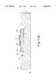
- FIG. 1(a)-(b)are cross-sectional views of a multi-chip module at various progressive stages of a procedure for using a protective layer to provide mechanical support for an air bridge structure in micro-electronic circuitry;
- FIG. 2is a cross-sectional view of a chip with an air bridge structure encased with a protective layer to provide mechanical support during processing.
- a multichip module 10has a substrate 11 with a plurality of chip cavities 11a formed therein, through a top surface 11b thereof.
- An integrated circuit chip 12 or another electronic componentis disposed in each chipwell 11a.
- Electronic components 12may be bonded to the substrate 11 with a layer of a thermoplastic adhesive 14; these electronic components 12 have contact pads 12a on an upper contact surface 12b thereof.
- These electronic components 12also have sensitive structures, such as air bridges 12c, on upper surface 12b.
- a protective layer 16is applied over and around the sensitive structure 12c creating an encapsulating volume 16v, as shown in FIG. 2.
- This encapsulating volume 16vincludes the area comprising the protective layer 16 as defined by a top surface 16a, walls 16b and a bottom 12b, as well as the area 16c underneath the air bridge which is essentially devoid of protective layer 16.
- This encapsulation volume 16vhas (1) a lower surface defined by the substrate surface plane, or the chip surface 12b, (2) an upper surface 16a spaced a distance above said sensitive structure (approximately less than 2 to 3 times the sensitive structure's height which is about 2 to about 3 microns), and (3) walls 16b which generally extend from the lower surface to the upper surface.
- the walls 16bmay have a cut (not shown) made by the mask used during deposition.
- This protective layer 16creates a protective "shield" structure covering the sensitive structure from the top and sides.
- the protective layer 16may be applied by masking the entire surface of the substrate surface 11b except the sensitive structure 12c, such that the protective layer 16 is only applied to the sensitive structure 12c.
- the entire substrate surface 11bmay be coated with the protective layer 16 and then the protective layer 16 can be removed everywhere except over the sensitive structure 12c.
- the protective layer 16is generally comprised of a carbon film which is a dielectric, and preferably is a plasma-decomposed, amorphous hydrogenated carbon byproduct of a simple hydrocarbon having 1 to 5 carbons.
- a simple hydrocarbonshould be understood to mean any material that has a boiling point below 100° C. Any commercially available hydrocarbons that become volatile below this temperature may be used, e.g., methane, propane, etc., aldehydes, alcohols, or others.
- a preferable hydrocarbonis butanone.
- This amorphous carbon film 16is preferably from about 4 to about 6 microns thick.
- the protective layer 16is produced by allowing a hydrocarbon, such as butanone liquid, to volatilize into a chamber of a reactive ion etcher/deposition system, while maintaining a reduced pressure sufficient to ignite and sustain a uniform discharge. Adhesion, density and other film characteristics may be adjusted by varying the deposition conditions. For example, a preferred method for depositing the amorphous carbon film involves a three step process. The first layer is a thin layer of dense/hard carbon for improved adhesion to the sensitive substrate and chip surface. The second layer is a thick layer of bulk amorphous carbon, followed by another layer of dense/hard carbon for maximum protection. Changing the density and thickness of the films is done by adjustment of the time and pressure settings within the deposition apparatus.
- a hydrocarbonsuch as butanone liquid
- a primer layer of known plasma-deposited adhesion-promoter materialsmay be applied.
- a preferred materialis silicon nitride.
- the thickness of this primer layermay range from 300 to 1000 angstroms. This adhesion-promoter layer also must not detrimentally affect the performance characteristics of the air bridge structure in any significant manner.
- the deposition process of either the primer layer or the dielectric protective filmis line-of-sight, they will not significantly intrude under the air bridge, and therefore will not significantly affect the performance characteristics of the air bridge.
- the film's dielectric constantis such that it should not significantly interfere with the functioning of the air bridge.
- a first stratum 18 of the overlying high density interconnect structure 17comprises a dielectric layer 20 supporting a patterned metallization layer 22.
- the dielectric layer 20has separate lower and upper sublayers 24 and 26, respectively, and supports the patterned metallization layer 22 which makes electrical contact with contact pads 12b on the substrate 11 within via holes 27 in the dielectric layer 20.
- the lower dielectric sublayer 24is a thermoplastic adhesive which allows subsequent processing at temperatures below 260° C.
- U.S. application Ser. No. 07/987,849teaches a plasticized polyetherimide adhesive, such as "Ultem”/"Benzoflex" (Ultem is a trademark of General Electric Co, Pittsfield, Mass., for a polyetherimide resin, and Benzoflex is a trademark of Velsicol Chemical Corp., Rosemont, Ill., for pentaerythritol tetrabenzoate).
- the upper dielectric sublayer 26is preferably a thermoset material (for example, a KAPTON® film). Other materials, including thermoplastics which exhibit sufficient stability, may also be used for the upper dielectric sublayer 26.
- a second stratum 28 of the high density interconnect structurecomprises a second dielectric layer 30 supporting a second patterned metallization layer 32.
- the dielectric layer 30has separate lower and upper sublayers 34 and 36, respectively.
- the second lower sublayer 34may be a siloxane polyimide/epoxy (SPIE) adhesive system as described in commonly assigned U.S. Pat. No. 5,161,093, issued Nov. 3, 1992, to Gorczyca et al, which is herein incorporated by reference in its entirety. Since this second dielectric layer is a SPIE thermosetting copolymer, and therefore changes its glass transition temperature value upon curing, laminating multiple layers (at 190° C.) does not affect lower layers.
- SPIEsiloxane polyimide/epoxy
- Via holes 37are drilled and another patterned metallization sublayer 32 extends into via holes 37 in the dielectric layer 30 to make electrical contact with the first metallization layer 22. If desired, selected via holes may extend through the first dielectric layer 20 as well to provide direct electrical contact to selected contact pads 12a.
- the third stratum 40 of the high density interconnect structurecomprises a third dielectric layer 42 supporting a third patterned metallization layer 44.
- the dielectric layer 42has separate lower and upper sublayers 46 and 48, respectively.
- the third lower dielectric sublayeris preferably a siloxane polyimide/epoxy (SPIE) adhesive.
- the third stratumalso comprises a third patterned metallization layer 44.
- the third upper dielectric sublayer 48may again be a thermoset material or a thermoplastic material and is preferably a thermoset material, i.e.,KAPTON® film. Lamination of this third stratum 40 is followed by via drilling which extends vias 49 through the stratum 40 such that the patterned metallization layer 44 will make electrical contact to the metal layer 32 of the second dielectric layer 28.
- the dielectric layers of the high density interconnect structure 17 of the present inventionmust be laser ablatable or should be rendered laser ablatable in accordance with U.S. patent application Ser. No. 456,421, entitled, “Laser Ablatable Polymer Dielectrics and Methods,” herein incorporated by reference in its entirety.
- Additional (fourth, fifth, sixth, etc.) strata of the high density interconnect structure 17are not shown in FIG. 1(b), but, if used, will be essentially identical to the lower strata 28 and 40.
- Each additional upper stratumwould comprise a dielectric layer having a thermosetting adhesive (preferably a SPIE blend) and having via holes therein, and a patterned metallization layer making electrical contact with the patterned metallization of the next lower patterned metallization layer through the via holes.
- Other stratacan be added in accordance with the above description.
- the SPIE crosslinking copolymer blend adhesive materials used as the lower dielectric sublayer in the second and higher strataare selected so that these adhesive materials become set at a low enough temperature that curing the adhesive materials has no adverse effect on the high density interconnect structure or the electronic components being connected thereby. Correct selection of the curing properties of the adhesive materials allows the structure to be fabricated and, if need be, disassembled and reassembled without an adverse effect on the electronic components being interconnected.
- the protective material 16need not be removed from below the high density interconnect structure, there is no need to use any form of removal process for HDI structure 17 to expose layer 16; thus, neither chemical etch nor laser ablation of the high density interconnect structure 17 is necessary. More importantly, there are no limitations placed on the routing of the metallization layers and the air bridge structure is not exposed to any of the conventional high density interconnect structure removal processes, such as laser ablation and plasma-ashing. This is a significant advantage in producing a highly reliable module.
- the fabricated modulemay be complete; various metallization layers 22, 32, 44 will carry power, ground, and at least one set of signal conductors. And since none of the high density interconnect structure is removed, there are few limitations on how the metallization layers must be routed.
- a GaAs chip containing air bridgeswas attached to a substrate using a thermoplastic adhesive.
- the entire assemblywas then cleaned by soaking the part for 5 minutes each in methylene chloride, acetone and propanol.
- the partwas then vacuum baked at 250° C. for 30 minutes and plasma cleaned in a barrel etcher using oxygen (150 W, 110° C., 30 min.).
- 600 ⁇ of plasma enhanced chemical vapor deposited (PECVD) silicon nitride layer (adhesion promoter)was conformably coated over the chip surface.
- PECVDplasma enhanced chemical vapor deposited
- the protective amorphous carbon structurewas then deposited, using a three-step process, in a parallel plate reactive ion etching system using 2-butanone as the hydrocarbon source.
- the first layer in the three layer processis a 500 ⁇ of hard diamond like carbon (30 mtorr, 50 W, 250 ⁇ /min.).
- the second layerwas 4 microns of soft amorphous hydrogenated carbon (500 mtorr, 50 W, 450 ⁇ /min.).
- the third layeris identical to the first layer (30 mtorr, 50 W, 250 ⁇ /min.).
- the completed protective film, comprising the three sublayerswas then patterned and removed from the test pads using laser ablation and plasma etching. The entire assembly was then laminated at 260° C. with a dielectric containing two sublayers.
- the lower sublayerwas a thermoplastic adhesive, such as "Ultem”/"Benzoflex” adhesive.
- the upper sublayer of the dielectricwas "Kapton® polyimide. After lamination the dielectric was laser ablated to expose the test probe pads.
- the GaAs chipwas then retested for electrical performance.
- the mean RF performance loss recorded at 3 to 6 GHzwas within the measurement error of the test. This indicated that the air bridge structures were not damaged by the lamination process, and the presence of the protective layer did not significantly change the chip performance.
Landscapes
- Engineering & Computer Science (AREA)
- Computer Hardware Design (AREA)
- Microelectronics & Electronic Packaging (AREA)
- Power Engineering (AREA)
- Physics & Mathematics (AREA)
- Condensed Matter Physics & Semiconductors (AREA)
- General Physics & Mathematics (AREA)
- Internal Circuitry In Semiconductor Integrated Circuit Devices (AREA)
Abstract
Description
Claims (11)
Priority Applications (1)
| Application Number | Priority Date | Filing Date | Title |
|---|---|---|---|
| US08/308,886US5524339A (en) | 1994-09-19 | 1994-09-19 | Method for protecting gallium arsenide mmic air bridge structures |
Applications Claiming Priority (1)
| Application Number | Priority Date | Filing Date | Title |
|---|---|---|---|
| US08/308,886US5524339A (en) | 1994-09-19 | 1994-09-19 | Method for protecting gallium arsenide mmic air bridge structures |
Publications (1)
| Publication Number | Publication Date |
|---|---|
| US5524339Atrue US5524339A (en) | 1996-06-11 |
Family
ID=23195795
Family Applications (1)
| Application Number | Title | Priority Date | Filing Date |
|---|---|---|---|
| US08/308,886Expired - LifetimeUS5524339A (en) | 1994-09-19 | 1994-09-19 | Method for protecting gallium arsenide mmic air bridge structures |
Country Status (1)
| Country | Link |
|---|---|
| US (1) | US5524339A (en) |
Cited By (63)
| Publication number | Priority date | Publication date | Assignee | Title |
|---|---|---|---|---|
| US5567657A (en)* | 1995-12-04 | 1996-10-22 | General Electric Company | Fabrication and structures of two-sided molded circuit modules with flexible interconnect layers |
| US5672546A (en)* | 1995-12-04 | 1997-09-30 | General Electric Company | Semiconductor interconnect method and structure for high temperature applications |
| US5757072A (en)* | 1994-12-19 | 1998-05-26 | Martin Marietta Corporation | Structure for protecting air bridges on semiconductor chips from damage |
| US5841075A (en)* | 1996-11-08 | 1998-11-24 | W. L. Gore & Associates, Inc. | Method for reducing via inductance in an electronic assembly and article |
| EP0895285A3 (en)* | 1997-07-28 | 1999-05-12 | General Electric Company | Amorphous hydrogenated carbon hermetic structure and fabrication method |
| US5943598A (en)* | 1995-10-19 | 1999-08-24 | Stmicroelectronics, Inc. | Integrated circuit with planarized dielectric layer between successive polysilicon layers |
| US5966633A (en)* | 1995-03-17 | 1999-10-12 | International Business Machines Corporation | Method for providing a metallization layer on an insulating layer and for opening through holes in the said insulating layer using the same mask |
| US5973908A (en)* | 1995-12-04 | 1999-10-26 | General Electric Company | Structure for thin film capacitors |
| US6001673A (en)* | 1999-02-11 | 1999-12-14 | Ericsson Inc. | Methods for packaging integrated circuit devices including cavities adjacent active regions |
| US6020252A (en)* | 1996-05-15 | 2000-02-01 | Commissariat A L'energie Atomique | Method of producing a thin layer of semiconductor material |
| US6081988A (en)* | 1998-04-30 | 2000-07-04 | Lockheed Martin Corp. | Fabrication of a circuit module with a coaxial transmission line |
| US6081989A (en)* | 1998-04-30 | 2000-07-04 | Lockheed Martin Corporation | Fabrication of circuit modules with a transmission line |
| US6229203B1 (en)* | 1997-03-12 | 2001-05-08 | General Electric Company | Semiconductor interconnect structure for high temperature applications |
| US6256875B1 (en)* | 1996-03-28 | 2001-07-10 | Mitsubishi Denki Kabushiki Kaisha | Method for manufacturing semiconductor device |
| US6423566B1 (en)* | 1998-07-24 | 2002-07-23 | International Business Machines Corporation | Moisture and ion barrier for protection of devices and interconnect structures |
| US20020175402A1 (en)* | 2001-05-23 | 2002-11-28 | Mccormack Mark Thomas | Structure and method of embedding components in multi-layer substrates |
| US20030077885A1 (en)* | 2000-05-30 | 2003-04-24 | Bernard Aspar | Embrittled substrate and method for making same |
| WO2003041163A1 (en)* | 2001-11-09 | 2003-05-15 | 3D Plus | Device for the hermetic encapsulation of a component that must be protected against all stresses |
| US20030102547A1 (en)* | 1999-12-16 | 2003-06-05 | Mitsutoshi Higashi | Semiconductor device and production method thereof |
| US6581279B1 (en)* | 1998-08-25 | 2003-06-24 | Commissariat A L'energie Atomique | Method of collectively packaging electronic components |
| US20030122244A1 (en)* | 2001-12-31 | 2003-07-03 | Mou-Shiung Lin | Integrated chip package structure using metal substrate and method of manufacturing the same |
| US20030168250A1 (en)* | 2002-02-22 | 2003-09-11 | Bridgewave Communications, Inc. | High frequency device packages and methods |
| US20030189246A1 (en)* | 2002-04-03 | 2003-10-09 | Matsushita Electric Industrial Co., Ltd. | Semiconductor built -in millimeter-wave band module |
| US20030201521A1 (en)* | 2002-04-25 | 2003-10-30 | Macronix International Co., Ltd. | Semiconductor packaging device and manufacture thereof |
| US20040058474A1 (en)* | 2002-09-25 | 2004-03-25 | International Business Machines Corporation | Semiconductor chip module and method of manufacture of same |
| US20040135269A1 (en)* | 2002-07-23 | 2004-07-15 | Seiko Epson Corporation | Interconnect substrate, semiconductor device, methods of manufacturing the same, circuit board, and electronic equipment |
| US20050017271A1 (en)* | 1999-03-11 | 2005-01-27 | Shinko Electric Industries Co.,Inc. | Multilayered substrate for semiconductor device and method of manufacturing same |
| US20050116337A1 (en)* | 2002-08-27 | 2005-06-02 | Swee Kwang Chua | Method of making multichip wafer level packages and computing systems incorporating same |
| US6938783B2 (en)* | 2000-07-26 | 2005-09-06 | Amerasia International Technology, Inc. | Carrier tape |
| US20060099733A1 (en)* | 2004-11-09 | 2006-05-11 | Geefay Frank S | Semiconductor package and fabrication method |
| US20080151522A1 (en)* | 2000-09-25 | 2008-06-26 | Ibiden Co., Ltd. | Semiconductor element, method of manufacturing semiconductor element, multi-layer printed circuit board, and method of manufacturing multi-layer printed circuit board |
| US20080201944A1 (en)* | 2000-02-25 | 2008-08-28 | Ibiden Co., Ltd. | Multilayer printed circuit board and multilayer printed circuit board manufacturing method |
| US20080237780A1 (en)* | 2007-03-26 | 2008-10-02 | Semiconductor Energy Laboratory Co., Ltd. | SOI substrate and method for manufacturing SOI substrate |
| US20080237779A1 (en)* | 2007-03-26 | 2008-10-02 | Semiconductor Energy Laboratory Co., Ltd. | SOI substrate and method for manufacturing SOI substrate |
| US20080248382A1 (en)* | 2007-03-30 | 2008-10-09 | The Regents Of The University Of Michigan | Deposited Microarchitectured Battery and Manufacturing Method |
| US20080254560A1 (en)* | 2007-04-13 | 2008-10-16 | Semiconductor Energy Laboratory Co., Ltd. | Display device, method for manufacturing display device, and SOI substrate |
| US20090011542A1 (en)* | 2001-03-30 | 2009-01-08 | Megica Corporation | Structure and manufactruing method of chip scale package |
| US20090120568A1 (en)* | 2005-08-16 | 2009-05-14 | Chrystel Deguet | Method of transferring a thin film onto a support |
| US20090156016A1 (en)* | 2007-12-17 | 2009-06-18 | Lea Di Cioccio | Method for transfer of a thin layer |
| US20100167499A1 (en)* | 2002-12-09 | 2010-07-01 | Commissariat A L'energie Atomique | Method for making a stressed structure designed to be dissociated |
| US7883994B2 (en) | 1997-12-30 | 2011-02-08 | Commissariat A L'energie Atomique | Process for the transfer of a thin film |
| US7902038B2 (en) | 2001-04-13 | 2011-03-08 | Commissariat A L'energie Atomique | Detachable substrate with controlled mechanical strength and method of producing same |
| US20110117705A1 (en)* | 2009-11-15 | 2011-05-19 | Microsemi Corporation | Multi-layer thick-film rf package |
| US20110116237A1 (en)* | 2009-11-15 | 2011-05-19 | Microsemi Corporation | Rf package |
| US8048766B2 (en) | 2003-06-24 | 2011-11-01 | Commissariat A L'energie Atomique | Integrated circuit on high performance chip |
| US8193069B2 (en) | 2003-07-21 | 2012-06-05 | Commissariat A L'energie Atomique | Stacked structure and production method thereof |
| US8252663B2 (en) | 2009-06-18 | 2012-08-28 | Commissariat A L'energie Atomique Et Aux Energies Alternatives | Method of transferring a thin layer onto a target substrate having a coefficient of thermal expansion different from that of the thin layer |
| US20120228755A1 (en)* | 2011-03-08 | 2012-09-13 | Kabushiki Kaisha Toshiba | Semiconductor module and manufacturing method thereof |
| US8309431B2 (en) | 2003-10-28 | 2012-11-13 | Commissariat A L'energie Atomique | Method for self-supported transfer of a fine layer by pulsation after implantation or co-implantation |
| US8471361B2 (en) | 2001-12-31 | 2013-06-25 | Megica Corporation | Integrated chip package structure using organic substrate and method of manufacturing the same |
| US8492870B2 (en) | 2002-01-19 | 2013-07-23 | Megica Corporation | Semiconductor package with interconnect layers |
| US8535976B2 (en) | 2001-12-31 | 2013-09-17 | Megica Corporation | Method for fabricating chip package with die and substrate |
| US8581113B2 (en) | 2007-12-19 | 2013-11-12 | Bridgewave Communications, Inc. | Low cost high frequency device package and methods |
| US8581406B1 (en)* | 2012-04-20 | 2013-11-12 | Raytheon Company | Flip chip mounted monolithic microwave integrated circuit (MMIC) structure |
| US8664084B2 (en) | 2005-09-28 | 2014-03-04 | Commissariat A L'energie Atomique | Method for making a thin-film element |
| US8778775B2 (en) | 2006-12-19 | 2014-07-15 | Commissariat A L'energie Atomique | Method for preparing thin GaN layers by implantation and recycling of a starting substrate |
| US20150061124A1 (en)* | 2007-12-14 | 2015-03-05 | Stats Chippac, Ltd. | Semiconductor Device and Method of Forming Interconnect Structure for Encapsulated Die Having Pre-Applied Protective Layer |
| US9030029B2 (en)* | 2001-12-31 | 2015-05-12 | Qualcomm Incorporated | Chip package with die and substrate |
| US20150380369A1 (en)* | 2013-09-30 | 2015-12-31 | Nantong Fujitsu Microelectronics Co., Ltd | Wafer packaging structure and packaging method |
| US9666500B2 (en) | 2007-12-14 | 2017-05-30 | STATS ChipPAC Pte. Ltd. | Semiconductor device and method of forming insulating layer disposed over the semiconductor die for stress relief |
| WO2018200304A1 (en)* | 2017-04-26 | 2018-11-01 | General Electric Company | Ultrasound probe with thin film flex circuit and methods of providing same |
| US10204866B2 (en) | 2010-03-12 | 2019-02-12 | STATS ChipPAC Pte. Ltd. | Semiconductor device and method of forming sacrificial protective layer to protect semiconductor die edge during singulation |
| US10998248B2 (en) | 2007-12-14 | 2021-05-04 | JCET Semiconductor (Shaoxing) Co. Ltd. | Semiconductor device and method of forming sacrificial adhesive over contact pads of semiconductor die |
Citations (18)
| Publication number | Priority date | Publication date | Assignee | Title |
|---|---|---|---|---|
| US4217684A (en)* | 1979-04-16 | 1980-08-19 | General Electric Company | Fabrication of front surface matched ultrasonic transducer array |
| US4631820A (en)* | 1984-08-23 | 1986-12-30 | Canon Kabushiki Kaisha | Mounting assembly and mounting method for an electronic component |
| US4725924A (en)* | 1985-04-10 | 1988-02-16 | Em Microelectronic-Marin Sa | Electronic unit especially for microcircuit cards and card comprising such a unit |
| US4783695A (en)* | 1986-09-26 | 1988-11-08 | General Electric Company | Multichip integrated circuit packaging configuration and method |
| US4835704A (en)* | 1986-12-29 | 1989-05-30 | General Electric Company | Adaptive lithography system to provide high density interconnect |
| US4878991A (en)* | 1988-12-12 | 1989-11-07 | General Electric Company | Simplified method for repair of high density interconnect circuits |
| US4894115A (en)* | 1989-02-14 | 1990-01-16 | General Electric Company | Laser beam scanning method for forming via holes in polymer materials |
| US4918811A (en)* | 1986-09-26 | 1990-04-24 | General Electric Company | Multichip integrated circuit packaging method |
| US4933042A (en)* | 1986-09-26 | 1990-06-12 | General Electric Company | Method for packaging integrated circuit chips employing a polymer film overlay layer |
| US5158911A (en)* | 1990-08-03 | 1992-10-27 | Thomson Composants Microondes | Method for interconnection between an integrated circuit and a support circuit, and integrated circuit adapted to this method |
| US5161093A (en)* | 1990-07-02 | 1992-11-03 | General Electric Company | Multiple lamination high density interconnect process and structure employing a variable crosslinking adhesive |
| US5255431A (en)* | 1992-06-26 | 1993-10-26 | General Electric Company | Method of using frozen epoxy for placing pin-mounted components in a circuit module |
| US5306670A (en)* | 1993-02-09 | 1994-04-26 | Texas Instruments Incorporated | Multi-chip integrated circuit module and method for fabrication thereof |
| US5323533A (en)* | 1991-03-26 | 1994-06-28 | Thomson-Csf | Method of producing coaxial connections for an electronic component, and component package |
| US5324687A (en)* | 1992-10-16 | 1994-06-28 | General Electric Company | Method for thinning of integrated circuit chips for lightweight packaged electronic systems |
| US5331203A (en)* | 1990-04-05 | 1994-07-19 | General Electric Company | High density interconnect structure including a chamber |
| US5338975A (en)* | 1990-07-02 | 1994-08-16 | General Electric Company | High density interconnect structure including a spacer structure and a gap |
| US5353498A (en)* | 1993-02-08 | 1994-10-11 | General Electric Company | Method for fabricating an integrated circuit module |
- 1994
- 1994-09-19USUS08/308,886patent/US5524339A/ennot_activeExpired - Lifetime
Patent Citations (18)
| Publication number | Priority date | Publication date | Assignee | Title |
|---|---|---|---|---|
| US4217684A (en)* | 1979-04-16 | 1980-08-19 | General Electric Company | Fabrication of front surface matched ultrasonic transducer array |
| US4631820A (en)* | 1984-08-23 | 1986-12-30 | Canon Kabushiki Kaisha | Mounting assembly and mounting method for an electronic component |
| US4725924A (en)* | 1985-04-10 | 1988-02-16 | Em Microelectronic-Marin Sa | Electronic unit especially for microcircuit cards and card comprising such a unit |
| US4918811A (en)* | 1986-09-26 | 1990-04-24 | General Electric Company | Multichip integrated circuit packaging method |
| US4783695A (en)* | 1986-09-26 | 1988-11-08 | General Electric Company | Multichip integrated circuit packaging configuration and method |
| US4933042A (en)* | 1986-09-26 | 1990-06-12 | General Electric Company | Method for packaging integrated circuit chips employing a polymer film overlay layer |
| US4835704A (en)* | 1986-12-29 | 1989-05-30 | General Electric Company | Adaptive lithography system to provide high density interconnect |
| US4878991A (en)* | 1988-12-12 | 1989-11-07 | General Electric Company | Simplified method for repair of high density interconnect circuits |
| US4894115A (en)* | 1989-02-14 | 1990-01-16 | General Electric Company | Laser beam scanning method for forming via holes in polymer materials |
| US5331203A (en)* | 1990-04-05 | 1994-07-19 | General Electric Company | High density interconnect structure including a chamber |
| US5161093A (en)* | 1990-07-02 | 1992-11-03 | General Electric Company | Multiple lamination high density interconnect process and structure employing a variable crosslinking adhesive |
| US5338975A (en)* | 1990-07-02 | 1994-08-16 | General Electric Company | High density interconnect structure including a spacer structure and a gap |
| US5158911A (en)* | 1990-08-03 | 1992-10-27 | Thomson Composants Microondes | Method for interconnection between an integrated circuit and a support circuit, and integrated circuit adapted to this method |
| US5323533A (en)* | 1991-03-26 | 1994-06-28 | Thomson-Csf | Method of producing coaxial connections for an electronic component, and component package |
| US5255431A (en)* | 1992-06-26 | 1993-10-26 | General Electric Company | Method of using frozen epoxy for placing pin-mounted components in a circuit module |
| US5324687A (en)* | 1992-10-16 | 1994-06-28 | General Electric Company | Method for thinning of integrated circuit chips for lightweight packaged electronic systems |
| US5353498A (en)* | 1993-02-08 | 1994-10-11 | General Electric Company | Method for fabricating an integrated circuit module |
| US5306670A (en)* | 1993-02-09 | 1994-04-26 | Texas Instruments Incorporated | Multi-chip integrated circuit module and method for fabrication thereof |
Cited By (141)
| Publication number | Priority date | Publication date | Assignee | Title |
|---|---|---|---|---|
| US5757072A (en)* | 1994-12-19 | 1998-05-26 | Martin Marietta Corporation | Structure for protecting air bridges on semiconductor chips from damage |
| US5966633A (en)* | 1995-03-17 | 1999-10-12 | International Business Machines Corporation | Method for providing a metallization layer on an insulating layer and for opening through holes in the said insulating layer using the same mask |
| US5943598A (en)* | 1995-10-19 | 1999-08-24 | Stmicroelectronics, Inc. | Integrated circuit with planarized dielectric layer between successive polysilicon layers |
| US5973908A (en)* | 1995-12-04 | 1999-10-26 | General Electric Company | Structure for thin film capacitors |
| US5672546A (en)* | 1995-12-04 | 1997-09-30 | General Electric Company | Semiconductor interconnect method and structure for high temperature applications |
| US5567657A (en)* | 1995-12-04 | 1996-10-22 | General Electric Company | Fabrication and structures of two-sided molded circuit modules with flexible interconnect layers |
| US5949133A (en)* | 1995-12-04 | 1999-09-07 | General Electric Company | Semiconductor interconnect structure for high temperature applications |
| US6256875B1 (en)* | 1996-03-28 | 2001-07-10 | Mitsubishi Denki Kabushiki Kaisha | Method for manufacturing semiconductor device |
| US8101503B2 (en) | 1996-05-15 | 2012-01-24 | Commissariat A L'energie Atomique | Method of producing a thin layer of semiconductor material |
| US6809009B2 (en) | 1996-05-15 | 2004-10-26 | Commissariat A L'energie Atomique | Method of producing a thin layer of semiconductor material |
| US6020252A (en)* | 1996-05-15 | 2000-02-01 | Commissariat A L'energie Atomique | Method of producing a thin layer of semiconductor material |
| US20060115961A1 (en)* | 1996-05-15 | 2006-06-01 | Bernard Aspar | Method of producing a thin layer of semiconductor material |
| US7498234B2 (en) | 1996-05-15 | 2009-03-03 | Commissariat A L'energie Atomique | Method of producing a thin layer of semiconductor material |
| US7067396B2 (en) | 1996-05-15 | 2006-06-27 | Commissariat A L'energie Atomique | Method of producing a thin layer of semiconductor material |
| US6225192B1 (en) | 1996-05-15 | 2001-05-01 | Commissariat A L'energie Atomique | Method of producing a thin layer of semiconductor material |
| US6021564A (en)* | 1996-11-08 | 2000-02-08 | W. L. Gore & Associates, Inc. | Method for reducing via inductance in an electronic assembly and article |
| US5841075A (en)* | 1996-11-08 | 1998-11-24 | W. L. Gore & Associates, Inc. | Method for reducing via inductance in an electronic assembly and article |
| US6229203B1 (en)* | 1997-03-12 | 2001-05-08 | General Electric Company | Semiconductor interconnect structure for high temperature applications |
| US6150719A (en)* | 1997-07-28 | 2000-11-21 | General Electric Company | Amorphous hydrogenated carbon hermetic structure and fabrication method |
| US6548329B1 (en) | 1997-07-28 | 2003-04-15 | General Electric Company | Amorphous hydrogenated carbon hermetic structure fabrication method |
| EP0895285A3 (en)* | 1997-07-28 | 1999-05-12 | General Electric Company | Amorphous hydrogenated carbon hermetic structure and fabrication method |
| US8609514B2 (en) | 1997-12-10 | 2013-12-17 | Commissariat A L'energie Atomique | Process for the transfer of a thin film comprising an inclusion creation step |
| US8470712B2 (en) | 1997-12-30 | 2013-06-25 | Commissariat A L'energie Atomique | Process for the transfer of a thin film comprising an inclusion creation step |
| US20110092051A1 (en)* | 1997-12-30 | 2011-04-21 | Commissariat A L'energie Atomique | Process for the transfer of a thin film comprising an inclusion creation step |
| US7883994B2 (en) | 1997-12-30 | 2011-02-08 | Commissariat A L'energie Atomique | Process for the transfer of a thin film |
| US6465730B1 (en)* | 1998-04-30 | 2002-10-15 | Lockhead Martin Corporation | Fabrication of a circuit module with a coaxial transmission line |
| US6081989A (en)* | 1998-04-30 | 2000-07-04 | Lockheed Martin Corporation | Fabrication of circuit modules with a transmission line |
| US6081988A (en)* | 1998-04-30 | 2000-07-04 | Lockheed Martin Corp. | Fabrication of a circuit module with a coaxial transmission line |
| US6423566B1 (en)* | 1998-07-24 | 2002-07-23 | International Business Machines Corporation | Moisture and ion barrier for protection of devices and interconnect structures |
| US6581279B1 (en)* | 1998-08-25 | 2003-06-24 | Commissariat A L'energie Atomique | Method of collectively packaging electronic components |
| US6001673A (en)* | 1999-02-11 | 1999-12-14 | Ericsson Inc. | Methods for packaging integrated circuit devices including cavities adjacent active regions |
| US7763809B2 (en)* | 1999-03-11 | 2010-07-27 | Shink Electric Industries Co., Inc. | Multilayered substrate for semiconductor device and method of manufacturing same |
| US20050017271A1 (en)* | 1999-03-11 | 2005-01-27 | Shinko Electric Industries Co.,Inc. | Multilayered substrate for semiconductor device and method of manufacturing same |
| US20030102547A1 (en)* | 1999-12-16 | 2003-06-05 | Mitsutoshi Higashi | Semiconductor device and production method thereof |
| US6861284B2 (en)* | 1999-12-16 | 2005-03-01 | Shinko Electric Industries Co., Ltd. | Semiconductor device and production method thereof |
| US8453323B2 (en)* | 2000-02-25 | 2013-06-04 | Ibiden Co., Ltd. | Printed circuit board manufacturing method |
| US20080201944A1 (en)* | 2000-02-25 | 2008-08-28 | Ibiden Co., Ltd. | Multilayer printed circuit board and multilayer printed circuit board manufacturing method |
| US8186045B2 (en) | 2000-02-25 | 2012-05-29 | Ibiden Co., Ltd. | Multilayer printed circuit board and multilayer printed circuit board manufacturing method |
| US20120000068A1 (en)* | 2000-02-25 | 2012-01-05 | Ibiden Co., Ltd. | Printed circuit board manufacturing method |
| US20100031503A1 (en)* | 2000-02-25 | 2010-02-11 | Ibiden Co., Ltd. | Multilayer printed circuit board and multilayer printed circuit board manufacturing method |
| US20100018049A1 (en)* | 2000-02-25 | 2010-01-28 | Ibiden Co., Ltd. | Multilayer printed circuit board and multilayer printed circuit board manufacturing method |
| US8438727B2 (en)* | 2000-02-25 | 2013-05-14 | Ibiden Co., Ltd. | Multilayer printed circuit board and multilayer printed circuit board manufacturing method |
| US8079142B2 (en)* | 2000-02-25 | 2011-12-20 | Ibiden Co., Ltd. | Printed circuit board manufacturing method |
| US8046914B2 (en) | 2000-02-25 | 2011-11-01 | Ibiden Co., Ltd. | Method for manufacturing multilayer printed circuit board |
| US20090070996A1 (en)* | 2000-02-25 | 2009-03-19 | Ibiden Co., Ltd. | Printed circuit board manufacturing method |
| US20030077885A1 (en)* | 2000-05-30 | 2003-04-24 | Bernard Aspar | Embrittled substrate and method for making same |
| US7498245B2 (en)* | 2000-05-30 | 2009-03-03 | Commissariat A L'energie Atomique | Embrittled substrate and method for making same |
| US6938783B2 (en)* | 2000-07-26 | 2005-09-06 | Amerasia International Technology, Inc. | Carrier tape |
| US20090263939A1 (en)* | 2000-09-25 | 2009-10-22 | Ibiden Co., Ltd. | Semiconductor element, method of manufacturing semiconductor element, multi-layer printed circuit board, and method of manufacturing multi-layer printed circuit board |
| US20090077796A1 (en)* | 2000-09-25 | 2009-03-26 | Ibiden Co., Ltd. | Semiconductor element, method of manufacturing semiconductor element, multi-layer printed circuit board, and method of manufacturing multi-layer printed circuit board |
| US8293579B2 (en) | 2000-09-25 | 2012-10-23 | Ibiden Co., Ltd. | Semiconductor element, method of manufacturing semiconductor element, multi-layer printed circuit board, and method of manufacturing multi-layer printed circuit board |
| US20080206926A1 (en)* | 2000-09-25 | 2008-08-28 | Ibiden Co., Ltd. | Semiconductor element, method of manufacturing semiconductor element, multi-layer printed circuit board, and method of manufacturing multi-layer printed circuit board |
| US8067699B2 (en) | 2000-09-25 | 2011-11-29 | Ibiden Co., Ltd. | Semiconductor element, method of manufacturing semiconductor element, multi-layer printed circuit board, and method of manufacturing multi-layer printed circuit board |
| US9245838B2 (en) | 2000-09-25 | 2016-01-26 | Ibiden Co., Ltd. | Semiconductor element |
| US8524535B2 (en) | 2000-09-25 | 2013-09-03 | Ibiden Co., Ltd. | Semiconductor element, method of manufacturing semiconductor element, multi-layer printed circuit board, and method of manufacturing multi-layer printed circuit board |
| US20100140803A1 (en)* | 2000-09-25 | 2010-06-10 | Ibiden Co., Ltd. | Semiconductor element, method of manufacturing semiconductor element, multi-layer printed circuit board, and method of manufacturing multi-layer printed circuit board |
| US20080151522A1 (en)* | 2000-09-25 | 2008-06-26 | Ibiden Co., Ltd. | Semiconductor element, method of manufacturing semiconductor element, multi-layer printed circuit board, and method of manufacturing multi-layer printed circuit board |
| US8959756B2 (en) | 2000-09-25 | 2015-02-24 | Ibiden Co., Ltd. | Method of manufacturing a printed circuit board having an embedded electronic component |
| US8822323B2 (en) | 2000-09-25 | 2014-09-02 | Ibiden Co., Ltd. | Semiconductor element, method of manufacturing semiconductor element, multi-layer printed circuit board, and method of manufacturing multi-layer printed circuit board |
| US20090011542A1 (en)* | 2001-03-30 | 2009-01-08 | Megica Corporation | Structure and manufactruing method of chip scale package |
| US20090289346A1 (en)* | 2001-03-30 | 2009-11-26 | Megica Corporation | Structure and manufacturing method of chip scale package |
| US8426982B2 (en) | 2001-03-30 | 2013-04-23 | Megica Corporation | Structure and manufacturing method of chip scale package |
| US8912666B2 (en) | 2001-03-30 | 2014-12-16 | Qualcomm Incorporated | Structure and manufacturing method of chip scale package |
| US9018774B2 (en) | 2001-03-30 | 2015-04-28 | Qualcomm Incorporated | Chip package |
| US8748227B2 (en) | 2001-03-30 | 2014-06-10 | Megit Acquisition Corp. | Method of fabricating chip package |
| US7902038B2 (en) | 2001-04-13 | 2011-03-08 | Commissariat A L'energie Atomique | Detachable substrate with controlled mechanical strength and method of producing same |
| US20020175402A1 (en)* | 2001-05-23 | 2002-11-28 | Mccormack Mark Thomas | Structure and method of embedding components in multi-layer substrates |
| FR2832136A1 (en)* | 2001-11-09 | 2003-05-16 | 3D Plus Sa | DEVICE FOR HERMETIC ENCAPSULATION OF COMPONENT TO BE PROTECTED FROM ANY STRESS |
| WO2003041163A1 (en)* | 2001-11-09 | 2003-05-15 | 3D Plus | Device for the hermetic encapsulation of a component that must be protected against all stresses |
| US20050012188A1 (en)* | 2001-11-09 | 2005-01-20 | Christian Val | Device for the hermetic encapsulation of a component that must be protected against all stresses |
| US8471361B2 (en) | 2001-12-31 | 2013-06-25 | Megica Corporation | Integrated chip package structure using organic substrate and method of manufacturing the same |
| US9136246B2 (en) | 2001-12-31 | 2015-09-15 | Qualcomm Incorporated | Integrated chip package structure using silicon substrate and method of manufacturing the same |
| US8835221B2 (en) | 2001-12-31 | 2014-09-16 | Qualcomm Incorporated | Integrated chip package structure using ceramic substrate and method of manufacturing the same |
| US9030029B2 (en)* | 2001-12-31 | 2015-05-12 | Qualcomm Incorporated | Chip package with die and substrate |
| US8535976B2 (en) | 2001-12-31 | 2013-09-17 | Megica Corporation | Method for fabricating chip package with die and substrate |
| US20030122244A1 (en)* | 2001-12-31 | 2003-07-03 | Mou-Shiung Lin | Integrated chip package structure using metal substrate and method of manufacturing the same |
| US8119446B2 (en)* | 2001-12-31 | 2012-02-21 | Megica Corporation | Integrated chip package structure using metal substrate and method of manufacturing the same |
| US8492870B2 (en) | 2002-01-19 | 2013-07-23 | Megica Corporation | Semiconductor package with interconnect layers |
| US6770822B2 (en)* | 2002-02-22 | 2004-08-03 | Bridgewave Communications, Inc. | High frequency device packages and methods |
| US7520054B2 (en) | 2002-02-22 | 2009-04-21 | Bridgewave Communications, Inc. | Process of manufacturing high frequency device packages |
| US20030168250A1 (en)* | 2002-02-22 | 2003-09-11 | Bridgewave Communications, Inc. | High frequency device packages and methods |
| US7061100B2 (en)* | 2002-04-03 | 2006-06-13 | Matsushita Electric Industrial Co., Ltd. | Semiconductor built-in millimeter-wave band module |
| US20030189246A1 (en)* | 2002-04-03 | 2003-10-09 | Matsushita Electric Industrial Co., Ltd. | Semiconductor built -in millimeter-wave band module |
| US7122904B2 (en)* | 2002-04-25 | 2006-10-17 | Macronix International Co., Ltd. | Semiconductor packaging device and manufacture thereof |
| US20070018333A1 (en)* | 2002-04-25 | 2007-01-25 | Macronix International Co., Ltd. | Semiconductor packaging device and manufacture thereof |
| US20030201521A1 (en)* | 2002-04-25 | 2003-10-30 | Macronix International Co., Ltd. | Semiconductor packaging device and manufacture thereof |
| US20040135269A1 (en)* | 2002-07-23 | 2004-07-15 | Seiko Epson Corporation | Interconnect substrate, semiconductor device, methods of manufacturing the same, circuit board, and electronic equipment |
| US20060165875A1 (en)* | 2002-07-23 | 2006-07-27 | Seiko Epson Corporation | Interconnect substrate, semiconductor device, methods of manufacturing the same, circuit board, and electronic equipment |
| US20080293239A1 (en)* | 2002-07-23 | 2008-11-27 | Seiko Epson Corporation | Interconnect substrate, semiconductor device, methods of manufacturing the same, circuit board, and electronic equipment |
| US7541278B2 (en) | 2002-07-23 | 2009-06-02 | Seiko Epson Corporation | Interconnect substrate, semiconductor device, methods of manufacturing the same, circuit board, and electronic equipment |
| US7413975B2 (en) | 2002-07-23 | 2008-08-19 | Seiko Epson Corporation | Interconnect substrate, semiconductor device, methods of manufacturing the same, circuit board, and electronic equipment |
| US20050116337A1 (en)* | 2002-08-27 | 2005-06-02 | Swee Kwang Chua | Method of making multichip wafer level packages and computing systems incorporating same |
| US7485562B2 (en)* | 2002-08-27 | 2009-02-03 | Micron Technology, Inc. | Method of making multichip wafer level packages and computing systems incorporating same |
| US6759270B2 (en)* | 2002-09-25 | 2004-07-06 | International Buisness Machines Corporation | Semiconductor chip module and method of manufacture of same |
| US20040058474A1 (en)* | 2002-09-25 | 2004-03-25 | International Business Machines Corporation | Semiconductor chip module and method of manufacture of same |
| US8389379B2 (en) | 2002-12-09 | 2013-03-05 | Commissariat A L'energie Atomique | Method for making a stressed structure designed to be dissociated |
| US20100167499A1 (en)* | 2002-12-09 | 2010-07-01 | Commissariat A L'energie Atomique | Method for making a stressed structure designed to be dissociated |
| US8048766B2 (en) | 2003-06-24 | 2011-11-01 | Commissariat A L'energie Atomique | Integrated circuit on high performance chip |
| US8193069B2 (en) | 2003-07-21 | 2012-06-05 | Commissariat A L'energie Atomique | Stacked structure and production method thereof |
| US8309431B2 (en) | 2003-10-28 | 2012-11-13 | Commissariat A L'energie Atomique | Method for self-supported transfer of a fine layer by pulsation after implantation or co-implantation |
| US20070020807A1 (en)* | 2004-11-09 | 2007-01-25 | Geefay Frank S | Protective structures and methods of fabricating protective structures over wafers |
| US20060099733A1 (en)* | 2004-11-09 | 2006-05-11 | Geefay Frank S | Semiconductor package and fabrication method |
| US20090120568A1 (en)* | 2005-08-16 | 2009-05-14 | Chrystel Deguet | Method of transferring a thin film onto a support |
| US8142593B2 (en) | 2005-08-16 | 2012-03-27 | Commissariat A L'energie Atomique | Method of transferring a thin film onto a support |
| US8664084B2 (en) | 2005-09-28 | 2014-03-04 | Commissariat A L'energie Atomique | Method for making a thin-film element |
| US8778775B2 (en) | 2006-12-19 | 2014-07-15 | Commissariat A L'energie Atomique | Method for preparing thin GaN layers by implantation and recycling of a starting substrate |
| US20080237779A1 (en)* | 2007-03-26 | 2008-10-02 | Semiconductor Energy Laboratory Co., Ltd. | SOI substrate and method for manufacturing SOI substrate |
| US20080237780A1 (en)* | 2007-03-26 | 2008-10-02 | Semiconductor Energy Laboratory Co., Ltd. | SOI substrate and method for manufacturing SOI substrate |
| US8222117B2 (en) | 2007-03-26 | 2012-07-17 | Semiconductor Energy Laboratory Co., Ltd. | SOI substrate and method for manufacturing SOI substrate |
| US9111997B2 (en) | 2007-03-26 | 2015-08-18 | Semiconductor Energy Laboratory Co., Ltd. | SOI substrate and method for manufacturing SOI substrate |
| US8101466B2 (en)* | 2007-03-26 | 2012-01-24 | Semiconductor Energy Laboratory Co., Ltd. | SOI substrate and method for manufacturing SOI substrate |
| US20080248382A1 (en)* | 2007-03-30 | 2008-10-09 | The Regents Of The University Of Michigan | Deposited Microarchitectured Battery and Manufacturing Method |
| US8603662B2 (en) | 2007-03-30 | 2013-12-10 | The Regents Of The University Of Michigan | Deposited microarchitectured battery and manufacturing method |
| US8231998B2 (en) | 2007-03-30 | 2012-07-31 | The Regents Of The University Of Michigan | Deposited microarchitectured battery and manufacturing method |
| WO2008121972A3 (en)* | 2007-03-30 | 2008-11-27 | Univ Michigan | Deposited microarchitectured battery and manufacturing method |
| US8048728B2 (en) | 2007-04-13 | 2011-11-01 | Semiconductor Energy Laboratory Co., Ltd. | Display device, method for manufacturing display device, and SOI substrate |
| US8748243B2 (en) | 2007-04-13 | 2014-06-10 | Semiconductor Energy Laboratory Co., Ltd. | Display device, method for manufacturing display device, and SOI substrate |
| US20080254560A1 (en)* | 2007-04-13 | 2008-10-16 | Semiconductor Energy Laboratory Co., Ltd. | Display device, method for manufacturing display device, and SOI substrate |
| US9559029B2 (en)* | 2007-12-14 | 2017-01-31 | STATS ChipPAC Pte. Ltd. | Semiconductor device and method of forming interconnect structure for encapsulated die having pre-applied protective layer |
| US9666500B2 (en) | 2007-12-14 | 2017-05-30 | STATS ChipPAC Pte. Ltd. | Semiconductor device and method of forming insulating layer disposed over the semiconductor die for stress relief |
| US20150061124A1 (en)* | 2007-12-14 | 2015-03-05 | Stats Chippac, Ltd. | Semiconductor Device and Method of Forming Interconnect Structure for Encapsulated Die Having Pre-Applied Protective Layer |
| US10998248B2 (en) | 2007-12-14 | 2021-05-04 | JCET Semiconductor (Shaoxing) Co. Ltd. | Semiconductor device and method of forming sacrificial adhesive over contact pads of semiconductor die |
| US7960248B2 (en) | 2007-12-17 | 2011-06-14 | Commissariat A L'energie Atomique | Method for transfer of a thin layer |
| US20090156016A1 (en)* | 2007-12-17 | 2009-06-18 | Lea Di Cioccio | Method for transfer of a thin layer |
| US9275961B2 (en) | 2007-12-19 | 2016-03-01 | Rosenberger Hochfrequenztechnik Gmbh & Co. Kg | Low cost high frequency device package and methods |
| US8839508B2 (en) | 2007-12-19 | 2014-09-23 | Rosenberger Hochfrequenztechnick GmbH & Co. KG | Method of making a high frequency device package |
| US8581113B2 (en) | 2007-12-19 | 2013-11-12 | Bridgewave Communications, Inc. | Low cost high frequency device package and methods |
| US8252663B2 (en) | 2009-06-18 | 2012-08-28 | Commissariat A L'energie Atomique Et Aux Energies Alternatives | Method of transferring a thin layer onto a target substrate having a coefficient of thermal expansion different from that of the thin layer |
| US8410601B2 (en) | 2009-11-15 | 2013-04-02 | Microsemi Corporation | RF package |
| US8034666B2 (en) | 2009-11-15 | 2011-10-11 | Microsemi Corporation | Multi-layer thick-film RF package |
| US20110117705A1 (en)* | 2009-11-15 | 2011-05-19 | Microsemi Corporation | Multi-layer thick-film rf package |
| US20110116237A1 (en)* | 2009-11-15 | 2011-05-19 | Microsemi Corporation | Rf package |
| US10204866B2 (en) | 2010-03-12 | 2019-02-12 | STATS ChipPAC Pte. Ltd. | Semiconductor device and method of forming sacrificial protective layer to protect semiconductor die edge during singulation |
| US20120228755A1 (en)* | 2011-03-08 | 2012-09-13 | Kabushiki Kaisha Toshiba | Semiconductor module and manufacturing method thereof |
| US8581406B1 (en)* | 2012-04-20 | 2013-11-12 | Raytheon Company | Flip chip mounted monolithic microwave integrated circuit (MMIC) structure |
| US20150380369A1 (en)* | 2013-09-30 | 2015-12-31 | Nantong Fujitsu Microelectronics Co., Ltd | Wafer packaging structure and packaging method |
| KR20190126925A (en)* | 2017-04-26 | 2019-11-12 | 제너럴 일렉트릭 캄파니 | Ultrasonic probe with thin film flex circuit and method for providing same |
| US10488502B2 (en) | 2017-04-26 | 2019-11-26 | General Electric Company | Ultrasound probe with thin film flex circuit and methods of providing same |
| CN110545927A (en)* | 2017-04-26 | 2019-12-06 | 通用电气公司 | Ultrasound probe with thin film flexible circuit and method of providing same |
| CN110545927B (en)* | 2017-04-26 | 2021-03-09 | 通用电气公司 | Ultrasound probe with thin film flexible circuit and method of providing the same |
| WO2018200304A1 (en)* | 2017-04-26 | 2018-11-01 | General Electric Company | Ultrasound probe with thin film flex circuit and methods of providing same |
Similar Documents
| Publication | Publication Date | Title |
|---|---|---|
| US5524339A (en) | Method for protecting gallium arsenide mmic air bridge structures | |
| US5548099A (en) | Method for making an electronics module having air bridge protection without large area ablation | |
| US5561085A (en) | Structure for protecting air bridges on semiconductor chips from damage | |
| JP3802936B2 (en) | Integrated circuit module | |
| US6294741B1 (en) | Electronics module having high density interconnect structures incorporating an improved dielectric lamination adhesive | |
| US5331203A (en) | High density interconnect structure including a chamber | |
| US5559363A (en) | Off-chip impedance matching utilizing a dielectric element and high density interconnect technology | |
| US6239980B1 (en) | Multimodule interconnect structure and process | |
| US5359496A (en) | Hermetic high density interconnected electronic system | |
| US5527741A (en) | Fabrication and structures of circuit modules with flexible interconnect layers | |
| US5353195A (en) | Integral power and ground structure for multi-chip modules | |
| US5699234A (en) | Stacking of three dimensional high density interconnect modules with metal edge contacts | |
| US5336928A (en) | Hermetically sealed packaged electronic system | |
| EP0465199B1 (en) | Multiple lamination high density interconnect process and structure | |
| US5338975A (en) | High density interconnect structure including a spacer structure and a gap | |
| JP3641002B2 (en) | Sealed integrally molded plastic multichip module substrate and manufacturing method | |
| EP0465197A2 (en) | Multi-sublayer dielectric layers | |
| US20040245614A1 (en) | Semiconductor package having semiconductor constructing body and method of manufacturing the same | |
| US6593649B1 (en) | Methods of IC rerouting option for multiple package system applications | |
| US20030127724A1 (en) | Double side connected type semiconductor apparatus | |
| CN100552926C (en) | Semiconductor device, wiring board and method for manufacturing the same | |
| US5376574A (en) | Capped modular microwave integrated circuit and method of making same | |
| JP2000357693A (en) | Semiconductor device and method of forming conductor piercing semiconductor substrate | |
| KR20010088866A (en) | Deposited thin build-up layer dimensions as a method of relieving stress in high density interconnect printed wiring board substrates | |
| US5966803A (en) | Ball grid array having no through holes or via interconnections |
Legal Events
| Date | Code | Title | Description |
|---|---|---|---|
| AS | Assignment | Owner name:MARTIN MARIETTA CORPORATION, PENNSYLVANIA Free format text:ASSIGNMENT OF ASSIGNORS INTEREST;ASSIGNORS:GOROWITZ, BERNARD;SAIA, RICHARD J.;DUROCHER, KEVIN M.;REEL/FRAME:007155/0112 Effective date:19940913 | |
| FEPP | Fee payment procedure | Free format text:PAYOR NUMBER ASSIGNED (ORIGINAL EVENT CODE: ASPN); ENTITY STATUS OF PATENT OWNER: LARGE ENTITY | |
| STCF | Information on status: patent grant | Free format text:PATENTED CASE | |
| FEPP | Fee payment procedure | Free format text:PAYER NUMBER DE-ASSIGNED (ORIGINAL EVENT CODE: RMPN); ENTITY STATUS OF PATENT OWNER: LARGE ENTITY Free format text:PAYOR NUMBER ASSIGNED (ORIGINAL EVENT CODE: ASPN); ENTITY STATUS OF PATENT OWNER: LARGE ENTITY | |
| FPAY | Fee payment | Year of fee payment:4 | |
| FPAY | Fee payment | Year of fee payment:8 | |
| AS | Assignment | Owner name:LOCKHEED MARTIN CORPORATION, MARYLAND Free format text:MERGER;ASSIGNOR:MARTIN MARIETTA CORPORATION;REEL/FRAME:015386/0400 Effective date:19960128 | |
| FPAY | Fee payment | Year of fee payment:12 | |
| REMI | Maintenance fee reminder mailed |