US5523964A - Ferroelectric non-volatile memory unit - Google Patents
Ferroelectric non-volatile memory unitDownload PDFInfo
- Publication number
- US5523964A US5523964AUS08/224,241US22424194AUS5523964AUS 5523964 AUS5523964 AUS 5523964AUS 22424194 AUS22424194 AUS 22424194AUS 5523964 AUS5523964 AUS 5523964A
- Authority
- US
- United States
- Prior art keywords
- ferroelectric
- electrode
- gate
- capacitor
- memory unit
- Prior art date
- Legal status (The legal status is an assumption and is not a legal conclusion. Google has not performed a legal analysis and makes no representation as to the accuracy of the status listed.)
- Expired - Lifetime
Links
Images


Classifications
- G—PHYSICS
- G11—INFORMATION STORAGE
- G11C—STATIC STORES
- G11C11/00—Digital stores characterised by the use of particular electric or magnetic storage elements; Storage elements therefor
- G11C11/21—Digital stores characterised by the use of particular electric or magnetic storage elements; Storage elements therefor using electric elements
- G11C11/22—Digital stores characterised by the use of particular electric or magnetic storage elements; Storage elements therefor using electric elements using ferroelectric elements
- G11C11/223—Digital stores characterised by the use of particular electric or magnetic storage elements; Storage elements therefor using electric elements using ferroelectric elements using MOS with ferroelectric gate insulating film
Definitions
- the inventionin general relates to non-volatile electronic memories and more particularly to a memory having a memory cell including a ferroelectric capacitor and a transistor with one electrode of the capacitor connected to the gate of the transistor.
- ferroelectric materialsare capable of retaining a polarization which can be used to store information in a non-volatile memory.
- An early proposal for a non-volatile ferroelectric device thin could be used to store informationwas a switch made by placing a ferroelectric crystal across one or more p-n junctions. See U.S. Pat. Nos. 2,791,760 issued to I. M. Ross and 2,791,761 issued to J. A. Moron. In these disclosures, it is proposed that the different polarizations of the ferroelectric material will differently affect the current carried by the junction thus providing a bistable switch that can be used to store information. However, no disclosure of how this device could be incorporated into a memory is provided.
- non-volatile ferroelectric memoriesare simply replace the dielectric material in a conventional DRAM with a ferroelectric material. See for example U.S. Pat. No. 5,038,323 issued to Leonard J. Schwee. Such memories are destructive-read-out (DRO) memories in that the memory state is altered when read. Such memories must be switched each time they are read, which switching tends to cause the memories to fail. Thus, such memories have not yet been commercially successful.
- DROdestructive-read-out
- Non-volatile memorieswhich incorporate a ferroelectric material between the gate of a transistor and the semiconducting substrate, sometimes referred to as ferroelectric FETs, have also been proposed. See U.S. Pat. Nos. 3,832,700 issued to Shu-Yau Wu et al., 4,161,038 issued to Shu-Yau Wu, 5,198,994 issued to Kenji Natori, and the article "Ferroelectric FET Device" by P. Arnett, IBM Technical Disclosure Bulletin, Vol. 15, No. 9, Feb. 1973, p. 2825. In the Wu references and some embodiments of the Natori reference the ferroelectric material is deposited directly on a silicon substrate.
- an insulatoris placed between the substrate and the ferroelectric material.
- Another approachis to sandwich the ferroelectric material between the floating gate and control gate of an EEPROM device. See U.S. Pat. No. 4,888,630 issued to James L. Paterson.
- EEPROMelectrically erasable programmable read-only memory
- Such deviceshave remained essentially theoretical possibilities, since they have not been able to retain programmed threshold voltage levels for more than a few minutes, and devices have utility as non-volatile memory elements only if information can be stored for long periods of time.
- the short retention period for the ferroelectric FET devicesis believed to be due to the fact that the transistor configurations inhibit polarization saturation of the ferroelectric layer.
- Japanese patent application No. 3-247714shows a memory cell in which a the gate of a MOS-FET transistor is connected to one side of a ferroelectric capacitor, the word line is connected to the other side of the ferroelectric capacitor, and the bit line is connected between the gate and the capacitor. It is not described how such a memory operates, but since the word line connects directly to the ferroelectric capacitor, the state of polarization of the capacitor will be switched or significantly affected each time the row in which the memory cell is located is addressed. Thus this approach appears to be another essentially theoretical device which cannot long retain a memory state.
- the present inventionsolves the above problem by providing memory units in which saturated polarization is obtained and in which the state of the cell is not affected by any read or write operations, except the write operation to the particular cell being addressed.
- the inventionprovides a four-terminal memory unit comprising a ferroelectric capacitor and a transistor with the capacitor connected to the gate of the transistor.
- the electrodes of the capacitorare conductive layers that are distinct from the gate of the transistor. Two of the terminals are directly connected to the capacitor electrodes and are used to write information into the capacitor. The two others are used to read information from the transistor.
- one plate of the ferroelectric capacitoris formed by the same conductive layer as the gate of the transistor.
- one electrode of the capacitoris formed by the gate of the transistor and the other electrode is formed by heavily doped portions of the transistor active regions that underlie the gate and ferroelectric layer.
- FIG. 1is an electrical circuit diagram of a non-volatile NDRO memory according to the invention
- FIG. 2is an electrical circuit diagram of the memory unit of the memory cell of FIG. 1;
- FIG. 3is an electrical circuit diagram of an alternative embodiment of a memory unit according to the invention.
- FIG. 4is a partially perspective and partially cross-sectional view of an integrated circuit implementation of the memory unit of FIG. 2;
- FIG. 5is a cross-sectional view of another embodiment of an integrated circuit implementation of the memory unit of FIG. 2;
- FIG. 6is a cross-sectional view of a further embodiment of an integrated circuit implementation of the memory unit of FIG. 2;
- FIG. 7is a cross-sectional view of yet another embodiment of an integrated circuit implementation of the memory unit of FIG. 2;
- FIG. 8is a cross-sectional view of an embodiment of an integrated circuit implementation of the memory unit of FIG. 2 in which the capacitor is fabricated on the integrated circuit field oxide;
- FIG. 9is an electrical diagram of a memory unit according to the invention and the circuit used to test it;
- FIG. 10is a hysteresis curve measured on the circuit of FIG. 9 utilizing the voltage tapped off the top electrode of the ferroelectric capacitor as the x-axis and the voltage tapped of the gate side of the switch S2 as the y-axis;
- FIG. 11is a hysteresis curve measured on the circuit of FIG. 9 utilizing the voltage tapped off the top electrode of the ferroelectric capacitor as the x-axis and the voltage V out as the y-axis;
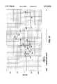
- FIGS. 12 and 13are a graph of change in voltage, dV, versus time measured in a test of the circuit of FIG. 9;
- FIG. 14is an electrical diagram of a memory unit according to the invention and another circuit used to test it;
- FIG. 15is a time versus voltage curve showing the retention of a measurable polarization state by the memory unit tested in FIG. 12 for nearly 100 hours;
- FIGS. 16 through 21show electrical circuit diagrams of six different alternative embodiments of a memory unit according to the invention.
- FIG. 22is a perspective view of an exemplary memory unit according to the invention on which various dimensions are labeled.
- FIG. 23is an equivalent circuit of the memory unit of FIG. 22.
- Memory 100includes a memory cell 10 which comprises a memory unit 12 in which information is stored, plus transistor switches 14, 15, 16, 18, and 19, signal inputs 21, 22, and 23 to operate the memory unit 12, a load capacitor 25, and a load resistor 26. Electronic grounds are indicated by triangles, such as 28.
- Memory unit 12includes a ferroelectric capacitor 30, and a transistor 32. In the embodiment shown in FIG. 1, the ferroelectric capacitor 30 is connected to the gate 33 of transistor 32.
- the memory unit 12is able to store information because the polarization state of capacitor 30 determines the voltage on the gate 33 of transistor 32, thereby changing the current across the transistor 32 and voltage developed across load resistor 26, and thus the voltage output to bit line 43.
- the cell 10is addressed via word line 42 and bit line 43.
- Word line 42carries a signal W which is high when the cell is written-to and read and low otherwise.
- Bit line 43carries a high voltage when a logic "1" is to be written to capacitor 30 and a zero or low voltage when a logic "0" is to be written to capacitor 30.
- a high data output signali.e. a voltage higher than a second reference voltage, Vref2, which in the embodiments discussed below is about 0.850 volts, is output to bit line 43 if capacitor 30 is in a logic "1" state and when cell 10 is read, and a low data output signal, i.e.
- a voltage lower than the second reference voltageis output to bit line 43 if capacitor 30 is in a logic "0" state when cell 10 is read.
- cell address circuitry 45decodes a signal received on address cable 46 to control transistors 14, 15, 16, and 19 appropriately and provide signals ⁇ 1, ⁇ 1*, and ⁇ 2 so as to properly read and write to the cell 10.
- data in/out circuitry 41decodes data received on data line 44 and provides appropriate signals on bit line 44 to be written to the cell 10, and also differentiates between the data output signal voltages output to bit line 43 to provide a data output signal on data cable 44.
- a sense amplifier 53 in data in/out circuitry 41utilizes the second reference voltage, Vref2, input at 54 to differentiate between the data signals output on bit line 43.
- a complete memory 100is composed of an array of memory cells 10 arranged in rows and columns as indicated by the dotted lines in FIG. 1.
- the word line 42addresses each of the cells in the same row as the cell 10, while the bit line 43 addresses each of the cells in the same column as cell 10.
- an individual cellis addressed when the word line and the bit line in the array corresponding to the cell are simultaneously activated.
- the word line 42goes high turning on transistors 14 and 15 thereby connecting first electrode 47 of capacitor 30 to the 1/2Vdd reference voltage and second electrode 49 of capacitor 30 to bit line 43. If bit line 43 is carrying a high signal, capacitor 30 is polarized in one direction, and if bit line 43 is carrying a low signal, capacitor 30 is polarized in the opposite direction.
- the signals W, ⁇ 1, ⁇ 1*, and ⁇ 2are used to place a signal on bit line 43 that is higher than the second reference voltage, Vref2, if the polarization on capacitor 30 is in the logic "1" state and to place a signal on bit line 43 that is lower than the second reference voltage, Vref2, if the polarization of capacitor 30 is in the logic "0" state.
- the signal ⁇ 1*is the inverse of the signal ⁇ 1.
- the portion of the memory cell 10 that actually stores informationis memory unit 12.
- the memory unit 12is shown separately in FIG. 2.
- a feature of the inventionis that the memory unit 12 is a four-terminal memory unit. Terminals 61 and 62 are used to write information into the unit, while terminals 63 and 64 are used to read the information from the unit.
- FIG. 3shows an embodiment of the memory unit of the invention in which the transistor 80 is a bipolar transistor having an emitter 81, a collector 82, and a base 83. Otherwise the embodiment is the same as that of FIG. 2.
- the various components that are the samebear the same numerals for clarity. Other types of transistors may also be used.
- FIGS. 4-8Illustrations of how the circuit of FIG. 2, as it may be embodied in an integrated circuit, are shown in FIGS. 4-8.
- the active regionsare generally referred to as sources and drains since the embodiments show MOSFET transistors.
- the inventioncan also be embodied in other types of transistors, such as bipolar transistors in which the active areas are referred to as emitters and collectors.
- the term "active regions"is used to broadly include all of the terminology conventionally used to refer to such regions in any type of transistor.
- a substrate 69preferably formed of a single crystal of doped silicon, has active regions 65 and 66 formed in it by doping. As is known in the art, the doping of substrate 69 is opposite to the doping of active regions 65 and 66: one is p-type and the other is n-type. Active regions 65 and 66 are the source and drain of a MOS transistor 32 in this embodiment. The active regions 65 and 66 may also be formed in trenches in the substrate 69 or on the substrate 69 as is known in the art.
- a gate insulating layer 68is formed on the substrate 69, and a gate layer 67 is formed on the insulating layer 68.
- Gate layer 67is preferably formed of a metal such as platinum but also may be formed of other conductors, such as other metals or doped polysilicon.
- a layer 50 of a ferroelectric materialis formed on the gate layer 67, and a conductive layer 60 is formed on the ferroelectric layer 50.
- Ferroelectric layer 50is preferably made of a layered superlattice material as described in U.S. patent application Ser. No. 965,190, but also may be formed of other ferroelectrics. In the examples discussed below, the ferroelectric material 50 was strontium bismuth tantalate.
- Conductive layer 60is preferably made of platinum, but also may be made of other suitable conductive materials.
- conductive layers 67 and 60are generally formed of multiple layers of conductive materials which may include an adhesive layer, such as titanium, and a barrier layer, such as titanium nitride. However, these multiple layers are not shown herein since they are not directly related to the invention and may cause confusion.
- the lower electrode 47 of the capacitor 30is formed of the same conductive layer 67 as the gate 33 of transistor 32. However the ferroelectric material 50 is spaced some distance from the transistor to isolate the two.
- the four terminals 61-64are shown schematically, and generally will be implemented as "metallization" layers made of polysilicon, platinum, aluminum or other materials conventionally used for metallization layers in integrated circuits.
- Each of the layers 60, 47, 67, and 68is a thin film of from about 500 ⁇ to 4000 ⁇ in thickness. The relative thicknesses of these layers, the active regions 65 and 66, and the substrate 69 are known in the art.
- FIG. 5Another embodiment of the memory unit 500 according to the invention is shown in FIG. 5. This embodiment is the same as that of FIG. 4, except the ferroelectric layer 50 and the second electrode 49 are formed in a stack above the transistor 32.
- FIGS. 6 and 7Further embodiments of a memory unit 600, 700 according to the invention is shown in FIGS. 6 and 7. These embodiments are closer to the ferroelectric FETs in the prior art and approach the problem of saturating the polarization of the ferroelectric capacitor 30A in a slightly different manner than the embodiments discussed above.
- source regions 71, 81 and drain regions 77, 82 respectivelyare extended under the gate 33A, 33B enabling these heavily doped regions to be utilized as bottom electrodes for a metal-ferroelectric-substrate or metal-ferroelectric-insulator-substrate capacitor.
- These configurationsalso eliminate the need for a fourth terminal, i.e. the terminal 62 in FIGS. 1-4.
- first active region 71 and doped second active region 72are formed.
- these active regions 71 and 72are heavily doped as to be highly conductive.
- a channel region 73is formed between the active regions 71 and 77.
- a ferroelectric layer 74is formed overlying channel region 73, a portion 71A of first active region 71, and a portion 72A of second active region 72.
- Conductive layer 75is formed on ferroelectric layer 74 and also overlies channel region 73, portion 71A of first active region 71, and portion 72A of second active region 72. Terminals 76, 78, and 79 connect the conductive layers to external signals as described in reference to FIG. 1.
- Terminals 78 and 79also serve the same function as terminal 62 in the embodiments of FIGS. 1-4, as well as the function of terminals 63 and 64.
- the first electrode 47A of capacitor 30Ais formed from portion 71A of first active region 71 and portion 72A of second active region 72
- gate 33A of transistor 32Ais formed of the same conductive member 75 as the second electrode 49A of the ferroelectric capacitor 30A.
- An important aspect of this embodimentis that the length of channel 73 is much smaller than the width of gate 33A, particularly as compared to prior art ferroelectric FET's in which the length of channel 73 is equal to, or nearly equal to, the gate width.
- the distance in the direction parallel to the ferroelectric layer 74 and the gate/second electrode layer 75 spanned by the channel 73is short relative to the distance spanned by the first electrode 47A in the same direction, i.e. the horizontal direction in FIG. 6.
- the distance spanned by the first electrode 47Ais equal to or greater than the distance spanned by the channel 73.
- the channel 73typically spans the entire, or nearly the entire, distance underlying the ferroelectric 74 and gate member 75.
- the active areas 71 and 72are highly doped making them very conductive.
- the memory unit 600includes a distinct capacitive function. That is, unit 600 is not just a FET, but is a combination FET 32A and capacitor 30A. Except for the spans of the first electrode 47A and the channel region 73, the dimensions and the materials of the memory unit 600 are within the ranges described above and generally known in the art.
- the memory unit 700 according to the invention shown in FIG. 7is the same as the embodiment of FIG. 6, except that it also includes an insulating layer 86 Since the extensions 81A and 82A provide a definite capacitive function, a lower dielectric constant insulator, such as silicon dioxide, will work better in this embodiment than the prior art, and in some cases is necessary to prevent material compatibility problems. However, preferably a material having a relatively high dielectric constant, such as barium Strontium titanate is used. Preferably the dielectric constant of insulating layer 86 is greater than 50. As in the embodiment of FIG. 6, memory unit 700 only includes three terminals 87, 88, and 89.
- Terminals 88 and 89may serve as both the read terminals and the write terminal for the first electrode 47B.
- the embodiment of FIG. 7includes a ferroelectric layer 84, a conductive layer 85, and active regions 81 and 82.
- the first electrode of capacitor 30Bcomprises portion 81A of first active region 81 and portion 82A of second active region 82.
- Layer 85acts as both gate 33B and the second electrode 49B of capacitor 30B. Again the length of channel 83 is much smaller than the width of gate 33B.
- the terminal 61, 76, 87 connected to the second electrodewill at some point be connected to one of the active regions or substrate of the corresponding transistor, or to a reference potential common to such active region or substrate of the corresponding transistor, so that the polarization alters the manner in which the transistor conducts and/or the threshold voltage of the transistor. It has been found that polarizing the capacitor 30, 30A, 30B alters the threshold voltage at which the transistor 32, 32A, 32B conducts such that the conduction of current from the source to the drain is a function of the polarization direction.
- the transistor threshold voltagecan be changed from its value without a ferroelectric polarization present, to new threshold voltage values that depend on the direction of polarization of the ferroelectric capacitor 30, 30A, 30B. This is similar to what others have tried to accomplish in the references discussed in the Background of the Invention section above. However, as will be shown below, testing has shown that, unlike the prior art devices, the devices according to the invention retain their programmed threshold voltage values for at least several weeks.
- FIG. 9shows an electrical circuit which was used to test the invention.
- the circuitincludes a pulsed voltage source or pulser 91, ferroelectric capacitor 92, load capacitor 93, transistor 94, and load resistor 95.
- One electrode 92B of ferroelectric capacitor 92is connected to pulser 91 via switch S3 and the other electrode 92A is connected to ground through switch S1 and load capacitor 93 and to the gate 94A of transistor 94.
- the drain 94B of transistor 94is connected to a voltage source Vdd, and the source 94C of the transistor 94 is connected to ground through a load resistor 95.
- the top electrode 92Bis connected to ground when switch S3 is in the ground position G and connected to the pulser 91 when switch S3 is in the closed position C.
- the bottom electrode 92Ais connected to ground when switch S1 is in the closed position C and is connected to the gate 94A of transistor 94 when switch S2 is in the closed position C.
- the gate 94Ais connected to ground.
- the substrate on which the ferroelectric capacitor was fabricatedwas connected to ground through a 24 picofarad capacitor to keep the test circuit from floating.
- the ferroelectric capacitor 92was 500 ⁇ 500 micrometer squared in area and had an approximate thickness of 1700 ⁇ .
- the ferroelectric materialwas strontium bismuth tantalate.
- Load capacitor 93was 140 nanofarads, transistor 94 was an n-channel, depletion mode type, and resistor 95 was 1 kilohm.
- the drain voltage Vddwas adjusted to obtain an output reference voltage, Vout, of 0.850 volts when the switch S2 was connected to ground, that is, when the gate 94A was held at ground.
- Hysteresis curveswere obtained for the above circuit by replacing the pulser 91 with a signal generator and performing a compensated Sawyer-Tower hysteresis measurement using a triangular signal of 1 kilohertz frequency. Switches S1, S2, and S3 were closed. The x-axis voltage was tapped off the top electrode 92B of ferroelectric capacitor 92. The hysteresis curve of FIG. 10 was obtained when the y-axis voltage was tapped off the gate side of switch S2, and the hysteresis curve of FIG. 11 was obtained when the y-axis voltage was Vout. The voltage in each of the curves is in millivolts (mV). Both curves are relatively boxy and vertical, indicating a fully saturated response that should produce good memory performance.
- FIGS. 12 and 13A time retention test was run on the test circuit of FIG. 9 with the results shown in FIGS. 12 and 13.
- the voltage differential, dV, measured at Voutis shown, dV being the difference between the reference voltage of 0.850 volts and the measured voltage.
- the x-axisshows the time in military time, beginning at 1100 hours on the first day.
- the time scaleis "broken" at two points on FIG. 12 and between FIG. 12 and FIG. 13 to fit the chart on two pages.
- the initial time scaleis 1 inch per minute, but at 11:30 a.m. on the first day the scale is changed to 8 inches per hour.
- the ferroelectric capacitorwas "reset” by closing switch S1, switching switch S3 to ground, and closing switch S2.
- the node 902was then manually taken to ground for a brief time to ensure that the electrodes 92A and 92B were at the same ground potential. This put both sides of capacitors 92 and 93 and the gate 94A of transistor 94 at ground.
- a +1.5 volt pulse of 1 microsecond durationwas applied to the circuit by pulser 91.
- a positive dV of about 130 millivoltswas recorded across resistor 95 at Vout. The signal across the resistor 95 began to decay.
- switch S1was opened to remove the load capacitor from the circuit, and switch S3 was switched to ground to ground the top electrode 92B of the ferroelectric capacitor 92.
- switch S1was closed to put the load capacitor back in the circuit.
- FIG. 14a circuit with two pulse generators was built as shown in FIG. 14. This circuit is the same as that of FIG. 9, except that only two switches, S1 and S2 are used and the voltage source Vdd was replaced by a second pulse generator 97.
- a 500 ⁇ 500 micrometer squared capacitor utilizing strontium bismuth tantalate as the ferroelectric materialwas again used along with an n-type depletion mode transistor 94 having drain 94B and source 94C, a 140 nanofarad load capacitor 93, and a 1 kilohm load resistor 95. Again the system was initialized by turning switch S2 to ground and setting Vout to be 850 millivolts.
- dVwas periodically measured over a 93 hour period for the case of polarization with a positive pulse, and over a 95 hour period for the case of polarization with a negative pulse.
- the voltagedecayed exponentially at first, then settled down to a slowly decaying value of about 10 millivolts in the case of the positive polarization and about 15 millivolts in the case of the negative polarization.
- test circuitsas well as the circuit of FIG. 1 may be made in a variety of different configurations than those shown.
- the voltage to which first electrode 92A is connected when the capacitor 92 is being polarized and the voltage to which the gate 94A is connected when the system is being initializeddo not have to be a ground. They may be any constant voltage source that can provide a "zero" reference for the capacitor and gate.
- the memory unit 12can take on many different configurations than the configuration shown in FIGS. 2 and 3. Some of the possible configurations are shown in FIG. 16 through 21. It is understood that each of these memory units 160, 170, 180, 190, 210, and 220 are to be incorporated into a memory circuit, such as that shown in FIG. 1, to make an operable memory.
- FIG. 16shows an memory unit 160 that includes a ferroelectric capacitor 161, a first MOS transistor 163, and a second MOS transistor 164.
- the ferroelectric capacitor 161is connected to the gate 162 of the first MOS transistor, and the drain 166 of the first transistor is connected to the drain 167 of the second transistor.
- FIG. 17shows a memory unit 170 comprising first ferroelectric capacitor 171, second ferroelectric capacitor 172, first MOS transistor 175, and second MOS transistor 176.
- the first ferroelectric capacitor 171is connected to the gate of the first transistor 175, while the second ferroelectric capacitor 172 is connected to the gate of the second transistor 176.
- the drains of the transistors 175 and 176are connected together.
- FIG. 18shows a memory unit 180 comprising first ferroelectric capacitor 181, second ferroelectric capacitor 182, first MOS transistor 183, and second MOS transistor 184.
- the first ferroelectric capacitor 181is connected to the gate of the first transistor 183, while the second ferroelectric capacitor 182 is connected to the gate of the second transistor 184.
- the drains of the transistors 183 and 184are connected together as are the sources.
- FIG. 19shows a memory unit 190 comprising ferroelectric capacitor 191, p-channel MOS transistor 192, and n-channel MOS transistor 193.
- the two transistors 192 and 193comprise a CMOS pair.
- the ferroelectric capacitor 191is connected to the gates of both transistors 192 and 193 and the drains of the transistors 192 and 193 are connected together.
- FIG. 20shows a memory unit 200 comprising a CMOS pair of transistors 204 and 205 and N ferroelectric capacitors 201A, 201B . . . 201N. Each capacitor is connected to the gates of the transistors 204 and 205.
- FIG. 21shows a memory unit 210 including N ferroelectric capacitors, 211A, 211 B, . . . . 211N and a single MOS transistor 214. Each of the N capacitors 211A, 211B, . . . 211N are connected to the gate of the transistor 214.
- These two embodimentslend themselves to a neural network in which each of the capacitors, such as 221A, 221 B, . . . 221N provides a synaptic weight, which weights are integrated by the transistor pair 224, 225 or transistor 214.
- each of the ferroelectric capacitorsare connected into the circuit and fabricated in an integrated circuit such that their polarization states can be saturated.
- each of the ferroelectric capacitorsare connected into a circuit such that the electrode not connected to the gate of the transistor, i.e. the second electrode, is connected to an active region or substrate of the transistor so that the capacitor polarization alters the manner in which the transistor conducts and/or the threshold voltage of the transistor.
- thiscan be accomplished in many ways, such as by connecting both the capacitor second electrode and the appropriate active region or substrate to ground, to the same reference voltage, etc.
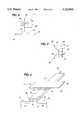
- FIG. 22shows a perspective view of a memory unit 220 according to the invention which will be useful in a discussion below of the preferred parameters of the memory unit structure.
- the memory unit 220is fabricated on a silicon substrate 222, and includes field oxide regions 224, transistor 232 and ferroelectric capacitor 230.
- the transistor 232includes a source 265 and drain 266 formed by doped regions in silicon substrate 222, gate oxide layer 268, and gate 233 formed of conductive layer 267.
- Ferroelectric capacitorincludes first electrode 247, also formed of conductive layer 267, ferroelectric layer 250, and second electrode 249 formed of conducting layer 260.
- FIG. 23shows an equivalent circuit 221 of the memory unit 220.
- Equivalent circuit 221includes ferroelectric capacitor 230, load capacitor 240 and transistor 232.
- the load capacitance of the unit 220is dominated by the gate capacitance of the transistor, that is the capacitance between the gate 233 and the channel region 235 of the transistor 232.
- the circuit 221can also be considered to be an equivalent circuit to the test circuit of FIG. 14 with switches S1 and S2 closed, since, in FIG. 14, one side of load resistor 93 and the source 94C of transistor 94 are connected to ground.
- the preferred embodiments of the inventioninclude certain preferred relationships between the relative magnitude of the capacitance, CF, of the ferroelectric capacitor 230 and the capacitance, CL, of the load capacitor 240.
- AgWb, where W is the channel width and is indicated in FIG. 23, and b is the amount the gate 233 overlaps the source 265 and drain 266.
- AfWL, where L is the length of the ferroelectric capacitor 230.
- ais approximately the depth source 265 and drain 266 penetrate into substrate 222.
- bis preferably made larger, for example as shown in FIGS. 6 and 7.
- Rcis approximately the depth source 265 and drain 266 penetrate into substrate 222.
- the gate oxide 268being the conventional silicon dioxide, having a dielectric constant of about 4
- an insulator with a higher dielectric constantsay tantalum oxide, Ta 2 O 5 , which has a dielectric constant of about 25
- the value of Rccan be reduced to 0.4, which should easily permit a practical, workable memory device.
- the capacitance Cf of the ferroelectric capacitor 230should be less than five times the load capacitance, i.e. Cf ⁇ 5 ⁇ Cl, or in other words, the ratio of the ferroelectric and load capacitances, Rc, should be less than or equal to 5, i.e., Rc ⁇ 5.
- the dielectric constant of the gate insulator 268,is preferably greater than the dielectric constant of silicon dioxide, i.e. greater than 4, that is, ⁇ g>4.
- the dielectric constant, ⁇ g, of the gate insulatoris preferably greater than or equal to the dielectric constant, ⁇ f, divided by 8, i.e. ⁇ g ⁇ f/8. This value, coupled with the other preferred parameters will generally provide a practical memory unit 220.
- the ferroelectric capacitormay be fabricated on the field oxide 224 of the cell rather than directly overlaying the transistor 232 as discussed above, if the preferred parameters are used.
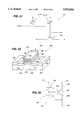
- FIG. 8Such a structure is shown in FIG. 8.
- the memory unit 800comprises transistor 893 and capacitor 894 which are fabricated according to the above parameters.
- the capacitor 894is fabricated on field oxide 891 which is conventionally grown on substrate 801.
- Transistor gate 895 and capacitor electrode 896are connected via a wiring layer 897.
- Other details of the structure, such as the other connections to the transistor 893 and capacitor 894are not shown for clarity.
- FIGS. 4-7 and 22are highly desirable, they are not necessary, if the unit cell structure utilizes the preferred relative dimensions and other parameters. Fabrication of the capacitor on the field oxide permits better isolation of the ferroelectric material from the transistor. Thus, use of the parameters of the invention enables ferroelectric materials that are less compatible with conventional integrated circuit technology to be used more successfully. However, when the ferroelectric material is compatible with conventional integrated circuit transistor technology, the combination of the architectures of FIGS. 4-7 and 22 in combination with the parameters of the invention is preferred.
- non-volatile memorythat includes a ferroelectric memory unit that includes a combination of a ferroelectric capacitor and transistor and that provides saturated polarization and has many other advantages.
- a ferroelectric memory unitthat includes a combination of a ferroelectric capacitor and transistor and that provides saturated polarization and has many other advantages.
- the particular embodiments shown in the drawings and described within this specificationare for purposes of example and should not be construed to limit the invention which will be described in the claims below.
- those skilled in the artmay now make numerous uses and modifications of the specific embodiments described, without departing from the inventive concepts.
- the memory units according to the inventionmay be used with other memory cell and memory architectures. Equivalent structures, materials and process may be substituted for the various structures, materials and processes described.
Landscapes
- Engineering & Computer Science (AREA)
- Computer Hardware Design (AREA)
- Non-Volatile Memory (AREA)
- Dram (AREA)
- Semiconductor Memories (AREA)
Abstract
Description
Vf=Va/(1+Rc). (1)
Rc=Cf/Cg=εfAfc/εgAgt. (2)
Claims (21)
Priority Applications (6)
| Application Number | Priority Date | Filing Date | Title |
|---|---|---|---|
| US08/224,241US5523964A (en) | 1994-04-07 | 1994-04-07 | Ferroelectric non-volatile memory unit |
| US08/405,885US6133050A (en) | 1992-10-23 | 1995-03-17 | UV radiation process for making electronic devices having low-leakage-current and low-polarization fatigue |
| PCT/US1995/003758WO1995027982A1 (en) | 1994-04-07 | 1995-03-30 | Non-volatile memory |
| JP7526357AJPH08511895A (en) | 1994-04-07 | 1995-03-30 | Non-volatile storage device |
| US08/482,765US5559733A (en) | 1994-04-07 | 1995-06-07 | Memory with ferroelectric capacitor connectable to transistor gate |
| US09/686,552US6559469B1 (en) | 1992-10-23 | 2000-10-11 | Ferroelectric and high dielectric constant transistors |
Applications Claiming Priority (1)
| Application Number | Priority Date | Filing Date | Title |
|---|---|---|---|
| US08/224,241US5523964A (en) | 1994-04-07 | 1994-04-07 | Ferroelectric non-volatile memory unit |
Related Parent Applications (1)
| Application Number | Title | Priority Date | Filing Date |
|---|---|---|---|
| US96519092AContinuation-In-Part | 1988-12-27 | 1992-10-23 |
Related Child Applications (2)
| Application Number | Title | Priority Date | Filing Date |
|---|---|---|---|
| US08/405,885Continuation-In-PartUS6133050A (en) | 1992-10-23 | 1995-03-17 | UV radiation process for making electronic devices having low-leakage-current and low-polarization fatigue |
| US08/482,765DivisionUS5559733A (en) | 1994-04-07 | 1995-06-07 | Memory with ferroelectric capacitor connectable to transistor gate |
Publications (1)
| Publication Number | Publication Date |
|---|---|
| US5523964Atrue US5523964A (en) | 1996-06-04 |
Family
ID=22839839
Family Applications (2)
| Application Number | Title | Priority Date | Filing Date |
|---|---|---|---|
| US08/224,241Expired - LifetimeUS5523964A (en) | 1992-10-23 | 1994-04-07 | Ferroelectric non-volatile memory unit |
| US08/482,765Expired - Fee RelatedUS5559733A (en) | 1994-04-07 | 1995-06-07 | Memory with ferroelectric capacitor connectable to transistor gate |
Family Applications After (1)
| Application Number | Title | Priority Date | Filing Date |
|---|---|---|---|
| US08/482,765Expired - Fee RelatedUS5559733A (en) | 1994-04-07 | 1995-06-07 | Memory with ferroelectric capacitor connectable to transistor gate |
Country Status (3)
| Country | Link |
|---|---|
| US (2) | US5523964A (en) |
| JP (1) | JPH08511895A (en) |
| WO (1) | WO1995027982A1 (en) |
Cited By (65)
| Publication number | Priority date | Publication date | Assignee | Title |
|---|---|---|---|---|
| US5592411A (en)* | 1995-11-02 | 1997-01-07 | Motorola, Inc. | Non-volatile register and method for accessing data therein |
| US5596214A (en)* | 1994-05-30 | 1997-01-21 | Nec Corporation | Non-volatile semiconductor memory device having a metal-insulator-semiconductor gate structure and method for fabricating the same |
| US5663588A (en)* | 1994-07-12 | 1997-09-02 | Nippondenso Co., Ltd. | Semiconductor device having an SOI structure of mesa isolation type and manufacturing method therefor |
| US5721700A (en)* | 1996-01-26 | 1998-02-24 | Nec Corporation | Non-volatile semiconductor memory device in which applied voltage to ferroelectric capacitor is adjusted |
| US5877977A (en)* | 1996-09-10 | 1999-03-02 | National Semiconductor Corporation | Nonvolatile memory based on metal-ferroelectric-metal-insulator semiconductor structure |
| US5932903A (en)* | 1995-08-23 | 1999-08-03 | Sharp Kabushiki Kaisha | Ferroelectric semiconductor memory cell, a memory and a method for accessing the same |
| US5959879A (en)* | 1997-06-09 | 1999-09-28 | Samsung Electronics Co., Ltd. | Ferroelectric memory devices having well region word lines and methods of operating same |
| US5978253A (en)* | 1997-05-09 | 1999-11-02 | Samsung Electronics Co., Ltd. | Methods of operating integrated circuit memory devices having nonvolatile single transistor unit cells therein |
| EP0811982A3 (en)* | 1996-06-06 | 1999-11-17 | Nec Corporation | Non-volatile ferroelectric memory device for storing data bits restored upon power-on and intermittently refreshed |
| US5999439A (en)* | 1995-09-11 | 1999-12-07 | Micron Technology, Inc. | Ferroelectric memory using ferroelectric reference cells |
| US6031754A (en)* | 1998-11-02 | 2000-02-29 | Celis Semiconductor Corporation | Ferroelectric memory with increased switching voltage |
| US6049477A (en)* | 1997-12-09 | 2000-04-11 | Fujitsu Limited | Ferroelectric memory device in which the channel region has the same conductivity type as the diffusion region |
| EP0982779A3 (en)* | 1998-08-28 | 2000-05-17 | Semiconductor Technology Academic Research Center | Memory structure in ferroelectric nonvolatile memory and readout method therefor |
| US6069381A (en)* | 1997-09-15 | 2000-05-30 | International Business Machines Corporation | Ferroelectric memory transistor with resistively coupled floating gate |
| WO2000070685A1 (en)* | 1999-05-19 | 2000-11-23 | Symetrix Corporation | Ferroelectric memory with disturb protection |
| US6171934B1 (en) | 1998-08-31 | 2001-01-09 | Symetrix Corporation | Recovery of electronic properties in process-damaged ferroelectrics by voltage-cycling |
| EP1054406A3 (en)* | 1999-05-19 | 2001-01-17 | Semiconductor Technology Academic Research Center | Ferroelectric non-volatile memory device |
| US6198652B1 (en)* | 1998-04-13 | 2001-03-06 | Kabushiki Kaisha Toshiba | Non-volatile semiconductor integrated memory device |
| WO2001024237A1 (en)* | 1999-09-28 | 2001-04-05 | Symetrix Corporation | Integrated circuits with barrier layers and methods of fabricating same |
| US6225655B1 (en)* | 1996-10-25 | 2001-05-01 | Texas Instruments Incorporated | Ferroelectric transistors using thin film semiconductor gate electrodes |
| US6236076B1 (en) | 1999-04-29 | 2001-05-22 | Symetrix Corporation | Ferroelectric field effect transistors for nonvolatile memory applications having functional gradient material |
| US6255121B1 (en) | 1999-02-26 | 2001-07-03 | Symetrix Corporation | Method for fabricating ferroelectric field effect transistor having an interface insulator layer formed by a liquid precursor |
| US6326651B1 (en)* | 1999-03-08 | 2001-12-04 | Matsushita Electric Industrial Co., Ltd. | Field-programmable gate array with ferroelectric thin film |
| US6326315B1 (en) | 2000-03-09 | 2001-12-04 | Symetrix Corporation | Low temperature rapid ramping anneal method for fabricating layered superlattice materials and making electronic devices including same |
| US6335550B1 (en)* | 1999-02-26 | 2002-01-01 | Sharp Kabushiki Kaisha | Fet with ferroelectric gate |
| US6339238B1 (en) | 1998-10-13 | 2002-01-15 | Symetrix Corporation | Ferroelectric field effect transistor, memory utilizing same, and method of operating same |
| WO2001069602A3 (en)* | 2000-03-10 | 2002-02-21 | Symetrix Corp | Ferroelectric memory and method of operating same |
| US6365927B1 (en) | 2000-04-03 | 2002-04-02 | Symetrix Corporation | Ferroelectric integrated circuit having hydrogen barrier layer |
| US6373743B1 (en) | 1999-08-30 | 2002-04-16 | Symetrix Corporation | Ferroelectric memory and method of operating same |
| US6372518B1 (en) | 2000-01-26 | 2002-04-16 | Matsushita Electric Industrial Co., Ltd. | Method using unreactive gas anneal and low temperature pretreatment for fabricating layered superlattice materials and making electronic devices including same |
| US6441414B1 (en) | 1998-10-13 | 2002-08-27 | Symetrix Corporation | Ferroelectric field effect transistor, memory utilizing same, and method of operating same |
| US6512256B1 (en) | 1998-11-20 | 2003-01-28 | Symetrix Corporation | Integrated circuit having self-aligned hydrogen barrier layer and method for fabricating same |
| US6559469B1 (en) | 1992-10-23 | 2003-05-06 | Symetrix Corporation | Ferroelectric and high dielectric constant transistors |
| US6562678B1 (en) | 2000-03-07 | 2003-05-13 | Symetrix Corporation | Chemical vapor deposition process for fabricating layered superlattice materials |
| US6580633B2 (en)* | 2000-09-28 | 2003-06-17 | Seiko Epson Corporation | Nonvolatile semiconductor memory device |
| US6582972B1 (en) | 2000-04-07 | 2003-06-24 | Symetrix Corporation | Low temperature oxidizing method of making a layered superlattice material |
| US20030141527A1 (en)* | 2002-01-30 | 2003-07-31 | Joo Heung-Jin | Ferroelectric integrated circuit devices having an oxygen penetration path and methods for manufacturing the same |
| US6603180B1 (en)* | 1997-11-28 | 2003-08-05 | Advanced Micro Devices, Inc. | Semiconductor device having large-area silicide layer and process of fabrication thereof |
| US20030183859A1 (en)* | 2000-08-24 | 2003-10-02 | Gnadinger Fred P. | Single transistor rare earth manganite ferroelectric nonvolatile memory cell |
| DE10212926A1 (en)* | 2002-03-22 | 2003-10-16 | Infineon Technologies Ag | Semiconductor storage cell has a modulation region arranged between a first gate electrode of a gate electrode arrangement and an insulating region |
| US6649963B1 (en)* | 1997-03-07 | 2003-11-18 | Sharp Laboratories Of America, Inc. | Ferroelectric memory cell for VLSI RAM |
| US20030218899A1 (en)* | 2002-05-21 | 2003-11-27 | Byung-Gil Jeon | Ferroelectric memory devices having a plate line control circuit and methods for operating the same |
| US6674110B2 (en) | 2001-03-02 | 2004-01-06 | Cova Technologies, Inc. | Single transistor ferroelectric memory cell, device and method for the formation of the same incorporating a high temperature ferroelectric gate dielectric |
| US20040032762A1 (en)* | 2002-08-13 | 2004-02-19 | General Semiconductor Inc. | DMOS device with a programmable threshold voltage |
| US20040041186A1 (en)* | 2002-08-28 | 2004-03-04 | Klaus Dimmler | Ferroelectric transistor with enhanced data retention |
| US6714435B1 (en) | 2002-09-19 | 2004-03-30 | Cova Technologies, Inc. | Ferroelectric transistor for storing two data bits |
| US20040109367A1 (en)* | 2002-07-23 | 2004-06-10 | Matsushita Electric Incustrial Co., Ltd. | Ferroelectric element and a ferroelectric gate device using the same |
| US20040135182A1 (en)* | 2002-11-11 | 2004-07-15 | Hyeong-Geun An | Ferroelectric capacitors including a seed conductive film and methods for manufacturing the same |
| US20040169202A1 (en)* | 2003-02-28 | 2004-09-02 | Hyun-Yul Kang | Ferroelectric memory devices having an expanded plate electrode and methods for fabricating the same |
| US6888736B2 (en) | 2002-09-19 | 2005-05-03 | Cova Technologies, Inc. | Ferroelectric transistor for storing two data bits |
| US20050094457A1 (en)* | 1999-06-10 | 2005-05-05 | Symetrix Corporation | Ferroelectric memory and method of operating same |
| US20050212022A1 (en)* | 2004-03-24 | 2005-09-29 | Greer Edward C | Memory cell having an electric field programmable storage element, and method of operating same |
| US20060071255A1 (en)* | 2004-09-24 | 2006-04-06 | Bomy Chen | Non-destructive read ferroelectric memory cell, array and integrated circuit device |
| US20070009821A1 (en)* | 2005-07-08 | 2007-01-11 | Charlotte Cutler | Devices containing multi-bit data |
| US20070190670A1 (en)* | 2006-02-10 | 2007-08-16 | Forest Carl A | Method of making ferroelectric and dielectric layered superlattice materials and memories utilizing same |
| US7295583B2 (en) | 1995-06-02 | 2007-11-13 | Matsushita Electric Industrial Co., Ltd. | Optical device, laser beam source, laser apparatus and method of producing optical device |
| US20090161460A1 (en)* | 2007-12-21 | 2009-06-25 | Qimonda Ag | Retention test system and method for resistively switching memory devices |
| US20140085963A1 (en)* | 2012-09-25 | 2014-03-27 | Palo Alto Research Center Incorporated | Systems and methods for writing and non-destructively reading ferroelectric memories |
| CN104934425A (en)* | 2014-03-21 | 2015-09-23 | 意法半导体(鲁塞)公司 | Memory device hardened against accidental flipping associated with SRAM memory plane and non-volatile memory plane |
| US20160379703A1 (en)* | 2015-06-23 | 2016-12-29 | Palo Alto Research Center Incorporated | Circuit for reading ferroelectric memory |
| US9679893B2 (en)* | 2015-05-15 | 2017-06-13 | Taiwan Semiconductor Manufacturing Company Limited | Semiconductor device and transistor |
| US11502103B2 (en)* | 2018-08-28 | 2022-11-15 | Intel Corporation | Memory cell with a ferroelectric capacitor integrated with a transtor gate |
| US20240013829A1 (en)* | 2020-11-20 | 2024-01-11 | Semiconductor Energy Laboratory Co., Ltd. | Semiconductor device |
| US11943933B2 (en) | 2020-06-29 | 2024-03-26 | Taiwan Semiconductor Manufacturing Company Limited | Ferroelectric memory device using back-end-of-line (BEOL) thin film access transistors and methods for forming the same |
| US11980037B2 (en) | 2020-06-19 | 2024-05-07 | Intel Corporation | Memory cells with ferroelectric capacitors separate from transistor gate stacks |
Families Citing this family (34)
| Publication number | Priority date | Publication date | Assignee | Title |
|---|---|---|---|---|
| JP3505758B2 (en)* | 1993-12-28 | 2004-03-15 | ローム株式会社 | Non-volatile semiconductor memory |
| US5753946A (en)* | 1995-02-22 | 1998-05-19 | Sony Corporation | Ferroelectric memory |
| JP3279453B2 (en)* | 1995-03-20 | 2002-04-30 | シャープ株式会社 | Non-volatile random access memory |
| US5930171A (en)* | 1995-05-22 | 1999-07-27 | Siemens Aktiengesellschaft | Constant-current source with an EEPROM cell |
| KR100355379B1 (en)* | 1995-06-07 | 2002-12-16 | 삼성전자 주식회사 | Ferroelectric memory device and driving method thereof |
| US5629229A (en)* | 1995-07-12 | 1997-05-13 | Sharp Kabushiki Kaisha | Metalorganic chemical vapor deposition of (Ba1-x Srx)RuO3 /(Ba1-x Srx)TIO3 /(Ba1-x Srx)TiO3 /(Ba1- Srx)RuO3 capacitors for high dielectric materials |
| JP2800745B2 (en)* | 1995-11-10 | 1998-09-21 | 日本電気株式会社 | Ferroelectric memory |
| KR100189982B1 (en)* | 1995-11-29 | 1999-06-01 | 윤종용 | Manufacturing method of high dielectric capacitor |
| US5966318A (en)* | 1996-12-17 | 1999-10-12 | Raytheon Company | Nondestructive readout memory utilizing ferroelectric capacitors isolated from bitlines by buffer amplifiers |
| TW360977B (en)* | 1998-03-13 | 1999-06-11 | Winbond Electronics Corp | DRAM and circuit structure thereof |
| US6046929A (en)* | 1998-04-06 | 2000-04-04 | Fujitsu Limited | Memory device with two ferroelectric capacitors per one cell |
| KR19980087636A (en)* | 1998-09-04 | 1998-12-05 | 홍오성 | How to print web document |
| US6207995B1 (en)* | 1999-02-23 | 2001-03-27 | Advanced Micro Devices, Inc. | High K integration of gate dielectric with integrated spacer formation for high speed CMOS |
| JP2001102465A (en)* | 1999-09-30 | 2001-04-13 | Rohm Co Ltd | Non-volatile memory |
| DE60021041T2 (en)* | 1999-10-13 | 2006-05-04 | Rohm Co. Ltd. | Non-volatile memory and control method therefor |
| GB2362990B (en)* | 2000-05-31 | 2005-02-02 | Seiko Epson Corp | Memory device |
| US6420742B1 (en)* | 2000-06-16 | 2002-07-16 | Micron Technology, Inc. | Ferroelectric memory transistor with high-k gate insulator and method of fabrication |
| US6587365B1 (en)* | 2000-08-31 | 2003-07-01 | Micron Technology, Inc. | Array architecture for depletion mode ferroelectric memory devices |
| US6720596B2 (en)* | 2000-10-17 | 2004-04-13 | Matsushita Electric Industrial Co., Ltd. | Semiconductor device and method for driving the same |
| US6618284B2 (en) | 2001-03-30 | 2003-09-09 | Matsushita Electric Industrial Co., Ltd. | Semiconductor memory and method for driving the same |
| US6531887B2 (en) | 2001-06-01 | 2003-03-11 | Macronix International Co., Ltd. | One cell programmable switch using non-volatile cell |
| US6545504B2 (en) | 2001-06-01 | 2003-04-08 | Macronix International Co., Ltd. | Four state programmable interconnect device for bus line and I/O pad |
| US6577161B2 (en) | 2001-06-01 | 2003-06-10 | Macronix International Co., Ltd. | One cell programmable switch using non-volatile cell with unidirectional and bidirectional states |
| US6960801B2 (en)* | 2001-06-14 | 2005-11-01 | Macronix International Co., Ltd. | High density single transistor ferroelectric non-volatile memory |
| KR100660901B1 (en)* | 2005-12-22 | 2006-12-26 | 삼성전자주식회사 | Ipyrom having a single gate structure, an operating method of the ypyrom and a method of manufacturing the ypyrom |
| WO2011099389A1 (en)* | 2010-02-12 | 2011-08-18 | Semiconductor Energy Laboratory Co., Ltd. | Semiconductor device and driving method of the same |
| WO2011102228A1 (en)* | 2010-02-19 | 2011-08-25 | Semiconductor Energy Laboratory Co., Ltd. | Semiconductor device and driving method of semiconductor device |
| WO2011102233A1 (en)* | 2010-02-19 | 2011-08-25 | Semiconductor Energy Laboratory Co., Ltd. | Semiconductor device |
| US8760907B2 (en)* | 2010-11-30 | 2014-06-24 | Radiant Technologies, Inc. | Analog memories utilizing ferroelectric capacitors |
| WO2016190880A1 (en)* | 2015-05-28 | 2016-12-01 | Intel Corporation | Ferroelectric based memory cell with non-volatile retention |
| US20220102558A1 (en)* | 2020-09-30 | 2022-03-31 | Renesas Electronics Corporation | Semiconductor device |
| US11335391B1 (en) | 2020-10-30 | 2022-05-17 | Ferroelectric Memory Gmbh | Memory cell arrangement and method thereof |
| US11527551B2 (en)* | 2020-10-30 | 2022-12-13 | Ferroelectric Memory Gmbh | Memory cell arrangements and methods thereof |
| WO2023204767A1 (en)* | 2022-04-20 | 2023-10-26 | National University Of Singapore | Inversion-type ferroelectric capacitive memory |
Citations (13)
| Publication number | Priority date | Publication date | Assignee | Title |
|---|---|---|---|---|
| US2791761A (en)* | 1955-02-18 | 1957-05-07 | Bell Telephone Labor Inc | Electrical switching and storage |
| US2791760A (en)* | 1955-02-18 | 1957-05-07 | Bell Telephone Labor Inc | Semiconductive translating device |
| US3832700A (en)* | 1973-04-24 | 1974-08-27 | Westinghouse Electric Corp | Ferroelectric memory device |
| US4161038A (en)* | 1977-09-20 | 1979-07-10 | Westinghouse Electric Corp. | Complementary metal-ferroelectric semiconductor transistor structure and a matrix of such transistor structure for performing a comparison |
| US4888630A (en)* | 1988-03-21 | 1989-12-19 | Texas Instruments Incorporated | Floating-gate transistor with a non-linear intergate dielectric |
| JPH02185789A (en)* | 1989-01-12 | 1990-07-20 | Seiko Epson Corp | Ferroelectric integrated circuit |
| US5038323A (en)* | 1990-03-06 | 1991-08-06 | The United States Of America As Represented By The Secretary Of The Navy | Non-volatile memory cell with ferroelectric capacitor having logically inactive electrode |
| WO1991013465A1 (en)* | 1990-02-26 | 1991-09-05 | Symetrix Corporation | Electronic devices and methods of constructing and utilizing same |
| JPH04199745A (en)* | 1990-11-29 | 1992-07-20 | Matsushita Electric Ind Co Ltd | Memory element |
| US5198994A (en)* | 1988-08-31 | 1993-03-30 | Kabushiki Kaisha Toshiba | Ferroelectric memory device |
| JPH05145077A (en)* | 1991-11-18 | 1993-06-11 | Rohm Co Ltd | Ferroelectric non-volatile memory device |
| US5227855A (en)* | 1990-01-24 | 1993-07-13 | Kabushiki Kaisha Toshiba | Semiconductor memory device having a ferroelectric substance as a memory element |
| US5303182A (en)* | 1991-11-08 | 1994-04-12 | Rohm Co., Ltd. | Nonvolatile semiconductor memory utilizing a ferroelectric film |
Family Cites Families (8)
| Publication number | Priority date | Publication date | Assignee | Title |
|---|---|---|---|---|
| JPS52114230A (en)* | 1976-03-22 | 1977-09-24 | Hitachi Ltd | Memory component |
| US4360896A (en)* | 1981-01-30 | 1982-11-23 | The United States Of America As Represented By The Secretary Of The Army | Write mode circuitry for photovoltaic ferroelectric memory cell |
| JPH0336763A (en)* | 1989-07-03 | 1991-02-18 | Hitachi Ltd | Semiconductor integrated circuit device |
| US4974204A (en)* | 1989-08-28 | 1990-11-27 | National Semiconductor Corporation | Non-volatile programmable interconnection circuit |
| JPH03236275A (en)* | 1990-02-14 | 1991-10-22 | Olympus Optical Co Ltd | Memory element and memory device |
| JP3160325B2 (en)* | 1991-09-26 | 2001-04-25 | ローム株式会社 | Semiconductor storage element |
| JP3374216B2 (en)* | 1991-10-26 | 2003-02-04 | ローム株式会社 | Semiconductor device having ferroelectric layer |
| FR2688090B1 (en)* | 1992-02-27 | 1994-04-08 | Commissariat A Energie Atomique | NON-VOLATILE MEMORY CELL OF THE SEMICONDUCTOR METAL-FERROELECTRIC TYPE. |
- 1994
- 1994-04-07USUS08/224,241patent/US5523964A/ennot_activeExpired - Lifetime
- 1995
- 1995-03-30WOPCT/US1995/003758patent/WO1995027982A1/enunknown
- 1995-03-30JPJP7526357Apatent/JPH08511895A/ennot_activeCeased
- 1995-06-07USUS08/482,765patent/US5559733A/ennot_activeExpired - Fee Related
Patent Citations (13)
| Publication number | Priority date | Publication date | Assignee | Title |
|---|---|---|---|---|
| US2791761A (en)* | 1955-02-18 | 1957-05-07 | Bell Telephone Labor Inc | Electrical switching and storage |
| US2791760A (en)* | 1955-02-18 | 1957-05-07 | Bell Telephone Labor Inc | Semiconductive translating device |
| US3832700A (en)* | 1973-04-24 | 1974-08-27 | Westinghouse Electric Corp | Ferroelectric memory device |
| US4161038A (en)* | 1977-09-20 | 1979-07-10 | Westinghouse Electric Corp. | Complementary metal-ferroelectric semiconductor transistor structure and a matrix of such transistor structure for performing a comparison |
| US4888630A (en)* | 1988-03-21 | 1989-12-19 | Texas Instruments Incorporated | Floating-gate transistor with a non-linear intergate dielectric |
| US5198994A (en)* | 1988-08-31 | 1993-03-30 | Kabushiki Kaisha Toshiba | Ferroelectric memory device |
| JPH02185789A (en)* | 1989-01-12 | 1990-07-20 | Seiko Epson Corp | Ferroelectric integrated circuit |
| US5227855A (en)* | 1990-01-24 | 1993-07-13 | Kabushiki Kaisha Toshiba | Semiconductor memory device having a ferroelectric substance as a memory element |
| WO1991013465A1 (en)* | 1990-02-26 | 1991-09-05 | Symetrix Corporation | Electronic devices and methods of constructing and utilizing same |
| US5038323A (en)* | 1990-03-06 | 1991-08-06 | The United States Of America As Represented By The Secretary Of The Navy | Non-volatile memory cell with ferroelectric capacitor having logically inactive electrode |
| JPH04199745A (en)* | 1990-11-29 | 1992-07-20 | Matsushita Electric Ind Co Ltd | Memory element |
| US5303182A (en)* | 1991-11-08 | 1994-04-12 | Rohm Co., Ltd. | Nonvolatile semiconductor memory utilizing a ferroelectric film |
| JPH05145077A (en)* | 1991-11-18 | 1993-06-11 | Rohm Co Ltd | Ferroelectric non-volatile memory device |
Non-Patent Citations (2)
| Title |
|---|
| P. Arnett, "Ferroelectric FET Device", Feb. 1973, IBM Technical Disclosure Bulletin, vol. 15, No. 9. |
| P. Arnett, Ferroelectric FET Device , Feb. 1973, IBM Technical Disclosure Bulletin, vol. 15, No. 9.* |
Cited By (108)
| Publication number | Priority date | Publication date | Assignee | Title |
|---|---|---|---|---|
| US6559469B1 (en) | 1992-10-23 | 2003-05-06 | Symetrix Corporation | Ferroelectric and high dielectric constant transistors |
| US5596214A (en)* | 1994-05-30 | 1997-01-21 | Nec Corporation | Non-volatile semiconductor memory device having a metal-insulator-semiconductor gate structure and method for fabricating the same |
| US5663588A (en)* | 1994-07-12 | 1997-09-02 | Nippondenso Co., Ltd. | Semiconductor device having an SOI structure of mesa isolation type and manufacturing method therefor |
| US7295583B2 (en) | 1995-06-02 | 2007-11-13 | Matsushita Electric Industrial Co., Ltd. | Optical device, laser beam source, laser apparatus and method of producing optical device |
| US7570677B2 (en) | 1995-06-02 | 2009-08-04 | Panasonic Corporation | Optical device, laser beam source, laser apparatus and method of producing optical device |
| US20080107140A1 (en)* | 1995-06-02 | 2008-05-08 | Matsushita Electric Industrial Co., Ltd. | Optical device, laser beam source, laser apparatus and method of producing optical device |
| US5932903A (en)* | 1995-08-23 | 1999-08-03 | Sharp Kabushiki Kaisha | Ferroelectric semiconductor memory cell, a memory and a method for accessing the same |
| US5999439A (en)* | 1995-09-11 | 1999-12-07 | Micron Technology, Inc. | Ferroelectric memory using ferroelectric reference cells |
| US5592411A (en)* | 1995-11-02 | 1997-01-07 | Motorola, Inc. | Non-volatile register and method for accessing data therein |
| US5721700A (en)* | 1996-01-26 | 1998-02-24 | Nec Corporation | Non-volatile semiconductor memory device in which applied voltage to ferroelectric capacitor is adjusted |
| EP0811982A3 (en)* | 1996-06-06 | 1999-11-17 | Nec Corporation | Non-volatile ferroelectric memory device for storing data bits restored upon power-on and intermittently refreshed |
| US5877977A (en)* | 1996-09-10 | 1999-03-02 | National Semiconductor Corporation | Nonvolatile memory based on metal-ferroelectric-metal-insulator semiconductor structure |
| US6225655B1 (en)* | 1996-10-25 | 2001-05-01 | Texas Instruments Incorporated | Ferroelectric transistors using thin film semiconductor gate electrodes |
| US6362499B1 (en) | 1996-10-25 | 2002-03-26 | Texas Instruments Incorporated | Ferroelectric transistors using thin film semiconductor gate electrodes |
| US6649963B1 (en)* | 1997-03-07 | 2003-11-18 | Sharp Laboratories Of America, Inc. | Ferroelectric memory cell for VLSI RAM |
| US5978253A (en)* | 1997-05-09 | 1999-11-02 | Samsung Electronics Co., Ltd. | Methods of operating integrated circuit memory devices having nonvolatile single transistor unit cells therein |
| US5959879A (en)* | 1997-06-09 | 1999-09-28 | Samsung Electronics Co., Ltd. | Ferroelectric memory devices having well region word lines and methods of operating same |
| US6069381A (en)* | 1997-09-15 | 2000-05-30 | International Business Machines Corporation | Ferroelectric memory transistor with resistively coupled floating gate |
| US6603180B1 (en)* | 1997-11-28 | 2003-08-05 | Advanced Micro Devices, Inc. | Semiconductor device having large-area silicide layer and process of fabrication thereof |
| US6144579A (en)* | 1997-12-09 | 2000-11-07 | Fujitsu Limited | Ferroelectric memory device |
| US6049477A (en)* | 1997-12-09 | 2000-04-11 | Fujitsu Limited | Ferroelectric memory device in which the channel region has the same conductivity type as the diffusion region |
| US6198652B1 (en)* | 1998-04-13 | 2001-03-06 | Kabushiki Kaisha Toshiba | Non-volatile semiconductor integrated memory device |
| EP0982779A3 (en)* | 1998-08-28 | 2000-05-17 | Semiconductor Technology Academic Research Center | Memory structure in ferroelectric nonvolatile memory and readout method therefor |
| US6188600B1 (en) | 1998-08-28 | 2001-02-13 | Semiconductor Technology Academic Research Center | Memory structure in ferroelectric nonvolatile memory and readout method therefor |
| US6362500B2 (en) | 1998-08-28 | 2002-03-26 | Semiconductor Technology Academic Research Center | Memory structure in ferroelectric nonvolatile memory and readout method therefor |
| US6171934B1 (en) | 1998-08-31 | 2001-01-09 | Symetrix Corporation | Recovery of electronic properties in process-damaged ferroelectrics by voltage-cycling |
| US6441414B1 (en) | 1998-10-13 | 2002-08-27 | Symetrix Corporation | Ferroelectric field effect transistor, memory utilizing same, and method of operating same |
| US6339238B1 (en) | 1998-10-13 | 2002-01-15 | Symetrix Corporation | Ferroelectric field effect transistor, memory utilizing same, and method of operating same |
| US6031754A (en)* | 1998-11-02 | 2000-02-29 | Celis Semiconductor Corporation | Ferroelectric memory with increased switching voltage |
| US6512256B1 (en) | 1998-11-20 | 2003-01-28 | Symetrix Corporation | Integrated circuit having self-aligned hydrogen barrier layer and method for fabricating same |
| US6335550B1 (en)* | 1999-02-26 | 2002-01-01 | Sharp Kabushiki Kaisha | Fet with ferroelectric gate |
| US6255121B1 (en) | 1999-02-26 | 2001-07-03 | Symetrix Corporation | Method for fabricating ferroelectric field effect transistor having an interface insulator layer formed by a liquid precursor |
| US6469334B2 (en) | 1999-02-26 | 2002-10-22 | Symetrix Corporation | Ferroelectric field effect transistor |
| US6326651B1 (en)* | 1999-03-08 | 2001-12-04 | Matsushita Electric Industrial Co., Ltd. | Field-programmable gate array with ferroelectric thin film |
| US6236076B1 (en) | 1999-04-29 | 2001-05-22 | Symetrix Corporation | Ferroelectric field effect transistors for nonvolatile memory applications having functional gradient material |
| WO2000070685A1 (en)* | 1999-05-19 | 2000-11-23 | Symetrix Corporation | Ferroelectric memory with disturb protection |
| EP1473736A3 (en)* | 1999-05-19 | 2006-10-04 | Semiconductor Technology Academic Research Center | Ferroelectric non-volatile memory device |
| US6327172B1 (en) | 1999-05-19 | 2001-12-04 | Semiconductor Technology Academic Research Center | Ferroelectric non-volatile memory device |
| EP1054406A3 (en)* | 1999-05-19 | 2001-01-17 | Semiconductor Technology Academic Research Center | Ferroelectric non-volatile memory device |
| US6584008B2 (en) | 1999-05-19 | 2003-06-24 | Semiconductor Technology Academic Research Center | Ferroelectric non-volatile memory device including a layered structure formed on a substrate |
| US20050094457A1 (en)* | 1999-06-10 | 2005-05-05 | Symetrix Corporation | Ferroelectric memory and method of operating same |
| US6373743B1 (en) | 1999-08-30 | 2002-04-16 | Symetrix Corporation | Ferroelectric memory and method of operating same |
| WO2001024237A1 (en)* | 1999-09-28 | 2001-04-05 | Symetrix Corporation | Integrated circuits with barrier layers and methods of fabricating same |
| US6372518B1 (en) | 2000-01-26 | 2002-04-16 | Matsushita Electric Industrial Co., Ltd. | Method using unreactive gas anneal and low temperature pretreatment for fabricating layered superlattice materials and making electronic devices including same |
| US20030203513A1 (en)* | 2000-03-07 | 2003-10-30 | Symetrix Corporation | Chemical vapor deposition process for fabricating layered superlattice materials |
| US6706585B2 (en) | 2000-03-07 | 2004-03-16 | Symetrix Corporation | Chemical vapor deposition process for fabricating layered superlattice materials |
| US6562678B1 (en) | 2000-03-07 | 2003-05-13 | Symetrix Corporation | Chemical vapor deposition process for fabricating layered superlattice materials |
| US6326315B1 (en) | 2000-03-09 | 2001-12-04 | Symetrix Corporation | Low temperature rapid ramping anneal method for fabricating layered superlattice materials and making electronic devices including same |
| US6370056B1 (en) | 2000-03-10 | 2002-04-09 | Symetrix Corporation | Ferroelectric memory and method of operating same |
| WO2001069602A3 (en)* | 2000-03-10 | 2002-02-21 | Symetrix Corp | Ferroelectric memory and method of operating same |
| US6365927B1 (en) | 2000-04-03 | 2002-04-02 | Symetrix Corporation | Ferroelectric integrated circuit having hydrogen barrier layer |
| US6582972B1 (en) | 2000-04-07 | 2003-06-24 | Symetrix Corporation | Low temperature oxidizing method of making a layered superlattice material |
| US20030183859A1 (en)* | 2000-08-24 | 2003-10-02 | Gnadinger Fred P. | Single transistor rare earth manganite ferroelectric nonvolatile memory cell |
| US7030435B2 (en) | 2000-08-24 | 2006-04-18 | Cova Technologies, Inc. | Single transistor rare earth manganite ferroelectric nonvolatile memory cell |
| US6580633B2 (en)* | 2000-09-28 | 2003-06-17 | Seiko Epson Corporation | Nonvolatile semiconductor memory device |
| US6674110B2 (en) | 2001-03-02 | 2004-01-06 | Cova Technologies, Inc. | Single transistor ferroelectric memory cell, device and method for the formation of the same incorporating a high temperature ferroelectric gate dielectric |
| US7348616B2 (en) | 2002-01-30 | 2008-03-25 | Samsung Electronics Co., Ltd. | Ferroelectric integrated circuit devices having an oxygen penetration path |
| US20030141527A1 (en)* | 2002-01-30 | 2003-07-31 | Joo Heung-Jin | Ferroelectric integrated circuit devices having an oxygen penetration path and methods for manufacturing the same |
| US20060108622A1 (en)* | 2002-01-30 | 2006-05-25 | Joo Heung-Jin | Ferroelectric integrated circuit devices having an oxygen penetration path and methods for manufacturing the same |
| US6979881B2 (en) | 2002-01-30 | 2005-12-27 | Samsung Electronics Co., Ltd. | Ferroelectric integrated circuit devices having an oxygen penetration path |
| US20030234397A1 (en)* | 2002-03-22 | 2003-12-25 | Gunter Schmid | Semiconductor memory cell and semiconductor memory device |
| DE10212926A1 (en)* | 2002-03-22 | 2003-10-16 | Infineon Technologies Ag | Semiconductor storage cell has a modulation region arranged between a first gate electrode of a gate electrode arrangement and an insulating region |
| US7049628B2 (en) | 2002-03-22 | 2006-05-23 | Infineon Technologies Ag | Semiconductor memory cell and semiconductor memory device |
| US7106617B2 (en) | 2002-05-21 | 2006-09-12 | Samsung Electronics Co., Ltd. | Ferroelectric memory devices having a plate line control circuit and methods for operating the same |
| US7313011B2 (en) | 2002-05-21 | 2007-12-25 | Samsung Electronics Co., Ltd. | Ferroelectric memory devices having a plate line control circuit |
| US20060256607A1 (en)* | 2002-05-21 | 2006-11-16 | Byung-Gil Jeon | Ferroelectric memory devices having a plate line control circuit |
| DE10323052B4 (en)* | 2002-05-21 | 2008-08-21 | Samsung Electronics Co., Ltd., Suwon | Ferroelectric memory device |
| US6847537B2 (en) | 2002-05-21 | 2005-01-25 | Samsung Electronics Co., Ltd. | Ferroelectric memory devices having a plate line control circuit and methods for operating the same |
| US20050117383A1 (en)* | 2002-05-21 | 2005-06-02 | Byung-Gil Jeon | Ferroelectric memory devices having a plate line control circuit and methods for operating the same |
| US20030218899A1 (en)* | 2002-05-21 | 2003-11-27 | Byung-Gil Jeon | Ferroelectric memory devices having a plate line control circuit and methods for operating the same |
| US6980043B2 (en) | 2002-07-23 | 2005-12-27 | Matsushita Electric Industrial Co., Ltd. | Ferroelectric element and a ferroelectric gate device using the same |
| US20040109367A1 (en)* | 2002-07-23 | 2004-06-10 | Matsushita Electric Incustrial Co., Ltd. | Ferroelectric element and a ferroelectric gate device using the same |
| US6859088B2 (en)* | 2002-07-23 | 2005-02-22 | Matsushita Electric Industrial Co., Ltd. | Ferroelectric element and a ferroelectric gate device using the same |
| US20050146917A1 (en)* | 2002-07-23 | 2005-07-07 | Matsushita Electric Industrial Co., Ltd. | Ferroelectric element and a ferroelectric gate device using the same |
| US20050189586A1 (en)* | 2002-08-13 | 2005-09-01 | Blanchard Richard A. | DMOS device with a programmable threshold voltage |
| US20040032762A1 (en)* | 2002-08-13 | 2004-02-19 | General Semiconductor Inc. | DMOS device with a programmable threshold voltage |
| US7199427B2 (en) | 2002-08-13 | 2007-04-03 | General Semiconductor, Inc. | DMOS device with a programmable threshold voltage |
| US6882573B2 (en)* | 2002-08-13 | 2005-04-19 | General Semiconductor, Inc. | DMOS device with a programmable threshold voltage |
| US6825517B2 (en) | 2002-08-28 | 2004-11-30 | Cova Technologies, Inc. | Ferroelectric transistor with enhanced data retention |
| US20040041186A1 (en)* | 2002-08-28 | 2004-03-04 | Klaus Dimmler | Ferroelectric transistor with enhanced data retention |
| US6790679B2 (en) | 2002-08-28 | 2004-09-14 | Cova Technologies, Inc. | Ferroelectric transistor with enhanced data retention |
| US20040141357A1 (en)* | 2002-09-19 | 2004-07-22 | Klaus Dimmler | Ferroelectric transistor for storing two data bits |
| US6714435B1 (en) | 2002-09-19 | 2004-03-30 | Cova Technologies, Inc. | Ferroelectric transistor for storing two data bits |
| US7034349B2 (en) | 2002-09-19 | 2006-04-25 | Cova Technologies, Inc. | Ferroelectric transistor for storing two data bits |
| US6888736B2 (en) | 2002-09-19 | 2005-05-03 | Cova Technologies, Inc. | Ferroelectric transistor for storing two data bits |
| US20040135182A1 (en)* | 2002-11-11 | 2004-07-15 | Hyeong-Geun An | Ferroelectric capacitors including a seed conductive film and methods for manufacturing the same |
| US7064365B2 (en) | 2002-11-11 | 2006-06-20 | Samsung Electronics Co., Ltd. | Ferroelectric capacitors including a seed conductive film |
| US7064366B2 (en) | 2003-02-28 | 2006-06-20 | Samsung Electronics Co., Ltd. | Ferroelectric memory devices having an expanded plate electrode |
| US20040169202A1 (en)* | 2003-02-28 | 2004-09-02 | Hyun-Yul Kang | Ferroelectric memory devices having an expanded plate electrode and methods for fabricating the same |
| US20050212022A1 (en)* | 2004-03-24 | 2005-09-29 | Greer Edward C | Memory cell having an electric field programmable storage element, and method of operating same |
| US20060071255A1 (en)* | 2004-09-24 | 2006-04-06 | Bomy Chen | Non-destructive read ferroelectric memory cell, array and integrated circuit device |
| US20070009821A1 (en)* | 2005-07-08 | 2007-01-11 | Charlotte Cutler | Devices containing multi-bit data |
| US20070190670A1 (en)* | 2006-02-10 | 2007-08-16 | Forest Carl A | Method of making ferroelectric and dielectric layered superlattice materials and memories utilizing same |
| US20090161460A1 (en)* | 2007-12-21 | 2009-06-25 | Qimonda Ag | Retention test system and method for resistively switching memory devices |
| US7715258B2 (en)* | 2007-12-21 | 2010-05-11 | Qimonda Ag | Retention test system and method for resistively switching memory devices |
| US20140085963A1 (en)* | 2012-09-25 | 2014-03-27 | Palo Alto Research Center Incorporated | Systems and methods for writing and non-destructively reading ferroelectric memories |
| US8867256B2 (en)* | 2012-09-25 | 2014-10-21 | Palo Alto Research Center Incorporated | Systems and methods for writing and non-destructively reading ferroelectric memories |
| CN110047534A (en)* | 2014-03-21 | 2019-07-23 | 意法半导体(鲁塞)公司 | Memory device that is associated with SRAM memory plane and non-volatile memories plane, being hardened for unexpected overturn |
| US10304524B2 (en) | 2014-03-21 | 2019-05-28 | Stmicroelectronics (Rousset) Sas | Semiconductor structure and memory device including the structure |
| CN104934425A (en)* | 2014-03-21 | 2015-09-23 | 意法半导体(鲁塞)公司 | Memory device hardened against accidental flipping associated with SRAM memory plane and non-volatile memory plane |
| CN110047534B (en)* | 2014-03-21 | 2023-09-22 | 意法半导体(鲁塞)公司 | Memory device associated with SRAM memory plane and nonvolatile memory plane hardened for accidental flip |
| US9679893B2 (en)* | 2015-05-15 | 2017-06-13 | Taiwan Semiconductor Manufacturing Company Limited | Semiconductor device and transistor |
| US20160379703A1 (en)* | 2015-06-23 | 2016-12-29 | Palo Alto Research Center Incorporated | Circuit for reading ferroelectric memory |
| US10229726B2 (en)* | 2015-06-23 | 2019-03-12 | Palo Alto Research Center Incorporated | Memory circuit for reading ferroeletric memory having gain element including feedback capacitor |
| US11502103B2 (en)* | 2018-08-28 | 2022-11-15 | Intel Corporation | Memory cell with a ferroelectric capacitor integrated with a transtor gate |
| US11980037B2 (en) | 2020-06-19 | 2024-05-07 | Intel Corporation | Memory cells with ferroelectric capacitors separate from transistor gate stacks |
| US11943933B2 (en) | 2020-06-29 | 2024-03-26 | Taiwan Semiconductor Manufacturing Company Limited | Ferroelectric memory device using back-end-of-line (BEOL) thin film access transistors and methods for forming the same |
| US20240013829A1 (en)* | 2020-11-20 | 2024-01-11 | Semiconductor Energy Laboratory Co., Ltd. | Semiconductor device |
Also Published As
| Publication number | Publication date |
|---|---|
| US5559733A (en) | 1996-09-24 |
| WO1995027982A1 (en) | 1995-10-19 |
| JPH08511895A (en) | 1996-12-10 |
Similar Documents
| Publication | Publication Date | Title |
|---|---|---|
| US5523964A (en) | Ferroelectric non-volatile memory unit | |
| US6067244A (en) | Ferroelectric dynamic random access memory | |
| US6188600B1 (en) | Memory structure in ferroelectric nonvolatile memory and readout method therefor | |
| EP1325500B1 (en) | Ferroelectric memory and method of operating same | |
| KR930002470B1 (en) | Nonvolatile semiconductor memory device capable of electrical read / write operation and information reading method | |
| Sumi et al. | A 256 kb nonvolatile ferroelectric memory at 3 V and 100 ns | |
| US6584008B2 (en) | Ferroelectric non-volatile memory device including a layered structure formed on a substrate | |
| US5273927A (en) | Method of making a ferroelectric capacitor and forming local interconnect | |
| US6370056B1 (en) | Ferroelectric memory and method of operating same | |
| EP1403876A1 (en) | Ferroelectric memory with wide operating voltage and multi-bit storage per cell | |
| US7167386B2 (en) | Ferroelectric memory and operating method therefor | |
| US6339238B1 (en) | Ferroelectric field effect transistor, memory utilizing same, and method of operating same | |
| US20020036915A1 (en) | Ferroelectric memory | |
| US20050094457A1 (en) | Ferroelectric memory and method of operating same | |
| JP3131340B2 (en) | Ferroelectric memory element | |
| US5291436A (en) | Ferroelectric memory with multiple-value storage states | |
| JPH07106450A (en) | Ferroelectric gate transistor memory | |
| US4287574A (en) | Memory cell with non-volatile memory elements | |
| Kraus et al. | A 42.5 mm/sup 2/1 Mb nonvolatile ferroelectric memory utilizing advanced architecture for enhanced reliability | |
| JPH03104285A (en) | Nonvolatile semiconductor memory | |
| DE3882305T2 (en) | Active dynamic memory cell. | |
| US20250006239A1 (en) | Depletion mode ferroelectric transistors | |
| JPH09148541A (en) | Ferroelectric memory device and driving method thereof | |
| KR100322742B1 (en) | A nondestructive read-out CMOS transistor ferroelectric memory and an operating method thereof | |
| Garyainov et al. | A magnetic-head with back-side connections |
Legal Events
| Date | Code | Title | Description |
|---|---|---|---|
| AS | Assignment | Owner name:SYMETRIX CORPORATION, COLORADO Free format text:ASSIGNMENT OF ASSIGNORS INTEREST;ASSIGNORS:MIHARA, TAKASHI;YOSHIMORI, HIROYUKI;REEL/FRAME:006948/0377 Effective date:19940404 Owner name:OLYMPUS OPTICAL CO., LTD., JAPAN Free format text:ASSIGNMENT OF ASSIGNORS INTEREST;ASSIGNORS:MIHARA, TAKASHI;YOSHIMORI, HIROYUKI;REEL/FRAME:006948/0377 Effective date:19940404 Owner name:SYMETRIX CORPORATION, COLORADO Free format text:ASSIGNMENT OF ASSIGNORS INTEREST;ASSIGNORS:MCMILLAN, LARRY D.;GREGORY, JOHN W.;PAZ DE ARAUJO, CARLOS A.;REEL/FRAME:006948/0383 Effective date:19940404 Owner name:OLYMPUS OPTICAL CO., LTD., JAPAN Free format text:ASSIGNMENT OF ASSIGNORS INTEREST;ASSIGNORS:MCMILLAN, LARRY D.;GREGORY, JOHN W.;PAZ DE ARAUJO, CARLOS A.;REEL/FRAME:006948/0383 Effective date:19940404 | |
| STCF | Information on status: patent grant | Free format text:PATENTED CASE | |
| FEPP | Fee payment procedure | Free format text:PAYOR NUMBER ASSIGNED (ORIGINAL EVENT CODE: ASPN); ENTITY STATUS OF PATENT OWNER: LARGE ENTITY | |
| FPAY | Fee payment | Year of fee payment:4 | |
| FPAY | Fee payment | Year of fee payment:8 | |
| AS | Assignment | Owner name:SYMETRIX CORPORATION, COLORADO Free format text:ASSIGNMENT OF ASSIGNORS INTEREST;ASSIGNOR:OLYMPUS CORPORATION;REEL/FRAME:015232/0308 Effective date:20040910 | |
| FPAY | Fee payment | Year of fee payment:12 | |
| REMI | Maintenance fee reminder mailed |